basic electronics & mechatronics - vidyalankarvidyalankar.org/upload/4_bem_soln.pdf ·...
TRANSCRIPT

1
S.Y. Diploma : Sem. III [ME/MH/MI/PG/PT]
Basic Electronics & Mechatronics Time: 3 Hrs.] Prelim Question Paper Solution [Marks : 100
Q.1(a) (i) Extrinsic Semiconductor : When semiconductors are to be used for specific application, their current carrying capacity must be larger. This is achieved by adding a small amount of suitable impurity to a semiconductor.
The process of adding an impurity to a semiconductor is known as doping. The purpose of adding impurity is to increase either the number of free electrons or holes in semiconductors. If pentavalent impurity (having five electrons in its outermost shell) is added to the semiconductor, a large number of free electrons are produced in the semiconductor.
On the other hand, addition of trivalent impurity (having three electrons) creates a large number of holes in the semiconductor crystal. Depending upon the type of impurity added, extrinsic semiconductors are classified into N-type and P-type semiconductors.
Semiconductors : Conductivity of semiconductor material is less than conductor and more than insulator e.g. silicon, germanium. In this case, the valence band is full and conduction band is almost empty. The forbidden energy gap is very small. It is of the order of 1 eV. (For germanium, EG = 0.72 eV and for silicon, EG = 1.12 eV).
Thus, even heat energy at room temperature is sufficient to lift the electrons from valence band to conduction band. Some electrons jump from valence band to conduction band. Thus, at room temperature, it conducts some electric current. With increase in temperature, width of forbidden energy band is decreased, so that some of the electrons are liberated into the conduction band. In other words, conductivity of semiconductor increases with temperature.
VidddddidVid
Vid
Vid
Vid
Vidhus, e
Vim vaVVVVVala
nkarr urren
ar amoun
ararkarwn as dopin
kahe number of free
kaavalent impurity (having f
ka the semiconductor, a lakaonductor.
nknkmpurity (having thnk semiconductor cryst
an semiconductors
anlanlauctor material is less tha
alaanium. In this case
alaost empty. The forbid
ala. al = 0.72 eV and for sa

Vidyalankar : S.Y. Diploma BEM
2
Insulator : In case of insulator, the gap between valence band and conduction band i.e. forbidden energy gap is very wide. EG is greater than 5.5 eV. Because of this, it is practically not possible for an electron in valence band to jump in conduction band. So these materials work as insulator, e.g. Glass, wood, rubber, plastic, etc.
Q.1(a) (ii)
Q.1(a) (iii)
Q.1(a) (iv) Coupling Methods :
(a) Resistance - capacitance (RC) coupling. (b) Impedance or inductance (LC) coupling. (c) Transformer coupling (TC). (d) Direct coupling
Symbol
Emitter Collector P n
Base
(B-C) junction (B-E) junction
(b)
P
Fig. 1 : Simple geometry of bipolar transistors : (a) npn and (b) pnp
Emitter Collector n P n
Base
Base - collector (B-C) junction
Base - emitter (B-E) junction
(a)
Vidy
alank
arrrararkar
kar
kakakanka
nknknkanyayadya
dya
dydyidyVidy
Vidy
Vid
Vid
ViVQ.1(a) (ivV(b) Imp(c) T(d
Symbol bo
dydydydydydydyyyyydd nndydydyBBas
yadyse - col c - e e
junction

Prelim Question Paper Solution
3
Q.1(a) (v) List of application of OP-Amp : (a) Amplifier (b) Active filter (c) Arithmetic circuits i.e. Adder, subtractor, multiplier, Log, Antilog, Amplifier. (d) Voltage comparator (e) Waveform generator (f) Precision rectifier (g) Times (h) Regulated power supplies
Q.1(a) (vi) Applications of Dual Timer IC 556
The applications of IC 556 are : (a) Sequential timer (b) Tone-burst generator (c) Precision timing (d) Pulse generation (e) Time delay generation (f) Pulse width modulation (g) Pulse position modulation (h) Linear ramp generator
Q.1(a) (vii) Fan in :
The total number of inputs connected to the gate is called as fan in of the gate.
fan in = 3
Q.1(a) (viii) Advantages of LVDT :
(a) Upto displacement of 5mm the o/p voltage of LVDT varies linearly. (b) The o/p voltage of LVDT do not varies in step thus it gives better
resolution. (c) It gives high o/p voltage no need of amplification. (d) It has high sensitivity upto 40 V/mm. (e) Since it do not have any sliding contact it use or gives less friction. (f) It passes very less hysterisis losses.
Q.1(b) (i) Semiconductors :
Conductivity of semiconductor material is less than conductor and more than insulator e.g. silicon, germanium. In this case, the valence band is full and conduction band is almost empty. The forbidden energy gap is very small. It is of the order of 1 eV. (For germanium, EG = 0.72 eV and for silicon, EG = 1.12 eV).
Y ABC
Vidy
alank
ararkar
one-burst generator rst generator Pulse generation Pulse gene
(f) Pulse width modulation Pulse width modulation (h) Linear ramp generator ear ramp generat
nknkcted to the gate is called as fan in the gate is called a
alaalaT :
splacement of 5mm the o/p voltage ment of 5mm the o/ o/p voltage of LVDT do not varies inge of LVDT do not v
solution. . It gives high o/p voltage no need of gh o/p voltage no
d) It has high sensitivity upto 40 V/md) It has high sensitivity upto(e) Since it do not have any slidine) Since it do not h(f) It passes very less hysteris It passes very les
dyidyb) (i) Semiconductor
Vidyonductivity of semicond
Vidyinsulator e.g. s
Vidconduction b
Vids of th
Vir geVVVVV
aY ABCABC

Vidyalankar : S.Y. Diploma BEM
4
Fig. :
Thus, even heat energy at room temperature is sufficient to lift the electrons from valence band to conduction band. Some electrons jump from valence band to conduction band. Thus, at room temperature, it conducts some electric current. With increase in temperature, width of forbidden energy band is decreased, so that some of the electrons are liberated into the conduction band. In other words, conductivity of semiconductor increases with temperature.
Insulator : In case of insulator, the gap between valence band and conduction band i.e. forbidden energy gap is very wide. EG is greater than 5.5 eV. Because of this, it is practically not possible for an electron in valence band to jump in conduction band. So these materials work as insulator, e.g. Glass, wood, rubber, plastic, etc.
Q.1(b) (ii) P-N junction with reverse bias :
If we connect a battery to a P-N junction such that the positive terminal of the battery is connected to the N-region and the negative terminal to the P-region, then the P-N junction is said to be reverse biased as shown in figure.
When a P-N junction is reverse biased as shown in figure, the holes in the P-region are attracted towards the negative terminal of the battery, and the free electrons in the N-region are attracted to the positive terminal of the battery. Thus, the majority carriers are drawn away from the junction. This widens the depletion region and increases the barrier potential.
The increased barrier potential makes it very difficult for the majority carriers to diffuse across the junction. Thus, there is no current due to the majority carriers in a reverse biased P-N junction. In other words, the junction offers
lalaala bias :
battery to a P-N junction su to a P-N junction such that tcnected to the N-region and the nega to the N-region and
N junction is said to be n is said to be reverse biaseevers
When a PP-regiofree ba
nkarrrarar
ion band i.e.
kar ecause of this,
karand to jump in
ka, e.g. Glass, wood,
kakakakkk

Prelim Question Paper Solution
5
very high resistance. However, the barrier potential helps the minority carriers in crossing the junction. In fact, as soon as a minority carrier is generated, it is swept (i.e. drifted) across the junction because of the barrier potential. Hence a small amount of current flows through the reverse biased P-N junction due to minority carriers. The amount of this current depends upon the number of minority carriers diffusing across the junction. This, in turn, depends upon the generation of minority carriers within the P-region and N-region. It may be noted that the generation of minority carriers is dependent upon the temperature and is independent of the applied reverse voltage. If the temperature is fixed, the rate of generation of minority carriers remains constant. Therefore, the current due to the flow of minority carriers remains constant, whether the applied voltage is increased or decreased. Because of this reason, this current is known as reverse saturation current (Io). This current is very small as the number of minority carriers is very small. It is of the order of nanoamperes (nA) in Silicon P-N junctions and microamperes ( .A) in Germanium P-N junctions. This current increases with the increase in temperature i.e. doubles for every 10°C rise in temperature.
Q.1(b) (iii) ZENER DIODE :
Construction : A properly doped P-N junction diode, which has a sharp breakdown, is known as a Zener diode. It is also called a voltage reference, voltage regulator or breakdown diode. The Zener diodes are silicon P-N junction devices which differ from rectifier diodes in the sense, they are operated in the reverse breakdown region and the breakdown voltage is set by carefully controlling the doping level during manufacturing process. Thus, by controlling the junction width and doping concentration of P-N junction diode, it is possible to make it to breakdown at a sharp specified Zener voltage. A Zener diode is represented by a schematic symbol as shown in Fig. 1. It has two terminals namely, anode and cathode. As a memory aid, it may be noted that at the end of the arrow looks like the letter Z.
Working Principle : When a Zener diode is forward biased as shown in Fig. 2(a), it conducts the current due to majority carriers and behaves as an ordinary P-N junction diode. Therefore, its forward characteristic will be similar to that of an ordinary diode.
Fig. 1 :
Fig. 2 :
Vidy
alank
arrgionrriers
areverse
arority carriers
karinority carriers
kar or decreased.
kae saturation current
ka minority carriers is very smka Silicon P-N junctions
nkahis current increa
nkery 10°C rise in tempe
nknkananode, which has
an also called a volt
lan diode. The Zener diodes la rectifier diodes the s
alaon and the breakd
alag level during man
alaon width and dopinale it to breakdown a
ya is represented by a
yabol as shown in
dya t has two terminals namely, a
dyad cathode. As a m
dy be noted that at th
dyrow looks like the letter
idyVidyWorking Princip
VidyWhen a Zener
Vidcurrent due
Vidiode.
VinaryVVVVV

Vidyalankar : S.Y. Diploma BEM
6
When a Zener diode is reverse biased as shown in Fig. 2(b), it conducts the current due to minority carriers and this current will be very small so long as the reverse voltage is less than breakdown voltage. As the reverse voltage is increased to breakdown voltage, a large number of electron-hole pairs are produced and the reverse current sharply increases. This reverse current is known as Zener current and the breakdown voltage is Zener voltage. If the voltage is again increased beyond the Zener voltage, then the Zener current increases, but the voltage across the Zener diode remains constant. Thus, it provides a constant voltage and can be used as a constant voltage source.
Q.2(a) V-l Characteristics of Point Contact Diode :
The solid curve is for the abient temperature of 25 C and the dotted curve is for 75°C. Very low value of the capacitance of the point contact (i.e. barrier layer) and minimized effect of the minority-carrier storage make the point-contact diodes very suitable for operation at the frequencies as high as 10 GHz or more and for applications in pulse circuits. In contrast, the principle use of junction diode is as a power rectifier, due to its capability of handling larger currents and its larger rectification ratio, i.e. the ratio of forward to reverse current at a given applied voltage.
Properties of Point Contact Diode : The point-contact diode offers a spreading resistance due to the concentration of the current at the contact. It offers a non-linear resistance, which is small, to forward bias voltage and large, to reverse bias voltage. Its capacitance, which is very small, is a function of the applied voltage. This capacitance may be about 1 pF or less.
Applications of Point Contact Diode : The low capacity makes it suitable for use in high frequency operation. Its use is found in following applications : (i) It is used as video detectors. (ii) It is used in microwave mixer circuits. (iii) It is used in pulse circuits (iv) It is used in high frequency circuits of the order of 10 GHz or more. (v) It is used in frequency conversion circuits. (vi) It is used in non-linear i.e., rectifying elements of R.F. signal detection.
Vidydddydyidy
erties of Point Contact
VidyThe point-contact diode offer
Vidythe current at the contact.
Vidrward bias volta
Vid small
VipF or less. ViVApVTheVVV
karrren r Thus,
arrce.
arkar
karted curve is for
kakakatact (i.e. barrier layer)
nka the point-contac
nk igh as 10 GHz or mo
nknciple use of junctinkdling larger currents
an everse current a
anan
Prelim Question Paper Solution
7
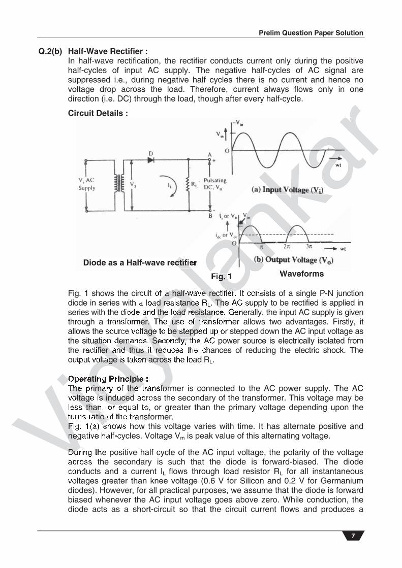
Q.2(b) Half-Wave Rectifier : In half-wave rectification, the rectifier conducts current only during the positive half-cycles of input AC supply. The negative half-cycles of AC signal are suppressed i.e., during negative half cycles there is no current and hence no voltage drop across the load. Therefore, current always flows only in one direction (i.e. DC) through the load, though after every half-cycle.
Circuit Details :
Fig. 1 shows the circuit of a half-wave rectifier. It consists of a single P-N junction diode in series with a load resistance RL. The AC supply to be rectified is applied in series with the diode and the load resistance. Generally, the input AC supply is given through a transformer. The use of transformer allows two advantages. Firstly, it allows the source voltage to be stepped up or stepped down the AC input voltage as the situation demands. Secondly, the AC power source is electrically isolated from the rectifier and thus it reduces the chances of reducing the electric shock. The output voltage is taken across the load RL.
Operating Principle : The primary of the transformer is connected to the AC power supply. The AC voltage is induced across the secondary of the transformer. This voltage may be less than, or equal to, or greater than the primary voltage depending upon the turns ratio of the transformer. Fig. 1(a) shows how this voltage varies with time. It has alternate positive and negative half-cycles. Voltage Vm is peak value of this alternating voltage.
During the positive half cycle of the AC input voltage, the polarity of the voltage across the secondary is such that the diode is forward-biased. The diode conducts and a current IL flows through load resistor RL for all instantaneous voltages greater than knee voltage (0.6 V for Silicon and 0.2 V for Germanium diodes). However, for all practical purposes, we assume that the diode is forward biased whenever the AC input voltage goes above zero. While conduction, the diode acts as a short-circuit so that the circuit current flows and produces a
Diode as a Half-wave rectifier Waveforms Fig. 1
Vidy
alalaalaala a half-wave rectifier. ald resistance . The
yal and the load resistan
yamer. The use of tran
yatage to be steppe
dyauation demands. Secondly, th
dya
ifier and thus it red
dy voltage is taken across
idyidyOperating Principle
VidyThe primary of the transfor
Vidoltage is induced
Vids than, or eq
Vid atio o
ViFig. 1(a) sVneVVDuVV
arrrrarararaaaank
alaectifi
Fig. 1g. g. g. 1

Vidyalankar : S.Y. Diploma BEM
8
voltage across the load resistor RL. This current makes the terminal A positive with respect to terminal B. Therefore, the voltage appearing across the load terminals A and B is practically the same as that of the positive input half cycle of AC input voltage as shown in Fig. 1(b).
During the negative half-cycle of the input voltage, the polarity gets reversed so that the diode is reverse biased. Hence, it does not conduct and practically there is no flow of current through the circuit. Therefore, almost no voltage is developed across the load resistor RL i.e. V0= 0. All the input voltage now appears across the diode itself. The result is that only the positive half cycle of the AC input voltage is utilized for delivering DC power and the output voltage is almost the same as the input voltage. The complete waveform of the output voltage across the load RL is as shown in Fig. 1(b).
It is evident that though the output voltage is not a steady (or perfect) DC is at least unidirectional. But it is only a pulsating DC wave having the frequency equal to the input voltage frequency. It is evident from the above discussion that as the circuit uses only one-half cycle of the AC input voltage, therefore it is popularly known as a half-wave rectifier.
Q.2(c) Important Terms : (i) Peak Inverse Voltage (PIV):
The maximum value of reverse voltage that a diode can withstand without destroying its P-N junction during the non-conduction period is called peak inverse voltage. The diode should be so chosen as to withstand this reverse voltage.
(ii) Ripple factor:
The ripple factor of a rectifier is a ratio of r.m.s. value of the alternating components in the load to the DC components in the load of a rectifier. It is denoted by a letter V which is defined as :
RMS value of AC components in the load
rAverage or d.c. components in the load
2
rms
dc
I1
I
It is an indication of how successful is a rectifier circuit in converting AC to DC. The ripple factor of half-wave and full-wave rectifier is 1.21 and 0.482 respectively. Thus, ripple factor is a measure of purity of the DC output of a rectifier.
(iii) Rectification efficiency :
The rectification efficiency of a rectifier is a ratio of the DC power output delivered to the load to the AC power input supplied to the rectifier circuit. It is denoted by a latter t|, which is defined as
DC power output
AC input power from transformer secondary
It is a figure of merit (a measure of efficiency) to compare different rectifiers. The maximum rectification efficiency of half-wave and full wave rectifier is 40.6% and 81.2% respectively.
rhererage is
are now
ar alf cycle of
artput voltage is
karm of the outp
kakakaady (or perfect) DC is at leka the frequency equal t
nka
ussion that as th
nk herefore it is pop
nkank
ananlan everse voltage that a diode
laon during the non-condula should be so chosen
alaalaalaalf a rectifier is a r
ya the load to the DC c
yater V which is de
dya
dyRMS value of
rAverage or d.c
dy
idy is an indication of how
VidyC. The ripple factor of
Vidyrespectively. T
Vidrectifier.
Vid
Vi(iii) RectificViVVV

Prelim Question Paper Solution
9
(iv) Transformer Utilization Factor (TUF): It is the ratio of DC power delivered to the load to the AC rating of the transformer secondary. It is denoted as TUF and is defined as :
DC power de livered to the load
TUFAC rating of the transformer secondary
The TUF for a halfwave rectifier is 0.287 whereas for centre-tap and bridge rectifier is 0.693 and 0.812 respectively.
Q.2(d) Capacitor Input (Or ) Filter :
Principle of Operation : When the additional DC voltage across L1 cannot be tolerated in the circuit of a Fig. 1, a CLC filter will give a similar magnitude of ripple, but with poorer voltage regulation. Fig. 1 shows a network for a capacitor input filter circuit. It consists of a filter capacitor C1 connected across the rectifier output, a choke L in series and another filter capacitor C2 connected across the load resistor RL. Only one filter section is shown, but several such identical sections are often used to improve the smoothing action. This filter is called a filter as its shape is like a Greek letter (pi). The rectifier feeds output directly into the capacitor C1. Therefore, this filter is also called capacitor input filter.
The pulsating output from the rectifier is applied at the input terminals of the capacitor-input filter. The action of this filter can be understood by looking this filter made up of two parts : (i) Shunt capacitor filter formed by capacitor C1. (ii) LC filter formed by choke L and capacitor C2.
Here the rectifier output first charges the capacitor GI to the peak value of the rectifier output This capacitor tends to hold this charge between successive peaks discharging slowly through the choke L and the load resistor RL. As a result, the filter output voltage drops slightly between the successive peaks as shown in Fig. 1. The capacitor input filter thus gives a higher output voltage than that of a choke-input filter for the same AC input voltage. The remaining output fluctuations are opposed by the series choke and bypassed to ground through the capacitor C2. The output voltage of this filter falls rapidly with increasing load current. This means that the voltage regulation of a capacitor input filter is not as good as that of a choke-input filter.
Fig. 1 : Capacitor input filter Fig. 2 : Rectifier and filteroutput waveform
Vidydydydy pulsating output from t
idycapacitor-input filter. The ac
Vidyilter made up of two parts :
Vidy(i) Shunt capacito
Vid LC filter form
Vid
ViHere the reVreVpeaVresuVa
karrdgerarkar
kar the circuit of a
ka with poorer voltage
kakankacuit. It consists o
nkput, a choke L in se
nk load resistor RL.nk sections are often us
an filter as its shap
andirectly into the
an filter.
lan
Vdy
aFig. 1 : Capacitor input f

Vidyalankar : S.Y. Diploma BEM
10
Since the rectifier feeds into the capacitor C1, the capacitor input filter can be used together with a half-wave rectifier whereas the choke-input filter cannot be used with a half-wave filter. The ripple factor (for 50 Hz mains supply) of a -filter is given by the relation,
2
1 2 L1 2 L
1 5700r
C C LR4 2 C C L R
where, C1 and C2 are in microfarad ( F), L is in henry (H) and RL in ohm ( ). It is evident from the above relation that the ripple factor in a -filter is dependent only on the product of the capacitance values of the capacitors C1 and C2. But the DC output voltage will be high only if the value of capacitor C1 is large. Hence, for a given ripple factor, the -filter is designed with a large value of capacitor C1.
It should be noted that under some conditions of small load currents, it is possible to replace the choke L1, with a resistor R equal in value to the reactance of choke L1 at the ripple frequency of 100 Hz without changing the ripple factor. However, the increased resistance of DC current flow will make this impractical except where the load current is very small. The approximate value of the resistor R may be 100 to 200 . It is then called capacitor input RC filter. This means a saving in the expense, weight and space of the choke. Such a replacement of a resistor R for a choke L1, is often practical only for low-current power-supplies.
Advantages : Main advantages of a -filter are : (i) Smaller ripple factor than that obtained by the use of multisection LC filter
with the same total value of L and C. (ii) Higher DC output voltage (Vdc = Vm) at high loads.
Disadvantages : The disadvantages of a -filter are : (i) It has poorer voltage regulation, as it has increased voltage drop in the filter. (ii) It has increased peak anode current. (iii) It requires higher PIV. (iv) It is costlier and bulky.
Q.2(e) NPN transistor working and diagram npn Transistor : Forward-Active Mode Opertaion If the transistor is used as an amplifying device, the base-emitter (B E)
junction is forward biased and the base-collector (B-C) junction is reverse biased, in a configuration called forward-active operating mode or simply the active mode.
Vidy
alank
arrrar)
arkarer is depend
karrs C1 and C2. But
kae of capacitor C1 is large.
kasigned with a large value kanka
nks of small load
nk R equal in value to
ank without changing t
an current flow will ma
anry small. The a
lan0 s then called capac
lapense, weight and spacla a choke L1, often
alaalaalaalfilter are :
ya actor than that obta
yaotal value of L an
dyagher DC output voltage (Vdc =
dya
dyantages
dy isadvantages -filt
idy(i) It has poorer voltage regu
Vidy(ii) It has increased peak an
Vidyiii) It requires high
Vid It is costlier
Vid
ViQ.2(e) NPN transVV VVV

Prelim Question Paper Solution
11
An npn bipolar transistor biased in the forward-active mode. Emitter of the transistor is n-type mean majority carrier in the emitter region
are electrons since the B-E junction is forward biased, electrons from the emitter are injected across the B-E junction into the base as shown by an arrow.
Since the B-C junction is reverse biased the electron centralization at the edge of that junction (B-C junction) is approximately zero.
So electrons from n-type emitter are injected into Base region and at the same there are less no. of electonsin B-C junction this creates large concentration gradient in the base region.
Because of above mentioned concentration gradient, electrons injected from the emitter diffuse across the base into the B-C space charge region, where the electric field sweeps them into the collector region.
Q.3(a) iC = iB = 150 (15 A) = 2.25mA
iE = ( 1 + ) iB = (151) (15 A) = 2.27mA
= 1
= 150151
= 0.9934
Q.3(b) Common-Emitter (CE) Configuration
C n P n
RC RE
E Electron
Base-collector (B-C) junction
Base-emitter (B-E) junction
iE iC
+ VBE B
VBB + + VCC
RC
VCC
VBB
RB B
VBE +
E
VCE
iC
iB
C
n
P
n
iE
Vidy
alank
arrrararkar
kar
kakaka mod ka arrier in the emitter re
nka
sed, electrons f
nk into the base a
nkankd the electron ce
an approximately zero.
an are injected into
lano. of electonsin B-C junc
la the base region.
alaed concentration g
alass the base into the B
alaeps them into the calya= 150 (15 A)
ya = (151) A
dya
d1
= ya01
dydymon-Emitter (CE) Con
idyVidy
Vidy
Vid
Vid
ViVVVVV

Vidyalankar : S.Y. Diploma BEM
12
An npn transistor circuit in the common-emitter configuration. When emitter terminal is made common as both the input as well as the
output BJT is said to operates in common emitter configuration.
Input Characteristics
Input characteristics are curves of variation of input current (iB) against input voltage (VBE) at constant output voltage (VCE).
When VCE increases, junction width increases, base width decreases, due to the decrease in recombination in base the base current iB decreases.
The dynamic input impedance.
i = CE
BE
B V constant
V
I
Output Characteristics These are curves of variation of output current (IC) against output voltage (VCE) at constant input current (IB).
VCE E
C
iC RC
VCC
VBB VBE
B
iB +
0.7V VB (Volts)
IB1 > IB2 > IB1
IB3 IB2
IB1
A
VC
E =
4V
VC
E =
2V
VC
E =
0V
IB
(iB)
Vidy
alank
arrrrararkar
kar
kakagurat kah the input as well as
nkanfiguration.
nknkank
ananlanlalaalaalaalyal
yayadya
dya
dydyidynput characteristics are
Vidyoltage ) at constant
Vid When VCE incr
Vidthe decreas
Vid
e dynVi VVVdydy
ady
aIB1
IB
CE =
4 =
VVV
=
2V
=
V
aaaaaE
CV
=
alayala
yala

Prelim Question Paper Solution
13
From the transistor output characteristics it can be seen that IC is independent of VCE but depends on IB. Hence transistor operates as a current controlled current source (CCCS).
The dynamic output impedance is given by
0 = B
CE
C I constant
V
I
[Explanation for saturation region, Active region, and cut-off region are same as in CB configuration]
Q.3(c) Need of Cascade Amplifier :
An amplifier is the basic building block of most of the electronic systems. Just as one brick does not make a house, a single stage amplifier is not sufficient to construct a practical electronic system. The gain of a single stage small signal amplifier is limited and it is not sufficient for all practical applications. Therefore, in order to achieve more voltage gain and power gain, we have to use more than one stage of amplification, such an amplifier is called a multistage amplifier. To achieve this, the output of each amplifier stage is coupled in some way to the input of the next stage. Such a connection of amplifiers is called cascading. The resulting amplifier is also called cascaded amplifier. Much higher gain can be obtained from the multistage amplifiers. The amplifier used in radio and television receivers is, usually, a multistage amplifier.
A transistor circuit containing more than one stage of amplification is known as multistage transistor amplifier. A multistage amplifier using two or more single stage C.E. amplifiers is called a cascade amplifier. On the other hand, a multistage amplifier with CE amplifier as the first stage and CB (or CC) amplifier as the second stage is called a cascade amplifier.
Coupling Used In Amplifiers : In a multistage amplifier, the output of one stage becomes the input of the next stage. The output terminals of one amplifier cannot be connected directly to the input terminals of the next amplifier all the times due to some practical difficulties.
Saturation region 110 (V)
IC (mA)
Active Region
IB = 0
IB = 20 A
IB = 40 A
IB = 60 A
IB = 80 A
VCE (Volts)
1
2
3
4
5
Ic = ICE = 0
Cut-off region “OFF”
Output characteristics of npn transistor in CE configuration
Vidy
alank
arrrararkar
kar
kakakanka
nknks it can be senknce transistor operat
anan iven by
lanalaegion, Active regio
alaalaallifier :
ya basic building block o
ya make a house,
dyact a practical electronic sys
dyaer is limited and it i
dy o achieve more vo
dyage of amplification, s
idyve this, the output of e
Vidyinput of the next stage. Such
Vidyresulting amplifier
Vidtained from the
Vidvers is
ViVA VmuVstagVV
kaIB = 0 0 0 0
(Volts)
E configuration configuration

Vidyalankar : S.Y. Diploma BEM
14
As a matter of fact, all amplifier need some kind of coupling networks. Even a single stage amplifiers needs coupling to the input source and output load. The multistage amplifiers need a suitable coupling between two stages so that a minimum loss of voltage occurs when the signal passes through this coupling network to the next stage. Also, the DC voltage at the output of one stage should not be permitted to go to the input of the next
Q.3(d) Two Stage Direct Coupled (DC) CE Amplifier : The transformer coupled amplifiers suffer from the drawback that they cannot amplify the very low frequency signals (i.e. below 10 Hz) including direct current of zero frequency. This limitation is overcome by the use of Direct Coupled (DC) amplifier. It is also called as DC amplifier. It may be noted that the capacitors, inductors and transformers cannot be used as a coupling network at very low frequencies because the size of these passive components becomes very large at very low frequencies. In this method, amplifiers are connected directly without any intervening coupling devices. This type of coupling is known as direct coupling.
Circuit Details : It may be noted that the output of first stage is directly connected to the base of the next transistor Q2. Moreover, there are no input or output coupling capacitors and also the emitter bypass capacitors. Since there are no coupling capacitors between the two stages, there is a DC as well as AC interaction between the stages. The input resistance of the second stage is very large and loading of the first stage is very low.
Applications : The applications of direct coupled amplifier are as follows : (i) It is used is analog computation. (ii) It is used in power supply voltage regulators. (iii) It is used for bioelectric measurements. (iv) It is used in linear integrated circuits.
Two stage direct coupled CE amplifier
Vidy
ViVApVTheV(i) VVala
nkarrrar canno
ar direct current
kar Coupled (DC)
kar the capacitors,
ka network at very low
kaponents becomes very larkae connected directly with
nkapling is known a
nknknkan s directly connec
an are no input or
anrs. Since there are
lanere is a DC as well as AC la of the second stage is ve
alad

Prelim Question Paper Solution
15
Q.3(e) Comparison Of Different Types of Couplings : The performance of different types of coupling is as given below :
Sr. No. Particulars RC coupling Transformer
coupling Direct coupling
(i) Cost Less More Least (ii) Space and Weight Less More Least (iii) Frequency response Excellent in A.F. Poor Best (iv) Impedance matching Not good Excellent Good (v) Distortion Amplitude Frequency No distortion (vi) Hum No More Less (vii) Voltage gain Least More less (viii) Application Voltage
amplification Power amplification
Amplifying extremely low frequencies
Q.4(a) Parameters of op-amp
(i) Input bias current (IB) : Input bias current is the average of the currents flowing into the two input terminals of the op-amp.
1BI , is current flowing into
non-inverting and 2BI is current flowing into inverting terminal.
Input bias current IB = 1 2B BI I
2
1BI and 2BI must be zero but practically
1BI and 2BI is having a finite value due
finite value of input resistance Ri.
(ii) Input offset current (Iios) : The difference between the currents flowing into the inverting and non-inverting terminals of op-amp is called as input offset current Iios.
Iios = 1 2B B| I I |
(a) Ideally it is zero, practically it is in nanoamp. (b) This offset current exist due to mismatch of internal transistor.
(iii) Open loop voltage gain (Av) : It is gain of amplifier in open loop mode. Open loop mode is the mode of operation without any feedback. V0 = A Vd A Open loop gain 2 105
(iv) Differential input resistance (Ri) : is defined as resistance which can be measured at either the inverting or non-inverting terminal with the other terminal connected to ground.
It is few mega for transistor input stage and extremely high (thousand of G ) for op-amp having FET based input stages. Ri = 2M .
Vidy
alank
arrrrrrarararararstortio
arkkkar
karss
kar
kkkar
kars
kar
kkkcatio kakamplifying
kamely kalow frequenciekkkaaanka
nk current is the average of the curt is the average os of the op-amp. op-a
1BI , is current flow, is curr
flowing into inverting terminal. g into inverting termin
= = la1 2B B1
I IB
22
be zero but practically but practically 11BBII and an
2BI is
input resistance R esistance Ri.
fset current (Irrent (Iiosos) :) : The difference e diffverting and non-inverting terminalsd non-inverting t
rent Ire ios. IIiosios =
1 21B BB11|| I IIBB ||
(a) Ideally it is zero (a) Ideally it is , practical prac (b) This offset current exis (b) This offset current ex
(iii) Open loop voltage gii) Open loop vo Open loop mode is Open loop V V00 = A V A A O
(iv) Differen(iv) meascon

Vidyalankar : S.Y. Diploma BEM
16
Q.4(b) (i) Gain B. W. = 5MH3 as Gain = 1 B. W. = 5MH3
(ii) Saturation voltage = 1 v i.e. Vp = 14V
S.R. = 6
p
6 6
2 fV 2 5 10 14
10 10
S.R. = 439.8 V/ sec.
Q.4(c) Inverting Amplifier : In the inverting amplifier, input is applied to the inverting input of Op-amp and the non-inverting input terminal is grounded. VNI = V1 = 0 V VINV = V2 = Vin V0 = A (VNI VINV) = A (0 Vin) = A Vin
The negative sign indicates that the output voltage is out of phase w.r.t. input by 180 . Thus, in the inverting amplifier the input signal is amplified by gain A and the output is inverted. Non-Inverting Amplifier : In the open loop non-inverting configuration, the input is applied to the non-inverting input terminal and the inverting terminal is connected to ground. VNI = V1 = Vin VINV = V2 = 0 V0 = A (V1 V2) = A (VNI VINV) = A (Vin 0) = A Vin Thus, the output voltage is greater than the input voltage by gain A times and is in phase with the input signal.
Q.4(d) Summing, Scaling and Averaging Amplifier (Inverting Mode)
Rin
2
+ 3
Vin
+
741C
7
4
6
VEE
+VCC
V0
V1
V2
Rin
2
+ 3
Vin
+
741C
7
4
6
VEE
+VCC
V0
V1
V2
V1
V2
2
+ 3
741C
7
4
6
VEE
VCC
V0
ROM RL
V2
Rf
Rb
Ra
Rc
Rd Id
Ic
Ib
Iava
vb
vc
vd V1
Vid Ib Vidy
alank
arar output
by 180 . r the input input
and the output output
er : In the open loop e open loop ration, the input is applied the input is applied
ng input terminal and the ut terminal and thal is connected to ground. ected to ground.
= Vin V2 = 0
= A (V = 11 V2) = A (V = A (VNINI V VINV) = A (V= A (Vinin 0) = A V 0) = in
hus, the output voltage is greater te output voltage is input voltage by gain A times and i voltage by gain A timeswith the input signal. with the input signal
Vidy
Vidy.4(d) Summing, Scaling
kaaakankkkakaaakakannnnnnnn
3
nknknkVin
+
7477
4
66
VVEE EE
+VCC
VV0 0
VV11
2
a 2aaa +
V2
I
Iava
vb
Prelim Question Paper Solution
17
Scaling Amplifier : As shown in the above circuit diagram, a number of voltage sources can be connected to the inverting input of op-amp. The value of voltages and resistors can be varied. For an ideal op-amp, AV =
AV = 0
id
V
V =
Vid = 0V = 0
Vid = V1 V2 = 0
V1 = V2
Since V1 = 0, V2 = 0 (By concept of "VIRTUAL GROUND") As Ri = , for ideal op-amp, IB 0. Applying KCL at the inverting input terminal, Ia + Ib + Ic + Id = If ( IB 0)
a 2 b 2 c 2 d 2 2 0
a b c d f
V V V V V V V V V V
R R R R R
V2 = 0 (By concept of VIRTUAL GROUND)
a b c d 0
a b c d f
V V V V V
R R R R R
f f f f0 a b c d
a b c d
R R R RV V V V V
R R R R
Thus, the circuit works as a scaling amplifier, since each voltage is multiplied by different scaling factors. Summing Amplifier : In the above circuit, if Ra = Rb = Rc = Rd = Rf = R then each scaling factor becomes unity.
V0 = (Va + Vb + Vc + Vd) Since the output voltage is a ve sum of all input voltages, this circuit is known as a Summation Amplifier in inverting mode. Average Amplifier : In the above circuit, if Ra = Rb = Rc = Rd = Rf = R
V0 = fa b c d
R(V V V V )
R
Let fR 1R n
where n is the no. of input signals
fR 1R 4
V0 = a b c d
1(V V V V )
4
Vidy
alank
ar of "VIRTUAL GROUND") VIRTUAL GROUND")
al,
an2 2 00
d ff
V V VV2 2 00
R RRd
(By concept of VIRTUAL GR (By concept of VIRTU
0
f
0
R
fb c dc d
b c dc
R R RR Rf ff VVf f ffdd
f ff
R R RR Rb ccb cc
cuit works as a scaling amprks as a scaling amplifier, sicaling factors. tors
ming Amplifier :ing Amplifie the above circuit, if Rove circuit, if Raa = Rb = R
then each scaling factor becomes u ach scaling factor bec V00 = = (Va + V + Vbb + V c + V Vdd) )
Since the output voltage is a Since the output voltage is a a Summation Amplifier in ina Summation Amplifier in in
Average Amplifier :age AIn the above circuitIn the abov
V 0 = fR(
R
Let VfR
R

Vidyalankar : S.Y. Diploma BEM
18
Summing, Averaging Amplifier (Non-inverting Mode) : The op-amp is used in the non-inverting mode and 3 D.C. voltages Va, Vb and Vc are given to the +ve input terminal through resistors of same value. For a non-inverting amplifier,
Afb = 1 + f
1
R
R
To find the expression for the output voltage, apply superposition theorem. (i) Va is kept in the circuit with Vb and Vc replaced by the equivalent short circuit. Applying potential divider formula,
1 a
R / 2V V
R (R / 2) = a
R / 2V
3R / 2
a1
VV
3 … (i)
Similarly for the other two voltage sources Vb and Vc.
b1
VV
3 … (ii)
c1
VV
3 …(iii)
By superposition theorem,
V1 = 1 1 1V V V = a b cV V V
3 3 3
V1 = a b cV V V
3
This is the input to the non-inverting amplifier whose gain is f
1
R1
R.
V0 = gain V1 = a b cf
1
V V VR1
R 3
Summation Amplifier :
Let f
1
R1
R = n = 3
f
1
R
R = 2
Rf = 2 R1
2
+ 3
741C
7
4
6
VEE
VCC
V0
V2
Rf
R
R
R
va
vb
vc
V1
R1
R/2
R
R
R
Va
V1 NI i/p NI i/p
R V1
y the equivalent short circuit. y the equivalent short circuit.
er two voltage sources oltage source
… (ii) … (ii)
ycVc
3 …(iii) …(iii)
y superposition theorem, superposition theorem,
V1 = 1 1 11 1 1V V VV V V1 1 11 1 1 = = ya bV V Va b
3 33
V 11 = =
This is the input to thThis is the inp
V0 = ga
SummatiS
Let
rrraaa4
6
VEE EE
VV0 0
knknkR/
aaaaaaaaaaaaaaankk
aaaaaaaaaaaaR
R
alalaanV1 NINI i/pi/p kkknkkkknkknkkknkkknknkknkkk
NI i/pRR VV1 1

Prelim Question Paper Solution
19
Thus, suitable value of Rf and R1 can be selected.
V0 = a b cf
1
V V VR1
R 3 = a b cV V V
33
V0 = Va + Vb + Vc Average Amplifier :
Let f
1
R1
R = 1
This is done by making Rf = 0 and R1 = , i.e., the op-amp is used as a "Voltage follower".
V0 = a b cf
1
V V VR1
R 3
V0 = a b cV V V
3
Note : In case of non-inverting configuration as summing and average amplifier, all the resistors must be same through the various input voltages. This is not the case in inverting configuration (Ra, Rb, Rc). Hence, non-inverting mode cannot be used as "SCALING AMPLIFIER".
Q.4(e) INSTRUMENTATION AMPLIFIER
(i) In many industrial application, physical quantities like temperature pressure, humidity, light intensity are required to be measured and controlled. Transducers which convert energy from one form to another form are used for this purpose. e.g. Thermocouple, LDR strain gauge etc. In analogy instrumentation, these transducers are frequently located some distance away from measurement system. The signal levels at the transducer side are often low and their source impedance are high. A special purpose amplifier is required to amplify these signals. These are known as instrumentation amplifier.
(ii) Instrumentation system is used to measured the output signals produced by
a transducer and often to control the physical signals producing it. Many transducer produce output which do not have sufficient strength To amplify the low-level output produced by transducer is the main function
of instrumentation amplifier so that it can driven display or indicator (iii) Instrumentation system consist of 3 blocks Input stage is transducers and
pre-amplifier which is used to convert physical quantity in to electrical signal.
I/P Stage
Intermediate Stage
O/P Stage Physical
quantity to be measured
Transducers + pre-
amplifier
Instrumentation amplifier
Indicator and automatic process controllers
oscilloscope magnetic reach display
s used as a "Voltage as a "Voltage
ion as summing and average ampl summing and ave the various input voltages. ous input voltages.
guration (R Raa, R, Rbb, Rc). t be used as "SCALING AMPLIFIERed as "SCALING AM
anlanIFIE
(i) In many industrial application many industrial applichumidity, light intensity aumidity, light intensity Transducers which converansducers which convethis purpose. e.g. Tthis purpose. instrumentation, theinstrumentatfrom measuremeom mlow and their anrequired to a
(ii) Instrum (ii)
a tra M
tageIntermediate Intermedia
Stage Stage O
alalalaaTransducersnsducer+ pre- pre
amplifier plifie
Instrumentationstrumamplifier aala

Vidyalankar : S.Y. Diploma BEM
20
This signal is amplified by pre-amplifier 2nd stage is instrumentation amplifier. As output of first is very low level signal which can not drive output stage so it is amplified by instrumentation amplifier and then given to output stage which may be indicator, records etc.
Requirement of Instrumentation Amplifier 1) Precise low level signal Amplification : Instrumentation Amplifier is
expected to amplify signals of very small amplitudes, gain should be high, accurate and stable.
2) Low noise : Instrumentation amplifier is a differential amplifier so it rejects noise so low noise.
3) Low thermal drift : Parameter of instrumentation amplifier should not change due to temperature variations.
4) High input resistance : Instrumentation Amplifier must have a very high input impedance to avoid loading of input source.
5) Accurate closed loop gain and easy gain adjustment : Closed loop gain should be accurate as well as adjustable using potentiometer
6) Low power dissipation : Power consumption should be as low as possible. 7) High CMRR : High CMRR in order to reject common mode noise at the input
of instrumentation amplifier. 8) High slew rate : Transducer output are fast varying signals (high frequency
signals). So slew rate of op-amplifier should be high to ensure maximum undistorted output voltage swing.
Q.5(a) BLOCK OF DIAGRAM OF IC 555 AND ITS OPERATION
Timer IC 555 Functional diagram
R
S
F/ F
Q2
Vref
Q1
Discharge
Trigger 5k
C2
C1
5k Control Voltage
Threshold 5k
+ VCC
(Internal)
Q
GND
Buffer & Inverter
IC 555
8
4
5
2
7
3
1
6
Vidy
alank
arAmplifier is r is
ould be high, e high
mplifier so it rejects so it rejects
on amplifier should not ier should not
plifier must have a very high ifier must have a very hurce.
in adjustment : ment : Closed Closed loop gain loe using potentiometer g potentiomete
sumption should be as low as possn should be as lowr to reject common mode noise at thct common mode no
r output are fast varying signals (hiut are fast varyin op-amplifier should be high to en op-amplifier should be hi
ge swing. e sw laala5 AND ITS OPER
am
yydydydyddidyVid
Viddydydydddd
ViViViVVVyyy
Dis
Trigger
yy5k5ControlControl
VoltageVoltage
Threshold hold 5k5
+ VCC
dya
dydydyddydddyddddyddydydydydydydydydydyydyyyyVid
Vid
ViViVVdd

Prelim Question Paper Solution
21
Inverter symbol
OutputInput
The important internal block of the I.C. are (i) 2 No. of comparators : (a) Thresh hold comparator C1,
(b) Trigger comparator C2. (ii) R S F/F (iii) Buffer cum inverter (iv) 2 Transistors : (a) Discharge transistor Q1, (b) Reset Transistor Q2. (v) Potential divider formed by 3 equal value 5k resistors.
Operation : When the supply is given, the output depends upon the voltages at pin
no.2 (trigger) and 6 (thresh hold). If V2 > 1/3 VCC and V6 < CC2V
3are satisfied at the
start, the output of C1 and C2 are low, the F/F is reset. The output v0 = 0 and the circuit is in quiscent state. The internal Transistor Q1 is in saturation which clamps the pin 7 (discharge) to the ground potential. This prevents CEXT. from charging towards +VCC. Normally the quiscent condition is achieved by connecting pin 2 to +VCC through a resistor. Pin No.6 is connected to ground, through CEXT. (or R) .
Now to initiate, a negative going trigger pulse is given to pin 2 and its voltage is brought below vCC/3. The output of C2 goes high, thus S = 1 and R = 0. This sets the F/F. Q of F/F goes low, internal transistor Q1 is cut off and allows CEXT to charge. At the same time v0 = +VCC due to inverter. Normally pin No.6 is also tied to CEXT. When the CEXT. charges to (2/3) VCC, C1 comparator output goes high, making S = 0 and R = 1. The F/F is reset and its output Q =1. The final output at pin No.3 once again becomes 0 volt. The internal Transistor Q1 goes into saturation and CEXT. starts discharging through internal Q1 and some REXT connected at pin no.7.
Thus basically pin no.2 controls the trigger comparator and voltage at pin No.6 controls the thresh hold comparator C1. The output of these 2 comparators are used to control i..e set or reset the F/F. If F/F is reset then final v0 = 0 and internal Q1 is in saturation. On the other hand if F/F is set then v0 = +VCC and internal Q1 is cut off.
By connecting different components in different manners at pin nos. 2, 6, and 7, the I. C. can be used as Astable, Monostable, Bistable multivibrator, Schmitt trigger. Similarly varying the voltage at pin no.5 (control voltage), the circuit can be used as a voltage to frequency converter. By giving a negative pulse at pin No.4(Reset) and bringing it down to below +0.4v (Normally this pin is held at +VCC), any ongoing operation can be curtailed at any instant.
Q.5(b) (i) NOT gate : Consider a binary variable A. The NOT operation transforms A into the output NOT(A) with the following effect :
If A = 0, then NOT (A) = 1; If A = 1, then NOT (A) = 0.
Vidy
alank
are voltages at pin s at pin
C
3are satisfied at the satisfied at the
The output v v00 = 0 and the 0 and the s in saturation which clamps s in saturation which clamps
s prevents C prevents CEXT. from charging om chargs achieved by connecting pin 2 to eved by connecting pin
o ground, through C hrough CEXTEXT. (or R) . . (or
pulse is given to pin 2 and its voltag given to pin 2 an2 goes high, thus S = 1 and R = 0 high, thus S = 1 and
ternal transistor Qistor Q1 is cut ut off and ao +VCC due to inverter. Normally pindue to inverter.
charges to (2/3) V charges to (2/3) VCC, C C11 compara c = 1. The F/F is reset and its outpu 1. The F/F is reset and
again becomes 0 volt. The intern becomes 0 volt. TheEXT. starts discharging through inteischarging throu
o.7.
pin no.2 controls the trigger comp controls the trigge thresh hold comparator Chold comparator C11. The o
ontrol i..e set or reset the F/F. If set or reset the Q Q1 is in saturation. On the other n saturation. On the
nal Ql Q11 is cut is cut off. off.
By connecting different componentnnecting different comthe I. C. can be used as Astab C. can be used as Atrigger. Similarly varying the vtrigger. Similarly varying the be used as a voltage to frebe used as a voltage to freNo.4(Reset) and bringino.4(Reset) and +VCC), any ongoing op), any
ViViQ.5(b) (i)Consider output N
If A = If A

Vidyalankar : S.Y. Diploma BEM
22
(ii) OR Gate : Y = A + B (iii) AND Gate :
Y = A B (iv) NOR Gate : Y = A B
Q.5(c) B + CD = (A + C) (A + D) (B + C) (B + D)
RHS = (A + C) (A + D) (B + C) (B + D) = (AA + AD + AC + CD) (BB + BD + BC + CD) = (A + AD + AC + CD) (B + BD + BC + CD) … (A A = A) = [A (1 + D + C) + CD] [B (1 + B + C) + CD] = (A + CD) (B + CD) … ( 1 + B + C = 1 AND 1 + D + C = 1) = AB + ACD + BCD + CD … ( CD CD = CD) = AB + CD (A + B + 1) … ( A + B + 1 = 1) = AB + CD … ( A + B + 1 = 1) RHS = LHS … Hence proved.
Q.5(d)
(a) NOT OR cascade (b) NOR gate symbol
Vidy
alank
ar
alaala D) (B + C) (B + D)
+ C) (A + D) (B + C) (B + D) + D) (B + C) (B + D (AA + AD + AC + + AC + CD) (BB + BD + BCD) (BB +
= (A + AD + AC + CD) (B + BD + B AD + AC + CD) (B + = [A (1 + D + C) + CD] [B (1 + B + D + C) + CD] [B = (A + CD) (B + CD) … = (A + CD) (B + CD)
= AB + ACD + BCD + CD = AB + ACD + = AB + CD (A + B + 1) = AB + CD (A + = AB + CD = AB + CD
RHS = LHS RHS = LHS
Vidy
Vid.5(d)
(b) NOR gate symbolb) NOR gate symb
Prelim Question Paper Solution
23
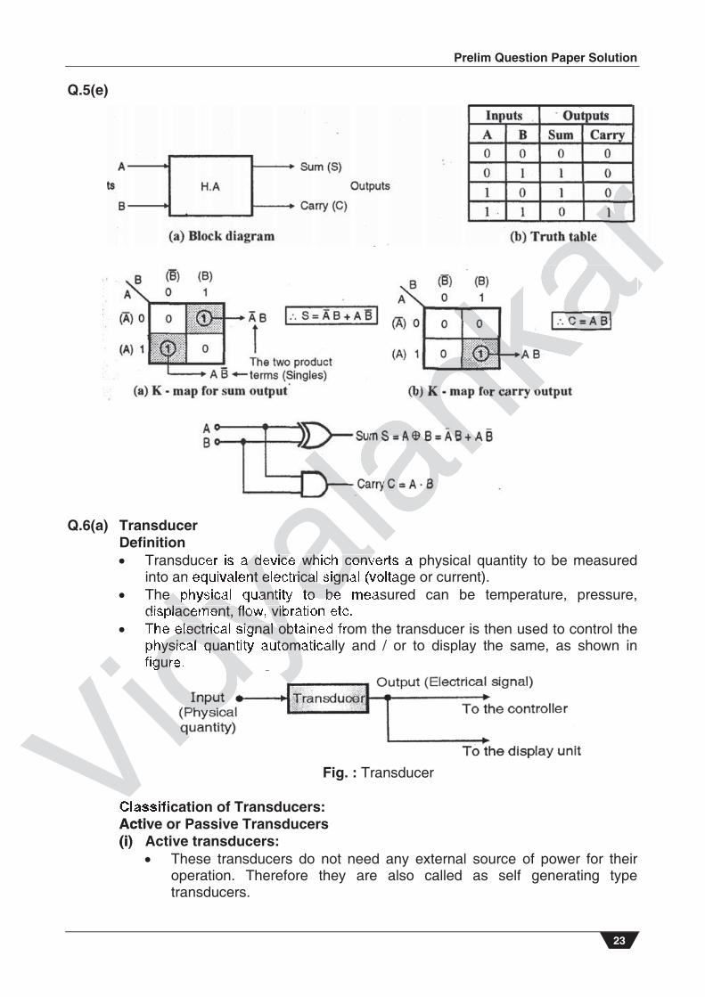
Q.5(e)
Q.6(a) Transducer
Definition Transducer is a device which converts a physical quantity to be measured
into an equivalent electrical signal (voltage or current). The physical quantity to be measured can be temperature, pressure,
displacement, flow, vibration etc. The electrical signal obtained from the transducer is then used to control the
physical quantity automatically and / or to display the same, as shown in figure.
Fig. : Transducer
Classification of Transducers: Active or Passive Transducers (i) Active transducers:
These transducers do not need any external source of power for their operation. Therefore they are also called as self generating type transducers.
Vidy
alank
ararkar
kar
anlanalaalaalya a device which conv
yant electrical signa
dyae physical quantity to be
dyaplacement, flow, vib
dy electrical signal obt
dyhysical quantity autom
idygur
Vid
VVVActive(i)
Vidyalankar : S.Y. Diploma BEM
24
The active transducers are self generating devices which operate under the energy conversion principle.
At the output of active transducers we get an equivalent electrical output signal e.g. temperature to electric potential, without any external source of energy being used.
Typical examples of active transducers are: Piezoelectric sensors: They generate a charge corresponding to
pressure. Photo voltaic cell: It produces an emf proportional to the intensity of
light incident on it. Thermocouple: It produces an emf proportional to the change in
temperature.
(ii) Passive transducers: These transducers need external power supply for their operation. So
they are not “self generating type” transducers. A DC power supply or an audio frequency generator is used as an
external power source. These transducers produce the output signal in the form of variation in
resistance, capacitance or some other electrical parameter in response to the quantity to be measured.
Typical examples of passive transducers are as follows: Strain gauge: Converts pressure into equivalent change in
resistance. Thermistor: Converts temperature variations into equivalent
resistance changes. Photodiode: Converts light intensity into current changes.
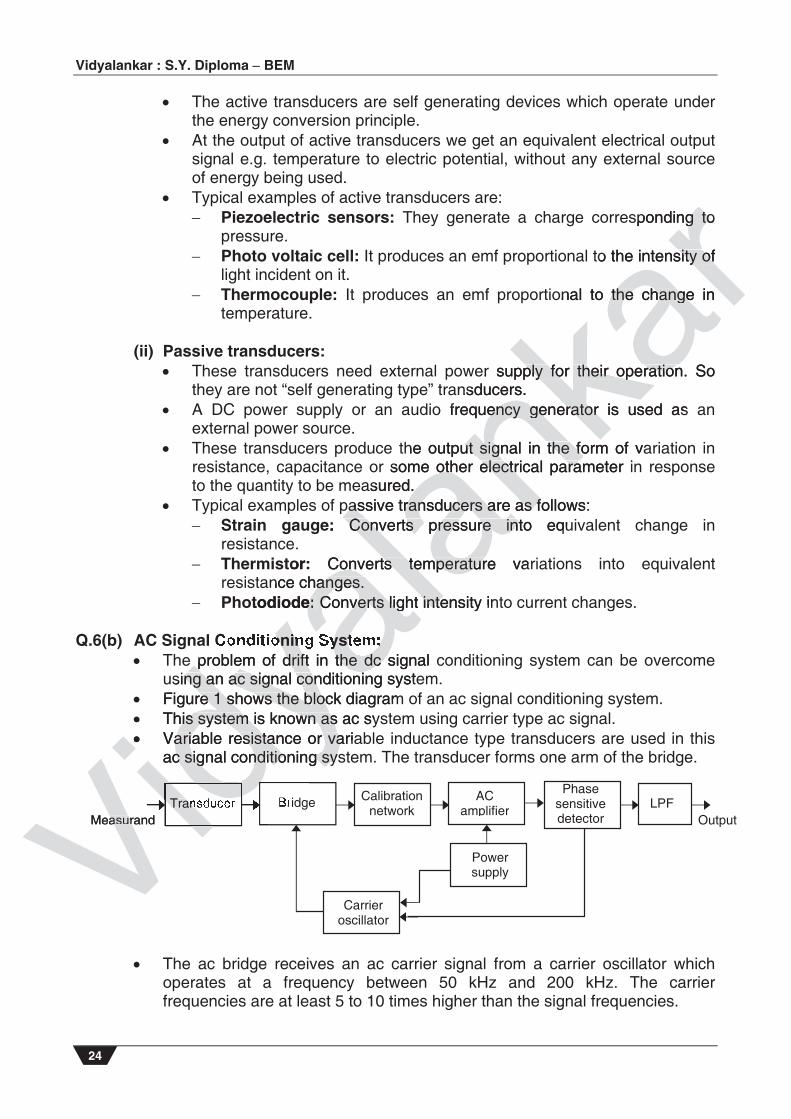
Q.6(b) AC Signal Conditioning System:
The problem of drift in the dc signal conditioning system can be overcome using an ac signal conditioning system.
Figure 1 shows the block diagram of an ac signal conditioning system. This system is known as ac system using carrier type ac signal. Variable resistance or variable inductance type transducers are used in this
ac signal conditioning system. The transducer forms one arm of the bridge. The ac bridge receives an ac carrier signal from a carrier oscillator which
operates at a frequency between 50 kHz and 200 kHz. The carrier frequencies are at least 5 to 10 times higher than the signal frequencies.
Transducer Bridge Calibration network
AC amplifier
LPF Phase
sensitive detector
Power supply
Measurand Output
Carrier oscillator Vi
dyala
nkar
sponding to g to
to the intensity of sity of
onal to the change in the change
er supply for their operation. So ply for their operationnsducers.
frequency generator is used as ency generator
the output siut signal in the form of vagnal in the fo some othe oth r electrical parameter i electrical para
asured. . passiv pas e transducers are as follows: ransducers are as f
e: Converts pressure into equ Converts pressure int
or: Converts temperature varConverts temperaturance changes. hanges.
todiode:e: Converts light intensity in Converts light inte
yayaoning System: problem of drift in the dc signal problem of drift in the dc c
sing an ac signal conditioning systeng an ac signal con Figure 1 shows the block diagramre 1 shows the bloc This system is known as ac syhis system is known as Variable resistance or variaariable resistance or va
ac signal conditioning sysc signal conditioning sys
Vid
VidTran ddd
VidMeasurand asur
Prelim Question Paper Solution
25
The output of transducer is applied to the bridge circuit. The output of this bridge is an amplitude modulated carrier signal.
An ac amplifier is used to amplify this amplitude modulated signal. An ac amplifier is RC coupled amplifier or transformer coupled amplifier.
The amplifier output is applied to a phase sensitive demodulator (detector). The phase sensitive detector produces a dc signal which indicates the direction of parameter change in the bridge output.
Advantages : (i) No frequency drift problem (ii) No spurious signal is present Disadvantage: (i) It is difficult to obtain a stable carrier oscillator frequency.
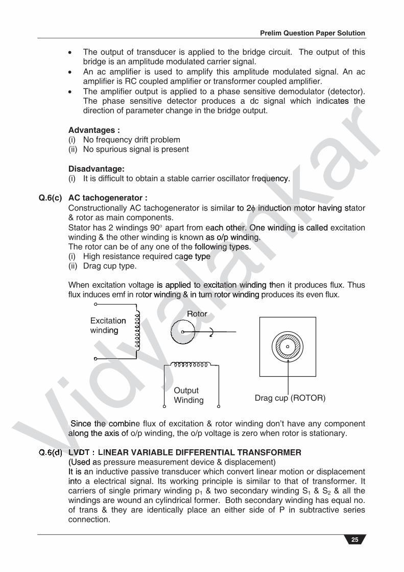
Q.6(c) AC tachogenerator : Constructionally AC tachogenerator is similar to 2 induction motor having stator & rotor as main components. Stator has 2 windings 90 apart from each other. One winding is called excitation winding & the other winding is known as o/p winding. The rotor can be of any one of the following types. (i) High resistance required cage type (ii) Drag cup type. When excitation voltage is applied to excitation winding then it produces flux. Thus flux induces emf in rotor winding & in turn rotor winding produces its even flux.
Since the combine flux of excitation & rotor winding don’t have any component along the axis of o/p winding, the o/p voltage is zero when rotor is stationary.
Q.6(d) LVDT : LINEAR VARIABLE DIFFERENTIAL TRANSFORMER (Used as pressure measurement device & displacement)
It is an inductive passive transducer which convert linear motion or displacement into a electrical signal. Its working principle is similar to that of transformer. It carriers of single primary winding p1 & two secondary winding S1 & S2 & all the windings are wound an cylindrical former. Both secondary winding has equal no. of trans & they are identically place an either side of P in subtractive series connection.
Drag cup (ROTOR)
Rotor Excitation winding
Output Winding
Vidy
alank
arec
ates th
requency. equen kanka
lar to 2 induction motor having sta induction mot
each other. One winding is called eer. One winding is cwn as o/p winding. p winding.
e following types. wing type cage type cage type
e is applied to excitation winding the to excitation win otor winding & in turn rotor winding prnding & in turn rotor win
Since the combine Since the along the axis of aloVVd) LVD
(Used asIt is aninto
yayayayayaaRotor Rotor
dydddyion
ding
dydydyyyyyyyydydydyyyyyyyyyyyyyyyy

Vidyalankar : S.Y. Diploma BEM
26
A movable soft iron care is placed inside the former one terminal of each secondary are brought outside.
Working : As mentioned before the working of LVDT is similar to a transformer. When we apply AC line voltage of 50Hz to 20KHz. Primary winding produced varing flux. This varing flux then links with secondary coil & induces an emf in it. Thus S1 emf induces in S1 & S2 emf in S2.
In order to get single o/p voltage 2 secondary winding S1 & S2 are connected in series opposition it means the induced voltage of each winding opposes each other. Thus 0 1 2e es es When the core is at null position then flux linking with both the secondary winding are equal & hence equal emf are induced in it.
0e 0 es1 = es2 Thus if core is more to left from null then more flux link with winding S1 & less flux with winding S2.
es1 > es2 magnitude of o/p voltage is in phase with
1se similarly when core is more to right
from null position then flux linking with S2 is more than that of winding S1 es2 > es1 & therefore o/p voltage is in phase with es2 i.e. o/p voltage of
secondary winding S2.
Secondary Winding S2
SOFT IRON CORE
Secondary Winding S1
Primary Winding P1
former
Arm Displacement Displacement
Displacement
Ac i/p
E0 = E1 E2
Primary winding
Ferromagnetic Core
Hollow Bobbin
E0
E1 E2
Zero Displacement
o/p of flux due to residual
= 180
E0
= 0
Linear range
Centre position of core
Vidy
alank
arring flu
. Thus SS11
ltage 2 secondary winding Stage 2 secondary winding 1 & Sns the induced voltage of each wie induced voltage of e
2es null position then osition then flux linking with bflux linking
e equal emf are induced in it. emf are induced in es1 = es2
e is more to left from null then moree to left from null theding S2.
s11 > es > e 2
agnitude of o/p voltage is in phase wde of o/p voltage is
from null position then flux linking w null position then flux lin ess22 > es 1 & therefore o/p & therefore o
secondary winding Secondary windin 2.
Secondary SecoWinding SWinding 2
kknknknknkkka
nPrimaryWinding Pding P11
former
Displacement acement
VVVVVVddddddddAc i/pAiPrimary mary
windingngVFerromagnetic FerromagnCoreCore

Prelim Question Paper Solution
27
Thus o/p voltage of LVDT linearly varies with displacement of core from null position. The figure shows the variation of o/p voltage with respect to displacement. As shown in figure as the core is more in one direction from null position then magnitude of o/p voltage goes on increasing but phase difference remains same i.e. 0. On the other hand when core is moved in other direction from null position then also magnitude of o/p goes on increasing but now phase difference is maintain at 180 . Thus by comparing magnitude & phase difference of secondary voltage with that of primary voltage then we can easily find out displacement of core. Advantages of LVDT : (i) Upto displacement of 5mm the o/p voltage of LVDT varies linearly. (ii) The o/p voltage of LVDT do not varies in step thus it gives better resolution. (iii) It gives high o/p voltage no need of amplification. (iv) It has high sensitivity upto 40 V/mm. (v) Since it do not have any sliding contact it use or gives less friction. (vi) It passes very less hysterisis losses.
Q.6(e) Rotameter : Rotameter is a variable area type of flow meter widely used for flow measurement.
It consists of vertical tapered tube with a float which is free to move in up and down direction. The free area between the float and inside wall of the tube is known as annular orifice. The tube is mounted vertically with a small end at the bottom. The fluid whose flow is to be measured enters the tube from bottom and passes upward around a float and leaves from the top. The venturi tubes are usually made of cast iron or select & are build in several shapes.
Outlet
Guide wire for float
floatTransparent tapered tube (Borosilicate glass)
X
Minimum annular area
Inlet
Maximum annular area
Vidy
alank
arw pha
tage with that ith thare.
ar aries linearly. arl it gives better resolution. s better resolution.
n. .
t use or gives less friction. ves less friction.
nknknkype of flow meter widely used w meter widel
It consist down dknowbo
nOutle
dyayadyaXX
Inlet
yaular
nyyayayyyaayayyayayaa
lanaalan
alaan
alalan
aady
alanan

Vidyalankar : S.Y. Diploma BEM
28
Advantages : (i) Causes low permanent pressure loss. (ii) Widely used for high flow rates. (iii) Available in very large pipe sizes. (iv) Has will known characteristics. (v) More accurate over wide flow ranges than orifice plates or nozzles. Disadvantages : (i) High Cost (ii) More difficult to inspect due to its construction. (iii) Limitation of a lower Reynolds number of 150,000.
Vidy
alank
ar