bas40 series; 1psxxsb4x series
TRANSCRIPT
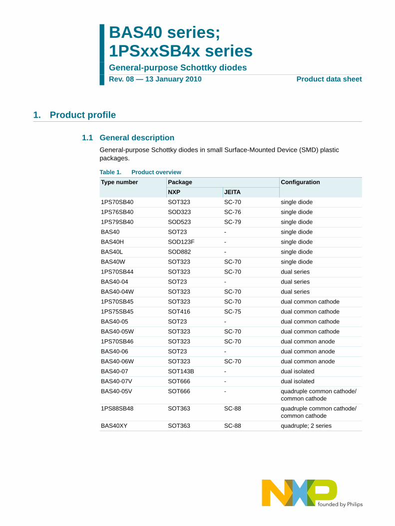
1. Product profile
1.1 General description
General-purpose Schottky diodes in small Surface-Mounted Device (SMD) plastic packages.
BAS40 series; 1PSxxSB4x seriesGeneral-purpose Schottky diodesRev. 08 — 13 January 2010 Product data sheet
Table 1. Product overview
Type number Package Configuration
NXP JEITA
1PS70SB40 SOT323 SC-70 single diode
1PS76SB40 SOD323 SC-76 single diode
1PS79SB40 SOD523 SC-79 single diode
BAS40 SOT23 - single diode
BAS40H SOD123F - single diode
BAS40L SOD882 - single diode
BAS40W SOT323 SC-70 single diode
1PS70SB44 SOT323 SC-70 dual series
BAS40-04 SOT23 - dual series
BAS40-04W SOT323 SC-70 dual series
1PS70SB45 SOT323 SC-70 dual common cathode
1PS75SB45 SOT416 SC-75 dual common cathode
BAS40-05 SOT23 - dual common cathode
BAS40-05W SOT323 SC-70 dual common cathode
1PS70SB46 SOT323 SC-70 dual common anode
BAS40-06 SOT23 - dual common anode
BAS40-06W SOT323 SC-70 dual common anode
BAS40-07 SOT143B - dual isolated
BAS40-07V SOT666 - dual isolated
BAS40-05V SOT666 - quadruple common cathode/ common cathode
1PS88SB48 SOT363 SC-88 quadruple common cathode/ common cathode
BAS40XY SOT363 SC-88 quadruple; 2 series
BAS40_1PSXXSB4X_SER_8 © NXP B.V. 2010. All rights reserved.
Product data sheet Rev. 08 — 13 January 2010 2 of 21
NXP Semiconductors BAS40 series; 1PSxxSB4x seriesGeneral-purpose Schottky diodes
1.2 Features
1.3 Applications
1.4 Quick reference data
[1] Pulse test: tp ≤ 300 μs; δ ≤ 0.02.
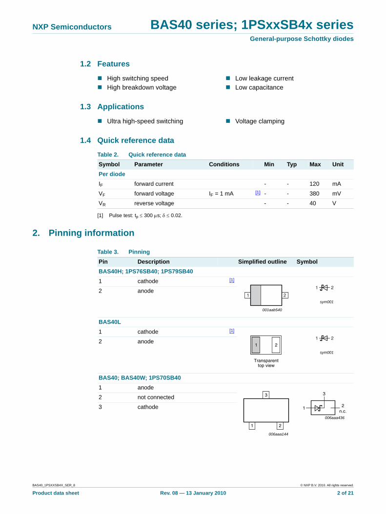
2. Pinning information
High switching speed Low leakage current
High breakdown voltage Low capacitance
Ultra high-speed switching Voltage clamping
Table 2. Quick reference data
Symbol Parameter Conditions Min Typ Max Unit
Per diode
IF forward current - - 120 mA
VF forward voltage IF = 1 mA [1] - - 380 mV
VR reverse voltage - - 40 V
Table 3. Pinning
Pin Description Simplified outline Symbol
BAS40H; 1PS76SB40; 1PS79SB40
1 cathode [1]
2 anode
BAS40L
1 cathode [1]
2 anode
BAS40; BAS40W; 1PS70SB40
1 anode
2 not connected
3 cathode
001aab540
1 2sym001
1 2
21
Transparenttop view
sym001
1 2
006aaa144
1 2
3
006aaa436
1
3
2n.c.
BAS40_1PSXXSB4X_SER_8 © NXP B.V. 2010. All rights reserved.
Product data sheet Rev. 08 — 13 January 2010 3 of 21
NXP Semiconductors BAS40 series; 1PSxxSB4x seriesGeneral-purpose Schottky diodes
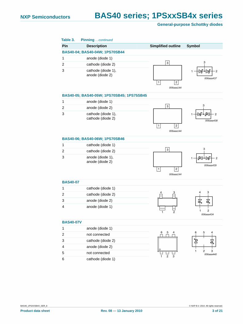
BAS40-04; BAS40-04W; 1PS70SB44
1 anode (diode 1)
2 cathode (diode 2)
3 cathode (diode 1), anode (diode 2)
BAS40-05; BAS40-05W; 1PS70SB45; 1PS75SB45
1 anode (diode 1)
2 anode (diode 2)
3 cathode (diode 1), cathode (diode 2)
BAS40-06; BAS40-06W; 1PS70SB46
1 cathode (diode 1)
2 cathode (diode 2)
3 anode (diode 1), anode (diode 2)
BAS40-07
1 cathode (diode 1)
2 cathode (diode 2)
3 anode (diode 2)
4 anode (diode 1)
BAS40-07V
1 anode (diode 1)
2 not connected
3 cathode (diode 2)
4 anode (diode 2)
5 not connected
6 cathode (diode 1)
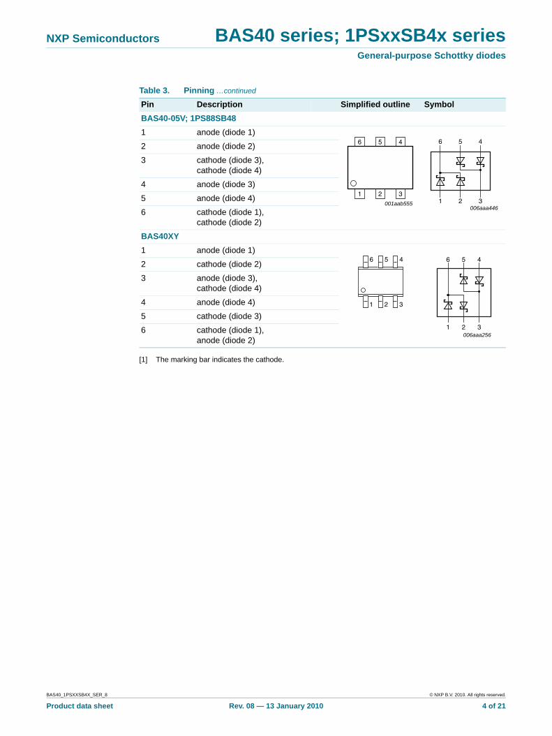
Table 3. Pinning …continued
Pin Description Simplified outline Symbol
006aaa144
1 2
3
006aaa437
1 2
3
006aaa144
1 2
3
006aaa438
1 2
3
006aaa144
1 2
3
006aaa439
1 2
3
21
34
006aaa434
2
34
1
1 2 3
456
006aaa440
6 5 4
1 2 3
BAS40_1PSXXSB4X_SER_8 © NXP B.V. 2010. All rights reserved.
Product data sheet Rev. 08 — 13 January 2010 4 of 21
NXP Semiconductors BAS40 series; 1PSxxSB4x seriesGeneral-purpose Schottky diodes
[1] The marking bar indicates the cathode.
BAS40-05V; 1PS88SB48
1 anode (diode 1)
2 anode (diode 2)
3 cathode (diode 3), cathode (diode 4)
4 anode (diode 3)
5 anode (diode 4)
6 cathode (diode 1), cathode (diode 2)
BAS40XY
1 anode (diode 1)
2 cathode (diode 2)
3 anode (diode 3), cathode (diode 4)
4 anode (diode 4)
5 cathode (diode 3)
6 cathode (diode 1), anode (diode 2)
Table 3. Pinning …continued
Pin Description Simplified outline Symbol
001aab555
6 45
1 32
006aaa446
6 5 4
1 2 3
1 32
456
006aaa256
6 5 4
1 2 3
BAS40_1PSXXSB4X_SER_8 © NXP B.V. 2010. All rights reserved.
Product data sheet Rev. 08 — 13 January 2010 5 of 21
NXP Semiconductors BAS40 series; 1PSxxSB4x seriesGeneral-purpose Schottky diodes
3. Ordering information
Table 4. Ordering information
Type number Package
Name Description Version
1PS70SB40 SC-70 plastic surface-mounted package; 3 leads SOT323
1PS76SB40 SC-76 plastic surface-mounted package; 2 leads SOD323
1PS79SB40 SC-79 plastic surface-mounted package; 2 leads SOD523
BAS40 - plastic surface-mounted package; 3 leads SOT23
BAS40H - plastic surface-mounted package; 2 leads SOD123F
BAS40L - leadless ultra small plastic package; 2 terminals; body 1.0 × 0.6 × 0.5 mm
SOD882
BAS40W SC-70 plastic surface-mounted package; 3 leads SOT323
1PS70SB44 SC-70 plastic surface-mounted package; 3 leads SOT323
BAS40-04 - plastic surface-mounted package; 3 leads SOT23
BAS40-04W SC-70 plastic surface-mounted package; 3 leads SOT323
1PS70SB45 SC-70 plastic surface-mounted package; 3 leads SOT323
1PS75SB45 SC-75 plastic surface-mounted package; 3 leads SOT416
BAS40-05 - plastic surface-mounted package; 3 leads SOT23
BAS40-05W SC-70 plastic surface-mounted package; 3 leads SOT323
1PS70SB46 SC-70 plastic surface-mounted package; 3 leads SOT323
BAS40-06 - plastic surface-mounted package; 3 leads SOT23
BAS40-06W SC-70 plastic surface-mounted package; 3 leads SOT323
BAS40-07 - plastic surface-mounted package; 4 leads SOT143B
BAS40-07V - plastic surface-mounted package; 6 leads SOT666
BAS40-05V - plastic surface-mounted package; 6 leads SOT666
1PS88SB48 SC-88 plastic surface-mounted package; 6 leads SOT363
BAS40XY SC-88 plastic surface-mounted package; 6 leads SOT363
BAS40_1PSXXSB4X_SER_8 © NXP B.V. 2010. All rights reserved.
Product data sheet Rev. 08 — 13 January 2010 6 of 21
NXP Semiconductors BAS40 series; 1PSxxSB4x seriesGeneral-purpose Schottky diodes
4. Marking
[1] * = -: made in Hong Kong
* = p: made in Hong Kong
* = t: made in Malaysia
* = W: made in China
5. Limiting values
[1] Tj = 25 °C prior to surge.
Table 5. Marking codes
Type number Marking code[1] Type number Marking code[1]
1PS70SB40 6*3 1PS75SB45 45
1PS76SB40 S4 BAS40-05 45*
1PS79SB40 T BAS40-05W 65*
BAS40 43* 1PS70SB46 6*6
BAS40H AJ BAS40-06 46*
BAS40L S6 BAS40-06W 66*
BAS40W 63* BAS40-07 47*
1PS70SB44 6*4 BAS40-07V 67
BAS40-04 44* BAS40-05V 65
BAS40-04W 64* 1PS88SB48 8*5
1PS70SB45 6*5 BAS40XY 40*
Table 6. Limiting valuesIn accordance with the Absolute Maximum Rating System (IEC 60134).
Symbol Parameter Conditions Min Max Unit
Per diode
VR reverse voltage - 40 V
IF forward current - 120 mA
IFRM repetitive peak forward current
tp ≤ 1 s; δ ≤ 0.5 - 120 mA
IFSM non-repetitive peak forward current
tp ≤ 10 ms [1] - 200 mA
Tj junction temperature - 150 °C
Tamb ambient temperature −65 +150 °C
Tstg storage temperature −65 +150 °C
BAS40_1PSXXSB4X_SER_8 © NXP B.V. 2010. All rights reserved.
Product data sheet Rev. 08 — 13 January 2010 7 of 21
NXP Semiconductors BAS40 series; 1PSxxSB4x seriesGeneral-purpose Schottky diodes
6. Thermal characteristics
[1] Device mounted on an FR4 Printed-Circuit Board (PCB), single-sided copper, tin-plated and standard footprint.
[2] Reflow soldering is the only recommended soldering method.
[3] Soldering point at pins 2, 3, 5 and 6.
7. Characteristics
[1] Pulse test: tp ≤ 300 μs; δ ≤ 0.02.
Table 7. Thermal characteristics
Symbol Parameter Conditions Min Typ Max Unit
Per device
Rth(j-a) thermal resistance from junction to ambient
in free air [1]
SOT23 - - 500 K/W
SOT143B - - 500 K/W
SOT363 (1PS88SB48) - - 416 K/W
SOT416 - - 833 K/W
SOT666 (BAS40-05V) [2] - - 225 K/W
SOT666 (BAS40-07V) [2] - - 416 K/W
SOD123F [2] - - 330 K/W
SOD323 - - 450 K/W
SOD523 [2] - - 450 K/W
SOD882 [2] - - 500 K/W
SOT323 - - 625 K/W
Rth(j-sp) thermal resistance from junction to solder point
SOT363 (BAS40XY) [3] - - 260 K/W
Table 8. CharacteristicsTamb = 25 °C unless otherwise specified.
Symbol Parameter Conditions Min Typ Max Unit
Per diode
VF forward voltage [1]
IF = 1 mA - - 380 mV
IF = 10 mA - - 500 mV
IF = 40 mA - - 1 V
IR reverse current VR = 30 V - - 1 μA
VR = 40 V - - 10 μA
Cd diode capacitance VR = 0 V; f = 1 MHz - - 5 pF
BAS40_1PSXXSB4X_SER_8 © NXP B.V. 2010. All rights reserved.
Product data sheet Rev. 08 — 13 January 2010 8 of 21
NXP Semiconductors BAS40 series; 1PSxxSB4x seriesGeneral-purpose Schottky diodes
(1) Tamb = 125 °C
(2) Tamb = 85 °C
(3) Tamb = 25 °C
(4) Tamb = −40 °C
(1) Tamb = 125 °C
(2) Tamb = 85 °C
(3) Tamb = 25 °C
Fig 1. Forward current as a function of forward voltage; typical values
Fig 2. Reverse current as a function of reverse voltage; typical values
f = 10 kHz Tamb = 25 °C; f = 1 MHz
Fig 3. Differential resistance as a function of forward current; typical values
Fig 4. Diode capacitance as a function of reverse voltage; typical values
102
10−1
10−2
10
1
0
mlc361
0.6 0.80.40.2 1VF (V)
IF(mA)
(1) (2) (3) (4)
103
102
10−1
10−2
10
1
0
mlc362
2010 4030VR (V)
IR(μA)
(1)
(2)
(3)
mlc364
1
103
10−1 1021 10
102
10
rdif(Ω)
IF (mA)0 10 20 4030
5
0
4
mlc363
3
2
1
VR (V)
Cd(pF)
BAS40_1PSXXSB4X_SER_8 © NXP B.V. 2010. All rights reserved.
Product data sheet Rev. 08 — 13 January 2010 9 of 21
NXP Semiconductors BAS40 series; 1PSxxSB4x seriesGeneral-purpose Schottky diodes
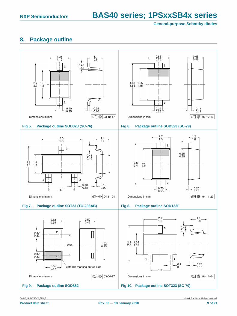
8. Package outline
Fig 5. Package outline SOD323 (SC-76) Fig 6. Package outline SOD523 (SC-79)
Fig 7. Package outline SOT23 (TO-236AB) Fig 8. Package outline SOD123F
Fig 9. Package outline SOD882 Fig 10. Package outline SOT323 (SC-70)
03-12-17Dimensions in mm
0.250.10
0.450.15
2.72.3
1.81.6
0.400.25
1.10.8
1.351.15
1
2
02-12-13Dimensions in mm
1.651.55
1.251.15
0.170.11
0.340.26
0.650.58
0.850.75
1
2
04-11-04Dimensions in mm
0.450.15
1.9
1.10.9
3.02.8
2.52.1
1.41.2
0.480.38
0.150.09
1 2
3
04-11-29Dimensions in mm
1.21.0
0.250.10
3.63.4
2.72.5
0.550.35
0.700.55
1.71.5
1
2
03-04-17Dimensions in mm
0.550.47
0.65
0.620.55
0.500.46
cathode marking on top side
1.020.95
0.300.22
0.300.22
2
1
04-11-04Dimensions in mm
0.450.15
1.10.8
2.21.8
2.22.0
1.351.15
1.3
0.40.3
0.250.10
1 2
3
BAS40_1PSXXSB4X_SER_8 © NXP B.V. 2010. All rights reserved.
Product data sheet Rev. 08 — 13 January 2010 10 of 21
NXP Semiconductors BAS40 series; 1PSxxSB4x seriesGeneral-purpose Schottky diodes
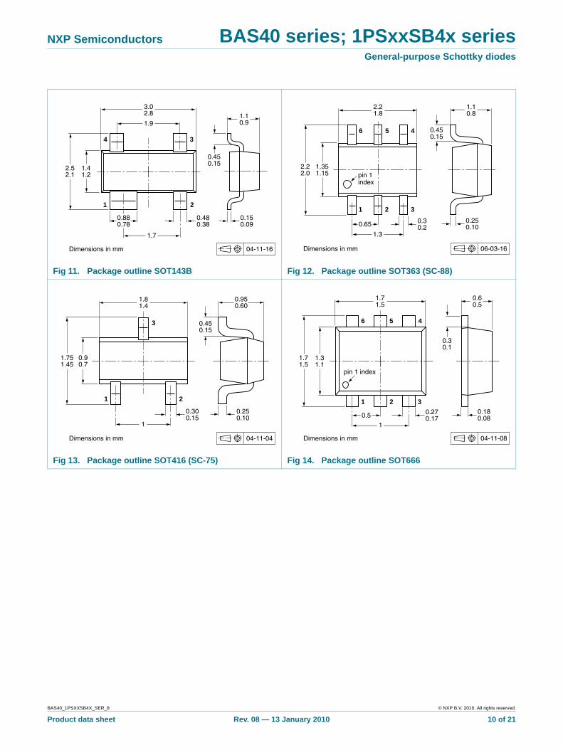
Fig 11. Package outline SOT143B Fig 12. Package outline SOT363 (SC-88)
Fig 13. Package outline SOT416 (SC-75) Fig 14. Package outline SOT666
04-11-16Dimensions in mm
3.02.8 1.1
0.9
2.52.1
1.41.2
1.7
1.9
0.480.38
0.150.09
0.450.15
0.880.78
21
34
06-03-16Dimensions in mm
0.250.10
0.30.2
pin 1index
1.3
0.65
2.22.0
1.351.15
2.21.8
1.10.8
0.450.15
1 32
46 5
04-11-04Dimensions in mm
0.950.60
1.81.4
1.751.45
0.90.7
0.250.10
1
0.300.15
1 2
3 0.450.15
Dimensions in mm 04-11-08
1.71.5
1.71.5
1.31.1
1
0.180.08
0.270.170.5
pin 1 index
1 2 3
456
0.60.5
0.30.1

BAS40_1PSXXSB4X_SER_8 © NXP B.V. 2010. All rights reserved.
Product data sheet Rev. 08 — 13 January 2010 11 of 21
NXP Semiconductors BAS40 series; 1PSxxSB4x seriesGeneral-purpose Schottky diodes
9. Packing information
[1] For further information and the availability of packing methods, see Section 13.
[2] T1: normal taping
[3] T2: reverse taping
Table 9. Packing methodsThe indicated -xxx are the last three digits of the 12NC ordering code.[1]
Type number Package Description Packing quantity
3000 4000 8000 10000
1PS70SB40 SOT323 4 mm pitch, 8 mm tape and reel -115 - - -135
1PS76SB40 SOD323 4 mm pitch, 8 mm tape and reel -115 - - -135
1PS79SB40 SOD523 2 mm pitch, 8 mm tape and reel - - -315 -
4 mm pitch, 8 mm tape and reel -115 - - -135
BAS40 SOT23 4 mm pitch, 8 mm tape and reel -215 - - -235
BAS40H SOD123F 4 mm pitch, 8 mm tape and reel -115 - - -135
BAS40L SOD882 2 mm pitch, 8 mm tape and reel - - - -315
BAS40W SOT323 4 mm pitch, 8 mm tape and reel -115 - - -135
1PS70SB44 SOT323 4 mm pitch, 8 mm tape and reel -115 - - -135
BAS40-04 SOT23 4 mm pitch, 8 mm tape and reel -215 - - -235
BAS40-04W SOT323 4 mm pitch, 8 mm tape and reel -115 - - -135
1PS70SB45 SOT323 4 mm pitch, 8 mm tape and reel -115 - - -135
1PS75SB45 SOT416 4 mm pitch, 8 mm tape and reel -115 - - -135
BAS40-05 SOT23 4 mm pitch, 8 mm tape and reel -215 - - -235
BAS40-05W SOT323 4 mm pitch, 8 mm tape and reel -115 - - -135
1PS70SB46 SOT323 4 mm pitch, 8 mm tape and reel -115 - - -135
BAS40-06 SOT23 4 mm pitch, 8 mm tape and reel -215 - - -235
BAS40-06W SOT323 4 mm pitch, 8 mm tape and reel -115 - - -135
BAS40-07 SOT143B 4 mm pitch, 8 mm tape and reel -215 - - -235
BAS40-07V SOT666 2 mm pitch, 8 mm tape and reel - - -315 -
4 mm pitch, 8 mm tape and reel - -115 - -
BAS40-05V SOT666 2 mm pitch, 8 mm tape and reel - - -315 -
4 mm pitch, 8 mm tape and reel - -115 - -
1PS88SB48 SOT363 4 mm pitch, 8 mm tape and reel; T1 [2] -115 - - -135
4 mm pitch, 8 mm tape and reel; T2 [3] -125 - - -165
BAS40XY SOT363 4 mm pitch, 8 mm tape and reel; T1 [2] -115 - - -135
4 mm pitch, 8 mm tape and reel; T2 [3] -125 - - -165
BAS40_1PSXXSB4X_SER_8 © NXP B.V. 2010. All rights reserved.
Product data sheet Rev. 08 — 13 January 2010 12 of 21
NXP Semiconductors BAS40 series; 1PSxxSB4x seriesGeneral-purpose Schottky diodes
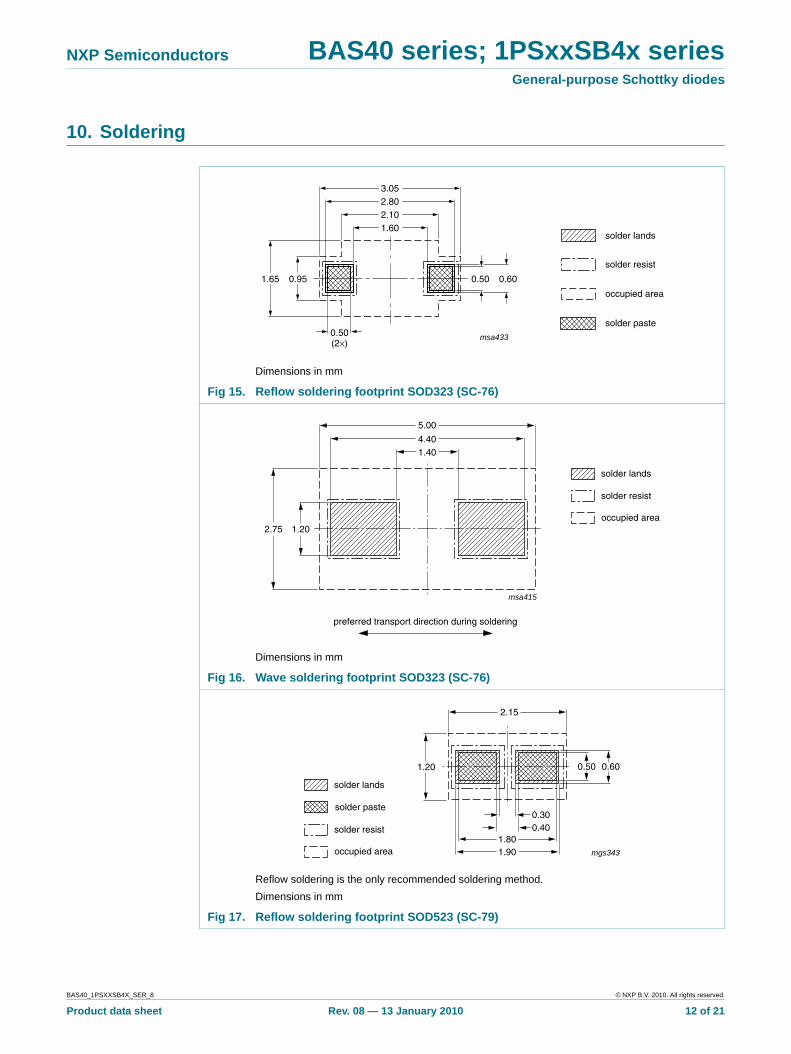
10. Soldering
Dimensions in mm
Fig 15. Reflow soldering footprint SOD323 (SC-76)
Dimensions in mm
Fig 16. Wave soldering footprint SOD323 (SC-76)
Reflow soldering is the only recommended soldering method.
Dimensions in mm
Fig 17. Reflow soldering footprint SOD523 (SC-79)
msa433
1.65
0.50(2×)
2.101.60
2.80
0.60
3.05
0.500.95
solder lands
solder resist
occupied area
solder paste
msa415
1.404.40
5.00
1.202.75
preferred transport direction during soldering
solder lands
solder resist
occupied area
mgs343
1.801.90
0.300.40
0.501.20 0.60
2.15
solder lands
solder resist
occupied area
solder paste
BAS40_1PSXXSB4X_SER_8 © NXP B.V. 2010. All rights reserved.
Product data sheet Rev. 08 — 13 January 2010 13 of 21
NXP Semiconductors BAS40 series; 1PSxxSB4x seriesGeneral-purpose Schottky diodes
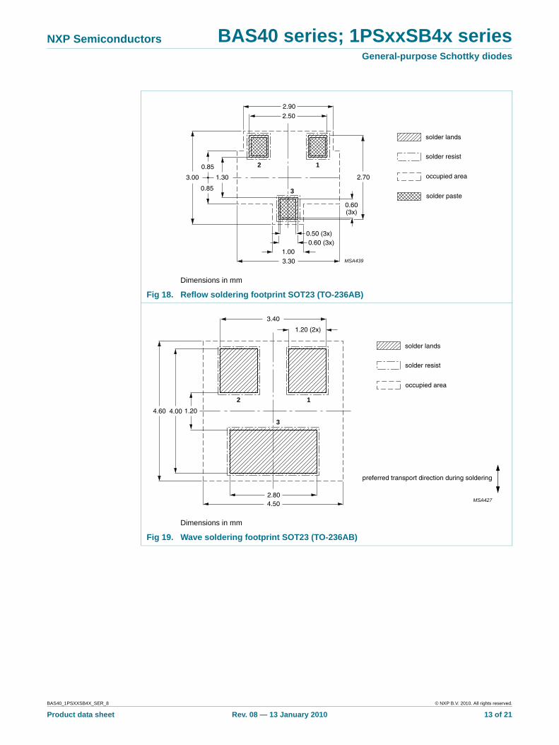
Dimensions in mm
Fig 18. Reflow soldering footprint SOT23 (TO-236AB)
Dimensions in mm
Fig 19. Wave soldering footprint SOT23 (TO-236AB)
MSA439
1.00
0.60(3x)
1.30
12
3
2.50
3.00
0.85
2.70
2.90
0.50 (3x)0.60 (3x)
3.30
0.85
solder lands
solder resist
occupied area
solder paste
MSA427
4.004.60
2.804.50
1.20
3.40
3
2 1
1.20 (2x)
preferred transport direction during soldering
solder lands
solder resist
occupied area

BAS40_1PSXXSB4X_SER_8 © NXP B.V. 2010. All rights reserved.
Product data sheet Rev. 08 — 13 January 2010 14 of 21
NXP Semiconductors BAS40 series; 1PSxxSB4x seriesGeneral-purpose Schottky diodes
Reflow soldering is the only recommended soldering method.
Dimensions in mm
Fig 20. Reflow soldering footprint SOD123F
Reflow soldering is the only recommended soldering method.
Dimensions in mm
Fig 21. Reflow soldering footprint SOD882
1.6
1.6
2.9
4
4.4
1.1 1.22.1
1.1(2×)
solder lands
solder resist
occupied area
solder paste
mbl872
1.30
0.30R = 0.05 (8×) R = 0.05 (8×)
0.60(2×)
0.70(2×)
0.80(2×)0.90
0.30(2×)0.40(2×)0.50(2×)
solder lands
solder resist
occupied area
solder paste
BAS40_1PSXXSB4X_SER_8 © NXP B.V. 2010. All rights reserved.
Product data sheet Rev. 08 — 13 January 2010 15 of 21
NXP Semiconductors BAS40 series; 1PSxxSB4x seriesGeneral-purpose Schottky diodes
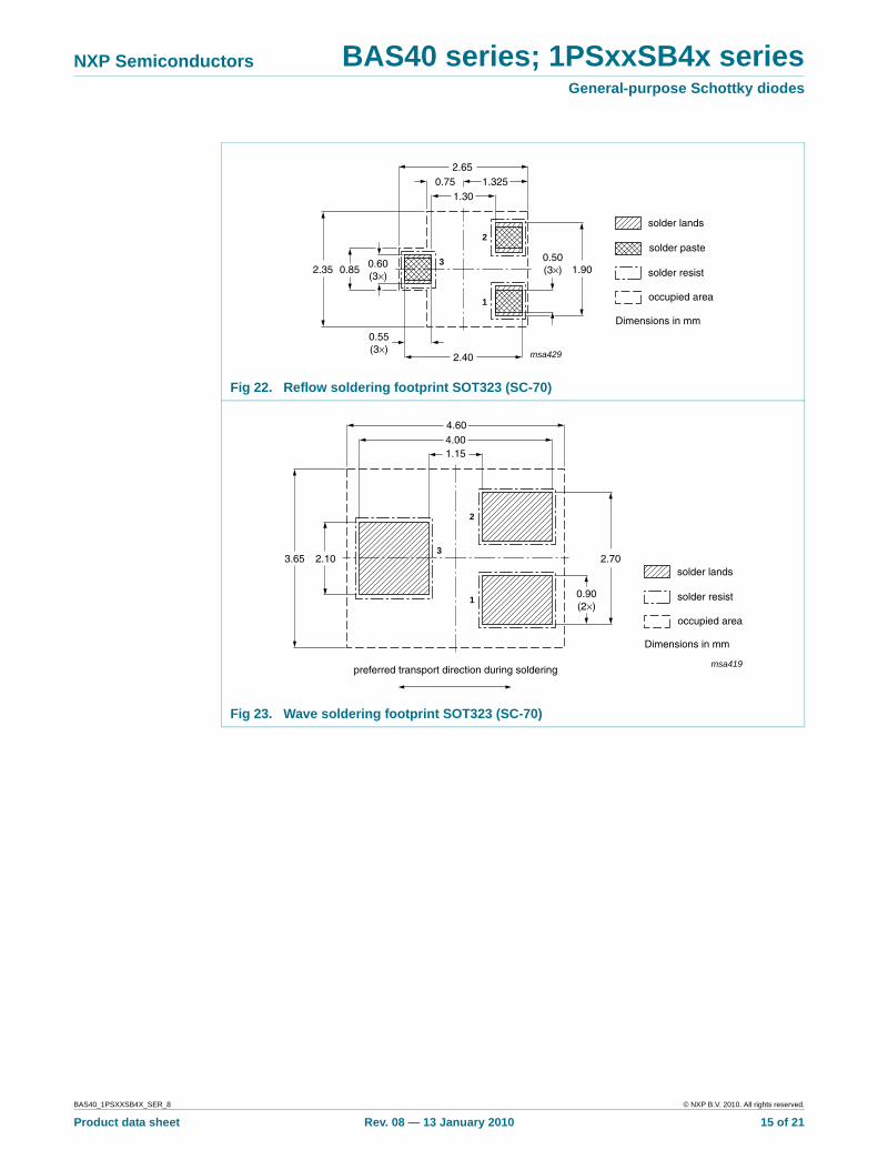
Fig 22. Reflow soldering footprint SOT323 (SC-70)
Fig 23. Wave soldering footprint SOT323 (SC-70)
msa429
0.852.35
0.55(3×)
1.3250.75
2.40
2.65
1.30
3
2
1
0.60(3×)
0.50(3×) 1.90
solder lands
solder resist
occupied area
solder paste
Dimensions in mm
msa419
4.004.60
2.103.65
1.15
2.703
2
10.90(2×)
preferred transport direction during soldering
solder lands
solder resist
occupied area
Dimensions in mm
BAS40_1PSXXSB4X_SER_8 © NXP B.V. 2010. All rights reserved.
Product data sheet Rev. 08 — 13 January 2010 16 of 21
NXP Semiconductors BAS40 series; 1PSxxSB4x seriesGeneral-purpose Schottky diodes
Dimensions in mm
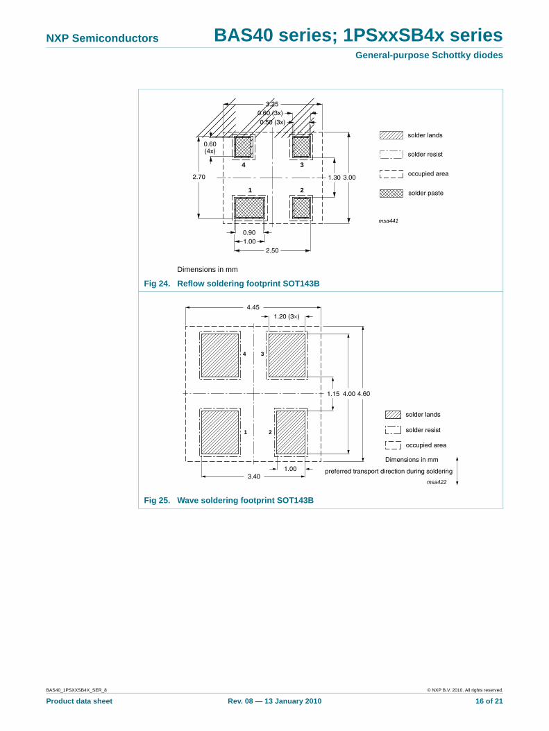
Fig 24. Reflow soldering footprint SOT143B
Fig 25. Wave soldering footprint SOT143B
msa441
0.60(4x)
1.30
2.50
3.002.70
0.50 (3x)0.60 (3x)
3.25
4 3
21
0.901.00
solder lands
solder resist
occupied area
solder paste
msa422
4.00 4.60
1.20 (3×)4.45
1 2
34
1.15
3.401.00 preferred transport direction during soldering
solder lands
solder resist
occupied area
Dimensions in mm

BAS40_1PSXXSB4X_SER_8 © NXP B.V. 2010. All rights reserved.
Product data sheet Rev. 08 — 13 January 2010 17 of 21
NXP Semiconductors BAS40 series; 1PSxxSB4x seriesGeneral-purpose Schottky diodes
Fig 26. Reflow soldering footprint SOT363 (SC-88)
Fig 27. Wave soldering footprint SOT363 (SC-88)
solder lands
solder resist
occupied area
solder paste
sot363_fr
2.65
2.35 0.4 (2×)
0.6(2×)
0.5(4×)
0.5(4×)
0.6(4×)
0.6(4×)
1.5
1.8
Dimensions in mm
sot363_fw
solder lands
solder resist
occupied area
preferred transportdirection during soldering
5.3
1.3 1.3
1.5
0.3
1.5
4.5
2.45
2.5
Dimensions in mm
BAS40_1PSXXSB4X_SER_8 © NXP B.V. 2010. All rights reserved.
Product data sheet Rev. 08 — 13 January 2010 18 of 21
NXP Semiconductors BAS40 series; 1PSxxSB4x seriesGeneral-purpose Schottky diodes
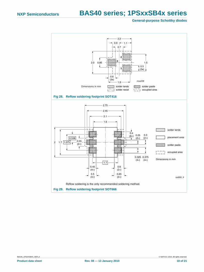
Fig 28. Reflow soldering footprint SOT416
Reflow soldering is the only recommended soldering method.
Fig 29. Reflow soldering footprint SOT666
solder resist occupied areasolder lands solder pasteDimensions in mm
msa438
2.0
0.6(3x)
0.7
1.5
1
2
3
1.1
2.2
0.5(3x)
0.85
0.6
1.9
solder lands
placement area
occupied area
solder paste
sot666_fr
2.75
2.45
2.1
1.6
0.4(6×)
0.55(2×)
0.25(2×)
0.6(2×)
0.65(2×)
0.3(2×)
0.325(4×)
0.45(4×)
0.5(4×)
0.375(4×)
1.72
1.7
1.075
0.538
Dimensions in mm
BAS40_1PSXXSB4X_SER_8 © NXP B.V. 2010. All rights reserved.
Product data sheet Rev. 08 — 13 January 2010 19 of 21
NXP Semiconductors BAS40 series; 1PSxxSB4x seriesGeneral-purpose Schottky diodes
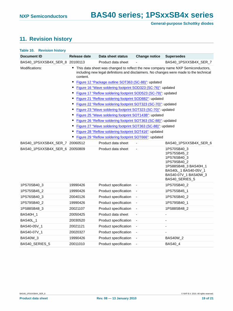
11. Revision history
Table 10. Revision history
Document ID Release date Data sheet status Change notice Supersedes
BAS40_1PSXXSB4X_SER_8 20100113 Product data sheet - BAS40_1PSXXSB4X_SER_7
Modifications: • This data sheet was changed to reflect the new company name NXP Semiconductors, including new legal definitions and disclaimers. No changes were made to the technical content.
• Figure 12 “Package outline SOT363 (SC-88)”: updated
• Figure 16 “Wave soldering footprint SOD323 (SC-76)”: updated
• Figure 17 “Reflow soldering footprint SOD523 (SC-79)”: updated
• Figure 21 “Reflow soldering footprint SOD882”: updated
• Figure 22 “Reflow soldering footprint SOT323 (SC-70)”: updated
• Figure 23 “Wave soldering footprint SOT323 (SC-70)”: updated
• Figure 25 “Wave soldering footprint SOT143B”: updated
• Figure 26 “Reflow soldering footprint SOT363 (SC-88)”: updated
• Figure 27 “Wave soldering footprint SOT363 (SC-88)”: updated
• Figure 28 “Reflow soldering footprint SOT416”: updated
• Figure 29 “Reflow soldering footprint SOT666”: updated
BAS40_1PSXXSB4X_SER_7 20060512 Product data sheet - BAS40_1PSXXSB4X_SER_6
BAS40_1PSXXSB4X_SER_6 20050809 Product data sheet - 1PS70SB40_3 1PS75SB45_2 1PS76SB40_3 1PS79SB40_2 1PS88SB48_3 BAS40H_1BAS40L_1 BAS40-05V_1 BAS40-07V_1 BAS40W_3 BAS40_SERIES_5
1PS70SB40_3 19990426 Product specification - 1PS70SB40_2
1PS75SB45_2 19990426 Product specification - 1PS75SB45_1
1PS76SB40_3 20040126 Product specification - 1PS76SB40_2
1PS79SB40_2 19990426 Product specification - 1PS79SB40_1
1PS88SB48_3 20021107 Product specification - 1PS88SB48_2
BAS40H_1 20050425 Product data sheet - -
BAS40L_1 20030520 Product specification - -
BAS40-05V_1 20021121 Product specification - -
BAS40-07V_1 20020327 Product specification - -
BAS40W_3 19990426 Product specification - BAS40W_2
BAS40_SERIES_5 20011010 Product specification - BAS40_4
BAS40_1PSXXSB4X_SER_8 © NXP B.V. 2010. All rights reserved.
Product data sheet Rev. 08 — 13 January 2010 20 of 21
NXP Semiconductors BAS40 series; 1PSxxSB4x seriesGeneral-purpose Schottky diodes
12. Legal information
12.1 Data sheet status
[1] Please consult the most recently issued document before initiating or completing a design.
[2] The term ‘short data sheet’ is explained in section “Definitions”.
[3] The product status of device(s) described in this document may have changed since this document was published and may differ in case of multiple devices. The latest product status information is available on the Internet at URL http://www.nxp.com.
12.2 Definitions
Draft — The document is a draft version only. The content is still under internal review and subject to formal approval, which may result in modifications or additions. NXP Semiconductors does not give any representations or warranties as to the accuracy or completeness of information included herein and shall have no liability for the consequences of use of such information.
Short data sheet — A short data sheet is an extract from a full data sheet with the same product type number(s) and title. A short data sheet is intended for quick reference only and should not be relied upon to contain detailed and full information. For detailed and full information see the relevant full data sheet, which is available on request via the local NXP Semiconductors sales office. In case of any inconsistency or conflict with the short data sheet, the full data sheet shall prevail.
12.3 Disclaimers
General — Information in this document is believed to be accurate and reliable. However, NXP Semiconductors does not give any representations or warranties, expressed or implied, as to the accuracy or completeness of such information and shall have no liability for the consequences of use of such information.
Right to make changes — NXP Semiconductors reserves the right to make changes to information published in this document, including without limitation specifications and product descriptions, at any time and without notice. This document supersedes and replaces all information supplied prior to the publication hereof.
Suitability for use — NXP Semiconductors products are not designed, authorized or warranted to be suitable for use in medical, military, aircraft, space or life support equipment, nor in applications where failure or malfunction of an NXP Semiconductors product can reasonably be expected to result in personal injury, death or severe property or environmental
damage. NXP Semiconductors accepts no liability for inclusion and/or use of NXP Semiconductors products in such equipment or applications and therefore such inclusion and/or use is at the customer’s own risk.
Applications — Applications that are described herein for any of these products are for illustrative purposes only. NXP Semiconductors makes no representation or warranty that such applications will be suitable for the specified use without further testing or modification.
Limiting values — Stress above one or more limiting values (as defined in the Absolute Maximum Ratings System of IEC 60134) may cause permanent damage to the device. Limiting values are stress ratings only and operation of the device at these or any other conditions above those given in the Characteristics sections of this document is not implied. Exposure to limiting values for extended periods may affect device reliability.
Terms and conditions of sale — NXP Semiconductors products are sold subject to the general terms and conditions of commercial sale, as published at http://www.nxp.com/profile/terms, including those pertaining to warranty, intellectual property rights infringement and limitation of liability, unless explicitly otherwise agreed to in writing by NXP Semiconductors. In case of any inconsistency or conflict between information in this document and such terms and conditions, the latter will prevail.
No offer to sell or license — Nothing in this document may be interpreted or construed as an offer to sell products that is open for acceptance or the grant, conveyance or implication of any license under any copyrights, patents or other industrial or intellectual property rights.
Export control — This document as well as the item(s) described herein may be subject to export control regulations. Export might require a prior authorization from national authorities.
Quick reference data — The Quick reference data is an extract of the product data given in the Limiting values and Characteristics sections of this document, and as such is not complete, exhaustive or legally binding.
12.4 TrademarksNotice: All referenced brands, product names, service names and trademarks are the property of their respective owners.
13. Contact information
For more information, please visit: http://www.nxp.com
For sales office addresses, please send an email to: [email protected]
Document status[1][2] Product status[3] Definition
Objective [short] data sheet Development This document contains data from the objective specification for product development.
Preliminary [short] data sheet Qualification This document contains data from the preliminary specification.
Product [short] data sheet Production This document contains the product specification.

NXP Semiconductors BAS40 series; 1PSxxSB4x seriesGeneral-purpose Schottky diodes
© NXP B.V. 2010. All rights reserved.
For more information, please visit: http://www.nxp.comFor sales office addresses, please send an email to: [email protected]
Date of release: 13 January 2010
Document identifier: BAS40_1PSXXSB4X_SER_8
Please be aware that important notices concerning this document and the product(s)described herein, have been included in section ‘Legal information’.
14. Contents
1 Product profile . . . . . . . . . . . . . . . . . . . . . . . . . . 11.1 General description . . . . . . . . . . . . . . . . . . . . . 11.2 Features . . . . . . . . . . . . . . . . . . . . . . . . . . . . . . 21.3 Applications . . . . . . . . . . . . . . . . . . . . . . . . . . . 21.4 Quick reference data . . . . . . . . . . . . . . . . . . . . 2
2 Pinning information. . . . . . . . . . . . . . . . . . . . . . 2
3 Ordering information. . . . . . . . . . . . . . . . . . . . . 5
4 Marking . . . . . . . . . . . . . . . . . . . . . . . . . . . . . . . . 6
5 Limiting values. . . . . . . . . . . . . . . . . . . . . . . . . . 6
6 Thermal characteristics . . . . . . . . . . . . . . . . . . 7
7 Characteristics. . . . . . . . . . . . . . . . . . . . . . . . . . 7
8 Package outline . . . . . . . . . . . . . . . . . . . . . . . . . 9
9 Packing information . . . . . . . . . . . . . . . . . . . . 11
10 Soldering . . . . . . . . . . . . . . . . . . . . . . . . . . . . . 12
11 Revision history. . . . . . . . . . . . . . . . . . . . . . . . 19
12 Legal information. . . . . . . . . . . . . . . . . . . . . . . 2012.1 Data sheet status . . . . . . . . . . . . . . . . . . . . . . 2012.2 Definitions. . . . . . . . . . . . . . . . . . . . . . . . . . . . 2012.3 Disclaimers . . . . . . . . . . . . . . . . . . . . . . . . . . . 2012.4 Trademarks. . . . . . . . . . . . . . . . . . . . . . . . . . . 20
13 Contact information. . . . . . . . . . . . . . . . . . . . . 20
14 Contents . . . . . . . . . . . . . . . . . . . . . . . . . . . . . . 21