barc newsletter
TRANSCRIPT


B A R C N E W S L E T T E R
In the Forthcoming Issue
1. “Cyber-security, Personnel Tracking and Surveillance Solution”D.K. Dixit et al.
2. Friction Stir Welding of Al alloysN.S. Kumbhar et al.
3. Ground Response Analysis and Behavior of Single Pile in LiquefiedSoils during EarthquakeV.S. Phanikanth et al.
4. Precision-Micro-Nano EngineeringV.K. Suri et al.
5. Radiation Processing of Temperate Fruits of Kashmir ValleyP.R. Hussain et al.
6. Composite Polyamide Reverse Osmosis(RO) Membranes-RecentDevelopments and Future DirectionsA.K. Ghosh et al.
7. Matrix-assisted laser Desorption/Ionization Time-of-Flight MassSpectrometry for Biomolecular ResearchT. Jayasekharan and N.K. Sahoo

B A R C N E W S L E T T E R
ISSUE NO. 320 I MAY - JUNE 2011 I I
Contents
Research Articles
Thermal and Stress Analyses of Oblong Shaped Metallic Melter 1
S.M.Thorve et al.
Analytical Performance of Refractometry in Quantitative Estimation of Isotopic 7
Concentration of Heavy Water in Nuclear Reactor
K. Dhole et al.
Characterization of High Level Liquid Waste Generated from Reprocessing of 12
Power Reactor Spent Fuel
B.S.Tomar et al.
Technology Development Articles
Development of High Temperature Thermoelectric Materials and Fabrication of Devices 17
Deep Prakash et al.
Development and Fabrication of Superconducting Hybrid Cable-In-Conduit-Conductor 26
(CICC) for indigenous Fusion Programme
A.K. Singh et al.
Feature Articles
Multi-Detector Environmental Radiation Monitor with Multichannel Data 31
Communication for Indian Environmental Radiation MOnitoring Network (IERMON)
M.D. Patel et al.
Mapping Interfaces in Magnetic Thin Films with Neutron Reflectometry 35
Saibal Basu and Surendra Singh
News & Events
• India and CERN: Visions for Future Collaboration 44
• Report on the Seminar “Nanotechnology and Its Applications” 45
• National Technology Day Celebration at BARC : a report 46
BARC Scientists Honoured

B A R C N E W S L E T T E R
II I ISSUE NO. 320 I MAY - JUNE 2011
Editorial Committee
Chairman
Dr. V. Venugopal,
Director, RC&I Group
Edited by
Dr. K. Bhanumurthy
Head, SIRD
Associate Editors for this issue
Dr. Madangopal Krishnan, MSD
Dr. C. Srinivas, PsDD
Members
Dr. V. Venugopal, RC&I Group
Mr. C.S.R. Prasad,ChTD
Dr. D.N. Badodkar, DRHR
Dr. A.P. Tiwari, RCnD
Dr. Madangopal Krishnan, MSD
Dr. A.K. Tyagi, ChD
Dr. P.V. Varde, RRSD
Dr. S.M. Yusuf, SSPD
Mr. Avaneesh Sharma, RED
Dr. C. Srinivas, PsDD
Dr. G. Rami Reddy, RSD
Dr. S.K. Mukherjee, FCD
Mr. G. Venugopala Rao, APPD
Dr. A. Vinod Kumar, EAD
Dr. Anand Ballal, MBD
Dr. K. Bhanumurthy, SIRD
Dr. S.C. Deokattey, SIRD
From the Editor’s Desk ...
The Founder’s Day Special Issue of the BARC Newsletter
will be released on the occasion of Founder’s Day, in
October 2011. As was done in the previous year, the
issue will be printed only in the CD format. This year,
we have hosted a web link on the homepage of BTS.
DAE and other award winners are invited to login to the
website and upload their papers directly. This would save
a lot of time and effort and would help us in bringing
out the Special Issue on time. Kindly note, that the last
date for uploading all award winning papers for this
issue, is 31st July, 2011.
This issue carries seven articles in various research
categories and two important R&D contributions from
BARC are of general interest. One is the work on an
oblong shaped metallic melter, which would enhance
the melter throughput for vitrification of high level waste.
The other is the development and fabrication of Cable-
In-Conduit-Conductor (CICC). This superconducting high-
grade multifilamentary wire, would be used for our
indigenous fusion programme.
Looking forward to contributions from all the award
winners, on or before 31st July, 2011.
Dr. K. Bhanumurthy
On behalf of the Editorial Committee

ISSUE NO. 320 I MAY - JUNE 2011 I 1
B A R C N E W S L E T T E R RESEARCH ARTICLE
Thermal and Stress Analyses of Oblong Shaped
Metallic Melter
S.M. Thorve, G. Sugilal and K.N.S. Nair
Technology Development Division
Abstract
Induction heated metallic melter with a circular cross section is presently employed in the Waste Immobilization
Plant at Trombay for high level liquid waste vitrification. In order to enhance melter throughput, an oblong
shaped metallic melter is being developed in the Nuclear Recycle Group. As part of the safety analysis,
finite element based thermal and stress analyses of the oblong shaped metallic melter have been carried
out. Based on the thermal analysis, it is recommended to directly heat the process vessel, to obtain higher
glass pool temperature. Present study also shows that the top supported design results in a creep strain rate
of 0.02 % per hour at the melter bottom, which restricts the melter life to 2000 hours. Therefore, a bottom
supported design is recommended to reduce the creep strain rate and process pot deformation.
Introduction
Induction heated metallic melter has been
successfully employed in the Waste Immobilization
Plant (WIP) at Trombay for high level liquid waste
vitrification. A multi-zone induction heating system
is used for heating an inconel susceptor, which
surrounds the process pot. Thermal radiations from
the susceptor in turn heat the inconel process pot
in which the incoming waste stream and glass
forming additives undergo boiling, drying,
calcination and melting to form the vitrified product.
At present, a process pot with circular cross section
having a diameter of 300 mm is used in WIP
Trombay. Although the present metallic melter has
several advantages, its main limitation is the limited
throughput. In order to enhance the melter capacity,
an oblong shaped metallic melter is being developed
in the Nuclear Recycle Group, based on the concept
of elliptically-shaped metallic melter reported in
literature.
As a part of the safety analysis, the thermal stresses
and the deflections as well as sustained stresses in
the oblong shaped metallic melter were computed
using finite element technique. This analysis was
carried out in two parts: (i) thermal analysis to obtain
temperature distribution in various components of
melter and in glass pool, and (ii) stress analysis of
both process pot and succeptor of the melter.
Description of Oblong Shaped Metallic
Melter
The metallic melter has two main vessels – a
susceptor and a process pot. Fig. 1 shows the
geometric details of melter vessels1. The susceptor
is the outer vessel of the melter and made of
15 mm thick inconel 690 plates. Lower portion of
the susceptor vessel is surrounded by electric
induction coils. The process pot is an inner vessel of
melter in which vitrification of high level waste takes
place. It contains a glass pool during normal
operation and has a drain pipe (freeze valve) at the
bottom to drain out molten glass in to a canister.
Process pot has 15 mm thickness and is made of

2 I ISSUE NO. 320 I MAY - JUNE 2011
B A R C N E W S L E T T E RRESEARCH ARTICLE
inconel 690. Both the susceptor and process pot
are supported on respective flanges and free to
expand downwards.
Finite Element Analysis
Oblong shaped melter was analyzed using the finite
element software NISA. Two types of three-
dimensional solid elements - 8 noded hexahedron
and 6 noded wedge elements were used for the
analysis3. Finite element model of melter is made
up of 55624 elements and 71914 nodes. Fig. 2
shows the finite element model of oblong shaped
metallic melter.
Thermal Analysis
Thermal analysis of melter was performed using finite
element method to obtain accurate temperature
distribution in melter components as well as molten
glass pool2. All three modes of heat transfer were
considered in the analysis and implemented by
applying appropriate boundary conditions3. This
analysis was carried out for the following three
different cases:
Case 1: Initial heating condition
In case 1, simulation of green heating of the empty
melter was performed for verification of finite
element model. During the green heating
experiments, initial heating of the oblong shaped
melter were carried out with empty process pot and
temperature distributions across various parts of
melter were measured employing thermocouples
during this test.
Case 2: Normal operation condition
In case 2, heat transfer analysis was completed for
a normal operation condition, wherein a cold cap
of low thermal conductivity is formed at the surface
of glass pool. The liquid glass is assumed to be
filled up to a height of 275 mm with a cold cap of
20 mm.
Case 3: Soaking condition
In case 3, thermal analysis was done for soaking
condition which corresponds to product
homogenization. In this case, process pot contains
a vitrified product ready for draining in to a canister.
Fig. 1: Geometric details of oblong shapedmetallic melter
Fig. 2: Finite element model of oblong shapedmetallic melter

ISSUE NO. 320 I MAY - JUNE 2011 I 3
B A R C N E W S L E T T E R RESEARCH ARTICLE
Stress Analysis
The objective of this analysis was to calculate the
stress distribution pattern in the melter due to
sustained loads (self weight, weight of glass, etc)
and thermal loads. Susceptor and process pot are
each supported at four locations on their respective
flanges. Appropriate displacement boundary
conditions were applied on the finite element model
at support locations for this analysis4. For thermal
stress analysis, nodal temperatures required as input
boundary conditions were directly read from output
result file of thermal analysis.
Results
Results of Thermal Analysis
Temperature distributions in various parts of oblong
shaped metallic melter were computed and
maximum temperatures in melter vessels obtained
for case 1 of the thermal analysis are summarized
in Table 1. These results were used for model
validation. Table 2 gives a comparison of
experimental results and analysis results. The model
predictions are in good agreement with experimental
results and thereby, confirm the accuracy of finite
element model and applied boundary conditions.
An additional run for case 1 was carried out with
increased power to induction coils surrounding the
susceptor such that the susceptor temperature profile
increased by about 100 oC. Maximum temperatures
obtained for different cases are compared in Table
3. Fig. 3 shows the temperature distribution in the
melter components for revised case 1 with increased
power level.
Results of Stress Analysis
The stresses in melter due to sustained loads (self
weight and weight of glass) are summarized in Table
4. Fig. 4 shows the vonmises stress plots in susceptor
and process pot.
Allowable stress intensity mentioned in Table 4 does
not take into consideration damage due to creep
phenomenon which will be quite significant at high
temperatures. As the melter vessels experience high
temperatures, creep strain rate and creep rupture
life are important parameters which need to be
evaluated5. These parameters were evaluated, based
on the available creep curves at various
temperatures. These results are shown for melter
components in Table 5. The creep rupture life of
process pot is the lowest and hence will govern
Maximum Temperature
Component RevisedCase 1 Case 2 Case 3
Susceptor 1131 oC 1131 oC 1131 oC
Process Pot 972 oC 866.5 oC 998.4 oC
Liquid glass - 849.3 oC 991.3 oC
Maximum Temperature of Process Pot
From Thermal analysis From Experiment
876.2 oC 878 oC
Table 1: Maximum temperatures for Case 1 ofthermal analysis
Table 2: Comparison of experimental and thermalanalysis results
Component Maximum Temperature
Susceptor 1031 oC
Process Pot 876.2 oC
Component Maximum Stress AllowableIntensity Stress Intensity
Susceptor 1.94 N/mm2 43 N/mm2
Process Pot 2.0 N/mm2 43 N/mm2
Table 4: Stresses due to sustained loads
Table 3: Maximum temperatures for revised Case1, Case 2 & Case 3 of thermal analyses
Component Creep Strain Rate CreepRupture Life
Susceptor < 10-5 %/hr > 105 hours
Process Pot 0.02 %/hr 2000 hours
Table 5: Creep strain rate and creep rupture life ofmelter

4 I ISSUE NO. 320 I MAY - JUNE 2011
B A R C N E W S L E T T E RRESEARCH ARTICLE
Fig. 3: Temperature distribution in melter for revised Case 1 of thermal analysis
Fig. 4: Vonmises stress plot in susceptor due to sustained loads

ISSUE NO. 320 I MAY - JUNE 2011 I 5
B A R C N E W S L E T T E R RESEARCH ARTICLE
melter rupture life. Thus the creep rupture life of
melter is 2000 hours3.
Thermal stress analysis of melter was done for
soaking condition as the maximum temperature in
melter occurs during soaking condition (Case 3 of
thermal analysis). Maximum thermal deflections and
thermal stresses in melter thus obtained are
summarized in Table 6. Fig. 5 shows the thermal
stress plots in susceptor and process pots.
Calculation of Fatigue Life
Maximum thermal stress in susceptor occurs at the
junction of vessel with bottom pipe. Similarly,
maximum thermal stress in process pot occurs at
the junction of vessel with drain pipe (freeze valve).
These peak stresses are due to geometric
discontinuity in these regions5. Thermal stresses are
secondary in nature and will cause failure by fatigue
after some cycles. The fatigue life calculated for
Fig. 5: Thermal stress plot in susceptor & process pot
Component Maximum thermal deflection Maximum
Horizontal (at support bolts) Vertical Thermal Stress
Susceptor 4.01 mm 20.54 mm 976.3 N/mm2
Process Pot 5.09 mm 28.31 mm 213.6 N/mm2
Table 6: Maximum thermal deflections and thermal stresses in melter

6 I ISSUE NO. 320 I MAY - JUNE 2011
B A R C N E W S L E T T E RRESEARCH ARTICLE
susceptor and process pot is 70 cycles and 2 x 10⁶
cycles respectively6.
Conclusions
The results of thermal and stress analyses lead to
the following conclusions:
(i) Thermal analyses carried out shows that
the succeptor temperature should exceed
1100 oC in order to obtain the glass pool
temperature greater than 950 oC during
soaking. Continuous exposure to temperatures
greater than 1050 oC is undesirable for
inconel 690. Therefore, it is recommended
to design a melter without susceptor so that
induction coils can directly heat the process
pot. Thus, it will be possible to maintain
maximum metal temperature under 1050 oC.
(ii) Oblong bolt holes have been suggested on
the flanges of susceptor and process pot
instead of circular bolt holes in order to take
care of horizontal thermal deflections at
supporting locations.
(iii) Fatigue life of melter has been calculated to
be approximately 70 cycles. Creep rupture
life has been calculated as 2000 hours.
(iv) Present study shows that the top supported
design results in a creep strain rate of 0.02 %
per hour at the melter bottom, which restricts
the melter life to 2000 hours. Therefore, a
bottom supported design is recommended
to reduce the creep strain rate and process
pot deformation.
References
1. R. K. Gupta, A. K. Singh, S. B. Patil, J. Jha, K.
K. Haldar, S. D. Misra. “Engineering and
manufacture of oblong shaped metallic melter
for enhancing engineering throughputs”. ENC
2010 Transactions ISBN-978-92-95064-09-6,
May 30 to June 02, 2010, Spain.
2. F. P. Incropera & D. P. Dewitt. Fundamentals of
Heat and Mass Transfer. Wiley India Ltd., 2006
3. Shailesh. M. Thorve, G. Sugilal, K. N. S. Nair.
“Thermal and Stress Analysis of Oblong Shaped
Melter”. BARC Internal Report, 2011.
4. Engineering Mechanics Research Corporation.
User’s Manual for NISA Display III and Heat III,
1998.
5. J. F. Harvey. Theory and Design of Pressure
Vessels, CBS Publishers, 2001.
6. ASME Boiler and Pressure Vessel Code, Section
III, Div 1, Appendix 1, 2001.

ISSUE NO. 320 I MAY - JUNE 2011 I 7
B A R C N E W S L E T T E R RESEARCH ARTICLE
Analytical Performance of Refractometry in
Quantitative Estimation of Isotopic
Concentration of Heavy Water in Nuclear Reactor
K. Dhole, S. Ghosh, A. Datta, M. K. Tripathy and H. Bose
Research Reactor Services Division
and
M. Roy and A. K. TyagiChemistry Division
Abstract
The method of refractometry has been investigated for the quantitative estimation of isotopic concentration
of D2O (heavy water) in a simulated water sample. Viability of Refractometry as an excellent analytical
technique for rapid and non-invasive determination of D2O concentration in water samples has been
demonstrated. Temperature of the samples was precisely controlled to eliminate effect of temperature
fluctuation on refractive index measurement. Calibration performance by this technique exhibited reasonable
analytical response over a wide range (1-100%) of D2O concentration.
Keywords: D2O; Heavy Water; Refractometry; Refractive Index; RI.
Introduction
Heavy water (D2O) is used as a neutron moderator
and coolant in Presssurised Heavy Water Reactors
(PHWRs) and research reactors. The degradation of
heavy water concentration in a reactor core results
in loss of reactivity. Thus, a very accurate analysis
of isotopic purity of heavy water in the core is
necessary from reactivity point of view. Infrared
absorption method is applied for this purpose
because the method is very accurate and highly
reproducible. However, infrared method has
generally been applied to the isotopic analysis of
heavy water with considerable success particularly
at high and low D2O concentrations. Since the
characteristic absorption bands are very intense, the
concentration ranges analyzable by the use of
respective bands through infrared technique are
limited to narrow regions at either end of D2O
concentration range. For analysis in the broad
intermediate concentration range which includes
heavy water samples from intermediate stages of a
production or upgradation facility, heavy water
leakages from the different systems of PHWRs and
research reactors, bed effluent of columns in the
process of deuterisation and inventory samples, the
method of refractometry can be employed.
Refractometric method may be used for rapid
analysis of D2O [1-5] over the entire range from
1% to100 % D2O. Temperature of the sample and
wavelength of light used are the most common
experimentally controllable variables, that affect a
refractive index (RI) measurement of liquid. For many
liquids the index of refraction decreases by
approximately 0.0005 for every 1°C increase in
temperature. However, the variation for water is only
about “0.0001/°C. In order to achieve a reasonable
analytical reproducibility in the application of
refractometry, a substantial importance has been
given here to the control of temperature fluctuations.

8 I ISSUE NO. 320 I MAY - JUNE 2011
B A R C N E W S L E T T E RRESEARCH ARTICLE
In this study, weight percentage (wt.%) and mole
percentage (mol%) concentration-variations, both
have been used, to build a calibration model over
the range of 1-100%.
Experimental
Sample preparation
A total of 13 samples were prepared for the
measurements over the concentration range of 1
to 100 % D2O. The reference standard D
2O of 99.96
wt.% ( + 0.01 ) was obtained from Research
Reactor Services Division, BARC, Trombay and
appropriate amount of H2O was mixed with standard
D2O in the preparation of samples. To minimize
analytical error in sample preparation, all the samples
were prepared in significant volume using 50ml
conical flask. Ultra pure water (>18 MΩ cm-1,
Milli-Q) was used throughout the whole experiment.
Measurement of Refractive Index and data
processing
RI measurements were done on a digital
refractometer, RFM870 (Bellingham + Stanley Ltd.,
Longfield Road, Tunbridge Wells, Kent TN2 3EY, UK)
equipped with artificial sapphire prism and Pt100
sensor (for monitoring sample temperature, Fig. 1).
Each RI measurement was done using the
temperature control system by placing a small
amount of liquid (~0.5 ml) onto the prism plate
dish. All refractive index (20ηD) values correspond to
the D line of sodium ( λ = 589.3 nm) at a particular
temperature (20°C). Refractometer was conveniently
calibrated with three standard liquids supplied by
B+S ltd., UK, such as BSDC & OILDC, BSLP & OILLP
and AG refractometer calibration fluids with RI values
(20ηD) =1.52256 + 0.000074, (20η
D) =1.46990 +
0.00074 and (20ηD) =1.33659 + 0.000026
respectively. In order to build a calibration model
over the range of 1 % to 100 % D2O, concentrations
in terms of wt.% and mol% both were considered.
RI (20ηD) data were imported into ORIGIN (Origin
Lab Corporation, One Roundhouse Plaza, USA) along
with data for wt.% and mol% concentration-
variations before the calibration was performed.
The experimentally determined RI (20ηD) values for
D2O-H
2O mixtures at 20°C were then correlated to
the polynomial form of refractive index equation. A
total of 13 RI (20ηD) measurements from 13 samples
were divided into 7 RI data for calibration and 6 RI
data for the prediction set serving as a validation
set.
Results and Discussion
Features for refractometric measurement
The refractive index of liquids changes significantly
with temperature. It is important that the temperature
of a sample is to be constant throughout its mass
before an accurate reading can be taken. The
Fig.1: RFM870 Refractometer (Bellingham andStanley Ltd., Longfield Road, Tunbridge Wells,Kent TN2 3EY, UK).

ISSUE NO. 320 I MAY - JUNE 2011 I 9
B A R C N E W S L E T T E R RESEARCH ARTICLE
sapphire prism together with the sample dish and
lid over it can help for achieving optimal thermal
conductivity and low-volume containment of the
sample which enables rapid thermal equilibration
with the prism surface and subsequent temperature
stability of the sample for the duration of the
reading. A highly stable optical system coupled with
a thermally self-regulating detection system, with
enhanced resolution, provides accurate reading in
the shortest possible time. An intelligent electronic
control system coupled with a twin-probe sensor,
which accurately pinpoints the prism surface
temperature, enables the system to achieve and
maintain the sample at the prescribed temperature.
A powerful system of Peltier devices and thermal
insulation ensures rapid attainment of sample target
temperature. A separate multiple probe system
continuously monitors the internal environment of
the instrument and actively compensates any thermal
fluctuations to optical and detector components.
Performance of the instrument is described in
Table 1.
Quantitative calibration
Fig. 2 shows the behavior of the refractive index
property of the samples prepared with various
concentrations in terms of wt.%.
Interestingly, the experimentally determined RI (20ηD)
values for D2O-H
2O mixtures at 20°C do follow
polynomial relation of higher order with wt.%
variation, instead of linear relation. As observed from
experimental results, data could be correlated to the
following form 20ηD (D
2O-H
2O mix)/ 20η
D (H
2O)
=a0+a
1x+a
2x2 where x is the weight percentage of
D2O in D
2O-H
2O mixture. This equation is very much
useful particularly in the quantitative estimation of
wt.% of D2O where the values of coefficients a
0, a
1
and a2 are computed as 1.0 + 6.17592x10⁻⁶,
-2.98051×10 -5 + 2.67782×10 -7 and
-4.42277×10⁻⁸ + 2.56381×10⁻⁹ respectively.
However, for analytical purpose, we need to know
the potential of each of the calibration method.
Therefore, both wt.% and mol% concentration-
variations are used in the calibration model for their
assessment purpose. First, wt.% variation was used
to build a quantitative calibration model. The
refractive index was used to correlate with the
concentration of D2O by linear regression method.
The resulting calibration equation was
y (RI: 20ηD) = -4.5695×10⁻⁵ × x (wt.%) + 1.33309
with the correlation coefficient (R2) of 0.99826. Then
the resulting standard error of calibration (SEC) was
calculated. Using the refractive index data in the
Table 1: Performance of Refractometer
Calibration method SEC SEP
wt. % 1.32 0.98
mol% 0.31 0.25
Fig. 2: Behavior of Refractive index for wt% variation.
Model RFM870 Refractive Index
Range minimum 1.30
Range maximum 1.70
Display resolution 0.00001
Repeatability + 0.00002
Temperature stability + 0.05 °C
Table 2: Calibration results using wt% and mol%

10 I ISSUE NO. 320 I MAY - JUNE 2011
B A R C N E W S L E T T E RRESEARCH ARTICLE
prediction set, the standard error of prediction (SEP)
was also calculated. The results are summarized in
Table 2.
The achieved SEC and SEP were 1.32 and 0.98
wt.%, respectively. In Fig. 3(a), filled and open
circles represent the calibration and prediction data,
respectively. As shown in this figure, when wt.%
was used, a fairly good correlation was achieved
between the reference and the predicted
concentrations. In order to ensure the calibration
performance, mol%- variation method has also been
accounted. Hence, the cross-validation was
performed, in the same way as considered in wt.%-
variation method, by dividing the data set into two
segments to assign 54% of data into calibration,
and the other 46% of data for validation.
Fig. 3: Concentration correlation plot using (a) wt.%and (b) mol% variations. Filled and open circlesrepresent the calibration and prediction datarespectively
The resulting calibration equation was y
(RI: 20ηD) = -4.57319×10⁻⁵ × x (mol %) + 1.33302
with the correlation coefficient (R2) of 0.9999. The
plot in Fig. 3 (b) shows the correlation between
reference concentrations and RI measurements. Here
also, filled and open circles represent the calibration
and prediction data, respectively. The calibration and
prediction data correlate very well with the reference
data. The resulting SEC and SEP are summarized in
Table 2.
The concentrations of D2O in the prediction data
set were predicted with a SEP of 0.25 obtained in
mol%-variation method. The resulting SEP is
considerably improved compared to 0.98 obtained
in wt%-variation method. Both SEC and SEP are
significantly improved when mol%-variation
method has been employed. The achieved SEP is
acceptable from the viewpoint of rapid isotopic
analysis of D2O concentration in Nuclear Reactor.
Conclusion
The method of Refractometry for the analysis of
D2O has been studied, to monitor the concentration
over the entire range from 1 % to 100 % D2O. The
method is extremely important for an alternative
quantitative analysis because of its simplicity and
very small volume of sample requirement. The
measurement of refractive index property with the
application of temperature control has been utilized
here, for the purpose of the quantitative estimation
of isotopic concentration of D2O in nuclear reactor.
The present study indicates that the polynomial form
of refractive index equation for wt.% variation
method and the calibration model based on linear
regression analysis for mol% variation method are
the most suitable ways to predict D2O concentration
accurately in the application of refractometry.
However, there are several issues yet to be addressed.
The prime issue is the difficulty for isotopic analysis

ISSUE NO. 320 I MAY - JUNE 2011 I 11
B A R C N E W S L E T T E R RESEARCH ARTICLE
of D2O through this method, with increase in
impurity content (cationic/anionic) and turbidity in
the accumulations of heavy water from different
locations at the site during reactor operation. Here,
standard D2O and ultra pure H
2O were used
throughout this study in the preparation of samples
i.e. conductivity of the samples prepared is kept
very low. This is directly related with the refractive
index of a medium because of the accompanying
change in density. Therefore, the behaviour of index
of refraction for heavy water samples containing
dissolved solids, oil, organic matters etc. needs to
be explored.
Acknowledgement
The authors are thankful to Mr. R. C. Sharma, Head
RRSD, BARC for his keen interest and constant
encouragement in the work.
References
1. G. P. Baxter, L. L. Burgess and H. W. Daudt,
J. Am. Chem. Soc., 33 (6), 893 (1911).
2. E. Ingelstam, E. Djurle and L. Johansson;
J. Opt. Soc. Am. 44, 472 (1954).
3. J.E. Bertie, M.K. Ahmed and H.H. Eysel;
J. Phys. Chem. 93, 2210 (1989).
4. N.N. Kalnin, I.A. Baikalov and S.Yu.
Venyaminov; Biopolymers 30, 1273 (1990).
5. R.P. Shukla and D.V. Udupa; Optics & laser
technology 32, 355 (2000).

12 I ISSUE NO. 320 I MAY - JUNE 2011
B A R C N E W S L E T T E RRESEARCH ARTICLE
Characterization of High Level Liquid Waste
Generated from Reprocessing of
Power Reactor Spent Fuel
B.S.Tomar
Radioanalytical Chemistry Division
and
M.S. Murali and S.V. GodboleRadiochemistry Division
and
K. RadhakrishnanFuel Reprocessing Division
and
P.B. GurbaPREFRE, Tarapur
Abstract
High level Liquid Waste (HLW) is generated during the reprocessing of spent nuclear fuel which is used to
recover uranium and plutonium. More than 99% of the radioactivity generated during the burning of
nuclear fuel in the reactor is present in HLW. For the efficient management of HLW either by vitrification in
the suitable borosilicate glass matrix, or partitioning and transmutation (P&T) of the minor actinides and
long lived fission products, it is desired to assay the HLW for its constituent stable elements as well as
radioactive content. The present article gives a brief account of an exercise carried out recently to characterize
the HLW from PREFRE, Tarapur.
Introduction
Reprocessing of the spent nuclear fuel is an integral
part of the Indian Atomic Energy programme, as
the Pu produced during the first stage of power
generation through PHWRs, can be separated and
utilized in the second stage, that is, in fast breeder
reactors. However, the reprocessing of the spent
nuclear fuel results in the generation of large
volumes of wastes. The high level waste (HLW)
contains more than 99% of the total radioactivity
generated during the burning of the fuel in the
reactor and requires utmost consideration owing to
the presence of long-lived radionuclides, which
constitute minor actinides, (Np, Am, Cm) along with
traces of U and Pu, and the long-lived fission
products, viz., 90Sr, 93Zr, 99Tc, 129I, 135,137Cs, 154,155Eu,
etc. The HLW is at present vitrified in borosilicate
glass matrix which is being stored in Solid Storage
Surveillance Facility (SSSF), to allow for the decay
of the short-lived radionuclides and for observing
the vitrified waste product. Eventually, the waste
form will be buried in a Deep Geological Repository
(DGR) so as to keep it away from the public domain
for millions of years. Fig.1 gives the activity of long
lived radionuclides, present in HLW as a function of
time.
Another strategy, which is gaining ground towards
reducing the radiotoxicity of the HLW is
transmutation of the long-lived minor actinides and
fission products in incinerators based on the
Accelerator Driven Subcritical (ADS) reactor system,

ISSUE NO. 320 I MAY - JUNE 2011 I 13
B A R C N E W S L E T T E R RESEARCH ARTICLE
wherein the high energy proton accelerator
(EP = ~GeV) having several milli-amperes of beam
current is used, to cause spallation reaction in a
suitable heavy target (Pb, Bi, Ta, W) and the
spallation neutrons are used, to induce fission/
transmutation in the fuel elements made of
minor actinides (MAs)/ fission products (FPs).
Characterization of the HLW is important for actinide
partitioning as the inventory of MAs in the HLW
has not been evaluated accurately in the past. A
brief account of the work carried out towards the
characterization of the HLW is given below.
Inter-laboratory comparison exercise for
the determination of elemental
composition of Simulated High Level
Waste (SHLW)
With an aim to bring in uniformity in the
methodology for determination of elemental
composition of HLW by different laboratories, an
Inter-Laboratory Comparison Exercise (ILCE) was
carried out with the simulated HLW of different
types of reactors, namely, Rresearch Reactor (RR),
PHWR power reactor (PHWR) and Fast Breeder
reactor (FBR). The SHLW corresponding to RR (burn
up = 1000 MWD/t) and PHWR (burn up = 6700
MWD/t) were prepared at the Waste Management
Division, BARC, while that for FBR (burn up =
150,000 MWD/t) was prepared at the Chemistry
Group, IGCAR. Trace metal concentrations in the
SHLW were determined by Inductively Coupled
Plasma – Atomic Emission Spectrometry (ICP-AES),
after separation of uranium, wherever present. All
the laboratories followed the same procedure.
In the case of elements present in concentrations
more than 10 mg/L of SHLW, the results from
different laboratories were in agreement within
15%, while in case of elements present at lower
concentrations than 10 mg/L, the data was in
agreement within 50%. This extent of agreement is
considered to be fairly acceptable. In some cases
the deviations were more, which was attributed to
the standard solution used for calibration of the
instrument. After taking the new standard, the data
was found to be in agreement with the other
laboratories. Thus the ILCE helped in ascertaining
the uniformity of the methodology as well as the
standards used for determination of elemental
concentrations in the HLW.
Characterization of HLW from PHWR
The gamma radiation dose given by the HLW is
extremely high (>1R/hr per ml) and hence can not
be handled in ICP-AES instruments even after dilution
by a factor of 50, which is the desired level of
dilution. In the case of short cooled HLW, the
gamma dose is mainly due to 137Cs, 106Ru, 144Ce,134Cs along with Bremsstrahlung from 90Sr. In the
case of long cooled HLW, the dose is mainly to137Cs and Bremsstrahlung from 90Sr. Therefore,
experiments were carried out to separate 137Cs from
HLW.
Separation of Cesium from HLW
The HLW from the process stream of PREFRE plant
was contacted with an organic phase consisting of
chlorinated cobalt dicarbolide (CCD) dissolved in
20% nitrobenzene and 80% xylene under constant
stirring to separate cesium. The dose in the aqueous
fraction was found to decrease by a factor of 3,
Fig.1: Profile of activity of long lived radionuclidespresent in HLW per ton of spent PHWR fuel (6700MWD/t). Assuming 99% of Pu is removed.

14 I ISSUE NO. 320 I MAY - JUNE 2011
B A R C N E W S L E T T E RRESEARCH ARTICLE
compared to the original solution. More than 99%
of 137Cs was separated by the solvent extraction with
CCD in three contacts. The high gamma dose in
the HLW raffinate was found to be due to 106Ru,144Ce, 154Eu, 125Sb, etc. Apart from the Cs-separated
HLW, 0.2 ml of HLW, in duplicate, was sampled
directly for the analysis of elemental composition,
alpha, beta and gamma activity.
ILCE for determination of elemental
concentrations in the HLW from PREFRE
1 ml from the stock solutions of HLW from which
Cs had been separated (HLW-CCD) and direct HLW
were supplied to different laboratories, namely,
PREFRE, RCD and FRD for determination of
elemental concentration as well as radiometric assay.
Samples were also supplied to WIP, Tarapur for
radiometric assay. Table 1 gives the average
concentrations of the various elements in the HLW.
Comparison of the measured concentrations with
the theoretically computed concentrations shows
that, for all fission products, except Pd, the ratio of
the measured value to calculated values is close to
4, which can be explained in terms of the dilution
factor (800 L/t for computed concentrations and
3000 L/t for actual HLW). In the case of Pd the ratio
is very high indicating the loss of Pd during
dissolution of spent fuel. Zr concentration in HLW
was very small, which could be due to its distribution
in the PUREX streams and hence are not reported.
Radiometric assay of HLW
For radiometric assay, the HLW was diluted to bring
down the activity level sufficiently low to reduce
the dead time of the detection system. Estimation
of gross alpha and beta activity in HLW was carried
out by alpha beta discriminating liquid scintillation
counter. A typical 2-D spectrum is shown in Fig.2.
The gross alpha and beta activities were calculated
after applying dilution factors. The values were found
to be in good agreement with those obtained by
alpha spectrometry. For gamma counting, triplicate
Table 1: ILCE on HLW from PREFRE: (A) ICP-AES.(All concentrations are in mg/L. Dilution factor=3000L/ton of uranium.)
Average value of R(computed/measured) = 3.73 ± 0.27
Element Average %RSD Ratio.Conc. Theory /(ppm) Expt
Sr 54.3 5.9 3.86
Y 27.6 9.9 4.16
Mo 243 9.2 3.52
Ru 158 3.1 3.42
Rh 41 37.9 3.65
Pd 12.7 35.4 25.9
Ba 96 22.2 3.95
La 91 13.1 3.39
Ce 168 21.1 3.65
Pr 68 25 4.13
Nd 278 10.9 3.69
Sm 60 3.2 3.56
Cr 182 19.7 -
Fe 743 15.3 -
Mn 21.5 16.3 -
Na 822 10.3 -
Ni 100 16.6 -
Fig. 2: 2D spectrum of HLW in alpha betadiscriminating liquid scintillation counter.

ISSUE NO. 320 I MAY - JUNE 2011 I 15
B A R C N E W S L E T T E R RESEARCH ARTICLE
samples were made from direct and CCD separated
HLW. The samples were made in the form of 5 ml
liquid samples in 20 ml capacity glass counting vials
and counted on a HPGe detector coupled to 4k
channel analyzer. The dead time of the counting
was kept below 10% and the spectra were acquired
in live time mode. Typical gamma ray spectra of the
direct HLW and Cs separated HLW are shown in
Fig.3.
peaks of 241Am, 244Cm and 242Cm (Fig.4a) and hence
they were estimated directly. The peaks due to Pu
and Np were not well resolved. It was, therefore,
decided to estimate Np and Pu after their separation
from Am and Cm. Np and Pu, were oxidized to VI
state by ~5 mg of solid AgO in ~0.5M nitric acid
and separated from HLW by solvent extraction intoFig. 3: Gamma spectra of HLW(direct and Cs separated)
Fig. 4: Alpha spectra of HLW, before and afterseparation of Pu and Np
Table 2: Results of radiometric assay of HLW
The 661 keV peak of 137Cs which dominated the
gamma spectrum of the direct HLW, is smaller than
many of the other radioisotopes after the separation.
More than 99.9 % of 137Cs was found to be
separated by CCD. The activity of the radionuclide
was obtained from the peak area using the known
gamma ray abundance and, detection efficiency.
Table 2 gives the results of gross alpha, beta counting
and radionuclidic assay by HPGe. Measurements
were carried out at four laboratories, namely, RCD,
PREFRE, WIP and FRD. The standard deviation of
the data from the four laboratories is less than 20%.
Minor actinide assay in HLW
Preliminary investigation of appropriately diluted
samples by alpha spectrometry revealed well resolved
Average activity
Radionuclide (ìCi/L) St. dev.
Gross alpha 99.8 13.8
gross beta 21009.9 2919.7
Cs-137 6932.4 1098.05
Cs-134 268 31.6
Ru-106 318.7 81.2
Ce-144 245.4 60.4
Sb-125 71.95 17.9
Eu-154 109.7 17.5
Eu-155 70.2 —
Am-241 53.1 —
Sr-90 4660 288.4

16 I ISSUE NO. 320 I MAY - JUNE 2011
B A R C N E W S L E T T E RRESEARCH ARTICLE
15% TRPO +10% TBP in dodecane. The peak due
to 239,240Pu was resolved (Fig.4b), however, that due
to 237Np could not be resolved, owing to its low
activity and degraded alpha spectrum. For the
estimation of Np, 0.2 M ferrous sulphamate and a
pinch of hydroxylamine hydrochloride were added
to keep Np in IV and Pu in III state, followed by
extraction of. Np(IV) into 0.5 M HTTA in xylene.239Np was used as a tracer for determination of
chemical yield. The resulting alpha spectrum is
shown in Fig.4c.
Conclusion
ILCE for elemental composition of SHLW by ICP-
AES showed good agreement among the different
laboratories as well as with the actual values. By
separation of 137Cs, the gamma dose of HLW could
be brought down to workable levels. ILCE of HLW
by ICP-AES showed reasonably good agreement
among the results from different labs as well as the
calculated values. In the case of ILCE for gamma
spectrometry the agreement was fairly good. Minor
actinide assay in HLW was carried out successfully
to obtain their concentrations. The sum of the MA
alpha activity agrees with the gross alpha from all
the labs.
Acknowledgement
Authors thank all the members of the Task force on
characterization of high level waste for their valuable
contributions and suggestions. Special thanks are
due to Dr. Baldev Raj, Director, IGCAR, Dr.
V.Venugopal, Director RC&I Group, BARC, Dr.
P.R.Vasudev Rao, Director Chemistry Group, IGCAR,
Dr. V.K.Manchanda, Head, RCD, BARC, Mr.
R.D.Changrani, Chief Superintendent NRG Projects,
Tarapur, Mr. Kanwar Raj, Head, WMD, and Mr.
P.K.Dey, Head, FRD for their guidance and support
during the execution of this task. We acknowledge
the contribution of participating laboratories namely,
RCD, FRD, WMD, PREFRE, CG, IGCAR, KARP, BARC
facilities, in the ILCE of SHLW. The efforts of Dr.
P.G.Kulkarni, Mr. K.K.Gupta, Mr. D.K.Pant, Dr. (Mrs.)
T.P.Valsala, Mr. P.K.Mishra, Dr. T.K.Seshgiri, Dr.
S.K.Thulasidas, during analysis of actual HLW from
PREFRE, Tarapur are gratefully acknowledged.
Thanks are due to Dr. P.V.Achutan for theoretical
calculations of the concentration of fission and
activation products in the HLW.

ISSUE NO. 320 I MAY - JUNE 2011 I 17
B A R C N E W S L E T T E RTECHNOLOGY DEVELOPMENT ARTICLE
Development of High Temperature Thermoelectric
Materials and Fabrication of Devices
Deep Prakash, R.D. Purohit, M. Syambabu and P.K. Sinha
Energy Conversion Materials Section
and
R.Tewari
Materials Science Division
Abstract
Thermo Electric Conversion (TEC) is a technique, where heat is directly converted into electrical energy.
Development of thermoelectric materials which operate at temperatures up to 700–900oC may be an
attractive proposition, due to its potential application to the proposed high temperature nuclear reactors.
Technologically important high temperature thermoelectric materials and their prototype devices have been
developed in the Energy Conversion Materials Section of the Materials Group. Two types of materials i.e.
FeSi2 based intermetallic and mixed oxide ceramic materials have been synthesized and characterized, for
high temperature thermoelectric properties, and then they were consolidated and finally integrated into
miniature devices. A two–couple miniature device consisting of pins of dimensions 4 x 4 x 20mm, made up
of n–type Fe0.94
Co0.06
Si2 and p–type Fe
0.91Mn
0.09Si
2 intermetallics, exhibited 8μW power output at 100 ºC
which increased to 3 mW at 600 ºC hot end temperature. On the other hand, a two–couple device made
up of oxide ceramic materials, namely, n-type Ca0.92
La0.08
MnO3, as well as p-type Ca
2.75Gd
0.25Co
4O
9 showed
power out put of 18 mW at a hot end temperature of 750 °C.
Introduction
Thermo Electric Conversion (TEC) is based on the
direct transformation of heat into electrical energy
[1]. As a consequence, this mode of power
generation eliminates conventional steam cycle, and
its related complexities. On the other hand, total
amount of energy which can be made available is
only a fraction of Carnot efficiency, thus
thermoelectric conversion generally has lower
efficiencies (up to 10%). Nonetheless, TEC is one
of the most attractive techniques for futuristic
electricity production due to some unique benefits
it offers. Since the TEC devices do not involve any
moving parts, they are silent and may require little
or no maintenance. Further, the working of the
device does not depend on the source of heat.
Therefore, heat source could be from heat produced
by burning of fuel gases to radioactive decay heat.
Historically, TEC was first employed for providing
electric power to spacecrafts. However, terrestrial
applications are equally attractive, particularly for
the utilization of spent heat, and for unmanned
operations at remote locations [2]. The technology
development of thermoelectric conversion has been
limited so far to a few developed countries viz. USA,
Japan, Canada, Germany etc. Majority of the
thermoelectric converters developed are based on
materials like Bi-Te and Pb-Te etc. which limit their
operations to below 400°C. In the context of new
and renewable energy technologies for hydrogen
energy, fuel cells, high temperature nuclear reactors
etc., it becomes imperative to develop materials and

18 I ISSUE NO. 320 I MAY - JUNE 2011
B A R C N E W S L E T T E RTECHNOLOGY DEVELOPMENT ARTICLE
devices which can operate at higher temperatures,
in order to utilize high grade waste heat. However,
development of TEC for higher temperature
applications involves a number of material related
issues. These include oxidation resistance at higher
temperatures, phase transformations or
decompositions to non-thermoelectric phases and
strong temperature dependence on thermopower.
In addition, technologically, the development of high
temperature contacts with good electrical, thermal
and mechanical properties is one of the impeding
steps in realizing the TEC technology.
The intermetallic β-FeSi2 phase, Si-Ge alloy and some
oxides such as Ca3Co
4O
9, BaPbO
3, and CaMnO
3 are
potential candidate materials for high temperature
thermoelectric applications, due to their high stability
and good figure of merit (Z). Though few laboratory
scale miniature demonstration devices based on
β-FeSi2 have been demonstrated [3-5], commercial
exploitation is yet to be achieved. Similarly,
development of oxide TE devices is also in a state of
infancy [6-8]. On the other hand, systems based on
Si-Ge have been used for specific applications like
spacecrafts [9]. They have so far not come to
commercial domain.
This article describes the synthesis and
characterization of high temperature thermo-electric
materials, and the fabrication of miniature devices
carried out at ECMS, BARC.
Thermoelectric power generation
Thermoelectric power generation is primarily based
on Seebeck effect, which refers to the development
of a voltage (ΔV) in a conductor, when it is placed
in a temperature gradient (ΔT). The proportionality
constant S is termed as Seebeck constant. Thus,
S = ΔV / ΔT
The voltage will be positive or negative depending
on whether majority carriers in the materials are
positive, like holes, or negative such as electrons.
Based on this definition, the materials are termed as
n-type or p-type. Connecting the n-type and p-type
thermo-elements in a configuration of electrically
in series, but thermally in parallel, as shown in Fig.1,
results in the summation of generated voltage. A
thermoelectric device termed as power module joins
many such ‘legs’ for large voltage output. Merely
possessing high value of S does not merit its choice
for use in power generation. The criterion for a
suitable material depends on its‘ Figure of merit’ Z,
which is defined as:
Z = S2 / (k r)
where, S is Seebeck coefficient, κ is thermal
conductivity and r is electrical resistivity of the
material. The product ZT (where T is operating
temperature) is known as dimensionless figure of
merit. The figure of merit directly relates to efficiency
which is shown in Fig. 2. Therefore, maximizing
the value of ZT has been one of the most important
goals of materials scientists and engineers. Though
there is no theoretical limit on the value of ZT, till
date, the maximum value reported is around 2. Since
ZT also is a strong function of temperature (Fig.3),
its peak value generally determines the application
temperature. In order to ‘flatten’ the temperature
dependence of the devices, layered composite
materials as well as Functionally Gradient Materials
(FGM) have been envisaged. Further, the heat
Fig. 1: Schematic presentation of a Thermo-electricGenerator. It may be noted that thermo-electricalelements have electrical connection in serial modeand thermal connection in parallel mode.

ISSUE NO. 320 I MAY - JUNE 2011 I 19
B A R C N E W S L E T T E RTECHNOLOGY DEVELOPMENT ARTICLE
rejected at the cold end of the device may be utilized
as input heat for another device, giving rise to a
‘cascaded design’ for maximum heat utilization thus
maximizing efficiency.
FeSi2 – based Thermoelectric Materials
Semiconducting β-FeSi2 is a promising material for
high temperature thermoelectric applications due
to its high resistance to oxidation, good thermo-
power, relatively high electrical conductivity and
non-toxicity. However, β-FeSi2 is stable only up to
986° C, above which it decomposes into metallic
α-Fe2Si
5 and ε-FeSi phases. The formation of the
FeSi2 phase occurs through a sluggish peritectoid
reaction α + ε → β because of which, synthesis of
this phase involves prolong annealing treatments.
Generally, the synthesis of FeSi2 is done either by
arc melting or by mechanical alloying elemental
powders [10-12]. In this process, the resultant alloy
does not contain sufficient amount of the β-phase
and, therefore, long annealing treatments at lower
temperatures are generally needed, to stabilize the
desired volume fraction of the β-phase. For making
an n-type and a p-type alloy, FeSi2 is doped with Co
and Mn, respectively.
In the present study, a different approach has been
adopted. The FeSi2 based alloys were firstly prepared
by arc melting a mixture of high purity elemental
constituents, in a water-cooled copper crucible, under
inert argon gas atmosphere. The melting operation
was repeated several times to achieve chemical
homogeneity. The compositions of n-type and p-
type alloys were kept at Fe0.94
Co0.06
Si2 and
Fe0.91
Mn0.09
Si2, respectively. This step ensured the
required chemical homogeneity as well as the
needed volume fractions of the parent phases.
The microstructures and the phases present in the
as cast buttons, were examined by optical
microscopy and X-Ray Diffraction (XRD) patterns.
XRD of alloy buttons exhibited the presence of the
α and the ε phases. Micrographs of polished cast
specimens also showed a two–phase mixture (Fig.4).
The gray phase, α - Fe2Si
5 was distributed throughout
the matrix of ε-FeSi phase. At places, very fine
particles of α were found to be segregated. Since
arc melting involves melting and rapid cooling, the
α + ε → β peritectoid reaction was suppressed
resulting in a mixture of α and ε phases in the as-
cast microstructure.
In the second step, the alloy buttons obtained by
arc melting were crushed and ground to fine
powders. These powders were subjected to
consolidation in Vacuum Hot Press (VHP) at a
temperature of 950 ºC, 25 MPa pressure for 1 h.
The vacuum hot pressed blocks were transformed
Fig. 2: Typical curves showing efficiency as afunction of ZT of a thermoelectric material
Fig. 3: ZT as a function of temperature for variousthermo-electrical materials
20 I ISSUE NO. 320 I MAY - JUNE 2011
B A R C N E W S L E T T E RTECHNOLOGY DEVELOPMENT ARTICLE
to β-FeSi2, which was subsequently confirmed by
XRD. Present route, therefore, offered a clear cut
advantage as it reduced a 20-100 h long annealing
times of the conventional powder metallurgy
processing, to transform the β - phase [13], into a
short time of one hour. Fig. 5 shows 55 mm diameter
blocks of alloys prepared by this new route.
The VHP blocks were cut into 4 x 4 x 10 mm
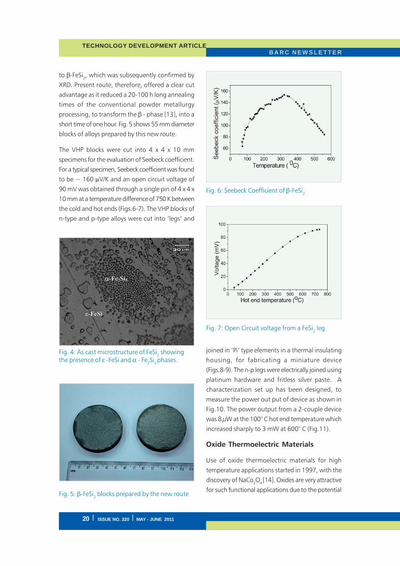
specimens for the evaluation of Seebeck coefficient.
For a typical specimen, Seebeck coefficient was found
to be ~ 160 μV/K and an open circuit voltage of
90 mV was obtained through a single pin of 4 x 4 x
10 mm at a temperature difference of 750 K between
the cold and hot ends (Figs.6-7). The VHP blocks of
n-type and p-type alloys were cut into ‘legs’ and
joined in ‘Pi’ type elements in a thermal insulating
housing, for fabricating a miniature device
(Figs.8-9). The n-p legs were electrically joined using
platinum hardware and fritless silver paste. A
characterization set up has been designed, to
measure the power out put of device as shown in
Fig.10. The power output from a 2-couple device
was 8 μW at the 100° C hot end temperature which
increased sharply to 3 mW at 600° C (Fig.11).
Oxide Thermoelectric Materials
Use of oxide thermoelectric materials for high
temperature applications started in 1997, with the
discovery of NaCo2O
4 [14]. Oxides are very attractive
for such functional applications due to the potential
Fig. 7: Open Circuit voltage from a FeSi2 leg
Fig. 6: Seebeck Coefficient of β-FeSi2
Fig. 5: β-FeSi2 blocks prepared by the new route
Fig. 4: As cast microstructure of FeSi2 showing
the presence of ε -FeSi and α - Fe2Si
5
phases.

ISSUE NO. 320 I MAY - JUNE 2011 I 21
B A R C N E W S L E T T E RTECHNOLOGY DEVELOPMENT ARTICLE
maneuverability of their properties with doping
different cations. Till date, various oxide materials
have been discovered for such applications e.g.
Ca3Co
4O
9, BaPbO
3, CaMnO
3, NiO, ZnO etc. In the
present work, results on Gd doped Ca3Co
4O
9 (termed
as 349-phase) and La doped CaMnO
3 are presented.
Both these materials were synthesized in bulk by
the controlled combustion synthesis route. In this
processing route, thermal dehydration of aqueous
solutions containing metal nitrates and a
carbonaceous ‘fuel’ gives rise to a viscous gel which
on further heating undergoes auto-combustion.
Subsequent calcination of auto-combusted
precursors may be required, to obtain desired oxide
powders. Citric acid and manganese acetate have
been used as fuel, for the synthesis of p–type
Ca2.75
Gd0.25
Co4O
9 and n–type Ca
0.92La
0.08MnO
3,
respectively. Ultra-fine powders (average particle size
<1 μm) were obtained after calcination at 800 °C.
These powders were subsequently consolidated.
Ca0.92
La0.08
MnO3
powders were compacted and
sintered at 1250 °C in air to nearly full density
(Fig.12). On the other hand, Ca2.75
Gd0.25
Co4O
9
powders could not be heated to temperatures higher
than 950 °C, because the 349-phase is known to
decompose into 326-phase according to the
following reaction:
Ca3Co
4O
9 → Ca
3Co
2O
6 + Co
2O
3
Fig. 8: β-FeSi2 thermo-elements
Fig. 9: Housing for thermoelectric device
Fig. 10: Measurement set-up for thermoelectricdevice
Fig. 11: Power output of FeSi2 TE device properties

22 I ISSUE NO. 320 I MAY - JUNE 2011
B A R C N E W S L E T T E RTECHNOLOGY DEVELOPMENT ARTICLE
Therefore, Ca2.75
Gd0.25
Co4O
9 (CGCO) powders were
vacuum hot pressed at 900 °C to nearly dense pellets
(Fig.13).
The dense compacts of n–type as well as p–type
ceramics were cut into pins of dimensions 4 mm x
3 mm x 8 mm for measurement of properties and
subsequent integration into miniature devices. The
fabricated n-type pin of Ca0.92
La0.08
MnO3 (CLMO)
has shown the Seebeck coefficient and electrical
conductivity of about 110 μVK-1 and 100 Scm-1
whereas the p-type pin of Ca2.75
Gd0.25
Co4O
9 exhibited
the Seebeck coefficient and electrical conductivity
of 140 μVK-1 and about 85 Scm-1 at 800°C,
respectively. These functional properties obtained
for both the ceramics indicated their suitability for
high temperature thermo-electric devices. For
making electrical contacts, each leg was coated with
Pt-paste and subsequently these legs were electrically
joined by a platinum mesh. A two-couple device
was integrated using the above n-type and p-type
pins as shown in Fig.14. The device showed a power
output of 18 mW at the hot end temperature of
750 °C (Fig.15).
Fig. 12: Micrograph of Ca0.92
La0.08
MnO3 sintered
at 1250 °C in air
Fig. 13: Fracture surface of Ca2.75
Gd0.25
Co4O
9
vacuum hot pressed at 900 °C
Fig. 15: Power output of oxide TE device
Fig. 14: Miniature oxide thermoelectric device

ISSUE NO. 320 I MAY - JUNE 2011 I 23
B A R C N E W S L E T T E RTECHNOLOGY DEVELOPMENT ARTICLE
Development of electrical contacts with
improved electrical, mechanical and
thermal properties
For high temperature applications, contact material
has to be metallurgically bonded to get significant
lower contact resistance [15,16]. Silver based
materials (including its alloys and composites) and
platinum are the most popular contact materials for
the oxide based high temperature thermoelectric
devices.
A silver based composite, which is stable in air up
to about 930 °C, has been used, for the
development of efficient electrical contact. Tapes
of the contact material with typical thickness of
50-100 μm have been prepared, using organic-
based slurry through the Doctor-blade tape casting
technique. These tapes were placed over faces of
thermo-electric powder columns and were hot
pressed along with thermo-electric materials using
a multi-cavity die. The quality of metallurgical
bonding of the hot-pressed thermo-elements, was
tested for the adherence test, which showed that
the bond strength of the contact was higher than 6
MPa. Such a high strength is indicative of a good
quality metallurgical bonding of the contact with
thermo-elements. The hot-pressed thermo-elements
with the silver-based metallization were subjected
to resistivity measurements as a function of
temperature. The contact produced by the present
technique showed, that in the temperature range
700-800°C, the resistance contribution of the contact
was about 17-18% of the total internal resistance,
against the conventional value of 40-50%.
Therefore, the process has been further taken up
for the fabrication of multi-elements for multi-
component devices. Fig. 17 shows a photograph
of hot-pressed mutli-elements with contacts.
Related issues for performance
enhancement
Performance of a thermoelectric device can be
improved by two ways: by increasing the figure of
merit Z, which calls for improving material properties
like electrical conductivity, thermal conductivity and
Seebeck coefficient, and/or by increasing the
packaging density of the device.
Thermoelectric properties of FeSi2 based materials
may be further enhanced, by dispersing fine oxide
particles in the matrix. Initial experiments on this
study have given encouraging results. Another
relevant area of the study is the transformation of
any residual α or ε phases in the VHP blocks into
β phase using post-VHP annealing treatment.
In the case of oxide TE ceramics, doping of rare–
earth elements are expected to change the functional
Fig. 16: SEM micrograph showing metallurgicallybonded thermoelectic material with the contactmaterial developed using hot press technique.
Fig. 17: Photograph showing hot pressed thermo-elements with contacts

24 I ISSUE NO. 320 I MAY - JUNE 2011
B A R C N E W S L E T T E RTECHNOLOGY DEVELOPMENT ARTICLE
properties. It is, therefore, interesting to change the
stoichiometry of TE oxides systemically and study
its effect on the transformation temperature as each
rare–earth element has its own specific charge ratio,
thus stabilizing the 349 phase. Further work is being
continued, for making multi-elemental devices for
higher power output. The research work on the
development of better electrical contacts with
improved thermal and electrical characteristics for
lowering parasitic resistances and increased power,
is of utmost importance. In this context, a novel
conceptual design of monolithic multi-element
device has been proposed, and a dummy device
using surrogate material has been fabricated.
Summary
Thermoelectric materials based on intermetallic FeSi2
as well as oxide ceramics were developed for high
temperature applications. For β-FeSi2 based alloys,
such as n-type Fe0.94
Co0.06
Si2 and ρ-type
Fe0.91
Mn0.09
Si2,
a new synthesis route involving a
combination of arc-melting and VHP produced the
material of same quality within hour against
conventional time of production of 100 hours. The
elements were cut from the VHP blocks of the
synthesized material and a two-couple miniature
device was fabricated. The device exhibited 3 mW
power at 600 °C. The oxide ceramic materials n–
type Ca0.92
La0.08
MnO3 and p–type Ca
2.75Gd
0.25Co
4O
9
were synthesized by combustion technique. These
were consolidated into dense pellets by air sintering
and VHP, respectively. A miniature device has been
fabricated from the elements cut from consolidated
pellets. The device showed power output of 18 mW
at 750 °C. In addition, improvised electrical contacts
were prepared using silver composite which lowered
the internal resistance of the device to one third of
the conventional values.
Acknowledgements
Authors are thankful to Dr. K. Bhanumurthy, Head,
SIRD, Dr. Madangopal Krishnan, Head, Functional
Materials Section, MSD, Dr. G. K. Dey, Head, MSD
and Dr. S. C. Gupta, Head, TPD for fruitful
suggestions and for providing facilities. We are
grateful to Dr. A. K. Suri, Director, Materials Group
for his keen interest, constant encouragement and
support.
References
1. K.H.J. Buschow, R. W. Cahn, M.C.
Flemmings, B. Ilschner, E.J. Kramer, S.
Mahajan (eds.), Enclyclopedia of Materials
Science and Technology, vol. 10, Elsevier,
(2001).
2. D.M. Rowe (ed.), CRC Handbook of
Thermoelectrics, CRC press, London, (1995).
3. K. Nogi, T. Kita, X.-Q. Yan, Mater. Sci. &
Engg., A307, 129-133, (2001).
4. M. Kubo, M. Shinoda, T. Furuhata, K.
Kitagawa, Energy, 30, 2156-2170, (2005).
5. Deep Prakash, M. Syambabu, C. Gayner, R.
Tewari and P.K. Sinha, PM-11, International
Conference on Powder Metallurgy, February
3-5, Pune, India (2011).
6. W. Shin, N. Murayama, K. Ikeda and S. Sago,
Jpn. J. Appl. Phys., Part 1, 39, 1254, (2000).
7. I. Matsubara, R. Funahashi, T. Takeuchi, S.
Sodeoka, T. Shimizu and K. Ueno, Appl. Phys.
Lett., 78, 3627, (2001).
8. Oxide TE – J. G. Noudem, S. Lemonnier, M.
Pravel, E. S. Reddy, E. Guilmeau and C.
Goupil, Key Engg. Mater., 352, 245-250,
(2007).
9. G. H. Rinehart, Prog. Nucl. Energy, 39, 305-
319, (2001).
10. H. Nagai, K.-I. Nagai, T. Katsura, S.
Katsuyama, K. Majima and M. Ito, Mater.
Trans. JIM, 39, 1140-45, (1998).

ISSUE NO. 320 I MAY - JUNE 2011 I 25
B A R C N E W S L E T T E RTECHNOLOGY DEVELOPMENT ARTICLE
11. A. Sugiyama, K. Kobayashi, A. Matsumoto,
K. Ozaki and T. Nishio, J. Jap. Inst. Met., 63,
1145-48, (1999).
12. W.-S. Cho and K. Park, J. Mater. Sci: Mater.
Elec., 11, 319-24, (2000).
13. W.-S. Cho, S.-W. Choi and K. Park, Mater.
Sci. & Engg., B68, 116-22, (1999).
14. I. Terasaki, Y. Sasago and K.Uchinokura :
Phys. Rev. B 56, R12685, (1997).
15. T. Caillat, J.- P. Fleurial, G. J. Snyder, A. Zoltan,
D. Zoltan, and A. Borshchevsky, A New High
Efficiency Segmented Thermoelectric
Unicouple, 34 th Intersociety Energy
Conversion Engineering Conference p. 2567
(1999).
16. R. Funahashi, S. Urata, K. Mizuno, T. Kouuchi
and M. Mikami, Appl. Phys. Lett. 85 1036
(2004).
Forthcoming Meeting
DAE – BRNS Theme Meeting on
Emerging Trends in Applications
of Lasers & Accelerators in
Nanomaterials
(ETALAN-2011)
ETALAN-2011 will be held on20 – 21 October, 2011, at theMultipurpose Hall, Training SchoolHostel, BARC, Anushaktinagar, Mumbai.It is being organized by the Radiation &Photochemistry Division, BARC and theIndian Society for Radiation andPhotochemical Sciences (ISRAPS).
The theme meeting aims at discussingthe current status and future challengesin the following areas:
• Synthesis & Characterizationof nanomaterials using lasers& accelerators
• Modification/tuning of propertiesof nanomaterials using lasers& accelerators
• Fast & Ultra fast Spectroscopy on andwith nanomaterials using lasers& accelerators
• Use of nanomaterials in lasers& accelerators.
Scientific sessions will include invitedtalks by experts as well as youngresearchers across the country and posterpresentations of contributory papers.
All correspondence should be addressedto:
Secretary, ETALAN-2011Radiation & Photochemistry DivisionBhabha Atomic Research Centre,Trombay, Mumbai 400 085E mail: [email protected]: 91-22-25590297, 25590309FAX: 91-22-25505331

26 I ISSUE NO. 320 I MAY - JUNE 2011
B A R C N E W S L E T T E RTECHNOLOGY DEVELOPMENT ARTICLE
Development and Fabrication of Superconducting
Hybrid Cable-In-Conduit-Conductor (CICC) for
Indigenous Fusion Programme
A.K. Singh, M.M. Hussain, K.K. Abdulla and R.P. Singh
Atomic Fuels Division
Abstract
The Atomic Fuels Division has initiated development and fabrication of CICC of various configurations, for
superconducting fusion grade magnets required for our indigenous Fusion Programme. The process involves
development of high grade superconducting multifilamentary wire, multi stage cabling of superconducting
as well as copper wires and, finally, jacketing of the cables in SS316LN tubes. The overview of the development
and fabrication of CICC is presented in this article.
Introduction
Thermo-nuclear fusion plasmas are magnetically
confined in devices known as Tokamaks. The
magnetic confinement is attained by steady or time
varying magnetic fields, produced by large high
current carrying superconducting magnets. These
robust superconducting magnets are usually
constructed of cables of NbTi, Nb3Sn & Nb
3Al
superconductor composites incorporated within
cable-in-conduit-conductor (CICC) configurations.
The most important requirement is that the
superconducting CICC be stable in the operating
reactor plasma environment. CICC constitutes more
than one sixth of the cost of a fusion reactor.
The Institute for Plasma Research and the Atomic
Fuels Division, BARC have launched a joint initiative
towards an indigenous development of fusion grade
superconductors and cables. This effort is ultimately
aimed at generating a complete technology and
process know-how, for making fusion grade
superconductors and cables and using these for
developing prototype of large size, high field, high
current carrying magnets.
Fabrication Technology
The fabrication technology of superconducting CICC
consists of the following stages:
a) Superconducting wire fabrication
b) Cabling and wrapping
c) Insertion and Jacketing.
a) Superconducting wire fabrication
The most critical component of a CICC is the
multifilamentary superconducting wire, that is
capable of carrying very high currents required for
the generation of intense magnetic fields. Niobium-
Titanium and Nb3Sn superconducting composites
have quite a long history in the era of applied
superconductivity. Virtually, all of the large
superconducting magnet systems that have been
constructed so far, have used Nb-Ti or Nb3Sn
superconductors. The Nb-Ti alloys are ductile and
can be co-processed with copper into a wide range
of composite conductors. On the other hand, Nb3Sn
is a brittle inter-metallic compound and is created
by heat treatments carried out at the end of the

ISSUE NO. 320 I MAY - JUNE 2011 I 27
B A R C N E W S L E T T E RTECHNOLOGY DEVELOPMENT ARTICLE
fabrication cycle. While the Nb3Sn based CICC is
used for high field application (~12 Tesla), the Nb-
Ti based CICC is only suitable for low field
application. The fabrication of Nb-Ti based fusion
grade CICC is discussed in this paper.
The parameters important in the design of a
superconductor are [1]:
a) Critical temperature Tc-
b) Critical magnetic field Hc
c) Critical current density Jc .
Both Tc-
& H
c are dependent only on the chemical
composition of the alloy, whereas the critical current
density Jc, is a structure dependent property and is
strongly affected by the density, size and distribution
of imperfections such as, dislocations, grain
boundaries and precipitates, which can act as flux
pinning centers [3].
The fabrication parameters are crucial to achieving
a suitable microstructure in the composite
conductors and the required electrical and
mechanical properties. The underlying composite
material fabrication technology needs to be fine-
tuned to meet a range of disparate demands such
as, adequate mechanical strength or the right
combination of superconducting and normal
conducting properties, for obtaining stabilization.
The steps involved in the fabrication of
superconducting wire are:
1. Preparation of hexagonal elements
2. Assembly of these elements in OFHC copper
sleeve to form extrusion billet
3. EB welding of the billet assembly
4. Hot Extrusion
5. Cold drawing with intermediate vacuum ageing
treatment and
6. Twisting.
Based on an extensive development work carried
out, which included composite billet design,
optimisation of parameters for extrusion, drawing
and ageing treatment to obtain suitable shape, size
and distribution of α -Ti precipitates for flux pinning
centres, an appropriate fabrication route has been
standardised for 0.80 mm dia. wire containing ~500
Nb-Ti filaments, each of 25 micron size, with Cu:SC
(matrix to superconducting element) ratio of 1.15:1.
Single length wires of 10 Km have been successfully
produced [3,4], which show a maximum critical
current of 1500 Amps (measured in short samples
in 5.5 Tesla field and 4.2 K). Fig. 1 shows the typical
cross section a 0.80mm dia SC wire. Fig. 2 shows
the normal to superconducting second order phase
transformation at ~9.8K, while Fig. 3 shows the
Fig. 1: Cross-section of 0.8 mm strand showingNb-Ti filaments
Fig. 2: The second order normal to superconductingphase transition under 0 T and 5 T fields

28 I ISSUE NO. 320 I MAY - JUNE 2011
B A R C N E W S L E T T E RTECHNOLOGY DEVELOPMENT ARTICLE
resistance drop with temperature in absence and
presence of a 5 Tesla field (these results are for a
0.80mm dia wire).
b) Cabling Technology
The problem of stability is an important criterion for
the design of all practical superconducting wire
magnets [2]. On account of the resistance in the
normal state being very high and also the current
density employed in these magnets being high, a
local transition from superconducting to normal
state causes intense local heating. With the heat
spreading to neighbouring regions of the winding,
the normal zone spreads rapidly till a point, when
all stored energy is dissipated as heat. Compared to
other types of superconducting magnets, the
superconducting wire ones are susceptible to this
‘degradation’ or ‘quenching’ phenomenon at much
lower currents. However, degradation is ameliorated
by making a composite conductor in which the
superconductor wire is in intimate contact with a
good thermal conductor such as OFHC copper: local
cooling is provided to each conductor in winding.
Additionally, the cabling is designed to provide
sufficient voids for flow of super fluid Helium
through the CICC.
The cabling of a CICC involves several stages of
twisting that are dictated by the physical application
and the engineering aspects. These details were first
thoroughly investigated and followed by several
hardware trials with available infrastructure and
machineries to develop an optimized design of the
CICC. The schematic of the optimized twisting
pattern is shown in Fig.4. The cable obtained after
stage 4 is shown in Fig.5.
c) Jacketing Technology
We have developed an indigenous swaging method
for jacketing the cable. Here, the final stage cable is
wrapped in a half-overlap pattern with SS304L tape
and inserted into a round SS316LN tube of suitable
size. This is further compacted and shaped into a
square cross section by swaging. The finished CICC
is wound onto a 2m dia. barrel spool using a bender.
Fig. 3: Resistance Drop with temperature under 0 Tand 5 T fields
Fig. 4: Schematic of the multi stage cabling pattern
Fig. 5: Final Stage Cable Containing 504 wires of0.8 mm dia

ISSUE NO. 320 I MAY - JUNE 2011 I 29
B A R C N E W S L E T T E RTECHNOLOGY DEVELOPMENT ARTICLE
Figs. 6 and 7 show the duplex swaging machine
utilised for jacketing and the square cross section
swaging die, respectively. The pulling force is a
critical parameter in this method and determines
the void fraction of the CICC. This technique has
specific advantages over the conventional technique
in which the jacketing is done by longitudinal seam
welding of a strip cold rolled onto the cabled
conductor [2].
The latter technique requires careful automated
welding to avoid heating of the cabled strands (the
conventional technique has been used in the CICC
of Steady State Tokamak (SST) -1 coming up at IPR,
Gandhinagar).
A 60m long 30kA hybrid CICC of 30mm x30mm
square cross section has been fabricated by the
Fig. 6: Duplex Swaging machine at AFD, BARC
Fig. 7: Swaging Die developed at AFD, BARC
Fig. 8: Foil wrapping on final stage cable
Fig. 9: Insertion of wrapped cable in circular tube
Fig. 10: Swaging of SS316LN tube containing cableto Square cross section CICC

30 I ISSUE NO. 320 I MAY - JUNE 2011
B A R C N E W S L E T T E RTECHNOLOGY DEVELOPMENT ARTICLE
indigenous technique. Figs. 8 -13 show some of
the important stages of fabrication.
The CICC developed at BARC has shown a current
carrying capacity of 11000 A at 6 K, against the
designed value of 10000 A at 4.5 K supercritical
helium. Apart from this, the hybrid conductor has
about 25% less superconductor compared to that
used in SST-I.
Future Work
An on-line fabrication facility is being set up using
several shop floor innovations that will facilitate the
fabrication of CICC in a comparatively smaller space.
The facility consists of foil wrapping setup, a
triangular mechanised cable insertion system, orbital
welding machine along with tube handling system,
a set of swaging, bending and coil winding
machines. Several trials have already been carried
out for the insertion of final stage wrapped cable
made of copper wire in SS tube, the orbital welding
of these tubes containing cable, the round to round
as well as round to square swaging and bending
with coil winding. Further optimisation of the
process is in progress.
References
1. P. J. Lee and D. C. Larbalestier, “Development
of nanometer scale structures in composites of
Nb-Ti and their effect on the superconducting
critical current density” Acta Metall., Vol. 35
(No. 10), 1987, p 2523-2536.
2. F. Hosono, G. Iwaki, S. Inaba, T. Suzuku,
K. Hiroshima, K. Kikuchi, K. Chida, M. Watahiki,
K. Kamata, Subrata Pradhan and Y. C. Saxena,
“Production of Nb-Ti CICC’s for SST-1 project
at IPR” IEEE Trans. On Applied
Superconductivity, Vol. 11, No. 1, March 2001
p 2014-2017.
3. A. K. Singh, M. M. Hussain, S. P. Singh and
V. G. Date, “Low Temperature Superconductor
– Fabrication and Application.” ATM, IIM,
Vadodara, Nov. 14-17, 2002 & News Letter,
IIM Mumbai Chapter, p 12-18, Dec., 2002.
4. A. K. Singh, M. M. Hussain, S. P. Singh and
R. P. Singh “Fabrication of multifilamentary
Nb-Ti superconducting wire and cable:
technological capabilities available at Atomic
Fuels Division, BARC” BARC Newsletter, May
2004, No. 244, p 11-14.
Fig. 11: Bending of CICC
Fig. 12: CICC in 2m dia coil form
Fig. 13: Cross section of CICC

ISSUE NO. 320 I MAY - JUNE 2011 I 31
B A R C N E W S L E T T E RFEATURE ARTICLE
Multi-Detector Environmental Radiation Monitor
with Multichannel Data Communication for
Indian Environmental Radiation MOnitoring
Network (IERMON)
M.D. Patel, M.P. Ratheesh, M.S. Prakasha, S.S. Salunkhe,
A. Vinod Kumar, V.D. Puranik and C.K.G. Nair (Retd.)
Environmental Assessment Division
Abstract
A solar powered system for online monitoring of environmental radiation with multiple detectors has been
designed, developed and produced. Multiple GM tube detectors have been used to extend the range of
measurement from 50 nano Gy/hr to 20 Gy/hr and to enhance the reliability of the system. Online data
communication using GSM based and direct LAN based communication has been incorporated. Options
for use of power supply from mains powered and battery powered have been enabled. Care has been taken
to make it weather-proof, compact, elegant and reliable. The development is a part of the ongoing program
of country-wide deployment of radiation monitors under “Indian Environmental Radiation MOnitoring
Network (IERMON).
Introduction
Fears about nuclear radiation and its effects are often
raised in the media and in the general public. The
success of establishment of large scale nuclear power
programme envisaged by our country, also depends
on the public perception about nuclear radiation.
Adequate number of online and realtime radiation
monitoring systems along with availability of the
information in the public domain, will inform the
public about the omnipresent environmental
radiation due to natural sources and its geographical
variation. Display of marginal or insignificant
change in the radiation levels due to establishment
of nuclear power plant as compared to natural
background radiation will eliminate the false
propaganda of increase in radiation levels in the
public domain. In addition, a countrywide network
of environmental radiation monitor serves as an early
warning system for detection and for activating
emergency response in case of an unlikely event of
nuclear emergency either in our own country or in
the neighbouring countries.
Ionizing radiation has always been a part of the
human environment due to cosmic rays and due to
the natural radioactive elements present in the earth’s
crust. The natural radiation is of: a) Terrestrial origin
b) Cosmic origin. The terrestrial radiation is due to
the presence of naturally occurring radioactive
substances like Uranium, Thorium and Potassium
isotope (K-40) in earth’s crust. Cosmic radiation
comes through the earth’s atmosphere, from the
sun and galaxies. This increases with latitude &
altitude. It is more at poles than at equator.
It is essential that a system which is meant for
detection of nuclear emergency must be installed
in open environment so that the changes in
environmental radiation level can be readily and
accurately monitored. The traditional systems work
on mains power which is subject to various problems

32 I ISSUE NO. 320 I MAY - JUNE 2011
B A R C N E W S L E T T E RFEATURE ARTICLE
like load shedding, power fluctuations, power
transients etc. Also it is inconvenient to provide
mains power when the system is required to be
installed in the field in remote areas. It is found that
provision of battery backup is not sufficient in the
cases involving extended or frequent power
shutdown. Hence, it is desirable that the
environmental monitor is powered by other sources
of power such as solar panels, wind turbines, etc.
with battery backup.
Data communication is another requirement for
effective monitoring. The radiation incident should
be reported with minimum possible time lag. Hence,
the system should have redundant communication
channel. Presently the technologies available for data
communication from field systems are (1) land line
telephone (dialup and leased line), (2) mobile phone
network (GSM and CDMA), (3) VSAT, (4) RF, etc.
Indian Environmental Radiation Monitoring Network
(IERMON) is a countrywide network of online
monitoring stations located at various parts of the
country and with central monitoring station located
in Mumbai. The network is designed, developed,
established and managed by the Environmental
Assessment Division of Bhabha Atomic Research
Centre, Mumbai. The network employs systems
developed indigenously, keeping in mind the general
and strategic requirements of the country, also
geographical condition and available resources for
power and communication.
The new IERMON System
The new IERMON system employs multiple radiation
detectors for redundancy and extended range of
measurement. The system has multichannel data
communication facility. The system works on solar
power with battery backup. It is designed with the
following capabilities:
• Zero Down Time: The system is ensured to
work reliably at any point of time. Adequate
redundancy has been provided in measurement
and data communication. All components are
of MIL grade, wherever possible.
• Low Maintenance: The requirement of visiting
the site for preventive maintenance and/or
calibration check is not more than once in
an year.
• Easy Maintenance: It is easy for a trained
layman to carry out the maintenance.
• Outdoor Installation: The system is designed
for outdoor installation for measurement of
natural background radiation as well as
enhanced radiation levels due to accidental
release of radioactivity into the atmosphere.
• Energy Harvesting: The system uses a natural
power source like solar power pack for its
working.
• Ease of Communication: Low cost and easy
availability are the main criteria for selecting
mode of data communication. The system in
addition, has wired communication for local
display and redundancy.
• Weather proof: The system operates at
ambient air temperature between -20ºC and
+60ºC and ambient relative humidity up to
100%.
The technical specification of the system developed
are :
1. Environmental and Fallout Dose
Measurements
Detected radiation : Gamma radiation
Detectors : Energy compensated
GM tubes
Energy response : 35 keV to 2 MeV
(combined)
Measurement range : 50 nanoGy/h to 20 Gy/h
(combined)
(Gy = Gray, keV = kilo electron Volt, MeV = Mega
electron Volt)
2. Environmental
Operating temperature : -20ºC to +60ºC
Relative humidity : up to 100%

ISSUE NO. 320 I MAY - JUNE 2011 I 33
B A R C N E W S L E T T E RFEATURE ARTICLE
Fig. 1: Block diagram of the IERMON system
System enclosure : IP68 compliance for
detectors & Electronics
Housing.
IP66 for battery housing
with support for solar
panel.
EMI/EMC : IEC applicable standards.
3. Power Supply
• Solar panel, 20W, 9V
• Sealed Maintenance Free Battery, 6V/24Ah
4. System Description
The following types of radiation detectors are used
in the system:
• High sensitivity GM counters (GM1 and
GM2 in Fig. 1)
• Low sensitivity GM counter (GM3
in Fig. 1)
The high voltage (HV) required for GM1 and GM2
is 450V and for GM3 it is 550V. Separate HV module
is implemented for GM1 and GM2, though both
the tubes can be operated from a single supply.
Using separate HV module enhances redundancy
but it leads to increased power consumption.
Selection of HV module is critical for this reason.
To reduce the power consumption only one way
transmission i.e. from system to central station is
activated, though the system is capable of two way
communication. The LAN Socket Modem shown
in the block diagram (Fig. 1) is for LAN based
communication. Fiber-based communication and
satellite-based data communication can be added
with little modification, if such facility is available
at local station. This port is also used by service
engineer for interfacing with computer at the time
of system maintenance/calibration.

34 I ISSUE NO. 320 I MAY - JUNE 2011
B A R C N E W S L E T T E RFEATURE ARTICLE
Fig.2 PCB showing detector locations in IERMONSystem (PCB Size : 8.5cm x 45cm)Fig.3 Photograph of complete IERMON System(Height : 90cm; Base Plate : 30cm x 30cm ;Weight : 25kg)
Fig. 2 Fig. 3
The Solar Power Pack consists of solar panel, charge
control relay and SMF (Sealed Maintenance Free)
battery. The present system is designed to operate
using 20W solar panel with 6V/24Ah battery. The
system can work for 15 days in a cloudy weather
condition using only the supply from the back up
battery. Transient Suppression Devices are used to
protect the system from electrical transients that
may enter the system through the cable from solar
panel.
The pulses from the GM counters are converted to
transistor transistor logic (TTL) pulses using Pulse
Shaper circuits. The TTL pulses from the Pulse Shaper
are fed to the inputs of the counters of the micro
controller.
The micro controller is programmed to read the
counter values at every five minutes without
disturbing the counter. The extrapolated hourly dose
is computed from the counts and checked with the
preset trigger level for verifying any abnormal
increase of radiation. If at least two out of the three
detectors agree on exceeding a cretain trigger
level, an ‘event flag’ is set and the processor
transmits the dose level every five minutes until the
dose level falls below the trigger level. Normal
averaging time is one hour and is synchronized with
the Real Time Clock (RTC). At the end of the counting
period (signalled by the ‘end-of-hour’ interrupt from
RTC), the counts are converted to dose rate using
appropriate conversion factor derived from the
calibration lookup table. Necessary correction is
applied if the counting time is less than one hour,
as normally the case when the system is started or
restarted. The hourly dose is stored in memory. A
photograph of the printed circuit board (PCB) of
the system and the complete system is shown in
Fig. 2 and Fig. 3.
The system performance has been tested in the field
for about 6 months. The system has performed
uninterrupted, unattended as per the technical
requirement in the field conditions.
Applications of the new IERMON System
The new IERMON System was designed for
deployment in the countrywide Indian
Environmental Radiation Monitoring Network
(IERMON). More than 100 such systems have been
deployed all over India and it is targeted to achieve
installation of 500 units in a span of 2 years. The
system can also be used for other applications
involving measurement of environmental gamma
radiation. In cases where operation using mains
power is required, the system can accommodate
an SMPS board. The system can also be used only
with built-in battery and with this, the system can
work for six months in data logging mode without
communication. For in-plant monitoring, where the
system is powered by mains, power data
communication can be also achieved through the
existing telephone lines.
Acknowledgements
The authors are indebted to Director, Health Safety
& Environment Group and Associate Director, Health
Safety & Environment Group, BARC for their
constant support and inspiration. This work would
not have been successful without the active
participation of the members of the divisional
workshop and other colleagues in the Environmental
Systems and Networking Section of the division.

ISSUE NO. 320 I MAY - JUNE 2011 I 35
B A R C N E W S L E T T E RFEATURE ARTICLE
Abstract
The article discusses the importance of Polarized Neutron Reflectometry (PNR) in understanding magneticstructure of thin films. A PNR has been installed in the guide tube laboratory of Dhruva reactor. Thisinstrument has been used successfully, to understand magnetic structure in thin films. Some of the resultsobtained on magnetic non-magnetic multilayer samples have been presented, to demonstrate how PNRhas been successful in characterizing interface magnetic structure.
Mapping Interfaces in Magnetic Thin Films with
Neutron Reflectometry
Saibal Basu and Surendra Singh
Solid State Physics Division
Introduction
Polarized neutron reflectometry is one of the most
important non-destructive tools, in understanding
and characterizing interfaces in various thin films of
interest. Historically Fermi and Zinn were the first
to report in the pages of Physical Review journal in
1946, neutron reflectivity measurement for finding
out coherent nuclear scattering cross-section of
various materials [1]. Approximately a decade later
the first report on x-ray reflectivity for thin film
characterization from L. G. Parratt appeared [2]. The
reincarnation of neutron reflectometry as a useful
tool for studying thin films and interface magnetic
structure is due to G. P. Felcher of Argonne National
Laboratory in 1980s. Later, his comments in a
popular article written in Neutron News is worth
mentioning [3]:
“Ten years ago at a modest spallation-neutron source
at Argonne National Laboratory, a “gizmo” was
installed which was later christened as a
reflectometer. The popularity of the gizmo spread
like wild fire: now virtually all neutron sources
possess at least one of them. Some are graced by
splendid names: CRISP and SURF at Rutherford,
TOREMA at Jülich, DESIR in Saclay and EVA in
Grenoble.”
It is the rich information content with resolution in
nanometer length scale regarding physical and
magnetic structures of thin films, that has made
Polarized Neutron Reflectometry (PNR) such an
important and popular tool. The popularity of
neutron reflectometry is well augmented by that of
X-ray Reflectometry (XRR). Both use the phenomena
of reflection of waves from thin film surfaces. Since
the x-rays interact with the atomic electron cloud
and the neutrons with the nuclei, the refractive
index for x-rays depends on the electron density of
the material and the refractive index for neutrons
depend on the coherent scattering length
density for neutron-nuclear interaction in the
material. This basic difference makes them
complementary techniques for study of surfaces and
interfaces in thin films. In addition, the neutron
possesses a magnetic moment of -1.91 μN (nuclear
magneton) and PNR is ideally suited for
understanding magnetic structure of multilayer
samples. PNR has gained importance also because
of rapidly growing interest in thin film multilayers
of magnetic and non-magnetic materials, giving rise
to various important effects like Giant Magneto-
Resistance and Spin-Valve effects. These are artificial

36 I ISSUE NO. 320 I MAY - JUNE 2011
B A R C N E W S L E T T E RFEATURE ARTICLE
materials that are important, fundamentally as well
as technologically. Spin Valve based DRAM memory
devices have already appeared in the market. It is
important to characterize these materials at
nanometer length scale, to correlate their property-
structure relationship. In recent years PNR has come
handy in such studies. Another important property
of neutrons is its capability to distinguish between
the isotopes: hydrogen and deuterium, because the
coherent scattering lengths are quite different for
these two isotopes. This makes neutron an ideal
tool to study liquid air or liquid/liquid interfaces and
organic films. Presently neutron reflectometry
technique is considered so important, that the
Rutherford Appleton Laboratory, U. K. in their
recently installed second target station at ISIS
spallation neutron source, has installed a so-called
neutron reflectometer “village” consisting of three
neutron reflectometers: one designed for horizontal
sample geometry targeting liquid-air interfaces, one
for vertical sample geometry for studying magnetic
interfaces and another one for studying off-specular
or diffuse reflectivity from surfaces and interfaces.
A Polarized Neutron Reflectometer (PNR) has been
built in the Dhruva guide tube laboratory by the
Solid State Physics Division, BARC. This
reflectometer is being used routinely to study
magnetic structure in multilayer and thin films. We
will briefly discuss some of the results obtained from
this instrument on samples of interest.
Brief Exposition to Neutron
Reflectometry
A neutron at grazing incidence, experiences an
average potential in a medium, arising from neutron
–nucleus interaction:
( ) ( ) cohbRmhRV ρ
22π= (1)
potential translates to a refractive index ‘n’ for a
medium, given by
cohbn ρλπ2
12
−= (2)
Where λ is the wavelength of the neutron, This
simple expression tells us that depending on the
sign of ‘bcoh
’, the refractive index can be less than
or more than 1. For most materials ‘bcoh
’ is positive
and the refractive index is marginally less than 1: n
= 1- δ, where δ is typically about 10-5-10-6. Neutrons
are totally reflected up to a critical incident angle
θC’ given by:
πρλθ cohbc = (3)
For a good reflector like nickel, the value of
wavelength dependent critical angle θC is 6 arc
minutes / Å. For a medium in which the scattering
centres have magnetic moments, neutrons, because
of their inherent magnetic moment, will experience
a potential energy in a field ‘B(R)’, other than the
nuclear potential, given by:
( ) )R(BNRVmag ⋅−= μ (4)
If one considers that the film is so magnetized that
the magnetic moments are all aligned giving the
internal field ‘B(R)’, then the refractive index of the
medium for polarized neutrons is given by:
[ ]magcoh bb)R(mh)R(V ±= ρπ 22
(5)
We have defined a magnetic scattering length ‘bmag
’
arising out of ‘Vmag
’, where, the sign before the
magnetic scattering length depends on the neutron
magnetic moment parallel (+) or anti-parallel (-)
with respect to the polarization of the sample.
We will use the term up (+) and down (-) for these
two polarizations. Also, now the critical angles for
total external reflection for up (+) and down (-)
neutrons are different:
Where‘V(R)’ is the number density of the scattering
centres in the medium and ‘bcoh
(R)’ is the coherent
scattering length for each scattering centre. This

ISSUE NO. 320 I MAY - JUNE 2011 I 37
B A R C N E W S L E T T E RFEATURE ARTICLE
(6)
This shows that polarized neutron reflectometry from
magnetic samples will enable one to map the
magnetic field in a magnetic sample. Above the
critical angle, once the neutron beam starts
penetrating the medium, it gets reflected at every
interface due to refractive index contrast and the
reflected amplitudes interfere. The measured
reflectivity becomes structured. The oscillations in
reflectivity profile above the critical angle bear the
signature of layered structure of a thin film.
Fig. 1 shows simulated PNR profiles (R+ and R- ) for
a Fe-Cr multilayer thin film for up (+) and down
(-) neutrons. The reflectivity profile has been
plotted as a function of momentum transfer ‘Q’
[ ].
The scattering geometry has been shown in Fig. 2.
In specular reflectivity, angle of incidence (θi) and
angle of reflection (θf) are equal. We will show
data plotted either as functions of ‘Q’ the
momentum transfer or as functions of angle of
incidence.
The Fe-Cr film consists of ten periodic bilayers of
Fe-Cr with each bilayer approximately 10 nanometer
(nm) thick: total thickness being 100 nm. The
difference in the critical angles between ‘R+’ and ‘R-
‘ is due to the difference in potential seen by ‘+’
and ‘-‘ neutrons. The periodic repetition of the
bilayer gives rise to so-called “Bragg peaks” in the
reflected intensity, similar to the diffraction peaks
arising from atomic periodicity in crystal lattices.
The oscillations in intensity between two Bragg peaks
are due to the interference of neutron waves,
reflected from the top and bottom the film. These
are called “Kiessig oscillations” and are signatures
of total thickness of the film. The Bragg peaks are
absent in R- due to the fact, that for the down
neutrons there is a loss of contrast between Fe and
Cr layers [negative sign in potential, eqn. (5)] and
the periodic structure of the film is lost. This example
brings home the point, that the profiles R+ and R-
bear the signatures of physical and magnetic
structure of the Fe-Cr thin film.
Fig. 1: Spin-up (R+, red line) and spin-down (R-,blue line) reflectivity profile for an Fe/Cr multilayerthin film consisting of 10 bilayers of Fe and Cr. TheBragg peaks are due to periodicity of the bilayersand the Kiessig oscillations are signature of totalthickness of the film. The critical angle for R- is lowerthan R+ because refractive index for ‘+’ and ‘–‘neutrons are different
Fig. 2: The scattering geometry for neutronreflectometry. For specular reflectivity, angle ofincidence (θ
i) equals angle of reflection (θ
f) by Snell’s
law. For off-specular reflectivity this equality doesnot hold (blue rays). Roughness at the interface givesrise to off-specular reflectivity.

38 I ISSUE NO. 320 I MAY - JUNE 2011
B A R C N E W S L E T T E RFEATURE ARTICLE
Polarized Neutron Reflectometer in
Dhruva
The PNR instrument in Dhruva had been installed
on a curved neutron guide in Dhruva. Neutron guide
tubes transport neutrons using the phenomenon of
total external reflection from guide walls. The present
guide tubes at Dhruva, glass coated with Ni, were
fabricated and installed by the Solid State Physics
Division, to take neutron beams out from the reactor
hall to guide tube laboratory. Fig. 3(A) shows a
photograph of the reflectometer and schematic of
the same is shown in Fig. 3 (B) [4]. The reflectometer
has been designed for vertical sample geometry and
it can be used for specular as well as off-specular
(or diffuse) reflectometry (when angle of incidence
is not equal to angle of reflection). The neutron
beam coming from Dhruva reactor through the
curved guide is reflected by [113] planes of a Si
monochromator, to select a monochromatic beam
of 2.5 Å neutrons [neutron beams shown by red
arrows in Fig. 3 (A)]. These neutrons are collimated
to few arc minutes using a collimator made from
Cd slits. The collimated and monochromatic beam
of neutrons can be polarized using a polarizing super
mirror made from Co-Fe/Ti-Zr layers. This
monochromatic, highly-collimated and polarized
beam of neutrons is reflected from a vertical sample,
magnetized using a permanent magnet of 2K Gauss
strength and located at the centre of a rotation stage.
With the sample fixed at the centre, the sample
stage is rotated in steps (typically about 1 arc minute)
to collect the reflectivity pattern of the sample as a
function of angle of incidence ( θi ). Fig. 3 shows
the scattering geometry. In specular reflectivity,
angle of incidence ( θi ) and angle of reflection ( θ
f)
are equal. Since we use a PSD in this instrument,
we have the liberty to collect off-specular reflectivity
data also on this instrument [ fi θθ ≠ ]. Off-specular
reflectivity can reveal surface and interface
morphology. Presently we will discuss results of
specular reflectometry only.
Fig. 3: (A) Photograph of the polarized neutron reflectometer at Dhruva and (B) schematic of the same .‘M’ is the monochromator, S1 S2 S3’ are the cadmium slits for collimator, ‘SM’ is the super mirrorpolarizer, Sa’ is the sample stage with magnet, ‘An’ is the analyzer super mirror and ‘PSD’ is the
2He3
position sensitive neutron detector.

ISSUE NO. 320 I MAY - JUNE 2011 I 39
B A R C N E W S L E T T E RFEATURE ARTICLE
The rotation stage can rotate with a precision of
about 20 arc seconds and is capable of carrying
a load up to 400 Kg. It had been designed and
fabricated in the Centre for Design and Manufacture,
BARC specifically for the reflectometer. The reflected
beam is detected by a 30 cm long 2He3 neutron
Position Sensitive Detector (PSD), fabricated in the
solid state physics division. The PSD has a position
resolution of approximately 2 mm. The D. C. flipper
in the beam is used to flip the direction of neutron
spins for measuring reflectivity for spin-up (+) and
spin-down (-) neutrons. Due to intensity constraints
we do not use a spin analyzer for the reflected beam
at present, though the analyzer is available. In the
present set up, we are able to determine physical
and magnetic moment density as a function of
depth in the sample.
Some of the results are discussed here to demonstrate
the importance of polarized neutron reflectometry
in pinning interface structure of thin films.
Data Collection and Analysis
A stepper motor-based control system has been
designed for the high precision translation and
rotation stages. The monochromator is mounted
on a tilt and rotation stage assembly. The
spectrometer table can rotate around the
monochromator to facilitate θ –2θ coupling
between the monochromator and the table. This
allows changing the incident wavelength, if required.
The collimator is mounted on a high precision linear
stage, which can move the collimator in steps of
10 microns across the beam. The sample and the
magnet are mounted on a linear stage with one-
micron step size on top of the rotation stage. Sample
surface is brought to the centre of the rotation stage
with the help of this linear stage. The control system
for all the stepper motors is an integral unit with
the drivers and the power supplies located in it. It is
operated from the instrument’s PC through RS232
serial port communication.
Typical reflectivity data collected at a certain angle
of incidence θi looks like a Gaussian on the He3 PSD
channels [insets, Fig. 4]. The integrated counts under
the peaks, after background subtraction, give
intensity at particular angles as shown in Fig. 4.
Fig. 4: A typical neutron reflectivity profile as afunction of angle, collected on the PNR at Dhruva.The insets show intensity as a function of channelno. for a specific angle of incidence. Integratedintensity under each peak after backgroundsubtraction gives one data point in the reflectivityprofile
The analysis of PNR data requires getting the structure
of thin film sample in terms of layer thickness,
magnetic moment density, interface composition
and interface roughness from the experimental data
in ‘Q’ space. Ideally, it is through a Fourier inversion
from momentum space (‘Q’) one can get the
structure (magnetic or physical) in real space (‘R’).
In reality we can collect data only over a limited
momentum ‘Q’ or angular range and direct Fourier
transformation is not possible. We take recourse to
a ‘model-fitting’ where we start with an assumed
structure of the thin film sample and generate a
reflectivity pattern corresponding to this structure.
The initial model is modified through a χ2
minimization program, using some error
minimization software to modify the physical
parameters, so that we generate an intensity profile
matching the experimental data. We have developed
an optimization software using ‘Genetic Algorithm’.

40 I ISSUE NO. 320 I MAY - JUNE 2011
B A R C N E W S L E T T E RFEATURE ARTICLE
Samples Studied
a. Ni/Ti multilayer
Thin film multilayers of Ni/Ti have found
useful applications in the field of soft x-ray and
neutron optics, where they are used as highly
reflecting mirrors, supermirrors, polarizers and
monochromators etc. Further, TiNi alloy prepared
in thin film form, shows interesting shape memory
effect and this has been utilized to develop different
Micro-Electro Mechanical Systems (MEMS) such as
cantilevers, actuators etc. Bulk Ni/Ti alloys are also
important technological materials. We had prepared
Ni/Ti multilayers of various modulation lengths on
glass substrate by vacuum deposition. The sample
discussed here had ten Ni/Ti bilayers [Ni 5 nm and
Ti 7 nm] on glass substrate. The aim of the study
was to understand the growth of alloys at the
interfaces as a function of annealing [5]. The samples
were annealed first at 300 °C and then at 400°C for
a fixed time of 1.5 h. PNR was carried out on all
the samples before and after annealing. Fig. 5 shows
the PNR data from the sample before and after
annealing. The solid red circles are data for R+ and
the open blue circles are for θ -. Solid lines are fits
to the data. The drop in the intensity of the Bragg
peak and the gradual merging of the profiles for R+
and R- are due to mixing of Ni and Ti at the interfaces.
We had also carried out XRR on the same sample
(data not shown). Analyzing the XRR and PNR data,
we derived the physical and magnetic structure of
the sample. To highlight the complementary role of
XRR and PNR, we show the plots of physical density
as obtained from XRR from the sample before and
after annealing at 300 0C and 400 0C together with
the corresponding magnetic moment density profiles
in Figs. 6 (i) and 6 (ii) respectively. The physical
density of the as-deposited sample shows clear step-
like oscillations of density as a function of depth
[6(i) (a)] signifying periodic Ni and Ti layers of nearly
bulk density. The corresponding magnetic moment
density, obtained from PNR also shows the same
step-like nature as a function of depth. Ni is the
magnetic component in this sample and we found
an average magnetic moment of 0.4 μB (Bohr
magneton) per Ni atom in the Ni layers and a zero
magnetic moment density for the Ti layer from PNR
data. As we annealed the sample, alloying occurred
at the interfaces. Figs. 6(i)(b-c) clearly show progress
of alloying at the interfaces as snap-shot pictures
of density profiles obtained from XRR. We
determined the composition of the alloy layers at
two interfaces, which showed small asymmetry for
Ni on Ti with respect to Ti on Ni. This trend is also
reflected in the magnetic moment density profile.
The magnetic moment density profiles have been
obtained from PNR data. As the alloying progressed
at the interfaces, the magnetic layers got thinner as
seen in Figs. 6(ii)(b-c). Only the Ni layers remained
Fig. 5: R + (red solid circles) and R - (blue open
circles) reflectivity profile from Ni/Ti multilayersample along with the fits (black lines) for (a) as-deposited, (b) annealed at 300 0C and (c) annealedat 400 0C

ISSUE NO. 320 I MAY - JUNE 2011 I 41
B A R C N E W S L E T T E RFEATURE ARTICLE
magnetic, the interface alloy layers and the Ti layers
had zero magnetic moment density. Also the average
magnetic moment per Ni atom reduced to 0.1 μB
due to loss of neighbors for Ni atoms at the
interfaces. This study allowed us to quantify the
nature of alloying at Ni/Ti interfaces in this sample,
physically and magnetically, with a spatial resolution
of few nanometers! Such resolution is barely possible
with any other technique.
Fe-Au multilayers
A number of studies have been done in recent years
in ferromagnetic/non-magnetic multilayer thin films
with an aim to find the effect of interface structure
on magneto-resistance. We have carried out a series
of studies on Fe-Au multilayer samples [6]. We varied
the Fe layer thickness systematically and obtained
the interface structure in each case through PNR
and XRR. Our aim was to correlate the magneto-
resistance in these samples, with their physical and
magnetic structure at the interfaces. Presently we
discuss only the PNR data at Dhruva and the details
of magnetic moment at the interfaces.
We obtained PNR data from 3 samples of nominal
structure: Si Substrate/[Fe(tFe
nm)/Au(5 nm)]10
, with
tFe = 3, 5 and 10 nm, respectively, indicating that
the Fe layer thickness varied from 3 nm to 10 nm in
these samples. The PNR data from 3 multilayer
samples consisting of 10 bilayers of Fe/Au, as
described above are shown in Fig. 7, (i)-(iii). The
thickness of the Fe layer in each bilayer has been
3 nm, 5 nm and 10 nm in the three samples. For
each sample we collected data for spin up (red solid
circles) and spin down (open blue circles). The solid
lines are the fits to the data. The “Bragg peaks” and
“Kiessig oscillations” are clear in the data.
We could ‘map’ the details of the magnetic moment
density at the interfaces in these samples from fits
to the PNR data. Magnetic Scattering Length
Density (SLD) at the interfaces of Fe/Au layers for
all three samples with varying Fe layer thickness as
obtained from PNR are shown in Fig. 8. It shows
two interfaces of an Au layer, Au on Fe (Au/Fe) and
Fe on Au (Fe/Au). Vertical dashed lines are the
imaginary ideal interfaces. The gradual change in
magnetic moment density across interface indicates
Fig. 6: (i) Electron density profile from XRR and (ii) Magnetic moment density profile from PNR for the Ni/Ti multilayer sample for as-deposited and annealed samples(a-c)

42 I ISSUE NO. 320 I MAY - JUNE 2011
B A R C N E W S L E T T E RFEATURE ARTICLE
alloying between Fe and Au at the interfaces. The
magnetic SLD reaches an average value in the Fe
layer and becomes zero in the Au layer. It is also
clear that there is a marked asymmetry in the
magnetic SLD profile between Fe on Au and Au on
Fe interfaces. This happened due to the difference
in inter-diffusion of the two species Fe and Au during
sputtering. Also for thicker Fe layer the SLD is higher.
For Fe layer of 10 nm thickness, the magnetic
moment corresponds to 2.18 μB (Bohr magneton)
per Fe atom, close to the value known for bulk iron
(2.2 μB). The multilayer with 10 nm thick Fe layer
also showed larger change in magneto-resistance
with respect to magnetic field compared to other
samples. The present study shows that the magneto-
resistance of a multilayer thin film is intimately related
to its microscopic structure at the interfaces.
Fig. 7: R+ (red circles) and R- (blue circles) for Fe/Aumultilayers with varying Fe thickness from 3nanometer to 10 nanometer (a-c) with Au layerthickness fixed at 3 nanometer. Solid lines are fits tothe data
Fig. 8: Magnetic scattering length density (SLD) profile at the two interfaces of an Au layer in Fe/Aumultilayer, from the fits to PNR data. The two interfaces are Fe on Au (Fe/Au) and Au on Fe (Au/Fe). Thevertical dashed lines are imaginary, ideal interfaces

ISSUE NO. 320 I MAY - JUNE 2011 I 43
B A R C N E W S L E T T E RFEATURE ARTICLE
Conclusions
We have discussed the importance of neutron
reflectometry in understanding interface structures
in magnetic multilayer thin films. A PNR has been
designed and installed in Dhruva reactor guide hall,
for characterizing such samples of interest. From
data collected on this reflectometer on Ni/Ti and
Fe/Au multilayers, we have shown how detailed
characterization of interface structure is possible with
nanometer resolution. These examples demonstrate
that PNR as a characterization tool is extremely
important for development of thin film based
magnetic devices.
Acknowledgements
The high precision rotation stage for the above
reflectometer was designed and fabricated at the
Centre for Design and Manufacture, BARC. The data
collection software was developed at the Electronics
Division, BARC.
References
1. E. Fermi and W. Zinn, Phys. Rev., 70, 103
(1946).
2. L. G. Parratt, Phys, Rev., 95, 359 (1954).
3. G. P. Felcher, Neutron News, 5 (4) (1994).
4. S. Basu and S. Singh, Journal of Neutron
Research, 14, 109 (2006).
5. S. Singh, S. Basu, P. Bhatt, and A. K. Poswal,
Phys. Rev. B 79, 195435 (2009).
6. S. Singh, S. Basu, C. L. Prajapat, M Gupta
and D. Bhattacharya Solid State Physics (India)
2010, to appear.

44 I ISSUE NO. 320 I MAY - JUNE 2011
B A R C N E W S L E T T E RNEWS & EVENTS
India and CERN: Visions for Future Collaboration
A two-day meeting between scientists/engineers
from India and CERN was held in the Multipurpose
Hall of Training School Hostel, BARC, on 28th
February and 1st March 2011. The meeting was
organized on the advice of Chairman, AEC and
Director General, CERN. The delegation from CERN
was led by the Director General, R. Heuer. The
meeting was to discuss future collaborations
between CERN and India, in order to discuss the
expanding role of India at CERN and the reciprocal
benefits of CERN’s scientific and technological base
for Indian science and engineering. It covered the
following topics : The CERN accelerator complex;
Physics at the LHC; Highlights from non-LHC
experiments, CLIC; Future detectors for particle
physics; Medical applications of accelerators and
detectors; Capacity building at CERN; Grid
computing & Education. A large number of
delegates representing national institutes, universities
and industries across the country, participated in
the meeting.
Director General of CERN, R. Heuer, addressing thegathering
Dr. Srikumar Banerjee, Chairman, AEC with Director General of CERN

ISSUE NO. 320 I MAY - JUNE 2011 I 45
B A R C N E W S L E T T E R NEWS & EVENTS
Report on the seminar
“Nanotechnology and Its Applications”
The Maharashtra Academy of Sciences (M.A.S)
Mumbai Chapter, in collaboration with BARC,
organized a one-day Seminar on Nanotechnology
on May 9, 2011 at the Multi-purpose Hall, BARC
Training School Hostel & Guest House at
Anushaktinagar, Mumbai. The seminar was funded
by the DAE-BRNS. The speakers were from Indian
Institute of Technology, Mumbai, and BARC. About
180 participants including scientists, teachers,
students and Mumbai-based Fellows of the Academy
attended the seminar.
Dr K.B. Sainis, Director, Biomedical Group, BARC
and also the Vice President of M.A.S. welcomed
the delegates. Dr. A.M. Bhagwat, Ex-BARC scientist
and the President of the Mumbai Chapter gave a
brief account of the activities of the MAS Mumbai
Chapter. Dr J.P. Mittal former Director, Chemistry
Group, BARC and M.N. Saha Distinguished Fellow
was the Chief Guest and delivered an enlightening
address on the role of national science academies,
in creating awareness about science and developing
scientific thinking. He said that though the subject
Nanotechnology was really not new, the attributes
of a vast number of materials and structures needed
to be explored to see whether they could be
harnessed for technological applications in industry
as well as in human health.
The seminar was conducted in three scientific
sessions. The invited talk in the first session was
delivered by Prof. Jayesh Bellare of IIT, Mumbai on
the applications of nanotechnology like novel
surfactants in respiratory diseases, nanocomposites
for dental use, anticancer agents etc. for healthcare.
In the second session, Prof. D. Bahadur (IIT,
Mumbai) gave an account of extensive studies on
hyperthermia and triggered drug release for cancer
treatments through magnetic hybrids and
nanoparticulates. The invited talk in the third session
was by Prof A.Q. Contractor of (IIT, Mumbai) on
conducting polymers and their use in biosensors
and activators. Dr. S.K. Gupta, Head, Technical
Physics Division, BARC, presented a comprehensive
account of the use of nanostructured semiconductor
oxides for detection of gases. Dr. V.K. Suri of BARC
talked about micro-engineering and nano-
engineering techniques and capabilities that have
been developed in BARC. In the final talk, Dr. J.V.
Yakhmi former Associate Director, Physics group,
BARC gave a bird’s eye view of nanoscience and
nanotechnology covering various aspects of
applications in biology and medicine and underlined
the need to inspire young students to take up
research in this area.
The seminar ended with concluding remarks by Dr.
K.B. Sainis, Director, Biomedical Group, BARC.

46 I ISSUE NO. 320 I MAY - JUNE 2011
B A R C N E W S L E T T E RNEWS & EVENTS
National Technology Day celebration
at BARC : a report
The National Technology Day was celebrated at the
Central Complex Auditorium in BARC on 11th May
2011, to highlight the advances that we have made,
in the field of Science & Technology during the year.
The Chief Guest on the occasion was Dr. V.K.
Saraswat, Scientific Adviser to Raksha Mantri,
Director General & Secretary, Defence Research &
Development Organization, New Delhi.
Dr. Srikumar Banerjee, Chairman, Atomic Energy
Commission & Secretary, Department of Atomic
Energy welcomed the audience. He introduced
Dr. Saraswat as the ‘missile man’, who had
developed the missile `Prithvi’. He also said that
DAE & DRDO collaboration should be strengthened
further.
Dr. V.K. Saraswat gave an invited talk on “Innovation
through Technology”. He said that he was inspired
by the Prime Minister who had said that, ̀ Economic
Growth will be possible only through Innovation’.
Welcome address by Dr. Srikumar Banerjee,Chairman, Atomic Energy Commission & Secretary,Department of Atomic Energy
Every year, the Department of Atomic Energy
felicitates Scientists & Engineers of its various units,
who have made outstanding R&D contributions,
by awarding them the Homi Bhabha Science &
Technology Award. The eight distinguished
awardees, who were given this award in 2010,
delivered talks in the morning session, on their R&D
work. Mr. S. Chattopadhyay, Head,
BOD, BARC, Dr. Dinesh Srivastava,
MSD, BARC, Dr. P.K. Mohapatra,
RCD, BARC, Dr. Sadhana Mohan,
Head, HWD, Dr. B.K. Nayak, NPD,
BARC, Mr. K. Ananthsivan, IGCAR,
Dr. Subhashis Chattopadhyay, VECC
& Mr. P. Srinivasan, RPG, BARC. The
speakers used simple informal
language and presented their work
in a lucid manner. The entire
programme was well received by
prominent scientists & engineers
from the Department of Atomic
Energy.Invited talk by Dr. V.K. Saraswat, Scientific Adviser to Raksha Mantri,Director General & Secretary, Defence Research & DevelopmentOrganization, New Delhi.

B A R C N E W S L E T T E R
BARC Scientists Honoured
Name of the Scientist : Dr. A. K. Tyagi
Chemistry Division
Honour : Fellow, Royal Society of Chemistry (FRSC)
Conferred by : Royal Society of Chemistry, UK
Name of the Scientist : Dr. Dimple P. Dutta
Chemistry Division
Honour : Member, National Academy of Sciences,
India
Conferred by : National Academy of Sciences, India
Name of the Scientist : Dr. Vinita Grover Gupta
Chemistry Divison
Name of the Award : Young Scientist Award
Conferred by : Indian Society for Chemists and Biologists
Name of the Scientist : Dr. H.S. Misra
Molecular Biology Division
Honour : Member, Guha Research Conference
Honoured at : Annual Meeting of GRC-2010, held at
Aurangabad, Dec.16-21, 2010
