bandpass oversampling converters - ncku
TRANSCRIPT

4-1Prof. Tai-Haur Kuo, EE, NCKU, 2002 Advanced Analog IC Design
High-Resolution Sigma-Delta Oversampling Converters
Tai-Haur Kuo
Professor Mixed-Signal IC Lab
Department of Electrical EngineeringNational Cheng Kung University
Aug. 19, 1999
4-2Prof. Tai-Haur Kuo, EE, NCKU, 2002 Advanced Analog IC Design
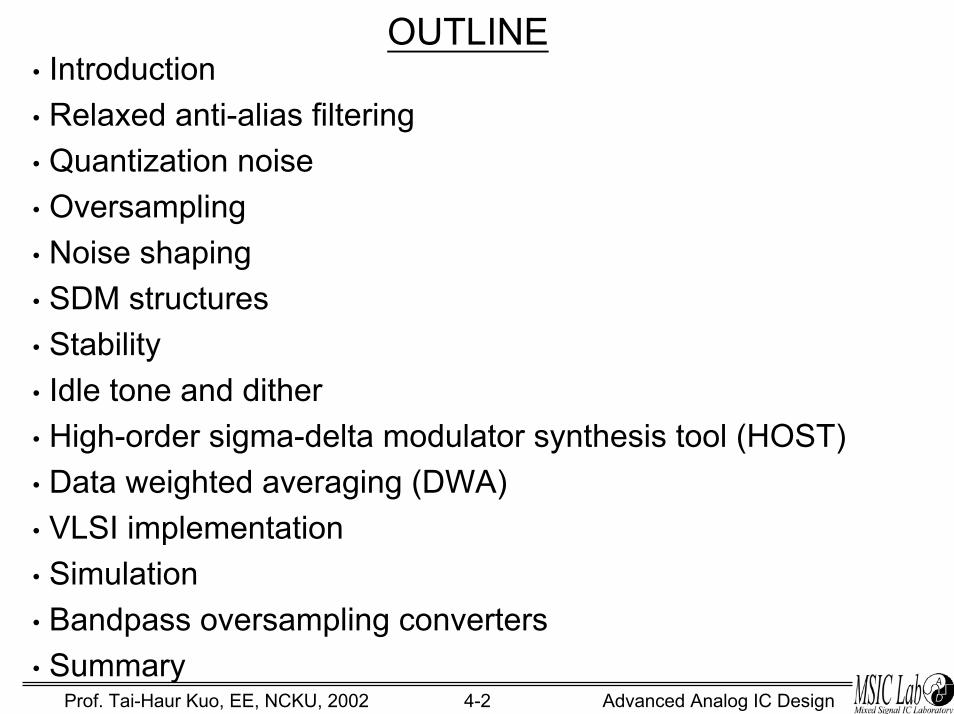
OUTLINE• Introduction• Relaxed anti-alias filtering• Quantization noise• Oversampling• Noise shaping• SDM structures• Stability• Idle tone and dither• High-order sigma-delta modulator synthesis tool (HOST)• Data weighted averaging (DWA)• VLSI implementation• Simulation• Bandpass oversampling converters• Summary

4-3Prof. Tai-Haur Kuo, EE, NCKU, 2002 Advanced Analog IC Design
Introduction• Delta-sigma ADC/DAC= Sigma-delta ADC /DAC= Oversampling ADC /DAC
• Developed three decades ago• Achieved commercial implementation due to recent
advances in mixed-mode analog-digital VLSI technology• Recently very popular for high-resolution medium-to-low
speed applications• Relax the requirements placed on the analog circuitry at the
expense of more complicated digital circuitry– This tradeoff becomes more desirable for modern
submicron technologies with 3.3V power supplies. (even lower voltage for deep submicron)1. Complicated high-speed digital circuitry is more
easily realized in less area

4-4Prof. Tai-Haur Kuo, EE, NCKU, 2002 Advanced Analog IC Design
Introduction (Cont.)2. High-resolution analog circuitry is complicated by
(i) low power supply voltages(ii) poor output impedance, caused by short-channel
effects3. Reduced requirements on matching tolerances and
amplifier gain– Simplify the requirements of analog anti-aliasing filters for
ADCs and smoothing filters for DACs (on chip or off chip)– S/H is usually not required at the input of an
oversampling ADC (internal integrators have the function)• Extra bits of resolution can be extracted from converters that
sample much faster than the Nyquist rates by spectrally shaping the quantization noise through the use of feedback.

4-5Prof. Tai-Haur Kuo, EE, NCKU, 2002 Advanced Analog IC Design
Delta-Sigma Market Potential• ADC revenue & conversion rate - 1989
• Estimated ADC revenue & conversion rate - 1994
Revenue(Millions of Dollars)
100 msec 10msec 1 msec 100 µsec 10 µsec 1 µsec 100 nsec 10nsec 1nsec
250200150100500
General-Purpose A/D Converters
Display ConvertersFlash Converters
Conversion Time
250200150100500
Revenue(Millions of Dollars)
100 msec 10msec 1 msec 100 µsec 10 µsec 1 µsec 100 nsec 10nsec 1nsec
Successive-Approximation ADCs
Display Converters
Delta-Sigma ADCs
Flash Converters
Conversion Time

4-6Prof. Tai-Haur Kuo, EE, NCKU, 2002 Advanced Analog IC Design
Applications
• Audio/Voice codec
• DVD
• High precision measurement
• ISDN
• ADSL
• Mobile (Cellular) phone
• Many others

4-7Prof. Tai-Haur Kuo, EE, NCKU, 2002 Advanced Analog IC Design
Brief Overview of Sigma-Delta A/D StructureSigma-delta ADC consists of two basic blocks
– Analog negative feedback loopOversamples & processes analog input
– Digital decimation filterPerform system-level filtering with performance unachievablein analog form
Structure of an N-bit ADC with an M-bit internal ADC and DAC
AnalogLP Filter
M-bitADC
Digital Decimation Filter
M-bitDAC
-+Analog
input
M-bit
N-bitDigital output

4-8Prof. Tai-Haur Kuo, EE, NCKU, 2002 Advanced Analog IC Design
Brief Overview of Sigma-Delta D/A StructureSigma-delta DAC consists of three blocks
– Digital interpolation filter
– Digital negative feedback loop
– Analog filter including digital-to-analog interface
Structure of an N-bit DAC with an M-bit internal quantizer
Digital interpolationFilter
Digital input
N-bit
Analog output
Analog FilterM-bitDigital
Quantizer
M-bitDigital LP Filter+
-

4-9Prof. Tai-Haur Kuo, EE, NCKU, 2002 Advanced Analog IC Design
OUTLINE• Introduction• Relaxed anti-alias filtering• Quantization noise• Oversampling• Noise shaping• SDM structures• Stability• Idle tone and dither• High-order sigma-delta modulator synthesis tool (HOST)• Data weighted averaging (DWA)• VLSI implementation• Simulation• Bandpass oversampling converters• Summary

4-10Prof. Tai-Haur Kuo, EE, NCKU, 2002 Advanced Analog IC Design
Signal Spectra of Zero-Width Samples• For zero-width sampling
Original signalSampled-data signal
– Spectrum of sampled signal)j(F)t(f
)j(F )t(f
ω→
ω→∗∗
∑∞
−∞=
∗ −=k T
jkjFT
jF )2(1)( πωω
Aω Bω
)j(FB ω
)j(FA ω
)j(F ω
)j(TF* ω Tπ
ω
• Continuous-time signals and
• Sample-data signals and
)t(fA
)t(f*A
)t(fB
)t(f*B
ωT2π
Tπ
)j(F B* ω
)j(F *A ω

4-11Prof. Tai-Haur Kuo, EE, NCKU, 2002 Advanced Analog IC Design
Nyquist Theorem• Replicas forming overlap
This phenomenon is called aliasing or folding.
It is a nonlinear distortion
• Low-pass filter
)j(F*B ω
)j(F)j(H)j(FT
||;0T
||;1)j(H
A*A ω=ωω
π>ω
π≤ω
=ω
– The continuous-time signal is recovered. But no such operation can regain from
– Nyquist first observed this phenomenonNyquist theorem
)j(F*B ω)j(FB ω
)t(fA

4-12Prof. Tai-Haur Kuo, EE, NCKU, 2002 Advanced Analog IC Design
Sampling• Nyquist theorem :
To avoid aliasing, sampling frequency must be at least twice of the signal to be sampled.
• Alias– Spectrum before sampling
– Spectrum after samplingfs/2
EnergyDensity
baseband fs
Nyquist rate = fs
Frequency
EnergyDensity Nyquist rate = fs
baseband fs/2
4-13Prof. Tai-Haur Kuo, EE, NCKU, 2002 Advanced Analog IC Design
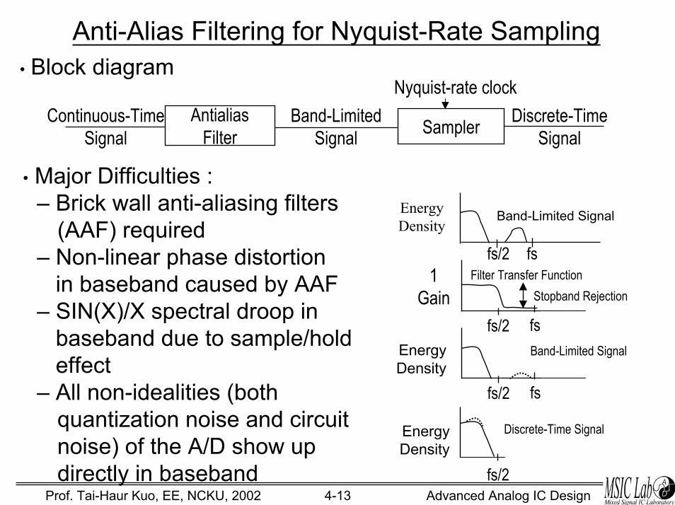
Anti-Alias Filtering for Nyquist-Rate Sampling• Block diagram
Discrete-TimeSignal
Nyquist-rate clockAntialias
Filter SamplerBand-LimitedSignal
Continuous-TimeSignal
• Major Difficulties : – Brick wall anti-aliasing filters
(AAF) required– Non-linear phase distortion
in baseband caused by AAF– SIN(X)/X spectral droop in
baseband due to sample/hold effect
– All non-idealities (both quantization noise and circuit noise) of the A/D show up directly in baseband
Filter Transfer Function
Band-Limited SignalEnergyDensity
fs/2 fs1
Gain Stopband Rejection
fs/2 fsEnergyDensity
Band-Limited Signal
fs/2 fs
Discrete-Time SignalEnergyDensity
fs/2

4-14Prof. Tai-Haur Kuo, EE, NCKU, 2002 Advanced Analog IC Design
Relaxed Anti-Alias Filtering for Oversampling Technique• Anti-aliasing
Continuous-Time Signal
EnergyDensity
fs/2 fs
• Digital filtering/decimation– High performance digital filter is required
fs/2 fs
Discrete-Time SignalEnergyDensity
Nfs
fs/2
1GainAnti-alias Filter Transfer Function
for Oversampling Conversion
NfsNfs-fs/2
fs/2fs/2
1Gain
EnergyDensityDigital Filter Transfer Function Nyquist Rate Digital Signal

4-15Prof. Tai-Haur Kuo, EE, NCKU, 2002 Advanced Analog IC Design
Conventional Conversion vs. Sigma-Delta Conversion
• Nyquist ADC (pules-code modulation, PCM)
Nyquist rateBandwidth=Nyquist rate/2
AnalogInput
Anti-aliasingfilter
PCMAnalog todigital
• Nyquist DAC
Bandwidth=Nyquist rate/2
Nyquist rate
Digital toanalog
Smoothingfilter
AnalogOutputPCM

4-16Prof. Tai-Haur Kuo, EE, NCKU, 2002 Advanced Analog IC Design
Sigma-delta ADC
•Conventional Conversion vs. Sigma-Delta Conversion (Cont.)
High speed clock
Digital Decimation
Filter
AnalogModulator
Analog Digital
PCMRegister Digital
ModulatorDigital
InterpolationFilter
Relaxed Smoothing
Filter
High speed clockNyquist rate
Digital Analog• Sigma-delta DAC
AnalogInput Relaxed Anti-
aliasing Filter Register
Nyquist rate
PCM
Analog Output

4-17Prof. Tai-Haur Kuo, EE, NCKU, 2002 Advanced Analog IC Design
OUTLINE• Introduction• Relaxed anti-alias filtering• Quantization noise• Oversampling• Noise shaping• SDM structures• Stability• Idle tone and dither• High-order sigma-delta modulator synthesis tool (HOST)• Data weighted averaging (DWA)• VLSI implementation• Simulation• Bandpass oversampling converters• Summary

4-18Prof. Tai-Haur Kuo, EE, NCKU, 2002 Advanced Analog IC Design
Quantization Noise• Random signal assumption qantization error e is uniformly distributed
between +LSB/2 and -LSB/2
3
-1
-3
-5
5
21 4-4 -2
y
x x
e
LSB
2LSB
2LSB
−
LSB1
probability density functionquantization errortransfer curve
• Qantization noise power and signal-to-noise ratio (SNR)
For a sinusoidal input, x t A t( ) sin( )= ω , A is full scale magnitude,∫∫−
=== ∞∞− LSB
1
LSB1 12
LSBdeeLSB
1de)e(pee2
222RMS
b is number of bit and , then peak SNR (PSNR)b2/A2LSB=
)( 76.102.6)12/
2/log(102/2
2
2
2
dBbLSB
AeA
PPPSNR
RMSNOISE
SIGNAL +====

4-19Prof. Tai-Haur Kuo, EE, NCKU, 2002 Advanced Analog IC Design
Quantization Noise Spectrum• White noise assumption power spectral density is constant
fsLSBfE 1
12)(
22 =
bS f2/f
OSR1
12LSB
ff2
12LSBP
2
S
b2
NOISE ==
E f2 ( )
eRMS2
eRMS2
eRMS2
– Quantization noise density is inversely proportional to the sampling rate– If signal bandwidth is and oversampling ratio OSR=
total noise in signal band =
22Sf−
21Sf− bf− bf 2
1Sf2
2Sf
bf
)dB( )OSRlog(1076.1b02.6PSNR ++=Doubling OSR increases 3dB SNR

4-20Prof. Tai-Haur Kuo, EE, NCKU, 2002 Advanced Analog IC Design
Limitation of Oversampling•
– S/N is improved by OSR
– LSB becomes smaller
– Resolution is increased by
• The problem with 1-bit (or even multi-bit) converters is that the desired resolution and bandwidth requires unreasonable oversampling ratios
OSR1
12LSBP
2
NOISE =
OSR
)(log2 OSR
13 Bits, 4KHz 1 Bit, 537GHz3 Bits, 134GHz
13 Bits, 144KHz 1 Bit, 19.3THz3 Bits, 4.8THz
16 Bits, 20KHz 1 Bit, 172THz3 Bits, 43THz
VOICE
ISDN
Digital HIFI

4-21Prof. Tai-Haur Kuo, EE, NCKU, 2002 Advanced Analog IC Design
OUTLINE• Introduction• Relaxed anti-alias filtering• Quantization noise• Oversampling• Noise shaping• SDM structures• Stability• Idle tone and dither• High-order sigma-delta modulator synthesis tool (HOST)• Data weighted averaging (DWA)• VLSI implementation• Simulation• Bandpass oversampling converters• Summary

4-22Prof. Tai-Haur Kuo, EE, NCKU, 2002 Advanced Analog IC Design
Sigma-Delta Modulation : Noise-Shaping + Oversampling
• Change the energy spectrum of quantization noise. Shift low frequency energy to high frequency stopband of decimation filter.
• Spectrum of sigma-delta ADCSigma-delta modulator
loop filter+-
D/A
Quantization noise
+
digital filter
digital digitalanalog
Anti-aliasing filter
analog
f
Input signal Modulator output Output signal

4-23Prof. Tai-Haur Kuo, EE, NCKU, 2002 Advanced Analog IC Design
Sigma-Delta Modulators• Block diagram E(z)
U(z) Y(z)+
+
)()()()()()(1
1)()(1
)()( zEzNTFzXzSTFzEzH
zXzHzHzY +=
++
+=
– H(z) : high-gain lowpass function– STF : Signal Transfer Function (lowpass)– NTF : Noise Transfer Fuction (highpass)
X(z)
H(z)ADC
DAC
Y(z)
E(z)
U(z)

4-24Prof. Tai-Haur Kuo, EE, NCKU, 2002 Advanced Analog IC Design
Noise Shaping• First-order sigma-delta modulator
• Discrete-time model D/A
-+y(n)x(n) + + +
e(n)
Accumulation Quantization
)Z)(z(EZ)z(X)z(Y
)n(e)n(e)n(x)n(y11 1
11−− −+=
−−+−=
• Effect of feedback on noise11 −− Z
fb fs/2
modulation noise, n
quantization error, e
– Frequency characteristic of
delay
2
-+ + ∫ A/D
CK
y(t)x(t)
1

4-25Prof. Tai-Haur Kuo, EE, NCKU, 2002 Advanced Analog IC Design
First-Order Sigma-Delta Modulator• Block diagram
E(z)
Z -1 ++
Y(z)X(z)+
++-
Y z z X z z E z( ) ( ) ( ) ( )= + −− −1 11
• Noise power in the baseband3223
S
b22
1ff
2RMSNOISE OSR
1312
LSBff2
312LSBdf)z1(eP b
b
π=
π=−= −−∫
• Doubling the OSR increases 9dB SNR(dB) OSRbPSNR )log(3017.576.102.6 +−+=

4-26Prof. Tai-Haur Kuo, EE, NCKU, 2002 Advanced Analog IC Design
Second-Order Sigma-Delta Modulator• Block diagram E(z)
• Noise power in the baseband
• Doubling the OSR increases 15dB SNR(dB) OSRbPSNR )log(509.1276.102.6 +−+=
Z -1-+ ++
X(z)+-
Y(z)
++
Z -1
)z(E)z1()z(Xz)z(Y 211 −− −+=
522542fbfb
212RMSNOISE OSR
1312
LSBfsfb2
512LSBdf)z1(eP
π=
π=−= ∫−
−

4-27Prof. Tai-Haur Kuo, EE, NCKU, 2002 Advanced Analog IC Design
Nth-Order Sigma-Delta Modulator• Block diagram
X(z)-
Z -1
Y(z)Z -1
E(z)
)z(E)z1()z(Xz)z(Y N11 −− −+=
• Noise power in the baseband
1N2N22
1N2N22fbfb
N12RMSNOISE
OSR1
1N212LSB
fsfb2
1N212LSBdf)z1(eP
+
+
−−
+π=
+π=−= ∫
Z -1- -
• Doubling the OSR increases 3(2N+1) dB SNR
(dB) OSRNbPSNR N
N
)log()12(10)2
log(1076.102.6 1
2
+−π
−+=+

4-28Prof. Tai-Haur Kuo, EE, NCKU, 2002 Advanced Analog IC Design
Noise-Shaping Characteristics of SDMs
N1
31
21
1
)z1(:orderNth
...
)z1(:orderrd3
)z1(:ordernd2
z1:orderst1
−
−
−
−
−−
−−
−−
−−
31/
fs/2

4-29Prof. Tai-Haur Kuo, EE, NCKU, 2002 Advanced Analog IC Design
Quantization Noise Power of 1-bit Modulators• 1-bit SDM output Y : ±1
Normalized power : 1 Watt• Y(n) consists of signal and quantization noise
Signal power can never be greater than 1 Watt• Example
peak signal is within ±0.25maximum signal power = 62.5mWquantization noise power = 1W – 62.5mW = 937.5mWsignal power is 12 dB below the quantization noise power
• The quantization noise power is mostly in a different region than the signal power and can therefore be filtered out.
• The filter must have a dynamic range capable of accommodating the full power at its input.

4-30Prof. Tai-Haur Kuo, EE, NCKU, 2002 Advanced Analog IC Design
OUTLINE• Introduction• Relaxed anti-alias filtering• Quantization noise• Oversampling• Noise shaping• SDM structures• Stability• Idle tone and dither• High-order sigma-delta modulator synthesis tool (HOST)• Data weighted averaging (DWA)• VLSI implementation• Simulation• Bandpass oversampling converters• Summary

4-31Prof. Tai-Haur Kuo, EE, NCKU, 2002 Advanced Analog IC Design
• Low-order SDMs (1st and 2nd order)– Higher OSR Signal bandwidth is limited – Serious tones in the baseband dither is required – Stable
Low-Order vs. High-Order SDMs
• High-order SDMs ( 3rd order)– Lower OSR required to achieve the same SNR – Less tones in baseband (quantization noise is more random)– Instability problems
1. Complicated design for a stable modulator2. Smaller stable input range
– High SNR and DR
≥

4-32Prof. Tai-Haur Kuo, EE, NCKU, 2002 Advanced Analog IC Design
High-Order SDM Structures• Multi-stage noise shaping (MASH) structure
– Cascaded first-order modulator1+1+1 SDM, 1+1+1+1 SDM
– Cascaded first-order and/or second-order modulator2+1 SDM, 2+2 SDM
• Single-stage structure– Feedforward (FF) modulator– Multiple-feedback (MF) modulator– Others

4-33Prof. Tai-Haur Kuo, EE, NCKU, 2002 Advanced Analog IC Design
MASH ( Cont. )• 1+1+1 structure
H(Z)
X(z) H(Z)
H(Z)
-
-
-
-
E 2
E1
E 3
Analog
+
-
+
+
Y z z X z z E z( ) ( ) ( ) ( )= + −− −3 1 331
where 1
1
z1z)z(H −
−
−=
z -1
z -1 -+
z -1
z -1
z -1 -+
z -1 -+
++
Y(z)
++
Digital

4-34Prof. Tai-Haur Kuo, EE, NCKU, 2002 Advanced Analog IC Design
MASH (Cont.) • 2+1 structure
H(Z)H(Z) -
H(Z)-
-
E1
E2+
++ ++
2
)z(E)z()z(Xz)z(Y 2313 1 −− −+=
-
z -1
+z -1
+-
z -1 +Y(z)X(z) +
-
Analog Digital

4-35Prof. Tai-Haur Kuo, EE, NCKU, 2002 Advanced Analog IC Design
MASH (Cont.)• Advantages
– Stable (composed of low-order SDMs)– Structure design is easier (compared with single-stage)
• Disadvantages– Requirement of better components matching
Sensitive to finite OPAMP gain and mismatches between the analog and digital circuitry.Such mismatches cause first-order noise to leak through from the first modulator and hence reduce dynamic range. To alleviate this mismatch problem, often the first stage is chosen to be a higher order modulator
– Usually, order ≤4 (limited by mismatch) for ADC
4-36Prof. Tai-Haur Kuo, EE, NCKU, 2002 Advanced Analog IC Design
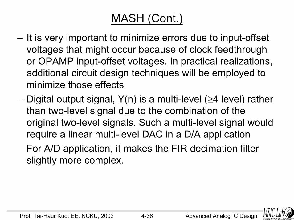
MASH (Cont.)– It is very important to minimize errors due to input-offset
voltages that might occur because of clock feedthrough or OPAMP input-offset voltages. In practical realizations, additional circuit design techniques will be employed to minimize those effects
– Digital output signal, Y(n) is a multi-level (≥4 level) rather than two-level signal due to the combination of the original two-level signals. Such a multi-level signal would require a linear multi-level DAC in a D/A applicationFor A/D application, it makes the FIR decimation filter slightly more complex.

4-37Prof. Tai-Haur Kuo, EE, NCKU, 2002 Advanced Analog IC Design
Commonly Used Single-Stage SDM Structures• Feedforward (FF)
• Multiple-feedback (MF)
g1 H2g2 g3 H3
bm
+
- -an-2an-1an
-x(z) H1
b1
gn-1 Hngn-
a1a2
- -Hn-1
y(z)
D/A
H1g1 H2g2
-g3 H3
b1 bm
Hn-1gn-1 Hngn an
an-1
+
-+
y(z)+
-x(z)
a2 a1 D/A
+

4-38Prof. Tai-Haur Kuo, EE, NCKU, 2002 Advanced Analog IC Design
• Advantages– Less component matching requirement (compared with MASH
architechures)– Very high resolution (very high order is achievable)
Single-Stage SDMs
• Main problems – Instability of high-order SDMs
Instability recovery machanism is required– Complicated design for a stable high-order modulator
Efficient design tool for high-order SDMs is required

4-39Prof. Tai-Haur Kuo, EE, NCKU, 2002 Advanced Analog IC Design
OUTLINE• Introduction• Relaxed anti-alias filtering• Quantization noise• Oversampling• Noise shaping• SDM structures• Stability• Idle tone and dither• High-order sigma-delta modulator synthesis tool (HOST)• Data weighted averaging (DWA)• VLSI implementation• Simulation• Bandpass oversampling Converters• Summary

4-40Prof. Tai-Haur Kuo, EE, NCKU, 2002 Advanced Analog IC Design
Stability Criteria• A stable modulator is defined here, as one in which the input
to the quantizer remains bounded such that the quantization does not become overloaded.Overloaded quantizer: quantization error greater than ±LSB/2
• The stability of higher-order modulator is not well understood as they include a highly nonlinear element (especially low-bit quantizer).
• Stability criteria1. Rule of thumb for stable SDM
for This stability criterion has little rigorous justification.
2. 1-norm stability criterion,It’s often too conservative, as it eliminates many stablemodulators.
5.1)e(NTF jw < πw0 < <
max,in2f0
s1 X3df)f(NTF
f2NTF s
−<∫=

4-41Prof. Tai-Haur Kuo, EE, NCKU, 2002 Advanced Analog IC Design
Stability Criteria(Cont.)3. 2-norm stability criterion
– Numerical simulation can be used to find stability bounds– Useful stability bounds for single-stage SDMs are first
proposed by T.H. Kuo and K.D. Chen, EE, NCKU, Taiwan ( IEEE Trans. CAS-II, Jan. 1999)
Pin= for sinwaves with a amplitude of A
Increase SDM order
Pin
NPGStability bounds
less stablelarger PSNRsmaller Pin(max)
– Larger NPG
∫== 2f0
2
S
22
s df)f(NTFf2)f(NTFNPG
2/A2
where

4-42Prof. Tai-Haur Kuo, EE, NCKU, 2002 Advanced Analog IC Design
Instability Recovery• Instability detection(two commonly used methods)
1. Looking for long strings of 1s or 0s at the SDM output.2. Monitoring signal amplitude at the quantizer input to see
if predetermined amplitude thresholds are exceeded for aspecified number of consecutive clock cycles.
• Instability recovery (Circuit is changed to force an unstableSDM back to its stable state) Three methods:
1. Reset all integrator outputs to zero Reset
circuitReset
circuit
Reset
circuit
G1 G2 G3H1 H2 H3
D/A
OverloadDetector
U1 U2 U3
X(z) Y(z)U1 U2 U3
•
• •
•• •
• •

4-43Prof. Tai-Haur Kuo, EE, NCKU, 2002 Advanced Analog IC Design
Instability Recovery2. Change the SDM into a 2nd-order or even first-order SDM
by using only the first two integrators and resetting others.
•
G1 G2 G3H1 H2 H3U1 U2
U3
MUX1
2
D/A
Resetcircuit
OverloadDetector
U1U2U3
If overloaded, switch from 1 to 2
X(z)
•
•
•
•
•
• Y(z)

4-44Prof. Tai-Haur Kuo, EE, NCKU, 2002 Advanced Analog IC Design
Instability Recovery(cont.)3. Eliminate the comparator temporarily from the high-order
integrators. This changes the modulator into a modulator-filter combined SDM. This technique is called internal linear feedback(ILF). Invented by T.H. Kuo and W.C.Wang, etc., EE, NCKU, Taiwan.(US patent No. 5,742,246, 1998)
– “3” is the best. “1” and “2” lose information due to reset.– Multi-bit SDMs exhibit improved stability over their 1-bitcounterpart.
Y(z)G1 G2H1 H2 G3 H3X(z) Gn Hn
oo
D/A
OverloadDetector
ILF
normal
+ + ++ •
••
•
4-45Prof. Tai-Haur Kuo, EE, NCKU, 2002 Advanced Analog IC Design
OUTLINE• Introduction• Relaxed anti-alias filtering• Quantization noise• Oversampling• Noise shaping• SDM structures• Stability• Idle tone and dither• High-order sigma-delta modulator synthesis tool (HOST)• Data weighted averaging (DWA)• VLSI implementation• Simulation• Bandpass oversampling Converters• Summary

4-46Prof. Tai-Haur Kuo, EE, NCKU, 2002 Advanced Analog IC Design
Idle Tone• Examples:
1. apply a dc level of 1/3 to a 1st-order SDM having a 1-bitquantizer with output levels of 1modulator output =⇒ idle tone at can be filtered by lowpass postfilter
2. apply a dc level of 3/8 to the same modulatormodulator output =⇒ idle tone at may not be filtered by lowpass
postfilter • Higher-order SDM ⇒ less idle tone• Tones might not lie at a single frequency but instead be
short-term periodic patterns. In other words, a tone appearing near 1KHz might actually be a signal varying between 900Hz and 1.1KHz in a random-like fashion.
±
{ }.....1,1,11,1,1,1,1,1,1,1 −−−
{ },....1,1,1,1,1,1,1,1,1,1,1,1,1,1,1,1,1,1,1 −−−−−−
16fS
3fS

4-47Prof. Tai-Haur Kuo, EE, NCKU, 2002 Advanced Analog IC Design
Dithering• One way to reduce the amount of idle tones in modulators
through the use of dithering. The term dithering here refers to the act of introducing some random(or pseudo-random) signal into a modulator.
• The most suitable place to add the dithering signal is just before the quantizer. Thus, the dithering signal becomes noise shaped in the same manner as the quantization noise, and therefore a large amount of dithering can be added.
• Typically, the dithering signal is realized using some sort of pseudo-random number generator with only a few bits of resolution, but its total noise power is comparable to the quantization noise power.

4-48Prof. Tai-Haur Kuo, EE, NCKU, 2002 Advanced Analog IC Design
Dithering(cont.)• The use of dither to reduce idle tones is not an attempt to
add noise to mask out the tones but instead breaks up the tones so that they never occur.
• Since the noise power of the dithering signal is similar to the quantization noise power, the use of dithering adds about 3dB extra inband noise and often requires rechecking the modulator’s stability.
H(z) •
dither quantizer
X(z) Y(z)+

4-49Prof. Tai-Haur Kuo, EE, NCKU, 2002 Advanced Analog IC Design
OUTLINE• Introduction• Relaxed anti-alias filtering• Quantization noise• Oversampling• Noise shaping• SDM structures• Stability• Idle tone and dither• High-order sigma-delta modulator synthesis tool (HOST)• Data weighted averaging (DWA)• VLSI implementation• Simulation• Bandpass oversampling Converters• Summary

4-50Prof. Tai-Haur Kuo, EE, NCKU, 2002 Advanced Analog IC Design
HOST - High-Order SDM Synthesis Tool• HOST was developed by T.H. Kuo, K.D. Chen and J.R. Chen,
EE, NCKU, Taiwan.(Copyright No. 8702035,1998)HOST is the world first single-stage SDM synthesis tool.
• Automatic coefficient design of feedforward (FF) and multiple feedback (MF) SDMs
• Main features– Stable high-order SDMs with high tolerance coefficients– Optimization among SNR, OSR, order, coefficient
sensitivity, quantization levels, and stability of a SDM – SDMs can be synthesized for various specifications.– Low baseband tones and harmonics

4-51Prof. Tai-Haur Kuo, EE, NCKU, 2002 Advanced Analog IC Design
A Design Example Using HOST• Audio specifications
– SNR (Dynamic Range) > 16 bit = 96dB– Oversampling ratio (OSR) =64– Baseband bandwith = 22.5kHz– Modulator order =4 – Maximum stable input > -6dB– Bit number of internal quantizer = 1– Feedforward structure
• Synthesized modualtor coefficientsb1=0.083209 b2=0.013754
g1=0.575769 g2=0.629813g3=0.308405g4=0.083209
a1=1.276899 a2=0.710255a3=0.452129a4=0.480403

4-52Prof. Tai-Haur Kuo, EE, NCKU, 2002 Advanced Analog IC Design
Simulation Results• Noise transfer function(NTF) Poles and zeros of NTF
• Output spectrum • Dynamic range plot

4-53Prof. Tai-Haur Kuo, EE, NCKU, 2002 Advanced Analog IC Design
OUTLINE• Introduction• Relaxed anti-alias filtering• Quantization noise• Oversampling• Noise shaping• SDM structures• Stability• Idle tone and dither• High-order sigma-delta modulator synthesis tool (HOST)• Data weighted averaging (DWA)• VLSI implementation• Simulation• Bandpass oversampling Converters• Summary

4-54Prof. Tai-Haur Kuo, EE, NCKU, 2002 Advanced Analog IC Design
Conversion Errors of Internal ADC and DAC• Block Diagram of analog SDM
• Internal A/D conversion errors can be attenuated by NTF at the baseband
• Internal D/A conversion errors are regarded as input signal ( without any attenuation at the baseband )
X(z)ADC
DAC
H(z) Y(z)
Eadc(z)
U(z)
Edac(z)[ ] )z(Eadc
)z(H11)z(Edac)z(X
)z(H1)z(HY
+++
+=
•

4-55Prof. Tai-Haur Kuo, EE, NCKU, 2002 Advanced Analog IC Design
One-Bit vs. Multi-Bit Analog SDMs• 1-bit DAC (only two level) is perfect linear
– Major motivation for SDMs to use 1-bit internal DAC(and hence 1-bit internal ADC)
– Many 16-18 bits audio converters presently use 1-bit internal DAC.
• Multi-bit DAC requires good component matching for high-resolution For a 16-bit resolution converter, components mismatch forinternal DAC must be less than %0015.02/1 16 =

4-56Prof. Tai-Haur Kuo, EE, NCKU, 2002 Advanced Analog IC Design
Multi-Bit Analog SDMs• Multi-bit internal ADC or DAC
– Quantization noise (smaller compared with 1-bit converters)
– Offset error (can be ignored for SDM)
– Gain error (can be ignored for SDM)
– Nonlinearity error (introduces harmonic distortions)
Y (analog output)
00 01 10 11X(digital code)
Transfer curve32 dxcxbxay +++=

4-57Prof. Tai-Haur Kuo, EE, NCKU, 2002 Advanced Analog IC Design
Multi-Bit Analog SDMsMotivations of development for multibit sigma-delta converters– High speed applications (low OSR)– Enhancement of modulator stability– Relax post analog filter design of sigma-delta DACs.
• Multibit SDMs become popular due to the development of techniques for reducing DAC nonlinearity effect – Many methods (shown in the next page)
IDWA is the best, up to now, among them– Improved Data weighted averaging (IDWA) algorithm
1. First-order DAC-noise shaping (ideally)2. Most efficient on attenuation of DAC noise3. Lowest cost for implementation

4-58Prof. Tai-Haur Kuo, EE, NCKU, 2002 Advanced Analog IC Design
Techniques for Overcoming DAC Linearity Problem
• Changed SDM architectures (ISCAS’90,JSSC’91)• Self-calibration technique (JSSC’91)• Digital correction (JSSC’93)• Dynamic element matching, DEM
– Randomization (JSSC’89)– Clock averaging (TCAS-II’92) – Individual level averaging (TCAS-II’92)– Data weighted averaging (‘93 patent : Motolora)– Data-directed scrambling (‘95 patent : Analog Device)– Second-order data weighted averaging (ISCAS’96)– Grouped-level averaging (ISSCC’98)– Tree structure noise shaping dynamic element
matching (ISSCC’98)

4-59Prof. Tai-Haur Kuo, EE, NCKU, 2002 Advanced Analog IC Design
Data Weighted Averaging• Using elements at maximum possible rate ensures that the DAC errors will
quickly sum to zero, moving distortion to high frequencies− Example : 8 - level (7- element), i.e. 3-bit, DAC
)z(NDAC
1
11
z1zg
−
−
− 1
12
z1zg
−
−
− 1
12
z1zg
−
−
−
1b
3a2a1a
)z(x
−−
N-level
DAC)z(Y
)z(NADC
H(z) 1C 2C 3C 4C 5C 6C 7CAnalog output
GroundrefV
Time slot n n+1 n+2 n+3 n+4 n+5
DAC input code, y(n) 3 4 0 2 5 3
pointer position, ptr(n) 4 1 1 3 1 4
selected elements C1 C4 C1 C3 C1
C2 C5 C2 C4 C2
C3 C6 C5 C3
C7 C6
C7

4-60Prof. Tai-Haur Kuo, EE, NCKU, 2002 Advanced Analog IC Design
Data Weighted Averaging (Cont.)Example : a third-order SDM with a 8 level DAC− SDM output spectrum
improved DWA(1% mismatch)
DAC with 1% elements mismatch (without DWA)ideal DAC DWA (1% mismatch)
Limitation of conventional DWA– Aliasing tones in the basebandThis problem can be resolved by– Adding dither at the expense of noise level increase– Using an improved DWA proposed by K.D.Chen and T.H.Kuo,
EE, NCKU,Taiwan (IEEE Trans. CAS-II, Jan. 1999, ROC patent approved, US patent pending)
Aliasing tones

4-61Prof. Tai-Haur Kuo, EE, NCKU, 2002 Advanced Analog IC Design
Practical Considerations of Two-Level D/A Converters• Nonidealities of two-level D/A converters
(can also be applied to multi-level converters)1. power supply bounce2. switch feedthrough is signal dependent, e.g.
when more 1s than 0s are being output by the D/A converter.⇒ Well-regulated power-supply voltages on the drivers for
the input switches is very important. 3. clock jitter
71

4-62Prof. Tai-Haur Kuo, EE, NCKU, 2002 Advanced Analog IC Design
Practical Considerations of Two-Level Converters (Cont.)4. memory between output levels
A nonreturn-to-zero(NRZ) 1-bit DAC typical output
TypicalIdealV2
V1
1 -1BinaryArea forSymbol 11A δ+
111 --1 1
1A 20A δ+ 20A δ+0A 11A δ+ 11A δ+
72

4-63Prof. Tai-Haur Kuo, EE, NCKU, 2002 Advanced Analog IC Design
Practical Considerations (Cont.)Example: three periodic patterns corresponding to average voltages of 0,1/3,and -1/3 when V1 and V2 are 1V
These three averages don’t lie on a straight line except
Thus, one way to obtain high linearity is to match falling and rising signals. This is a very difficult task since they aretypically realized with different types of devices.
±
{ }2
)(2
)(.....1-,1,1-,1:0 212101 δδδδ ++=
+++=⋅⋅ tVAAtV ad
{ }3
)t(V3
AA2)t(V→.....1-,1,1:3/1 21b
2101e
δ+δ+=
δ+δ++=
{ }3
)t(V3
A2A)t(V→.....1,1-,1-:3/1 21c
2101f
δ+δ+=
δ+δ++=−
21 δ−=δ
73

4-64Prof. Tai-Haur Kuo, EE, NCKU, 2002 Advanced Analog IC Design
Practical Considerations (Cont.)– Memoryless coding scheme
e.g. return-to-zero coding scheme
• Switch capacitor circuits naturally realize memoryless levels as long as enough time is left for settling one each clock phase.Thus, the first stage of postfiltering in oversampling D/A converters is often realized using SCFs, which is followed by continuous-time filtering.
V1
V2Ideal
Binary 1 -1 1-11 -1-1
1A 1A1A0A0A1A 0A
Typical
Area forSymbol
74

4-65Prof. Tai-Haur Kuo, EE, NCKU, 2002 Advanced Analog IC Design
OUTLINE• Introduction• Relaxed anti-alias filtering• Quantization noise• Oversampling• Noise shaping• SDM structures• Stability• Idle tone and dither• High-order sigma-delta modulator synthesis tool (HOST)• Data weighted averaging (DWA)• VLSI implementation• Simulation• Bandpass oversampling Converters• Summary

4-66Prof. Tai-Haur Kuo, EE, NCKU, 2002 Advanced Analog IC Design
System Architectures of Sigma-Delta ADCs• Block diagram
– S/H is merged to SDM– Decimator ( OSR) is merged to digital LPF
)(nxs)(fxsh )(nxlp)(nxdsm)f(xc)f(xln
Sample-and-hold
SDMDigital
low-passfilter
OSR
Digital decimation filtersf sf sf
Analog modulator
Anti-aliasing
filter02f
Analog Digital

4-67Prof. Tai-Haur Kuo, EE, NCKU, 2002 Advanced Analog IC Design
System Architectures of Sigma-Delta ADCs (Cont.)• Signals and spectra
)(txc )(txsht
n
n
1)n(xdsm ±=
)n(xlp
34
3
)f(xc
f
ω
ω
ω
0f sf
0f sf
)f(xsh
)(xlp ω
)(xs ω
)(xdsm ω
s0 f/f2π
s0 f/f2π
π2
π2
π π4π2 π6 π8 π10 π12n
)n(xs
2 31
f
12
12

4-68Prof. Tai-Haur Kuo, EE, NCKU, 2002 Advanced Analog IC Design
System Architectures of Sigma-Delta ADCs (Cont.)• Since digital circuitry is linear, the overall linearity is most
strongly dependent on realizing a linear DAC inside the sigma-delta modulator.Nonlinearity in the internal ADC have only a small effect on the linearity of the overall ADC, since the high gain in the feedback loop compensates for that nonlinearity

4-69Prof. Tai-Haur Kuo, EE, NCKU, 2002 Advanced Analog IC Design
System Architectures of Sigma-Delta DACs• Block diagram
– Interpolator ( OSR) is merged to digital LPF– M-bit D/A is usually merged to analog LPF
( )nxs )n(xdsm)n(xlp)n(x 2s )f(xda )f(xc
Analoglow-pass
filter
M-bitD/A
sf
Analog filter
Digitallow-pass
filterOSR
0f2 sf
Digital interpolation filter
DigitalSDM
sf
Digital Analog0
s
f2fOSR =

4-70Prof. Tai-Haur Kuo, EE, NCKU, 2002 Advanced Analog IC Design
System Architectures of Sigma-Delta DACs (Cont.)• Signals and spectra
)(xs ω
ω
ω
ω
ω
f
f
π π4π2 π6 π8 π10 π12
)(x 2s ω
)(xlp ω
)(xdsm ω
)(fxda
)f(x c
Frequency0f sf
0f sf
π2
π2
π2s0 f/)f2( π
s0 f/)f2( π
s0 f/)f2( π
)n(xs )n(x 2s
2 3 )1()2( )3( n
n
t,n
t
)n(xlp
2 3
)n(xdsm )f(xds
)f(xc
Time
1
1

4-71Prof. Tai-Haur Kuo, EE, NCKU, 2002 Advanced Analog IC Design
System Architectures of Sigma-Delta DACs (Cont.)• 1-bit internal D/A has excellent linearity.
Multi-bit internal D/A can reduce analog filter’s complexity. However, it’s linearity problem must be resolved.
• The order of the analog filter should be at least one order higher than that of the SDM.This analog filter should be linear so it does not modulate the noise back to the frequency band of interest.In many applications, the realization of those filters, especially if they are integrated, is nontrivial.

4-72Prof. Tai-Haur Kuo, EE, NCKU, 2002 Advanced Analog IC Design
Circuit Implementation of Sigma-Delta ADCs and DACs• Simple anti-aliasing filter• Analog modulator
– Switched-capacitor circuits : 1. Analog signal sampling, integration, delay, and scaling2. Feedback DAC
– Cmparators : 1-bit or multi-bit analog quantizer– Realization for high-resolution is difficult
• Digital filters– Application specific architecture– FIR/IIR filter : decimation (ADC) and interplolation (DAC)– Fast logic circuits for operation of multiplication and
addition
4-73Prof. Tai-Haur Kuo, EE, NCKU, 2002 Advanced Analog IC Design
Circuit Implementation of Sigma-Delta ADCs and DACs(cont.)
• Digital modulator– Simplification of multiplication and addition is required due
to its high throughput rate.Power-of-two coefficients are usually used.
– Digital quantization– Its function is similar to that of the analog SDM but it is
implemented using digital circuits.• Analog filter
– At least one-order higher than that of the digital modulator– Realization for high performance, especially if it is
integrated, is difficult.

4-74Prof. Tai-Haur Kuo, EE, NCKU, 2002 Advanced Analog IC Design
Example:SC Realization of a First-Order SDM for ADC(Example with single-ended OPAMP and 1-bit internal DAC)• Block diagram
1-bit D/A
U(n)y(n)
Analog Digital
Quantizer
H(z)
1z −
• Switched-capacitor (SC) implementation
Comparator
outV
Latch on falling2φ
2φ1φ
1φ2φ
C
)(, 12 φφ
)(, 21 φφ
inV
2/Vref
high V, out21 ↔φφ
low V)(),( out21 ↔φφ
– using only one input capacitor
Comparator
outV
Latch on falling2φ
2φ1φ
1φ2φ
C
inV
2Vref
2Vref−
– using only one reference voltage
CC
highV2/V outref ↔−lowV2/V outref ↔
C

4-75Prof. Tai-Haur Kuo, EE, NCKU, 2002 Advanced Analog IC Design
Digital Decimation Filters for Sigma-Delta ADCs• Two popular approaches : multi-stage and single-stage• Multi-stage
– a sinc FIR filter followed by an IIR filter1. sinc FIR filter : fast and simple2. IIR filter : low cost and large out-of-band attenuation,
but nonlinear phase
Lth-order
modulator∆Σ
IIR filter(+Sinc compensation)
Rate = 2 f0Rate = 8 f0Rate = fsTsinc(z) TIIR(z)
filterFIRSinc 1L+

4-76Prof. Tai-Haur Kuo, EE, NCKU, 2002 Advanced Analog IC Design
Digital Decimation Filters for Sigma-Delta ADCs (Cont.)– a sinc FIR filter followed by half-band filters
half-band FIR : (1) linear phase(2) coefficients are symmetric (3) every second coefficients are zero
Rate = fs
Lth-order
modulator∆Σ Tsinc(z) H1(z)
Rate = 4 f0
H2(z)
Rate = 2 f0 Rate = 2 f0Rate = 8 f0
H3(z)
Sinc compensation
FIR filterfilterFIR
Sinc 1L+Halfband FIR filters

4-77Prof. Tai-Haur Kuo, EE, NCKU, 2002 Advanced Analog IC Design
Digital Decimation Filters for Sigma-Delta ADCs (Cont.)– Realization of Sinc FIR
Sinc filter : averaging filterSinc for Lth-order SDMExample : average-of-M sinc filter
1L +
)z1z1(
M1z
M1)z(Sinc 1
M1M
0i
i−
−−
=
−
−
−== ∑
1L1LM1L
11L
M1)z1()
z11()z(Sinc
+++
−+ −
−=

4-78Prof. Tai-Haur Kuo, EE, NCKU, 2002 Advanced Analog IC Design
Digital Decimation Filters for Sigma-Delta ADCs (Cont.)Two approaches: (a) downsampling after filtering
(b) downsampling before differentiatorswhere (b) is more efficient (lower speed)
1z− 1z− Mz Mz
Out
M1
(Integrators) Differentiators
− −
1z− 1z− 1z− 1z−
Out
M1
− −
0f 0f M/f0 M/f0
(Operate at low clock rate)(Operate at high clock rate)

4-79Prof. Tai-Haur Kuo, EE, NCKU, 2002 Advanced Analog IC Design
Digital Decimation Filters for Sigma-Delta ADCs (Cont.)• Single-stage
– Example: a 2048-tap FIR was used to decimate 1-bit outputs from SDMs
1. No multi-bit multiplications are needed, since the input is simply 1-bit.
2. 2048 additions are required during one clock cycle at the Nyquist rate.If the Nyquist rate is 48KHz, a single accumulator would have to be clocked at 98.3MHz

4-80Prof. Tai-Haur Kuo, EE, NCKU, 2002 Advanced Analog IC Design
Comparison Four Sigma-Delta DAC Structures• Type 1
• Type 2
• Type 3
• Type 4
FIR X2Lowpass
FIR X2Lowpass
FIR X16Lowpass
Fourth order Multiple
Feedback SDM
FIR X2Lowpass
FIR X2Lowpass
FIR X16Lowpass
FIR X2Lowpass
FIR X2Lowpass
FIR X2Lowpass
FIR X8Lowpass
FIR X2Lowpass
FIR X2Lowpass
FIR X2Lowpass
FIR X8Lowpass
fifth order Multiple
Feedback SDM
Fourth order Multiple
Feedback SDM
fifth order Multiple
Feedback SDM
x
x
x
x
Y
Y
Y
Y
0f
0f
0f
0f
02f
02f
02f
02f
04f
04f
04f
04f
08f
08f
064f
064f
064f
064f
064f
064f
064f
064f
Structure Type SNR(dB) DR(dB) Arithmetic complexity Type 1 100 97 30 Type 2 108 105 30 Type 3 101 96 42 Type 4 111 105 42

4-81Prof. Tai-Haur Kuo, EE, NCKU, 2002 Advanced Analog IC Design
OUTLINE• Introduction• Relaxed anti-alias filtering• Quantization noise• Oversampling• Noise shaping• SDM structures• Stability• Idle tone and dither• High-order sigma-delta modulator synthesis tool (HOST)• Data weighted averaging (DWA)• VLSI implementation• Simulation• Bandpass oversampling Converters• Summary

4-82Prof. Tai-Haur Kuo, EE, NCKU, 2002 Advanced Analog IC Design
Simulation• System simulation in frequency / Z domain
– MATLAB/C/Fortran– ADC(analog modulator+digital decimation filter)
DAC(digital interpolation filter+digital modulator+analog filter)1. Signal-to-noise ratio (SNR) and dynamic range (DR)2. Gain3. Phase or group delay4. Coefficient quantization => minimum wordlength required

4-83Prof. Tai-Haur Kuo, EE, NCKU, 2002 Advanced Analog IC Design
Simulation(Cont.)• Time-domain behavior simulation
– MATLAB/C/Fortran– Modulator
1. Stability2. Overload for analog SDM (overflow for digital SDM) 3. Coefficient scaling4. Idle tone5. Effects of analog impairments for analog SDM6. Signal-to-(noise+distortion) ratio (SNDR) and DR
– Digital filter1. Truncation/rounding : finite wordlength2. Transient response3. Overflow
• Circuit and logic simulation– Spice and logic simulator

4-84Prof. Tai-Haur Kuo, EE, NCKU, 2002 Advanced Analog IC Design
Analog Impairments for Modulator Simulation• Analog impairments
– Operational amplifier: finite gain, finite bandwidth, slew rate limitation, limited swing, offset, nonlinearity, input-referred noise, output resistance
– Comparator: offset, hysteresis, speed, gain– Capacitor: matching, voltage coefficient– Switch: nonlinear turn-on resistance, thermal noise, clock
feedthrough, charge injection– Clock jitter
• Analysis and modeling of impairments• Approximation and simulation• Noise coupling (node-to-node, transistor-to-substrate-to-
transistor)

4-85Prof. Tai-Haur Kuo, EE, NCKU, 2002 Advanced Analog IC Design
Simulation Examples: Effects of Analog Impairments for Analog SDM
• Finite opamp gain • Finite slew rate
• Many others

4-86Prof. Tai-Haur Kuo, EE, NCKU, 2002 Advanced Analog IC Design
OUTLINE• Introduction• Relaxed anti-alias filtering• Quantization noise• Oversampling• Noise shaping• SDM structures• Stability• Idle tone and dither• High-order sigma-delta modulator synthesis tool (HOST)• Data weighted averaging (DWA)• VLSI implementation• Simulation• Bandpass oversampling Converters• Summary

4-87Prof. Tai-Haur Kuo, EE, NCKU, 2002 Advanced Analog IC Design
Bandpass Oversampling Converters• For IF signal processing
Signals are in a small amount of bandwidth, but have been modulated by higher-frequency carrier.– STF: bandpass– NTF: bandreject
Bandpass function
H(z)
bandpass
digital filter
of
fc
• Output signal
Quantization noise
fc
+Input signal
Quantizer
fc
offc
fc

4-88Prof. Tai-Haur Kuo, EE, NCKU, 2002 Advanced Analog IC Design
Bandpass Oversampling Converters(Cont.)• For lowpass SDMs, H(z) is lowpass and has a high gain
near DC, thus quantization noise is small around DC.• For bandpass SDMs, H(z) is bandpass and has a high gain
near fc, thus quantization noise is samll around fc,
and therefore most of the quantization noise can be removed through the use of a narrow bandpass filter of total width fO following the modulator.
• In the case of a bandpass ADC intended for digital radio, post digital filtering would remove quantization noise as well as adjacent radio channels.
• The oversampling ratio for a bandpass converter is fs/(2fo) and does not depend on the value of fc.

4-89Prof. Tai-Haur Kuo, EE, NCKU, 2002 Advanced Analog IC Design
Bandpass Oversampling Converters(Cont.)
• Application example: a 2nd-order bandpass SDM with a sampling frequency fs=4fc
– NTF zeros
f 200f2
OSR0s ==
o--zeroMHzfs 14 =
f2 0
2fs
KHz10f0 =
MHz4fs =
dc
f 200f2
OSR0s ==
MHz14fs =
2fs
dc
MHz4fs =
KHz10f0 =
1st-order lowpass SDM 2nd-order bandpass SDM

4-90Prof. Tai-Haur Kuo, EE, NCKU, 2002 Advanced Analog IC Design
Bandpass Oversampling Converters(Cont.)• Block diagram
1. For a 1st-order lowpass SDMH(z)=z-1/(1- z-1) NTF zero(i.e. H(z) pole)=1 (DC)
2. For a 2nd-order bandpass SDM H(z)= z-1/(1+ z-2)NTF zeros(i.e. H(z) poles)=j, -j
1Z−
1Z−
H(z)
+ + •
Quantizer
X(z) Y(z)•

4-91Prof. Tai-Haur Kuo, EE, NCKU, 2002 Advanced Analog IC Design
Bandpass Oversampling Converters(cont.)• Hence, the dynamic range increase of a 2nd-order bandpass
converter equals that of a first-order lowpass converter thatalso has only one zero at DC.Specifically, the dynamic range increase of a 2nd-orderbandpass converter is 1.5bits/octave or, equivalently,9dB/octave.To obtain the equivalent dynamic range increase of a 2nd-order lowpass converter, a fourth-order bandpass converter would have to be used.

4-92Prof. Tai-Haur Kuo, EE, NCKU, 2002 Advanced Analog IC Design
SummaryThe benefits from oversampling combined with noise shapingare substantial
They are likely to continue to replace high-resolution Nyquistrate converters in many applications with signal bandwidth upto several MHz range, particularly telecom and audio
Mixed Analog-Digital VLSI technology for implementation
High resolution analog circuit design is complex and difficult
Heavy loading on simulation

4-93Prof. Tai-Haur Kuo, EE, NCKU, 2002 Advanced Analog IC Design
Summary (Cont.)Many challenges still exist:– Applications on video and RF– Analog circuits:
1. Low circuit noise2. Low supply voltage3. High speed
– Testing:Ultra high precision
– Efficient circuit-level simulator