band gap profiling and high speed deposition of...
TRANSCRIPT

Comprehensive Summaries of Uppsala Dissertationsfrom the Faculty of Science and Technology 903
Band Gap Profiling and High Speed Depositionof Cu(In,Ga)Se2 for Thin Film Solar Cells
BY
OLLE LUNDBERG
ACTA UNIVERSITATIS UPSALIENSISUPPSALA 2003


iii
PublicationsThis thesis is based on the following publications, which will be referred to in thetext by their Roman numerals.
I J. Kessler, J. Norling, O. Lundberg, J. Wennerberg, and L. Stolt.Optimization of RF-sputtered ZnO/ZnO:Al for Cu(In,Ga)Se2 based
devices, in proceedings 16th European Photovoltaic Solar EnergyConference (2000) p. 775 - 778
II M. Bodegård, O. Lundberg, J. Malmström, L. Stolt, and A. Rockett.High voltage Cu(In,Ga)Se2 devices with Ga-profiling fabricated using
co-evaporation, in Proceedings of 28th IEEE Photovoltaic Specialists Conference (2000) p. 430-433
III T. Dullweber, O. Lundberg, J. Malmström, M. Bodegård, L. Stolt, U.Rau, H.W. Schock, and J.H. Werner, Back surface band gap gradings inCu(In,Ga)Se2 solar cells, Thin Solid Films 387 (2001) p. 11-13
IV O. Lundberg, M. Bodegård, J. Malmström, and L. Stolt, Influence of the Cu(In.Ga)Se2 thickness and Ga-grading on the solar cell performance,Progress in Photovoltaics 11 (2003) p. 77-88
V O. Lundberg, M. Bodegård, and L. Stolt, Rapid growth of thin
Cu(In,Ga)Se2 layers for solar cells, Thin Solid Films 431-432 (2003) p. 26-30
VI M. Bodegård, O. Lundberg, J. Lu, and L. Stolt, Re-crystallisation and interdiffusion in CGS/CIS bilayers, Thin Solid Films 431-432 (2003) p. 46-52
VII O. Lundberg, J. Lu, A. Rockett, M. Edoff, and L. Stolt, Diffusion of
indium and gallium in Cu(In,Ga)Se2 thin film solar cells, Journal of physics and chemistry of solids 64 (2003) p. 1499-1504
VIII O. Lundberg, M. Edoff, and L. Stolt. Optimized growth conditions for
Cu(In,Ga)Se2 layers grown by co-evaporation at high deposition rate, to appear in Material research society symposium proceedings (2003)
IX J. Malmström, O. Lundberg, and L. Stolt. Potential for light trapping inCu(In,Ga)Se2 solar cells, to appear in proceedings of 3rd WorldConference on Photovoltaic Solar Energy Conversion (2003)

iv
Contents
1. INTRODUCTION........................................................................................ 5
1.1 SUSTAINABLE ENERGY ............................................................................. 51.2 SOLAR CELLS ........................................................................................... 5
1.2.1 History ........................................................................................ 61.2.2 Crystalline silicon solar cells ...................................................... 61.2.3 Thin film solar cells .................................................................... 6
2 Cu(In,Ga)Se2-BASED THIN FILM SOLAR CELLS ................................ 8
2.1 DEVICE STRUCTURE ................................................................................. 82.2 Cu(In,Ga)Se2 ABSORBER LAYER .............................................................. 9
2.2.1 Material, electrical and optical properties ................................. 102.2.2 CIGS deposition methods ......................................................... 11
2.3 DEVICE OPERATION................................................................................ 122.3.1 Short circuit current .................................................................. 132.3.2 Open circuit voltage.................................................................. 132.3.3 Fill factor................................................................................... 15
2.4 EXPERIMENTAL ...................................................................................... 152.4.1 Device fabrication..................................................................... 152.4.2 Device and material characterization ........................................ 18
3 THE BENEFICIAL EFFECT OF Ga-GRADING................................... 19
3.1 THEORY ................................................................................................. 193.1.1 Potential effects of Ga-grading ................................................. 203.1.2 Device simulations.................................................................... 23
3.2 OBTAINING A Ga-GRADIENT................................................................... 243.2.1 Diffusion of In and Ga .............................................................. 24
3.3 EXPERIMENTALLY OBSERVED EFFECTS OF Ga-GRADING ........................ 263.3.1 Literature review....................................................................... 263.3.2 Optimization of the Ga-profile.................................................. 283.3.3 The effect of Ga-grading at baseline conditions ....................... 313.3.4 The effect of Ga-grading at high deposition rates..................... 333.3.5 The effect of Ga-grading for CIS .............................................. 353.3.6 The effect of Ga-grading at different CIGS thicknesses ........... 36
3.5 DISCUSSION AND CONCLUSIONS ............................................................ 38
4 NEXT GENERATION CIGS LAYERS.................................................... 41
4.1 REDUCED CIGS THICKNESS ................................................................... 424.1.1 Performance as a function of CIGS thickness........................... 424.1.2 Light trapping............................................................................ 46
4.2 INCREASED DEPOSITION RATE ................................................................ 484.3 DISCUSSION AND CONCLUSIONS ............................................................ 52
ACKNOWLEDGEMENT............................................................................. 54
REFERENCES............................................................................................... 55

Introduction 5
1. Introduction
1.1 Sustainable energy One of the major environmental concerns of today is the emission of greenhousegases like CO2. Climate scientists expect that the average global surfacetemperature could rise 0.6-2.5°C in the next fifty years, and 1.4-5.8°C in the nextcentury, due to this emission.1 Such an increase will have huge impact on ourenvironment. In order to avoid an even further rise of the temperature, we have tostop exhaust greenhouse gases in the quantities we do today. The reason for thelarge amount of greenhouse gases emitted into the atmosphere is that nearly 80 %of the energy generation worldwide originates from fossil fuels. In the long termthere are three main alternatives to reduce the CO2 emissions, without reducing theglobal energy consumption:
• Nuclear power – today we have around 400 nuclear power plants aroundthe world. With about 5000 the energy-demand of today could be covered.
• Carbon sequestration– we could continue to use our reserves of fossilfuels if we take care of the emissions and store them in existing cavities inthe earth.
• Sustainable energy – by a massive effort in developing existing and new technologies for sustainable energy generation, we can generate all theenergy needed with these technologies.
The first alternative is not very tempting from a risk point of view. It is also a time limited solution since the amount of uranium is finite. The second alternativemight be possible but is no sustainable solution. The concept of carbon sequestration is also not tested in large scale and it is not for certain that it willwork. If sustainable energy solutions could replace the existing non-sustainable energy generating technologies, it would in the long term be to the benefit of us all– but is it realistic? The irradiation from the sun, reaching our globe is in relation to our energy demand, very high (in the order of 10 000 times higher). With solarcells this irradiation can, with no material consumption, directly be converted intothe highest form of energy – electricity!
1.2 Solar cells The principal function of a solar cell is rather simple. When a solar cell is putunder illumination, the back and front side is charged differently, and the solar cell becomes a “battery”. The origin of this effect is caused by two basic mechanisms.Electrons in the solar cell absorb the incoming light and are thereby elevated to a higher energy level. As the electrons are transferred to this level, they leave anoppositely charged “hole” behind. An electric field built in to the solar cellseparate these oppositely charged “particles” by pushing them in differentdirections. This leads to the oppositely charged front and backside of the solar cell.By connecting a load between back and front contact an electric current will flowthrough the load as long as the solar cell is kept under illumination. With this

6 Introduction
current electrons are also brought back to the solar cell, now at the lower energylevel and the process can start over again. See further Chapter 2.3.
1.2.1 History
The Photovoltaic effect was first reported in 1839 by the French physicist EdmondBequerel. By accident he exposed two metal plates in a conductive fluid to the sunlight and observed a small voltage. Still it would take another 50 years beforethe first solar cell was developed. In 1886 the American Charles Fritts fabricated a solar cell, based on the photosensitive material selenium. It had an efficiency of less than 1 %, but it was a solar cell converting sunlight into electricity. In the1950s the foundation of the modern solar cell technology was developed at BellLaboratories, USA. More or less by chance an employed scientist, Gerald Pearson,put a silicon wafer doped with impurities under a lamp and measured a relatively high current. A few months later a silicon solar cell with a conversion efficiency of 6 % was presented.2 A rapid development followed in the coming years and by1960 efficiencies as high as 14 % was reported. In recent years single crystallinesilicon solar cells with efficiencies up to 24 % have been fabricated in researchlaboratories.3 The first larger application for silicon solar cells was in the space technology but not until the oil crisis in 1973 any significant interest in using solar cells for large-scale power production was seen. Since the beginning of the 1990s the yearly growth of the solar cell market has been 20-40 %, and in 2002 thecumulative installed capacity exceeded 1 GWp- roughly corresponding to one nuclear reactor.4 (A nuclear power plant commonly has a few reactors, c.f. Chapter 1.1)
1.2.2 Crystalline silicon solar cells
Over 90 % of the solar cell modules sold today are based on crystalline orpolycrystalline silicon (Si). A number of reasons have lead to this great success for crystalline Si solar cells. High performance and good long-term stability are maybethe most important ones. Also the huge available amounts of Si, which comprisearound 20 % of the earth crust, are to the benefit of this technology. However,crystalline silicon solar cells also have disadvantages, which result in a ten timeshigher cost for the generated electricity as compared to conventional electricitygeneration technologies. This is mainly due to a very high energy demand for purifying SiO2 to Si, which in combination with a low material yield duringfabrication leads to a high production cost. In the fabrication of crystalline Si solar cells, a so called wafer technology is used, which means that individual solar cells,made from Si wafers, need to be soldered together to form a solar cell module.This adds complexity to the production process and thereby increases theproduction costs further.
1.2.3 Thin film solar cells
As the name hints, thin film solar cells are normally composed of several thinfilms, with thicknesses in the order of 10 µm or less, deposited onto a low costsubstrate. One advantage with this technology is that a complete, large area, solarcell module can be fabricated in “one piece” (so called monolithic integration). In combination with the low amounts of active material needed, the production costof thin film solar cells can potentially be significantly lower, compared tocrystalline Si solar cells. The development of thin film solar cells started in the

Introduction 7
1970s and almost since it has been said “within 5 years the thin film technologywill take over the solar cell market”. The fact is that in 2002, thin film solar cells still had less than 10 % of the solar cell market.4 One major disadvantage with thinfilm solar cells is that the efficiencies obtained not are as high as for crystallinesilicon solar cells. Three thin film technologies are to date candidates for large-scale production. These are based on amorphous silicon (a-Si), cadmium telluride (CdTe) and copper indium gallium diselenide Cu(In,Ga)Se2 (CIGS). In for example pocket calculators, a-Si solar cells have been used for many years. For power generation, this type of technology has the disadvantage of having a lowerefficiency compared to the other two thin film technologies. Despite this, a-Si isthe clearly dominating thin film technology today. The industrial activity for CdTe-based thin film solar cells was relatively high until 2002. However, duringthis year many of the industrial activities were closed. Besides technical problemsa major reason for this is a lack of market acceptance related to the relatively large amounts of the toxic element Cd included in these devices. Cu(In,Ga)Se2-basedsolar cells is the thin film technology that results in the highest conversionefficiency5 and is still by many seen as the most promising solar cell technology for the near future.

8 Cu(In,Ga)Se2-based thin film solar cells
2 Cu(In,Ga)Se2-based thin film solar cells First to use CuInSe2 (CIS) as a photovoltaic material were Wagner and co-workers,who in 1973 fabricated a solar cell device with a single crystalline CuInSe2
absorber, which had an efficiency of 12 %.6 During the early 1980s, BoeingCorporation made large progress in the development of thin film polycrystallineCu(In,Ga)Se2 (CIGS) solar cells. Efficiencies above 10 % were achieved using a three-sources co-evaporation process.7 In 1987 ARCO fabricated a CIS based solarcell with an efficiency of 14.1 %, which became a long lasting record for thin filmsolar cells.8 ARCO used a different approach for absorber preparation, namelyselenization of stacked metal layers by H2Se. The highest conversion efficiency,until today obtained for CIGS based thin film solar cells, is 19.2 %, achieved bythe research group at NREL.9 In this device the CIGS layer was fabricated by co-evaporation. The currently most efficient thin film solar cell module has been fabricated at Uppsala University. The 19 cm2 large module reached an efficiency of 16.6 %.10 In the book chapters by Rau and Schock11 and by Shafarman and Stolt12
good reviews of CIGS based thin film solar cells are given. In the following a shortdescription of the device structure, with focus on the CIGS layer, will be presentedtogether with a brief explanation of the device operation. In the last part of thischapter our experimental procedure of fabricating and characterizing devices isdescribed.
2.1 Device structureIn Figure 2.1 a sketch of the state-of-the-art Cu(In,Ga)Se2-based thin film solar cell structure is shown. The structure consists of five thin layers deposited on a substrate. In the following the used materials, in this structure, will be motivated.
Front contactZnO:Al (~0.5 µm)
Back contactMo (~0.5 µm)
AbsorberCu(In,Ga)Se2 (~2 µm)
SubstrateGlass (~2 mm)
Buffer layerCdS (~0.05 µm)/ZnO (~0.1µm)
Figure 2.1. Outline of a CIGS based thin film solar cell structure.
Substrate: In the early 1990s a large improvement of the device performance was observed when the commonly used sodium-free substrates, alumina (Al2O3) or Corning® 7059 glass, were replaced by soda-lime glass. First the improvement was believed to originate from a better match of thermal expansion coefficients, but thebeneficial effect of sodium, diffusing from the glass to the absorber, was soon recognized.13, 14 Soda-lime glass substrates are also suitable because of its
Cu(In,Ga)Se2-based thin film solar cells 9
relatively low cost as well as its good surface quality. Replacing the glass with a flexible substrate, like a plastic or metal foil, would be advantageous in manyways. However, so far no such material resulting in a comparable moduleperformance has been found.
Back contact: The criteria for a good back contact material in CIGS based solarcells are, except for being conductive, that it should provide a good ohmic contactfor holes as majority carriers and at the same time provide low recombination for the electrons as minority carriers. It should also be inert during absorber deposition and preferable have a high light reflectance. Molybdenum is so far the bestalternative, which also has the special quality of allowing sodium to diffuse fromthe glass into the absorber layer. One possible reason for the electrical relativelywell behaving interface between the absorber and the molybdenum layer is theformation of a thin MoSe2 layer, which has been found at this interface15. But as will be discussed in chapter 4.1.2, one disadvantage with molybdenum is its relatively low light reflection.
Absorber: An absolute need for the absorber in a thin film solar cell is a highabsorption coefficient. This is one of the qualities that make Cu(In,Ga)Se2 suitableas a solar cell absorber. A further description of this compound is madeChapter 2.2.
Buffer layer: Cadmium sulfide (CdS) is the buffer layer so far yielding the highestdevice performance. The effect of this CdS buffer layer is manifold but notcompletely understood, which also is illustrated by the difficulty of replacing itwith a non-toxic buffer layer. Surface passivation and junction formation are two important tasks fulfilled by this layer. The best results are obtained if the around 50 nm thick CdS layer is deposited with a solution growth process often referred toas chemical bath deposition (CBD). Devices with less toxic alternative bufferlayers such as In2S3
16 and Zn(OH,S)17 have recently reached similar efficiencies asdevices with CdS. These layers can also be deposited by a “dry” process likeatomic layer deposition (ALD), which in large-scale production might bebeneficial over a “wet” process like CBD. An intrinsic zinc oxide layer (i-ZnO) is commonly used as a second buffer layer. Among other things the actual need forthis layer is investigated in Paper I. It is here found that if a thick enough CdSbuffer layer is used, the as deposited device performance is not affected by thepresence or absence of this i-ZnO layer. However, looking at the long-termstability it seems as devices degrade faster without than with this second buffer layer.
Front contact: The front contact of a solar cell has the special requirement that it should be both conductive and transparent. A few different kinds of transparentconductive oxides (TCO) exist, of which zinc oxide doped with aluminum(ZnO:Al) is the most commonly used for CIGS-based thin film solar cells.
2.2 Cu(In,Ga)Se2 absorber layer Due to the many including elements in ternary and multinary compounds, like CIGS, these materials often have the disadvantage of being relatively complicated

10 Cu(In,Ga)Se2-based thin film solar cells
to fabricate. However, ternary and multinary semiconductors also have advantages over elementary and binary semiconductors like Si and GaAs. One such importantadvantage is that ternary and multinary semiconductors can have an off-stochiometric composition and still appear intrinsic.
2.2.1 Material, electrical and optical properties
Cu(In,Ga)Se2 belongs to the semiconducting I-III-VI2 materials that crystallize inthe tetragonal chalcopyrite (CuFeS2) structure. Its complete phase diagram is relatively complicated, but it can be reduced to a simpler pseudo-binary phasediagram, which for Cu-In-Se is shown in Figure 2.2.
800
700
600
500
400
300
200
100
Temperature[oC]
15 20 25 30Cu [at.%]
520
785
134
α
β
δ
α+β
α+δ
α +Cu2Se(HT)
α +Cu2Se(RT)
Figure 2.2. Pseudo-binary In2Se3 – Cu2Se equilibrium phase diagram for compositions
around the CuInSe2 chalcopyrite α-phase. β represents an ordered defect phase and δ a
high temperature sphalerite phase. After Gödeck et al.18
The phase diagram shows four different phases: the α-phase (CuInSe2), the β-phase (CuIn3Se5) the δ-phase (high-temperature sphalerite phase) and the CuxSephase. All the neighboring phases to the α-phase have a similar structure. For example is the β-phase a defect chalcopyrite phase, built by ordered arrays ofdefect pairs (Vcu and InCu). The existence range for the α-phase at roomtemperature is small and only extends over a Cu content from 24 to 24.5 %.Fortunately, it turns out that this single-phase region is widened by the introductionof sodium and partial replacement of indium with gallium.19 Cu-rich (Cu concentration > 25 %) CuInSe2 is always p-type, while Cu-poor CIS layers can be both n and p-type.20 By heating n-type Cu-poor CIS in Se overpressure it becomesp-type and by heating a p-type CIS layer in a Se free or a Se low pressure environment it can be converted to n-type.21 This effect is believed to originatefrom the selenium vacancy acting as a donor.
In CIS/CIGS based solar cells a Cu-poor p-type material with a typical carrierconcentration of 1016 cm-3 is used. The minority carrier diffusion length reportedfor this material is typically between 0.5 and 1.5 µm11, corresponding to electron

Cu(In,Ga)Se2-based thin film solar cells 11
minority carrier life times of 1-9 ns. The main acceptor in p-type material is probably copper vacancies (VCu) and the main compensating donor seleniumvacancies (VSe). Many different intrinsic defects are possible in the chalcopyrite structure and these are also significantly influencing the solar cell deviceperformance. A very important feature of the CIGS material is that the electricallyneutral defect pair 2VCu+InCu, which can compensate for off-stochiometriccomposition, has a low formation energy and also appears be electrically inactive.22
This has the consequence that CIGS with a relatively large compositional variationcan still result in high performance solar cell devices.
Another special quality of the CIGS material is its variable band gap. By changing the Ga/(In+Ga) ratio from 0 to 1, the band gap is increased from 1.0 to1.7 eV23. CIGS has a direct band gap and for CIS the absorption coefficient isabove 105 cm-1 for photon energies of 1.4 eV and higher24.
2.2.2 CIGS deposition methods
Among the large number of possible ways of depositing polycrystalline CIGS layers there are two main approaches that have been more successful than the others, co-evaporation and selenization. The selenization process is a two-stepprocess where the deposition and Cu(In,Ga)Se2 formation are separated. Manyvariations exist of the precursor combinations and the Se reaction step. A commonapproach is to first deposit the metals by DC-sputtering and thereafter selenizethem at an elevated temperature in an H2Se atmosphere.25 High efficiency devices have also been achieved by first depositing all four elements and then, for the filmformation, use a rapid thermal process in a Se atmosphere.26 Single devices, where the CIGS layer is fabricated in this type of process, have reached efficiencies ofaround 16 %, which is around 3 % units lower than the record device obtained withthe co-evaporation method.27 However, the effort put into the device optimizationhas been smaller, and for large area modules, similar efficiencies are obtained withboth methods. We also note that CIGS layers grown in a selenization processspontaneously will have an increased Ga/(In+Ga) ratio towards the back contact. This occurs due to the different formation times of CIS and CGS and because the film formation starts from the top.
Co-evaporation is the second main approach for the deposition of CIGS material. Here the four elements are thermally co-evaporated in a vacuum chamberonto a heated substrate, where the Cu(In,Ga)Se2 formation occurs. The stickingcoefficients for the metals are close to one. For Se the sticking coefficient is lowerand in combination with a high vapor pressure for Se, it needs to be evaporated inexcess. With co-evaporation the flexibility of the process is large since thedeposition rate of each element can be changed separately during deposition. The simplest stationary co-evaporation process is to keep the evaporation rates, for allelements, constant during the deposition. In the 1980:s a large improvement of thedevice performance was obtained at Boeing when a so called bilayer process wasused.28 In this bilayer process the deposition is started in Cu-rich conditions, andafter some time the Cu/(In+Ga) ratio is reduced so that a desired final Cu-poorcomposition is obtained. The presence of CuxSe, during the Cu-rich growth phase was proposed by Klenk et al.29 to explain the increased grain size observed for the CIS layers gown with this recipe. Another possible process is the so-called invertedprocess. The concept of this process was first used by Kessler et al.30, starting withthe deposition of In2Se3 at a substrate temperature below 300˚C. Then Cu and Se

12 Cu(In,Ga)Se2-based thin film solar cells
were evaporated at an elevated substrate temperature until an overall compositionclose to stochiometry is reached. This process was later developed to the so calledthree-stage process, by depositing enough copper in the second stage so that a Cu-rich phase was reached and thereafter, in a third stage, evaporate In, Ga and Se until a Cu-poor CIGS film was obtained.31 As mentioned above the CIGS layer inthe world record device was fabricated with this method. CIGS layers grown in athree-stage process will have an increased Ga/(In+Ga) ratio both towards the backcontact and the front surface with a lower ratio in between.32
2.3 Device operation The general device operation for solar cells is well described in the textbooks byfor example Green33 and Fonash34. The solar cell performance is commonlydescribed in the terms of four current-voltage (I-V) parameters: efficiency, η, shortcircuit current, Isc, open circuit voltage, Voc, and the fill factor, FF. In Figure 2.3the ideal current-voltage characteristics of a solar cell in dark and underillumination is shown.
I
VVoc
Isc
Imax
Vmax
Pmax
LightDark
Figure 2.3. Current-voltage characteristics of a solar cell in dark (dotted line) and under
illumination (solid line) Open circuit voltage (Voc), short circuit current (Isc) and maximum
power point (Pmax) are indicated.
The energy conversion efficiency is defined according to Equation 2.1
in
scoc
in P
FFIV
P
IV== maxmaxη (2.1)
where Pin is the total radiation incident on the solar cell. The I-V parameters arecommonly measured under Standard Test Conditions (STC)35. Under these conditions the solar cell temperature is 25 ˚C and the total irradiance is 1000 W/m2
with a spectral distribution according to a standard Air Mass (AM) 1.5 spectrum.35
In the following the definitions and limitations of the three I-V parameters Isc, Voc
and FF will be described.

Cu(In,Ga)Se2-based thin film solar cells 13
2.3.1 Short circuit current
The current obtained from a solar cell in short circuit conditions is called the short
circuit current, Isc. In general terms the Isc can be described by Equation 2.2
−===d
SC dxxRxGVVII0
)0,()()0( (2.2)
where G(x) is the photogeneration of carriers as a function of the position in the CIGS film, d is the CIGS thickness and R(x,V) is the recombination at position x
and applied voltage V. In short circuit conditions the applied voltage is 0 V. The photogeneration in the CIGS layer, G, is first of all limited by the light reachingthis layer. The initial light intensity is reduced due to reflectance from the completedevice structure and absorption in the CdS, ZnO and ZnO:Al layers. The largest loss, among these, is the reflectance from the complete device, which, however,can be reduced significantly by an anti-reflective coating like MgF2. Anotherlimitation of the photogeneration, G, is the absorption of light in the CIGS layer. In Paper IV a method is described from which the integrated photogeneration can be calculated as a function of wavelength, for devices with various absorber thicknesses. By comparing the integrated photogeneration (absorption) with theactual obtained quantum efficiency (QE) an estimate of the integrated recombination, R, as a function of wavelength is obtained. An astonishingly largefraction of the photogenerated carriers are contributing to the short circuit current.This implies that the recombination at short circuit conditions is rather small. Isc is also commonly expressed as a current density Jsc [mA/cm2]
2.3.2 Open circuit voltage
The voltage across an unloaded (open) solar cell is called the open circuit voltage,
Voc. Voc is equal to the separation of the Fermi levels between the front and backcontact. Theoretically this separation is, in the case of CIGS based solar cells,limited by the band gap of the CIGS layer. In practice the Voc will, however, bemuch lower because of various recombination processes. Commonly the Voc
reaches a level corresponding to 50-60 % of the band gap energy. In Figure 2.4 a band edge diagram of a CIGS based solar cell under open circuit conditions and illumination is shown. The dashed lines indicate the three main recombinationprocesses.

14 Cu(In,Ga)Se2-based thin film solar cells
A'AB
C
CIGS MoCdS
i-ZnOZnO:Al
qVoc
JscJrec
EFh
EFn
Figure 2.4. Band edge diagram for a standard CIGS solar cell under open circuit conditions
and illumination. (A) Illustrates recombination in the neutral bulk and (A’) recombination at
the CIGS/Mo interface, (B) recombination in the space charge region (SCR) and (C)
recombination at the CIGS/CdS interface. The thin dashed horizontal arrows indicate that
the latter two can be enhanced by tunneling. Jrec=Jsc at open circuit conditions. EFn,EFh are
the Fermi energies for electrons and holes respectively.
In Figure 2.4 we have considered recombination in the neutral bulk (A) and atthe CIGS/Mo interface (A’), recombination in the space charge region (SCR) (B)and interface recombination (C). The horizontal dotted lines indicate that tunnelingcan enhance the latter two recombination mechanisms. The voltage dependence ofthe recombination currents A-C can be described by the general Equation 2.336
)1(0 −= AkT
qV
rec ejj (2.3)
where V is the applied voltage, kT/q is the thermal voltage, A the diode qualityfactor and the saturation current j0 is in general thermally activated and may beexpressed according to Equation 2.411
AkT
EA
ejj 000 = (2.4)
where EA is the activation energy of the recombination process and j00 is a prefactor. Since the recombination processes (A-C) are connected in parallel, theycan all contribute to the total recombination current but commonly one dominatesat V V≈ oc. At open circuit conditions, the net current is zero and the totalrecombination current (Jrec) will exactly compensate the Jsc. Combining Equations2.3 and 2.4 gives the following expression for the Voc:
)ln( 00
sc
Aoc
j
j
q
AkT
q
EV −= (2.5)
From Equation 2.5 it can be seen that the Voc becomes equal to the activationenergy if the temperature is reduced towards 0 K. An analytical expressions of j00
can be found for the different recombination processes in Figure 2.4, and thus theirlimitation of Voc.
11 The dominating recombination process for CIGS based solar
Cu(In,Ga)Se2-based thin film solar cells 15
cells is believed to be recombination process B, recombination in the SCR.36, 37
Except for recombination losses, the Voc is also affected by “parasitic losses” likeseries resistance, Rs, and shunt conductance, Gsh.
2.3.3 Fill factor
The fill factor, FF, is a measure of how “square” the output I-V characteristics areand is defined as
scoc IV
IVFF maxmax= (2.6)
Ideally, the FF is a function only of the Voc38. A typical value for a CIGS solar cell
is 75-78 %.
2.4 Experimental At Ångström Solar Center a baseline approach is used in the fabrication and characterization of the solar cell devices.39 This means that all steps, from substrate purchasing to device measurements, are well defined. If any alternative procedureor process is shown to be superior in any way, for example by resulting in an improved device performance or simplified process step, this process/procedurewill replace the current baseline step. The baseline device gives a reference levelfor experimental work.
2.4.1 Device fabrication
In Figure 2.5 a cross sectional transmission electron microscope (TEM) picture ofthe current baseline device structure is shown.
Mo (0.3-0.4 m)
Cu(In,Ga)Se2(~1.5 m)
Transparentfront contact
ZnO:Al (0.3-0.4 m)
ZnO (~0.1 m)CdS (~0.05 m)
Glass substrate
Figure 2.5. Cross sectional transmission electron microscope (TEM) picture of a baseline
device structure
The molybdenum layer is fabricated by DC sputtering, yielding a 0.3-0.4 µmthick film. When choosing the deposition parameters special care needs to be takenso that the molybdenum layer allows the sodium to diffuse from the glass to theabsorber. All CIGS films in this thesis are fabricated by co-evaporation fromelemental sources. Figure 2.6 shows a photo of the evaporation system that has been used.
16 Cu(In,Ga)Se2-based thin film solar cells
Figure 2.6. Photo of the baseline CIGS evaporation system.
In Stolt et al.40 this evaporation system is described in detail. Resistivelyheated open boats are used as metal sources. The evaporation rate from these sources can be changed rapidly but a direct in-situ measurement of the fluxes isneeded. For this purpose a quadrupole mass spectrometer with a direct view of themetal sources is used. The signal from the mass spectrometer is fed into acomputer, which compares the actual rate with the desired rate, and regulates thepower to the sources based on this information. Selenium is evaporated from a resistively heated quartz crucible. In a baseline deposition, the three 5x5 cm2 Mo-coated substrates are mounted on a graphite substrate holder and placed around40 cm above the sources. The graphite substrate holder is heated from behind withheat lamps.
In an industrial fabrication of large-scale CIGS layers with co-evaporation thesubstrates will travel by stationary sources. In order to realize a similar situation inour stationary system, we let the evaporation rate profile of our sources follow asimilar rate which a moving substrate experience in such an industrial in-lineevaporation system, see Figure 2.7.
1 2
1 2
θ
Substrate
Eva
p. r
ate
Evaporation time
Figure 2.7. In-line evaporation system with a schematic illustration of the resulting
evaporation rate profiles.
Cu(In,Ga)Se2-based thin film solar cells 17
The evaporation rate profiles in an in-line evaporation system will follow a cosn θ relation. Here θ is defined according to Figure 2.6 and n is dependent on thedesign of the evaporation source and will also get an additional contribution of one,accounting for the angle of incidence. A typical value of n is 5, see for exampleHanket et al.41 In our stationary evaporation system we thus let the evaporationrates follow a cos5 θ relation. In Figure 2.8 the baseline evaporation rate profiles of the metals are shown.
Shutteropens
0
0.2
0.4
0.6
0.8
1
0 20 40 60
Eva
pora
tion
rate
[a.u
.]
Evaporation time [min]
Ga
In
Cu
Shutterclose
Figure 2.8. Baseline evaporation rate profiles for the metals – simulating an in-line
evaporation system.
The evaporation rate profiles are divided into 17 discrete “cycles”, in which theevaporation rate is constant. Each cycle is 240 seconds long. As can be seen inFigure 2.6, the peak of the Cu rate is reached one cycle before the peak rates of In and Ga. This corresponds to that the Cu-source is placed according to source 1 in Figure 2.6. The consequence of such a set up is that the CIGS film will have a Cu/(In+Ga) ratio above one during most of the deposition and first close to the enda Cu-poor composition is obtained.42 In some cases a constantly Cu-poor baselineprocess is used. In this case the Cu source is simulated to be at the same position as the other metal sources so that a constant Cu/(In+Ga) ratio (<1) is obtained duringgrowth. The Se rate is held constant during the evaporation and at the maximummetal evaporation rates it is estimated to be around 3 times higher than the raterequired for stochiometric CIGS formation. The substrate temperature is kept ataround 400 ˚C in the beginning of the process, and increased to approximately500 ˚C after cycle five. The resulting baseline CIGS layer has a thickness of1.5 µm a Cu/(In+Ga) ratio between 0.8 and 0.95 and a Ga/(In+Ga) ratio between0.2-0.4.
The following deposition of the CdS should be done within 24 hours. Theapproximately 50 nm thick CdS buffer layer is fabricated in a chemical bathdeposition process, by keeping the absorber in an alkaline aqueous solutioncontaining ammonia, thiourea and cadmium acetate in around 7 minutes while thesolution is heated to 60˚C. Both the i-ZnO and the ZnO:Al layers are deposited byRF-sputtering from compound targets. In order to avoid oxygen deficiency of thetarget and the sputtered film, the targets needs to be “re-conditioned” with oxygen.The conditioning is done by pre-sputtering in an oxygen-containing atmosphere. In

18 Cu(In,Ga)Se2-based thin film solar cells
Paper I, a continuous process was investigated, where this conditioning is madeduring the actual deposition by adding a very small amount of oxygen (< 0.5 %). A similar film quality, in terms of conductivity versus transparency, was obtained for this process and for the few devices fabricated with this process also equal deviceperformance was obtained. Further comparison needs to be performed before thiscontinuous process can replace the current baseline process.
When fabricating cells and not modules, we deposit a Ni/Al/Ni grid structureon to the device, both for contacting reasons and in order to reduce resistive losses.The grids are deposited by electron gun evaporation through a shadow mask.Commonly we cut the 5x5 cm2 substrates into three stripes, each 5x1.7 cm2. On these stripes we define 8 cells, by scribing, with an area of 0.5 cm2 each. In Figure 2.7 a sketch of a typical sample with 8 cells is shown.
Figure 2.9. Sketch of a typical sample with 8 cells.
2.4.2 Device and material characterization
The solar cell devices are characterized with current voltage (I-V) measurementsunder simulated AM 1.5 G (100 mW/cm2) illumination and in the dark. The I-V parameters presented in this thesis are average values of 8 cells from a 5x1.7 cm2
strip, see Figure 2.9. Quantum efficiency (QE) measurements are used to calculatethe short circuit current at AM 1.5 and to determine the minimum band gap. The Jsc
calculated from the QE measurements is more accurate than the Jsc obtained fromour I-V setup. This is because the spectrum of our I-V lamp, which is a halogen (ELH) projection lamp with a cold mirror, has a too low intensity at longwavelengths, compared to the standard air mass (AM) 1.5 spectrum35. In order toinvestigate the absorption in the CIGS layer, total reflectance and transmittancemeasurements were performed using a double beam spectrophotometer (Lambda900). X-ray diffraction (XRD) measurements were performed to analyze preferredorientation of the CIGS layer and interdiffusion of gallium and indium. A PhilipsD5000 X-ray diffractometer, using Cu Kα radiation and a parallel beam set up (X-ray mirror on primary side and a collimator on the secondary side) was used to scan through the θ/2θ angles. Scanning electron microscope (SEM) was used tostudy grain sizes and surface roughness. Transmission electron microscope (TEM) was used for a more detailed analysis of the CIGS material quality, as for exampleconcentrations of dislocations and voids. X-ray fluorescence (XRF) was used tomeasure the composition of the absorber layer. For XRF system calibration a CIGS layer with a Cu/(In+Ga) ratio of 0.90 was used. For Cu/(In+Ga) ratios above thisvalues of 0.9 the Cu/(In+Ga) ratio becomes slightly overestimated resulting inCu/(In+Ga) values exceeding 1 for working devices, which not is expected. The absolute error of the Cu/(In+Ga) values obtained from the X-ray fluorescence measurements is estimated to be ± 0.05 but the reproducibility is better, around ±0.02. Secondary ion mass spectrometry (SIMS) was used to determine Ga/(In+Ga)depth profiles. The CIGS thickness was measured with a profilometer.
The beneficial effect of Ga-grading 19
3 The beneficial effect of Ga-grading As mentioned in Chapter 2.2.1 a special quality of the CIGS material is its variableband gap, which can be changed by varying the Ga/(In+Ga) ratio. This quality canbe used, not only to optimize the general band gap level, but also to obtaindifferent band gaps at different depths in the CIGS film, so called band gap profiling. Already in 1957 Tauc43 predicted that a semiconductor with such an in-depth variation of the band gap could generate an open circuit voltage under illumination. For the minority carriers a locally changed doping concentration can have similar effect as a band gap variation. The introduction of such a higherdoped region close to the back contact in Si solar cells resulted in an importanttechnological improvement in the 1970s.44 Not only was the device performanceimproved, the Si thickness could also be reduced without detrimentalrecombination losses at the back contact. This effect is normally referred to as a Back Surface Field (BSF). In CIGS thin film solar cells an in-depth band gapvariation due to changes in the Ga/(In+Ga) ratio is commonly referred to as Ga-grading.
In the following chapter I will describe the theoretical effects of Ga-grading,make a literature review of the computer simulations performed on this topic,describe how such an in depth variation of the Ga/(In+Ga) ratio can be obtained,describe the experimental effects that we and other groups have observed and atlast come to some conclusions concerning the effect of Ga-grading.
3.1 Theory The variation of the Ga/(In+Ga) ratio, x, will affect the band gap according to
)1(67.002.1 −⋅+⋅+= xxbxEg(3.1)
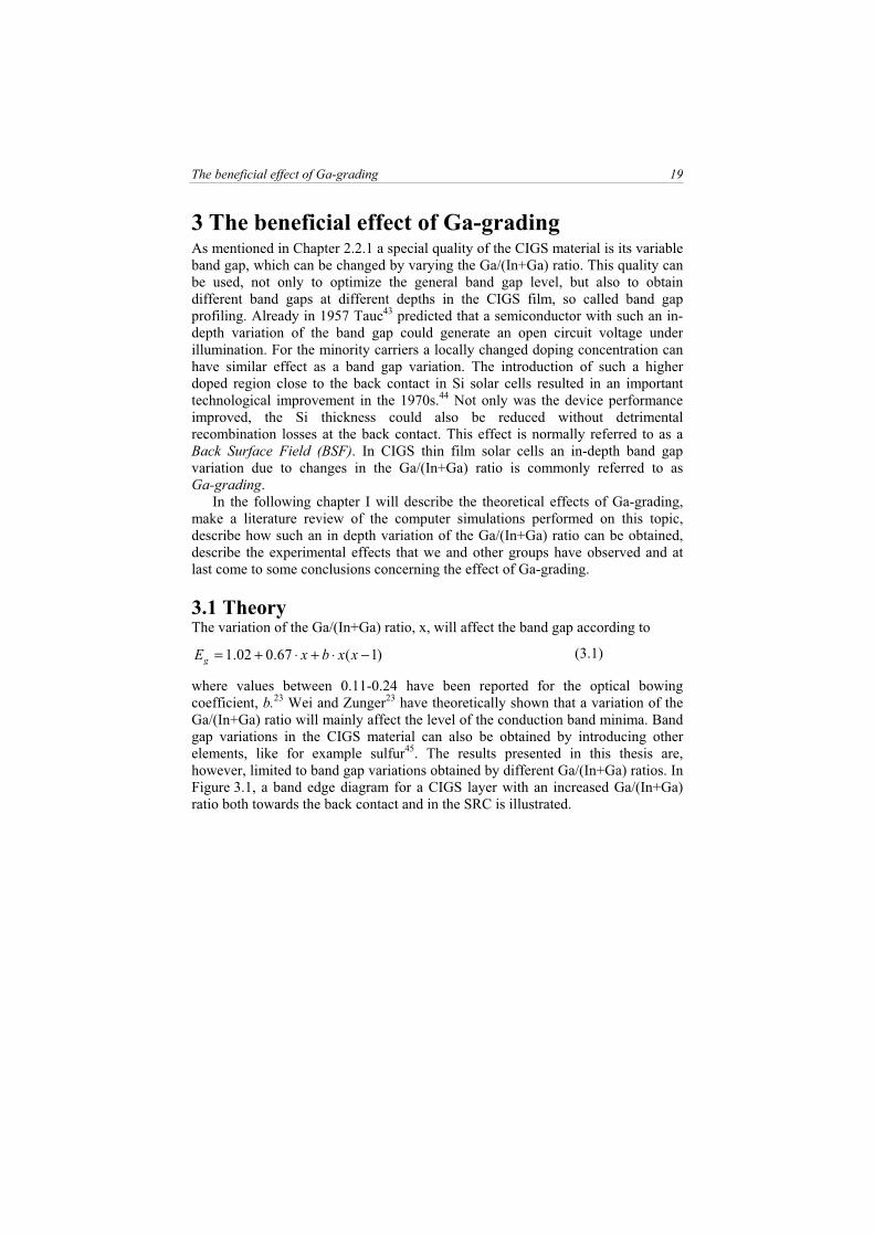
where values between 0.11-0.24 have been reported for the optical bowingcoefficient, b.23 Wei and Zunger23 have theoretically shown that a variation of theGa/(In+Ga) ratio will mainly affect the level of the conduction band minima. Band gap variations in the CIGS material can also be obtained by introducing otherelements, like for example sulfur45. The results presented in this thesis are, however, limited to band gap variations obtained by different Ga/(In+Ga) ratios. In Figure 3.1, a band edge diagram for a CIGS layer with an increased Ga/(In+Ga) ratio both towards the back contact and in the SRC is illustrated.

20 The beneficial effect of Ga-grading
Ecmin
EF
Evmax
∆Eg
O
FA e-
Figure 3.1. Band edge diagram of a CIGS thin film solar cell where the dotted line
illustrates how the conduction band minimum (Ecmin) is changed for a CIGS layer with an
increased Ga/(In+Ga) ratio towards the back contact and in the SCR. An additional force,
FA, acting on photogenerated electrons is obtained due to the band gap variation.
The locally increased band gap has two effects on the photgenerated electrons.First of all the recombination probability will be reduced at the position of the bandgap increase.46 Secondly an additional force, FA, acting on the these electrons is obtained and can be described by34
)(dx
nd
n
kT
dx
EdqF
g
A
∆⋅∆
+∆
= (3.2)
where ∆n is the change in electron concentration due to the Ga-grading. Here wehave assumed that d∆Nc/dx is zero, where ∆Nc is the change in density of states inthe conduction band due to the Ga-grading. The second tern in Equation 3.2 is a diffusion term, arising from a changed gradient of the electron concentration due tothe Ga/(In+Ga) variation. By assuming a linear variation of ∆Eg over a distance ∆xand a linear variation of ∆n over the same distance, we can see that this termbecomes small compared to the first term if ∆Eg>kT. In such a case the additional force from the Ga-grading becomes q·d∆Eg/dx. This force corresponds to an additional effective electric field, A =d∆Eg/dx.
3.1.1 Potential effects of Ga-grading
In the following I have classified the effects an in-depth variation the Ga/(In+Ga)ratio can have on the device performance into four different categories.
1) Improved Voc by reduced impact of regions with high recombination
At open circuit conditions the dominating part of the recombination isexpected to occur in the SCR region, c.f. Chapter 2.3.2. By increasing the Ga/(In+Ga) ratio here this recombination can be reduced, resulting in animproved Voc. But as illustrated in Figure 3.1, an increased conduction bandminimum in the SCR will also reduce the resulting electric field at the p-njunction with the possible consequence of a decreased carrier collection. Anincreased band gap in the front part will also reduce the absorption in thisregion. This can be compensated for by an increased absorption further into
The beneficial effect of Ga-grading 21
the CIGS layer, where the band gap not is increased. Photoelectrons generateddeeper into the CIGS material will on the other hand have a lower collectionprobability. Whether an increased Ga/(In+Ga) ratio in the SCR will have a netbeneficial effect or not is difficult to predict analytically.
At the CIGS/Mo interface it would be desirable with an additional force keeping the photoelectrons away from this interface, which is expected have a relatively high recombination velocity. By an increased conduction band minimum, towards the back contact, we can keep the good conductivity for themajority holes and at the same time reject the minority electrons. An increased band gap will also here, further into the CIGS layer, lead to a reduced lightabsorption. But since the photogeneration of carriers is expected to be rathersmall here anyway, this should only have a small effect on the resulting shortcircuit current. Whether this passivation of the CIGS back contact will haveany significant beneficial effect or not, will depend on how detrimental thisCIGS/Mo interface is for the device performance. As mentioned earlier a thinlayer of MoSe2 has been observed between the CIGS and Mo layer, whichpotentially could lead to a spontaneous passivation of the backcontact11. If thisis the case, the effect of an additional passivation by a Ga-grading would bereduced.
In order to analytically estimate the potential for a Voc improvement by a back contact passivation, Equations 3.3 and 3.4 can be used. Equation 3.3 describes the limitation of the Voc due to recombination in the neutral bulk,where the effective diffusion length is described by Equation 3.4.11
)ln(effAsc
VCeg
OCLNJ
NNqD
q
kT
q
EV −= (3.3)
)/cosh(/)/sinh(
)/sinh(/)/cosh(
dedbd
dedbddeff
LdDLSLd
LdDLSLdLL
++= (3.4)
Here Ld is the bulk diffusion length, De is the diffusion constant for minorityelectrons, Sb is the recombination velocity at the back contact, Nc and Nv thedensity of states in the conduction and valence band respectively, NA the netacceptor concentration and d is the thickness of the neutral bulk. With values of the parameters according to Rau and Schock11: De=2.6 cm2s-1, NC=6.7·1017
cm-3, NV=1.5·1019 cm-3 and NA=1016 cm-3 and assuming a Ld=1 µm and a SCRwidth of 0.3 µm, the gain in Voc by reducing Sb from 106 cm/s down to104 cm/s for a device with a standard CIGS thickness of 1.5 µm, is only 6 mV.This clearly illustrates that the bulk diffusion length must be at least as long as the CIGS thickness if the back contact should have any significant influenceon the device performance. For a device with a CIGS thickness of 0.5 µm, thecorresponding gain is 40 mV.
2) Improved Jsc due to field assisted carrier collectionCarrier collection of photoelectrons generated outside the SCR inhomogeneous CIGS layers rely on diffusion. The collection probability, fc,outside the SCR is given by38

22 The beneficial effect of Ga-grading
dL
X
C ef
−
= (3.5)
where x is the distance from the SCR and Ld is the diffusion length. As illustrated in Figure 3.1 an additional force acting on the electrons can beobtained by increasing the Ga/(In+Ga) ratio towards the back contact,potentially improving the carrier collection. In order to qualitatively estimatehow large influence a Ga-gradient can have on the carrier collection, we can estimate how far an electron can drift in the additional effective electric field during one minority carrier lifetime. Equation 3.6 describes the additionallength, L, that an electron with mobility, µe can drift in the additional effectiveelectric field A, during a lifetime, e .
[mLLqkT
L ddA
eAe
272 101/
⋅⋅≈⋅=⋅⋅= ]ξτξµ (3.6)
By the use of Ld = (De· e)1/2 and De=kT/q·µe we come to the second expression
in Equation 3.6. Assuming a linear additional effective electric field of 3·105 V/m through the neutral bulk of the CIGS layer (corresponding to aconduction band minimum increase of 0.3 eV over 1 µm) the last expression isobtained. For a typical diffusion length of 1 µm the additional length anelectron in this electric field can move is in average 10 µm. This means that the carrier collection can be significantly improved with the additional fieldobtained from Ga-grading. From Equation 3.6 we can also see that the lengthan electron can move in an electric field is proportional to Ld
2. This means that the additional length L becomes much longer in a material that has a longdiffusion length already without Ga-grading. On the other hand, the carriercollection in such a material is expected to be high anyway, and the potentialfor improvement is smaller than in a material with shorter diffusion length.Ultimately, it will be a balance between an improved carrier collection andreduced absorption that decides whether there will be a net improvement ofthe short circuit current or not, c.f. Equation 2.2.
3) Additional contribution to the Photovoltaic effect
As mentioned above, Tauc already in 1957 predicted that a semiconductorwith a band gap variation can generate an open circuit voltage under illumination. In the same way that an electric field, obtained at a p-n junction,can generate a Voc, an effective electric field originating from a compositionalvariation can generate a photovoltage. In 1979 Fonash and Ashok47 showed that these two effects can be added so that an additional photovoltaic effect isobtained from a band gap variation. However, unless the light intensity is highat the position where the band gap variation takes place, this additional effectwill not have a measurable contribution to the Voc.
4) Material quality effect Ga-grading can also indirectly influence the device performance by affecting the material quality of the CIGS layer. The lattice constants for CGS are somewhat different from those of CIS. This means that by introducingvariations of Ga/(In+Ga) ratio in the absorber, there will be stress built into the

The beneficial effect of Ga-grading 23
lattice and/or dislocations will occur. Both of these might have a detrimentalaffect on the material quality, lowering the minority carrier lifetime. If a CIGS layer is fabricated by co-evaporation and an increased Ga/(In+Ga) ratio towards the back contact is desired, the deposition must be started with pure CGS or CIGS with a high Ga/(In+Ga) ratio. Such layers with high Ga/(In+Ga)ratio have, to our experience, both smaller grains and a different preferred crystal orientation than CIGS with a lower Ga/(In+Ga) ratio.42 Since these layers are deposited in the beginning of the deposition they can affect theorientation and morphology of the complete CIGS layer.48 The electric qualityof CIGS layers with a Ga/(In+Ga) ratio above 0.5 is also reported to bereduced.49
3.1.2 Device simulations
The band gap profiling is commonly classified in two categories, normal and double grading. Normal grading is an increase of the band gap towards the backcontact, while the double grading profile has a minimum band gap some distanceinto the CIGS layer and an increased band gap both towards the back and frontcontact (see Figure 3.1). The complexity of how the device performance is affected by an in-depth variation of the Ga/(In+Ga) ratio is well illustrated by the diverseresults obtained by simulations on this topic.
A few device simulations have been performed using the simulation programADEPT50. Gray and Lee51 used this program and simulated a band gap structurewith a minimum band gap 0.5 µm into the CIGS layer. By linearly increasing theband gap from 1.0 at this point up to 1.2 eV at the back contact a smallimprovement of the carrier collection resulting in an increased Jsc of 0.6 mA/cm2
was obtained. A larger improvement of the device performance was obtained byincreasing the band gap towards the surface, which resulted in an increased Voc.Similar results were obtained by Gabor et al.32, using the same simulation tool.
Dhingra et al.52 used a p-i-n model for the CIS device structure and varied thegrading in the intrinsic region. With this structure improved efficiencies wereobtained using a normal, a double and a reverse (linearly increased band gap fromthe back to the front contact) grading structure. Topic et al.53 used a simulation tooldeveloped at the University of Ljubljana. In their optimum band gap profile theconduction band minimum increased linearly from just outside the SCR towardsthe back contact with 0.3 eV. Due to an increased Jsc this band gap structureimproved device performance by 5 %. By simulating a double grading profile, aslight increase in Voc was obtained, but due to a reduced FF and Jsc no gain inefficiency was observed. Menner et al.54 simulated a perfect electron mirror at the back contact and pointed out that the combination of a high absorption coefficientand short diffusion length (~ 0.7 µm) makes the gain by such a mirror insignificant.
In Paper III simulations were performed on how a normal Ga-grading profile could influence the device performance by reducing back contact recombination indevices with 2 µm thick CIS layers. In line with what was said under point 2 inChapter 3.1.1, a bulk diffusion length as long as 4 µm had to be assumed in order to explain the observed increase in Voc for the devices with Ga-grading.
All the simulations mentioned above predict a small increase of Jsc for a normalgrading profile, due to an improved carrier collection. A majority also predicts a larger gain in efficiency by the use of a double grading profile. In some cases
24 The beneficial effect of Ga-grading
different results are obtained, but since all the details of the simulations often notare presented, it is difficult to point out originating reasons for these differences.
3.2 Obtaining a Ga-gradient In the previous section we discussed a few effects of an in-depth variation of theGa/(In+Ga) ratio. The next question to be answered is - how can such an in-depthvariation of the Ga/(In+Ga) ratio be obtained and what are the limitations of theobtainable Ga/(In+Ga) profiles?
As described in Chapter 2.2.2, the selenization process results in a spontaneousnormal Ga-grading and in the three-stage process in a double Ga-grading profile.Some variation of these Ga-grading profiles is possible but the flexibility isstrongly limited.31, 45 By using a single or bilayer co-evaporation process, inprincipal any in-depth variation of the Ga/(In+Ga) ratio can be obtained by varyingthe gallium and indium deposition rates during the evaporation. The “as-deposited”Ga-grading profile is only limited by how fast the sources can change theirdeposition rate. However, as gallium and indium gradients are introduced into the material, diffusion will tend to reduce this Ga/(In+Ga) variation. Depending onhow fast this diffusion process is, it will limit the obtainable Ga-gradient profiles.In Paper VI and VII the indium and gallium diffusion and intermixing have beeninvestigated and a summary of the results and conclusions is presented in thefollowing.
3.2.1 Diffusion of In and Ga
A common belief in the CIGS community has been that the diffusion of galliumand indium is very rapid in Cu-rich CIGS films (Cu/(In+Ga) > 1). Because of this, a Cu-rich phase during deposition, has in some cases, been avoided under theassumption that no Ga-gradient would sustain such conditions. In our Ga-gradingexperiments, where we had a Cu-rich growth stage we did, however, still observe aGa-gradient. The Paper mostly referred to concerning the high diffusion in Cu-richgrown CIGS is by Walter and Schock48. In this Paper, multilayer structures of CISand CGS layers were evaporated on borosilicate glass (Corning®7059) substrates,resulting in essentially sodium-free CIS/CGS films. This motivated us toinvestigate how the presence of sodium influences the diffusion of indium and gallium. In order to do so, we fabricated two bilayer structures, CIS on CGS andCGS on CIS. The structures were both fabricated in a Cu-rich and in a Cu-poorprocess. In each CIS/CGS and CGS/CIS run, molybdenum coated soda lime glass substrates, with and without a sodium barrier of Al2O3 were used. This meant that we could study how the diffusion was influenced by sodium. The bilayers were deposited in 30 minutes at a substrate temperature of 500 ˚C, resulting in a totalthickness of 1 µm.. The bilayers were subsequently analyzed with secondary ionmass spectrometry, X-ray diffraction, scanning electron microscope andtransmission electron microscope equipped with energy dispersive x-rayspectroscopy (TEM-EDS). We made the following observations concerning thediffusion of indium and gallium:
• The main diffusion takes places inside the grains, possibly by vacancy diffusion, i.e. the diffusing atoms are moving via vacant lattice sites in the crystal. Diffusion in the grain boundaries is not significantly higher than

The beneficial effect of Ga-grading 25
inside the grains, not even if the layers are Cu-rich. Indium has a similardiffusivity in CGS as gallium in CIS.
• The diffusion is higher in sodium-free films than in films containingsodium, possibly due to increased concentration of metal vacancies, which could promote diffusion. Sodium free Cu-rich layers show higherdiffusion of In and Ga as compared to sodium-free Cu-poor layers. Thiscan be explained by higher concentrations of the for indium and galliumdiffusion more favorable VGa and VIn in the Cu-rich films compared to Vcu
in the Cu-poor films.55
• In the presence of sodium, there is no increase of the diffusion in Cu-richlayers as compared to Cu-poor layers.
From these bilayers structures we also got an estimation of how steep Ga-gradients that can be obtained in our CIGS layers. In Figure 3.2, SEM pictures,SIMS depth profiles and XRD plots are shown for two sodium containing bilayerstructures with CGS in the bottom and CIS at the top, one grown under Cu-richconditions (Cu/(In+Ga)=1.1) and one under Cu-poor conditions(Cu/(In+Ga)=0.95).
0
1 104
2 104
3 104
4 104
5 1040
100
200
300
400
500
600
7001 µm
1 µm
SEM SIMS XRD
0
1
2
3
4
5
0
100
200
300
400
500
600
700
103
103
103
103
103
26 26.4 26.8 27.2 27.60 0.2 0.4 0.6 0.8 1Ga/(Ga+In) 2θ (degrees)
28
CGSCIS
Figure 3.2. Two bilayers, CIS on top of CGS, grown with sodium under Cu-rich conditions
(top) and Cu-poor conditions (bottom) are illustrated with a SEM picture (left), SIMS
depth profile (middle) and XRD graph showing the (112) peak (right). The y-axis on the
SIMS profile is the sputter time, the dotted line in the SIMS profile represents the
measurement signal from the molybdenum back contact and the dotted lines in the XRD plot
indicate the peak position of the single CGS and CIS layers.
In the SEM pictures a two-layer structure can be seen, with smaller grains in the bottom part, where the CGS layer was deposited. The SIMS depth profiles andXRD plots show a relatively strong interdiffusion in both samples. The fastestvariation of the Ga/(In+Ga) ratio is seen in the Cu-poor layer, for which theGa/(In+Ga) ratio is ranging from around 0.8 to around 0.1 over a distance of0.5 µm. That results in an effective electric field about 106 V/m.

26 The beneficial effect of Ga-grading
In the XRD spectra, two separate peaks can be observed for both bilayerstructures. From both SIMS and XRD it seems as if the intermixing has been slightly higher close to the original interface between the CIS and CGS layer in the Cu-rich bilayer. In the SEM picture for this bilayer it can also be seen that the top part of the deposited CGS layer, closest to the original interface with the CIS layer, also has a larger grain size compared to the bottom part. We interpretate this as that a re-crystallization has occurred, see Paper VI. The re-crystallization could bea sign that some kind of re-organization has occurred, which could also possiblyexplain the enhanced intermixing of indium and gallium in this region. This re-crystallization effect is only observed in Cu-rich layers and is even stronger in thesodium free bilayers. The observation by Walter and Schock48 of a large difference in intermixing of In and Ga in Cu-rich and Cu-poor layers could be explained bythis effect, rather than an increased diffusion.
Concerning our initial question of how a Ga-gradient can be obtained and whatthe limitations are, we have learnt that:
• The interdiffusion is in general so high that depositing pure CGS inthe beginning of the process can be used to obtain a smooth Ga-gradient in the CIGS film.
• Ga-gradients can be nearly as steep in CIGS layers grown under Cu-rich conditions as CIGS layers grown under Cu-poor conditions.
• From Ga-grading an additional effective electric field of 106 V/m can be obtained. However, the stronger field, the larger change of theGa/(In+Ga) ratio, which also means a stronger material related effectas discussed in Chapter 3.1.1- point 4.
3.3 Experimentally observed effects of Ga-grading The CIGS layer in the world record device was fabricated with the three-stage
process9. As mentioned in the previous chapter, CIGS layers grown with thisprocess will have a double grading profile. But, since homogenous CIGS layers can not easily be fabricated with this process, it is difficult to make comparativestudies, showing that the high efficiencies obtained really are due to the double Ga-profile and not the process itself. In this perspective a single or bilayer co-evaporation process is a more suitable deposition method, since both homogenousand Ga-graded CIGS layers can be fabricated under similar conditions. In the following a review of experimentally observed effects of Ga-grading found in theliterature will be presented, thereafter our results on the effect of Ga-grading, at different conditions, will be described.
3.3.1 Literature review
The first paper describing an in-depth variation of the Ga/(In+Ga) ratio, in CISbased thin film solar cells, is a paper by Tuttle et al.56 (1989). In this paper CuGaSe2 layers of various thickness were deposited, both at the back and in thefront of CIS layers. With the CGS layer at the back the authors observed improvedQE values at long wavelengths but at the same time reduced values at shortwavelengths, with no resulting net gain in the Jsc. For the devices with CGSdeposited at the front a higher Voc was obtained, but an even stronger reduction of Jsc. Birkmire et al. 1990 increased the band gap towards the surface in CIS based solar cells by adding Ga. A slightly improved Voc was obtained but the overall
The beneficial effect of Ga-grading 27
efficiency was significantly reduced. Menner et al.54 in 1991 added differentlythick CIGS layers in the front part of CIS layers. The best device was obtained for a 20 nm thick Ga containing layer at the surface, which, however, was not significantly better than the pure CIS devices. In 1993 Jensen et al.57 fabricated CIS layers in a selenization process on substrates with and without a thin layer of aGa containing precursor and observed an efficiency increase from 10.5 to 11.7 %for the device with a Ga-precursor. The increased performance was mainly due to a gain in Voc (around 50 mV).
Contreras et al. 58 obtained in 1993 the so far highest open circuit voltage in a CIGS based solar cell, 687 mV, by the use of a Ga-graded co-evaporated CIGSlayer. Since no comparative study between samples with and without Ga-gradingwas performed, no conclusion can be made that the high Voc obtained was due tothe effect of the Ga-grading. In 1996 Contreras et al.59 compared results fromdevices with both normal and double grading profiles fabricated by both a bilayerand a three-stage co-evaporation process. For a similar Ga-profile the CIGS layersfabricated with the three-stage process yielded around 1 % unit higher efficienciesthan CIGS layers fabricated in the bilayer process. For the CIGS layers fabricated in the bilayer process, the ones with a double grading profile had slightly higherefficiencies than the CIGS layers with a normal grading profile. However, noconclusions concerning the beneficial effect of Ga-grading were made.
Gabor et al.31 investigated Ga-grading effects in devices where the CIGS layer is grown with the three-stage process. Different Ga/(In+Ga) ratios of the materialdeposited in the third stage were used and an increased efficiency was observed for increased Ga/(In+Ga) ratios. However, the gain was not due to an improved Voc as the simulations in the same paper predicted, but due to a higher FF and Jsc.
Shafarman et al.49 coevaporated CIGS layers with different bulk Ga/(In+Ga) ratioson substrates with and without an elemental Ga layer deposited prior to the CIGSdeposition. An increased FF was observed at all Ga/(In+Ga) ratios but a netreduction of the efficiency was obtained due to a reduced Jsc.
Dullweber et al.60 investigated samples with both normal and reverse Ga-gradings and concluded that the carrier collection can be influenced by gradedband gaps. Since the efficiencies were rather low (10-12 %), the Cu content variedlargely (between 17 and 22 atomic %) and an improved carrier collection was obtained also for a device with a reverse Ga-grading, no conclusion concerning thebeneficial effect of Ga-grading can be made. In the same paper, samples with a “multi grading” profile were analyzed. These and some additional samples werealso further investigated and discussed in Dullweber et al.60, 61, 62. The multigradingCIGS layers have an increased band gap towards the back contact, a minimumband gap 0.5-1 µm from the surface, an increased band gap in the SCR and a slightly reduced band gap at the very surface. For these devices the authors claimthat the Voc is correlated to the band gap in the SCR, whereas the Jsc is morecorrelated with the minimum band gap. The conclusions are not convincing and from the presented data it is not clear how the FF is influenced by the increased Ga/(In+Ga) ratio in the SCR.
In 2002 Orgassa et al.63 investigated alternative back contact metals incomparison to the normally used molybdenum. On to these different back contactmetals, both homogeneous and a Ga-graded CIGS layers were deposited. For devices with a homogeneous CIGS layer that experienced a significantly reduced

28 The beneficial effect of Ga-grading
device performance due to the back contact material, the authors observed a large improvement by the use of Ga-graded CIGS layers. However, the Ga-graded CIGS layers were 1.4 µm thick, while the homogeneous CIGS layer was only 0.9 µmthick. This makes the results less conclusive.
From the experimental results available in the literature no clear conclusionsconcerning the beneficial effect of the Ga-grading can be made, often because good reference devices with a homogenous CIGS layer are missing. It is, however,clear that high efficiency devices can be made using Ga-graded CIGS layers, bothwith normal and double grading profiles. The only cases for which a significantgain in efficiency is obtained by the incorporation of Ga, is for pure CIS 57.
3.3.2 Optimization of the Ga-profile
The aim of this study was to investigate if we could observe any beneficial effectof Ga-grading in our baseline devices, and if so, what the optimal Ga-profileshould look like. Most of the results are presented in Paper II, but our setup for measuring QE has been improved since Paper II was written and in this chapter there-measured data will be used. We limited our investigation to normal Ga-gradingprofiles, with an increased Ga concentration towards the back contact. The motivation for this limitation is the result from an earlier study in our group,mentioned in Paper II, where the Ga/(In+Ga) ratio was increased in the front partof the CIGS layer without any beneficial effect.
In Chapter 3.2 I concluded that a smooth Ga-gradient can be obtained bydepositing pure CuGaSe2 in the beginning of the process. By varying the thicknessof this initial CGS layer and also by varying the bulk Ga/(In+Ga) ratio, CIGSlayers with different Ga-grading profiles were obtained. In Figure 3.3 theevaporation rate profiles for a CIGS layer with a CGS layer deposited in thebeginning of the process is shown. Indium is replaced by gallium, here in the four first cycles of the deposition, otherwise the same evaporation rate profiles are usedas for our baseline process. From now on this process will be referred to as a Ga-graded baseline process.
0
0.2
0.4
0.6
0.8
1
Eva
pora
tion
rate
[a.u
.]
Ga
In
Cu
0 20 40 60Evaporation time [min]
Shutteropens
Figure 3.3. Metal evaporation profiles for a Ga-graded baseline evaporation. Ga replaces
In in the first four cycles.

The beneficial effect of Ga-grading 29
In order to investigate the Ga-grading profiles, obtained by the different CGSthicknesses and the different Ga/(In+Ga) bulk ratios, the CIGS layers were analyzed with SIMS and XRD. In Figure 3.4 (a) SIMS depth profiles of the Ga intensity (normalized to the intensities of the other elements) for five CIGS layers are shown and in Figure 3.4 (b) XRD plots of the (112) peak for the same CIGSlayers are shown. Two of the CIGS layers have a homogenous Ga/(In+Ga)concentration of 0.25 and 0.5 respectively. Two have the same bulk Ga/(In+Ga)concentrations but with a CGS layer deposited at the bottom, corresponding to30 % of the final thickness. The fifth CIGS layer has a bulk Ga/(In+Ga)concentration of around 35 % with a deposited CGS layer corresponding to around15 % of the total CIGS thickness, i.e. with a bulk Ga/(In+Ga) ratio in between thetwo others and with half of the CGS thickness.
00 0.5 1 1.5 2
Depth [µm]
Nor
mal
ized
Ga
conc
entr
atio
n [a
.u.]
0.25
0.5
0.75
1
Low Ga , No CGS
High Ga , thick CGS
Low Ga, thick CGS
Medium Gathin CGS
0
2 10 5
4 10 5
6 10 5
8 10 5
1 10 6
1.2 10 6
0
5 10 4
1 10 5
1.5 105
2 10 5
26.6 26.8 27 27.2 27.4 27.6 27.8
High Ga , no CGS
Low Ga , No CGS
Medium Gathin CGS
High Ga , thick CGS
Low Ga, thick CGS
XR
D in
ten
sity
[cp
s] X
RD
inte
ns
ity[cp
s]
Diffraction angle (2θ) [degrees]
High Ga , no CGS
Figure 3.4. a) SIMS depth profiles of the normalized Ga intensity and b) XRD plot of the
(112) peak for five CIGS layers with different Ga/(In+Ga) ratios and CGS back contacts.
The SIMS depth profiles and the XRD data together give a coherent picture ofthe different Ga-grading profiles. From the SIMS profile we get the depth profileand from the XRD spectra we can estimate the maximum and minimumGa/(In+Ga) ratios. As expected the strongest Ga-gradient is obtained for the Ga-graded CIGS layer with the lowest Ga/(In+Ga) bulk ratio (0.25) and the thicker

30 The beneficial effect of Ga-grading
CGS layer, corresponding to 30 % of the total thickness. In this film the Gaconcentration changes throughout the entire CIGS layer with a Ga/(In+Ga) ratio ofaround 0.8 at the back and slightly above 0.25 at the front, according to the XRD peak positions. The Ga-gradient in the layer with the highest Ga concentration, as well as the CIGS layer with the medium high Ga concentration, does not reach all the way to the front surface. The upper third part of these CIGS layers has a constant Ga concentration.
The CGS bottom layer also has an impact on the film texture. By comparingCIGS films with and without a CGS bottom layer, we observe a much lowerpreferred (112) orientation in the films with a CGS layer. Thicker CGS bottomlayers lead to a further reduction of the (112) orientation.
In Figure 3.5 the I-V data for these five samples is shown as a function of thethickness of the initial CGS layers and their bulk Ga/(In+Ga) ratio.
Ga/(In+Ga) [%]
CG
S la
yer
thic
knes
s [%
]
25 50
0
30
15
η: 15.3 FF:75.3
Jsc:31.2 Voc:652
: 15.2 FF: 77
Jsc:27.8 Voc: 710
η: 14.8 FF: 77.7
Jsc: 31.7 Voc: 600
η: 16.4 FF: 76.8
Jsc: 30.3 Voc: 706
η:15.6 FF: 76.7
Jsc:26.9 Voc: 752
37
Figure 3.5. η, FF, Jsc, and Voc for five devices with different bulk Ga/(In+Ga) ratios and/or
different thickness of the bottom CGS layer(given in % of the total thickness).
The trend for these devices is an increased performance as Ga-graded CIGS layers are used. The best efficiency is obtained for the sample with a bulkGa/(In+Ga) ratio of around 35 % combined with a CGS layer corresponding toaround 15 % of the total CIGS thickness. This recipe was also used in thefabrication of the current world record thin film solar module, with an efficiency of 16.6 %10. From the I-V parameters in Figure 3.5 it appears like the Voc is improvedfor the devices with a Ga-graded CIGS layer. However, as can be seen in Figure 3.4, the Ga-graded CIGS layers have slightly increased Ga concentrations also in the front part, which means that the minimum band gap is increased. Fromthis data alone we cannot say whether the increase in Voc is due to this increasedband gap or due to the Ga-grading. Since the Cu/(In+Ga) ratio varies somewhat for these CIGS layers (between 0.8 and 0.95), and this variation can have some effecton the device performance we save the detailed analysis of the beneficial effect of Ga-grading for the next chapter. Concerning the Ga-grading optimization it seems

The beneficial effect of Ga-grading 31
as if a CGS layer corresponding to around 15 % of the total thickness results in a superior Ga-grading profile compared to a CGS layer that corresponds to 30 % ofthe total thickness.
3.3.3 The effect of Ga-grading at baseline conditions
Since the effect of Ga-grading seems to be relatively small we have compared alarge set of devices with and without a Ga-grading in this study, so that a statistically significant result can be obtained. The results are from Paper VIII, withsome new unpublished data added.
Both the baseline process and the Ga-graded baseline process are regularly used to fabricate CIGS layers in our laboratory. In the Ga-graded baseline process aCGS layer with a thickness corresponding to 10-15 % of the total thickness is used.Since the device performance is significantly affected by the Cu/(In+Ga) ratio, see for example Paper VIII, and the effect of Ga-grading is relatively small, it onlymakes sense to compare devices with a similar Cu/(In+Ga) ratio. In order to compare open circuit voltages (Voc) and short circuit currents (Jsc) of devices withslightly different Ga/(In+Ga) ratios, we introduce the following “band gapnormalized” I-V parameters: ∆Voc = Voc-(Eg/q-0.6V) and Jsc
rel = Jscmeasured/Jsc
max.Here Eg is the band gap of the CIGS layer, q the elementary charge, Jsc
measured is theJsc obtained from the QE measurement and Jsc
max is the Jsc that would be obtained ina device with the QE equal to 1 between 360 nm and the wavelength correspondingto the band gap, Eg. For example is Jsc
max 40 mA/cm2 for a band gap of around1.2 eV, which means that 1 % unit of Jsc
rel corresponds to 0.4 mA/cm2. The expression for ∆Voc is defined as above since the Voc is roughly proportional to Eg
for band gaps between 1.1 and 1.25 eV37 and by subtracting 0.6 V, ∆Voc valuesgreater than zero are generally obtained.
In Figure 3.6 the η, ∆Voc, Jscrel and the FF is shown as a function of the
Cu/(In+Ga) ratio for a large number of samples, grown at baseline conditions bothwith and without a Ga-grading. I remind that each point in Figure 3.6 is an average over 8 individual cells.
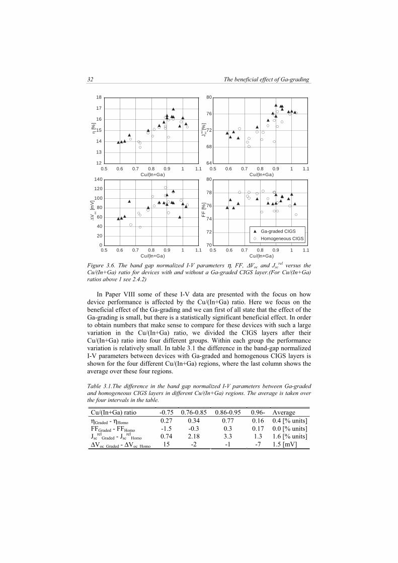
32 The beneficial effect of Ga-grading
0
20
40
60
80
100
120
140
0.5 0.6 0.7 0.8 0.9 1 1.1
Vo
c [mV
]
Cu/(In+Ga)
64
68
72
76
80
0.5 0.6 0.7 0.8 0.9 1 1.1
J scre
l [%]
Cu/(In+Ga)
12
13
14
15
16
17
18
0.5 0.6 0.7 0.8 0.9 1 1.1
[%]
Cu/(In+Ga)
70
72
74
76
78
80
0.5 0.6 0.7 0.8 0.9 1 1.1
FF
[%]
Cu/(In+Ga)
Ga-graded CIGS
Homogeneous CIGS
Figure 3.6. The band gap normalized I-V parameters η, FF, ∆Voc and Jscrel versus the
Cu/(In+Ga) ratio for devices with and without a Ga-graded CIGS layer.(For Cu/(In+Ga)
ratios above 1 see 2.4.2)
In Paper VIII some of these I-V data are presented with the focus on how device performance is affected by the Cu/(In+Ga) ratio. Here we focus on the beneficial effect of the Ga-grading and we can first of all state that the effect of theGa-grading is small, but there is a statistically significant beneficial effect. In order to obtain numbers that make sense to compare for these devices with such a large variation in the Cu/(In+Ga) ratio, we divided the CIGS layers after theirCu/(In+Ga) ratio into four different groups. Within each group the performancevariation is relatively small. In table 3.1 the difference in the band-gap normalizedI-V parameters between devices with Ga-graded and homogenous CIGS layers isshown for the four different Cu/(In+Ga) regions, where the last column shows theaverage over these four regions.
Table 3.1.The difference in the band gap normalized I-V parameters between Ga-graded
and homogeneous CIGS layers in different Cu/(In+Ga) regions. The average is taken over
the four intervals in the table.
Cu/(In+Ga) ratio -0.75 0.76-0.85 0.86-0.95 0.96- AverageηGraded - ηHomo 0.27 0.34 0.77 0.16 0.4 [% units]FFGraded - FFHomo -1.5 -0.3 0.3 0.17 0.0 [% units]Jsc
relGraded - Jsc
relHomo 0.74 2.18 3.3 1.3 1.6 [% units]
∆Voc_Graded - ∆Voc_Homo 15 -2 -1 -7 1.5 [mV]

The beneficial effect of Ga-grading 33
In average the devices with a Ga-graded CIGS layer have 0.4 % units higherefficiency than devices with a homogeneous CIGS layer with a similar Cu/(In+Ga)ratio. The gain is largest for Cu/(In+Ga) ratios between 0.86-0.95, where also theoverall best device performance is obtained. All the gain in efficiency can be attributed to an improved Jsc. Concerning the FF, there is no gain for devices with aGa-grading and at Cu/(In+Ga) ratios below 0.9 the FF is even slightly larger for thedevices with homogenous CIGS layers. The difference in Voc (same as the difference in ∆Voc) is very small. In Figure 3.7, the QE as a function of wavelengthis shown for two typical devices, with and without Ga-grading.
0
0.2
0.4
0.6
0.8
1
400 600 800 1000 1200
QE
Wavelength [nm]]
HomogeneousCIGS
Ga-gradedCIGS
Figure 3.7. QE for devices with and without Ga-grading but similar Cu/(In+Ga) ratio.
The carrier collection for the device with the Ga-graded CIGS layer is improved for photoelectrons generated by light with a wavelength longer than 800 nm. The improved carrier collection in Figure 3.6 corresponds to a gain in Jsc of 0.7 mA/cm2. In Paper VIII we argue that the longest diffusion length is obtained forthe material with a Cu/(In+Ga) ratio between 0.85 and 0.95 and it is also for thesedevices that we see the largest gain in Jsc due to the Ga-grading.
3.3.4 The effect of Ga-grading at high deposition rates
In this chapter the effect of Ga-grading is investigated for devices where the CIGS layer is deposited at a higher deposition rate than under baseline conditions, is investigated. Both in Paper VI and Paper VIII CIGS layers at high depositions rates, with and without Ga-grading, are presented. However, the Ga-graded CIGSlayers presented in Paper VI, have a more optimized Cu/(In+Ga) ratio, compared to the homogenous CIGS layers. This means that they are less suitable for a detailedanalysis of the beneficial effect of Ga-grading. Most of the results presented hereare from Paper VIII.
In order to reduce the deposition times, we simulated an increased travel speed of the substrates and increased the evaporation rates correspondingly so that thesame CIGS thicknesses were obtained. No effect of the Ga-grading profile due tothe increased deposition rates was observed. In Figure 3.8 we compare the band gap normalized I-V parameters as a function of the Cu/(In+Ga) ratio for deviceswith and without Ga-grading, where the CIGS layers is grown at 15 minutes.

34 The beneficial effect of Ga-grading
64
66
68
70
72
74
J scre
l [%]
0.7 0.75 0.8 0.85 0.9 0.95 1Cu/(In+Ga)
0.65 1.05
70
71
72
73
74
75
76
77
FF
[%]
0.7 0.75 0.8 0.85 0.9 0.95 1Cu/(In+Ga)
0.65 1.05
20
40
60
80
100
120
140
V oc [m
V]
0.7 0.75 0.8 0.85 0.9 0.95 1Cu/(In+Ga)
0.65 1.05
12
12.5
13
13.5
14
14.5
15
15.5
[%]
0.7 0.75 0.8 0.85 0.9 0.95 1Cu/(In+Ga)
0.65 1.05
Ga-graded CIGS
Homogeneous CIGS
Figure 3.8. The η, FF, ∆Voc and Jscrel as a function of the Cu/(In+Ga) ratio for devices with
and without a Ga-graded CIGS layer fabricated at 15 minutes.
Also for these devices, where the CIGS layers are grown at four times higherevaporation rate than used in the baseline process, a beneficial effect of the Ga-grading is observed. In order to obtain numbers for comparison for these devices itis enough to divide them into two different categories since they are less influencedby the Cu/(In+Ga) ratio. In Table 3.2 the differences in the band gap normalizedI-V parameters between devices with and without a Ga-graded CIGS layer are shown.
Table 3.2. The differences in band gap normalized I-V parameters between Ga-graded and
homogeneous CIGS layers in different Cu/(In+Ga) regions. The average is the mean value
of the two intervals in the table.
Cu/(In+Ga) ratio -0.80 0.81- AverageηGraded - ηHomo 0.5 0.3 0.4 [% units]FFgraded - FFhomo 1.4 0 0.7 [% units]Jsc
relgraded - Jsc
relhomo 2.0 0.5 1.3 [% units]
∆Voc (graded) - ∆Voc (homo) -2 11 4 [mV]
As can be seen from Table 3.2 the average gain in efficiency is 0.4 % units, which is the same as for the devices with the CIGS layers grown at 60 minutes.Also at this shorter deposition time the dominant gain is seen in the Jsc, althoughsome gain also is obtained in the FF. The largest gain in Jsc is seen for Cu/(In+Ga) ratios below 0.80, in contradiction to the previous section, where the larger gain

The beneficial effect of Ga-grading 35
was obtained for higher Cu/(In+Ga) ratios. As discussed in Paper VIII, there is some additional loss mechanisms introduced at higher Cu/(In+Ga) ratios for thesedevices, which for example results in a wavelength independent reduction of theQE. These additional losses might overshadow some of the effects of Ga-grading.
3.3.5 The effect of Ga-grading for CIS
In Paper III the influence of Ga-grading in pure CuInSe2 was investigated. CIS layers with a 0 to 1.25 µm thick CGS layer at the back were fabricated with constant evaporation rates under Cu-poor conditions. The total thickness was around 2 µm for all the layers. In the upper 250 nm a small amount of Ga was added, so that a Ga/(In+Ga) ratio of around 0.2 was obtained. No beneficial effectof this top layer could, however, be proven. In Figure 3.9a depth profiles of theGa/(In+Ga) ratio obtained from SIMS measurements are shown and in Figure 3.9babsorbtance data as a function of wavelength are shown for some of the CIS/CGSsamples.
0
0.2
0.4
0.6
0.8
1
0 0,5 1 1,5 2Depth m]
Ga
/(In
+G
a)
0
0.2
0.4
0.6
0.8
1
1.2
600 800 1000 1200 1400
pure CIS0 µm CGS0.25 µm CGS1. 0 µm CGS
Ab
so
rptio
n
Wavelength [nm]
Figure 3.9.(a) SIMS depth profiles and (b) absorbtance data (compensated for reflection
losses) as a function of wavelength for CIS layers with different thick CGS layers at the
back. “Pure CIS” means that this layer, in contrast to the others, does not have any Ga in
the front region.
In Figure 3.11a we can see that the CIS layer with a 1 µm thick CGS layerdeposited at the back, has a very steep gradient of the Ga/(In+Ga) ratio. In Figure3.11b it can also be seen that the absorbtance at long wavelengths is reduced forthis CIGS layer, which corresponds to a Jsc reduction of around 2 mA/cm2. The corresponding loss for the CIGS film with a 0.25 µm thick CGS layer at the back is around 0.5 mA/cm2. A small reduction in absorption, compared to the pure CISlayer, is also seen for the film with no CGS at the back, but only a 250 nm thicklayer of Cu(In0.8Ga0.2)Se2 at the front. The absorbtance data are obtained fromreflectance and transmittance measurements performed on the CIS/CGS layersdeposited on glass.
In Figure 3.10 the I-V parameters as a function of the CGS layer thickness are shown. These Jsc data are obtained from the I-V measurement and not from QE measurements, because QE measurements were not available for all the samples.

36 The beneficial effect of Ga-grading
8
9
10
11
12
13
14
15
0 0.2 0.4 0.6 0.8 1 1.2
[%]
CGS thickness [µm]
24
26
28
30
32
34
36
J sc [
mA
/cm
2 ]
0 0.2 0.4 0.6 0.8 1 1.2CGS thickness [µm]
66
68
70
72
74
76
FF
[%]
0 0.2 0.4 0.6 0.8 1 1.2CGS thickness [µm]
400
450
500
550
600
650
Voc
[mV
]
0 0.2 0.4 0.6 0.8 1 1.2CGS thickness [µm]
Figure 3.10. I-V parameters as a function of the CGS layer thickness at the back in devices
with CIS/CGS absorber layers.
By adding an only 0.13 µm thick CGS layer at the back an improved efficiencyof around 2 % units is obtained. The gain in efficiency is mainly due to anincreased Voc, which is around 60 mV higher for the device with a 0.25 µm thickCGS layer compared to the CIS layers without any CGS bottom layer. A smallgain of the short circuit current is also obtained for CGS layers up to 0.25 µm,despite the fact that the absorbtance is reduced. When the CGS thickness is increased above 0.5 µm the performance is reduced compared to the optimal value. This is mainly because the Jsc starts to decrease, in accordance with the absorbtance measurements. The FF shows no correlation with the added CGS layer.
3.3.6 The effect of Ga-grading at different CIGS thicknesses
In chapter 3.1.1, we predicted that the back contact passivation would have anincreased importance as the CIGS thickness was reduced. Possibly such apassivation can be obtainable by an increased Ga/(In+Ga) ratio towards theabsorber backside, By comparing devices with different CIGS thicknesses, withand without Ga-grading, we should find out whether the back contact isdetrimental for the device performance and if it is, whether a Ga-grading can helpor not. Most of the results in this chapter are presented in Paper IV.
CIGS layers were fabricated with a thickness ranging from 1.8 down to0.15 µm, both with and without Ga-grading. At the CIGS thickness of 0.5 µm we also performed an optimization of the Ga-gradient by trying CGS layers withdifferent thickness. Cu-poor baseline and Cu-poor Ga-graded baseline evaporationrate profiles were used (see Chapter 2), where only the deposition time wasshortened in order to obtain the thinner CIGS layers. The CGS thickness, in theGa-graded CIGS layers, was in this study corresponding to around 5-10 % of total

The beneficial effect of Ga-grading 37
thickness. In Figure 3.11 the band gap normalized I-V parameters η, ∆Voc, Jscrel and
FF are shown as a function of the CIGS thickness for devices with and without Ga-grading.
J scre
l[%
]
0
20
40
60
80
100
50
55
60
65
70
75
80F
F [%
]
0 0.25 0.5 0.75 1 1.25 1.5 1.75 2CIGS Thickness [µm]
0 0.25 0.5 0.75 1 1.25 1.5 1.75 2CIGS Thickness [µm]
0
2.5
5
7.5
10
12.5
15
17.5
[%]
0 0.25 0.5 0.75 1 1.25 1.5 1.75 2CIGS Thickness [µm]
Vo
c [mV
]
-20
0
20
40
60
80
100
120
0 0.25 0.5 0.75 1 1.25 1.5 1.75 2CIGS Thickness [µm]
Ga-graded CIGS
Homogeneous CIGS
Figure 3.11. The η, FF, ∆Voc and Jscrel versus absorber thickness for samples with (filled
triangles) and without (open circles) a Ga-graded CIGS layer
The general device performance as a function of the CIGS thickness will bediscussed in Chapter 4, while we focus here on the effect of Ga-grading. In Paper IV, we did not make any correction for the fact that the devices with thinner CIGSlayers in general had slightly higher band gaps. Here, this is done and theconclusions are slightly different. For devices with homogeneous CIGS layers theVoc is reduced by roughly 70 mV as the CIGS thickness is reduced from 1.8 µmdown to 0.5 µm. Around 20 mV of this loss can be attributed to the reduction in Jsc,which means that the loss due to an increased recombination is about 50 mV. Thecorresponding loss in Voc for devices with Ga-graded CIGS layers is only 20 mV.The gain in Voc by using a Ga-graded CIGS layer increases as the CIGS thicknessis reduced, from 10 mV at 1.8 µm to around 30 mV at 0.5 µm. A similar behavioris seen for the FF, which for devices without Ga-grading is reduced almost linearlyfrom 76 % down to below 70 %, as the CIGS thickness is reduced from 1.8 to0.5 µm. For the devices with a Ga-graded CIGS layer, however, the FF staysunaffected, around 75 %, as the CIGS thickness is decreased down to 0.5 µm.Concerning the Jsc no significant difference between devices with and with out Ga-grading was observed for these devices. The resulting gain in efficiency, due to theGa-grading, is thus increasing with a decreased CIGS thickness.

38 The beneficial effect of Ga-grading
In Figure 3.12 the ∆Voc and FF for devices with a 0.5 µm thick CIGS layer andan additional CGS layer at the back are shown as a function of the CGS layerthickness.
0 50 100 150 200
Vo
c[m
V]
CGS thickness [nm]
0
20
40
60
80
100
68
70
72
74
76
78F
F [%
]
Voc
FF
Figure 3.12. Voc and FF versus CGS bottom layer thickness for devices with a CIGS
thickness of 0.5 µm.
The 30 nm additional CGS layer corresponds to around 6 % of the totalabsorber thickness, which was the CGS thickness used for the devices in Figure3.11. By increasing the CGS thickness to 60 nm an additional gain in Voc of around 20 mV and in FF of close to 2 % units is obtained. From figure 3.13 we stated thatthe loss in Voc for the device with the 0,5 µm thick Ga-graded CIGS layer was around 20 mV compared to devices with standard thickness of the CIGS layers.This means that, after an optimization of the Ga-grading, devices with a 0.5 µmthick absorber layer can obtain Voc and FF as high as for standard devices. The gain compared to homogenous CIGS layers for this device is around 50 mV in Voc
and 8 % units in FF. Increasing the CGS thickness further, up to 160 nm, thedevice performance is slightly reduced again. This means that the Ga-grading profile used for the devices in Figure 3.11 was close to optimum but a slight furtherimprovement is obtained by increasing the CGS thickness to around 10-15 % of the CIGS thickness. No gain in Jsc correlated to the Ga-grading was observed for these devices.
3.5 Discussion and Conclusions For devices with 1.5-2 µm thick CIGS layers grown in a Ga-graded baselineprocess, the average gain in efficiency, compared to CIGS layers grown in a normal baseline process, is about 0.4 % units. The gain is due to an improved shortcircuit current (Jsc) which is increased due to an enhanced QE response atwavelengths above 800 nm. In average the improvement in Jsc is around 0.5 mA/cm2, which is in good agreement with the gain obtained in a number ofsimulations31, 50, 53. All these results indicate that the improved carrier collection isdue to the additional electric field obtained by the Ga-grading, as discussed inpoint 2 - Chapter 3.1.1. The fact that Voc and FF are not significantly influenced bythe Ga-gradient could be explained by that the recombination current, limiting

The beneficial effect of Ga-grading 39
these parameters, is strongly dominated by recombination in the SCR (c.f.Chapter 2.3).
A significantly larger beneficial effect of the Ga-grading is obtained for thinCIGS layers. The gain in efficiency due to the Ga-grading is increased as theabsorber thickness is reduced (at least for CIGS thickness down to 0.5 µm). Anincrease in both FF and Voc, which can be correlated to a reduced saturationcurrent, is the reason for the gain in efficiency. At a CIGS thickness of 0.5 µm theimprovement in efficiency, by using a Ga-graded CIGS layer, is around 2.5 % unitsand the obtained values of Voc and FF reach the same level as for devices withstandard thick CIGS layers. These observations are all in agreement with that theGa-grading passivates the back contact, which becomes increasingly detrimentalfor the device performance as the CIGS thickness is reduced. The theoreticallypredicted gain in Voc, from a reduced back contact recombination in point 1-Chapter 3.1.1 is also in agreement with the obtained results. Since we did notobserve any increased FF or Voc for devices with 1.5-2 µm thick Ga-graded CIGSlayers it indicates that the CIGS/Mo interface does not play a significant role inthese devices. For devices with thinner CIGS layers no improvement in Jsc, relatedto the Ga-grading was observed. This could be understood by that in thin CIGSlayers the relative absorption loss due to the Ga-grading is larger, and the need forfield assisted carrier collection is smaller than in absorber layers with standardthicknesses.
Devices with CIGS layers grown at an elevated deposition rate, exhibit asimilar gain in efficiency due to the Ga-grading as devices with CIGS layers grownat 60 minutes. Also here the main part of the gain is due to an improved Jsc, but a small gain in FF is also obtained.
We, as well as others, have observed a large beneficial effect of adding Ga inpure CIS layers. By adding only 0.13 µm CGS at the back of a 2 µm thick CISlayer, we obtained an around 2 % units gain in efficiency. The suggestedexplanation for this observation was in Paper III a reduced back contact recombination. Due to a number of reasons, we do not longer find this explanationvery probable. First of all this interpretation does not fit to the other observationsand conclusions made above. It also requires a bulk diffusion length of around 4 µm, which is longer than normally observed. We instead suggest that theintroduction of gallium itself is the main reason for the observed improvement in performance. In Wei et al.64 a number of beneficial effects obtained by introducinggallium in CIS are summarized. For example the introduction of gallium leads to a larger domain for stoichiometric CIGS ( -phase) in the phase diagram, potentiallyleading to a generally improved material quality. At our lab we have also observedan improved device performance for CIS layers by adding very smallhomogeneous amounts of Ga.
Concerning the optimal Ga-grading profile our results suggest that, independentof the CIGS thickness, deposition rate and composition, the optimal normal Ga-profile is obtained by starting the deposition with a CGS layer corresponding to 10-15 % of the total absorber thickness. Such a layer results in a Ga-gradient startingapproximately 1/3 into the CIGS layer and reaches a Ga/(In+Ga) ratio of around 0.7 at the back contact. By increasing the initial CGS thickness further a reduceddevice performance was obtained. This could be correlated both larger absorption

40 The beneficial effect of Ga-grading
related losses and to an increase in the potentially detrimental material relatedeffects mentioned in chapter 3.1.1- point 4.
In this work we have focused on the normal Ga-grading profile, and in theexperiments where we have used a double grading profile, no additional beneficial effect was observed. Despite the results from many simulations showing a superiordevice performance for a double grading profile compared to a normal grading,there are no clear experimental results showing this in the literature. As mentionedabove, the CIGS layer in the world record device has a double grading profile,which proves that high performance devices can be obtained with such a profile.But as shown by Contreras et al.59 the three-stage process results in around 1 %unit higher efficiency devices compared to devices where CIGS layers have a similar double graded profile, but grown in a single stage process. This indicatesthat it is the three-stage process in it self that is the origin of the high performanceand not necessarily the double Ga-grading profile.
Concerning the beneficial effect of Ga-grading we conclude:• For devices with a standard thick CIGS layer (1.5-2 µm) with a
Ga/(In+Ga) ratio between 0.25-0.5, a Cu/(In+Ga) ratio between 0.7 and 1 and a deposition time from 60 down to 15 minutes the efficiencygain with a normal Ga-grading profile is in the order of 0.5 % units.The main part of the gain is due to an improved carrier collection atlong wavelengths due to the additional effective electric field obtainedfrom the increased Ga/(In+Ga) ratio towards the back contact. No significant gain in Voc or FF related to the Ga-grading is obtainedunder these conditions.
• By reducing the CIGS thickness, the beneficial effect of Ga-grading isincreased. At an absorber thickness of 0.5 µm the gain in efficiency isaround 2.5 % units due to an increased FF and Voc, which becomescomparable to those obtained for standard devices. The increased gain at thinner CIGS layers is due to a passivation of the CIGS backcontact, which becomes increasingly detrimental for the deviceperformance as the CIGS thickness is reduced.
• No additional gain in performance due to an increased Ga/(In+Ga) ratio in the front part of the CIGS layer can be concluded.

Next generation CIGS layers 41
4 Next generation CIGS layers From an application point of view, the two most important numbers for a solar cellmodule are the module efficiency and the module production cost. Among the fivedifferent layers within the device structure, the CIGS film is the layer associatedwith the highest production cost. A large capital cost for the deposition equipment,in combination with a relatively long deposition time leads to the high productioncost for the CIGS layer. The need for lowering the production cost for the nextgeneration CIGS layers can be illustrated by the following example:In Figure 4.1 a sketch of a CIGS in-line deposition system is shown together withan equation for estimating the yearly production from this CIGS evaporator.
Deposition area
Deposition timeYearly production = Efficiency Yield "Up-time"oo
o
CIGS Evaporator
SeSe
Figure 4.1. Sketch of a CIGS in-line deposition system and an equation for estimating the
yearly production (in Wp) from such a system.
Standard values of these parameters today are: module efficiency= ~10 %, deposition area= ~1 m2, deposition time=30 min, up time=5700 h (three shiftoperation) and by assuming a yield of 100 % we end up with a yearly production ofabout 1 MWp. Assume that we would like to produce the complete modules for 1 $/W and that the production of the CIGS layer not may exceed 10 % of the total production cost. The yearly available money, for both capital and operational costsof the CIGS production then becomes around $ 100 000. Only the salaries for twofull time workers will cover this amount of money, clearly pointing out the need toeither develop a low-cost deposition equipment and/or increase the productionfrom an “expensive” deposition system.
Beside the deposition methods, described in Chapter 2 (co-evaporation and selenization), there are a number of alternative ways of depositing the CIGS layer.Electro-deposition is one example of a potentially cheaper method. CIGS filmsresulting in 10 % efficiency small area devices have been fabricated with thismethod65, but many things remains to be improved before this process can be scaled up and produce large, high efficiency modules at a lower cost. We will here instead focus on how we can increase the production from a co-evaporationsystem.
Among the parameters given in Figure 4.1, our estimate is that the deposition-time hosts the largest potential for improvement. Increasing the efficiency would be even more valuable, but the effort put into this is already very high and thepossibility for a substantial improvement is limited. Enlarging the deposition areashould be possible, but this will also make the deposition system more expensive.

42 Next generation CIGS layers
This motivated us to investigate the potential for reducing the deposition time ofthe CIGS layer as a fundamental parameter for lowering the cost. The depositiontime is determined by the final thickness of the CIGS layer and the deposition rateused during deposition, according to Equation 4.2:
rateDeposition
thicknessCIGStimeDeposition = (4.2)
In the following we will show that by decreasing the CIGS thickness andraising the deposition rate it is possible to increase the yearly production, from theCIGS deposition system in Figure 4.1 by up to 30 times, with only a marginallyreduced module efficiency.
4.1 Reduced CIGS thicknessDecreasing the thickness of the CIGS layer leads, in addition to a reduceddeposition time, to a lower material consumption. A reduction of material usage isparticularly important for indium and gallium since the supply of these metalsmight become an issue if CIGS thin film solar cells will be produced in very large volumes (~70 GWp/year).66 In the following we discuss the effects on the deviceperformance when the CIGS thickness is reduced, and the possibilities to improvethe performance for devices with thin CIGS layers. Most of the results arepresented in Papers IV and IX.
4.1.1 Performance as a function of CIGS thickness
The standard thickness of the Cu(In,Ga)Se2 layer used in the industry is around2 µm67, 68. A reduction of this absorber thickness has advantages as mentionedabove, however, it is also associated with a number of problems:
• Reduced absorption: Although the absorption coefficient is high for theCIGS material, a decreased thickness will reduce the absorption andthereby also the Jsc.
• Increased risk for shunting: In a previous study by T. Negami et al.69 an increased shunting was observed as the CIGS thickness was reduced down to around 0.5 µm, which resulted in strongly decreased performance.
• Increased influence of the back contact: As the CIGS thickness is reduced, the risk for back contact recombination increases.
• Reduced long-term durability: Possibly a thinner CIGS layer will reducethe lifetime of the solar cell. This could for example happen if thecorrosion of the CIGS layer itself is critical for the solar cell lifetime.
• Reduced material quality: Thinner CIGS layers have smaller grains,which for example could decrease the minority carrier lifetime.
Concerning the first point, it is clear that the Jsc will decrease with a reducedabsorber thickness, but the question is how much for a specific CIGS thickness?Regarding the second point, our baseline devices are relatively smooth (rms~ 100 nm), so the risk for roughness related shunting should be small. In order toinvestigate these issues, solar cells with a CIGS thickness of 1.8 µm down to0.15 µm were fabricated. The different thicknesses were obtained only by

Next generation CIGS layers 43
shortening the deposition time, from 60 minutes (1.8 µm) down to 8 minutes(0.15 µm), keeping the deposition rate unchanged. At the different thicknesses,CIGS layers were fabricated with Cu-poor baseline evaporation rates (see Chapter2.2.3) with and without Ga-grading.
In Figure 3.11 (Chapter 3), the η, ∆Voc, Jscrel and FF were shown as a function
of the CIGS thickness. When the CIGS thickness is reduced to around 1 µm theloss in performance is around 1 % unit. By reducing the CIGS thickness further theperformance reduction is more pronounced, and at a CIGS thickness of 0.5 µm theefficiency loss is around 4 % units. As pointed out in chapter 3, for CIGSthicknesses above 0.5 µm the loss in FF and Voc could almost completely be avoided by the use a Ga-graded CIGS layer, making the reduction in Jsc aloneresponsible for the obtained performance loss. In order to find whether the loss inthe short circuit current only is related to the expected reduction in absorption, we need to determine the amount of light absorbed in CIGS layers of differentthickness. As the optical constants n and k were not well known for all the layers inthe device structure at this time, we based our calculations on reflectance and transmittance measurements performed on CIGS deposited directly on glass (see Paper IV). A control measurement was performed showing that the opticalconstants of CIGS deposited on glass are the same as for CIGS deposited on Mo.In Figure 4.2a the calculated amount of light absorbed in the CIGS layer and theQE measurements are shown for devices with 1.8, 0.8 and 0.4 µm thick CIGSlayers. In Figure 4.2b the Jsc
rel as a function of the CIGS thickness is shown, wherethe dotted line corresponds to the maximal Jsc
rel, obtained if all photogeneratedcarriers in the CIGS layer, would contribute to the short circuit current, i.e. therecombination losses are zero.

44 Next generation CIGS layers
CIGS Thickness [ m
QE
, Abs
orbt
ance
0.4 m0.8 m
1.8 m
0
0.2
0.4
0.6
0.8
1
400 600 800 1000 1200Wavelength [nm]
0
20
40
60
80
100
0 0.5 1 1.5 2
Ga-graded CIGSHomogeneous CIGS
MaximalOptimized CIGS
AbsorbtanceQE
CIGS-abs.related loss
Recombinationloss
Reflection &window abs.loss
J sc
[%]
rel
Jscrel
Figure 4.2. (a) Calculated absorbtance spectra and the corresponding QE measurements
for three CIGS thicknesses: 1.8, 0.8 and 0.4 µm. (b) Jscrel as a function of the CIGS
thickness. The dotted line corresponds to a Jscrel where all photoelectrons generated in the
CIGS layer contribute to the short circuit current (Rec.=0).
At a CIGS thickness of 1.8 µm we can see, in both Figure 4.1a and b that closeto all photogenerated electrons are contributing to the short circuit current. It can also be seen that the optical losses, reflection from the complete device and absorption in the window and buffer layers, at a CIGS thickness of 1.8 µm arearound 20 %. By reducing the CIGS thickness to 0.8 µm, the absorption relatedloss in the CIGS layer only corresponds to a reduced Jsc of around 1 mA/cm2, butthe actually obtained decrease is around 4 mA/cm2. In Figure 4.1a, we can see the explanation for this additional loss, the gap between the QE and the absorbtancecurve is significantly increased for wavelengths above 700 nm. This means thatfewer of the electrons absorbing this long wavelength light, i.e. further into theCIGS layer, are collected. As the CIGS thickness is reduced down to around0.4 µm, the absorption related loss is significantly increased and corresponds to a loss in Jsc around 6 mA/cm2. The actual loss at this thickness is around 10 mA/cm2,and we can see that the deviation between the QE and absorbtance curve, in this case, not only is limited to longer wavelengths. Already at 500 nm the QE is

Next generation CIGS layers 45
significantly lower than the absorbtance curve. This means that at a CIGS thickness of around 0.5 µm the losses in current due to incomplete carriercollection are responsible for almost half of the obtained loss in performance and ata CIGS thickness around 1 µm, this loss is clearly dominating. If these, non-absorption related losses could be reduced, a significantly improved deviceperformance for devices with thin absorber layers would be obtained.
Concerning the losses in QE at long wavelengths, we know from Paper VIIIthat the carrier collection in this region is dependent on the Cu/(In+Ga) ratio. TheCIGS layers in Figure 4.1b have a Cu/(In+Ga) ratio of around 0.8. In Figure 4.3 theQE for the device with a 0.5 µm thick CIGS layer in Figure 4.2 is compared withthe QE for a device with a similar thickness but a more optimized Cu/(In+Ga) ratioof 0.9. As comparison the calculated absorbtance in a 0.5 µm thick CIGS layer is also shown.
0
0.2
0.4
0.6
0.8
1
400 600 800 1000 1200Wavelength [nm]
QE - 0.9Absorbtance
QE - 0.8
QE
, Abs
orbt
ance
Figure 4.3. QE for devices with a Cu/(In+Ga) ratio of 0.8 and 0.9 respectively, and the
calculated absorbtance in a 0.5 µm thick CIGS layer.
Here it is evident that the response in the QE is improved significantly by anincreased Cu/(In+Ga) ratio. The Jsc
rel for this device is also illustrated in Figure4.1b, with a star, and we can see that the gap between the maximum current and the measured current for this device is significantly decreased. The efficiency of this device with a CIGS thickness of 0.45 µm is 13.4 %, where the absorptionrelated loss in Jsc corresponds to around 5 mA/cm2, and the additionalrecombination loss only around 1.5 mA/cm2. In Figure 4.3, we can also see that the remaining loss in Jsc is due to a lower value of the QE over the whole wavelengthregime. This loss, which also appears at short wavelengths, indicates thatphotoelectrons generated within the SCR experience a non-negligiblerecombination.
In a more recent study, performed by Malm et al. (not yet published), I-V(T) measurements were performed on devices with different CIGS thickness. Here indications were found that the wavelength independent reduction of the QE, for devices with thin CIGS layers, is related to recombination at the CIGS/CdSinterface. In the same study, accelerated lifetime tests were performed by puttingdevices with homogeneous CIGS layers with different thicknesses into a damp-heat chamber. During several hours under damp-heat conditions, a slightlyincreased QE level, for the devices with thin CIGS layers, was observed. It was

46 Next generation CIGS layers
also found that he devices with thin CIGS layers, actually were less degraded after1000 h under damp-heat conditions compared to devices with standard thick CIGS layers. This is an important result indicating that no reduced lifetime is expecteddue to a reduced CIGS thickness.
In summary, we have shown that devices with CIGS layers, down to 0.5 µmthickness, can be fabricated with almost exclusively absorption related losses in Jsc.At a CIGS thickness of 1 µm this loss is around 1 mA/cm2 and at a CIGS thicknessof 0.5 µm it is around 5 mA/cm2 for a CIGS layer with a band gap of 1.16 eV.
4.1.2 Light trapping
The results from the previous chapter motivate the investigation if the absorptioncan be enhanced by some kind of light trapping scheme in devices with thin CIGSlayers. The basic concept of light trapping is to increase the length of the path bywhich the light travels through the absorbing material. This can be obtained bythree main methods: increased back contact reflection, diffusive back contactreflection and diffusive transmission at the entrance to the absorber layer. In bothcrystalline and amorphous Si solar cells light trapping schemes are regularly used to enhance the light absorption, see for example Cotter et al.70 and Rech et al.71.For weakly absorbed light in silicon the path length can be enhanced up to 50times.46 Due to the high absorption coefficient of the CIGS material, little work hasbeen made on investigating light trapping schemes in this kind of solar cells. But as pointed out in the previous section, when the CIGS layer thickness is reduced down to around 0.5 µm, there are significant losses in performance, which mainlyare identified as incomplete absorption. This motivates the investigation of thelight-trapping potential also for CIGS thin film solar cells.
In Paper IX the potential of light trapping in CIGS thin film solar cells has beeninvestigated theoretically. An experimental attempt was also performed, in . Twocases are simulated, perfectly specular interfaces and Lambertian scattering at both front and backside of the absorber. As the CIGS/Mo interface has a relatively lowreflectance, 20-40 %, in the wavelength regime of 800-1000 nm there is room forimprovement just by improving this back contact reflectance. The limitation of such an approach is that the path length at the best case can be increased by a factor of two. From an optical point of view, metals like Ag and Al are the bestchoices for a back contact. By replacing the optical constants of Mo by those ofAg, in the optical simulations, the gain in current is around 2 mA/cm2 for a 0.5 µmCIGS layer (Ga/(In+Ga)=0.42). The corresponding gain for the scattering case isaround 3.5 mA/ cm2, which would bring up the current level close to that of astandard thick CIGS layer. However, as pointed out in Chapter 2, the back contactlayer must also be inert during absorber growth, have low recombination for minority electrons and provide good ohmic contact for majority holes. The metalslike Ag and Al do unfortunately not fulfill these criteria. Orgassa et al.63
investigated a number of alternative back contacts (Cr, Ta, Nb, V, Ti, Mn, W), of which most are expected to be optically superior to Mo. However, the opticaleffect in measured reflectance from CIGS/back contact structures was to a large extent shadowed by differences in surface scattering, and due to electrical losses no significant improvement in Jsc could be observed. Another approach for a-Sicells72, is to add an intermediate transparent conductive oxide (TCO) layer betweenthe CIGS layer and, for example, a Ag back contact. In this way the desired opticaleffects of the Ag film is kept, and the other needed criteria are fulfilled by the

Next generation CIGS layers 47
TCO. Nakada et al.73 recently published a Paper showing that ITO couldpotentially have the right properties for such an intermediate layer in CIGS basedthin film solar cells. This needs further investigation.
In order to experimentally verify the light-trapping concept of an increasedback contact reflectance we chose TiN, a stable compound with free-electronbehavior and optically superior to Mo. In figure 4.4a a SEM picture shows thecross sectional view of a device with an around 100 nm thick TiN layer betweenthe Mo and the 0.45 µm thick CIGS layer. In figure 4.3b the QE is shown for thedevices with and without this TiN layer.
0
0.2
0.4
0.6
0.8
1
400 600 800 1000
Mo
Mo+TiN
QE
Wavelength [nm]
1 µm
MoTiN
Figure 4.4. (a) SEM micrograph of a device with a around 100 nm thick TiN layer between
the Mo layer and the 0.45 µm thick CIGS layer. (b) QEs for devices with and without a TiN
layer.
For the device with the TiN layer an enhanced QE response and an increasein optical interference are obtained for wavelengths above 700 nm. Theimprovement in QE corresponds to a gain in Jsc of 0.6 mA/cm2, which is in good agreement with the theoretical expectations according to the calculations in Paper IX. However, the efficiency of the device with the TiN layer is still slightly lower than without the TiN layer, 13.1 % instead of 13.4 %, due toslightly lower Voc and FF.
A larger potential improvement was predicted for the scattering case. Wemade a first experimental attempt by etching the ZnO:Al layer in diluted HCl, resulting in a rougher front contact. This method is used for a-Si solar cells74.Figure 4.5a shows a cross sectional view of a device with an etched ZnO:Al layer and in Figure 4.5b the QE measurement before and after the etch is shown.
0
0,2
0,4
0,6
0,8
1
400 600 800 1000
Etched ZnOStandard ZnO
QE
Wavelength [nm]
Figure 4.5. SEM image of a CIGS solar cell etched in diluted HCl resulting in a rough ZnO
surface and QE spectra before and after etching.

48 Next generation CIGS layers
A significant gain in QE is obtained due to the etching step, however thedominated part of the gain is obtained for wavelengths shorter than 900 nm Asobserved also for silicon thin film solar cells, the effect of an etched ZnO structurelike this is mainly due to a reduced light reflectance, similar to that obtained by anantireflective coating.75 A small additional gain at longer wavelengths was occasionally observed (see Figure 4.5). Such a result could, however, not be obtained reproducibly. From reflectance and transmittance measurementsperformed on etched ZnO:Al layers deposited on glass, it was found that thescattering of light with a wavelength above 800 nm was rather low. Apparently theroughness obtained from the HCl etch is not large enough to scatter light with such a wavelength. Other possibilities for obtaining scattered light in the CIGS filmwould be to use a CIGS process, which by itself results in a rougher surface. Depositing a highly reflective back contact onto a rough substrate/film could beanother alternative.
4.2 Increased deposition rate A basic limitation of the deposition rate for high quality CIGS films is theformation time of the CIGS material. Based on earlier investigations where thereaction analysis and growth kinetics for CIS grown by selenization were investigated, Shafarman et al.76 estimated the formation time of CIS, at a substrate temperature of 500°C, to be in the order of 10 minutes. In contrast to theselenization process, the atoms in the co-evaporation process are put close to theirfinal positions. This could potentially lead to a shorter formation time. Kessler et
al.77 in 1996 showed this potential by depositing a CIGS layer in 10 minutes that resulted in a 13.7 % efficient device. In order to further investigate how the deviceperformance is affected by the CIGS deposition rate, we fabricated and analyzed CIGS layers grown at various deposition rates (see Paper V). Since also thecompositional tolerance is an important characteristic for the CIGS process, theperformance dependency of the Cu/(In+Ga) ratio was investigated for devices withCIGS layers deposited at both a normal and a high deposition rate (see Paper VIII). From the results presented in these papers, I will, in the following discuss how andwhy the device performance and the process window are affected by an increaseddeposition rate of the CIGS layer.
CIGS layers were fabricated with a deposition time from 60 down to 3.75 minutes. The deposition rate was increased correspondingly so that a finalthickness of 1.8-2 µm was obtained. Baseline evaporation rate profiles, with andwithout Ga-grading, were used. This means that the average deposition rate is obtained by dividing the CIGS thickness by deposition time, but the actual rate willchange during the deposition from lower in the beginning and the end and higher inthe middle (according to Figure 2.6). In figure 4.6, SEM pictures of CIGS layers deposited at 30, 15, 7.5 and 3.75 minutes are shown.

Next generation CIGS layers 49
30 min. 15 min.
7.5 min. 3.75 min.
Figure 4.6. SEM pictures of homogeneous CIGS layers grown at 30, 15, 7.5 and
3.75 minutes.
No significant change of the morphology is observed when decreasing thedeposition time from 30 down to 15 minutes. At a deposition time of 7.5 minutesthe grain size is reduced to around 0.5 µm in width and the grains are also notextending all the way from bottom to top as they were for the CIGS layersdeposited at 30 minutes. Apparently the increased deposition rate is not affectingthe morphology of the CIGS material significantly until it is increased 8 times,compared to the rate used in a standard baseline deposition. By doubling thedeposition rate again, resulting in a deposition time of 3.75 minutes, the grain sizeis further reduced to approximately 100 nm. In order to analyze the material quality of these layers further, we studied the cross section in a TEM. In Figure 4.7 TEMpictures of CIGS layers deposited at 30 and 3.75 minutes are shown.
Figure 4.7. TEM pictures of homogenous CIGS layers fabricated at 30 minutes (left) and
3.75 minutes (right) respectively.
From the TEM images it is obvious that the layer deposited at 3.75 minutescontains significantly more defects and even voids. From XRD measurements itwas found that the ratio of the intensity between the (112) and the (220, 204) peaks is decreasing as the deposition rate is increased. The ratio decreases from 40,

50 Next generation CIGS layers
indicating a strong (112) preferred orientation at 30 minutes deposition time, down to around 4 which roughly corresponds to random orientation at 7.5 and 3.75 minutes deposition time. Even if the grains are small, defect rich and randomlyoriented for the CIGS layer grown at 3.75 minutes, a relatively compactchalcopyrite structured Cu(In,Ga)Se2 layer is formed during this very short time.
The next question is how the increased deposition rate affects the deviceperformance. In Figure 4.8, the band gap normalized I-V parameters for thesamples, with highest performance at each deposition time, are shown. All theCIGS layers, except the film deposited at 3.75 minutes, have an increased Ga/(In+Ga) ratio towards the back contact.
10
11
12
13
14
15
16
17
[%]
0 10 20 30 40 50 60 70Deposition time [min]
66
68
70
72
74
76
78
80
FF
[%]
0 10 20 30 40 50 60Deposition time [min]
70
~2 µm CIGS~1 µm CIGS
0
20
40
60
80
100
120
0 10 20 30 40 50 60 70Deposition time [min]
Vo
c [m
V]
60
65
70
75
80
85
0 10 20 30 40 50 60 7Deposition time [min]
J sc
rel [%
]
0
Figure 4.8. Band gap normalized I-V parameters η, FF, ∆Voc and Jscrel versus deposition
time.
No significant difference in performance between the devices with the CIGS layers deposited at 60 and 30 minutes is observed. By decreasing the depositiontime from 30 down to 15 minutes, a small reduction in efficiency is obtainedmainly due to a reduced Jsc
rel. At 7.5 minutes a further reduction of Jscrel is obtained,
and also a small reduction in Voc, but despite that the deposition time is reduced 8times the efficiency is as high as 14.7 %. This is a very promising result showingthat the deposition time of the CIGS layer can be reduced significantly, whilemaintaining a high device performance. For the CIGS layer fabricated at the extremely short time of 3.75 minutes the device still has an efficiency of 12.3 %,which is quite remarkable considering the appearance in the film in the TEM picture. The losses are here seen in all I-V parameters, where the decrease in Voc is around 70 mV, in FF around 4 % units and in Jsc
rel around 7 % units (corresponds to 3 mA/cm2) compared to a device with a CIGS layer grown at 60 minutes.

Next generation CIGS layers 51
In the previous chapter we observed that the performance reduction bydecreasing the CIGS thickness from 1.8 down to around 1 µm is about 1 % unit.This means that for a given deposition time, it may be advantageous to reduce thethickness and thereby lower the deposition rate, rather than to use a high depositionrate at maintained thickness. This motivated us to fabricate a 1 µm CIGS layer at3.75 and 7.5 minutes, which thereby will be deposited with the same depositionrate as the 2 µm CIGS layer fabricated at 7.5 and 15 minutes respectively. InFigure 4.8, the open dimond illustrates the performance of these devices. For the device where the CIGS layer is deposited at 7.5 minutes the efficiency is slightly lower for the 1 µm sample. For the device where the CIGS layer is deposited at3.75 minutes the efficiency is, however, improved for the device with the thinnerCIGS layer, from 12.3 to 12.8 %. As expected the Voc has increased and the Jsc
rel is reduced for both samples with a 1 µm CIGS layer. The efficiency of the device with the CIGS layer deposited at 3.75 minutes can most probably be furtherimproved by the use of a Ga-graded CIGS layer, but this remains to be shown.
Above we have seen that the dominating reason for the efficiency loss, as thedeposition times is reduced down to 7.5 minutes, is a decreased short circuitcurrent. This was not the conclusion in Paper V, since no correction was maderelated to that the CIGS layers had slightly different Ga/(In+Ga) ratios. Now, whyis the short circuit current lower for devices where the CIGS layer is deposited at ahigher rate?
Either the optical losses or the electrical losses are higher for the devices where the CIGS layer is grown at a higher deposition rate. From reflectance andtransmittance measurements on CIGS grown at 15 and 60 minutes no difference inabsorbtance was found, which means that the amount of photogenerated carriersare the same. As stated earlier, the carrier collection is sensitive to the Cu/(In+Ga)ratio. In Paper VIII the performance as a function of the Cu/(In+Ga) ratio was compared for CIGS layers deposited at 60 and 15 minutes and also here the maindifference was seen in the Jsc. At Cu/(In+Ga) ratios below 0.8 similar Jsc’s are obtained for devices with CIGS layers grown at 15 and 60 minutes. But as theCu/(In+Ga) ratio is increased, the Jsc is much more improved for 60 minutes CIGSdevices than for the 15 minutes CIGS devices. In Figure 4.9, the QE for deviceswith CIGS layers grown at 15 minutes with different Cu/(In+Ga) ratios are showntogether with the QE for a device with a CIGS layer grown at 60 minutes and aCu/(In+Ga) ratio of 0.95 (without Ga-grading).

52 Next generation CIGS layers
0
0.2
0.4
0.6
0.8
1
400 600 800 1000 1200
15 min - 0.7115 min - 0.7715 min - 0.9560 min - 0.95
QE
Wave length [nm]
Figure 4.9. QE for different devices. CIGS growth time and Cu/(In+Ga) ratio according to
the insert.
As can be seen, the carrier collection at long wavelengths is improved with an increased Cu/(In+Ga) ratio for the 15 minutes CIGS layers. However, bycomparison with the QE for a 60 minutes device with an optimized Cu/(In+Ga) ratio, we see that the carrier collection, even for the best 15 minutes device, issignificantly lower between 800 and 1000 nm. We have already excluded theabsorption as the reason for this observation. Other parameters that are influencingthe level of the QE in this region are the diffusion length, back contactrecombination and the width of the SCR. In Chapter 3 we argued that the backcontact recombination has little influence on the device performance as long as the diffusion length is shorter than the CIGS thickness, which is reasonable to assumein this case. Concerning the width of the SCR, we observe an increased conductivity of the CIGS film with increased Cu/(In+Ga) ratio, which indicatesincreased doping and thereby a decreased SCR width, rather the than opposite.Further investigations and simulations are needed in order to investigate whether achanged diffusion length can explain the variations of the QEs in Figure 4.9.
4.3 Discussion and Conclusions We have above shown that the potential for reducing the deposition time, by a reduced CIGS thickness and an increased evaporation rate is very large. In Table4.1 an estimation of the potential increase in production from one CIGS evaporatorsummarizes these results.
Table 4.1. Estimation of potential increase in production from one CIGS evaporator.
Deposition time CIGS thickness Efficiency Production CapacityToday 30 min 2 µm 12 % 1 MWTomorrow 5 min 1 µm 11 % 6 MWFuture 1 min 0.5 µm 11 % 30 MW
As discussed earlier, with state of the art parameters, the total production couldbecome around 1 MW for a given size of a CIGS deposition system. In the

Next generation CIGS layers 53
previous two chapters we have seen that by increasing the deposition rate so that a2 µm thick CIGS film is deposited in 10 minutes, the resulting loss in deviceperformance is around 1 % units. The pure absorption related losses by reducingthe CIGS thickness to 1 µm are very small, so with some additional optimization itshould be possible to fabricate a 1 µm thick CIGS layer in 5 minutes, resulting in an efficiency which is only 1 % unit lower than the efficiencies obtained for the standard devices of today. That would lead to a 5-6 times increased production! In a longer perspective, it should be possible to fabricate a device with a 0.5 µm CIGSlayer deposited at 1 minute yielding a similar performance. The deposition rate ofsuch a CIGS layer is similar to that used for depositing the 2 µm thick CIGS layerat 3.75 minutes. In order to obtain such a high performance device at thisdeposition time, we need to reduce the non-absorption related losses in the QEfurther, find a beneficial light trapping scheme and also marginally improve thedevice performance at high deposition rates.
There are still many things to investigate which potentially could improve theperformance of devices with thin CIGS layers fast grown. For example a post heattreatment of the CIGS layer, in order to provide more energy to the formation ofthe CIGS film, could be beneficial. We have also seen some indications that theimportance of growing the CIGS layers in Cu-rich conditions becomes moreimportant with increasing deposition rate.

54
AcknowledgementFirst of all would like to acknowledge YOU – for showing such a great interest inmy work that you have read my thesis to the very last page!
Already in the beginning of my under-graduate studies I felt that an attractionsolar cells. A few years later at sat in a bar in Wien and listened to a man talkingabout sputtering and ZnO – I didn’t understand much but after half an hour of talking he was willing to let me do my diploma work at Ångström Solar Center. Acouple of month later I arrived in Uppsala and started my diploma work, with thesame guy – John Kessler – as my supervisor. With time unlimited discussions he brought me into the world of science and solar cells. Also during my followingtime as a PhD student, he continued always taking the time to explaining theresults he got when he had made the same investigation as I was planning to do, but ten years earlier! (He also taught me some of the worst jokes I’ve ever heard like: Do you smoke? – Only when I’m on fire!)
When starting my PhD Marika Edoff took over as my supervisor. Among themany things she taught me in the lab I think the most important was the partialtransfer of her “magic” feeling of growing good CIGS! During the years she has also “torn her hair” over my not “over-natural” talent in the English language, butalways with great patient she has made it läseable. Lars Stolt has been my “head” supervisor during these years, which doesn’t mean that he hasn’t reviewed mywork with the strongest magnifying glass. Not always in good time, but always – and always by bringing in a couple of new perspectives!
The cliché that says, “a fruit full discussion is never further away than myclosest colleague” has been exceptionally true for my case. During the last twoyears I have chaired my room with Jonas “Boy” Malmen Malmström. With trulyno limited enthusiasm he has always been in for discussions of any kind, and especially about solar cells! With the addition of being a good friend he has really contributed a lot to this work and my understanding of many physical phenomena(which doest not mean that this is something he is proud of!). My formerroommate, Johan “thorper” Wennerberg, also contributed a lot to my well beingbehind the walls of Ångström. With a lot of fun we found solutions to most thingsin life! Also all the other “astonishingly” good people in solar cell group have embellished my time during these years!
This work would probably have been done without their presence, but it had definitely not been half as fun without them – both during working hours (whichwith these guys does not mean that you have to work) and spare time – Fred and J rg!! Great to have you around, I hope it will continue!
Important, especially during busy days of thesis writing, is the possibility torelax and think of other things. Such an oasis has been Hofors, where activities like“family championship in mushroom picking” have helped me to forget everythingabout solar cells!
Last and least (read shortest) – Anna, my fiancée, has contributed to this work by making my life wonderful to live in general!!!
The main financers of this work, The Swedish Energy Agency and MISTRA areoff course also worth an acknowledgement!

References 55
References
1. http://yosemite.epa.gov/oar/globalwarming.nsf/content/index.html,
2. D.M. Chapin, C.S. Fuller, and G.L. Pearson, New Silicon p-n Junction
Photocell for Converting Solar Radiation into Electric Power, J. Appl. Phys. 25 (1954) p. 676-677
3. C.E. Witt, R.L. Mitchel, H.P. Thomas, and M. Sumko-Davies, Terrestrial
Photovoltaic Technologies Update, Renewable Energy 23 (2001) p. 349-353
4. www.iea-pvps.org,
5. M.A. Green, K. Emery, D.L. King, S. Igari, and W. Warta, Solar cell
efficiency tables (version 22), Progress in Photovoltaics: Research and Applications 11 (2003) p. 347-352
6. S. Wagner, J.L. Shay, P. Migliorato, and H.M. Kasper, CuInSe2/CdS
Hetrojunction Photovoltaic Detectors, Applied Physics Letter 25 (1974) p. 434-435
7. R.A. Mickelsen and W.S. Chen, High photocurrent polycrystalline thin-
film CdS/CuInSe2 solar cell, Applied Physics Letter 36 (1980) p. 371-373
8. K.C. Mitchell, J. Ermer, and D. Pier, Single and Tandem JunctionCuInSe2 Cell and Module Technology, in proceedings 20th IEEE Photovoltaic Specialists Conference (1988) p. 1384-1389
9. K. Ramanathan, M.A. Contreras, C.L. Perkins, S. Asher, F.S. Hasoon, J. Keane, D. Young, M. Romero, W. Mtetzger, R. Noufi, J. Ward, and A. Duda, Properties of 19.2 % Efficiency Zno/CdS/CuInGaSe2 Thin-film
Solar Cells, Progress in Photovoltaics 11 (2003) p. 1-6
10. J. Kessler, M. Bodegård, J. Hedström, and L. Stolt, New world Record
Cu(In,Ga)Se2 based mini-module: 16.6 %, in proceedings 16th European Photovoltaic Solar Energy Conference (2000) p. 2057-2060
11. U. Rau and H.W. Schock, Cu(In,Ga)Se2 solar cells, in Clean Electricity from Photovoltaics, Imperial College Press (2001) p. 277-345
12. W.N. Shafarman and L. Stolt, Cu(In,Ga)Se2 Solar Cells, in Handbook of photovoltaic science and engineering, Wiley (2003) p.
13. J. Hedström, H. Ohlsen, M. Bodegård, A. Kylner, L. Stolt, D. Hariskos, M. Ruck, and H.W. Schock, ZnO/CdS/Cu(In,Ga)Se2 thin film solar cells
with improved performance, in proceedings 23th IEEE Photovoltaic Specialists Conference (1993) p. 364-371
14. L. Stolt, J. Hedström, J. Kessler, M. Ruck, K.O. Velthaus, and H.W.Schock, ZnO/CdS/CuInSe2 thin film solar cells with improved
performance, Applied Physics Letter 62 (1993) p. 597-599
15. S. Nishiwaki, N. Kohara, T. Negami, and T. Wada, MoSe2 layer formation
at Cu(In,Ga)Se2/Mo Interfaces in High Efficiency Cu(In1-xGax)Se2 Solar
Cells, Japanese Journal of Applied Physics 37 (1998) p. L71-L73

56 References
16. S. Spiering, D. Hariskosa, M. Powallaa, N. N., and D. Lincotb, CD-freeCu(In,Ga)Se2 thin-film solar modules with In2S3 buffer layer by ALCVD,Thin Solid Films 431-432 (2003) p. 359-363
17. C. Platzer-Björkman, J. Kessler, and L. Stolt, Atomic layer deposition of
Zn(O,S) buffer layers for high efficiency Cu(In,Ga)Se2 solar cells, to appear in proceedings 3rd World Conference on Photovoltaic Solar EnergyConversion (2003)
18. T. Gödecke, T. Hallboom, and F. Ernst, Phase Equilibria of Cu-In-Se, I.
Stable States and Nonequilibrium States of the In2Se3-Cu2Se Subsystem,Metallk 91 (2000) p. 622-634
19. R. Herberholz, U. Rau, H.W. Schock, T. Hallboom, T. Gödecke, F. Ernst,C. Beilharz, K.W. Benz, and D. Cahen, Phase segregation, Cu migrationand junction formation in Cu(In,Ga)Se2, Euro. Phys. Journal of AppliedPhysics 6 (1999) p. 131-139
20. R. Noufi, R. Axton, C. Herrington, and S. Deb, Electronic propertiesversus composition of thin films of CuInSe2, Applied Physics Letter 45
(1984) p. 668-670
21. H. Neumann and R. Tomlinson, Relation between electrical propertiesand composition in CuInSe2 single crystals, Solar Cells 28 (1990) p. 301-313
22. S.B. Zhang, S.H. Wei, A. Zunger, and H. Katayama-Yoshida, Defectphysics of the CuInSe2 chalcopyrite semiconductor, Physical Review B 57
(1998) p. 9642-9656
23. S.H. Wei and A. Zunger, Band offsets and optical bowings of
chalcopyrites and Zn-based II-IV alloys, Journal of Applied Physics 78
(1995) p. 3846-3856
24. L. Kazmerski, M. Hallerdt, P. Ireland, R.A. Mickelsen, and W.S. Chen,Optical properties and grain boundary effects in CuInSe2, Journal of Vacuum Science and Technology 1 (1984) p. 395-398
25. J.J.M. Binsma and H.A. Van der Linden, Preparation of thin CuInSe2
films via a two stage process, Thin Solid Films 97 (1982) p. 237-243
26. V. Probst, F. Karf, J. Rimmasch, W. Riedl, W. Stetter, H. Harms, and O. Eibl, Advanced stacked elemental layer process for Cu(InGa)Se2 thin film
photovoltaic devices, in proceedings for Material Research Society Symposium (1996) p. 165-176
27. R. Gay, M. Dietrich, C. Fredric, C. Jensen, K. Knapp, D. Tarrant, and D. Willett, Efficiency and process improvements in CuInSe2-based modules,in proceedings 12th European Photovoltaic Solar Energy Conference(1994) p. 935-938
28. R.A. Mickelsen and W.S. Chen, Polycrystalline Thin-Film CuInSe2 Solar
Cells, in proceedings 16th IEEE Photovoltaic Specialists Conference (1982) p. 781-785
29. R. Klenk, T. Walter, H.W. Schock, and D. Cahen, A model for thesuccessful growth of polycrystalline films of CuInSe2 by multisource
physical vacuum evaporation, Advanced Materials 5 (1993) p. 114-119

References 57
30. J. Kessler, D. Schmidt, S. Zweigart, H. Dittrich, and H.W. Schock,CuInSe2 film formation from sequential deposition of In(Se):Cu:Se, in proceedings 12th European Photovoltaic Solar Energy Conference (1994) p. 648-652
31. A.M. Gabor, J.R. Tuttle, D.S. Albin, M.A. Contreras, R. Noufi, and A.M. Hermann, High-efficiency CuInxGa1-xSe2 solar cells from (InxGa1-x)2Se3
precursors, Applied Physics Letter 65 (1994) p. 198-200
32. A.M. Gabor, J.R. Tuttle, M.H. Bode, A. Franz, A.L. Tennant, M.A. Contreras, R. Noufi, D.G. Jensen, and A.M. Hermann, Band-gapengineering in Cu(In,Ga)Se2 thin films grown from (In,Ga)2Se3
precursors, Solar Energy Materials and Solar Cells 41-42 (1996) p. 247-260
33. M.A. Green, Solar Cells. Operating Principles, Technology and System
Applications, The University of New South Wales (1992)
34. S.J. Fonash, Solar Cell Device Physics, Academic Press Inc. (1981)
35. IEC 60904-3. Photovoltaic devices - Part 3: Measurement principles for
terrestrial photovoltaic (PV) solar devices with reference spectral
irradiance data., International Electrotechnical Commission (1989)
36. U. Rau, A. Jasenek, H.W. Schock, F. Engelhardt, and T. Meyer,Electronic loss mechanisms in chalcopyrite based heterojunction solar
cells, Thin Solid Films 361-362 (2000) p. 298-302
37. J. Malmström, J. Wennerberg, M. Bodegård, and L. Stolt, Influence of Ga
on the Current Transport in Cu(In,Ga)Se2 Thin Film Solar Cells, in proceedings 17th European Photovoltaic Solar Energy Conference (2001) p. 1265-1268
38. M.A. Green, Solar Cells; Operating Principles, Technology and SystemApplications, The University of New South Wales (1982)
39. J. Kessler, M. Bodegård, J. Hedström, and L. Stolt, Baseline Cu(In,Ga)Se2
device production: Control and statistical significance, Solar Energy Material & Solar Cells (2001) p. 67-76
40. L. Stolt, J. Hedström, and D. Sigurd, Coevaporation with rate control
system based on quadrupole mass spectrometer, Journal of VacuumScience and Technology 3 (1985) p. 403-407
41. G.M. Hanket, P.D. Paulson, U. Singh, S.T. Junker, R.W. Birkmire, F.J. Doyle, E. Eser, and W.N. Shafarman, Fabrication of Graded Cu(In,Ga)Se2 films by inline evaporation, in proceedings 28th IEEE Photovoltaic Specialists Conference (2000) p. 499-504
42. M. Bodegard, J. Kessler, O. Lundberg, J. Scholdstrom, and L. Stolt,Growth of Co-evaporated Cu(In,Ga)Se2 - The influence of Rate and
Profiles on Film Morphology, in proceedings Material Research Society (2001) p. 2.2.1
43. J. Tauc, Generation of an emf in Semiconductors with Nonequilibrium
Current Carrier Concentrations, Reviews of Modern Physics 29 (1957) p. 308 - 324
58 References
44. J. Mandelkorn and J.H. Lamneck, A New Elctric Field Effect in SiliconSolar Cells, Journal of Applied Physics 44 (1973) p. 4785
45. D. Tarrant and J. Ermer, I-III-VI multinary solar cells based on CuInSe2,in proceedings 23rd IEEE Photovoltaic Specialists Conference (1993) p. 372-375
46. M.A. Green, Silicon Solar Cells, Advanced Principles & Practies, The University of New South Wales (1995)
47. S.J. Fonash and S. Ashok, An additional source of photovoltage in
photoconductive materials, Applied Physics Letter 35 (1979) p. 535-537
48. T. Walter and H.W. Schock, Crystal growth and diffusion in Cu(In,Ga)Se2
chalcopyrite thin films, Thin Solid Films 224 (1993) p. 74-81
49. W.N. Shafarman, R. Klenk, and B.E. McCandless, Characterization ofCu(InGa)Se2 solar cells with high Ga content, in proceedings 25th IEEE Photovoltaic Specialists Conference (1996) p. 763-768
50. J.L. Gray, A General Purpose Device Simulator for Modeling Solar Cellsin One-, Two-, and Three-Dimensions, in proceedings 22nd IEEE Photovoltaic Specialists Conference (1991) p. 436-438
51. J.L. Gray and Y.J. Lee, Numeric modeling of graded band gap CIGSsolar cells, in proceedings 1st World Conference on Photovoltaic SolarEnergy Conversion (1994) p. 123-126
52. A. Dhingra and A. Rothwarf, Computer simulation and modeling ofgraded bandgap CuInSe2/CdS based solar cells, IEEE Transactions on Electron Devices 43 (1996) p. 613-621
53. M. Topic, F. Smole, and J. Furlan, Band-gap engineering In
CdS/Cu(In,Ga)Se2 solar cells, Journal of Applied Physics 79 (1996) p. 8537-8540
54. R. Menner, T. Walter, and H.W. Schock, Photocurrent transport in
heterojunctions with graded Cu(In,Ga)Se2 absorbers, in proceedings 10th
European Conference on Photovoltaic Solar Energy Conversion (1991) p. 787-789
55. D. Schroeder, G. Berry, and A. Rockett, Gallium diffusion and diffusivity
in CuInSe2 epitaxiel layers, Applied Physics Letters 69 (1996) p. 4068
56. J. Tuttle, M. Ruth, D. Albin, and R. Noufi, Experiments on the
modification of the bi-layer structure in CdS/CuInSe2 devices, in proceedings 20th IEEE Photovoltaic Specialists Conference (1988) p. 1525
57. C. Jensen, D. Tarrent, D. Ermer, and G. Pollock, The role of gallium in
CuInSe2 solar cells fabricated by a two stage process, in proceedings 23rd
IEEE Photovoltaic Specialists Conference (1993) p. 577-580
58. M. Contreras, J. Tuttle, D. Du, Y. Qi, A. Swartzlander, A. Tennant, and R.Noufi, Graded band-gap Cu(In.Ga)Se2 thin-film solar cell absorbers withenhanced open-circuit voltage, Applied Physics Letters 63 (1993) p. 1824
59. M.A. Contreras, J. Tuttle, A. Gabor, A. Tennant, K. Ramanathan, S. Asher, A. Franz, J. Keane, L. Wang, and R. Noufi, High efficiency graded

References 59
bandgap thin-film polycrystalline Cu(In,Ga)Se2-based solar cells, Solar Energy Materials and Solar Cells 41-42 (1996) p. 231-246
60. T. Dullweber, G. Hanna, W. Shams-Kolahi, A. Schwartzlander, M.A.Contreras, R. Noufi, and H.W. Schock, Study of the effect of gallium
grading in Cu(In,Ga)Se2, Thin Solid Films 361-362 (2000) p. 478-481
61. T. Dullweber, G. Hanna, U. Rau, and H.W. Schock, A new approach tohigh-efficiency solar cells by band gap grading in Cu(In,Ga)Se2
chalcopyrite semiconductors, Solar Energy Materials and Solar Cells 67
(2001) p. 145-150
62. T. Dullweber, U. Rau, M.A. Contreras, R. Noufi, and H.-W. Schock, Photogeneration and carrier recombination in graded gap Cu(In,Ga)Se2
solar cells, IEEE Transactions on Electron Devices 47 (2000) p. 2249-2253
63. K. Orgassa, H.W. Schock, and J.H. Werner, Alternative back contact
materials for thin film Cu(In,Ga)Se2 solar cells, Thin Solid Films (2003) p. 387-391
64. S.H. Wie, S.B. Zhang, and A. Zunger, Effects of Ga addition to CuInSe2
on its electronic, structural, and defect properties, Applied Physics Letter 72 (1998) p. 3199-3201
65. D. Guimard, N. Bodereau, J. Kurdi, J.F. Guillemoles, and D. Lincot,Efficient low CIS solar cells prepared by electrodeposition without vaccum post deposition step, to appear in proceedings Material Research Society Symposium (2003)
66. B.A. Andersson, C. Azar, J. Holmberg, and S. Karlsson, Material
Constraints for thin-film solar cells, Energy 23 (1998) p. 407-411
67. M. Powalla and B. Dimmler, Scaling up issues of CIGS solar cells, Thin Solid Films 361-362 (2000) p. 540-546
68. V. Probst, W. Stetter, W. Riedl, H. Vogt, M. Wendl, H. Clawer, S. Zweigart, K.-D. Ufert, B. Freienstein, H. Cerva, and F.H. Karg, RapidCIS-process for high efficiency PV-modules: development towards large
area processing, Thin Solid Films 387 (2001) p. 262-267
69. T. Negami, S. Nishiwaki, Y. Hashimoto, and N. Kohara, Effect of absorber thickness on performance of Cu(In,Ga)Se2 solar cells, in proceedings 2nd World Conference on Photovoltaic Solar EnergyConversion (1998) p. 1181-1184
70. J.E. Cotter, Optical intensity of light in layers of silicon with rear diffuse
reflectors, Journal of Applied Physics 84 (1997) p. 618-24
71. B. Rech, S. Wieder, C. Beneking, A. Löffl, O. Kluth, W. Reetz, and H. Wagner, Textured etched ZnO:Al films fron contact and back reflectors in
amorphous silicon p-i-n and n-i-p solar cells, in proceedings 26th IEEE Photovoltaic Specialists Conference (1997) p. 619-622
72. M. Zeman, R.A.C.M.M. van Swaaij, J.W. Metselaar, and R.E.I. Schropp, Optical modeling of a-Si:H solar cells with rough interfaces: Effect ofback contact and interface roughness, Journal of Applied Physics 88
(2000) p. 6436-6443

60 References
73. T. Nakada, Y. Hirabayashi, and T. Tokado, Cu(In1-x,Gax)Se2-Based Thin Film Solar Cells Using Transparent Conducting Back Contacts, Jpn. J. Appl. Phys. 41 (2002) p. L1209–L1211
74. O. Kluth, B. Rech, L. Houben, S. Wieder, G. Schöpe, C. Beneking, H. Wagner, A. Löffl, and H.W. Schock, Textured etched ZnO:Al coated
glass substrates for silicon based thin film solar cells, Thin Solid Films351 (1999) p. 247-253
75. W. Frammelsberger, R. Geyer, P. Lechner, H. Rubel, H. Schade, J. Muller, G. Schöpe, O. Kluth, and B. Rech, Effects of TCO surface texture on light absorption in thin-film silicon solar cells, in proceedings 16th
European Photovoltaic Solar Energy Conference (2000) p. 389-392
76. W.N. Shafarman, R.W. Birkmire, S. Marsillac, M. Marudachalam, and T.W.F. Russel, Effect of reduced depositiontemperature, time and
thickness on Cu(InGa)Se2 films and devices, in proceedings 26th IEEE Photovoltaic Specialists Conference (1997) p. 331
77. J. Kessler, S. Wiedeman, L. Russel, J. Fogelboch, S. Skibo, R. Arya, and D. Carlson, Cu(In,Ga)Se2 based submodule process robustness, in proceedings 25th IEEE Photovoltaic Specialists Conference (1996) p. 813-816

Acta Universitatis UpsaliensisComprehensive Summaries of Uppsala Dissertations
from the Faculty of Science and TechnologyEditor: The Dean of the Faculty of Science and Technology
Distribution:Uppsala University Library
Box 510, SE-751 20 Uppsala, Swedenwww.uu.se, [email protected]
ISSN 1104-232XISBN 91-554-5790-8
A doctoral dissertation from the Faculty of Science and Technology, UppsalaUniversity, is usually a summary of a number of papers. A few copies of thecomplete dissertation are kept at major Swedish research libraries, while thesummary alone is distributed internationally through the series ComprehensiveSummaries of Uppsala Dissertations from the Faculty of Science and Technology.(Prior to October, 1993, the series was published under the title “ComprehensiveSummaries of Uppsala Dissertations from the Faculty of Science”.)