back matter
TRANSCRIPT

Appendices
Appendix ARMS Values of Commonly Observed
Converter Waveforms
The waveforms encountered in power electronics converters can be quite complex, containing modula-tion at the switching frequency and often also at the ac line frequency. During converter design, it is oftennecessary to compute the rms values of such waveforms. In this appendix, several useful formulas andtables are developed which allow these rms values to be quickly determined.
RMS values of the doubly-modulated waveforms encountered in PWM rectifier circuits are dis-cussed in Section 18.5.
A.1 SOME COMMON WAVEFORMS
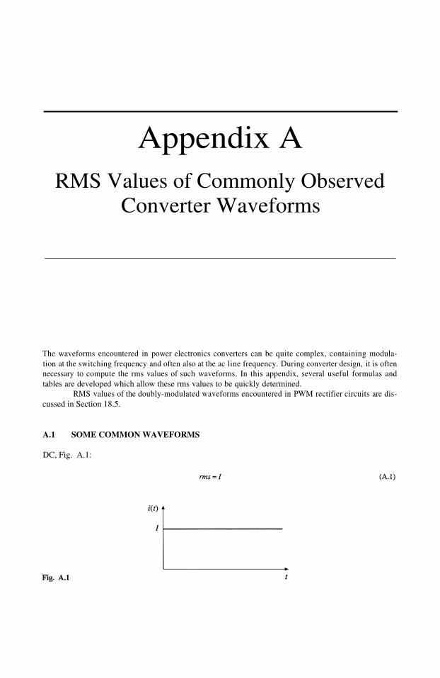
DC, Fig. A.1:

806 RMS Values of Commonly Observed Converter Waveforms
DC plus linear ripple, Fig. A.2:
Square wave, Fig. A.3:
Sine wave, Fig. A.4:
Pulsating waveform, Fig. A.5:

A.1 Some Common Waveforms 807
Pulsating waveform with linear ripple, Fig. A.6:
Triangular waveform, Fig. A.7:
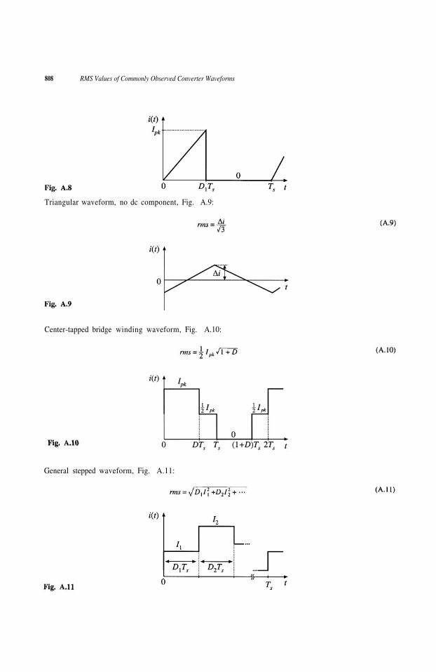
Triangular waveform, Fig. A.8:
808 RMS Values of Commonly Observed Converter Waveforms
Triangular waveform, no dc component, Fig. A.9:
Center-tapped bridge winding waveform, Fig. A.10:
General stepped waveform, Fig. A.11:

A.2 General Piecewise Waveform 809
A.2 GENERAL PIECEWISE WAVEFORM
For a periodic waveform composed of n piecewise segments as in Fig. A.12, the rms value is
where is the duty cycle of segment k, and is the contribution of segment k. The depend on theshape of the segments—several common segment shapes are listed below:
Constant segment, Fig. A.13:
Triangular segment, Fig. A.14:

810 RMS Values of Commonly Observed Converter Waveforms
Trapezoidal segment, Fig. A.15:
Sinusoidal segment, half or full period, Fig. A.16:
Sinusoidal segment, partial period: as in Fig. A.17, a sinusoidal segment of less than one half-period,which begins at angle and ends at angle The angles and are expressed in radians:

A.2 General Piecewise Waveform 811
ExampleA transistor current waveform contains a current spike due to the stored charge of a freewheel-
ing diode. The observed waveform can be approximated as shown in Fig. A1.18. Estimate the rms cur-rent.
The waveform can be divided into six approximately linear segments, as shown. The andfor each segment are
1. Triangular segment:
2. Constant segment:
3. Trapezoidal segment:
4. Constant segment:
5. Triangular segment:
6. Zero segment:

812 RMS Values of Commonly Observed Converter Waveforms
The rms value is
Even though its duration is very short, the current spike has a significant impact on the rms value of thecurrent—without the current spike, the rms current is approximately 2.0 A.

Appendix BSimulation of Converters
Computer simulation can be a powerful tool in the engineering design process. Starting from designspecifications, an initial design typically includes selection of system and circuit configurations, as wellas component types and values. In this process, component and system models are constructed based onvendor-supplied data, and by applications of analysis and modeling techniques. These models, validatedby experimental data whenever possible, are the basis upon which the designer can choose parametervalues and verify the achieved performance against the design specifications. One must take into accountthe fact that actual parameter values will not match their nominal values because of inevitable productiontolerances, changes in environmental conditions (such as temperature), and aging. In the design verifica-tion step, worst-case analysis (or other reliability and production yield analysis) is performed to judgewhether the specifications are met under all conditions, i.e., for expected ranges of component parametervalues. Computer simulation is very well suited for this task: using reliable models and appropriate sim-ulation setups, the system performance can be tested for various sets of component parameter values.One can then perform design iterations until the worst-case behavior meets specifications, or until thesystem reliability and production yield are acceptably high.
In the design verification of power electronic systems by simulation, it is often necessary to usecomponent and system models of various levels of complexity:
1. Detailed, complex models that attempt to accurately represent physical behavior of devices. Such modelsare necessary for tasks that involve finding switching times, details of switching transitions and switchingloss mechanisms, or instantaneous voltage and current stresses. Component vendors often provide librar-ies of such device models. To complete a detailed circuit model, one must also carefully examine effects ofpackaging and board interconnects. With fast-switching power semiconductors, simulation time steps of afew nanoseconds or less may be required, especially during on/off switching transitions. Because of thecomplexity of detailed device models, and the fine time resolution, the simulation tasks can be very timeconsuming. In practice, time-domain simulations using detailed device models are usually performed only

814 Simulation of Converters
on selected parts of the system, and over short time intervals involving a few switching cycles at most.Devices for power converters, and detailed physical device modeling, are areas of active research anddevelopment beyond the scope of this book.
Simplified device models. Since an on/off switching transition usually takes a small fraction of a switchingcycle, the basic operation of switching power converters can be explained using simplified, idealizeddevice models. For example, a MOSFET can be modeled as a switch with a small (ideally zero) on-resis-tance when on, and a very large off-resistance (ideally an open circuit) when off. Such simplified mod-els yield physical insight into the basic operation of switching power converters, and provide the startingpoint for developments of analytical models described throughout this book. Simplified device models arealso useful for time-domain simulations aimed at verifying converter and controller operation, switchingripples, current and voltage stresses, and responses to load or input transients. Since device models aresimple, and details of switching transitions are ignored, tasks that require simulations over many switchingcycles can be completed efficiently using general-purpose circuit simulators. In addition, specialized toolshave been developed to support fast transient simulation of switching power converters based on idealized,piecewise-linear device models [1-7], or a combination of piecewise-linear and nonlinear models [8].
Averaged converter models. Averaged models that are well suited for prediction of converter steady-stateand dynamic responses are discussed throughout this book. These models are essential design toolsbecause they provide physical insight and lead to analytical results that can be used in the design processto select component parameter values for a given set of specifications. In the design verification step, sim-ulations of averaged converter models can be performed to test for losses and efficiency, steady-state volt-ages and currents, stability, and large-signal transient responses. Since switching transitions and ripplesare removed by averaging, simulations over long time intervals and over many sets of parameter valuescan be completed efficiently. As a result, averaged models are also well suited for simulations of largeelectronic systems that include switching converters. Furthermore, since large-signal averaged models arenonlinear, but time-invariant, small-signal ac simulations can be used to generate various frequencyresponses of interest. Selected references on averaged converter modeling for simulation are listed at theend of this chapter [9-18].
2.
3.
Averaged models for computer simulation are covered in this appendix. Based on the material presentedin Section 7.4, averaged switch models for computer simulation of converters operating in continuousconduction mode are described in Section B.1. Application examples include finding SEPIC dc conver-sion ratio and efficiency, and large-signal transient responses of a buck-boost converter. Section B.2describes an averaged switch model suitable for simulation of converters that may operate either in con-tinuous conduction mode or in discontinuous conduction mode. Application examples include findingSEPIC open-loop frequency responses in CCM and DCM, loop-gain, phase margin and closed-loopresponses of a buck voltage regulator, and current harmonics in a DCM boost rectifier. Based on theresults from Chapter 12, a simulation model for converters with current programmed control is describedin Section B.3, together with a buck converter example that compares control-to-output frequencyresponses with current programmed control against duty-cycle control.
It is assumed that the reader is familiar with basics of Spice circuit simulations. All simulationmodels and examples in this appendix are prepared using the PSpice circuit simulator [19]. Netlists areincluded to help explain details of model implementation and simulation analysis options. Usually,instead of writing netlists, the user would enter circuit diagrams and analysis options from a front-endschematic capture tool. The examples and the library switch.lib of subcircuit models described in thisappendix are available on-line. Similar models and examples can be constructed for use with other simu-lation tools.
B.1 Averaged Switch Models for Continuous Conduction Mode 815
B.1 AVERAGED SWITCH MODELS FOR CONTINUOUS CONDUCTION MODE
The central idea of the averaged switch modeling described in Section 7.4 is to identify a switch networkin the converter, and then to find an averaged circuit model. The resulting averaged switch model canthen be inserted into the converter circuit to obtain a complete model of the converter. An important fea-ture of the averaged switch modeling approach is that the same model can be used in many different con-verter configurations; it is not necessary to rederive an averaged equivalent circuit for each particularconverter. This feature is also very convenient for construction of averaged circuit models for simulation.A general-purpose subcircuit represents a large-signal nonlinear averaged switch model. The converteraveraged circuit for simulation is then obtained by replacing the switch network with this subcircuit.Based on the discussion in Section 7.4, subcircuits that represent CCM averaged switch models aredescribed in this section, together with application examples.
B.1.1 Basic CCM Averaged Switch Model
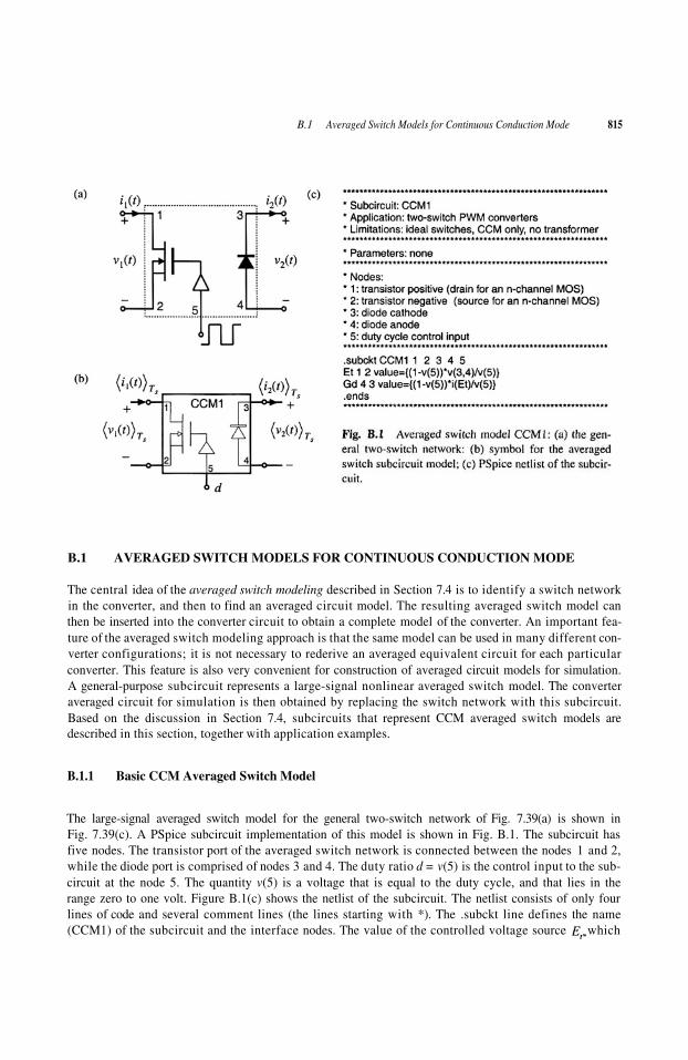
The large-signal averaged switch model for the general two-switch network of Fig. 7.39(a) is shown inFig. 7.39(c). A PSpice subcircuit implementation of this model is shown in Fig. B.1. The subcircuit hasfive nodes. The transistor port of the averaged switch network is connected between the nodes 1 and 2,while the diode port is comprised of nodes 3 and 4. The duty ratio d = v(5) is the control input to the sub-circuit at the node 5. The quantity v(5) is a voltage that is equal to the duty cycle, and that lies in therange zero to one volt. Figure B.1(c) shows the netlist of the subcircuit. The netlist consists of only fourlines of code and several comment lines (the lines starting with *). The .subckt line defines the name(CCM1) of the subcircuit and the interface nodes. The value of the controlled voltage source which
816 Simulation of Converters
models the transistor port of the averaged switch network, is written according to Eq. (7.136):
Note that v(3,4) in the subcircuit of Fig. B.1 is equal to the switch network independent inputAlso, d(t) = v(5), and The value of the controlled current source whichmodels the diode port, is computed according to Eq. (7.137):
The switch network independent input equals the current through the controlled voltagesource The ends line completes the subcircuit netlist. The subcircuit CCM1 is included in the modellibrary switch.lib.
An advantage of the subcircuit CCM1 of Fig. B.1 is that it can be used to construct an averagedcircuit model for simulation of any two-switch PWM converter operating in continuous conductionmode, subject to the assumptions that the switches can be considered ideal, and that the converter doesnot include a step-up or step-down transformer. The subcircuit can be further refined to remove theselimitations. In converters with an isolation transformer, the right-hand side of Eqs. (B.1) and (B.2)should be divided by the transformer turns ratio. Inclusion of switch conduction losses is discussed in thenext section.
A disadvantage of the model in Fig. B.1 is that Eqs. (B.1) and (B.2) have a discontinuity at dutycycle equal to zero. In applications of the subcircuit, it is necessary to restrict the duty-cycle to the range
Following the approach of this section, subcircuits can be constructed for the large-signal aver-aged models of the buck switch network (see Fig. 7.50(a), and Eqs. (7.150)), and the boost switch net-work (see Fig. 7.46(a) and Eqs. (7.146)). An advantage of these models is that their defining equations donot have the discontinuity problem at d = 0.
B.1.2 CCM Averaged Switch Model that Includes Switch Conduction Losses
Let us modify the model of Fig. B.1 to include switch conduction losses. Figure B.2 shows simple devicemodels that include transistor and diode conduction losses in the general two-switch network ofFig. B.1(a). The transistor is modeled as an ideal switch in series with an on-resistance The diode ismodeled as an ideal diode in series with a forward voltage drop and resistance
Construction of dc equivalent circuits to find dc conversion ratio and efficiency of converters isdiscussed in Chapter 3. Derivation of an averaged switch model that includes conduction losses arisingfrom and is described in Section 7.4.5. Following the same averaged switch modeling approach,we can find the following relationships that describe the averaged switch model for the switch network ofFig. B.2:
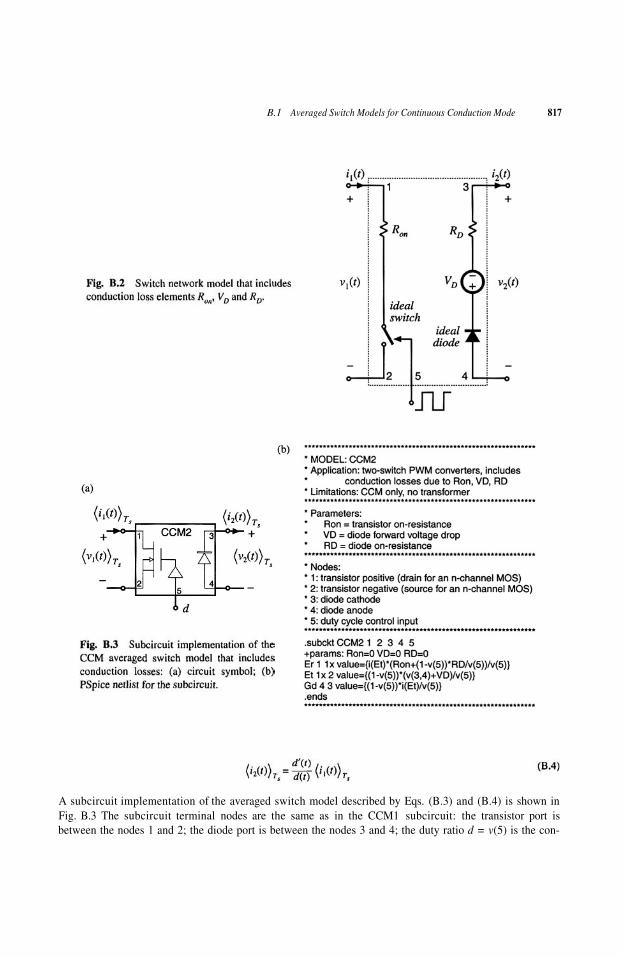
A subcircuit implementation of the averaged switch model described by Eqs. (B.3) and (B.4) is shown inFig. B.3 The subcircuit terminal nodes are the same as in the CCM1 subcircuit: the transistor port isbetween the nodes 1 and 2; the diode port is between the nodes 3 and 4; the duty ratio d = v(5) is the con-
B.1 Averaged Switch Models for Continuous Conduction Mode 817

818 Simulation of Converters
trol input to the subcircuit at the node 5. Two controlled voltage sources in series, and are used togenerate the port 1 (transistor) averaged voltage according to Eq. (B.3). The controlled voltage sourcemodels the voltage drop across the equivalent resistance in Eq. (B.3). Note thatthis equivalent resistance is a nonlinear function of the switch duty cycle The controlled voltagesource shows how the port 1 (transistor) averaged voltage depends on the port 2 (diode) averaged volt-age. The controlled current source models the averaged diode current according to Eq. (B.4). Thesubcircuit CCM2 has three parameters and that can be specified when the subcircuit is usedin a converter circuit. The default values of the subcircuit parameters, and aredefined in the .subckt line. These values correspond to the ideal case of no conduction losses. The subcir-cuit CCM2 is included in the model library switch.lib.
The model of Fig. B.3 is based on the simple device models of Fig. B.2. It is assumed thatinductor current ripples are small and that the converter operates in continuous conduction mode. Manypractical converters, however, must operate in discontinuous conduction mode at low duty cycles wherethe diode forward voltage drop is comparable to or larger than the output voltage. In such cases, themodel of Fig. B.2, which includes as a fixed voltage generator, gives incorrect, physically impossibleresults for polarities of converter voltages and currents, losses and efficiency.
B.1.3 Example: SEPIC DC Conversion Ratio and Efficiency
Let us consider an example of how the subcircuit CCM2 can be used to generate dc conversion ratio andefficiency curves for a CCM converter. As an example, Figure B.4 shows a SEPIC averaged circuitmodel. The converter circuit can be found in Fig. 6.38(a), or in Fig. 7.37. To construct the averaged cir-cuit model for simulation, the switch network is replaced by the subcircuit CCM2. In the converter netlistshown in Fig. B.4, the line shows how the subcircuit is connected to other parts of the converter.The switch duty cycle is set by the voltage source All other parts of the converter circuit are simplycopied to the averaged circuit model. Inductor w ind ing resistances and are

B.1 Averaged Switch Models for Continuous Conduction Mode 819
included to model copper losses of the inductors and respectively. The switch conduction lossparameters are defined by the .param line in the netlist: Notice howthese values are passed to the subcircuit CCM2 in the line. In this example, all other losses in theconverter are neglected. A dc sweep analysis (see the .dc line in the netlist) is set to vary the dc voltagesource from 0.1 V to 1 V, in 0.01 V increments, which corresponds to varying the switch duty cycleover the range from D = 0.1 to D = 1. The range of duty cycles from zero to 0.1 is not covered because ofthe model discontinuity problem at D = 0 (discussed in Section B.1.1), and because the model predic-tions for conduction losses at low duty cycles are not valid, as discussed in Section B.1.2. The dc sweepanalysis is repeated for values of the switch on-resistance in the range from to in
increments (see the .step line in the netlist). The .lib line refers to the switch.lib library, which con-tains definitions of the subcircuit CCM2 and all other subcircuit models described in this appendix.
Simulation results for the dc output voltage V and the converter efficiency are shown inFig. B.5. Several observations can be made based on the modeling approach and discussions presented inChapter 3. At low duty cycles, efficiency drops because the diode forward voltage drop is comparable tothe output voltage. At higher duty cycles, the converter currents increase, so that the conduction lossesincrease. Eventually, for duty cycles approaching 1, both the output voltage and the efficiency approachzero. Given a desired dc output voltage and efficiency, the plots in Fig. B.5 can be used to select the tran-sistor with an appropriate value of the on-resistance.
B.1.4 Example: Transient Response of a Buck–Boost Converter
In addition to steady-state conversion characteristics, it is often of interest to investigate converter tran-sient responses. For example, in voltage regulator designs, it is necessary to verify whether the outputvoltage remains within specified limits when the load current takes a step change. As another example,during a start-up transient when the converter is powered up, converter components can be exposed tosignificantly higher stresses than in steady state. It is of interest to verify that component stresses are

820 Simulation of Converters
within specifications or to make design modifications to reduce the stresses. In these examples, transientsimulations can be used to test for converter responses.
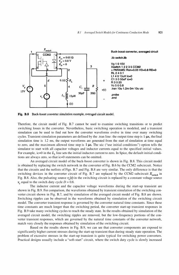
Transient simulations can be performed on the converter switching circuit model or on the con-verter averaged circuit model. As an example, let us apply these two approaches to investigate a start-uptransient response of the buck-boost converter shown in Fig. B.6.
Figure B.7 shows a switching circuit model of the buck-boost converter. The inductor windingresistance is included to model the inductor copper losses. The MOSFET is modeled as a voltage-con-trolled switch controlled by a pulsating voltage source The switch .model line specifies the switchon-resistance and the switch off-resistance The switch is on when the con-trolling voltage is greater than and off when the controlling voltage is less thanThe pulsating source has the pulse amplitude equal to 10 V. The period is the rise andfall times are ns, and the pulse width is . The switch duty cycle is
The built-in nonlinear Spice model is used for the diode. In the diode.model statement, only the parameter is specified, to set the forward voltage drop across the diode. Theswitch and the diode models used in this example are very simple. Conduction losses are modeled in asimple manner, and details of complex device behavior during switching transitions are neglected.
B.1 Averaged Switch Models for Continuous Conduction Mode 821
Therefore, the circuit model of Fig. B.7 cannot be used to examine switching transitions or to predictswitching losses in the converter. Nevertheless, basic switching operation is modeled, and a transientsimulation can be used to find out how the converter waveforms evolve in time over many switchingcycles. Transient simulation parameters are defined by the .tran line: the output time step is the finalsimulation time is 1.2 ms, the output waveforms are generated from the start of simulation at time equalto zero, and the maximum allowed time step is The uic (“use initial conditions”) option tells thesimulator to start with all capacitor voltages and inductor currents equal to the specified initial values.For example, ic=0 in the line sets the initial inductor current to zero. In Spice, the default initial condi-tions are always zero, so that ic=0 statements can be omitted.
An averaged circuit model of the buck-boost converter is shown in Fig. B.8. This circuit modelis obtained by replacing the switch network in the converter of Fig. B.6 by the CCM2 subcircuit. Noticethat the circuits and the netlists of Figs. B.7 and Fig. B.8 are very similar. The only difference is that theswitching devices in the converter circuit of Fig. B.7 are replaced by the CCM2 subcircuit inFig. B.8. Also, the pulsating source in the switching circuit is replaced by a constant voltage source
equal to the switch duty cycle D = 0.8.The inductor current and the capacitor voltage waveforms during the start-up transient are
shown in Fig. B.9. For comparison, the waveforms obtained by transient simulation of the switching con-verter circuit shown in Fig. B.7, and by simulation of the averaged circuit model of Fig. B.8 are shown.Switching ripples can be observed in the waveforms obtained by simulation of the switching circuitmodel. The converter transient response is governed by the converter natural time constants. Since thesetime constants are much longer than the switching period, the converter start-up transient responses inFig. B.9 take many switching cycles to reach the steady state. In the results obtained by simulation of theaveraged circuit model, the switching ripples are removed, but the low-frequency portions of the con-verter transient responses, which are governed by the natural time constants of the converter network,match very closely the responses obtained by simulation of the switching circuit.
Based on the results shown in Fig. B.9, we can see that converter components are exposed tosignificantly higher current stresses during the start-up transient than during steady state operation. Theproblem of excessive stresses in the start-up transient is quite typical for switching power converters.Practical designs usually include a “soft-start” circuit, where the switch duty cycle is slowly increased

822 Simulation of Converters
from zero to the steady-state value to reduce start-up transient stresses.This simulation example illustrates how an averaged circuit model can be used in place of a
switching circuit model to investigate converter large-signal transient responses. An advantage of theaveraged circuit model is that transient simulations can be completed much more quickly because theaveraged model is time invariant, and the simulator does not spend time computing the details of the fastswitching transitions. This advantage can be important in simulations of larger electronic systems thatinclude switching power converters. Another important advantage also comes from the fact that the aver-aged circuit model is nonlinear but time-invariant: ac simulations can be used to linearize the model andgenerate small-signal frequency responses of interest. This is not possible with switching circuit models.Examples of small-signal ac simulations can be found in Sections B.2 and B.3.
B.2 COMBINED CCM/DCM AVERAGED SWITCH MODEL
The models and examples of Section B.1 are all based on the assumption that the converters operate incontinuous conduction mode (CCM). As discussed in Chapters 5 and 11, all converters containing adiode rectifier operate in discontinuous conduction mode (DCM) if the load cuitent is sufficiently low. Insome cases, converters are purposely designed to operate in DCM. It is therefore of interest to develop
B.2 Combined CCM/DCM Averaged Switch Model 823
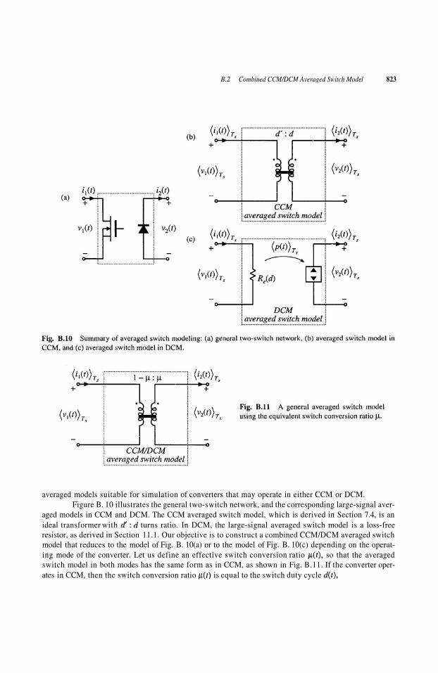
averaged models suitable for simulation of converters that may operate in either CCM or DCM.Figure B. 10 illustrates the general two-switch network, and the corresponding large-signal aver-
aged models in CCM and DCM. The CCM averaged switch model, which is derived in Section 7.4, is anideal transformer with turns ratio. In DCM, the large-signal averaged switch model is a loss-freeresistor, as derived in Section 11.1. Our objective is to construct a combined CCM/DCM averaged switchmodel that reduces to the model of Fig. B. 10(a) or to the model of Fig. B. 10(c) depending on the operat-ing mode of the converter. Let us define an effective switch conversion ratio so that the averagedswitch model in both modes has the same form as in CCM, as shown in Fig. B.11. If the converter oper-ates in CCM, then the switch conversion ratio is equal to the switch duty cycle

824 Simulation of Converters
If the converter operates in DCM, then the effective switch conversion ratio can be computed so that theterminal characteristics of the averaged-switch model of Fig. B.11 match the terminal characteristics ofthe loss-free resistor model of Fig. B.10(c). Matching the port 1 characteristics gives
which can be solved for the switch conversion ratio
It can be verified that matching the port 2 characteristics of the models in Figs. B.10(c) and B.11 givesexactly the same result for the effective switch conversion ratio in DCM.
The switch conversion ratio can be considered a generalization of the duty cycle d(t) ofCCM switch networks. Based on this approach, models and results developed for converters in CCM canbe used not only for DCM but also for other operating modes or even for other converter configurationsby simply replacing the switch duty cycle d(t) with the appropriate switch conversion ratio [21-24].For example, if M(d) is the conversion ratio in CCM, then with given by Eq. (B .7), is the conver-sion ratio in DCM. The switch conversion ratio in DCM depends on the averaged terminal voltage andcurrent, as well as the switch duty cycle d through the effective resistance If the converteris completely unloaded, then the average transistor current is zero, and the DCM switch conver-sion ratio becomes As a result, the dc output voltage attains the maximum possible value
This is consistent with the results of the steady-state DCM analyses in Chapter 5 and Sec-tion 11.1.
To construct a combined CCM/DCM averaged switch model based on the general averagedswitch model of Fig. B.11, it is necessary to specify which of the two expressions for the switch conver-sion ratio to use: Eq. (B.5), which is valid in CCM, or Eq. (B.7), which is valid in DCM. At the CCM/DCM boundary, these two expressions must give the same result, If the load current decreases fur-ther, the converter operates in DCM, the average switch current decreases, and the DCM switchconversion ratio in Eq. (B.7) becomes greater than the switch duty cycle d. We conclude that the correctvalue of the switch conversion ratio, which takes into account operation in CCM or DCM, is the larger ofthe two values computed using Eq. (B.5) and Eq. (B.7).
Figure B.12 shows an implementation of the combined CCM/DCM model as a PSpice subcir-cuit CCM-DCM1. This subcircuit has the same five interface nodes as the subcircuits CCM1 and CCM2of Section B.1. The controlled sources and model the port 1 (transistor) and port 2 (diode) averagedcharacteristics, as shown in Fig. B.11. The switch conversion ratio is equal to the voltage at thesubcircuit node u. The controlled voltage source computes the switch conversion ratio as the greaterof the two values obtained from Eqs. (B.5) and (B.7). The controlled current source the zero-valuevoltage source and the resistor form an auxiliary circuit to ensure that the solution found by thesimulator has the transistor and the diode currents with correct polarities, Thesubcircuit parameters are the inductance L relevant for CCM/DCM operation, and the switching fre-quency The default values in the subcircuit are arbitrarily set to
The PSpice subcircuit CCM-DCM1 of Fig. B.12 can be used for dc, ac, and transient simula-

B.2 Combined CCM/DCM Averaged Switch Model 825
tions of PWM converters containing a transistor switch and a diode switch. This subcircuit is included inthe model library switch.lib. It can be modified further for use in converters with isolation transformer.
B.2.1 Example: SEPIC Frequency Responses
As an example, Fig. B.13 shows a SEPIC circuit and the averaged circuit model obtained by replacingthe switch network with the CCM-DCM1 subcircuit of Fig. B.12. A part of the circuit netlist is includedin Fig. B.13. The connections and the parameters of the CCM-DCM1 subcircuit are defined by theline. In the SEPIC, the inductance parameter is equal to the parallel combination of and
The voltage source sets the quiescent value of the duty cycle to D = 0.4, and the small-signal acvalue to simulation is performed on a linearized circuit model, so that amplitudes of all small-signal ac waveforms are directly proportional to the amplitude of the ac input, regardless of the input acamplitude value. For example, the control-to-output transfer function is in thecircuit of Fig. B.13(b). We can set the input ac amplitude to 1, so that the control-to-output transfer func-tion can be measured directly as v(5). This setup is just for convenience in finding small-signal fre-quency responses by simulation. For measurements of converter transfer functions in an experimentalcircuit (see Section 8.5), the actual amplitude of the small-signal ac variation would be set to a fractionof the quiescent duty cycle D. Parameters of the ac simulation are set by the .ac line in the netlist: the sig-nal frequency is swept from the minimum frequency of 5 Hz to the maximum frequency of 50 kHz in201 points per decade.
Figure B.14 shows magnitude and phase responses of the control-to-output transfer functionobtained by ac simulations for two different values of the load resistance: for which the con-verter operates in CCM, and for which the converter operates in DCM. For these two operating

826 Simulation of Converters
points, the quiescent (dc) voltages and currents in the circuit are nearly the same. Nevertheless, the fre-quency responses are qualitatively very different in the two operating modes. In CCM, the converterexhibits a fourth-order response with two pairs of high-Q complex-conjugate poles and a pair of com-plex-conjugate zeros. Another RHP (right-half plane) zero can be observed at frequencies approaching50 kHz. In DCM, there is a dominant low-frequency pole followed by a pair of complex-conjugate polesand a pair of complex-conjugate zeros. The frequencies of the complex poles and zeros are very close invalue. A high-frequency pole and a RHP zero contribute additional phase lag at higher frequencies.
In the design of a feedback controller around a converter that may operate in CCM or in DCM,one should take into account that the crossover frequency, the phase margin, and the closed-loopresponses can be substantially different depending on the operating mode. This point is illustrated by theexample of the next section.

B.2 Combined CCM/DCM Averaged Switch Model 827
B.2.2 Example: Loop Gain and Closed-Loop Responses of a Buck Voltage Regulator
A controller design for a buck converter example is discussed in Section 9.5.4. The converter and theblock diagram of the controller are shown in Fig. 9.22. This converter system is designed to regulate thedc output voltage at V = 15 V for the load current up to 5 A. Let us test this design by simulation. Anaveraged circuit model of a practical realization of the buck voltage regulator described in Section 9.5.4is shown in Fig. B.15. The MOSFET and the diode switch are replaced by the averaged switch modelimplemented as the CCM-DCM1 subcircuit. The pulse-width modulator with is modeledaccording to the discussion in Section 7.6 as a dependent voltage source controlled by the PWMinput voltage The value of is equal to times the PWM input voltage with a limitfor the minimum value set to 0.1 V, and a limit for the maximum value set to 0.9 V. The output of thepulse-width modulator is the control duty-cycle input to the CCM-DCM1 averaged switch subcircuit.Given the specified limits for the switch duty cycle d(t) can take values in the range:
where Practical PWM integrated circuits often have a limit for themaximum possible duty cycle. The voltage sensor and the compensator are implemented around an op-amp LM324. With very large loop gain in the system, the steady-state error voltage is approximatelyzero, i.e., the dc voltages at the plus and the minus inputs of the op-amp are almost the same,

828 Simulation of Converters
As a result, the quiescent (dc) output voltage V is set by the reference voltage and the voltage dividercomprised of
By setting the ac reference voltage to zero, the combined transfer function of the voltage sensor andthe compensator can be found as:
This transfer function can be written in factored pole-zero form as
where

B.2 Combined CCM/DCM Averaged Switch Model 829
and
The design described in Section 9.5.4 resulted in the following values for the gain and the corner fre-quencies:
Eqs. (B.10) and (B.13) to (B.17) can be used to select the circuit parameter values. Let us (somewhatarbitrarily) choose Then, from Eq. (B.14), we have and Eq. (B.16) yields
From Eq. (B.13) we obtain and Eq. (B. 15) gives Finally,is found from Eq. (B.10). The voltage regulator design can now be tested by simulations of
the circuit in Fig. B.15.Loop gains can be obtained by simulation using exactly the same techniques described in Sec-
tion 9.6 for experimental measurement of loop gains [20]. Let us apply the voltage injection technique ofSection 9.6.1. An ac voltage source is injected between the compensator output and the PWM input.This is a good injection point since the output impedance of the compensator built around the op-amp issmall, and the PWM input impedance is very large (infinity in the circuit model of Fig. B.15). With theac source amplitude set (arbitrarily) to 1, and no other ac sources in the circuit, ac simulations are per-formed to find the loop gain as
To perform ac analysis, the simulator first solves for the quiescent (dc) operating point. The circuit isthen linearized at this operating point, and small-signal frequency responses are computed for the speci-fied range of signal frequencies. Solving for the quiescent operating point involves numerical solution ofa system of nonlinear equations. In some cases, the numerical solution does not converge and the simula-tion is aborted with an error message. In particular, convergence problems often occur in circuits withfeedback, especially when the loop gain at dc is very large. This is the case in the circuit of Fig. B.15. Tohelp convergence when the simulator is solving for the quiescent operating point, one can specifyapproximate or expected values of node voltages using the .nodeset line as shown in Fig. B.15. In thiscase, we know by design that the quiescent output voltage is close to 15 V (v(3) = 15), that the negativeinput of the op-amp is very close to the reference (v(5) = 5), and that the quiescent duty cycle is approxi-mately so that v(8) = 0.536 V. Given these approximate node voltages, the numericalsolution converges, and the following quiescent operating points are found by the simulator for two val-ues of the load resistance R:

830 Simulation of Converters
For the nominal load resistance the converter operates in CCM, so thatthe same dc output voltage is obtained for a lower value of the quiescent duty cycle, which means that theconverter operates in DCM.
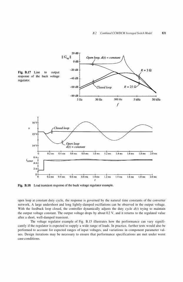
The magnitude and phase responses of the loop gain found for the operating points given byEqs. (B.19) and (B.20) are shown in Fig. B.16. For the crossover frequency is andthe phase margin is very close to the values that we designed for inSection 9.5.4. At light load, for the loop gain responses are considerably different because theconverter operates in DCM. The crossover frequency drops to while the phase margin is
The magnitude responses of the line-to-output transfer function are shown in Fig. B.17, againfor two values of the load resistance, The open-loop responses are obtained bybraking the feedback loop at node 8, and setting the dc voltage at this node to the quiescent value D ofthe duty cycle. For the open-loop and closed-loop responses can be compared to the theoreticalplots shown in Fig. 9.32. At 100 Hz, the closed-loop magnitude response is A 1 V,100 Hz variation in would induce a 12 mV variation in the output voltage v(t). For theclosed loop magnitude response is which means that the 1 V, 100 Hz variation inwould induce a 20 mV variation in the output voltage. Notice how the regulator performance in terms ofrejecting the input voltage disturbance is significantly worse at light load than at the nominal load.
A test of the transient response to a step change in load is shown in Fig. B.18. The load currentis in i t ially equal to 1.5 A, and increases to at t = 0.1 tns. When the converter is operated in
For
B.2 Combined CCM/DCM Averaged Switch Model 831
open loop at constant duty cycle, the response is governed by the natural time constants of the converternetwork, A large undershoot and long lightly-damped oscillations can be observed in the output voltage.With the feedback loop closed, the controller dynamically adjusts the duty cycle d(t) trying to maintainthe output voltage constant. The output voltage drops by about 0.2 V, and it returns to the regulated valueafter a short, well-damped transient.
The voltage regulator example of Fig. B.15 illustrates how the performance can vary signifi-cantly if the regulator is expected to supply a wide range of loads. In practice, further tests would also beperformed to account for expected ranges of input voltages, and variations in component parameter val-ues. Design iterations may be necessary to ensure that performance specifications are met under worstcase conditions.

832 Simulation of Converters
B.2.3 Example: DCM Boost Rectifier
Converters switching at frequencies much above the ac line frequency can be used to construct near-idealrectifiers where power is taken from the ac line without generation of line current harmonics. Approachesto construction of low-harmonic rectifiers are discussed in Chapter 18. One simple solution is based onthe boost converter operating in discontinuous conduction mode, as described in Section 18.2.1. When aboost DCM converter operates at a constant switch duty cycle, the input current approximately followsthe input voltage. The DCM effective resistance is an approximation of the emulated resis-tance of the DCM boost rectifier. Ac line current harmonics are not zero, but the rectifier can still bedesigned to meet harmonic limits. In this section we consider a DCM boost rectifier example and test itsperformance by simulation.
An averaged circuit model of the boost DCM rectifier is shown in Fig. B.19. Full-wave rectified120 Vrms, 50 Hz ac line voltage is applied to the input of the boost converter. The converter switches arereplaced by the CCM-DCM1 averaged switch subcircuit. It is desired to regulate the dc output voltage atV = 300 V at output power up to across the load R. The switching frequency is
Let us select the inductance L so that the converter always operates in DCM. FromEq. (18.24), the condition for DCM is:
where is the emulated resistance of the rectifier and is the peak of the ac line voltage. When line

B.2 Combined CCM/DCM Averaged Switch Model 833
current harmonics and losses are neglected, the rectifier emulated resistance at the specified loadpower P is
Given and found from Eq. (B.22), Eq. (B.21) gives The selected inductanceis A low-bandwidth voltage feedback loop is closed around the converter to regulate the dcoutput voltage. The output voltage is sensed and compared to the reference A PI compensator is con-structed around the LM324 op-amp. The output of the compensator is the input to the pulse-widthmodulator. By adjusting the switch duty ratio d, adjusts the emulated resistance ofthe rectifier, and thereby controls the power taken from the ac line. In steady state, the input powermatches the output power. The dc output voltage V is regulated at the value set by the reference voltage
and the voltage divider composed of and as follows:
Modeling of the low-bandwidth voltage regulation loop is discussed in Section 18.4.2.It is of interest to find ac line current harmonics. First, a long transient simulation is performed
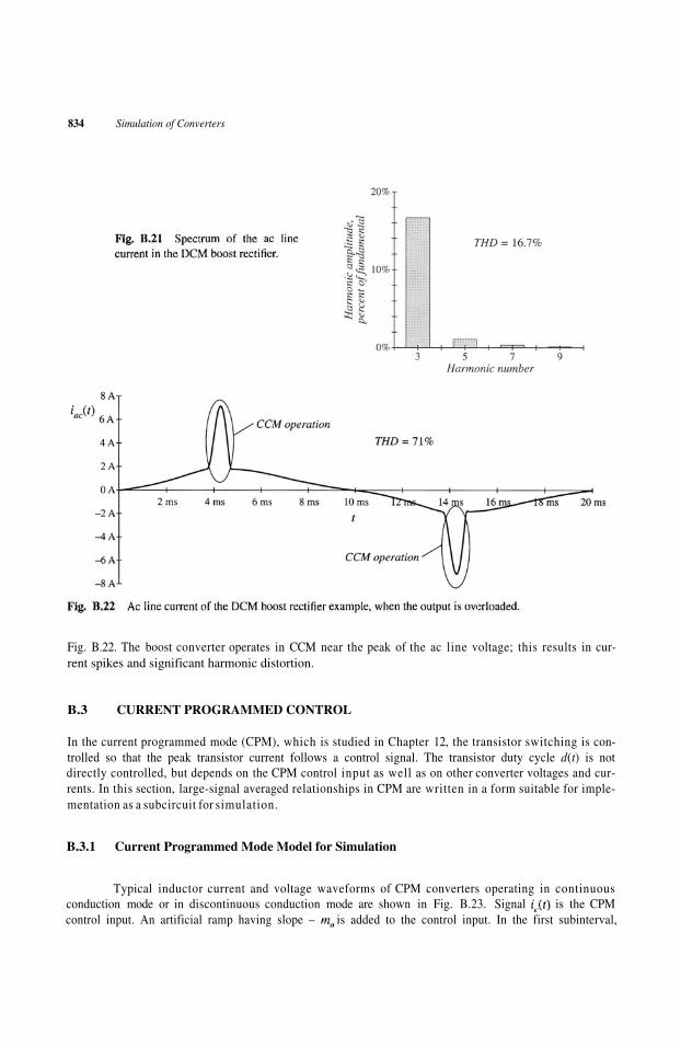
to reach steady-state operation. Then, current harmonics are computed using Fourier analysis applied tothe ac line current waveform during one line cycle in steady state. Figure B.20 shows the steady-state ac line current and output voltage obtained for i.e., for 100 Wof output power. The out-put voltage has a dc component equal to 300 V, and an ac ripple component at twice the line frequency.The peak-to-peak voltage ripple at twice the line frequency is approximately 8 V, which compares wellwith the value (7 V) found from Eq. (18.91). The ac line current has noticeable distortion. The spectrumof the ac line current is shown in Fig. B.21. The largest harmonic, the third, has an amplitude of 16.6% ofthe fundamental, and the total harmonic distortion is 16.7%.
We can also examine what happens if the rectifier is overloaded. The steady-state ac line currentwaveform for the case when the load resistance is and the output power is 180 W, is shown in
834 Simulation of Converters
B.3 CURRENT PROGRAMMED CONTROL
In the current programmed mode (CPM), which is studied in Chapter 12, the transistor switching is con-trolled so that the peak transistor current follows a control signal. The transistor duty cycle d(t) is notdirectly controlled, but depends on the CPM control input as well as on other converter voltages and cur-rents. In this section, large-signal averaged relationships in CPM are written in a form suitable for imple-mentation as a subcircuit for simulation.
B.3.1 Current Programmed Mode Model for Simulation
Typical inductor current and voltage waveforms of CPM converters operating in continuousconduction mode or in discontinuous conduction mode are shown in Fig. B.23. Signal is the CPMcontrol input. An artificial ramp having slope – is added to the control input. In the first subinterval,
Fig. B.22. The boost converter operates in CCM near the peak of the ac line voltage; this results in cur-rent spikes and significant harmonic distortion.

B.3 Current Programmed Control 835
when the transistor is on, the inductor current increases with slope given by:
It is assumed that voltage ripples are small so that the voltage across the inductor is approximatelyequal to the averaged value The length of the first subinterval is The transistor is turnedoff when the inductor current reaches the peak value equal to:
In the second subinterval, when the transistor is off and the diode is on, the inductor current decreaseswith a negative slope – With the assumption the voltage ripples are small, the slope is given by:
The length of the second subinterval is In CCM, the second subinterval lasts until the end of theswitching cycle. Therefore:
In DCM, the current drops to zero before the end of the switching period. The length of the second sub-interval can be computed from:

836 Simulation of Converters
If the converter operates in DCM, computed from Eq. (B.28) is smaller that 1 – d. If the converteroperates in CCM, 1 – d is smaller than computed from Eq. (B.28). In general, the length of the secondsubinterval can be found as the smaller of the two values computed using Eqs. (B.27) and (B.28).
The average inductor current can be found by computing the area under the inductor currentwaveform in Fig. B.23:
The relationship given by Eq. (B.29) is valid for both CCM and DCM provided that the second subinter-val length is computed as the smaller of the values obtained from Eqs. (B.27) and (B.28).
Based on Eqs. (B.24) to (B.29), an averaged CPM subcircuit model is constructed in the formshown in Fig. B.24. The inputs to the CPM subcircuit are the control input the mea-sured inductor current and the inductor voltages and of the two subintervals.The output of the subcircuit is the switch duty cycle d. The parameters of the CPM subcircuit are theequivalent current-sense resistance the inductance L, the switching frequency and the ampli-tude of the artificial ramp:
In the subcircuit implementation, the length of the second subinterval is computed as the smaller of thevalues given by Eqs. (B.27) and (B.28):
Next, the switch duty cycle is found by solving Eq. (B.29). There are many different ways the switchduty cycle can be expressed in terms of other quantities. Although mathematically equivalent toEq. (B.29), these different forms of solving for d result in different convergence performance of thenumerical solver in the simulator. In the CPM subcircuit available in the switch.lib library, the duty cycleis found from:

B.3 Current Programmed Control 837
which is obtained by inserting Eq. (B.25) into Eq. (B.29). This implicit expression (notice that d is onboth sides of the equation) is used by the numerical solver in the simulator to compute the switch dutycycle d.
B.3.2 Example: Frequency Responses of a Buck Converter with Current Programmed Control
To illustrate an application of the CPM subcircuit, let us consider the example buck converter circuitmodel of Fig. B.25. To construct this averaged circuit model, the switches are replaced by the CCM-DCM1 averaged switch subcircuit. The control input to the CPM subcircuit is the independent voltagesource Three dependent voltage sources are used to generate other inputs to the CPM subcircuit. Thecontrolled voltage source is proportional to the inductor current The controlled voltage source isequal to v(1) – v(3), which is equal to the voltage applied across the inductor during the first sub-interval when the transistor is on and the diode is off. The controlled voltage source is equal to v(3),which is equal to the voltage applied across the inductor during the second subinterval when thetransistor is off and the diode is on.
Ac simulations are performed at the quiescent operating point obtained for the dc value of the

838 Simulation of Converters
control input equal to At the quiescent operating point, the switch duty cycle is D = 0.676, thedc output voltage is V = 8.1 V, and the dc component of the inductor current is The converteroperates in CCM.
Magnitude and phase responses of the control-to-output transfer functions andare shown in Fig. B.26. The duty-cycle to output voltage transfer function exhibits the
familiar second-order high-Q response. Peaking in the magnitude response and a steep change in phasefrom 0° to – 180° occur around the center frequency of the pair of complex-conjugate poles. In contrast,the CPM control-to-output response has a dominant low-frequency pole. The phase lag is around – 90° ina wide range of frequencies. A high frequency pole contributes to additional phase lag at higher frequen-cies. The frequency responses of Fig. B.26 illustrate an advantage of CPM control over duty-cycle con-trol. Because of the control-to-output frequency response dominated by the single low-frequency pole, itcan be much easier to close a wide-bandwidth outer voltage feedback loop around the CPM controlledpower converter than around a converter where the duty cycle is the control input.
Another advantage of CPM control is in rejection of input voltage disturbances. Line-to-outputfrequency responses for duty-cycle control and CPM control in the buck example are compared inFig. B.27. At practically all frequencies of interest, CPM control offers more than 30 dB better attenua-tion of input voltage disturbances.
It is also interesting to compare the output impedance of the converter with duty-cycle controlversus CPM control. The results are shown in Fig. B.28. At low frequencies, duty-cycle controlled con-verter has very low output impedance determined by switch and inductor resistances. As the frequencygoes up, the output impedance increases as the impedance of the inductor increases. At the resonant fre-quency of the output LC filter, significant peaking in the output impedance of the duty-cycle controlledconverter can be observed. At higher frequencies, the output impedance is dominated by the impedanceof the filter capacitor, which decreases with frequency. In the CPM controlled converter, the low-fre-quency impedance is high. It is equal to the parallel combination of the load resistance and the CPM out-

B.3 Current Programmed Control 839
put resistance. Because of the lossless damping introduced by CPM control, the series inductor does notaffect the output impedance. As the frequency goes up, the output impedance becomes dominated by theoutput filter capacitor and it decreases with frequency. At high frequencies the output impedances of theduty-cycle and CPM controlled converters have the same asymptotes.

840 Simulation of Converters
REFERENCES
R. J. DIRKMAN, “The Simulation of General Circuits Containing Ideal Switches,” IEEE Power ElectronicsSpecialists Conference, 1987 Record, pp. 185-194.
C. J. HSIAO, R. B. RIDLEY, H. NAITOH and F. C. LEE, “Circuit-Oriented Discrete-Time Modeling and Sim-ulation of Switching Converters, IEEE Power Electronics Specialists Conference, 1987 record, pp. 167-176.
R. C. WONG, H. A. OWEN, T. G. WILSON, “An Efficient Algorithm for the Time-Domain Simulation ofRegulated Energy-Storage DC-to-DC Converters,” IEEE Transactions on Power Electronics, Vol. 2, No. 2,April 1987, pp. 154-168.
A. M. LUCIANO and A. G. M. STROLLO, “A Fast Time-Domain Algorithm for Simulation of SwitchingPower Converters,” IEEE Transactions on Power Electronics, Vol. 2, No. 3, July 1990, pp. 363-370.
D. BEDROSIAN and J. VLACH, “Time-Domain Analysis of Networks with Internally Controlled Switches,”IEEE Transactions on Circuits and Systems–I: Fundamental Theory and Applications, Vol. 39, No.3,March 1992, pp. 199-212.
and “A New Algorithm for Simulation of Power Electronic Systems UsingPiecewise-Linear Device Models,” IEEE Transactions on Power Electronics, Vol. 10, No. 3, May 1995,pp. 340-348.
“A Method for Simulation of Power Electronic Systems Using Piecewise-LinearDevice Models,” Ph.D. thesis, University of Colorado, Boulder, April 1995.
D. LI, R. TYMERSKI, T. NINOMIYA, “PECS—An Efficacious Solution for Simulating Switched Networkswith Nonlinear Elements,” IEEE Power Electronics Specialists Conference, 2000 Record, pp. 274-279,June 2000.
V. BELLO, “Computer Aided Analysis of Switching Regulators Using SPICE2,” IEEE Power ElectronicsSpecialists Conference, 1980 Record, pp. 3-11.
V. BELLO, “Using the SPICE2 CAD Package for Easy Simulation of Switching Regulators in Both Con-tinuous and Discontinuous Conduction Modes,” Proceedings of the Eighth National Solid-State PowerConversion Conference (Powercon 8), April 1981.
V. BELLO, “Using the SPICE2 CAD Package to Simulate and Design the Current Mode Converter,” Pro-ceedings of the Eleventh National Solid-State Power Conversion Conference (Powercon 11), April 1984.
D. KIMHI, S. BEN-YAAKOV, “A SPICE Model for Current Mode PWM Converters Operating Under Con-tinuous Inductor Current Conditions,” IEEE Transactions on Power Electronics, Vol. 6, No. 2, April 1991,pp. 281-286.
Y. AMRAN, F. HULIEHEL, S. BEN-YAAKOV, “A Unified SPICE Compatible Average Model of PWM Con-verters,” IEEE Transactions on Power Electronics, Vol. 6, No. 4, October 1991, pp. 585-594.
S. BEN-YAAKOV, Z. GAATON, “Generic SPICE Compatible Model of Current Feedback in Switch ModeConverters, Electronics Letters, Vol. 28, No. 14, 2nd July 1992.
S. BEN-YAAKOV, “Average Simulation of PWM Converters by Direct Implementation of Behavioral Rela-
[1]
[2]
[3]
[4]
[5]
[6]
[7]
[8]
[9]
[10]
[11]
[12]
[13]
[14]
[15]

References 841
tionships,” IEEE Applied Power Electronics Conference, 1993 Record, pp. 510-516, February 1993.
S. BEN-YAAKOV, D. ADAR, “Average Models as Tools for Studying Dynamics of Switch Mode DC-DCconverters,” IEEE Power Electronics Specialists Conference, 1994 Record, pp. 1369-1376.
V. M. CANALLI, J. A. COBOS, J. A. OLIVER, J. UCEDA, “Behavioral Large Signal Averaged Model for DC/DC Switching Power Converters,” IEEE Power Electronics Specialists Conference, 1996 Record,pp. 1675-1681.
N. JA Y A R A M, “Power Factor Correctors Based on Coupled-Inductor SEPIC andConverters with Nonlinear- Carrier Control,” IEEE Applied Power Electronics Conference, 1998 Record,pp. 468-474, February 1998.
J. KEOWN, OrCAD PSpice and Circuit Analysis, Fourth Edition, Englewood Cliffs: Prentice Hall, 2000.
P. W. TUINENGA, SPICE: A Guide to Circuit Simulation and Analysis Using PSpice, Third Edition, Engle-wood Cliffs: Prentice Hall, 1995.
V. VORPERIAN, “Simplified Analysis of PWM Converters Using the Model of the PWM Switch: Parts Iand II,” IEEE Transactions on Aerospace and Electronic Systems, Vol. AES-26, pp. 490-505, May 1990.
S. FREELAND and R. D. MIDDLEBROOK, “A Unified Analysis of Converters with Resonant Switches,”IEEE Power Electronics Specialists Conference, 1987 Record, pp. 20-30.
ARTHUR WITULSKI and ROBERT ERICKSON, “Extension of State-Space Averaging to Resonant Switches—and Beyond,” IEEE Transactions on Power Electronics, Vol. 5, No. 1, pp. 98-109, January 1990.
and “A Unified Analysis of PWM Converters in Discontinuous Modes,” IEEETransactions on Power Electronics, Vol. 6, No. 3, pp. 476-490, July 1991.
[16]
[17]
[18]
[19]
[20]
[21]
[22]
[23]
[24]

Appendix CMiddlebrook's
Extra Element Theorem
The Extra Element Theorem of R. D. Middlebrook [1–3] shows how a transfer function is changed by theaddition of an impedance to the network. The theorem allows one to determine the effects of this extraelement on any transfer function of interest, without solving the system all over again. The Extra Ele-ment Theorem is a powerful technique of design-oriented analysis. It leads to impedance inequalitieswhich guarantee that an element does not substantially alter a transfer function. The Extra Element The-orem is employed in Chapter 10, where it leads to a relatively simple methodology for designing inputfilters that do not degrade the loop gains of switching regulators. It is also employed in Section 19.4, todetermine how the load resistance affects the properties of a resonant inverter. In this appendix, Middle-brook’s Extra Element Theorem is derived, based on the principle of superposition. Its application isillustrated via examples.
C.1 BASIC RESULT
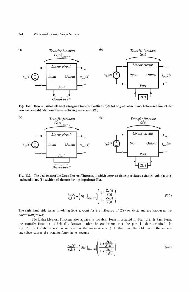
Consider the linear circuit of Fig. C.1(a). This network contains an input and an output Inaddition, it contains a port whose terminals are open-circuited. It is assumed that the transfer functionfrom to is known, and is given by
The Extra Element Theorem tells us how the transfer function G(s) is modified when an impedance Z(s)is connected between the terminals at the port, as in Fig. C.1(b). The result is
844 Middlebrook’s Extra Element Theorem
The right-hand side terms involving Z(s) account for the influence of Z(s) on G(s), and are known as thecorrection factor.
The Extra Element Theorem also applies to the dual form illustrated in Fig. C.2. In this form,the transfer function is initially known under the conditions that the port is short-circuited. InFig. C.2(b), the short-circuit is replaced by the impedance Z(s). In this case, the addition of the imped-ance Z(s) causes the transfer function to become

C.1 Basic Result 845
The and terms in Eqs. (C.2) and (C.3) are identical. By equating the G(s) expressions ofEqs. (C.2) and (C.3), one can show that
This is known as the reciprocity relationship.The quantities and can be found by measuring impedances at the port. The term
is the Thevenin equivalent impedance seen looking into the port, also known as the driving-pointimpedance. As illustrated in Fig. C.3(a), this impedance is found by setting the independent sourceto zero, and then measuring the impedance between the terminals of the port:
Thus, is the impedance between the port terminals when the input is set to zero.Determination of the impedance is illustrated in Fig. C.3(b). The term is found
under the conditions that the output is nulled to zero. A current source i(s) is connected to the ter-minals of the port. In the presence of the input signal the current i(s) is adjusted so that the output
is nulled to zero. Under these conditions, the quantity is given by

846 Middlebrook’s Extra Element Theorem
Note that nulling the output is not the same as shorting the output. If one simply shorted the output, thena current would flow through the short, which would induce voltage drops and currents in other elementsof the network. These voltage drops and currents are not present when the output is nulled. The null con-dition of Fig. C.3(b) does not employ any connections to the output of the circuit. Rather, the null condi-tion employs the adjustment of the independent sources and i(s) in a special way that causes theoutput to be zero. By superposition, can be expressed as a linear combination of andi(s); therefore, for a given it is always possible to choose an i(s) that w i l l cause to be zero.Under these nul l conditions, is measured as the ratio of v(s) to i(s). In practice, the circuit analysisto find is simpler than analysis of because the null condition causes many of the signalswithin the circuit to be zero. Several examples are given in Section C.4.
The input and output quantities need not be voltages, but could also be currents or other signalsthat can be set or nulled to zero. The next section contains a derivation of the Extra Element Theoremwith a general input u(s) and output y(s).
C.2 DERIVATION
Figure C.4(a) illustrates a general linear system having an input u(s) and an output y(s). In addition, thesystem contains an electrical port having voltage v(s) and current i(s), with the polarities illustrated. Ini-tially, the port is open-circuited: i(s) = 0. The transfer function of this system, with the port open-cir-cuited, is
The objective of the extra element theorem is to determine the new transfer function G(s) that is obtainedwhen an impedance Z(s) is connected to the port:
The situation is illustrated in Fig. C.4(b). It can be seen that the conditions at the port are now given by
C.2 Derivation 847
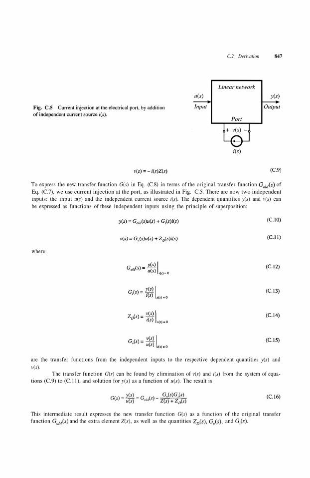
To express the new transfer function G(s) in Eq. (C.8) in terms of the original transfer function ofEq. (C.7), we use current injection at the port, as illustrated in Fig. C.5. There are now two independentinputs: the input u(s) and the independent current source i(s). The dependent quantities y(s) and v(s) canbe expressed as functions of these independent inputs using the principle of superposition:
where
are the transfer functions from the independent inputs to the respective dependent quantities y(s) andv(s).
The transfer function G(s) can be found by elimination of v(s) and i(s) from the system of equa-tions (C.9) to (C.11), and solution for y(s) as a function of u(s). The result is
This intermediate result expresses the new transfer function G(s) as a function of the original transferfunction and the extra element Z(s), as well as the quantities and

848 Middlebrook’s Extra Element Theorem
Equation (C.14) gives a direct way to find the quantity is the driving-point imped-ance at the port, when the input u(s) is set to zero. This quantity can be found either by conventional cir-cuit analysis or simulation, or by laboratory measurement.
Although and could also be determined from the definitions (C.13) and (C.15), it ispreferable to eliminate these quantities, and instead express G(s) as a function of the impedances at thegiven port. This can be accomplished via the following thought experiment. In the presence of the inputu(s), we adjust the independent current source i(s) in the special way that causes the output y(s) to benulled to zero. The impedance is defined as the ratio of v(s) to i(s) under these null conditions:
The value of i(s) that achieves the null condition can be found by setting y(s) = 0 in Eq. (C.10),as follows:
Hence, the output y(s) is nulled when the inputs u(s) and i(s) are related as follows:
Under this null condition, the voltage v(s) is given by
which follows from Eqs. (C.11) and (C.19). Substitution of Eq. (C.17) into Eq. (C.20) yields
Hence,
Solution for the quantity yields
Thus, the unknown quantities and can be related to and which are properties ofthe port at which the new impedance Z(s) will be connected, and to the original transfer function
The final step is to substitute Eq. (C.23) into Eq. (C.16), leading to

C.3 Discussion 849
This expression can be simplified as follows:
or,
This is the desired result. It states how the transfer function G(s) is modified by addition of the extra ele-ment Z(s). The right-most term in Eq. (C.26) is called the correction factor; this term gives a quantitativemeasure of the change in G(s) arising from the introduction of Z(s).
Derivation of the dual result, Eq. (C.3), follows similar steps.
C.3 DISCUSSION
The general form of the extra element theorem makes it useful for designing a system such thatunwanted circuit elements do not degrade the desirable system performance already obtained. For exam-ple, suppose that we already know some transfer function or similar quantity G(s), under simplified orideal conditions, and have designed the system such that this quantity meets specifications. We can thenuse the extra element theorem to answer the following questions:
What is the effect of a parasitic element Z(s) that was not included in the original analysis?
What happens if we later decide to add some additional components having impedance Z(s) to thesystem?
Can we establish some conditions on Z(s) that ensure that G(s) is not substantially changed?
A common application of the extra element theorem is the determination of conditions on the extra ele-ment that guarantee that the transfer function G(s) is not significantly altered. According to Eqs. (C.2)and (C.26), this will occur when the correction factor is approximately equal to unity. The conditions are:
This gives a formal way to show when an impedance can be ignored: one can plot the impedancesand and compare the results with a plot of The impedance Z(s) can be
ignored over the range of frequencies where the inequalities (C.27) are satisfied.For the dual case in which the new impedance is inserted where there was previously a short cir-
cuit, Eq. (C.3), the inequalities are reversed:

850 Middlebrook’s Extra Element Theorem
This equation shows how to limit the magnitude to avoid significantly changing the transferfunction G(s).
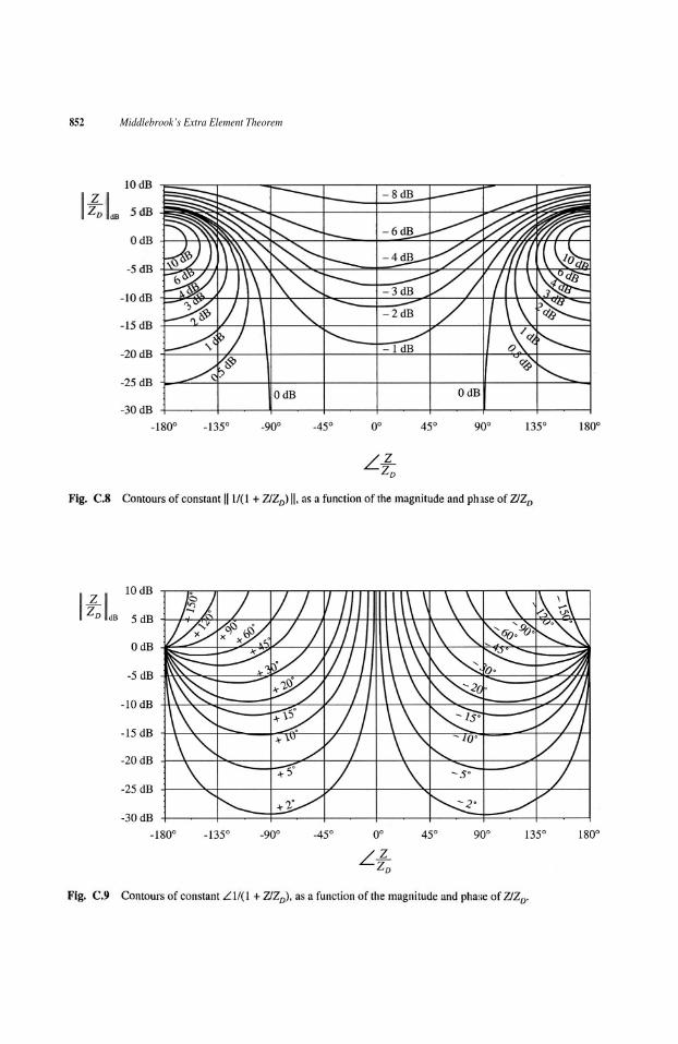
For quantitative design, Eqs. (C.27) and (C.28) raise an additional question: By what factorshould exceed (or be less than) and in order for the inequalities of Eq.(C.27) or (C.28) to be well satisfied? This question can be answered by plotting the magnitudes andphases of the correction factor terms, as a function of the magnitudes and phases of
Figure C.6 shows contours of constant as a function of the magnitude and phase ofFigure C.7 shows similar contours of constant It can be seen that, when is
less than – 20 dB, then the maximum deviation caused by the numerator term is less than±1 dB in magnitude, and less than in phase. For less than – 10 dB, the maximum deviationcaused by the numerator term is less than ± 3.5 dB in magnitude, and less than in phase.
Figures C.8 and C.9 contain contours of constant and respec-tively, as a function of the magnitude and phase of These plots contain minus signs because theterms appear in the denominator of the correction factor; otherwise, they are identical to Figs. C.6 andC.7. Again, for less than – 20 dB, the maximum deviation caused by the denominatorterm is less than ± 1 dB in magnitude, and less than in phase. For less than – 10 dB, themaximum deviation caused by the denominator term is less than ± 3.5 dB in magnitude, andless than in phase.
C.4 EXAMPLES
C.4.1 A Simple Transfer Function
The first example illustrates how the Extra Element Theorem can be used to find a transfer functionessentially by inspection. We are given the circuit illustrated in Fig. C.10. It is desired to solve for thetransfer function
and to express this transfer function in factored pole-zero form. One way to do this is to employ the ExtraElement Theorem, treating the capacitor C as an “extra” element. As illustrated in Fig. C. 11, the electri-cal port is taken to be at the location of the capacitor, and the “original conditions” are taken to be thecase when the capacitor impedance is infinite, i.e., an open circuit. Under these original conditions, thetransfer function is given by the voltage divider composed of resistors and Hence, G(s) can beexpressed as
and
and
and

C.4 Examples 851
852 Middlebrook’s Extra Element Theorem

C.4 Examples 853
where Z(s) is the capacitor impedance 1/sC.The impedance is the Thevenin equivalent impedance seen at the port where the capacitor
is connected. As illustrated in Fig. C.12(a), this impedance is found by setting the independent sourceto zero, and then determining the impedance between the port terminals. The result is:
Figure C.12(b) illustrates determination of the impedance A current source i(s) is con-nected to the port, in place of the capacitor. In the presence of the input the current source i(s) isadjusted so that the output is nulled. Under these null conditions, the impedance is found asthe ratio of v(s) to i(s).
It is easiest to find by first determining the effect of the null condition on the signals in thecircuit. Since is nulled to zero, there is no current through the resistor Since is connected inseries with there is also no current through and hence no voltage across Therefore, the voltage
in Fig. C.12(b) is equal to i.e.,
Therefore, the voltage v is given by The impedance is

854 Middlebrook’s Extra Element Theorem
Note that, in general, the independent sources and i are nonzero during the measurement. For thisexample, the null condition implies that the current i(s) flows entirely through the path composed of
The transfer function G(s) is found by substitution of Eqs. (C.31) and (C.33) into Eq. (C.30):
For this example, the result is obtained in standard normalized pole-zero form, because the capacitor isthe only dynamic element in the circuit, and because the “original conditions,” in which the capacitorimpedance tends to an open circuit, coincide with dc conditions in the circuit. A similar procedure can be
and

C.4 Examples 855
applied to write the transfer function of a circuit, containing an arbitrary number of reactive elements, innormalized form via an extension of the Extra Element Theorem [3].
C.4.2 An Unmodeled Element
We are told that the transformer-isolated parallel resonant inverter of Fig. C.13 has been designed withthe assumption that the transformer is ideal. The approximate sinusoidal analysis techniques of Chapter19 were employed to model the inverter. It is now desired to specify a transformer; this requires that lim-its be specified on the minimum allowable transformer magnetizing inductance. One way to approachthis problem is to view the transformer magnetizing inductance as an extra element, and to derive condi-tions that guarantee that the presence of the transformer magnetizing inductance does not significantlychange the tank network transfer function G(s).
Figure C.14 illustrates the equivalent circuit model of the inverter, derived using the approxi-mate sinusoidal analysis technique of Section 19.1. The switch network output voltage is modeledby its fundamental component a sinusoid. The tank transfer function G(s) is given by:

856 Middlebrook’s Extra Element Theorem
Under the conditions that the transformer is ideal (i.e., the transformer magnetizing inductance isopen circuited), then the transfer function is given by:
We can therefore employ the extra element theorem to determine how finite magnetizing inductancechanges G(s). With reference to Fig. C. 1, the system input is the output is the voltage and the“port” is the primary winding of the transformer, where the magnetizing inductance is connected. In thepresence of the magnetizing inductance, the transfer function becomes
where Z(s) is the impedance of the magnetizing inductance referred to the primary winding,Figure C.15(a) illustrates determination of The input source is set to zero, and the
impedance between the terminals of the port is found. It can be seen that the impedance is the par-allel combination of the impedances of the tank inductor, tank capacitor, and the reflected load resi-tance:
Figure C.15(b) illustrates determination of In the presence of the input source acurrent i(s) is injected at the port as shown. This current is adjusted such that the output is nulled.Under these conditions, the quantity is given by It can be seen that nulling also nullsthe voltage v(s). Therefore,

C.4 Examples 857
Note that, in general, i(s) will not be equal to zero during the measurement. The null condition isachieved by setting the source i(s) equal to the value – Thus, in the presence of finite magnetiz-ing inductance, the transfer function G(s) can be expressed as follows:
We can now plot the impedance inequalities (C.27) that guarantee that the magnetizing induc-tance does not substantially modify G(s). The given in Eq. (C.38) is the impedance of a parallelresonant circuit. Construction of the magnitude of this impedance is described in Section 8.3.4, withresults illustrated in Fig. C.16. To avoid affecting the transfer function G(s), the impedance of the mag-netizing inductance must be much greater than over the range of expected operating frequen-cies. It can be seen that this will indeed be the case provided that the impedance of the magnetizinginductance is greater than the impedances of both the tank inductance and the reflected load impedance:
where . These conditions can be further reduced to
C.4.3 Addition of an Input Filter to a Converter
As discussed in Chapter 10, the addition of an input filter to a switching regulator can significantly alterits loop gain T(s). Hence, it is desirable to design the input filter so that it does not substantially change

858 Middlebrook’s Extra Element Theorem
the converter control-to-output transfer function The Extra Element Theorem can provide designcriteria that show how to design such an input filter.
Figure C.17 illustrates the addition of an input filter to a switching voltage regulator system.The control-to-output transfer function of the converter power stage is given by:
The quantity is the Thevenin equivalent output impedance of the input filter. Upon setting tozero in Fig. C.17, the system of Fig. C.18 is obtained. It can be recognized that this system is of thesame form as Fig. C.2, in which the "extra element" is the output impedance of the added input fil-ter. With no input filter the "original" transfer function is obtained. In the pres-ence of the input filter, is expressed according to Eq. (C.3):
where

C.4 Examples 859
is the impedance seen looking into the power input port of the converter when is set to zero, and
is the impedance seen looking into the power input port of the converter when the converter output isnulled. The null condition is achieved by injecting a test current source at the converter input port, inthe presence of variations, and adjusting such that is nulled. Derivation of expressions forand for a buck converter example is described in Section 10.3.1.
According to Eq. (C.28), the input filter does not significantly affect provided that
These inequalities can provide an effective set of criteria for designing the input filter. Bode plots ofare constructed, and then the filter element values are chosen to satisfy (C.47).
Several examples of this procedure are explained in Chapter 10.
C.4.4 Dependence of Transistor Current on Loadin a Resonant Inverter
The conduction loss caused by circulating tank currents is a major problem in resonant converter design.These currents are independent of, or only weakly dependent on, the load current, and lead to poor effi-ciency at light load. The origin of this problem is the weak dependence of the tank network input imped-ance on the load resistance. For example, Fig. C.19 illustrates the model of the ac portion of a resonantinverter, derived using the sinusoidal approximation of Section 19.1. The resonant network contains thetank inductors and capacitors of the converter, and the load is the resistance R. The current flowing inthe effective sinusoidal source is equal to the switch current. This model predicts that the switch current
is equal to where is the input impedance of the resonant tank network. If we wantthe switch current to track the load current, then at the switching frequency should be dominatedby, or at least strongly influenced by, the load resistance R. Unfortunately, this is often not consistentwith other requirements, in which is dominated by the impedances of the tank elements. To design aresonant converter that exhibits good properties, the engineer must develop physical insight into how theload resistance R affects the tank input impedance and output voltage.

860 Middlebrook’s Extra Element Theorem
To expose the dependence of on the load resistance R, we can treat R as the “extra” ele-ment as in Fig. C.20. The input impedance is viewed as the transfer function from the current tothe voltage in this sense, is the “input” and is the “output.” Equations (C.2) and (C.3) then implythat can be expressed as follows:
Here, the impedance is
i.e., the input impedance when the load terminals are shorted. Likewise, the impedance is
which is the input impedance when the load is disconnected (open circuited).Determination of is illustrated in Fig. C.21. The quantity is found by null-
ing the "output" to zero, and then solving for v(s)/i(s). The quantity coincides with the conven-tional output impedance illustrated in Fig. C.19. In Fig. C.21(a), the act of nulling is equivalentto shorting the source of Fig. C.19. In Section 19.4, the quantity is denoted because itcoincides with the converter output impedance with the switch network shorted.
The quantity is found by setting the “input” to zero, and then solving for v(s)/i(s). Thequantity coincides with the output impedance illustrated in Fig. C.19, under the conditionsthat the source is open-circuited. In Section 19.4, the quantity is denoted because it coin-cides with the converter output impedance with the switch network open-circuited.
The reciprocity relationship, Eq. (C.4), becomes
The above results are used in Section 19.4 to expose how conduction losses and the zero-voltage switch-ing boundary depend on the loading of a resonant converter.

References 861
REFERENCES
R. D. MIDDLEBROOK, “Null Double Injection and the Extra Element Theorem,” IEEE Transactions onEducation, vol. 32, No. 3, Aug. 1989, pp. 167-180.
R. D. MIDDLEBROOK, “The Two Extra Element Theorem,” IEEE Frontiers in Education Conference Pre-ceedings, Sept. 1991, pp. 702-708.
R. D. MIDDLEBROOK, V. VORPERIAN, AND J. LINDAL, “The N Extra Element Theorem,” IEEE Transactions on Circuits and Systems I: Fundamental Theory and Applications, Vol. 45, No. 9, Sept. 1998, pp.919-935.
[1]
[2]
[3]

Appendix DMagnetics Design Tables
Geometrical data for several standard ferrite core shapes are listed here. The geometrical constant is ameasure of core size, useful for designing inductors and transformers that attain a given copper loss [1].The method for inductor design is described in Chapter 14. is defined as
where is the core cross-sectional area, is the window area, and MLT is the winding mean-length-per-turn. The geometrical constant is a similar measure of core size, which is useful for designing acinductors and transformers when the total copper plus core loss is constrained. The method for mag-netics design is described in Chapter 15. is defined as
where is the core mean magnetic path length, and is the core loss exponent:
For modern ferrite materials, typically lies in the range 2.6 to 2.8. The quantity is defined as

864 Magnetics Design Tables
is equal to 0.305 for This quantity varies by roughly 5% over the range Valuesof are tabulated for variation of over the range is typically quite small.
Thermal resistances are listed in those cases where published manufacturer’s data are available.The thermal resistances listed are the approximate temperature rise from the center leg of the core toambient, per watt of total power loss. Different temperature rises may be observed under conditions offorced air cooling, unusual power loss distributions, etc. Listed window areas; are the winding areas forconventional single-section bobbins.
An American Wire Gauge table is included at the end of this appendix.
D.1 POT CORE DATA
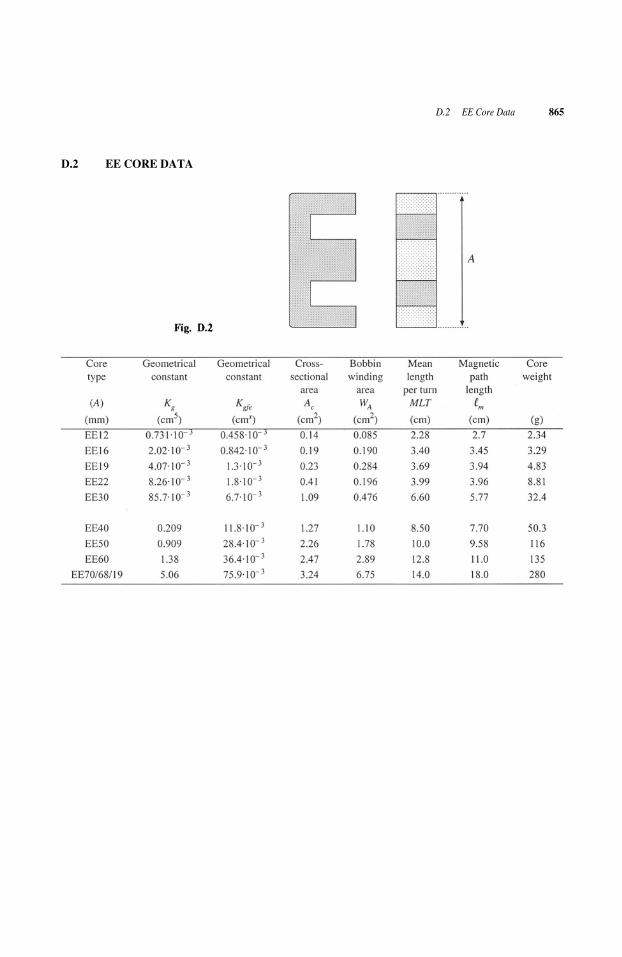
D.2 EE Core Data 865
D.2 EE CORE DATA

866 Magnetics Design Tables
D.3 EC CORE DATA
D.4 ETD CORE DATA

D.5 PQ Core Data 867
D.5 PQ CORE DATA
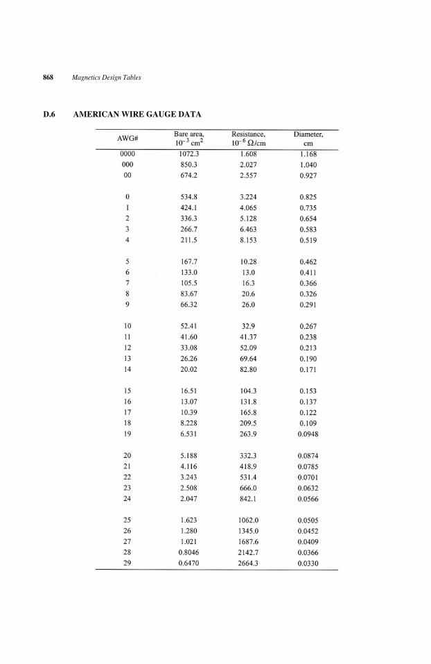
868 Magnetics Design Tables
D.6 AMERICAN WIRE GAUGE DATA

References 869
REFERENCES
C. W. T. MCLYMAN, Transformer and Inductor Design Handbook, Second edition, New York: MarcelDekker, 1988.
Ferrite Materials and Components Catalog, Philips Components.
[1]
[2]

Index
Air gapin coupled inductor, 529, 551, 553in flyback transformer, 530,559in inductor, 499-501, 525-526, 539-542, 544in transformer, 504(mH/1000 turns), 545
American wire gauge (AWG)data, 868-869design examples, 557, 560, 575, 580
Amorphous alloys, 507Ampere’s law, 493-494Amp-second balance (see Capacitor charge balance)Apparent power, 598Artificial ramp
circuit, 446effect on CPM boost low-harmonic rectifier, 654-
656effect on line-to-output transfer function of CCM
buck, 466-469effect on small-signal CCM models, 459-466effect on small-signal DCM models, 473-480effect on stability of CPM controllers, 444-449
Asymptotes (see Bode plots)Audiosusceptibility (see Line-to-output transfer
function)Average current control
feedforward, 650-652in low-harmonic rectifier systems, 648-654modeling of, 652-654
Averaged switch modeling, 226-247of current-programmed CCM converters, 454-459of current-programmed DCM converters, 473-480in discontinuous conduction mode, 410-431equivalent circuit modeling of conduction losses,
242-244, 816-818
equivalent circuit modeling of switching losses,244-247
examplesnonideal buck converter, 244-247nonideal buck-boost converter, 242-244CCM SEPIC, 228-235
of ideal CCM switch networks, 226-241, 815-816,822-825
of ideal DCM switch networks, 416, 822-825of quasi-resonant converters, 768-790
Average powerand Fourier series, 590-593modeled by power source element, 414-418, 454-
459, 473-480in nonsinusoidal systems, 590-603predicted by averaged models, 56power factor, 594-598sinusoidal phasor diagram, 598-599
Averagingapproximation, discussion of, 189-190, 194-196averaged switch modeling, 226-247basic approach, 192-204capacitor charge balance, 21-22circuit, 226-247to f ind dc component, 5, 14flyback ac model, 209-218inductor volt-second balance, 20-21introduction to, 187-192modeling efficiency and loss via, 56to model rectifier output, 668-670to model 3ø converters, 685-690of quasi-resonant converters, 768-790state-space, 213-226
Ballast, electronic 705-707

872 Index
resonant inverter design, 726-740Battery charger, 8, 70B-H loop
in an ac inductor, 527-528in a conventional transformer, 148, 528in a coupled inductor, 529-530in a f i l t e r inductor, 526-527in a flyback transformer, 530-531modeling of, 494-495
Bidirectional dc–dc converters, 70Bipolar junction transistor (BJT)
breakdown mechanisms in, 85-86construction and operation of, 81-86current crowding, 84-85Darlington-connected, 86idealized switch characteristics, 65-66on resistance, 52, 81-82quasi-saturation, 82, 85storage time, 84stored minority charge in, 81-85sw i tch ing waveforms, 82-84
Bode plots (see also Harmonic trap filters, Sinusoidalapproximation)asymptote analytical equations, 281CCM buck-boost example, 294-299combinations, 278-281complex poles, 282-286frequency inversion, 277-278graphical construction of, 302-317
addition, 303-307closed-loop transfer funct ions, 337-340division, 311-313parallel combination, 308-310parallel resonance, 309-310series resonance, 305-307
impedance graph paper, 310nonm in imum phase zero, 276reactance graph paper, 310real pole, 269-274real zero, 275RHP zero, 276transfer functions of buck, boost, buck-boost, 300
Body diode (see MOSFET)Boost converter (see also Bridge configuration, Push-
pull isolated converters)active switch ut i l izat ion in, 173, 676averaged switch model, DCM, 419-420circuit-averaged model, 235-239current-programmed
averaged switch model, CCM, 455-456averaged switch model, DCM, 477small-signal ac model, CCM, 458-459, 460-463,
469-470small-signal ac model, DCM, 478-480
as inverted buck converter, 132-133as low-harmonic rectifier, 642-646, 648-663, 666,
674-685, 832-834nonideal analysis of, 42-49, 52-56quasi-resonant ZCS, 778-779s imulat ion example, 832-834small-signal ac model
CCM, 204-205, 252-253DCM, 424-429
steady-state analysis of,CCM, 22-27DCM, 117-124
transfer functions, CCM, 300Bridge configuration (dc–dc converters)
boost-derived ful l bridge, 165-166buck-derived fu l l bridge, 149-152buck-derived half bridge, 152-154ful l bridge transformer design example, 576-580m in im izat ion of transformer copper loss in, 549-550
Bridge conf igurat ion (inverters)single phase, 7-8, 138-141, 143-145three phase, 70, 141-143
Buck-boost converter (see also Flyback converter)averaged switch model, DCM, 410-420as cascaded buck and boost converters, 134-136current-programmed
averaged switch model, DCM, 473-477more accurate model, CCM, 461-463simple model, CCM, 450-454small-signal ac model, DCM, 478-480
dc–3øac inverter, 71-72DCM characteristics, 112, 124-125, 420as low-harmonic rectifier, 645-646, 650man ipulat ion of ac model into canonical form, 250-
252nonideal, state-space averaged model of, 221-226non invert ing version, 135, 143-144as rotated three-terminal cell, 137s imulat ion of, 819-822small-signal ac model, CCM, 204-205, 252-253small-signal ac model, DCM, 420-425transfer functions, CCM, 294-300transformer isolation in, 161-165
Buck converter (see also Bridge configuration, Forwardconverter, Push-pull isolated converters), 5-6, 13-22,31-33active switch utilization in, 173averaged switch model, 239-241current-programmed
averaged switch model, CCM, 454-457

873
averaged switch model, DCM, 477-478small-signal ac model, CCM, 453, 462, 466-470small-signal ac model, DCM, 477-480
equivalent circuit modeling of,small-signal ac, CCM, 204-205, 253small-signal ac, DCM, 424-426steady-state, CCM, 50-52steady-state, DCM, 420
as high power factor rectifier, 646multi-resonant realization, 784-786quasi-square-wave resonant realizations, 787-790quasi-resonant realizations
zero current switching, 708, 768-782zero voltage switching, 783-784
simulation examplescurrent programmed control, 837-839voltage regulator, 827-831
small-signal ac modelCCM, 204-205, 253DCM, 424-427
steady-state analysis of,CCM, 13-22, 31-33, 50-52DCM, 111-117, 418-420
switching loss in, 93-100, 244-247employing synchronous rectifier, 73-74transfer functions, CCM, 300
converter, 145-146Buck 3ø inverter (see Voltage source inverter)
Canonical circuit model, 248-253manipulation into canonical form, 250-253parameters for buck, boost, buck-boost, 253physical development of, 248-250transfer functions predicted by, 248-250
Capacitor amp-second balance (see Capacitor chargebalance)
Capacitor charge balanceboost converter example, 24-25
converter example, 29-30definition, 22in discontinuous conduction mode, 115nonideal boost converter examples, 44, 54
Capacitor voltage rippleboost converter example, 26-27buck converter example, 31-33in converters containing two-pole filters, 31-33
converter example, 30-31Cascade connection of converters, 134-137Characteristic value (current programmed mode),
445, 448Charge balance (see Capacitor charge balance)Circuit averaging (see also Averaged switch modeling),
226-247averaging step, 229-231examples
buck, 239-241boost, 235-239SEPIC, 228-234
linearization, 232-235obtaining a time-invariant network, 228-229summary of, 226-227
Commutationfailure, 621notching, 622in 3ø phase controlled rectifier, 620-622
Compensators (see also Control system design)design example, 354-362, 827-831lag, 351-353lead, 348-351, 358-359PD, 348-351, 358-359PI, 351-353PID, 353-354, 359-362
Complex power, 598, 620Computer power supply, 7-8Computer spreadsheet, design using, 174-176Conduction loss (see Copper loss, Semiconductor con-
duction loss)Conductivity modulation, 74-76, 78, 82, 83, 87, 89Control system design (see also Compensators, Nega-
tive feedback), 331-376compensation, 348-354construction of closed-loop transfer functions, 334-
340design example, 354-362, 827-831for low-harmonic rectifiers
approaches, 648-663, 668-673modeling, 652-653, 668-673
phase margintest, 341-342vs. closed-loop damping factor, 342-345
stability, 340-347voltage regulator
block diagram, 332-333, 336, 355-357design specifications, 347-348
Control-to-output transfer functionas predicted by canonical model, 248-250of CCM buck, boost, and buck-boost converters, 300of current programmed converters, 453, 458-459,
464-472, 480of DCM converters, 426-427, 433input filter, effect on, 380-382
Conversion ratio M (see also Switch conversion ratioof boost, 16, 24, 123, 420of buck, 16, 116-117, 420

874 Index
of buck-boost, 16, 124, 420of converter, 29-30, 420of loss-free resistor networks, 416-418in low-harmonic rectifiers, 641-642modeling of, 39-42of quasi-resonant converters, 762, 770, 778of parallel resonant converter, 719-721, 748-752of SEPIC, 146, 420of series resonant converter, 716-718, 740-748via sinusoidal approximation, 714-715
Copper lossallocation of window area to minimize, 545-550,
567-568high frequency effects
skin effect, 508-510proximity effect, 510-525
inductor design to meet specified, 539-545low frequency, 508modeling in converters, 43-53multiple winding design to meet specified, 545-554
Core loss, 506-507, 527-529, 560-562, 565-567Correction factor (see also Extra element theorem),
384, 844, 849Coupled inductors, 529-530, 545, 550-554
in converter, 534-535, 529design of, 545-554in multiple-output buck-derived converters, 529-
530, 554-557Crossover frequency, 338-346
converteractive switch utilization of, 173as cascaded boost and buck converters, 136-137conversion ratio M(D), 30, 420DCM averaged switch model of, 418-420as low-harmonic rectifier, 645-646, 650, 676as rotated three-terminal cell, 136-137steady-state analysis of, 27-31transformer design example, 573-576with transformer isolation, 170-171
Current-fed bridge, 144-145Current injection, 367-368Current programmed control, 439-487
ac modeling ofvia averaged switch modeling, CCM, 454-459via averaged switch modeling, DCM, 473-480CCM more accurate model, 459-473CCM simple approximation, 449-459
artificial ramp, 445-449controller circuit, 440, 446controller small-signal block diagram, 459-464in full-bridge buck converters, 152in half-bridge buck converters, 154, 441
in low harmonic rectifiers, 654-656oscillation for D > 0.5, 441-449in push-pull buck converters, 160, 441
Current ripple (see inductor current ripple)Current sense circuit, isolated, 181-182Current source inverter (CSI), 142-143Cycloconverter, 1, 72-73
Damping (see also Q-factor, Input filters)factorof input filters, 380, 385-392optimal, 392-398vs. overshoot, 346-347
DC conversion ratio (see Conversion ratio M)DC l ink, 8-9DC transformer model
in averaged switch models, 232-235, 237-241, 247in canonical model, 248-253comparison w i th DCM model, 410derivation of, 40-42equivalence with dependent sources, 40manipulation of circuits containing, 41-42, 47-48in a nonideal boost converter, 47-48, 55in a nonideal buck converter, 51in small-signal ac CCM models, 204-205, 212-213
Decibel, 267-268Delta-wye transformer connection, 628-629Dependent power source (see Power source element)Derating factor, 174Design-oriented analysis, techniques of
analyt ical expressions for asymptotes, 281approximate factorization, 289-293doing algebra on the graph, 302-317extra element theorem, 843-861frequency inversion, 277-278graphical construction
of Bode plots, 302-317of closed-loop transfer functions, 337-340
input filter design inequalities, 381-385, 392, 399load-dependent properties of resonant inverters,
726-740low Q approximation, 287-289philosophy of, 267, 302-303
Differential connection of loadpolyphase inverter, 141-143single-phase inverter, 138-141
Diodeantiparallel, 67characteristics of, 77fast recovery, 77forward voltage drop (see also Semiconductor con-
duction losses), 52-55, 77

875
freewheeling, 67parallel operation of, 77recovered charge 76-77, 96-98, 722, 763-764,
781recovery mechanisms, 76-77, 96-98Schottky, 74, 77, 99soft recovery, 97-98snubbing of, 97, 99, 764-765switching loss, 96-100, 763-765switching waveforms, 76-77, 97, 100, 763-765zero current switching of, 764, 783zero voltage switching of, 722-724, 781, 784-785,
787Discontinuous conduction mode (DCM)
B-H loop, effect on, 530-531boost converter example, 117-124buck converter example, 108-117buck-boost converter example, 410-418in current programmed converters, 473-480equivalent circuit modeling of, 409-420, 473-477in forward converter, 158in line-commutated rectifiers, 611-614, 616-617in low-harmonic rectifiers
boost rectifier, 643-646, 832-834flyback rectifier, 646-648
mode boundaryin boost rectifier, 643-646vs. K, 110-112, 118-119, 123-124vs. load current and 418origin of, 108-112
in parallel resonant converter, 749-752in PWM converters, 107-130, 409-437, 473-480in series resonant converter, 741-748small-signal ac modeling of, 420-433
Displacement factor, 596, 599Distortion factor (see also Total harmonic distortion),
596-597of single-phase rectifier, 596, 610-613
Distributed power system, 7Doing algebra on the graph (see Graphical construction
of Bode plots)Duty ratio
complement of, 14definition of, 14
EC core data, 866Eddy currents
in magnetic cores, 506in winding conductors, 508-511
EE core data, 865Effective resistance
in DCM averaged switch model, 413-420
in loss-free resistor model, 413-420in resonant converter models
with capacitive filter network, 711-713with inductive filter network, 718-720
Emulated resistance 638-640Efficiency, 2
averaged switch modeling, predicted by, 247of boost converter
as low-harmonic rectifier, 683-685nonideal dc–dc, 48-49, 55
calculation via averaged model, 48-49, 55vs. switching frequency, 100-101
Equivalent circuit modelingby canonical c ircu i t model, 247-253of CCM converters operating in steady-state, 39-61of converters having pulsating input currents, 50-52of current programmed switch networks
CCM, 454-459DCM, 473-480small-signal models, 452-453, 457-459, 478-480
of flyback converter, CCM, 165, 212-213of ideal rectifiers, 638-640, 658-686of ideal dc–dc converters, 39-41of inductor copper loss, 42-52small-signal models, construction of
CCM, 201-203, 211-213, 225-226DCM, 420-433current programmed, 452-453, 457-459, 478-480
of switching loss, 246-247of switch networks
CCM, 235-241DCM, 410-420
of systems containing ideal rectifiers, 666Equilibrium (see Steady state)Equivalent series resistance (esr) of capacitor, 602-603ETD core data, 866Evaluation and design of converters, 171-176Experimental techniques
measurement of impedances, 318-321measurement of loop gains
by current injection, 367-368by voltage injection, 364-367of an unstable system, 368
measurement of small-signal transfer functions,317-318
Extra element theorem, 843-861applications of
input filter design, 381-392, 398-399, 857-859transfer function, solving for, 850-855unmodeled element, effects of, 855-857resonant inverter, load dependence of, 731, 859-
861

876 Index
basic result, 843-846correction factor, 384, 844, 849
deviation caused by, 850-852derivation, 846-849impedance inequalities, 849-850nulling, 845-846reciprocity relationship, 736, 845
driving-point impedance, 845impedance, 845-846
Factorization, approximateapproximate roots of arbitrary-degree polynomial,
289-293graphical construction of Bode diagrams, 302-317low-Q approximation, 287-289
Faraday’s law, 492-493Feedback (see Control system design, Negative feed-
back)Ferrite
applications of, 528, 556, 557, 574, 577core loss, 506-507, 527-529, 566core tables, 863-867saturation flux density, 495, 503, 507, 527
Fill factor (see )Filter design (see Input filter design)Filter inductor
B–H loop of, 527design of
derivation of procedure, 539-544step-by-step procedure, 544-545
Flux , 492Flux density B
definition, 492saturation value , 495
Flux-linkage balance (see Inductor volt-second bal-ance)
Flyback converter (see also Buck-boost converter)active switch utilization, 171-174derivation of, 161-162nonideal, ac modeling of, 204-213rectifier, 646-648spreadsheet design example, 174-176steady-state analysis of, 161-165two transistor version, 180utilization of flyback transformer, 165
Flyback transformer, 522, 530-531, 552design example, 557-562
Forced commutation of SCRs, 89-90Forward converter (see also Buck converter), 154-159
active switch utilization, 173spreadsheet design example, 174-176steady-state analysis of, 154-159
transformer reset mechanisms, 157-158transformer utilization in, 159two transistor version, 158-159
Four-quadrant switches (see Switch)Freewheeling diode, 67
Gate turn-off thyristor (GTO), 90Geometrical constant (seeGraphical construction of Bode plots (see also Bode
plots, Design-oriented analysis)of converter transfer functions, 313-317division, 311-313of harmonic trap filters, 622-628parallel combinations, 308-310parallel resonance, 309-310of parallel resonant converter, 720-721series combinations, 303-307series resonance, 305-307of series resonant converter, 715-717
Grounding problems, 319-321Gyrator, 744-745
Harmonic correction, 690-691Harmonic loss factor 523-525Harmonics in power systems
average power vs. Fourier series, 590-593distortion factor, 596harmonic standards, 603-605neutral currents, 599-600power factor, 594-598root-mean-square value of waveform, 593-596rectifier harmonics, 597-598in three-phase systems, 599-603total harmonic distortion, 596
Harmonic trap filters, 622-628bypass resistor, 626-628parallel resonance in, 624-626reactive power in, 628
H–bridge, 7, 139-141, 143-145Hold-up time, 665Hot spot formation, 77, 88Hysteresis loss 506Hysteretic control, 657-659
Ideal rectifier (see also Low harmonic rectifiers)in converter systems, 663-673properties of, 638-640realization of
single phase, 640-648three phase, 687-691
rms values of waveforms in, 673-677single phase, 638-642

877
three phase, 685-687IEC 1000, 603-604IEEE/ANSI standard 519, 604Impedance graph paper, 310Inductor copper loss (see Copper loss)Inductor current ripple
in ac inductor, 527-528boost example, 25-26buck example, 19calculation of, 19in converters containing two-pole filters, 31-33
converter example, 30-31in filter inductor, 525-526magnitude vs DCM, 108-110
Inductor designac inductor design
derivation, 580-581step-by-step procedure, 582-583
filter inductor designderivation, 539-544step-by-step procedure, 544-545
Inductor volt-second balanceboost example, 24buck example, 21
converter example, 28-29definition, 20in discontinuous conduction mode, 112
Input filters, 377-408, 857-859cascaded filter sections, 398-404
noninteraction, impedance inequalities for, 398-399
two-section design example, 400-404conducted EMI, attenuation of, 377-378conducted susceptibility, 378damping of, 391-404
parallel damping, 394, 395-396parallel damping, 394, 396-397series damping, 394, 398
effect on control-to-output transfer functionbuck example, 380, 389-392general result, 381-382negative resistance oscillations, 382-384results for basic converters, 382right half-plane zeroes, 390
impedance inequalities for designconstruction of, buck example, 385-389control-to-output transfer function, to avoid
changing, 384output impedance, to avoid changing, 385
Input port, converterac modeling of, 197boost static characteristics, 643-644, 655-656
modeling of, via state-space averaging, 222, 225-226
steady-state modeling of, 50-52Inrush current, 646, 665, 676Insulated-gate bipolar transistor (IGBT)
construction and operation of, 86-88current tailing in, 87-88, 95-96equivalent circuit, 87forward voltage drop, modeling of, 88idealized switch characteristics, 65-66parallel operation of, 88switching loss in, 95-96, 768
Inversion of source and load, 132-133Inverters, 1
high frequency, 705-709, 727-729, 732-739line commutated, 619single phase, 7, 68-69, 138-141sinusoidal analysis of resonant converters, 709-715,
726-740three phase, 69-72, 141-143
Iron laminations, 495, 507
K, dimensionless parametercritical value 110-112, 116-117, 124and DCM boundary, 110-112, 116-117, 124in line-commutated rectifier analysis, 612-613in steady-state DCM analysis, 117, 123-124core geometrical constant
definition of, 543-544, 863ferrite core tables of, 864-869filter inductor design procedure using, 544-545multiple winding magnetics design using, 545, 552-
554ac core geometrical constant
ac inductor design procedure using, 580-583definition of, 569-570, 863ferrite core tables of, 864-869transformer design using,
derivation, 565-570examples, 573-580step-by-step procedure, 570-573
rectifier dimensionless parameter, 612-613window utilization factor, 542
LCC resonant converterdependence of transistor current on load, 732-733design example, 737-740introduction to, 705-707ZVS/ZCS boundary, 734-737
Lenz’s law, 493, 506, 508, 510Linear ripple approximation (see Small ripple approxi-
mation)

878 Index
Line-to-output transfer functionof the buck, boost, and buck-boost converters in
CCM, 300canonical model, as predicted by, 248closed-loop, 334-335, 339-340control system design of, 347-348, 361-362of current-programmed converters, 454, 464-466,
469-471, 480of DCM converters, 427
Litz wire, 522Loop gain (see also Control system design, Negative
feedback)definition, 335measurement of, 362-368
Loss-free resistor modelaveraged switch model of discontinuous conduction
mode, 413-420ideal rectifier model
single phase, 638-640three phase, 685-686
Low harmonic rectifiers (see also Ideal rectifiers)controller schemes
average current control, 648-654current programmed control, 654-656critical conduction mode, 657-659feedforward, 650-652hysteretic control, 657-659nonlinear carrier control, 659-663
modeling ofefficiency and losses, 678-685low-bandwidth control loop, 668-673wide-bandwidth average current control loop,
652-654rms calculations in, 673-678
Low Q approximation, 287-289
Magnetic circuits, 498-501Magnetic field H, 491-492Magnetic path length
definition, 497ferrite core tables, 864-867
Magnetics, 489-586ac inductor design, 580-583basic relationships, 491-498copper loss, 42-45, 508, 510-525core loss, 42, 506-508, 561-562coupled inductor design, 550-557ferrite core tables, 864-867flyback transformer design, 557-562inductor design, 539-562inductor design, multiple winding, 550-562magnetic circuits, 498-501
magnetic devices, types of, 525-531optimizing to m in im ize total loss, 569-570optimizing window allocation to minimize copper
loss, 545-550proximity effect, 508-525transformer basics, 146-149, 501-505transformer design, 565-583
Magnetizing current, 147-148, 502-504Magnetomotive force (MMF)
definition, 491-492magnetic circuit, in, 498-499MMF diagrams, 512-514
Majority carrier devices (see also MOSFET, Schottkydiode), 74-75
Matr ix converter, 72-73Meal length per turn (MLT)
definition, 543ferrite core tables, 864-867
Measurement of transfer functions and loop gains (seeExperimental techniques)
Middlebrook’s extra element theorem (see Extra ele-ment theorem)
Minority carrier devices (see also Bipolar junction tran-sistor, Diode, Gate turn-off thyristor, Insulated-gatebipolar transistor, MOS-controlled thyristor, Siliconcontrolled rectifier), 74-75
Modulation index, 689-690MOS-controlled thyristor (MCT), 91-92MOSFET
body diode, 67-68, 78-79conduction loss, modeling of, 52-56, 204-213, 816-
819construction and operation of, 78-81on resistance, 52-56, 78-81switching loss owing to 98-99, 765-768as synchronous rectifier, 73-74terminal capacitances, 80-81typical characteristics, 80-81zero-voltage and zero-current switching of, 721-726,
765-768Motor drive system, 8-9
Mult iply ing controller (see also Average current con-trol, Current programmed control), 648-659
Multi-resonant switch, 784-786
Negative feedback (see also Control system design)effects of, on network transfer functions, 334-337objectives of, 187, 331-334reduction of disturbances by, 335-337reduction of sensitivity to variations in forward gain
by, 337Nonlinear carrier control, 659-663

879
Nonminimum-phase zero (see Right half-plane zero)
Output characteristicsof the parallel resonant converter, 750of resonant inverters, 727-729of the series resonant converter, 747-748
Overshoot, 346-347, 348
Parallel resonant converteranalysis via sinusoidal approximation, 718-721dependence of transistor current on load, 730-731exact characteristics
continuous conduction mode, 748-751control plane, 751discontinuous conduction mode, 749-751output plane, 750
introduction to, 705-706Permeability
definition, 494-495of free space, 494relative, , 495
Phase asymptotesof complex poles, 284-285inverted forms, 278of real pole, 272-274of real zero, 275of RHP zero, 276
Phase controlof resonant converters, 705of three-phase rectifiers, 617-622of zero-voltage transition dc–dc converter, 791-794
Phase marginvs. closed-loop damping factor, 342-346input filter, undamped, effect on, 390-391stability test, 341-342
Polescomplex, Bode plots of, 282-286the low Q approximation, 287-289real, Bode plots of, 269-274
Pot core data, 864Powdered iron, 495, 507Power factor (see also Total harmonic distortion, Dis-
placement factor, Distortion factor)definition of, 594-598of bridge rectifier, single phase, 597, 610-613of peak detection rectifier, 597of phase-controlled rectifier, three phase, 616, 619-
620Power sink element (see Power source element)Power source element
in averaged switch modelscurrent programmed mode, CCM, 454-457
current programmed mode, DCM, 475-477discontinuous conduction mode, 414-420
definition of, 415-416in ideal rectifier model, 638-640, 646-647, 650, 666,
668-670, 686linearization of, 383-384, 423-424, 457, 668-671in loss-free resistor model, 416-417, 639-640properties of, 415-416in switched-mode regulators, 383-384, 455, 665-666
PQ core data, 867Proximity effect
conductor spacing factor 515interleaving, effect on, 520-522layer copper loss, 515-517Litz wire, effect of, 522MMF diagrams, 512-514PWM waveform harmonics, 522-525simple explanation, 508-512transformer design procedure, accounting for, 572winding loss, total, 518-520
PSpice (see Simulation)Pulse width modulation (PWM), 4-6
modulator ac model, 253-255operation of modulator, 253-255spectrum of PWM waveform, 188-189
Push-pull isolated convertersbased on boost converter, 167-168based on buck converter, 159-160, 441Watkins-Johnson converter, 167-168
Q factor, 283-286canonical model, predicted by, 300closed-loop, vs. phase margin, 342-346of the CCM buck, boost, and buck-boost converters,
300graphical determination of, 307, 310, 312, 314the low Q approximation, 287-289vs. overshoot, 346-347of parallel resonant circuit, 309-310of series resonant circuit , 305-307
Quasi-resonant converters (see also Multi-resonantswitch, Quasi-square-wave switch)zero-current switching dc–dc
full wave, 779-781half wave, 768-779
zero-voltage switching dc–dc, 783-784Quasi-square-wave converters, 787-790Quasi-static approximation, 653-654Quiescent operating point, 190-191, 198, 2205
Reactance graph paper (see Impedance graph paper)Reactive power

880 Index
definition, 598-599in harmonic trap filters, 628in phase-controlled rectifiers, 619-620
Reciprocity relationship (see also Extra element theo-rem), 736, 845
Rectifiers (see also Ideal rectifiers, Low harmonic recti-fiers), 1energy storage in single-phase, 663-668high quality, 589ideal, 637-640line-commutated
phase control of, 617-622single-phase, 597, 609-615three-phase, 615-617three-phase transformer connections in, 628-630twelve pulse, 628-630
in resonant dc–dc converter, 711-713, 718-719Regulator system (see also Control system design),
187-188, 331-334, 665-666Reluctance, 498Resonance
Bode plots of complex poles, 282-286damping of, 391-398graphical construction examples, 305-313harmonic traps, 622-628the low-Q approximation, 287-289parallel resonant network, 309-310series resonant network, 305-307
Resonant converters (see also Quasi-resonant convert-ers, Multi-resonant converters, Quasi-square-waveconverters, Zero voltage transition converter), 705-752analysis of, via sinusoidal approximation, 709-713LCC, 705-706, 731-733, 737-740parallel, 705-706, 718-722, 731, 733resonant link, 707series, 705-707, 709-718, 722-726, 733, 741-748
Resonant inverters, design of, 726-740LCC design example, 737-740output characteristics, 727-729transistor current, dependence on load, 729-733ZVS boundary, dependence on load, 734-737
Resonant link converters, 707Resonant switches (see Quasi-resonant converters,
Multi-resonant switch, Quasi-square-wave convert-ers)
Right half-plane zeroBode plot of, 276caused by input filter, 390physical origins of, 300-302
Ripple, switching, 15-19, 108-110, 188-190Root mean square value
of commonly-observed converter waveforms, 805-812
vs. Fourier series, 593-594of near-ideal rectifier currents, table of, 677of near-ideal rectifier waveforms, 673-678
Rotation of three-terminal cell, 137
Saturationof inductors, 497-498, 501of magnetic materials, 494-495of transformers, 152, 503-504
Schottky diode, 74, 77Semiconductor conduction loss
boost converter example, 52-56inclusion in ac model, 204-213, 221-226, 242-244,
816-822with synchronous rectifier, 73-74
Semiconductor cost, 173-174Semiconductor power devices (see also Bipolar junc-
tion transistor, Diode, Gate turn-off thyristor, Ins-lated-gate bipolar transistor, MOS-controlledthyristor, Schottky diode, Silicon controlled recti-fier), 63-102charge control of, 74, 76, 81-84, 94-95, 99conductivity modulation, 74majority vs. minority carriers, 74realization of switches using, 63-74
SEPIC (see Single-ended primary inductance con-verter)
Series pass regulator, 4Series resonant converter
analysis via sinusoidal approximation, 709-718dependence of transistor current on load, 733exact characteristics
continuous conduction mode, 741-743control plane, 746even discontinuous conduction mode, 744-745odd discontinuous conduction mode, 743-744output plane, 747-748
introduction to, 705-707subharmonic modes in, 717-718zero-current switching in, 722-723zero-voltage switching in, 723-726
Silicon area (see Switch stress)Silicon controlled rectifier (SCR)
construction and characteristics of, 88-92equivalent circuit, 89inverter grade, 90
Silicon steel, 495, 507Simulation, 813-842
ac, 825-827, 829-831, 837-839averaged switch models

881
basic CCM, 815-816CCM with conduction losses, 816-818combined CCM/DCM, 822-825
current programmed control model, 834-837dc, 818-819examples
boost rectifier, 832-834buck-boost transient response, 819-822buck current programmed control, 837-839buck voltage regulator, 827-831SEPIC dc conversion ratio and efficiency, 818-
819SEPIC frequency responses, 825-827
transient, 819-822, 830-831, 833-834Single-ended primary inductance converter (SEPIC),
35-36, 145-146averaged switch model of
continuous conduction mode, 228-233, 825-827discontinuous conduction mode, 418-420, 825-
877conversion ratio M(D) 145-146, 420inverse of, 145-146, 168-171as low-harmonic rectifier, 645, 676-677simulation of, 818-819, 825-827transformer isolation in, 168-171
Single quadrant switchdefinitions, 63-64implementation, 65-67origins of DCM, 107-112
Sinusoidal approximation, 709-713Sinusoidal PWM, 689-690Skin effect (see also Proximity effect), 508-510Slope compensation (see Artificial ramp)Small ripple approximation (see also Averaging)
in ac modeling approach, 192-193, 218-219and average power loss, prediction of, 55-56boost example, 22-27buck example, 17-18
converter example, 27-31definition, 15-17in discontinuous conduction mode, 112-114failure of, in two-pole filters, 31-33
Small-signal ac modelingvia averaged switch modeling, 226-247, 410-433,
454-459via circuit averaging, 226-235of CCM converters, 187-264of current programmed converters, 449-480of DCM converters, 420-433of low harmonic rectifiers, 668-673via state-space averaging, 213-226
Snubber networks, 85, 92, 97, 764-765, 767
Soft switching (see also Zero current switching, Zerovoltage switching), 761-802
Spacecraft power system, 8Spice (see Simulation)Spreadsheet design of converters, 174-176State equations of a network, 213-216State-space averaging, 213-226
discussion, 217-221example: nonideal buck-boost converter, 221-226summary of result, 216-217
Steady stateinductor current waveform, 18-22operating point, 190-191, 198, 217
Subharmonicmodes of series resonant converter, 717-718number 740-741
Switchaveraged modeling of, 226-247, 410-431, 454-459current-bidirectional two-quadrant, 67-70four-quadrant, 72-73ideal SPDT in converters, 4-7, 13-14, 16, 22, 27ideal SPST, 63-64passive vs. active, 65, 90power dissipated by ideal, 5, 14quasi-resonant, 781-790realization of, using semiconductor devices, 63-74single-quadrant, 65-67synchronous rectifier, 73-74voltage-bidirectional two-quadrant, 71-72
Switch conversion ratioboost converter example, 778-779combined CCM/DCM model, 822-824definition, 770, 823-824of multi-resonant switch, 784-786of quasi-resonant switches
full-wave ZCS, 780-781full-wave ZVS, 783half-wave ZCS, 776-779half-wave ZVS, 783
of quasi-square-wave switches, 787-790Switch network, 227, 235-241
boost, 235-239, 241, 424-425, 816buck, 239-241, 424-425, 454-455, 816general two-switch, 228, 230, 233-235, 241, 410-
411, 416, 473-474, 815Switched mode, 3-7Switching frequency
converter efficiency vs., 100-101definition of, 14transformer size vs., 576
Switching harmonics (see also Ripple, switching), 5-6removal of via averaging, 188-190

882 Index
Switching loss (see also Soft switching, Zero currentswitching, Zero voltage switching)averaged switch modeling of, 244-248with clamped inductive load, 93-96and current tailing, 94-96, 768and device capacitances, 98-100, 766and diode recovered charge, 96-97, 99-100, 763-765effect on converter efficiency, 100-101and r ing ing waveforms, 98-100, 763-767and stray inductances, 98-100, 764, 766-767
Switch stress S, 171-174Switch utilization U, 171-174Synchronous rectifier, 73-74
Temperature risein a converter, 2-3in magnetics, 864
Thyristor (see Gate turn-off thyristor, MOS-controlledthyristor, Silicon controlled rectifier)
Topologies of converters (see also Boost, Bridge con-figuration, Buck, Buck-boost, converter, For-ward converter, Transformer-isolated converters,etc.)Cascade connections, 134-137Converter synthesis, 143-146Differential connection of load, 138-143Evaluation and comparison, 171-176, 676-678Inversion of source and load, 132-133Low-harmonic single-phase rectifiers, 640-648Resonant converters, 659-664Resonant switch converters, 781-790Rotation of three-terminal cell, 137Transformer isolation, 146-171
Total harmonic distortion (THD)of current-programmed rectifiers, 655-656definition, 596vs. distortion factor, 596-597IEEE-519 limits, 604-605of peak detection rectifier, 597-598of single-phase bridge rectifiers, 597-598, 610-615of three-phase bridge rectifiers, 615-617, 619
Transfer functions (see also Bode plots)of the buck, boost, and buck-boost converters, 300of current programmed converters, 453-454, 470-
473, 837-839of DCM converters, 427-433, 830graphical construction of, 302-317input filter, effect on, 379-392of low-harmonic rectifiers, 668-673,measurement of, 317-318predicted by canonical model, 248-250, 300simulation of, 825-831, 837-839
Transformer connections in three-phase rectifiers, 628-630
Transformer-isolated converters, 146-171boost-derived topologies, 165-168
converter, 170-171evaluation and comparison of, 171-176flyback, 161-165forward, 154-159ful l bridge buck-derived, 149-152half-bridge buck-derived, 152-154mult iple outputs and cross regulation, 147push-pull buck-derived, 159-160SEPIC, 168-169transformer model, 147-149, 501-505use of volt-second balance in, 148-149, 151-152
TransformersB-H loop in, 148, 503, 528design of,
derivation of procedure, 565-570examples, 573-580step-by-step procedure, 570-573w ind ing area optimization, 545-550
flyback transformer, 161-165leakage inductance, 149, 504-505magnetizing inductance, 147-149, 502-504modeling of, 147-149, 501-505SEPIC transformer, 168-169volt-second balance in, 148-149, 151-152
Triplen harmonicsin three-phase four-wire networks, 600-601in three-phase inverter modulation schemes, 690in three-phase rectifier circuits, 615-616in three-phase three-wire networks, 601
Twelve-pulse rectifier, 629-630Two-quadrant switches (see Switch)
Universal-input rectifiers, 665
Variable-speed ac drive, 8-9Voltage conversion ratio (see Conversion ratio M)Voltage injection, 364-367Voltage-source inverter, 70, 142-143Volt-second balance (see Inductor volt-second balance)
Watkins-Johnson converter, 145, 167-168inverse of, 145isolated push-pull, 167-168
Window areaallocation of, to m in im ize total copper loss, 545-550definition, 542ferrite core tables, 863-867
Window utilization factor 542

883
Wire areainductor design, 542, 545American wire gauge (AWG) table, 868-869
Zero-current switching (ZCS), 708in quasi-resonant converters, 777-778in quasi-square-wave converters, 787in series resonant converter, 722-723ZCS/ZVS boundary, 734-737
Zero-voltage switching (ZVS), 708in active clamp snubber, 794-796in auxiliary resonant commutated pole, 796-797design of LCC resonant converter to attain, 739of diodes, 763-765of IGBTs, 768in LCC resonant converter, 734-737of MOSFETs, 765-768in multi-resonant converters, 784-786in quasi-resonant converters, 783in quasi-square-wave converters, 787-790in series resonant converter, 723-726in zero-voltage transition converter, 791-794ZVS/ZCS boundary, 734-737
Zero-voltage transition buck-derived converter, 791-794