baby peas (pulse early alarm sensor)
TRANSCRIPT

BABY PEAS (Pulse Early Alarm Sensor) A non-evasive vital monitoring system providing caretakers power to make data-driven
decisions for an infant’s wellbeing.
Department of Electrical Engineering and Computer Science
University of Central Florida
Dr. Samuel Richie
Senior Design
GROUP 4 Christopher Ramirez 407-310-0830 [email protected]
Xin Tong 407-4378604 [email protected]
Yowwu Lin 407-435-7804 [email protected]
Benjamin Goolsby 904-347-7935 [email protected]

I
TABLE OF CONTENTS
1 Executive Summary .................................................................................................... 1
2 Project Description ..................................................................................................... 2
2.1 Project Motivation and Goals ............................................................................. 2
2.2 Objectives ........................................................................................................... 2
2.3 Project Requirements and Specifications............................................................ 2
3 Research Related to Project ........................................................................................ 3
3.1 Existing or Similar Project and Products ............................................................ 3
3.1.1 www.owletcare.com ..................................................................................... 3
3.1.2 KnightTime ................................................................................................... 4
3.1.3 Current Majority Market Share Monitors ..................................................... 4
3.2 Relevant Technologies ........................................................................................ 5
3.2.1 Medical ......................................................................................................... 5
3.2.1.1 Infant Sleep Cycles ................................................................................ 5
3.2.1.2 SIDS....................................................................................................... 6
3.2.1.3 Vital Signs ............................................................................................. 7
3.2.1.3.1 Skin Temperature ................................................................................. 7
3.2.1.3.2 Blood Oxygen Levels .......................................................................... 8
3.2.1.3.3 Heart Rate ............................................................................................ 9
3.2.1.3.4 Breathing Rate ................................................................................... 10
3.2.2 Pulse Oximetry Sensors .............................................................................. 11
3.2.3 Temperature Sensors ................................................................................... 13
3.2.4 Body Position Sensors ................................................................................ 14
3.2.4.1 Accelerometers .................................................................................... 15
3.2.4.2 Gyroscopes .......................................................................................... 16
3.2.4.3 IMU ..................................................................................................... 16
3.2.5 Wireless Technology .................................................................................. 16
3.2.5.1 Bluetooth ............................................................................................. 17
3.2.5.1.1 Bluetooth Classic............................................................................. 17
3.2.5.1.2 Bluetooth Low Energy .................................................................... 17
3.2.5.2 WIFI..................................................................................................... 18
3.2.5.3 ZIGBEE ............................................................................................... 19
3.2.5.4 ANT/ANT+ ......................................................................................... 19
3.2.5.5 Zwave .................................................................................................. 20

II
3.2.6 Data Communications ................................................................................. 20
3.2.6.1 I2C ........................................................................................................ 21
3.2.6.2 SPI ....................................................................................................... 21
3.2.6.3 UART .................................................................................................. 21
3.2.7 Mobile Applications.................................................................................... 21
3.2.7.1 IOS ....................................................................................................... 21
3.2.7.2 Windows Phone ................................................................................... 21
3.2.7.3 Android ................................................................................................ 22
3.2.8 Microcontroller / FPGA .............................................................................. 22
3.2.9 Power .......................................................................................................... 22
3.2.9.1 Power Considerations and Safety ........................................................ 22
3.2.9.1.1 Safety ............................................................................................... 23
3.2.9.1.2 Operation ......................................................................................... 25
3.2.9.1.3 Interference Considerations............................................................. 25
3.2.9.1.4 Electrostatic Discharge Protection .................................................. 27
3.2.9.2 AC Power ............................................................................................ 28
3.2.9.3 DC Power ............................................................................................ 28
3.2.9.3.1 Solar Power ..................................................................................... 28
3.3 Strategic Components ....................................................................................... 31
3.3.1 Pulse Oximeter Sensor AFE4490 ............................................................... 31
3.3.1.1 Analog Pins.......................................................................................... 32
3.3.1.2 Digital Pins .......................................................................................... 32
3.3.1.3 Supply Pins .......................................................................................... 33
3.3.1.4 Communication Pins............................................................................ 33
3.3.1.5 Reference Pins ..................................................................................... 33
3.3.2 Alternative Design of Analog Front End Pulse Oximeter .......................... 34
3.3.3 Photo Diodes/Photo Diode Sensor .............................................................. 36
3.3.4 Body Position Sensor .................................................................................. 36
3.3.4.1 Invensense MPU-60x0 series .............................................................. 37
3.3.4.2 Analog Device ADXL362 ................................................................... 38
3.3.4.3 Freescale Semiconductor MMA8451Q ............................................... 39
3.3.5 Skin Temperature Sensor ............................................................................ 41
3.3.5.1 TMP006 ............................................................................................... 41
3.3.5.2 TMP103 ............................................................................................... 46
III
3.3.6 Communications Sensor ............................................................................. 47
3.3.6.1 CC2541 BLE SOC............................................................................... 48
3.3.6.2 CC2564-PAN1326............................................................................... 49
3.3.6.3 nRF51822 BLE Module ...................................................................... 50
3.3.7 Microcontroller ........................................................................................... 53
3.3.7.1 TI MSP430 FRAM Series ................................................................... 53
3.3.7.2 ATMEL ............................................................................................... 53
3.3.7.3 PIC(MICRO) ....................................................................................... 54
3.3.7.4 CC2541 ................................................................................................ 54
3.3.7.5 MSC1210 ............................................................................................. 55
3.3.8 Power Supply .............................................................................................. 55
3.3.8.1 Battery ................................................................................................. 55
3.3.8.2 AC power supply ................................................................................. 56
3.3.8.3 DC power supply ................................................................................. 56
3.3.8.3.1 USB ................................................................................................. 56
3.3.8.3.2 Solar ................................................................................................ 57
3.3.8.4 Board supply Regulator ....................................................................... 57
3.3.8.4.1 Linear Regulators Linear Tech LT1761 .......................................... 57
3.3.8.4.2 Switching Regulators Texas Instruments TPS62740 ...................... 59
3.3.8.4.2.1 Pin Functions ....................................................................................... 63
3.3.8.5 Requirements ....................................................................................... 70
3.3.8.6 Schematics for TPS62740 ................................................................... 71
4 Project Hardware and Software Design Details ....................................................... 74
4.1 Hardware ........................................................................................................... 74
4.1.1 Pulse Oximeter Sensor Design.................................................................... 75
4.1.2 Body Position Sensor Design...................................................................... 76
4.1.3 Skin Temperature Sensor Design................................................................ 77
4.1.4 Communications / Microcontroller Design ................................................ 79
4.1.4.1 Communications .................................................................................. 79
4.1.4.2 Microcontroller CC2541 Design characteristics ................................. 81
4.1.4.2.1 Electrical Characteristics ................................................................. 81
4.1.4.2.2 Current Consumption with TPS62730 ............................................ 81
4.1.4.2.3 General Characteristics ................................................................... 82
4.1.4.3 CC2541 Block Diagram ...................................................................... 82

IV
4.1.4.4 CPU and Memory ................................................................................ 82
4.1.4.5 Peripherals ........................................................................................... 83
4.1.4.6 Application information CC2541 ........................................................ 86
4.1.4.6.1 Power configuration ........................................................................ 86
4.1.4.6.2 SPI bus AC Characteristics of CC2541........................................... 87
4.1.4.6.3 I2C of CC2541 ................................................................................. 90
4.1.4.6.4 8051 CPU ........................................................................................ 91
4.1.4.6.4.1 Serial Data Input/Output ..................................................................... 92
4.1.4.7 Microcontroller Coding Software ........................................................ 94
4.1.4.8 Debugging Feature CC2541 ................................................................ 98
4.1.4.9 CC2541 debug device ........................................................................ 100
4.1.5 User Interface Design ............................................................................... 101
4.1.5.1 Touchscreen ....................................................................................... 102
4.1.5.1.1 Resistive Touch ............................................................................. 102
4.1.5.1.2 Capacitive Touch........................................................................... 104
4.1.5.1.3 Touch Screen kits .......................................................................... 104
4.1.5.2 Software Development ...................................................................... 104
4.1.5.3 Software diagrams ............................................................................. 105
4.1.5.4 Class diagram .................................................................................... 106
4.1.6 Bluetooth Handshake ................................................................................ 106
4.1.6.1 Android Platform for Classic Bluetooth ............................................ 106
4.1.6.1.1 Setting up the Bluetooth device: ................................................... 107
4.1.6.1.2 Searching for other devices: .......................................................... 107
4.1.6.1.3 Connecting device as server-side: ................................................. 108
4.1.6.1.4 Managing a connection: ................................................................ 110
4.1.6.1.5 Profiles: ......................................................................................... 110
5 Project Prototype Construction and Coding ........................................................... 110
5.1 Parts Acquisition and BOM ............................................................................ 110
5.1.1 Part Vendors.............................................................................................. 110
5.1.2 Newark ...................................................................................................... 110
5.1.2.1 Digikey .............................................................................................. 110
5.1.2.2 Sparkfun and local hobby centers ...................................................... 111
5.1.2.3 Price list of Hardware “BOM” / Development Tools........................ 111
5.2 PCB Vendor and Assembly ............................................................................ 112

V
5.2.1 PCB Vendors ............................................................................................ 112
5.2.1.1 4PCB .................................................................................................. 112
5.2.1.2 PCB Fabexpress ................................................................................. 112
5.2.1.3 Custom Circuit Boards ...................................................................... 112
5.2.2 PCB Assembly Houses ............................................................................. 113
5.2.2.1 QMS (Quality Manufacturing Solutions) .......................................... 113
5.2.2.2 Conilec ............................................................................................... 113
5.2.2.3 DIY (Do it yourself) .......................................................................... 113
6 Project Prototype Testing ........................................................................................ 114
6.1 Hardware Prototype Testing ........................................................................... 114
6.1.1 Battery, Regulator, and Charging Circuits ................................................ 114
6.1.1.1 Temperature Sensor Hardware .......................................................... 115
6.1.1.2 Body Position Sensor Hardware ........................................................ 116
6.1.1.3 Pulse Oximetry Sensor Hardware...................................................... 116
6.1.2 Wireless Communications Hardware Test................................................ 117
6.2 Software Prototype Testing............................................................................. 118
6.2.1 CC2541 Software Testing ......................................................................... 118
6.2.2 User Interface Module Software Test ....................................................... 119
6.3 System Level Testing ...................................................................................... 120
6.3.1 Skin Temperature Final Test ..................................................................... 120
6.3.2 Body position Final Test ........................................................................... 121
6.3.3 Pulse Oximetry Final Test ........................................................................ 122
6.3.4 Weight, Battery Life, and Wireless Range Final Test .............................. 123
7 Administrative Content ........................................................................................... 124
7.1 Milestones and Schedule Discussion .............................................................. 124
7.2 Roles and Responsibilities .............................................................................. 128
7.3 Budget and Finance Discussion ...................................................................... 129
7.4 Conclusion ...................................................................................................... 129
8 Appendices .............................................................................................................. 130
8.1 Appendix A: References ................................................................................. 130
8.2 Appendix B: Copyright Permissions .............................................................. 134

1
1 Executive Summary
Despite being a successful species at large, humanity starts off life as a weak and wholly
dependent creature, with little capacity for communications or self-awareness. An infant
requires 24 hours of careful supervision; a daunting task in today’s busy world on a good
day and a seemingly impossible task on a normal day. The Baby peas unit seeks to take
some of the burden from the shoulders of the caretaker, giving him or her ability to
multitask and accomplish chores around the house or take a brief moment of watchful
relaxation. While not intended as a fully autonomous baby sitter of sorts, incorporating
Baby peas in daily life will improve the quality of existence for both the infant and the
caretaker.
This document summarizes the thought process behind designing the Baby peas system
in terms of medical background, hardware and software solutions. Section 2 details the
motivations behind the project and lists out the primary objectives. In addition, this
section gives the preliminary parameters for unit operation, including battery life,
physical packaging of device, sensor accuracy targets, wireless transmission range, and
operating temperatures. Section 3 seeks to flesh out the background of the unit in three
categories, existing examples, medical principles, and technological offerings. Starting
off with existing projects similar to the Baby peas unit, primarily the owlet care sock and
the KnightTime project for University of Central Florida’s senior design during Fall 2012
and Spring 2013, the chapter then moves to other market share units, which are
conventional baby monitors offered by such major health care companies like Philips.
The latter half of section 3 investigates the relevant medical understanding underlining
infant health markers and also the technologies involved in monitoring those bio-markers,
such as temperature or pulse-ox sensors. Finally, this segment’s last half ends with
discussions on the choices for communications, mobile applications, the central
microprocessor, and power systems. In this section, all of the chosen strategic
components are listed. Section 4 delves hardware and software design details, including
each sensor chosen, the microcontroller CC2541, the power systems, and mobile
application. In addition to those modules, the discussion includes how data transfers
between each module, and includes serial protocols such as I2C and SPI. Unit 5 lists
companies for printing the designed circuit board, and in addition lists options for
populating the printed board. Once the board is made and populated, section 6
inventories prototype and system level testing. The prototype testing provides a listing of
each sensor test, taking care to isolate each system and targeting each system specifically
before a general integration test. After ensuring the viability, safety precautions and
robustness of the unit, a final test commences on each group member. This document
finishes with chapter 7, a section on general milestones for senior design 2, which is the
next step in building Baby peas, and also the budget finance discussion and the roles and
responsibilities of each member in the group.

2
2 Project Description
2.1 Project Motivation and Goals Markets sell a variety of baby monitoring equipment that includes an abundance of
features; some common features include infrared cameras and ambient temperature
sensor. While many traditional monitors focus on the video as a safety feature, a baby’s
wellbeing is sometimes hard to decipher on a grainy screen. Our product, instead,
focuses on quantifiable bio-markers, such as pulse oximeter, body position, and non-
contact temperature sensors, to indicate the baby’s health. This project strives to improve
upon the current models and involves several factors for specific medical and social
considerations. Geared toward infants and young toddlers, Baby Peas is designed to
provide an empirical picture of the newborn’s physical condition. If the pulse-ox detects
sudden drops in pulse or oxygen levels, a triggered alarm alerts the caretaker. Whereas,
if relying on video observation, the caretaker could find his attention distracted or
misread a picture on the screen and lose critical minutes in a potential serious medical
emergency. In addition to basic pulse functions, the body position and the temperature
sensors can help monitor against risk factors for sudden infant death syndrome (SIDS).
Although no definitive cause is known, the medical community agrees on several factors
that can magnify risk of SIDS. The body position and temperature sensor should mitigate
the risk factors. The main goal is to attach a small device around the ankle of a baby and
secure it in such a way it can read heart rate, oxygen levels, body position, and skin
temperature accurately without harm to the child. Once the data is obtained the ankle
device will transmit data wirelessly to a host device such as a smart phone. At no time
during the project will the ankle device be tried on a child of any age range. The concept
can be proven out on members of the team and then scaled down in the future if so
desired.
2.2 Objectives Due to the nature of usage, form and packaging comprises a large portion of design.
Because the unit is planned to operate under direct contact with the baby, safety
considerations include minimal invasion and heat dissipation. In addition, ergonomic
concerns include ease of use, bulk, and portability. Power factors in as well due to the
targeted length of function time. Primary objectives are wireless transmissions of the bio
marker data to a hand held device which is reliable over a wide range of environmental
conditions and for a specific length of time. This objective goal needs to be reached by
obtaining the bio marker from the ankle of the user. By reaching these objectives all of
the group members will obtain desired knowledge in their respective career interests
which will eventually help out with employment options in the future.
2.3 Project Requirements and Specifications The requirements and specifications of the project can been seen in Table 1. These
specifications are baseline goals to be reached which can be measured against for the
success of the Baby Peas project.

3
Table 1 Specification for the Baby Peas Project
3 Research Related to Project
3.1 Existing or Similar Project and Products
3.1.1 www.owletcare.com
Owlet Baby Monitor was developed by six students from Brigham Young University and
won the first prize of Student Innovator of The Year in 2012. Tanor Hodges, who works
at University of Utah Hospital, came up the idea with his friend Kurt Workman who is a
chemical engineering student. Student Innovator of the Year (SIOY) is a competition for
Brigham Young University for developing and encouraging students with new ideas,
products with technology and engineering. It is sponsored jointly by the Ira A. Fulton
College of Engineering and Technology and the Rollins Center for Entrepreneurship and
Technology at the Marriott School. The sensor is incorporated in the Smart Sock which is
worn by babies. It is capable of measuring heart rate, pulse oximetry, temperature and
body position. The main motivation for the project was to combat SIDS (Sudden Infant
Death Syndrome.) The data collected by the sensors are transmitted to parents’ smart
phones and the cloud which is accessible via any devices with internet connection. The
main transmission method from the portable sensors to the mobile phones is via
Bluetooth 4.0. The battery life is unknown but it is rechargeable. Notifications will be
sent out when the batteries are running low. The Bluetooth is set at 2.4 GHz so that it
would not interference with other cell phones, home alarms, and other electronics. Apple
iPhone application has been developed and released; the developers are currently
working on android counterpart. Upon the product debut, both platforms will be available
to the consumer. The applications can be used with tablets as well. [7]
The notable features on Owlet Baby Monitors:
Washable when the electronics are pulled out from the Smart Sock.
Capable of monitoring more than one child at the same time.
Cloud storage of data.
Crowd funded.
Device Battery Life > 12 hours
Weight of the Device < .5 pounds
Dimensions (Ankle Device) 50 Width x 100 Length x 15 Height mm
Blood Oxygen Level Accuracy +-20%
Heart Rate Accurcy +-20%
Skin Temperature Accuracy +-20%
Position Accuracy Back , Stomach, right side, Left Side
Wireless Transmission Range 100 Feet

4
3.1.2 KnightTime
KnightTime is developed by a group of senior design students from University of Central
Florida in 2013. The group members were Anthony Bharrt who was a computer
engineering major student as well as Facundo Gauna. The rest of the team members are
Ryan Murphy and Bartholomew Straka, both electrical engineering students. The
motivation of the project was to improve the quality of the sleep from data collected by
biomedical sensors. Individuals could utilize the information gathered from the sleep
management system to make decision or adjust personal habits in order to improve the
quality of sleep. The key points measured by the KnightTime system are temperature,
body movement, and heart rate. The wearable product was designed to be comfortable
and non-irritable. Based on the collected data, software algorithms can determine the
sleep stage of the individuals and wake them up once the sleep duration is met. Battery
was crucial on this project because it had to provide the necessary power to the onboard
devices, while maintaining the compact size. The sensors and the peripherals were chosen
with low power consumption as top priority. The main focus for the product was user
friendliness, modularity, and scalability. The user interface was designed to be very user
intuitive. The hardware was simple and easily worn. [11]
The notable features on the KnightTime monitor:
REM monitoring.
Typical usage is for adults.
Privately funded.
3.1.3 Current Majority Market Share Monitors
Various baby monitoring systems are currently available in the market. They can be
categorized by functionalities such as visual, audio, and movement monitoring system.
Most of the monitoring systems do not have any device implemented or attached to the
babies thus they do not require FDA approval. Motorola MBP36 Remote Wireless Video
Baby Monitor uses video camera capable up to 590 feet with infrared night vision. [5] It
uses AC adapter as the main power source for the video/audio device and sends the video
to the parent unit which has rechargeable Ni-MH battery pack. This particular unit also
features two-way audio communication system with automatic channel selection. The
parent unit is a standalone 3.5 inch LCD display with speakers and microphone. The
retail price ranges from $150 to $250 based on additional features availability.
Philips AVENT Baby Monitor has a two-way audio system with guaranteed
uninterrupted connection. [6] The packaging state that it provides crystal clear audio
signal to the paired unit with automatic channel selection. Both the baby and the parent
devices have a rechargeable battery pack with a low-battery warning light. The claimed
operation duration is twenty-four hours of usage, and eight hours of battery recharging
time. This baby monitor uses DECT (digital enhanced cordless communications)
frequency band (1920-1930 MHz in the US and Canada) for encryption and clarity
purpose. The streamed audio signals are encrypted with 64-bit encryption. LED lights on
the parent unit are the indicators for baby environment sound level even when the units
are muted. Similar products with comparable features are ranged between $25 dollars to
$120 dollars. Baby movement monitors either utilize sensor enclosed pad or wearable

5
device on the body. Angelcare Movement Monitor has sensor pad which is placed under
the mattress to detect the body movements of the baby. If no movement is detected for 20
seconds, the LED light and a sound alarm will go off. Snuza Halo Baby Movement
Monitor uses flexible belt with onboard sensor attached to the abdomen of the baby. It
sends out alert signals if the baby does not move for 20 seconds or has less than 8
movements per minutes. It is advertised to be small, portable and easy to use. Before
sending alert to the parents, Snuza baby monitor will vibrate gently when no movement is
detected for 15 seconds.[10] In summation the baby monitors in the existing document
focuses similar functionalities, particularly the video monitor portion. The monitoring
system is augmented by user input functionality such as two way audio. This is achieved
through a wireless component such as WIFI or Bluetooth. The cost varies from $10 USD
to upwards of $150 USD. What the current market share lacks is a focusing on empirical
data collection. All of the data collected are usually by visual inspection only, and there
is no algorithmic manipulation of bio-marker data.
3.2 Relevant Technologies
3.2.1 Medical
Most parents have found infants have totally different sleep cycles then they do; waking
up in the middle of the night to take care of screaming babies becomes a daily routine.
The newborn spends about 16 hours a day sleeping on average, which is about twice as
much compared to adults. As the babies get older, their sleep cycle will start to have a
regular pattern. To accommodate the way babies sleep, an understanding of their sleep
stages is critical. Just like adults, infants have REM (rapid eye movement) and NREM
(non-rapid eye movement). Dreams occur during the REM stage of sleep, which are
often referred to as the active stage of sleep. During the first couple months of life,
newborns have about 50% of REM stage. As babies get older, the REM stage will
become short and by the age of six months, REM state will be about 30% of sleep.
NREM is the quiet stage of sleep, where hormones promote growth and tissue generation.
Studies have shown the importance of sleep in cellular regeneration and waste product
removal. It is important the brain gets rest and energy gets restored.[1] In particular, in
babies, due to rapid cellular growth and brain development, REM sleep can have lasting
impact on overall health of the baby throughout his/her lifetime.
3.2.1.1 Infant Sleep Cycles
For the first two month of life, the sleep cycles are varied around the clock and may even
interfere with mealtime and diaper change. In addition, infants are quite mobile and may
appear to be restless during sleep. Parents often learn what the babies want by associating
certain gestures to the need. In addition, parents can help the infant adjust to a normal
circadian cycle by introducing regularity and patterns. Parents can encourage nighttime
sleep by dimming the lights in the evening and reducing the ambient noise level. This
signals to the baby that sleep is imminent and will train the baby to form a Pavlovian
response. On the other hand, parents may try to stimulate the babies with lights and noise
to keep them occupied during the day, forming the opposite Pavlovian response to night
time. [2]

6
From age of three months to one year old, sleep will be more regulated as the infant will
tend to sleep through most of the night. The infants will take between one to four naps
during the day, each of which can last from thirty minutes to two hours. At this stage of
life, the infants may become attached to the caregiver. Separation from the caregiver may
cause anxiety to the infants which have negative impact in the quality of sleep. Social and
environmental exposure will have an effect to their sleep as well.
Toddlers (one to three years of age) have longer sleep spells, and the nap time is reduced
to once a day, which lasts one to three hours. Separation anxiety, social and motor
development can affect the toddler. Nighttime fears and nightmares have negative impact
on their sleep. They often show symptoms such as drowsiness and lack of energy during
the day. Providing a stable environment is the key to ensure quality sleep.[1]
While easy on paper, the act of normalizing a baby’s sleep pattern is difficult and can
prove trying for any new parents. A baby monitor such as Baby peas can help to quantify
the amount of sleep and the pattern of sleep the baby is experiencing. The caretaker can
look at the trend in sleep and determine the next steps.
3.2.1.2 SIDS
Sudden infant death syndrome (SIDS) is the sudden and unexplained death of an infant
who is younger than a year old. SIDS can affect even seemingly healthy babies. Most
instances of SIDS deaths are associated with sleep; where there is an infant is unable to
properly react to a life-threatening situation. A SIDS diagnosis usually occurs when all
other causes of death have been ruled out. Most SIDS deaths occur between the ages of
two and four months. Racial statistics show that African-American and Native-American
infants are two and three times as likely, respectively, than Caucasian infants to be struck
by SIDS.[21]
Several factors are thought to exacerbate the probability of SIDS; these factors are both
environmental and genetic. Stomach sleeping is thought to increase the risk of SIDS.
This danger comes from the infant being in a position to restrict airflow as the baby lacks
strong stomach and diaphragm muscles to fight against the force of his/her own weight
on the lungs. In addition to no completing a full breath and not getting enough oxygen,
another possibility is that the infant is rebreathing his or her own exhalation. This could
be caused by the infant’s weight or by the infant’s mouth being surrounded by stuffed
toys or blankets. Both factors of the elevated carbon dioxide levels and lack of oxygen
could contribute to SIDS. Another possible cause of SIDS is an abnormality in the
arcuate nucleus, a part of the brain that helps control breathing and awakening during
sleep. Usually a lack of oxygen will cause the infant to wake up and cry, changing the
breathing pattern and allowing oxygen levels to return to normal. A dysfunctional
arcuate nucleus would not cause this involuntary reaction and increase the chance of
SIDS. [22] Sudden unexpected infant deaths may also be explained by poisoning,
metabolic disorders, hyper or hypothermia, neglect and homicide.
Other ways to avoid SIDS:
Avoid bumper pads in cribs
Studies have shown that immunization can reduce the risk of SIDS by 50%

7
Do not expose the baby to second-hand smoke
In summary, due to the varied factors of sudden infant syndrome, it is difficult to pinpoint
the exact cause and remove that cause. If all the environmental causes are removed, the
baby could still have a defective arcuate nucleus. If the arcuate nucleus is the culprit,
there’s also hyper or hypothermia. As such, while it is possible to try to remove all
factors that can contribute to SIDS, it is difficult to make sure that all factors are
completely removed. Instead of preventing by factors, prevention by monitoring and
alertness is the best method, due to the dynamic nature of the prevention. Baby peas
monitoring system will offer a four pronged approach to help with monitoring factors that
affect SIDs. Temperature, pulse, rotation, and oxygen parameters touch on all of the risk
factors mentioned above. Having an empirical data stream of these factors could allow
the caretaker make a much better decision on the wellbeing of the child.
3.2.1.3 Vital Signs
Vital signs are the initial measurements which represent the general health condition of
an individual. The four main measurements in most medical settings include body
temperature, heart rate, respiration rate, and blood pressure. Pain level, blood
oxygenation may also be included if the appropriate medical devices are available. The
Baby Peas project aims to provide parents with reliable, convenient, real time updated
vital signs of their babies. Each vital sign related to the Baby Peas project will be
discussed in the following sections.
3.2.1.3.1 Skin Temperature
Sudden onset of fever in the newborns, caused by a myriad of factors such as system
infection, dehydration and physical surroundings, has caused many parents sleepless
nights. The immune system in the infants is not fully developed until around six months
of age. In addition, as mentioned above, hyperthermia and hypothermia can be factors
leading to SIDS. It is crucial to monitor the temperature in order to make necessary
medical evaluation and interventions. A thermometer measuring the babies’ temperature
continuously can do just that. Many possible causes can make the temperature to rise in
the infants, and nearly all of them are signs of a systematic response. The most common
cause is infection, whether it is viral or bacterial. When the body encounters foreign
microorganisms, the immune system will try to fight them off with antibody responses or
produce more leukocytes. Part of the immune response is to raise body temperature since
certain bacteria and virus cannot withstand a higher temperature environment. Pyrogens
are responsible for raising the body temperature by interacting with the hypothalamus
region of the brain. Moreover, dehydration is another cause for fever. Water has a very
high specific heat and can absorb very high temperatures or conserve temperature. As
such water is critical in maintain homeostasis. When the infant is dehydrated, the body is
unable to regulate temperature efficiently and thus body temperature can spike. An adult
might be able to deal with dehydration more efficiently due to the larger quantities of
water, but an infant has a much more limited amount of storage for water. Identifying the
cause of dehydration in a timely manner is crucial. In addition to dehydration and
infections, wrapping the babies with too much clothing may raise the body temperature as
well. Infants are fragile and any measures are usually amplified by a magnitude, so the
caretaker needs to be every vigilant. [3]

8
A few ways to measure infant’s temperature are rectally or orally. While taking the
temperature rectally gives the most accurate results, it is inconvenient and may be
irritating to some babies. Measuring oral temperature is not recommended since it
requires the closure of the mouth and under the tongue for accurate reading. It could also
be unsafe to stick object into an infant’s mouth. Using ear thermometer may also be
irritating and the accuracy could suffer under certain condition such as excessive ear wax.
Some hospitals’ policy to measure temperature is using temporal artery thermometer.
While it’s easy to use on adults, it does not necessary apply to infants until they reach
three months old. Measuring temperature using regular thermometer under the armpit
(axillary temperature) is easy, convenient, and rather safe. On the down side, it is quite
inaccurate. [3]
Causes for temperature spikes and ways to measure accurately
Infections, dehydration and physical surroundings
Most accurate measurement is rectally
Most noninvasive is through armpit
Temperature is a vital sign that the caretaker needs to know in order to ensure the safety
and health of the baby. Baby Peas can help with monitoring temperature; accuracy may
be a trade-off for convenience. As mentioned above, using a rectal thermometer is the
most accurate but also the most invasive. Measuring the armpit, while not as accurate, is
the least invasive. The danger of temperature is not necessarily in the minute degree
differences, but rather in spikes or unusual declines. Using a temperature sensor that can
be attached to ankle and wrapped with a sock seems reasonable as long as the normal
general temperature in the certain area is taken into consideration. Knowing the long
term trend of the baby’s temperature tells more about the wellbeing of the baby rather
than single point data.
3.2.1.3.2 Blood Oxygen Levels
Blood oxygen is an important part of vital signs. The cells in our bodies consume oxygen
and nutrients to maintain their functions. Depending on the environment and activities,
saturation of oxygen level may change. There are two ways oxygen is transported in
blood vessels. The majority of oxygen is bonded to hemoglobin on the red blood cell. A
red blood cell has four heme groups and each of the heme group can bind to one oxygen
molecule. Some oxygen can be dissolved in the plasma. While the dissolved oxygen is
the minority (3%) compared to the oxygen content of the body; they play a crucial part in
deliveries of oxygen to the tissues. Body temperature, pH, abnormal hemoglobin,
concentration of carbon dioxide and concentration of carbon monoxide can have
physiological effect on the deliveries of oxygen as shown in Figure 1. With portable
pulse oximeter sensor such as Baby Peas monitor, the oxygen saturation can be closely
monitored at all times.

9
Figure 1 Oxy-Hemoglobin Dissociation Curve. This image has been reprinted from
AnaesthesiaUK, with permission (www.AnaesthesiaUK.com)
In general, blood oxygen level measured by the pulse oximeter is accurate in most cases;
it is important to consider other factors in certain scenarios.
3.2.1.3.3 Heart Rate
The heart is the vital motor to the body just like the engine is to a car. Blood is the organ
being transported by heart to the rest of the body. Nutrients, wastes, oxygen are carried in
the blood along with antibodies and foreign material fighting agents. There are four
chambers in the heart- right atrium, right ventricle, left atrium and left ventricle. In
systemic circulation, blood is pumped out from left ventricle through aortic valve (three
leaflets) to the aorta during systole. From the arteries, blood is delivered to the tissues in
the capillaries where gases and nutrients exchange occur. The deoxygenated blood moves
to the vein and returns to the heart in the right atrium. From the right atrium, it moves to
the right ventricle thru tricuspid valves. During heart muscle contraction, the blood is
pumped to the lungs via pulmonary artery. Once the blood reaches to the lungs, the
oxygen and carbon dioxide exchanges take place and oxygenated blood is carried to the
heart thru pulmonary veins. The left atrium receives the blood and transports the blood to
the left ventricle through mitral valves during diastole. The heart perfuse itself during
diastole phase when the aortic valves close and blood goes through sinus of Valsalva or
often called sinus of aorta into the coronary arteries.
Heart rate may change upon exertion; in the cases of babies, the heart rate responds to
excitation or stimulation. Compared to adults, babies’ heart rates are significantly higher.

10
As they age, it will drop down slowly. The pattern of the heart beats can be measured by
EKG (often referred as ECG, electrocardiogram.) It is done by placing electro-leads in
various spot of the body which measures current from one end to the ground lead. Heart
rate changes from time to time but should remain in a regular pattern regardless of the
frequency. Underlying disease may present if irregular patterns or waveforms are seen on
EKG. The maximum heart rate can be calculated by subtracting individual’s age from
220. For example, a healthy 35 year old male should have a maximum heart rate about
185 beats per minute. Heart rate may change when illness are present. As discussed in the
body temperature section, heart rate rises as body temperature increases for increased
metabolism. Medication can affect the heart rate as well. Auscultation is performed by
placing stethoscope on the chest and listening to the sound of the heart as it beats. In one
heartbeat, a loud thump can be heard during systole and followed by a faint thump which
indicates diastole. In patient with congenital defects or dysfunction heart valves, murmur
is heard indicating the blood backflows. A specialist should be consulted in these cases.
By employing a Baby peas unit, the caretaker can see the normalized heart beat rate for
the baby. In a typical day, a person’s heart beat rate can change due to the biological
circadian rhythm. For a baby, this is no different. Having a Baby peas unit can help set a
base line for the baby and alert the caretaker if a gross deviation happens.
3.2.1.3.4 Breathing Rate
Respiration is measured by a cycle of inspiration and exhalation. The basic function is to
exchange oxygen and carbon dioxide to maintain bodily functions. Acid-base balance of
the body is regulated via respiration as well. Arterial blood sample is drawn and analyzed
if respiration pattern or effort is compromised. Just like heart rate, respiration rate can rise
when illness is present. In a healthy baby, the respiration rate is about 35 and up to 70
with excitation. If respiration rate drops below normal and the baby appears to be
lethargic, the parents should seek emergency medical attention.
In conclusion, it is important to monitor the babies regularly to prevent tragedy from
occurring and provides a peace of mind for the parent. In Table 2, a summarized chart
compares newborns, infants, toddlers and adults for their normal vital signs. Please note
the vitals are for health individuals without congenital disorders. Certain diseases or
health issues may alter the “norm” of each individual. The Baby Peas project aims to
provide easy, convenient, and safe ways to monitor babies. Utilizing low power
consumption components, heat generation is reduced to minimum. With high quality
sensors, we maximize the accuracy to ensure the safety of the babies.

11
Heart rate Beat per
minute
Oxygen Level
Percentage
Respiration Respiration
per minute
Blood Pressure
mmHG
Sleep Time Hours per
day
Newborn
(1-2mo)
90-170 >95% 35-70 84/52 16 Hours
Infant
(3-11mo)
90-170 >95% 25-70 84/52 9 to 12
with naps
Toddler
(1-3y)
80-160 >95% 25-35 84/52 12 to 14
with a nap
Adult 60-100 >95% 12-20 120/80 8 Hours
Table 2 Vital Signs Chart Summary
3.2.2 Pulse Oximetry Sensors
As discussed previously, blood oxygen level is measured by a device called pulse
oximeter. Two light emitting diodes are required to differentiate the oxygenated red
blood cells from deoxygenated ones. The light travels through the skin and hit the light
sensitive detector on the other side. There are two main light waves to be considered. One
is at 660 nm (red light) and the other at 940 nm (infrared.) The oxygenated red blood cell
absorbs the light source with longer wave length (940 nm) while the deoxygenated red
blood cell absorbs 660 nm. As seen in the Figure 2 below, absorbance of wavelength is
subjected to the red blood cells with or without oxygen. [12]
Figure 2 Absorbance vs wavelength diagram. Diagram reprinted via permission
from diagram designer Pras at [email protected]
Majority of the light does not reach the light detector due to light absorption by the skin
tissue and bones. The amount of the light at the receiver site is actually around 2% of the

12
total emitted. By comparing the amount of light being absorbed at different wavelengths,
a ratio can be calculated. The ratio signifies total amount of oxygenated hemoglobin
compared to total hemoglobin. In Figure 3, 75% is shown based on absorption of infrared
light is 75 percent compared to the amount absorbed in red light.
The mathematical equation for measurement:
SaO2 ∝ R
= the wavelength of 660nm
= the wavelength of 940nm
Iac = the current from analog front sensor
R = ratio used from Figure 4
SaO2 = oxygen saturation
Figure 3 Light Absorption ratio. Diagram reprinted via permission from diagram
designer Pras at [email protected]
Note that there are factors which might alter the trustworthiness of final calculations.
Methemoglobin and carboxyhemoglobin absorbs light in a different wavelength and is
not being calculated in a typical pulse oximeter. CO-oximeter is needed for such
circumstance which requires a different design which will not be used in the Baby Peas
project. The formula below shows the overall oxygen saturation percentage.

13
Hb = all hemoglobin
HbO2 = hemoglobin binds to oxygen
HbCO = Carboxyhemoglobin
METHb = Methemoglobin
Nhemoglobin = non-functioning hemoglobin
Since only the oxygenated blood is needed for calculation, the change in the signal is
used. Filtering out the non-changing signal using complex mathematical manipulation,
the remaining data represents the pulsating arterial blood hence the name”pulse
oximetry.”
Figure 4 Oxygen Saturation Ratio Plot. Reprinted without alteration with
permission by Texas Instruments
The accuracy of the pulse oximeter level can be affected by room ambient light, the
position it is attached to be body part, the coverage between light source and receiver.
Cool and clammy skin caused by poor peripheral perfusion could prevent reading from the sensor. Care must be taken to package the sensor in a light tight enclosure to shut out
possible noise.
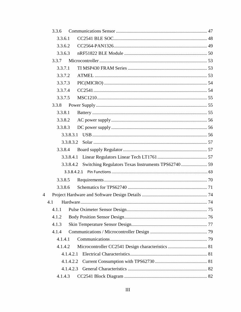
3.2.3 Temperature Sensors
General parameters in this application for temperature sensors are low power
consumption, easy to integrate, and small form factor. Proper power management is
essential for safe operational environment. The sensor will be used to measure skin
temperature on the infant. In Baby Peas project, a thermopile sensor will be used due to
its capability of measuring temperature without skin contact. With high power
14
consumption, the element may be heated and cause discomfort. Fire hazard is another
issue since cloth may be used to conceal the element. With numerous temperature chips
available on the market, our goal is to acquire one that can be easily used with our
microprocessor. Many microprocessors are under consideration but CC2541 from Texas
Instrument meets all the requirements. Sensors that are compatible with CC2541 are the
top candidates in this application. Some models of microprocessors are equipped with
internal temperature; however, they are read the temperature of the chip, and not
necessarily the ambient temperature. A separate chip is needed because the size of the
sensor is a major factor to be considered in this project. Many chips met the requirement
but not all are necessarily appropriate. Technologies involved with the sensor type
include - thermistor, thermocouple, resistance temperature detector (RTD), and
semiconductor. As seen in table 3, technology using semiconductor provides excellent
accuracy and repeatability as well as low heat generation.
Table 3 Thermo Sensor Technology. Reprinted without alteration with permission
by Texas Instruments
The application requires small form factor in order to be applied to the ankle on an infant.
Using semiconductor based sensors, we can achieve ultra-low power consumption with a
form factor less than 3 mm2.
3.2.4 Body Position Sensors
Being able to tell what position the baby is in is a critical design specification of the Baby
Peas’ project. Position of the baby was at the top of a list of 10 steps to help prevent
SIDS from a current WebMD article sponsored by Johnson’s baby [35]. The CDC

15
(Center for disease control) states since the 1990’s, SIDS related deaths have decreased in
the United States by over 50% since the steps to prevent SIDS have been instituted [36].
The Journal of American Academy of Pediatrics suggests babies should be positioned on
their back while they sleep. If the baby is placed on their side or in the prone position
(sleeping on their stomach) then the risk of SIDS is much higher due to rebreathing of
expired gases and also overheating. Stress is also placed on the baby’s cardiovascular
system during prone sleeping which can increase heart rates to abnormal levels [37].
Since the main goal of this project is to help and aid in the prevention of SIDS, being able
to tell whether the baby is in the prone, side, or back position is vital to success. Position
of the baby can be monitored through a couple of different methods. The Baby peas’
project could keep a camera on the baby being monitored. This idea fits into the goal to
achieve non-evasiveness in the project but creates another external peripheral to integrate
into the system. Since the main peripheral to be implemented has other sensors attached
to it a solution need to be found which can be integrated alongside the other vital signs
sensors to keep costs and development time at a minimum. Some technology solutions
include the accelerometer or gyroscope.
3.2.4.1 Accelerometers
Accelerometers measure acceleration (time rate of change of velocity) of an object with
respect to the Earth’s gravitation. While acceleration is not the object of concern for the
Baby peas’ project, one can derive position from acceleration data because the second
derivative of position leads to solving for acceleration. The following equation models
acceleration as a function of position:
a = acceleration
v = velocity
x = distance/position
t = time
d = derivative notation
Since we are measuring acceleration with the accelerometer, we would need to use the
mathematical method of integration to solve for the position. Now how these devices
actual measure the acceleration ranges from device to device. Some devices use the
piezoelectric effect, which means they contain microscopic crystals which are stressed by
the forces of accelerations. These crystals begin to slightly vibrate which will cause a
voltage to be generated. Voltage proportions can be used to determine levels of
accelerations. Another way is for the device to measure changes in capacitance. This is
done by placing two structures close to each other to form a capacitor and if any
movement occurs the structures could move, causing a capacitive change which can be
monitored as well to determine acceleration. For accuracy purposes, accelerometers can
determine 2 dimensional positions or 3 dimensional positions. Since accuracy is critical, a
3 dimensional device which measures the acceleration at 3 axes is better suited to the
project. Another aspect to pay attention to with accelerometers is their “g” level of range.

16
The g level corresponds to reference points. The “g” values also can be referred to as the
measurement of the acceleration component of gravity on Earth, which is 9.8m/s2. So
Earth’s gravity is 1g.[39] While a higher ‘g’ may mean the range is greater it does not
necessarily mean the precision is better. If the object in which we are trying to measure
isn’t going to accelerate at more than +/ 2g’s, then there is no reason to have a device
which can measure up to 24g’s. Determining what the max acceleration a human body
part can move in terms of ‘g’ is important and will be a factor in the choice of an
accelerometer device. Sensitivity of the device can be determined by the change in
output voltage divided by the change in g. The higher the g the more sensitive the device
will be; so the project needs to look for a device which has a high g. Having an
accelerometer device in the Baby peas’ project would be a possible solution for solving
position. Accelerometer semiconductor devices range in price, size and accuracy. The
most important piece when choosing which device and the trade-offs associated with it
will be its power consumption related to accuracy and price. Another aspect is whether
we want a device which outputs a digital signal or analog signal. If we choose an analog
output then the microcontroller we choose will have to have its own built in analog to
digital converter (ADC) circuitry. If analog is chosen, an external ADC may also be used
but this drives up the cost and takes up more space on the circuit board. If a digital
output accelerometer device is used then the importance comes into play on whether it
supports SPI, I2C, or UART. [38]
3.2.4.2 Gyroscopes
Gyroscopes unlike accelerometers measure the angular velocity around a specific axis.
Gyros have the unique ability to be unaffected by gravity whereas accelerometers are.
Gyroscopes are commonly used to give orientation of an object which is still in motion.
Gyroscopes like accelerometers are still references about an X, Y, and Z axis plane
system. Sometimes these axes’ can be referred to as roll, pitch, and yaw. The Gryo
measures the angular velocity in units of degrees per second. The Baby pea’s project can
use this information to determine the position of the infant. Gyroscope devices, like
accelerometers, offer analog and digital outputs. So the design would be similar either
for an accelerometer or gyroscope.
3.2.4.3 IMU
Accelerometers and Gyroscopes both offer unique measuring tools on their own, but
looking for a device which combines both into one would be the ideal situation for the
Baby pea’s project. An IMU is such a solution. The IMU combines both the
accelerometer and gyroscopes functions to provide the designer with 6 axes’ to derive
positional data from. Now these calculations can be determined by using both an
accelerometer IC and Gyroscope IC on the baby pea’s printed circuit board and utilizing
the data from both sensors to determine position or a combined one chip solution can be
realized which gives a digital output over SPI, I2C, or UART to the microcontroller.
3.2.5 Wireless Technology
One of the striving features for the Baby pea’s project was to create something that was
non-evasive. Conventional baby vital sign monitors are almost exclusively wired
technology and only available by going to the doctor. The commercial industry standard
for monitoring anything in the home setting is with video and audio streaming. While

17
these are non-evasive and wireless technologies they do not provide the necessary tools
for gathering heart rate, oxygen levels, and skin temperature but do provide baby
positioning information if a video option is taken. Although a product offering a video
monitor does not provide positional data unless the user is explicitly looking at the video
screen of the monitor. Thus the user could be unaware of the position of the infant
because the display device will not actively warn when the infant has turned to the side or
stomach. So to avoid the clunky and extremely evasive technique used in hospitals and
doctor offices (wired), the project has to use a wireless technology to be able to monitor
the sensors implemented without much intrusion. In doing this some hurdles must
overcome. There are 8 main areas of concern to include battery life, range, data transfer
rates, data security, ease of implementation according to project schedule limits, heat
dissipation, and network topology constraints. Finding a wireless technology which
supports all these features in an advantages way requires consideration of all relevant
wireless technology and a final comparison to see which one fits best for the
specifications and cost requirements.
3.2.5.1 Bluetooth
Bluetooth is another widely used wireless technology. It, like WI-FI, utilizes a
Master/Slave network. Bluetooth can have 1 master and 7 slaves which are formed into a
piconet.[30] It has an IEEE 802.15.1 standard protocol certification but the protocol is no
longer controlled by IEEE 802 but instead is run by the Bluetooth Special Interest Group.
This group is made of over 19,000 members in the consumer electronics industry.[34]
Bluetooth works in the ISM band of 2.4 GHz. It uses frequency hopping spread spectrum
technology which can help in the avoidance of interference of other ISM devices
transmitting in the 2.4GHz spectrum. It uses GSFK (Gaussian Frequency-shift keying)
modulation and supports all Network topologies (Mesh does need special application
enabling). Bluetooth is especially designed for low power consumption. Its range
depends on different protocols and individual setups but can vary between 1 meter to 100
meters. This meets our specification limits for range. Components are very low cost and
the design parameters for Bluetooth are geared towards a quick time to market approach.
This is good for the baby peas since we have a limited time constraint for development.
Bluetooth is also prevalent and almost all cell phones, laptops, and tablets. Bluetooth is
also certified and one of the preferred technologies being pushed by the non-profit
organization Continua Health Alliance which seeks to set industry standards for health
technologies. There are two different protocols to discuss dealing with Bluetooth which
are Bluetooth Classic and Bluetooth LE (Low Energy). [34]
3.2.5.1.1 Bluetooth Classic
Most of the specification for Bluetooth classic is already covered in the above paragraph.
The max range is approximately 100m. Data rates of 1-3Mbits/s. It’s voice capable but
takes around 100ms to transmit data packets. Its peak current consumption is around
30mA
3.2.5.1.2 Bluetooth Low Energy
Bluetooth LE is the newest version of the Bluetooth standard. It can also be called
Bluetooth v4.0 and Bluetooth Smart. It has some stark differences between previous
versions. One of them is Bluetooth LE is not backwards compatible with previous

18
versions of Bluetooth. Bluetooth LE hardware is different from previous versions. It still
uses the same topologies, but Bluetooth LE is geared heavily towards low energy
consumption. It has a reduced range of 50 meters, which still meets our range
specification. While it still uses GFSK modulation the LE version does not transmit on
79 channels but rather on 40 channels which are 2 MHz wide. It has a maximum transmit
power out of 10mW. The data transmit rate is 1Mbit/s but the transmit time is only 6ms
which contributes to less power consumption. Most LE devices operate in single mode
which means they only operate using the Bluetooth LE protocol stacks, but there are
devices which are dual mode which means they can operate either Bluetooth Classic or
Bluetooth LE. These devices are called Bluetooth Smart Ready.[30]
Pros:
Extremely Low Power Consumption
Battery life using a CR2032 can last up to a year in some applications
Data Rates needed meet specifications
Protocol Stacks are already available
Numerous Vendor supported products
Compatible will almost all smartphones, tablets, and laptops
Compatible with all OS platforms
Very secure (128 bit encryption)
Minimum interference from household devices using ISM band due to frequency
hopping technology.
Software implementation is made easy with plenty of vendor support
Cons:
Max range on LE is 50 meters
Sometimes making a connection between two Bluetooth devices can be difficult.
3.2.5.2 WIFI
WI-FI is one of the most widely used wireless technologies available for home use.
Around 61% of households within the United States have a WI-FI network according to a
research study from Strategy Analytics Connected Home Devices services.[32] WI-FI has a standardized protocol through IEEE 802.11. It uses a star or point to point topology
which basically means one WI-FI devices acts as the Master and it can have multiple
slave WI-FI devices it connects too. The slaves can only talk with the master and not the
other slaves. It has very high bit transfer rate (300 Mbps), great security (WEP, WPA,
WPA2), operates in the ISM (Industrial, scientific, and medical) radio band of 2.4 GHz
and 5 GHz, range of 35 meters indoors, high power consumption. WI-FI has potential to
be used in the baby peas project because of its great range and compatibility with mobile
phones, tablet PC’s, laptops, and Smart TV’s, and Gaming consoles which all have WI-FI
integrated circuits which support the 802.11 standards. Some of the concerns with WI-FI
are the high power consumption and ease of implementation.[30]
Pros:
High Data Rates
Less interference if transmitting in the 5GHz range

19
Compatibility with most consumer electronics
Exceeds Range specifications for project
Protocol support plentiful
SOC (system on chip) solution
Cons:
High power consumption
A lot of interference at the 2.4GHz range
Not so easy to implement
3.2.5.3 ZIGBEE
Zigbee is a wireless technology suited for low power consumption applications. It is
maintained under the IEEE 802.15.4 standard. Its main applications are wireless control
and monitoring which is exactly what is needed for the baby pea’s project. Zigbee uses
mesh network topology which basically means there is one Master and many slaves but
the slaves can relay messages from one to another. If one of the Zigbee devices breaks
down it’s still possible to get the data received or transmitted by another Zigbee device
handling the data. Zigbee operates in the ISM band of 868 MHz, 915 MHz, 2.4 GHz.
Transmission data rates are around 250Kbit/s for the 2.4GHz frequency range and max
ranges are around 20m which is a problem for the baby pea’s project. Zigbee operates on
16 channels which are 2Mhz wide and 5Mhz apart.[31]
Pros:
Low power consumption
Cons:
Does not use frequency hopping which could cause interference with most household devices using the 2.4GHz ISM frequency range
Low data rates
Vendors moving away from supporting
Difficult to implement
3.2.5.4 ANT/ANT+
ANT and ANT+ are proprietary wireless protocol sensor networks. Its main applications
are for sport and home health. It also operates in the 2.4 GHz ISM band. ANT products
come preloaded with protocol software packages and are controlled through UART, SPI,
or USB. It has low power consumption and can operate on a coin cell battery. It can
support all network topologies. There are 8 channels and they are bi-directional. It uses
adaptive isochronous network technology to avoid interference with other household
products transmitting in the ISM RF spectrum. Data rate is 20kbps. Range is 30m.[33]
[30]
Pros:
Uses all Network Topologies
Low power consumption
No sensor slave limit

20
Extremely fast transmit time :
Cons:
Not all new smart phones support ANT/ANT+
Lower Range
Low Data Rate
Usually transmits on a single channel for each device. If that particular frequency is not free within the band it halts data transfer and could potentially have packet
lose.
3.2.5.5 Zwave
Z-wave is another proprietary wireless technology aimed at home automation. It operates
in the 900MHz range. Z-wave uses low-latency communications of small data packets.
The data rates are around 100kbps. Its range is around 30m. It uses a mesh network
topology and its modulation mode is GFSK.[31]
Pros:
Low power consumption
Up to 232 devices on one mesh network
Simple protocol and faster time to market
Does not interfere with the crowded ISM band of 2.4GHz
Cons:
Low data rates
Only 1 source for z-wave components and they only sell to OEMs, and ODMs
Range might not meet specifications for project.
From an analysis of all the available wireless technologies the Bluetooth Low Energy
technology seems the best suited for the baby pea’s project. Due to low power
consumption needed and a wealth of vendor support and example projects for both
software and hardware implementation the Bluetooth Low Energy solution fits best.
3.2.6 Data Communications In computer architecture, data is communicated between components using a bus. Buses
are also used to communicate between multiple computers. Buses can be differentiated
by the method of transmission, differentiation of bits, and authority to transmit. The
method of transmission can be either single-ended or differential signaling. Single-ended
signaling is the transmission of an electrical signal through a single wire. The transmitted
voltage is compared against a ground voltage to determine if the bit is high or low.
Differential signaling sends two signals across two paired wires, called a differential pair.
The difference between the two signals is analyzed to determine if the bit is high or low.
The advantage of differential signaling is the ability to deal with electronic noise. When
an electric signal is affected by noise in a single-ended transmission, the received signal
can be misinterpreted due to the change in voltage. In a differential pair, noise will affect
both wire the same. Theoretically, the difference between the wires should stay about the
same so the information sent would be unaffected.

21
A bus can also send the data through serial communication or parallel communication.
Serial communication sends data one bit at a time across the bus. Parallel
communication sends several bits at a time on parallel channels that are assembled to
retrieve the original message. Due to cost and complexity, most buses are serially
communicated. Devices may support bus mastering, which enables the device to initiate
the transfer of data across the bus. Depending on the nature of the hardware and
software, multiple master nodes may be necessary for certain devices.
3.2.6.1 I2C
I2C is a multi-master serial single-ended computer bus invented by Philips.
3.2.6.2 SPI
The Serial Peripheral Interface bus (SPI) is a synchronous serial data link developed by
Motorola that operates in full duplex mode. Full duplex implies that the link can send
data both ways. A data link is synchronous when data is transferred on a clock cycle.
3.2.6.3 UART
A Universal Asynchronous Receiver/Transmitter is a piece of computer hardware that
translates data between parallel and serial forms. This type of data transfer is considered
“universal” because the data format and transmission speeds can be configured.
3.2.7 Mobile Applications
The project is going to be using a mobile application as the user interface. A mobile
application is a piece of software designed to do a useful function beyond the basic
functions of making the computer run. Multiple mobile services offer the ability to
download and run applications on their mobile operating systems. This includes the
Apple App Store, Google Play, Windows Phone Store, and BlackBerry App World.
3.2.7.1 IOS
The iOS is the operating system used for the products developed by Apple Inc., such as
the iPhone, iPad, and iPod Touch. The iOS is based off the OS X kernel. Software
applications for the iPhone or related products can be downloaded on the Apple App
Store. The Integrated Development Environment for Apple products is called Xcode.
Xcode supports source code in C, C++, Objective-C, Objective-C++, Java, Applescript,
Python, and Ruby programming languages. Xcode is one of the features on the iOS
Software Development Kit, which also include the iOS Simulator, iOS Platform-tools,
and Interface Builder. The iOS user interface is programmed through a framework called
Cocoa Touch. This controls the actions of the touch-screen interface and its interactions
with the operating system. Applications for the iOS are usually programmed in a C
language (C, C++, C#).
3.2.7.2 Windows Phone
Windows is the operating system developed by Microsoft and is used in most Microsoft
products, including many desktop computers, smart phones, and the Xbox. The latest
version of Windows is Windows 8. Many programming languages are supported by
Windows Store apps. These include Java, HTML5, C#, Microsoft Visual basic, XAML
(Extensible Application Markup Language, Visual C++ component extensions, C++, and

22
Microsoft DirectX. The development environment used for Windows is the Microsoft
Visual Studio Express 2013. It includes the Windows Software Development Kit, Blend
for Visual Studio, and a device simulator to test out the Windows Store apps that are
created. There are available templates for beginners to understand the basic structure of
an app. Windows has also developed a cloud computing platform called Azure, which
provides both platforms as a service (PaS and Infrastructure as a service (IaaS).
3.2.7.3 Android
Android is an operating system based on the Linux kernel. Android is owned and
developed by Google. After an update is released, the operating system is open-sourced
and allows the Android community and consumers to alter and add on to the operating
system, where new features and improvements can be implemented if deemed
appropriate. Bugs in the operating system and efficient programming can be more
quickly dealt with in this way. Android applications can be downloaded through the
Google Play store or the Amazon Appstore. To begin developing an application as a
third party, the Android Software Development Kit must be obtained. This can be
achieved by purchasing the ADT Bundle from Android. The bundle includes the Eclipse
Integrated Development Environment plugin, ADT plugin, Android Platform-tools, the
latest Android platform, and the latest Android system image for the emulator. Android
apps are usually programmed in Java. [56]
3.2.8 Microcontroller / FPGA
The microcontroller is an essential part of the overall project. The function and data flow
of the sensors is determined by the microcontroller. When selecting the appropriate part
for the wireless sensor, the performance and power consumption are the primary
specifications to consider. This is because the microcontroller will be mounted on a
peripheral unit and act as part of a wireless transmitter. The MCU should use a minimal
amount of power to maximize battery life while being able to achieve the necessary
performance standard needed for its actions. The data processing required will have to
do mostly with interpreting analog data coming off of multiple sensors measuring vital
signs and position. The microcontroller needs to have at least 4 analog to digital
converters, one for each sensor, and a minimum sampling rate of 8 bits of resolution.
The microcontroller will also interface with a Bluetooth wireless system and thus must
have both SPI and I2C in order to have the flexibility to integrate sensors into the system.
3.2.9 Power
The power supplied for this project come from two sources, alternating current from the
main electrical grid and direct current from battery or power supplies such as those in a
PC connected through a USB. In addition to the two types of power source, the unit also
uses linear or switching regulator integrated chips to help provide steady power to the
modules on the satellite unit.
3.2.9.1 Power Considerations and Safety
There are a number of considerations to be made for the power subsystem. As integrated
components shrink and get more efficient, one of the most important decisions that
decide the final product and packaging is power. In order to provide the needed
functional length and reliability, the power subsystem tends to take up the majority of
space and weight in the product.[x] For this project in particular, the sock unit needs to

23
be lightweight. It would be onerous, and maybe even dangerous, for a baby to be
wearing anything to heavy. In addition, since this unit is being used to monitor health
effects, the power source chosen cannot have weak points in its delivery system or
longevity. Providing a seamless experience for the user requires attention to safety
measures, efficient usage of power, longevity of operating hours, easy and fast recharge
time, and noninterference with the other modules on the unit.
3.2.9.1.1 Safety
Safety is first and foremost due to the sensitive nature of the environmental conditions
during operation. The satellite unit not only functions in close proximity to humans, it is
primarily designed for users with limited verbal communication, making it hard for the
caretaker to gauge feedback on operation and physical status of the unit in the event of a
malfunction. In the worst case scenario a runaway heating issue could cause burns on the
baby or a shock hazard could happen and cause irreparable damage. The unit has to have
safety measures in all aspects, taking in considerations such as shorts and unduly
dissipation. Admittedly, there is little chance for arc flash or arc blasts due to the voltage
being less than 240, according to the National Fire Protection Association. [42] The baby
pea unit itself limits the voltage to a much lower 3.7 volts. However, since the unit is
worn against the skin, electric shock and thermal damage does exist. In addition, it is not
the voltage that is the primary concern, but the delivered amperage that can harm or kill a
person. According to an Ohio State University resource, a shock as low as 10 milliamps
can cause a painful shock to an adult. Lethal currents occur starting at 100 mA. Some of
the symptoms of electric shock include muscle paralysis, difficulty in breathing, severe
burns, ventricular fibrillation, cardiac arrest and death.[42] As table 4 lists, a current as
low as 5 mA can cause a painful shock to an average adult individual. At around 6-16
milliamps, the victim will start to lose control of their muscles, and this is known as the
let go range due to the fact that any higher amperage can cause spastic contraction of the
muscle fibers and prevent the victim from letting go of the live wire. The range of effects
is listed in Table 4.
Current Level in
Milliamperes
Probable effect on Human Body
1 Perception level. Slight tingling sensation. Still dangerous under
certain conditions.
5 Slight shock felt; no painful but disturbing. Average individual can
let go. However, strong involuntary reactions to shocks in this range
may lead to injuries.
6-16 Painful shock, begin to lose muscular control. Commonly referred to
as the freezing current or let go range.
17-99 Extreme pain, respiratory arrest, severe muscular contractions.
Individual cannot let go and death is possible.
100-2000 Ventricular fibrillation and muscular contraction and nerve damage
beings to occur. Death is likely.
>2000 Cardiac arrest and internal organ are damaged. In addition, victim
will have severe burns. Death is probable.
Table 4 Effects on human body due to different amounts of current [43]

24
Although fat tissue is a bad conducting material, and the baby might be protected
somewhat due to high fatty tissue, the overall threshold for damaging current level is
undoubtedly lowered for a baby due to a much lower body mass. A shock that will not
cause lasting effects in an average adult can irreparably harm a child. According table 4,
a current as low as 100 milliamps can cause ventricular fibrillation in healthy adults.
That is enough to kill the said adult. In a child, with a mass order of magnitude smaller
than a healthy adult, the100 milliamps potentially becomes lethal by the same order of
magnitude. In addition, even if the shock does not cause visible signs, the perception
level will cause discomfort to the baby. For a portable circuit, there is no way to bond the
circuit to an effective ground-fault path. If the unit inadvertently gets knocked around
and expose circuitry, the baby might very well exposed to a lethal current, and the
caretaker will have no knowledge of this other than the fact that the baby might cry more
or display signs of discomfort that might be attributed to other factors such as hunger or
the need for a diaper change. In addition to shocks, burns are another concern when
dealing with power supply. If there is not enough adequate heat dissipation the circuit
can overload thermally and burn the wearer. The degree of burn is usually a factor of
both the thermal level of the object and how long the object is in contact with the skin.
Often times, this kind of burn is insidious in nature due to the fact the person being
burned does not realized that. The thermal level of the object could be tolerable to the
skin, but when taken into account duration, can become deleterious. Just like the
harmless feeling of sunbathing, thermal burns sneak up on the user and can have
devastating consequences. In fact, there have been cases of serious burns caused by
overheating battery packs of laptops. Those incidences involved adults that received the
burns unknowingly over a period of hours as they used the devices on their laps and in
contact with their legs. Table 5 shows the gradual gradation between the comfortable
temperatures to temperatures that can cause irreparable damage.
Body Temperature
(degrees
Fahrenheit)
Signs and symptoms
100-110 Brain Damage, fainting, nauseous feeling
98.6 Normal body temperature
90-98.6 Shivering and goosebumps
80-90 Lose power of speech
70-80 Potentially irreversible cooling
60-70 Lowest temperature with recovery
<70 Irreversible recovery
Table 5 Physiological reactions to body temperature. [47]

25
A baby would be much more susceptible to thermal agitation on its skin. Along with
slow heating, the different types of batteries have levels of volatility. The battery type
chosen must have long stable life with little to no risks in explosions. In addition, to
when the unit is used against the user’s skin, the charging portion deals with addition
risks as it is going to be connected to a wall socket with the potential of 120 volts. The
charging station will need an adequate charging unit with transformer to step down the
voltage to the acceptable amount for the circuit. With adequate circuit protection,
component selection and circuit board design, these challenges should pose no issue in
the final product.
3.2.9.1.2 Operation
After safety, the second design consideration deals with operation. To fully realize the
potential of this unit, a priority lies in length of operation and recharge ability of the unit.
Designed to last 8 hours a day, Baby Peas will give the caretaker sense of security in its
quality performance without the interruption of charging and exchanging out units. Each
sock unit should last a day’s worth of monitoring. In addition to the battery life of a day,
each unit should also be recharged within a reasonable amount of time. This is to ensure
quick overturn term if needed and give flexibility to the user, whether at home or on
vacation. In addition, each time the sock is exchanged out would mean device wearing,
which can prematurely lower life time usage. This is in addition to the issue of weight
and scale. All of these need to be considered when searching for the portable DC supply.
Some viable options include AA batteries, button batteries, or super capacitors.
Super capacitors are a very attractive option. They have rapid recharge time, have less
wear with constant recharging and discharging, and function well under different
temperature variations8. They are also extremely stable as they use stored static charge
rather than energy from chemical reactions. Lithium ion, when exposed to air, is very
volatile and can be explosive. The unfortunate thing about super capacitors is size at this
time. With current state of technology, a super capacitor is power dense (able to
discharge and consequently recharge rapidly), but it is not energy dense (for the
comparable size of a batter package, it holds much less charge). In order to have
sufficient power for the unit, size would have to be sacrificed. For traditional chemical
batteries, the button battery would be the best package for the baby peas unit. It is the
lightest in terms of weight, one of the longest continuous usage options, and is often used
in medical applications. While danger does exist in the chemical nature of the battery,
the packaging is safe enough for usage that these batteries are often used in the hospital
setting or with every day consumer goods.[44]
3.2.9.1.3 Interference Considerations
In addition to being a reliable power source for the electronics and peace of mind, the
power subsystem also needs to consider causing interference with other subsystems. In
general, the different components of a circuit are taught as idealized versions, with no
interference among the different components. However in practice, parasitic inductance
and capacitance are serious issues that can impact usage hours and quality of usage.
According to source [x], “any two conductors will have a capacitance between them, any
conductor used for carrying current will have inductance, and parasitic capacitance and

26
inductance create reactive impedance that varies with frequency”. For the first point, the
capacitance formed between two conductors is given by the equation:
C = capacitance
q = charge
V = voltage
Inadvertently, capacitance can be formed from “parallel trace runs, or by traces over a
ground or power plane”.[46] In addition, the wires running the power throughout the
circuit also create capacitance.
The general inductance formula is given by [46]:
µ = the magnetic permeability of the material
A = the cross-sectional area of coil
l = the length of the solenoid
In addition the normal use intended induction, parasitic inductance effect is given by
[45]:
Z=total impedance
w=omega
C=capacitor value
Lparasitic=parasitic inductance
Utmost care must be taken in the satellite unit to rid of any preventable noise. As the
module is quite small and low powered, any noise can have a catastrophic effect on
proper operation.

27
3.2.9.1.4 Electrostatic Discharge Protection
Finally, a mention of electrostatic discharge is in order to the sensitive nature of the
components. Working with open boards is a recipe for disaster without proper ESD
protection schemes. Table 6 shows the minimum volts that can start to damage the
devices.
Device type ESD susceptibility threshold(V)
MOSFET 100
JFET 140
CMOS 250
Diodes 300
Transistors 300
SCR 600
Table 6 ESD thresholds for common devices [48]
The values might seem high, but the simple act of walking across a carpet can generate
up to 35,000 Volts.[38] Table 7 shows some additional voltages that can happen.
Static generation Electrostatic voltage (V) at 10% relative
humidity
Walking across vinyl floor 12,000
Worker at bench without wrist strap 6,000
Styrofoam packing 120,000
Picking up common plastic bag 60,000
Table 7 ESD generation from various activities [48]
ESD prevention is a mixture of technique, workstations and atmosphere. At the crux of
electrostatic protection is keeping the potential between the technician and the board the
same. Because the work on this project is being done during the winter, it is crucial to
make sure that the surrounding atmosphere of the work area is high in humidity; the
lower the humidity, the easier for static to build. A humidifier could help with this, or
even leaving out a body of water can help. In addition, all of the workstations where
component touching can happen, whether it is soldering or just simple handling, need to
be grounded to a common ground. A simple dissipative mat, wrist strap, and finger cots
can help prevent potential different buildup on the person’s body relative to the board.
Each of those components help drain the body voltage and prevent body voltage buildup.
In addition, they are often nonintrusive and cheap. Finally any transportation of the

28
boards or sensors outside of the final packaging must be carried with shield bags. Note,
ESD protection is for non-energized work. Remember to take adequate precautions when
working with live circuits, as discussed in part 3.2.9.1.1
3.2.9.2 AC Power
The AC power component is primarily used for recharging the power supply for the unit.
In the alternating current source, in order to be able to use the potential, components like
transformers, rectifiers, filters, and regulators needs to be incorporated. After the
Transformers help to step down the 120/240 AC down to usable voltage for the power
supply, rectifiers in formations such as a full wave rectifier help to covert the sinusoidal
supply to a rectified waveform. This, rectified waveform is smoothed out by the filtering
capacitor.
Figure 5 Simple rectifying circuit
An example circuit, Figure 5, shows how an incoming sinusoidal wave is stepped down
at the transformer, and then rectified at the bridge rectifier made of four diodes, and
finally smoothed out by capacitor, C1. The output of this circuit is a direct current at a
usable voltage. In the baby peas unit, this DC voltage is used to charge the rechargeable
battery. Figure 5 is an over simplified unit and lack any sort of circuit protection. Fuses
will need to be incorporated to protect the circuitry. While it is theoretically possible to
build an AC power supply unit for this project, it is recommended to forgo this subsystem
due to extreme hazards of working with live mains power. Without Occupational Safety
and Health Administration’s (OSHA) rated personal protection equipment such as
goggles, hard hats, gloves, face shields, and clothing, which all cost a considerable
amount, it is foolhardy to build an AC power supply. It is recommended to buy an off the
shelf AC power unit for this project.
3.2.9.3 DC Power
DC to DC power supply is used in two aspects—recharging the unit via solar power and
supplying power to the different modules in the unit.
3.2.9.3.1 Solar Power
A generic solar power unit consists of the Photovoltaic cells, the combiner, inverter and
storage unit. The inverter is used to turn the solar generated DC power into AC as most
of the solar units are used to supplement mains power. If the baby peas unit is charged
via solar power, this inverter step is not needed. Photovoltaic cells basically work under
the principle of the photoelectric effect of some materials. As photons strike the surface,

29
energy is collected and transformed into a current. Figure 6 shows a simple set up of the
process.
Figure 6 A basic photovoltaic cell operation diagram created by Xin Tong in
MSword
Using a number of cells in modules and set in arrays, a multitude of these cells can
harvest a considerable amount of power from the Sun. Amorphous photovoltaic cells
would be the cheapest options, but is the least efficient and have the least lifespan. Both
Monocrystalline and polycrystalline are good choices. If the project basic goals are met
and the decision is made to focus on a stretch goal, either monocyrstalline or
polycrystalline would be a good choice. It is recommended that the decision be made on
the side finance and polycrystalline be the choice due to its lowered costs and comparable
characteristics with the monosyrstalline offering. In addition there is a breaking in period
for the cells. There are many available schematics for simple solar cell phone charger.
The voltage for a phone is around the voltage needed for the module so a solar charger is
a very viable option. Several issues to consider in designing the solar unit:
Solar panel collapse: Figure 7 shows the solar cell I-V curve in varying sunlight. At each
level, there is an optimal power point. Following the red line, at a certain point any slight
increase in current will cause the voltage to drop to 0. The maximum amperage is 0.034
A. At the second line, a lighting condition less optimal than the first line, the maximum
amperage is 0.026 A. So imagine if a solar charger is operating at full sunlight and
supplying the maximum amperage of 0.034 through the circuit, any changes in lighting
condition without changes in the current draw would immediately drop the voltage down
to 0. [57]

30
Figure 7 Provided by the openware documentation from Adafruit industries, shows
an current-voltage curve of solar cell performance under varying sunlight.
A charging unit has to sense the available current from the solar cells. If the circuitry
tries to pull the same amount of current under changing conditions, then the voltage can
collapse and the charging action is stopped. This undermines efficiency. Reverse
leakage protection: This actually is an issue when there is a storage element in the
circuitry. The stored element can leak charge back to the source if the stored element, in
the case, the battery, has a higher potential, than the source.
Figure 8 Schematic for phone charger. Created by Xin Tong using Cadsoft Eagle

31
Figure 8 gives the circuit of a general solar to USB phone charger.[54] The solar cell
used here is the 750-00032 manufactured by Parallax and costs $59.99 per unit. The
specifications for this cell are 10W power, 18V at Pmpp, and 580 mA at Pmpp. While
this unit is very powerful, a better price point could be found with less powerful solar cell
that would use a switching regulator. The switching regulator is a good recommendation
for the charger due to high efficiency. Noise is not a consideration because the satellite
unit would not be transmitting or receiving information when it is docked in the charging
station. In addition to the basic phone schematic, an energy storage unit needs to be
added, for flexibility in usage and for lower component cost. Due to the two issues
discussed above, voltage collapse and reverse leakage, a chip such as TI’s BQ24210 unit
would be ideal in implementing in a charging circuit. While is nice to have this module
to supplement the main AC source, it might prove too ambitious for a single semester
project to build this additional module. If time is sufficient, this building this module
would very instructional to solar power circuitry and pitfalls.
3.3 Strategic Components
3.3.1 Pulse Oximeter Sensor AFE4490
Choosing a sensor that is compact and high integrate capability along with low power
consumption is top priority. Under close evaluation, Texas Instruments AFE4490 is the
most suitable for this project. It is compatible to multiple microprocessors and wireless
Bluetooth modules with maximum 5.25V required. Its QFN-40 (6mm x 6mm) form
factor is ideal for implementing with other sensors in small projects. AFE4490 uses SPI
(Serial Peripheral Interface) as the communication bus to send digital data to the MCU. It
has configurable LED circuit drive current which low voltage can be achieved. The
receiver front end includes photodiode, current to voltage converter done by TIA
(transimpedence amplifier.) Ambient cancellation scheme estimates amount of ambient
light leakage by sampling ambient light with two LED sending data to SPI and
transmitted to the MCU. The MCU has the information of all the data and able to
estimate the amount to be subtracted. External 8 MHz crystal generates the frequency
responsible for controlling the clock cycles. 4 MHz is used for timer modules, ADC, and
the diagnostic.
The detailed pin configuration can be seen in figure 9. To integrate AFE4490 with the
microprocessor, a basic understanding of pin function is necessary. The pins can be put
into five categories based on functionality. Each category is summarized in table 8. Note
the tables do not contain all the pins but the pins which are used or discussed.

32
Figure 9 Pin Configuration of AFE4490. Reprinted without alteration with
permission from Texas Instruments
3.3.1.1 Analog Pins
Pin 1 and 2 are analog pins connecting the photodiodes with wavelength 660nm and
940nm with analog ground common ground pin 3, 36, and 40. Block diagram and pin
connection will be discussed in hardware section 4.1.1
Name No. Description
INN 1 Receiver input connected to photodiode anode
INP 2 Receiver input connected to photodiode cathode
RXOUTN 34 External ADC negative input on bypass mode
RXOUTP 35 External ADC positive input on bypass mode
TXN 14 LED driver out B, H-bridge output connected to LED
TXP 15 LED driver out B, H-bridge output connected to LED
Table 8 Analog Pins and Description
3.3.1.2 Digital Pins
Some of the digital pins are made for fault detection or reset. Two of them are for
connection to an external 8-MHz crystal. For complete details, please refer to AFE4490
user guide available on Texas Instruments website.

33
3.3.1.3 Supply Pins
The supply pins are mostly connected to the external power supply or to the common
board ground. Decoupling capacitors are required for certain pins. They are not discussed
in details.
3.3.1.4 Communication Pins
Name No. Description
SCLK 24 SPI clock pin
SPISIMO 25 SPI serial in master out
SPISOMI 26 SPI serial out master in
SPISTE 27 SPI serial interface enable
Table 9 Communication Pins and Description
The communication pins provide data transmission from AFE4490 to CC2541 via SPI
protocol. Please refer to hardware section 4.1.1 for details and block diagrams.
3.3.1.5 Reference Pins
The reference pins are connected to decoupling capacitors and the ground. Pin 5, 6, and
10 are open circuit pins and should not be connected to anything.
In conclusion, AFE4490 provides complete solution to analog front end pulse oximeter
sensor. Not only it provides many fault detection, but also many advanced features such
as ambient light correction and precise timing controller. SPI interface will work well
with CC2541 for data transmission. It could take extra time to configure the
communication bus since the other sensors use I2C protocol. Interrupt function will be
written for incorporating the sensors communication. AFE4490 is the most qualifying
analog front end for Baby Peas Project.
The detailed package dimensions are seen in Figure 10. The measurements are important
for PCB layout. Cadsoft Eagle is used for creating AFE4490 and the package dimension
was taken into consideration.

34
Figure 10 Package Dimension of Texas Instruments AFE4490. All the
measurements are in mm. Reprinted without alteration with permission by Texas
Instruments.
3.3.2 Alternative Design of Analog Front End Pulse Oximeter
AFE4490 offers many features but not all necessary. A Simplified analog front end can
be designed with basic components and may reduce power consumption. A design of an
analog front end can be broken down into a few key components. System diagram are
shown in Figure 11.

35
Figure 11 System Block Diagram for Analog Front End Design
A digital to analog converter sends signal from microprocessor. When it reaches
amplifier, the signals are boosted up in order for the driver unit to read the timing
sequence for LED. The LED with 660 nm and 940 nm should alternate each other
between on and off. When the photodiode sensor gets excited by the light goes through
the object, two currents are created based on different wavelength of light input. The
signals coming from photodiode sensor are relatively weak and unusable for typical
analog to digital converter. Some noise may need to be filtered out for accurate reading.
The amplifier portion can break down into three parts- pre-amplifier, low pass filter, and
final stage of amplification. Use the pre-amplifier to boost up the currents from the
photodiode sensor. Filter can be a simple low pass filter or Butterworth filter for
enhanced quality. A final stage of amplifier boosts the currents to match the operational
spectrum of analog to digital converter. The currents are converted into voltage and
transmitted to corresponding pin on the CC2541 microprocessor. Many ADC chips are
equipped with I2C interface which will be easier to use along side with the temperature
and body position sensor.
Digital to Analog Converter
Amplifier
LED Driver for Photodiode
Emitters
Instrumentation Amplifier
Analog to Digital Converter
Microprocessor
Amplifier

36
Compare AFE4490 to a self designed analog front end, AFE4490 offers many additional
features such as current fault detection. While AFE4490 may increase interface difficulty
because of the SPI interface, it does not require any additional hardware. With AFE4490
single chip solution, it may benefit Baby Peas monitor for increased accuracy and
reduced hardware modulation. The price of a single AFE4490 is lower than using
multiple chips with different functions.
3.3.3 Photo Diodes/Photo Diode Sensor
Analog front end incorporated with LED driver is paired with photo diodes. The light
wave goes through blood cells and received by photodiode sensor. As discussed in
section 3.2.2, specific wavelength must be used in order to obtain accurate measurement.
Low power consumption, easy integration, small form factor are the key requirement for
Baby Peas monitor.
Advance Photonix Inc DPI-E839 is a four drive emitter with three emitter diodes with
wavelength 660nm, 880nm, and 940nm. It has very small form factor of 6.73 mm x 6.73
mm x 1.90 mm. It has maximum power consumption of 250 mW and peak forward
current of 200 mA. With a metalized ceramic package, it can be soldered onto PCB along
with other components fairly easy. DPI-E839 is ideal to be used with AFE4490 for Baby
Peas monitor. The only downside is the unit price. It carries a hefty unit price of $5.95
available on Octopart.
QEB363 is an infrared emitting diode manufactured by Fairchild. It can be paired with
QSB34CGR photodiode sensor. It emits wavelength of 940 nm. With a small T-3/4 (2
mm) package and extended lead; it can be mounted in three different configurations. The
overall size without counting the lead is 2.2 mm x 2.5 mm x 3.0 mm. it has a power
dissipation of 100 mW and continuous forward current of 50 mA. Additional 640 nm
LED must be paired with QEB363 for using as pulse oximeter. Marktech optoelectronics
manufactures wide selections of 640 nm light emitters. The particular model best suits
Baby Peas monitor is MTE5066C- UR. It has a similar form factor of 3.1 mm x 3.1 mm x
4.3 mm. Although slighter bigger, the difference can be neglected because their small
size in nature. The power dissipation is 110 mW with forward current of 50 mA
according to datasheet. Combining QEB636 with MTE5066C-UR should have similar
performance of a single DPI-E839.
3.3.4 Body Position Sensor
From an overview of relevant technologies consisting of accelerometers, gyroscopes, and
IMU’s it looks like choosing a component with IMU functionality will be the best choice
for the ability to tell in which position the infant is in during the sleep cycle for the baby
peas project. IMU’s can be extremely costly. Through research it was found that
accelerometer IC’s were more available and low cost with only a few IMU devices in the
price range compatible for this project. A comparison of the IMU’s and Accelerometers
for this project will be considered. Key factors which weigh on the decision will be
accuracy, cost, size, reliability, ease of configuration, ease of solder ability, and of course
power consumption. Since the baby peas vital signs monitor is going to be wireless and
battery powered the two most important factors will be power consumption and accuracy.
With a wide variety of sensor to choose from, a lot of IMU’s and accelerometers offer a

37
special function feature which allows the IC to be put into a sleep mode to conserve
power. Components which offer this feature will be given special consideration.
3.3.4.1 Invensense MPU-60x0 series
The MPU-6000 and 6050 are IMU’s which are integrated onto one chip providing 3-axis
accelerometer measurements along with 3 axis gyroscope measurements. The chip is
also scalable in it provides a dedicated I2C bus to accept an external 3-axis magnometer
which would give 9 axis data measurements. Range of the accelerometer portion consists
of +/- 2g, +/- 4g, +/- 8g, +/- 16g, which are user programmable which means if only +/-
4g range is needed it can be selected and reduce the amount of current the IC would
draw. They gyroscope range is selectable as well consisting of +/-250 degrees per second
(dps), +/- 500, +/- 1000, +/- 2000 dps. The chip also consists of 6 16bit analog to digital
converters (ADCs) to sample all axis points of both the accelerometer and gyroscope. It
boasts an onboard 1024 byte FIFO which allows for the microcontroller interfaced with it
to read data output from the MPU-60x0 series in bursts. This allows the microcontroller
to go into a sleep mode while the MPU collects more samples. The output of the MPU is
digital and compatible with both SPI and I2C (MPU-6050 only uses I
2C). I
2C data rates
are up to 400kHz and SPI data rates are up to 1MHz. The input voltage to the chip is
between 2.375v -3.46v which is in the boundaries of usable input voltage for this project.
Price is around 10 dollars if purchased through Digikey with a lead time of around 2-3
weeks. The MPU also has an additional temperature sensor on the device but this most
likely will not be used since another sensor being used in this project will take care of
skin temperature.
The MPU also has a unique proprietary Digital Motion ProcessorTM
. The DMP offloads
the motion processing computations from the system microcontroller and performs them
on its own chip. This minimizes the amount of processing power consumed by the
system processor. There are different current consumption applications because each
feature of the MPU can be configurable to be either off or on. Since the baby peas
peripheral device wants the desired accuracy it will run all three characteristics
(accelerometer, gyroscope, and DMP) during operation. Running all three options will
result in 3.9mA operating current. This should be well in the desired operating current to
allow for the baby peas peripheral sensor to run through the night. The idle mode
operating current is 5uA with a 100ms ramp rate for the device to return to full operation.
Figure 12 below is a diagram of a standard QFN 24 pin 4x4mm PCB layout example.

38
Figure 12 PCB Layout Diagram for a QFN 24 pin 4x4mm package.
The MPU-60x0 series is a QFN package (Quad Flat Pack no leads). From the Figure 12
above we see there is a substantial ground plane and 24 pins to be soldered. Solder
ability of a QFN can be difficult especially when the total dimensions of the part are
4x4mm (shown by dimension A x B in Figure 12) and each lead is .25mm (shown by
dimension ‘a’). While QFN’s may be considerably harder to solder down it is possible
by using a reflow machine or hot air pencil. The great part about this device is the leads
can be seen from the outside of the component and solder can wick up the sides of the
leads thus letting the user know a proper solder connection has been made. The baby
peas project group has an experienced J-STD-001 certified specialist in soldering of
surface mount components so QFN packages should not be a problem.
3.3.4.2 Analog Device ADXL362
The ADXL362 accelerometer made by Analog Devices is an ultralow power digital
output MEMS system on chip. During a 400Hz data rate output the device is only
drawing 3.0uA with a supply voltage of 2.0v. This is extremely beneficial for the baby
peas project due to the desired lower power consumption on the peripheral device. It has
12 bit ADC output resolution and communicates using a SPI interface to the
microcontroller. Another feature is the device can be programmable to only output 8 bit
resolution if lower resolution is possible. This may prove to be handy if the project
notices accurate readings can be taken utilizing less bit resolution giving it less power
consumption and easier byte transfers. It is a 3 axis accelerometer and has selectable
range measurements of +/- 2g, +/- 4g, +/- 8g with a resolution of 1mg/LSB on the +/-2g
range. Like the MPU-60x0 series the ADXL362 has an onboard FIFO which enables
burst data transfers which allows the system processor to go into a sleep mode while the
ADXL362 is sampling the signal. The device also has a neat feature which allows the
chip to go into a sleep mode when no motion is detected and has an adjustable threshold
for when the chip should be woken up. This way if the infant is motionless there is no
need to run the accelerometer during motionless states. The User Interface can recall the
B
a
Ground Plane
A

39
previous data until the baby moves again and causes the chip to “wake-up” and begin
another sample to re-adjust the position and update the user if the baby has turned to a
harmful state position. This could boost battery life.
Figure 13 Possible PCB Layout for the ADXL362.
Figure 13 of the possible PCB layout for the ADXL362 are the outer dimensions and
recommended PCB layout design from Analog devices. The package is small at 3.5 x
3.5mm (denoted by A X B) 16 pin LGA package with recommended trace widths of
.3mm (denoted by a). The device could prove to be difficult to solder because of its LGA
(Land Grid Array package). Soldering down the component with a soldering iron is not
possible so it would have to be down with a solder reflow machine or hot air pencil.
Another negative to the LGA package is there is no way to tell if the part is soldered
down correctly. This could prove difficult during debugging of the system and rework if
the part needs to be replaced. The part costs roughly 10 dollars from Digikey and is
stocked and ready for delivery.
3.3.4.3 Freescale Semiconductor MMA8451Q
The MMA8451Q accelerometer is low power and boasts 3 axis measurements. It
contains 14 bit and 8 bit resolution onboard ADC’s and user selectable ranges of +/- 2g,
+/- 4g, +/- 8g. It too like the ADXL362 can be put into a sleep mode during motionless
states of the infant being monitored. The MMA8451Q has output data rates of 800Hz.
Output data is transmitted over I2C to the microcontroller. It also has a 32 sample FIFO
which acts similar to the other two devices in question. The supply voltage is from 1.95v
to 3.6v which is in the project operational input voltage. At data rates of 800Hz the
device is drawing 165uA and a mere 1.8uA during standby. Figure 14 below shows the
dimensions of the device.
a
A
B

40
Figure 14 Bottom dimensions of pads for the MMA8541Q. Reprinted without
alteration with permission by Freescale Semiconductors
It’s a 3x3mm QFN. The leads are .3mm in width and .567mm in length. This QFN is a
little different than the MPU-60x0 series in that the leads are not visible from the side
edges of the device. It’s more similar to the ADXL362 LGA package. This again
surfaces the problem of being able to see if the device is properly soldered down. A hot
air pencil or solder reflow machine would have to be used in the mounting of this
component. One of the best features of this device is cost. Digikey shows this device at
as little as $1.82 and the lead time is 0 weeks as this device is stocked and ready for
immediate shipment.
Table 10 below is a breakdown of the three devices along with their respective
parameters side by side for comparison.
Table 10 Comparison table of explored devices for body position sensor
MPU-60x0 Series ADXL362 MM8451Q
Input Voltage (volts) 2.375-3.46 1.6 - 3.5 1.95 - 3.6
Gyro / Accelerometer Both Accelerometer Accelerometer
Range +/- 2g, 4g, 8g, 16g +/- 2g, 4g, 8g +/- 2g, 4g, 8g
Degrees Per Second +- 250, 500 , 1000, 2000 n/a n/a
Operating Current 3.9mA 3uA 165uA
Standby Current 5uA .01uA 1.8uA
Data Outputs SPI and I2C SPI I
2C
Data Output Rates I2C (400KHz), SPI (1MHz) 400 Hz 800Hz
ADC Resolution 16 bit 12 or 8 bit 14 bit
FIFO 1024 Byte 512 Byte 32 byte
Packag Type QFN (leads visible up sides) LGA QFN (leads not visible)
Cost $10.72 $9.22 $1.82
Lead Time 2-3 weeks (Digikey) Ready to ship (Digikey) Ready to ship (Digikey)

41
From table 10 above it looks like the MPU-60x0 is the best bang for the buck. It fits all
categories except for power consumption. The 3.9mA operating current still shouldn’t
affect the battery life of the entire sensor enough to cause concern. Some of the deciding
factors were the QFN package looks to be the easiest to solder down making installation
of the device a bit easier and troubleshooting a little less of a worry. The accuracy is
much higher and this boosts the reliability of being able to provide the most accurate
measurements of position for the consumer. Careful scheduling must be adhered to since
the device has a 2-3 weeks lead time.
3.3.5 Skin Temperature Sensor
The application requires small form factor in order to be applied to the ankle on an infant.
Using semiconductor based sensor, we can achieve ultra-low power consumption with a
form factor less than 3 millimeter squire.
3.3.5.1 TMP006
The first candidate under consideration is TMP006 from Taxes Instruments. TMP006 is
meant for non-contact remote temperature monitoring. TMP006 is an infrared thermopile
sensor with a size of 1.6mm by 1.6mm. The temperature of the object is measured by the
thermopile on the sensor. The thermopile converts thermo energy (infrared energy
emitted by the object in this case) into electrical energy. An output voltage is created
based on the difference to the local temperature. TMP006 operates between minus 40
degree Celsius to 125 degree Celsius. The way TMP006 communicates is thru SMBus
(System Management Bus, or SMB). SMBus is a derivative of I²C which is compatible
with our desired microprocessor CC2541 from Taxes Instruments. Two variants of
TMP006 are available, TMP006 and TMP006B. The main difference is SMBus interface
voltage. TMP006 is at 3.3 V while TMP006B is at 1.8 V. The two main constrain of
using TMP006 are surface emissivity and target size to sensor placement. Surface
emissivity- It is a measurement of a surface that emits energy (thermo energy). If an
object has a potential to release an energy value of 200 Jules but only emit 150 Jules by
measurement. It has an emissivity value of 0.75 from 150/200. A perfect material with a
surface emissivity is called a blackbody with a value of 1. For example, concrete has
surface emissivity of 0.85. In our application, the human skin has emissivity of 0.98 to
0.99. TMP006 is capable of calculating temperature from subjects with surface emissivity
greater than 0.7 and preferable greater than 0.9. Target size to sensor placement-
TMP006 is capable to receive signals 180s directly in front of the surface. The angle of
incidence is related to percentage of infrared signal absorbed as shown in figure 15 at 0
degree angle of incidence, 100% of the signal is absorbed. The sensor should be placed
parallel to the surface of the object to achieve the maximum IR signal absorption.

42
Figure 15 Angle of incidence with respect to IR signal Absorption. Reprinted
without alteration with permission by Texas Instruments
A paper cone method was developed by Texas Instruments as a design guideline for
TMP006. The field of view must be determined in order to proceed further measurement.
In our application, the subject is the skin of a baby’s heel. A radius of a one centimeter
would be sufficient. The area is about 3.14 centimeter square.
The paper cone method:
r = d * tan (75°)
d = distance to surface.
r = radius of field of view.
The formula is shown above, if we want to find the distance, we plug in r = 1 centimeter,
we find the distance is 0.27centimeter or 2.7mm. To eliminate the infrared source signals
from ambient sources, a metal shield could be used or place the sensor within the
calculated distance. Creating a metal shield for such size would be somewhat unrealistic
in this project; using appropriate distance can be easily achieved. As shown in Figure 16,
over 90% of the IR signals are from the target object if the distance is less than half of the
desired radius.

43
Figure 16 TMP006 Temperature sensor operational distance diagram. Reprinted
without alteration with permission by Texas Instruments
To correctly calculate the temperature of an object, it is best to keep TMP006 from the
rest components on the system. Heat from the PCB that TMP006 lays on may interfere
with temperature calculation as well. A series of mathematical formulas are used for
calculation and are discussed shortly. The TMP006 suggested PCB layout can be seen in
figure 17. It is a guideline created and tested by Texas Instruments for optimal
performance. The design is a two-layer PCB. For Baby Peas project, it will be more than
two layers.
Figure 17 PCB suggested layout of TMP006 on a two-layer PCB. Reprinted without
alteration with permission from Texas Instruments

44
Figure 18 Enhanced view on TMP006, each component will be described in further
details. Reprinted without alteration with permission from Texas Instruments
PIN NAME DESCRIPTION
A1 DGND Digital ground
A2 AGND Analog ground
A3 V+ Positive supply (2.2v to 5.5v)
B1 ADR1 Address pin selection
B3 SCL Serial clock line for SMBus, open drain, requires pull up resistor to
V+ C1 ADR0 Address select pin
C2 DRDY Data ready, active low, open drain, requires pull up resistor to V+
C3 SDA Serial data line for SMBus, open drain, requires pull up resistor to
V+
Table 11 Pin descriptions of TMP006.
A1 and A2 are the ground which will be connected to the common ground with pulse
oximeter ground along with CC2541 microprocessor. SDA, SCL are SMBus compatible
interface under I²C protocol and 10kΩ (typical value) is as suggested pull-up resister per
Texas Instruments. DRDY pin is output voltage with 0.15 V typical and 0.4 V maximum.
A3 is the main supply voltage pin for TMP006 with maximum of 7 V. ADR1 is input pin
with voltage of -0.5 V to VS +0.5 V. Maximum input current is 10mA combined. To
calculate the temperature, we have given values from Texas Instruments for each
component. Please refer to Table 12. Please note that the final value will be in Kelvins.

45
Variable Description/Value
VOBJ voltage measured by TMP006 stored in register 0
TDIE temperature measured in TMP006 stored in register 1
S0 calibration factor
a1 1.75 x 10⁻³
a2 -1.678 x 10⁻⁵
TREF 298.15K
b0 -2.94 x 10⁻⁵
b1 -5.7 x 10⁻⁷
b2 4.63 x 10⁻⁹
c2 13.4
Table 12 Variable Description and Value
There are four main equations for object temperature calculation. The thermopile itself
must be calibrated over PCB and the energy from ambient environment.
The offset voltage from TMP006 itself is calculated by:
Seeback coefficient of the thermopile changed based on temperature:
( ) ( ) ( )
Once the calibration, offset voltage and coefficient has been calculated, the object surface
temperature can be found as in TOBJ.
( )

46
The calibration is discussed in detail in TMP006 user guide which can be found on Texas
Instruments website. The equations above will be coded on microprocessor for
measurement.
3.3.5.2 TMP103
TMP103 is a four-ball wafer chip-scale package from Texas Instrument. The main
communication is a two wire I2C and SMBus interfaces. It is capable of measuring
temperature from –40 ºC to +125 ºC within 1 ºC resolution. With an operating voltage of
1.4V to 3.6V, it fits into Baby Peas’ low power consumption model. Its simple design
makes easy integration to CC2541 microprocessor. TMP103 is the sensor itself thus the
ambient temperature must be isolated from the object needs to be measured. TMP103
reads the temperature immediately upon powered on.
TMP103 has internal register for data processing. The most recent converted data is
stored in pointer registers which are configured eight-bit read-only. Read and write
command is controlled by two LSB on the register. Pointer registers 2 to 7 must be 0
while in write mode. The calculation for TMP103 is relative simple compare to TMO006.
All the measurements are present in binary number which can be converted to Hex
number. Each degree Celsius is represented as a single bit. For example, normal body
temperature is 37 ºC; it will be stored as 0010 0101 in binary and 25 in Hex. Twos
compliment is used to represent negative number only. Registers started out in 0s until
first conversion is completed.
Built in watchdog function keeps on track of device temperature compared to stored
temperature and make sure device temperature is within set limits. Shutdown mode is
available for power saving; the only portion powered on is the communication interface.
Shutdown mode is enabled when both M0 and M1 bits are set to 0. One-shot mode
enables a single conversion read out; once the conversion is done, the device goes back to
shutdown mode. It is used for power conservation. The communication interface is under
I2C protocol and is discussed in details under section 3.2.6.1.
TMP103 provides an easy integration with standard communication interface with
CC2541. The drawback of TMP103 is temperature resolution of 1 ºC. While 1 ºC is not a
big difference in many applications but that is not the case for monitoring body
temperature. Baby Peas strives to provide safe and accurate measurement. Further testing
will be done to ensure TMP103 qualifies the specification required by Baby Peas
Monitor.

47
Figure 19 Package Dimension of Texas Instruments TMP103. Reprinted without
alteration as allowed by Texas Instruments
Knowing the dimension of wafer chip is essential for successful PCB layout. The
maximum and minimum length is given in Figure 19. Cadsoft Eagle was used to create
schematic diagram and the package dimension was taken into account.
3.3.6 Communications Sensor
The Baby Peas communications design will be built around using Bluetooth technology.
Wireless communications is key to the success of this project. The wireless module will
be implemented on the Baby Peas sensor. The wireless module will except data from the
microcontroller and convert the data to RF which will be sent to a device with the ability
to receive a signal via the Bluetooth standard. Considerations while choosing a
particular component to implement will be low power consumption, output transmit
power, receiver sensitivity, BIT error rate, ease of implementation, ease of soldering, and
low cost.
While there are numerous components which offer Bluetooth technology, priority will be
given to components which consume the least amount of battery power while in standby
and transmit modes.

48
3.3.6.1 CC2541 BLE SOC
The CC2541 is a system of chip (SoC) which conforms to the Bluetooth Low Energy
standards, but also has a built in microcontroller embedded within the chip itself. It is
designed by Texas instruments. It contains 5 different power modes which are available
in table 12.
Table 13 Power Modes CC2541 BLE RF module
The CC2541 is suited for ultralow power consumption systems. Its transmit frequency
ranges from 2379-2496 MHz and boasts four different data rates; 2 Mbps, 1Mbps,
500Mpbs, and 250 Mbps. The receiver sensitivity is 1Mbps, high gain mode is -94dBm,
and a BER of less than 1% at 5dBm. The CC2451 also feature a unique in band blocking
technology which aids in keeping unwanted signals in the 2.4 GHz range from interfering
with the transceiver. There is also no need for an output gain stage to boost the range of
the transceiver. A development kit (CC2541EMK) made by Texas Instruments can be
purchased to quickly bring the project up to speed on the design and implementation of
this device into the baby peas project. The CC2541 has a high performance industry
stand 8051 microcontroller imbedded onto the chip itself. This portion of the CC2541 is
covered in the microcontroller section. The chip comes in a 6mm x 6mm QFN-40
package which can be soldered using a hot air pencil or standard solder reflow machine.
Below are the dimensions of the CC2541.
Figure 20 Dimensions of the CC2541, Reprinted without alteration with permission
from Texas Instruments
Power Mode Current Consumption
Active-Mode RX Down 17.9mA
Active-Mode TX 0 dBm 18.2mA
Power Mode 1 (4us Wake-up) 270uA
Power Mode 2 (Sleeper timer on) 1uA
Power Mode 3 (External Interrupts) .5uA

49
Figure 20 shows the individual pins being .23mm. While this is a QFN device the leads
are exposed around the outer part of the device which enables the person soldering the
device to be able to tell whether the device is properly soldered. One thing the solder
technician will not be able to tell is whether the devices thermal pad is soldered correctly.
TI data sheet on the CC2541 gives specific PCB layout recommendations. Careful
consideration of PCB layout will have to be utilized to make sure the device can be
properly soldered in place. Texas Instruments recommends working with a PCB
fabrication facility before the final design is implemented and sent to fabrication.
3.3.6.2 CC2564-PAN1326
The CC2564-PAN1326 is made by Panasonic but is based on Texas Instruments CC2564
Bluetooth design. It is a host controller interface module. Below is a list of specification
for the CC2564-PAN1326.
Table 14 CC2564-PAN1326 device specifications
While the PAN1326 supports data lengths from 8 to 320 bits in 1 bit increments using
two channels it can achieve 640 bits using 1 channel. The dimensions of the 1326 are
9mm x 9.5mm x 1.8mm (W,L,H). Below in Figure 21 is pin configuration provided by
Panasonic.
Bluetooth mode Dual Mode: BLE and Bluetooth v2.1 + EDR
Transmit Power + 10 dBm
Receiver Sensitivity Supply Voltage Rang -93 dBm
Supply Voltage 1.7 - 4.8 V
Operating Temperature Range -20 - 70c
Current Consumption shutdown mode 1 uA
Current Consuption Deep Sleep mode 40 uA
Total IO Current Consuption active Receive 1 mA
Current Consuption Transmit Mode 40 mA
HCI Communications 4 wire UART

50
Figure 21 CC2564-PAN1326 Pin configuration. Reprinted without alteration and
with permission from Texas Instruments
While the CC2564-PAN1326 does have a high transmit power and extremely low power
consumption its solder ability could be a problem. The pin layout makes it difficult to
check to see if all pins have been properly soldered without the use of an x-ray device.
Quality Manufacturing Services is a local PCB vendor which does have the ability to
perform x-rays on PCB boards to check for solder connections but this feature could
drive the cost of the PCB board up substantially. The CC2564-PAN1326 integrates with
any microcontroller but it’s recommended to be used with an MSP430 platform.
3.3.6.3 nRF51822 BLE Module
The nRF51822 Bluetooth Low Energy Module is made by Nordic Semiconductor. It too
is a true system on chip as it incorporates a Bluetooth radio along with a microcontroller.
The Bluetooth Radio specifications are listed in Table 15.
Table 15 nRF51822 Bluetooth low energy module specifications.
The nRF51822 uses a 2.4 GHz RF transceiver along with an ARM Cortex M0 32 bit
processor. The 2.4GHz Radio can be configurable to not only Bluetooth but ANT and
Bluetooth mode Bluetooth Low Engergy (BLE)
Transmit Power -20 to +4 dBm in 4dBm steps
Receiver Sensitivity -93dBm at 1 Mbps BLE mode
On air data rates 250Kbps , 1 Mbps, 2 Mbps
Supply voltage normal mode 1.8-3.6v
Operating Tempature -25 - 75c
Current Consumption during Max transmit 16mA
Current Consumption During Receive 13mA at 1Mbps

51
other worldwide ISM band standards. Qualified Bluetooth low energy stacks are
available in the s100 series of SoftDevices and the protocol stacks can be downloaded
from their site for free. Unlike the other two devices is boast a -30dBm TX power
Whisper mode. It has 31 general purpose IO’s which 8 can be configured to be ADC’s.
The ADC’s have resolution of 10 bits. It has either 128 or 256kb of flash program
memory and 16kB of RAM. The nRF51822 comes in both a 48 pin QFN package and a
BGA package. The Baby Peas project would be looking for something a little easier to
solder so we would go with the 48 pin QFN package. One careful consideration for using
this part is an external antenna must be integrated for proper operation to occur. Nordic
Semiconductor examples for designing an external 50 ohm antenna and the schematics
and gerber files are available for download from their website. The part dimensions are
6mm by 6mm. Figure 22 is the dimensions of the device
Figure 22 QFN48 Device Dimensions for nRF51822. Reprinted without alteration
with permission from Nordic Semiconductors
From Figure 22 all dimensions are in mm. The b and E2, D2 values are our main
concerns when creating the PCB design. The b measurement is very small at .20mm
nominal so a hot air pencil or solder reflow machine will be needed. The individual pins
are visible on the outside of the component which will make realization of good solder
connections easier to decipher. E2 and D2 are the dimensions of the ground plane which

52
needs a solid solder connection for the device to work properly. Nordic Semiconductor
states the PCB must have a minimum of two layers and a ground plane for optimal
performance. PCB specifications can be downloaded at www.nordicsemi.com to aid in
the RF layout and the surrounding components.
The following Table 16 below is a comparison of the three devices and their respective
parameters of importance pertaining to the baby pea’s project.
Table 16 Bluetooth Device Comparison
From Table 16 we derive CC2564-PAN1326 to give us the greatest output power but at
the cost of a much higher transmit current consumption. One of the downsides of the
CC2564-PAN1326 is it doesn’t have a build in microcontroller. Also the documentation
from the data sheet is extremely confusing because there are several different revisions
with all different configurations. The differences between the nRF51822 and CC2541
are very small. The nRF51822 has a slight advantage over the CC2541 in cost current
draw but has a slightly larger package size. Since the two devices are very similar in
design the Baby Peas project decided to go with the CC2541 for a different reason. Texas
Instruments has a wealth of information and application notes to help users starting new
projects to come up to speed on Bluetooth Low Energy rather quickly. They offer many
example projects in both the hardware and software aspect. Texas Instrument also has an
evaluation kit which incorporates six different sensors integrated with a CC2541 package
with all relevant information included for $20.00 (Sensor Tag). The evaluation kits for
the nRF51822 start at $100 dollars with less examples and documentation. So the
CC2541 from Texas Instruments seems the most logical to incorporate as both the RF
module and Microcontroller for the baby peas project.
CC2541 CC2564-PAN1326 nRF51822
Input Voltage (volts) 2 - 3.6 1.7 - 4.8 1.8 - 3.6
RX current 17.9mA 1mA 13mA
TX current 18.2mA @ 0 dB 40mA 16mA
Power Output 0 dB +10dB +4dB
Receiver Sensitivity -94dBm at 1Mbps -93dBm -93dBm
Frequency 2.4 GHz 2.4 GHz 2.4 GHz
Data Rates 250 kbps , 500 kbps,
1Mbps, 2Mbps
250 kbps , 500 kbps,
1Mbps, 2Mbps
250 kbps , 1Mbps,
2Mbps
BER < 1% < 1% < 1%
Bluetooth Protocol
BLE v4.0 BLE v4.0 and
Bluetooth classic
BLE v4.0
Special Features Microcontroller and RF
module combined.
Dual Mode, +10dB
Xmit
Microcontroller and RF
module combined.
Solder Package 40 pin QFN (visible) 24 pin 48 pin QFN (visable)
Cost $6.62 (Digikey) $20.72 (Digikey) $4.95 (Mouser)
Lead Time Ready to Ship Ready to Ship Ready to Ship

53
3.3.7 Microcontroller
The microcontroller is an essential part of the overall project. The function and data flow
of the sensors is determined by the microcontroller. The data originates from the sensors
and is passed on to the microcontroller through its input/output system. When selecting
the appropriate part for the wireless sensor, the performance and power consumption are
the primary specifications to consider. This is because the microcontroller with be
mounted on a peripheral unit and act as part of a wireless transmitter. The MCU should
use a minimal amount of power to maximize battery life while being able to achieve the
necessary performance standard needed for its actions. The data processing required will
have to do mostly with interpreting analog data coming off of multiple sensors measuring
vital signs and position. The microcontroller will communicate with the four sensors
through a data bus. The microcontroller will also interface with a Bluetooth wireless
system and thus must have some form of serial or parallel data communication on it.
3.3.7.1 TI MSP430 FRAM Series
The MSP 430 FR59xx model has a 16-Bit RISC architecture. It offers a low power option
with a high speed. It has a max speed of 24 MHz. The FRAM series contains up to 64 KB
of Non-volatile memory and 2 KB of static RAM. There are 17-40 general input/output
pins. It is compatible with UART, I2C, and SPI data communication. The controller
features enhanced serial communication options. This supports eUSCI_A0 and
eUSCI_A1, having a UART with automatic baud-rate detection, IrDA Encode and
Decode, and SPI with rates up to 10 Mbps. The eUSCI_B0 supports I2C with multiple
slaving addresses and SPI rates up to 8 Mbps. This series also contains a 14 channel
Analog to Digital converter, which is acceptable for the project design. The resolution of
the ADC converters is 12 bits. The biggest advantage to the FRAM series is the low
power consumption to data throughput ratio. Data writes occur at 125 nanoseconds per
word. In active mode, the typical power consumption is 103 μA/MHz. In Standby mode,
the consumption is 0.4 μA. Shutdown mode typically uses 0.02 μA.[26]
Advantages of the MSP430 FRAM
Very low power consumption
14 channel Analog to Digital converters
High data throughput ratio
Fast memory write time
3.3.7.2 ATMEL
The Atmel model ATmega328P is a high performance, low power 8-Bit microcontroller.
It features a RISC architecture with 32x8 general purpose registers and 23 programmable
Input/Output pins. Data throughput is listed at 20MIPS at 20 MHz. It contains 32KB of
programmable flash memory, 1KB EEPROM, and 2KB SRAM. The ATmega328P
supports Serial USART, Master/Slave SPI Serial Interface, and is compatible with I2C
data transmission. Operating voltage ranges from 1.8 - 5.5V and has a speed of 0-20
MHz. Active Mode consumes 0.2 mA, Power-down Mode at 0.1 μA, and Power-save
Mode consumes 0.75 μA. [28]

54
Advatanges of the ATmega328P
Multiple data communication options
Low power usage and Power-save Mode
Good amount of input/output pins
RISC architecture
3.3.7.3 PIC(MICRO)
The Microchip Pic model PIC16F720 is a high-performance microcontroller with RISC
CPU architecture. Operating speed occurs at 16 MHz with a 250 ns instruction cycle.
There is up to 4K x 14 Words of Flash Program Memory and up to 256 bytes of RAM.
Operating voltage range is 1.8V to 5.5V. The PIC microcontroller also has multiple low-
power settings. Standby mode typically runs at 50 nA at 1.8V. Operating current is 100
μA. The watchdog timer current is another low-power feature that operates at 500 nA at
1.8V. This microcontroller features 17 input/output pins and 1 input-only pin. The analog
to digital converter has an 8-bit resolution with 12 separate channels. It supports
Asynchronous Receiver Transmitter (AUSART), SPI (Master/Slave), and I2C (Slave)
data communication options. [29]
The advantages of the PIC16F720:
Low power usage
Cheap, powerful microprocessor
Sufficient memory space
Sufficient amount of I/O pins
RISC architecture
o Reduced instruction set
o Faster computations
3.3.7.4 CC2541
The CC2541 is a true system-on-chip (SoC) solution for Bluetooth low energy
applications. Another feature of the CC2541 is the Bluetooth system located on the chip,
which supports 250-kbps, 500-kbps, 1-Mbps, and 2-Mbps data rates. The
microcontroller core is an enhanced 8051 MCU. The 8051 microcontroller has a
computer speed of 33MHz and MIPS at 8MHz. It uses 8-bit architecture. The memory
contained within the 8051 is up to 32KB flash memory and up to 1.2KB RAM. There are
up to 8 analog to digital converters at a resolution of 24 bits. It supports SPI, I2C, and
USART serial interfaces for data transmission. One of the advantages of the CC2541 is
its compatibility with the TPS62730. The TPS62730 is a 2 MHz Step-Down converter
with a bypass mode. The step-down converter takes the input voltage and reduces it to a
lower voltage for low-power uses. The TPS62730 extends battery life by up to 20
percent and reduces current in all active modes. The Bypass mode provides a 30-nA
current to support low-power modes. The Bypass modes do not affect the RF
performance of the Bluetooth module. The CC2541 has multiple low power settings that
operate on a voltage range of 2V to 3.6V. The low power Active Mode RX operates at
17.9 mA and the Active Mode TX (0 dBm) operates at 18.2 mA. Power Mode 1 operates
at 270 μA with a 4 μs wake up time. Power Mode 2 operates at 1 μA with the Sleep
Timer on and Power Mode 3 uses 0.5 μA with external interrupts. The TPS62730 Step

55
Down Converter is on in both active modes. The CC2541 is available in a developmental
kit called the Sensortag. The Sensortag comes with a CC2541 interfaced with a number
of sensors. The developmental kit will provide a great source of reference material when
designing the project. [24]
Advantages of the CC2541
Bluetooth System on Chip solution
Sensortag development kit allows valuable reference design
TPS62730 capability affords ultralow power
8051 MCU architecture
High processor speed
Sufficient memory space
3.3.7.5 MSC1210
The MSC1210 is a precision analog-to-digital converter that comes with an 8051
microcontroller core and flash memory. The analog-to-digital resolution is 24 bits with
22 bits effective resolution at 10Hz and a low noise level at 75nV. The MSC1210 has 8
different ADC differential/single-ended channels. Other features include an on-chip
temperature sensor and burnout sensor detection. The memory capability is up to 32KB
flash memory and 1.28KB SRAM. There are 34 total Input/Output pins and a 32-bit
accumulator. Serial and parallel communications are supported in the form of full-duplex dual USARTs and Master/Slave SPI. This model operates on a range of 2.7V to 5.25V
with a low power output at 4mW. Idle mode current is less than 1mA and Stop mode
current is less than 1 μA.[27]
Advantages of the MSC1210
Serial and parallel communication
On-chip temperature sensor and burnout sensor
8051 microcontroller core
High analog-to-digital converter precision
The general characteristics of the preceding microcontrollers have been presented and
were considered as viable implementation options for the project. The chosen
microcontroller is the CC2541 for its convenient Bluetooth SoC solution and acceptable
CPU parameters.
3.3.8 Power Supply
3.3.8.1 Battery
As discussed above in section 3.2.9.1.2 the best packaging for the portable power source
is the button package. After determining the needs of the sensor modules and central
processing unit, the best battery for the job would be a LIR2477. It is a 3.7 volt, 160mAh
battery with 500 cycle life times. Ideally, during a day of normal usage, the user charges
the battery once every two days time. At this rate, the battery should have an average
lifetime of over 3 years. The cut off voltage of the battery is 3 volts and the max

56
discharge current is 300 mA. Figure 23 shows that the packaging for the cell is more
than compact enough for the portable sock unit.
Figure 23 The Packaging for the Button Cell. Drawing created by Xin Tong in
MSword
3.3.8.2 AC power supply
As discussed in section 3.2.9.2, it would be too dangerous to make an AC to DC power
supply, due to lack of expertise and proper personal protective equipment. A possible
choice for the Baby Peas unit would be a consumer grade wall mount charger.
PowerStream sells such a unit, called the wall mount lithium ion coin cell and lithium
polymer battery charger, at a very reasonable price and for the battery that was chosen for
the portable unit. According to the PowerStream website, it is a dual charging unit with
indicators showing charge status and polarity. Having a well tested unit will be
invaluable to the well-being of group members and any test conditions.
3.3.8.3 DC power supply
3.3.8.3.1 USB
In addition to the AC power supply, a DC power supply can also be implemented. In
fact, in some cases, it might be even more desirable due to the widespread usage of USB
ports and flexibility. In addition, a USB charger from a PC or a USB wall converter
would both work. The three choices are to make a USB charger, integrate a USB
charging port on the baby peas unit, or buy a USB charger. In the interest of the time
constraints, due to the fact that manufacturing a baby peas unit with a female micro-USB
charging point would require some modifications to the schematic already designed, it is
recommended to have this as a stretch goal. If the main features on the unit are
functioning within required constraints, i.e. the sensors and communications protocol,
then it is possible to consider integrating a recharging circuit to the existing circuit using
a linear charge controller unit such as MCP73832. This is a decision to be made early on
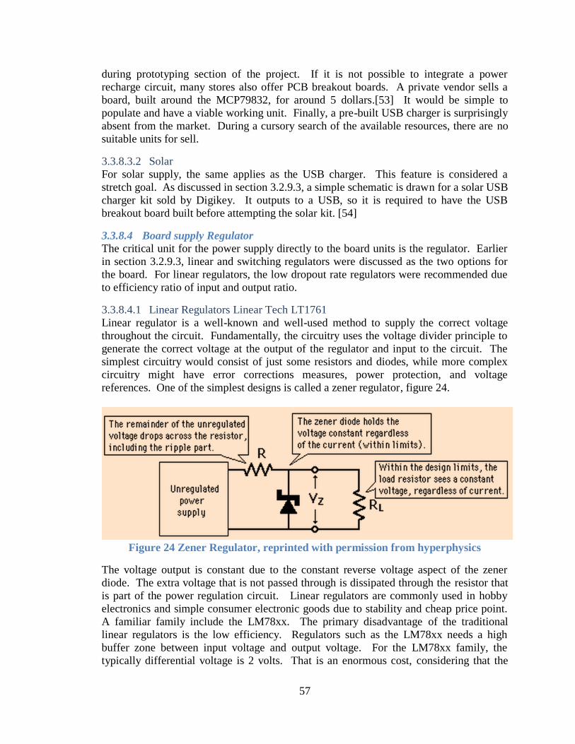
57
during prototyping section of the project. If it is not possible to integrate a power
recharge circuit, many stores also offer PCB breakout boards. A private vendor sells a
board, built around the MCP79832, for around 5 dollars.[53] It would be simple to
populate and have a viable working unit. Finally, a pre-built USB charger is surprisingly
absent from the market. During a cursory search of the available resources, there are no
suitable units for sell.
3.3.8.3.2 Solar
For solar supply, the same applies as the USB charger. This feature is considered a
stretch goal. As discussed in section 3.2.9.3, a simple schematic is drawn for a solar USB
charger kit sold by Digikey. It outputs to a USB, so it is required to have the USB
breakout board built before attempting the solar kit. [54]
3.3.8.4 Board supply Regulator
The critical unit for the power supply directly to the board units is the regulator. Earlier
in section 3.2.9.3, linear and switching regulators were discussed as the two options for
the board. For linear regulators, the low dropout rate regulators were recommended due
to efficiency ratio of input and output ratio.
3.3.8.4.1 Linear Regulators Linear Tech LT1761
Linear regulator is a well-known and well-used method to supply the correct voltage
throughout the circuit. Fundamentally, the circuitry uses the voltage divider principle to
generate the correct voltage at the output of the regulator and input to the circuit. The
simplest circuitry would consist of just some resistors and diodes, while more complex
circuitry might have error corrections measures, power protection, and voltage
references. One of the simplest designs is called a zener regulator, figure 24.
Figure 24 Zener Regulator, reprinted with permission from hyperphysics
The voltage output is constant due to the constant reverse voltage aspect of the zener
diode. The extra voltage that is not passed through is dissipated through the resistor that
is part of the power regulation circuit. Linear regulators are commonly used in hobby
electronics and simple consumer electronic goods due to stability and cheap price point.
A familiar family include the LM78xx. The primary disadvantage of the traditional
linear regulators is the low efficiency. Regulators such as the LM78xx needs a high
buffer zone between input voltage and output voltage. For the LM78xx family, the
typically differential voltage is 2 volts. That is an enormous cost, considering that the

58
entire circuit package needs to run around 3.6 volts and every volt added could mean
bulkiness and weight in package. In addition, any extra voltage is dissipated as heat,
creating a thermal threat to the operation of the package and to the baby’s skin. The
thermal and voltage differential can be solved by using a low dropout linear regulators.
Nowadays, IC makers offer linear regulators with low differential with input/output, low
noise, and a fast transient response. Some of options include such devices such as Linear
Technology’s LT1761, an option with a low dropout voltage of 300 mV at 100mA of
output current. In a typical application, the input/output differential is a mere 0.4V. This
is a 500% improvement over the LM78xx family. What is more, the quiescent current
for this unit is also very low at 20 . The shutdown Quiescent current is less than 1 . The Figure is configured to 5 volts output. This voltage regulator comes in a host of
different voltage levels, including 1.2V, 1.5V, 1.8V, 2V, 2.5V, 2.8V, 3V, 3.3V, and 5V.
While the TPS62740 is the ideal regulator for the project, a backup regulator has been
chosen in the event TPS62740 does not work as promising as it looks on paper. As
discussed earlier in the section on regulator background, switching regulator, due to the
frequency at which it opens and closes a switch, can interfere with radio frequency
signals. In the case that the signal is noisy and the problem is determined to originate
from the switching regulator, a possible replacement linear regulator will be used. The
recommended linear regulator is the LT1761-3.3. According to the datasheet on Linear
Technology’s website, this is a low drop out voltage regulator with low noise design.
Figure 25 shows the curve of typical drop out voltage in regards to the differing output
currents. For Baby Peas, output current can range from 50mA to over 100mA. At the
lower end of that spectrum, 250mW differential will be required from the input to the
output. While not ideal, this is very low for a linear regulator. At the higher end of the
spectrum, the cost differential is higher. This is why the linear regulator is the backup
choice. Despite the cost, the LT1761 is still lower than most of the competitors.
Figure 25 Typical Dropout Voltage approximation diagram for LT1761. Created by
Xin Tong in MS Excel
The quiescent current is at 20uA and comes in a static voltage select package. In
addition, throughout the course of usage, the quiescent is controlled to near 20uA.

59
Figure 26 Typical Application for LT1761. Created by Xin Tong in NImultisim
3.3.8.4.2 Switching Regulators Texas Instruments TPS62740
The second option for power regulation is switching, or switched-mode power supply. In
this case, the power supply is switched on and off in a swift pace, outputting an average
supply voltage. The switching regulator, such as the one shown in Figure 27, control the
gate using a certain frequency. The amount of power going through is determined by the
amount of time the switch is closed. The output voltage depends on how much voltage is
at Vin, and the switch duty cycle.
Figure 27 Simplified Switching Regulator. Created by Xin Tong in NImultisim
The controlling gate of the switching regulator is usually a transistor or a thyristor. In
addition, extra components are needed to make a circuit function as a useful power
supply. Rectifying diodes and inductors help the output capacitor with providing a steady
ripple free output. Figure 27 shows one such configuration.
Because there is no constant supply of power, this helps to prevent the waste of power.
The advantages of switching regulators are efficiency (longer battery life and less heat
dissipation) and size. While switching regulators often require more components than
linear regulators, the fact that switching can forgo the heat sinks that are a staple of linear

60
regulators. Some of the disadvantages of switching are a higher cost compared to linear
and the introduction of more noise. In addition, switching regulators often require a little
more complexity in circuitry, and will need inductors to act as an energy storage element
and external diodes. The disadvantages of noise can be ameliorated by using families of
ultralow noise regulators. For example, Linear Technology offers packages such as the
LT1533. Designed specifically for sensitive instrumentation measurements and medical
devices, this regulator is designed so that the noise generated by the frequency of the
switch duty cycle will not interfere with other modules on the board. TI’s Bluetooth
sensor tag uses a switch regulator, the TPS62730.
Key Features
Input Voltage Range from 1.9V to 3.9V
Typical 30 nA Ultra Low Power Bypass Mode
Supports sleep and low power modes on CC2541
Typical 25 µA DC/DC Quiescent Current
DC/DC converter connected via typical 2.1Ω Bypass switch to battery
The TPS62730 is a step-down DC/DC buck converter. Figure 28 below shows the
typical battery current of the CC2540 model versus the voltage of the battery. The
TPS62730 minimizes the current drawn from the battery during both transmission and
reception modes. The graph shows a clear reduction of battery current used as the
voltage increases. This decrease in current allows the prolonged use of the powered
device in transmission mode. A long battery life is essential to the use of the project.
The longer the battery can be powered without recharge, the more useful and convenient
the device will actually be. This ensures the child will be monitored through a longer
uninterrupted period of time, where parents do not have to constantly worry about how
much battery life is left. This device supports Lithium powered battery chemistries such
as LiSOCl2, LiSO2, LiMnO2, and other two cell alkaline batteries.
Figure 28 Current vs Voltage with TPS62730, Reprinted without alteration with
permission from Texas Instruments

61
The Figure 29 below show the relative current consumption during data transmission.
The bottom axis is labeled as supply voltage increasing from left to right. The left
vertical axis is labeled as current in mA increasing upward. The blue bar shows the
current consumption at its corresponding voltage without using the TPS62730 DC/DC
converter. The red bar shows the current consumption with the CC2541 connected to the
TPS62730 DC/DC converter in ON mode. For increasing voltage, the current
consumption with the DC/DC converter on steadily declines. The vertical axis on the
right side is labeled for percentage of current savings. This is the percentage of current
decrease depicted in the red bar with respect to the blue bars. The current savings
steadily increases with increasing voltage. This indicates that there is up to 37 percent
decrease in current in transmission mode, and up to 35 percent decrease in current in
receiving mode. This overall decrease in current in both modes will lead to a much
longer battery life as compared to the blue bars, which show an increase in current with
its associated increase in input voltage. It stands to reason that without using the
TPS62730, the battery life will be approximately one third shorter than the alternative.
While the TPS62730 is used in TI’s sensor tag, the regulator recommended for this
project is the TPS62740.
Figure 29 Current Consumption in TX and RX, used with permission from Texas
Instruments
Figure 30 below shows an example application of the TPS6270 connected to a CC2540
(similar to the CC2541). The figure shows how the two devices are probably connected
in the CC2541 layout. The power-down signal is passed from the P1.2 MUX to the
TPS62730 ON/BYP input pin. In this way, the mode selection of the TPS62730 is
dictated by the microcontroller programming. If the ON/BYP pin is low, the TPS62730
is in its ultra-low power bypass mode. In this mode, VIN is directly connected to VOUT
through an internal Bypass switch and consumes only 30 nA typical input current. The
output of the buck converter is connected to the battery VIN. When the pin is high the
transition from Bypass mode to DC/DC converter operation is enabled. This transition
state is to reduce the amount of ripple voltage to zero or near zero and is regulated by

62
output capacitors (shown in figure) and internal decoupling capacitors. Once the
capacitors are discharged sufficiently and internal comparators recognize the increase in
input voltage, the bypass switch is deactivated, allowing normal operation of the DC/DC
step down converter.
Figure 30 TPS - CC2540 Reference Design. Reprinted without alteration with
permission from Texas Instruments

63
3.3.8.4.2.1 Pin Functions
The pin descriptions, contained in Table 17, for the TPS62730 are helpful references to
understanding exactly how the chip will be connected to the CC2541. The functional
block diagram is also more easily understood knowing the pin functions.
Pin I/O Description
Name NO
VIN 3 PWR Power supply pin
GND 4 PWR Ground supply pin ON/BYP 5 IN Mode Selection pin. Pulling pin low forces device into ultralow
power bypass mode. The output of the DC/DC converter is connected to VIN via an internal bypass switch. Pulling this pin to high enables the DC/DC converter operation. This pin must be terminated and is controlled by the system.
SW 2 OUT This is the switch pin is connected to the internal MOSFET switches.
VOUT 6 IN Feedback Pin for the internal feedback divider network and regulation loop. The internal bypass switch is connected between this pin and VIN
STAT 1 OUT This is the open drain status output with active low level. An internal comparator drives this output. The pin is high impedance with ON/BYP = low. With ON/BYP set to high the device and the internal VOUT comparator becomes active. The active low STAT pin indicates if the DC/DC regulator is settled and the output voltage above the VTSTAT threshold. If not used, this pin can be left open. Table 17 TPS62730 Pin Description [23]
Figure 31 below depict the efficiency versus Input Voltage (left) and Output Current
(right) of the TPS62730 in ON mode (ON/BYP = high). The trends for the efficiency of
the chip versus output current shows positive correlation between output current and total
efficiency for various input voltages. Although there is an expected dip in efficiency for
larger input voltages, all voltages in the operating range are above 85 percent, even
towards larger output current values. The orange graph line shows the chip operating in
bypass mode. In bypass mode, the efficiency peaks at almost 100 percent from 1-10 mA.
This makes sense because in bypass mode the voltage is going straight from VIN to
VOUT through the bypass switch. The right figure shows the efficiency with respect to input voltage. The efficiency once again increases for larger values of output current.
However, there is a slight negative correlation as the input voltage increases. The
efficiency still manages to stay about 80 percent from 1mA to 100mA. At high input
voltages, the 100mA ends up being the most efficient.

64
Figure 31 TPS62730 Efficiency Charts, Reprinted without alteration with
permission from Texas Instruments
Figure 32 below illustrates the internal components of the TPS62730 with a functional
block diagram. The ON/BYP input on the left side determines the running mode. When
the pin is low, it shows a low voltage to the AND gate, which in turn gives a low signal.
That bypass signal shows up on the switch in the upper right corner labeled “/BYPASS”.
In this mode, the signal from VIN goes directly to VOUT. The signal from VOUT is fed
back to the error comparator through the error feedback network. When the ON/BYP pin
is high, the buck converter is active. The STAT pin is the status pin used for monitoring
the working mode of the TPS62730. When bypass mode is active, the ON/BYP pin is set
to low. The STAT pin should then also read as high impedance. When the DC/DC
regulator is on, the ON/BYP pin is set high. The STAT pin should read high as well in
this setting. This pin is modulated by the internal VIN comparator as seen in the
functional block diagram. Because STAT is simply an observation pin, it is optional to
connect this pin. However, most of its use can come in the development and testing
process. The status pin can be connected and monitored to ensure the components are
working properly.

65
Figure 32 TPS62730 Functional Block Diagram, Reprinted without alteration with
permission from Texas Instruments
TPS62740 is the recommended voltage regulator for this project due to its compact size
and power parameters. In addition, the family of TPS627XX has proven suitability in a
design with the CC2541; this is the regulator that the TI sensor tag developmental kit
uses. That kit is using a TPS62730, a lower voltage regulator than the TPS62740.
TPS62740 has a new DCS-Control feature that incorporates a tiny inductor and output
capacitor to improve efficiency during times of low power usage. DCS-Control, or Direct
Control with Seamless Transition into Power Save Mode) is a topology trademarked by
Texas Instruments and this topology was developed to aid power density and efficiency.
This Direct Control with Seamless Transition into Power Save Mode incorporates AC
control loop, Voltage feedback loop, and internally compensated regulation network.
The AC control loop “takes information about output voltage changes and feeds it
directly to a fast comparator stage for immediate response to dynamic load changes”.[x]
This feature, in addition to the voltage feedback look feature, which helps to sharpen DC
load regulation, allows for a clean and stable output. In addition the internal
compensated regulation network is a great buffer package that is able to dynamically
stabilize with external components. The DCS-control topology switches between pulse
width modulation and power save mode for efficiency for both medium to heavy loads
(Pulse Width Modulation) and light loads (Power Save Mode). Figure 33 shows the
efficiency gains the new TPS62740 offers at low output current.

66
Figure 33 Extension Range of TPS62740 Efficiency Down to 0.01mA. Reprinted
with the courtesy of TI documentation on TPS62740
The TPS62740 has improved on the transition between the two modes and decreased
voltage ripple and random jitter.[55] The older direct current to direct current regulators,
which switched between the two modes by using physically separated blocks for the two
different modes, usually set the pulse width modulation mode as default due to the
voltage ripple and random jitter. However, this move cost the regulator in efficiency. In
the new TPS627XX family, the pulse width modulation and power save mode blocks are
integrated into a “single building block”, which provides a “seamless transition between
PWM and Power Save Modes”. [55] Due to the architecture of the blocks and internal
regulation network, the quiescent current is 360nA during typical operations. Quiescent
current is an important consideration in the project due to the way the Baby peas unit
operates. Total battery life comes from both the load current and quiescent current, or
standby current. The portability of Baby peas faces a huge compromise if the quiescent
current is large. Figure 34 shows the different quiescent current with differing voltage in.

67
Figure 34 Quiescent Current During Differing VIN. Reprinted without alteration
with permission from Texas Instruments.
The maximum operating current goes to 300 mA. At 10uA, the efficiency touches 90%.
In order to prevent ripple noise from propagating through the circuit, TPS62740 also
“features low output ripple voltage and low noise with small output capacitor”.[55] The
scheme behind this features is the dynamic operation of the no ripple mode operation. In
the past, as the battery source start to get close to the output voltage on the regulator,
certain characteristics such as ripple voltage start to increase. To stop this, the TPS62740
uses a 100% mode operation at this point to lessen the impact of the ripple voltage;
basically the regulator changes to a linear like device, and “stops switching and the
output is connected to the input voltage directly from the battery”.[55] Figure 35
demonstrates this principle. The input and output form a y = kx relationship at the lower
voltages, while at higher voltages, the out is a constant. The x value is the input value,
and the output voltage is the output value, while the k value represents a constant
multiplier. At the lower voltages, this just means that what comes into the regulator is
output on the other side at an almost 100% mode. At higher voltages, the regulator starts
to function like a traditional switching regulator, and regulate the incoming voltage down
to the correct output voltage.

68
Figure 35 100% Mode Transition for Vout of 2.1V. Reprinted without alteration
with permission from Texas Instruments.
Intended to run from rechargeable Li-Ion batteries, this unit can have an input range of
Vin from 2.2 V to 5.5 V. The additional nicety about this unit is the different levels of
voltage output. Ranging from 1.8V to 3.3V, four voltage select pins can be pulled high in
different configurations in order to output differing voltages in 100mA steps. Table 18
shows the different voltage selections levels and pin configuration logic for the Baby
Peas project

69
Device VOUT VSEL4 VSEL3 VSEL2 VSEL1
TPS62740
1.8 0 0 0 0
1.9 0 0 0 1
2.0 0 0 1 0
2.1 0 0 1 1
2.2 0 1 0 0
2.3 0 1 0 1
2.4 0 1 1 0
2.5 0 1 1 1
2.6 1 0 0 0
2.7 1 0 0 1
2.8 1 0 1 0
2.9 1 0 1 1
3.0 1 1 0 0
3.1 1 1 0 1
3.2 1 1 1 0
3.3 1 1 1 1
Table 18 Different Voltages Based on the Selection of the Pins, with the Highlighted
Numbers as the Chosen for Baby Peas
This feature is great due to the scalability for future boards. While current modules on
the Baby Peas require voltages around 3V, the future iterations or different models could
require less or more voltage. For example, the pulse-ox unit raises the voltage
requirement for the entire unit. The accelerometer and temperature sensors hover around
2.75 for voltage requirement, but the pulse-ox require a 3-3.3V input. If a baby peas unit
was built only around the accelerometer and temperature, the regulator could be
configured to select only pins VSEL 4 and VSEL2. That could length the battery life by
a magnitude. The ability of the pin select allows the designers to choose the best output
voltage for the system. Currently for the Baby Peas unit, all the VSEL pins, VSEL1
through VSEL 4, are going to be pulled high, so the output voltage of the TPS62740 is
going to be at 3.3. The overall efficiency of the regulator TPS62740 when all the VSEL
pins are pulled up for an output of 3.3V is given in figure 36. As you can, with the button

70
batter LIR2477, the efficiency curve lies somewhere between the green and orange curve.
The LIR2477 outputs 3.7 potential. This is close to a 95% percent efficiency, meaning
longer battery life and less thermal dissipation.
Figure 36 Efficiency of Regulator with Different Output Current. Reprinted
without alteration courtesy of Texas Instruments
3.3.8.5 Requirements
As discussed above, the either a linear or a switching regulator can be used to augment
the power coming in from a battery. Also discussed prior, the battery unit can be either
coin packaging or a super capacitor; either option could theoretically work. It is best to
test to see which option does best in the field.

71
Requirements for the subsystems:
MPU - 6050
Operating Current Voltage Min Voltage Max
Gyroscope +
Accelerometer + DMP
3.9 mA 2.375 V 3.46 V
Gyroscope +
Accelerometer
3.8 mA 2.375 V 3.46 V
Gyroscope + DMP 3.7 mA 2.375 V 3.46 V
Gyroscope only 3.6 mA 2.375 V 3.46 V
Accelerometer only 500 2.375 V 3.46 V
Table 19 Normal Operating Current for MPU-6050
Other modules
Current Max Voltage Min Voltage Max Recommended
Voltage
CC2451
-0.3 3.9 2 to 3.6
AFE4490
50mA 5.25V 7V 3-3.2
Tmp006
10mA 2.2 7V
Table 20 Normal Operating Requirements for Modules
3.3.8.6 Schematics for TPS62740
Figures 37 through 39 shows the schematic and package views of TPS62740 regulator.
It is important to know the size of the package, including height, due to the unforgiving
size of the entire unit. In addition, figure 40 shows the thermal pad of TPS62740.
Special care should be made when soldering the thermal pad as it acts as the heat sink for
the regulator and any defectiveness in contact could mean catastrophic consequences for
the entire unit. A figures not created in Eaglesoft are courtesy of Texas Instrument’s
datasheet for the TPS62740

72
Figure 37 Configuration for integration of TPS62730 with the CC2541. Created
using Cadsoft Eagle
Figure 38 Shows the Package Size and Pin Size of TPS62730

73
Figure 39 Shows the Seating Plane and Height of TPS62730
Figure 40 Shows the Thermal Pad for TPS62730

74
4 Project Hardware and Software Design Details
4.1 Hardware
The Hardware high level System block diagram shown above in Figure 41 gives a nice
overview of each subsystem and on how each individual sub-system will interact with
each other. The Battery Re-charge section will serve as both as a re-charge circuit for the
battery and also a protection circuit for the system not allowing the system to be in
operation during re-charge mode. The Re-chargeable battery will be a simple Coin Cell
re-chargeable battery feeding into the DC-DC voltage Regulator circuit. The Voltage
regulator circuit will provide isolation to the rest of the circuit along with power to each
sensor and the RF/Microcontroller module. Each sensor will interact with the infant in
some way and transmit data over either SPI or I2C to the CC2541. The CC2541 will
process the data received and transmit data packets to the user display device. The
following sections will dive deeper into the hardware design of each subsystem providing
schematics for each section with a final schematic of the overall system.
Figure 41 Baby Peas System Hardware Block Diagram
CC2541 Microcontroller
Bluetooth BLE v4.0 RF
module circuit
BLE V4.0
compatible display
device
Heart Rate / Blood
Oxygenation Sensor
Circuit
Body Position
Sensor Circuit
Skin Temperature
Sensor Circuit
Battery Re-charge
and protection
circuit
Re-chargeable
Battery circuit
DC-DC regulator
circuit
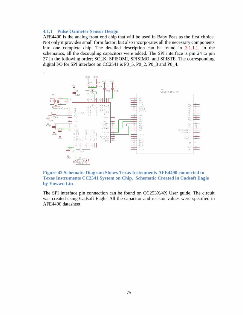
75
4.1.1 Pulse Oximeter Sensor Design
AFE4490 is the analog front end chip that will be used in Baby Peas as the first choice.
Not only it provides small form factor, but also incorporates all the necessary components
into one complete chip. The detailed description can be found in 3.1.1.1. In the
schematics, all the decoupling capacitors were added. The SPI interface is pin 24 to pin
27 in the following order; SCLK, SPISOMI, SPISIMO, and SPISTE. The corresponding
digital I/O for SPI interface on CC2541 is P0_5, P0_2, P0_3 and P0_4.
Figure 42 Schematic Diagram Shows Texas Instruments AFE4490 connected to
Texas Instruments CC2541 System on Chip. Schematic Created in Cadsoft Eagle
by Yowwu Lin
The SPI interface pin connection can be found on CC253X/4X User guide. The circuit
was created using Cadsoft Eagle. All the capacitor and resistor values were specified in
AFE4490 datasheet.

76
4.1.2 Body Position Sensor Design
For the body position sensor the IMU-6000 was chosen from Invensense. Figure 43
below block diagram of the connections between the MPU-6000 and the CC2541
Microcontroller
Figure 43 Block Diagram for Body Position Sensor
From Figure 43 we see the data transfer and communications for the device will be using
I2C. The SDA line is where the data will move through serially. The SCL line is the
clock and CS line is used for chip select. The CC2541 I2C lines for SCL and SDA are
hard line wired to Pins 2 and 3 respectively. The chip select line was chosen to be one of
the digital I/O lines running from the CC2541. Pin 8 is listed as port 1.2 on the CC2541
and can be used as the chip select line. V_REG will be the input voltage line from the
regulator circuit and GND is connected to system ground. Figure 44 is the schematic
diagram layout for the MPU-6000.
Pin 24 SDA
Pin 23 SCL
Pin 8 CS
SDA Pin 3
SCL Pin 2
CS Pin 8
CC2541
SCL Pin 2
MPU-6000
SCL Pin 2
V_REG
Pin
24 V
DD
Pin
23 G
ND
GND

77
Figure 44 Schematic Diagram for Position Sensor Utilizing Cadsoft Eagle. Circuit
created by Christopher Ramirez
4.1.3 Skin Temperature Sensor Design
For the Skin Temperature Section the TMP006 was chosen because of its ability to read
temperature without having to make contact with the infant. Figure 45 below is the block
diagram of the connections of the TMP006 with the CC2541.
Figure 45 Block Diagram for Skin Temperature Sensor
Pin C3 SDA
Pin B3 SCL
Pin C2 DRDY
SDA Pin 3
SCL Pin 2
CS Pin 7
CC2541 TMP006
V_REG
SCL Pin
Pin
A3 V
DD
Pin
A2 G
ND
GND
SCL Pin

78
From Figure 45 the data transfer lines are utilizing I2C as well communications between
the TMP006 and CC2541. The only difference is the designation name for chip select on
the TMP006 which is labeled as instead of CS. The over line means the line is active low. Pin 7 on the CC2541 is another digital I/O line. It is port P1.3 and is used for
toggling the chip select line. Figure 46 below is the schematic diagram for the TMP006
created in CADsoft EAGLE.
Figure 46 Schematic Diagram for Temp Sensor Utilizing Cadsoft Eagle. Circuit
created by Christopher Ramirez
If the TMP006 proves to be difficult to work with will will have enough space on the
PCB to also utilize the TMP103 by Texas Instruments. Texas Instruments TMP103 is a
four ball wafer chip-scale package features two-wire interface digital output temperature
sensor that may be used for Baby Peas monitor. The simple and straight forward design is
easy to integrate with Texas Instruments CC2541. The interface is I2C and SMBus
protocol. In the schematic diagram shown in Figure 47, the supply voltage 3.6 V is
connected to V+ port and ground has been connected. The resistor is recommended to
have value equal or less than 5 K Ohm and capacitor in parallel value of greater or equal
to 10 nanofarad. Because of the simplicity nature of TMP103, it has low noise level. An
additional RC filter may further reduce the noise level.

79
Figure 47 Schematic Diagram Shows Texas Instruments TMP103 connected to
Texas Instruments CC2541 Bluetooth System on Chip. Schematic diagram created
with Cadsoft Eagle by Yowwu Lin.
4.1.4 Communications / Microcontroller Design
Due to the nature of the Bluetooth Module and Microcontroller being on the same
integrated circuit the communications design and microcontroller design specifications
and characteristics will be discussed and explained in the same section.
4.1.4.1 Communications
The CC2541 was decided to be the Bluetooth Low Energy RF module used by Baby Peas
project team. As in all RF designs careful consideration must be adhered to during the
layout process to ensure proper impedance matching is upheld on the output RF pins of
the CC2541. Figure 48 shows the block diagram for the configuration of the
communications section of the Baby Peas project.
Data Inputs From
Sensors Via SPI or
I2C
VCC
Debug Header
used for
Programming /
Troubleshooting
CC2541 RF Output
Impedance
matching
network
32.768 kHz
Oscillator
32MHz
Oscillator
Figure 48 Block Diagram for CC2541

80
From Figure 48 one can observe the CC2541 is the heart of the system because it handles
both the RF and Microcontroller aspects of the baby peas design. Figure 49 is the
schematic design for the CC2541 and will be discussed in the following sections for both
the RF and Microcontroller aspects of the project.
Figure 49 Schematic design for the CC2541 Communications / Microcontroller.
Created in Cadsoft Eagle by Christopher Ramirez
From Figure 49 we see that most of the capacitors connected in parallel have to do with
low and high frequency noise filtering. This is a critical portion of the project since a
switching regulator is used. RF devices need clean power to be able to transmit data bits
efficiently. Noise on the device can effect receiver sensitivity and cause degradation of
the system. The impedance matching network was chosen to be a murata balun which
was suggested for ease of implementation to guarantee proper impedance matching to 50
ohm so the transmit and receive power levels are accurate with the ones provided on the
data sheet. Discrete inductors and capacitors can be used also if the murata balun proves
to be difficult to install. The antenna used will be constructed within the microstrip line
itself. Design details for the microstrip line are provided by Texas Instruments. The
remaining items on the schematic are talked about extensively in the following sections

81
4.1.4.2 Microcontroller CC2541 Design characteristics
The CC2541 was determined to be the microcontroller with the specifications which is
best suited for the Baby Peas peripheral sensor system. The advantages to using this
particular model include the Bluetooth module on the same chip, large amount of
memory, and high efficiency through the flexible power modes. The microcontroller
itself supports enough flash memory and is fast enough to successfully handle the
processes that are required of it. The number of input/output ports is also a sufficient
number and resolution to support the sensors to be used. The development kit comes
with examples of how to program biomedical devices, which will be a valuable resource
during the building phase.
4.1.4.2.1 Electrical Characteristics
The typical current consumption of the cc2541 in different settings are as follows. In
standard and RX mode with no peripherals active and low MCU activity, the current
consumption is typically 17.9 mA. If the standard mode is switched to high-gain mode,
keeping everything else the same, the core consumes 20.2 mA. In TX mode and -20
dBm output power the core current is 16.8 mA. At 0 dBm, it is 18.2 mA. For general
low MCU activity, the 32 MHz XOSC is running with limited flash access. No radio or
peripherals are active and RAM cannot be accessed. The current consumed is 6.7 mA.
Power mode 1 implies the following: the digital regulator is on, the 16-MHz RCOSC and
32-MHz crystal oscillator is off, the 32.768-kHz XOSC, POR, BOD and sleep timer is
active, RAM and register data is retained. The current consumed is 270 μA. Power
mode 2 implies the following: the digital regulator is off, the 16-MHz RCOSC and 32-
MHz crystal oscillator is off, the 32.768 kHz XOSC, POR, and sleep time are active,
RAM and register data is retained. The current consumed is 1 μA. Power mode 3
implies the following: the digital regulator is off, there are no active clocks, the POR is
active, RAM and register data is retained. The current consumed is 0.5 μA. Peripheral
current usage of the cc2041 adds to the core current when the peripheral unit is activated.
The analog-to-digital converter uses 1.2 mA when converting. Timer 1-4 runs with the
32-MHz XOSC. Timer 1 uses 90 μA, Timer 2 90 μA, Timer 3 60 μA, and Timer 4 70
μA. The Sleep timer includes the 32.753-kHz RCOSC and uses 0.6 μA. The output
power of the device is associated with a typical current consumption. When the output
power is 0 dBm, the current consumption is typically 18.2 mA. At -20 dBm, the current
consumption is typically 16.8 mA.
4.1.4.2.2 Current Consumption with TPS62730
In RX mode, standard mode, with no peripherals added and low MCU activity at 1 MHz,
the current consumption is 14.7 mA. In RX mode and high-gain mode, keeping
everything else the same, the current consumption is 16.7 mA. In TX mode at -20 dBm
output power, with no peripherals active and low MCU activity at 1MHz, the current
consumption is 13.1 mA. In TX mode at 0 dBm, keeping everything else constant, the
current consumption is 14.3 mA. The current used in both transmit and receive modes
are relatively small. It follows that the larger the signal, the more power is required to
power the device

82
4.1.4.2.3 General Characteristics
The wake-up and timing characteristics are as follows. Power 1 means the digital
regulator is on and the 16-MHz RCOSC and 32-MHz crystal oscillator is off. The start-
up of the 16-MHz RCOSC to active mode takes 4 μs. In Power mode 2 or 3, the digital
regulator, 16-MHz RCOSC and 32-MHz crystal oscillator are off. The start-up of the
regulator and 16-MHz RCOSC to active mode takes 120 μs. The timing of active mode
to TX or RX are as follows: with the 16-MHz RCOSC on and 32-MHz XOSC off, 500
μs; with the 32-MHz XOSC initially on, 180 μs.
4.1.4.3 CC2541 Block Diagram
Modules can be divided into three categories: CPU-related modules; Power, test, and
clock distribution; radio-related modules. The CPU related modules refer to the 8051
core architecture and the memory associated with the 2541. This includes RAM, ROM,
flash memory, and the memory arbitrator. Data buses are also grouped together in this
category. Power, test, and clock distribution modules are lumped together. This refers to
the VDD pins, debug pins, crystal oscillator pins, and timers. The radio-related modules
are the RF pins that receive and transmit wireless data to other peripherals. The Block
Diagram of the CC2541 can be referenced in Figure 49 for the RF portion of the project
and Figure 50 for microcontroller aspects of the project
4.1.4.4 CPU and Memory
The CPU is the source of all essential mathematical data manipulation that occurs
throughout the microcontroller. The data is then sent out to its appropriate destination as
designated by the coding. The Direct Memory Access (DMA) is the component used to
actually move the data around, thus enabling the CPU to concentrate on other processes.
The CPU and DMA are connected by the Memory Arbiter. Data that must be reserved
for later is stored in memory, where it can be later accessed if needed for other
miscellaneous tasks. Ultimately, the success of the project depends on efficient use of the
CPU and memory modules. (Referenced to Figure 50)
8051 CPU core o Single-cycle 8051-compatible core
o Three different memory access busses (SFR, DATA, and CODE/XDATA)
o Debug interface
o 18-input extended interrupt unit
Memory arbiter o Connects CPU and DMA controller with physical memories and all
peripherals through SFR bus
o Four memory-access points
SRAM
Flash memory
XREG/SFR registers
o Responsible for performing arbitration and sequencing between
simultaneous memory accesses to the same physical memory
SFR bus
o Connects hardware peripherals to memory arbiter
o Provides access to radio registers

83
8-KB SRAM o Maps to DATA memory space and parts of the XDATA memory spaces
o Ultralow-power non-volatile SRAM (power mode 2 and mode 3)
128/256 KB flash block
o In-circuit programmable non-volatile program memory
o Maps into CODE and XDATA memory spaces
4.1.4.5 Peripherals
The peripheral modules support the core CPU and memory modules in running the
microprocessor by controlling the flow of data to or from the central components. The
DMA, Interrupt, and Input/Output controllers all administrate the accurate transfer of
data within memory and with external sources. The timers specifically control the timing
of the system, providing an ordered sequential structure to the various processes that take
place. The rest of the peripheral modules, including the UART, I2C, SPI, and AES
components, enable the communication of data between devices. The project will be
exchanging data between components, so these peripheral modules will be used
extensively. (Referenced to Figure 50)
DMA controller o Five channel
Trigger, Priority, Transfer mode, Addressing mode, source and
destination pointers, and transfer count
Each channel is configured with DMA descriptors
Can be located anywhere in memory
o Accesses data using XDATA memory space, allowing access to all
physical memories
o Many hardware peripherals are used with the DMA controller
Interrupt controller o Controls 18 interrupt sources
o Further divided into 6 interrupt groups
o 4 interrupt priorities
o I/O and sleep timer interrupt requests work when the CC2541 is in power
mode 1 or 2 (sleep mode) to bring it into active mode
Debug interface o Two-wire serial interface
o In-circuit debugging
o Capable of erasing or programming the entire flash memory
o Stop/start execution of user program
o Execute 8051 core instructions
o Set code breakpoints
o Single-step through code instructions
I/O controller
o Controls all general purpose I/O pins
o CPU assigns control of pins to peripheral modules or software
o Assigns input or output configuration of pins
o Connects pullup/pulldown resistors

84
o Peripherals can choose between two I/O pin locations
Sleep Timer o Ultralow-power timer
o Uses either external 32.768 kHz crystal oscillator or internal 32.753-kHz
RC oscillator
o Runs continuously in all modes except power mode 3
Watchdog Timer
o Allows the CC2541 to reset itself
Timer 1 o 16-bit timer
o Timer/counter/PWM functionality
o 16-bit period value
o 5 individually programmable counter/capture channels
Timer 2 o 40-bit timer
o 16-bit counter and 24-bit overflow counter
o 40-bit capture register to record start and end of transmission
o Two 16-bit output compare registers and two 24-bit overflow compare
registers to record start of RX/TX or general interrupts
Timer 3 and Timer 4 o 8-bit timers
o Timer/counter/PWM functionality
USART 0 and USART 1
o Can be used as either SPI master/slave or UART
o Provides double buffering
AES encryption/decryption o Uses AES algorithm with 128-bit keys
o Supports ECB, CBC, CFB, OFB, CTR, and CBC-MAC
ADC o 7-12 bit resolution from 30-kHz to 4-kHz, respectively
o Single-ended or differential
o Reference voltage can be internal, AVDD, or single-ended/differential
external signal
I2C
o Digital peripheral connection with two pins
o Supports both master and slave operation
Analog Comparator o Enables applications to wake up from Power Mode 2 or Power Mode 3
based on an analog signal
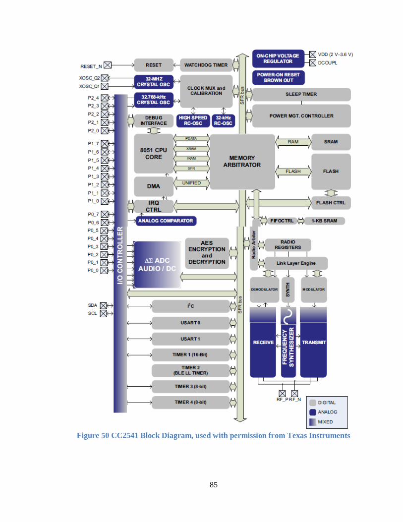
85
Figure 50 CC2541 Block Diagram, used with permission from Texas Instruments

86
4.1.4.6 Application information CC2541
The schematic configuration of the CC2541 is shown again in Figure 51. The remaining
sections walkthrough the different uses of the pins which have not be covered yet.
Figure 51 Schematic design for the CC2541 Communications / Microcontroller.
Created in Cadsoft Eagle by Christopher Ramirez
4.1.4.6.1 Power configuration
A 2 to 3.6-Volt power supply is connected to pin 10, 21, 24, 27, 28, 29, 31, and 39. Each
of these pins are a DVDD or AVDD pins which are the Digital voltage inputs and Analog
voltage inputs. These can be tied together because a separate digital voltage line is not
being used in the Baby Peas project. XOSC_Q1 Pin 22, XOSC_Q2 Pin 23 - These two
pins are attached to an external 32 MHz oscillator. This oscillator is used to clock the
central operations of the CC2541 hardware. RBIAS Pin 30 – The resistor R301 is
attached from pin 30 to ground. This resistor is used for internal biasing. The biasing
resistor will add voltage offset where needed and stabilize transistor current to avoid
saturation or cut-off of electrical signals. If a biasing resistor was not connected to this
position, the voltage applied to the internal components may not be constant, resulting in
unintended outputs. The R301 resistor is a precision resistor ±1% at 56 kΩ. Pins RF_P
Pin 25 and RF_N Pin 26 connect the CC2541 internal components to the electrical
signals provided by the RF network and the Bluetooth modules. RF_P deals with the
positive component of the radio signal either being received or broadcasted. RF_N deals
with the negative component of the radio signal being received or broadcasted. These

87
two pins are extremely important to layout correctly to adhere to impedance matching
characteristics which arise in mircrowave circuits. P2_3/XOSC32K_Q2 (Pin 33) and
P2_4/XOSC32K_Q1 (Pin 34) pins are attached to an external 32.768 kHz oscillator.
This oscillator is used as a clock for the input/output pins and receives information from
the high level clock MUX and calibration circuits. DCOUPL Pin 40 – A capacitor is
attached from this pin to ground. It acts as a decoupling capacitor for the CC2541. A
decoupling capacitor is used to filter low frequency noise out of the circuitry. Without a
capacitor at this pin, the internal components of the microcontroller would see more
noise, potentially causing a slowdown of processing speed or incorrect information being
passed through the system.[25]
4.1.4.6.2 SPI bus AC Characteristics of CC2541
A SPI bus will be needed for the implementation of the AFE4490 pulse oximetry
circuitry and Debug capabilities. It is important to understand how the SPI bus operates
in order to successfully program the hardware. The SPI bus also allows for scalability if
more sensors are desired to be added to the Baby peas’ peripheral device. The AC
characteristics of the SPI bus are the timing cycles of the bus during data transmission.
The Serial Peripheral Interface bus specifies four logic signals:
SCK – Serial clock (output from master)
MOSI – Master output, slave input (output from master)
MISO – Master input, slave output (output from slave)
SSN – slave select (active low, output from master)
Figure 52 below shows the direction of signals in the SPI connection from one master
device to multiple independent slave devices. The SPI Master sets the clock frequency to
one that is at most the maximum frequency supported by the slave device. During each
cycle, the master device sends a bit to the slave device, which is read. The slave device
sends a bit to the master device and the master device reads the bit. If these four actions
occur, the transmission is said to be full duplex because information is sent both ways.
Figure 52 Example of SPI interface. Reprinted without alteration with permission
from Texas Instruments

88
Once a SPI bus connection is confirmed on the hardware, the master device and slave
device can transmit data bits. The master and slave usually consist of two shift registers
set up in a circular buffer. The SPI bus is programmed to send a predetermined amount
of data per transmission. At the end of the entire cycle, the slave device register will
have the data from the master device, and vice versa. This setup is full duplex since data
is being passed between the master and slave device. Figure 53 is an example of
Master/Slave interactions and shift registers.
Figure 53 Master/Slave Interactions. Reprinted without alteration with permission
from Texas Instruments.
Table 21 below lists the AC characteristics of the CC2541 for the SPI data bus. The
parameters for each of the variables tx are shown in table 21 and in figures 54 and 55.
Parameter Test Conditions Min Typ Max Unit
t1 SCK period Master, RX and TX 250
ns Slave, RX and TX 250
SCK duty cycle Master 50%
t2 SSN low to SCK Master 63
ns Slave 63
t3 SCK to SSN high Master 63
ns Slave 63
t4 MOSI early out Master, load = 10 pF 7 ns t5 MOSI late out Master, load = 10 pF 10 ns t6 MISO setup Master 90 ns t7 MISO hold Master 10 ns SCK duty cycle Slave 50% ns t10 MOSI setup Slave 35 ns t11 MOSI hold Slave 10 ns t9 MISO late out Slave, load = 10 pF 95 ns
Operating Frequency
Master, TX only 8
MHz Master, RX and TX 4
Slave, RX only 8
Slave, RX and TX 4
Table 21 AC characteristics

89
The SCK period is the set period coming from the master device, namely the CC2541.
Parameters t2 and t3 are the time it takes the master device to respond to the slave select
signal notification. Parameters t4, t5, and t9 describe the time necessary to send out the
data bit through the bus. The parameters t6 and t10 are the time it takes either the master
or slave device to set up the response signal to send the bit. The corresponding t7 and t11
describe the time needed to hold the signal high to confirm the state of the signal. If the
signal flips quicker than the hold time, the sent bit may be untrustworthy data. The duty
cycle of both the master and slave serial clock is 50 percent.
figures 54 and 55 below show the SPI master and SPI slave AC characteristics. The top
waveform is the serial clock signal. Shown in this diagram is one rising edge and one
falling edge. The second waveform is the select slave signal. The selection signal is low
to indicate the bus is clear to transmit. The master output device has the data bit D0
ready to transmit. The master device inputs the bit as shown in the bottom MISO
waveform. The master device also presents its own data bit for output to the slave
device. This is shown in the third MOSI waveform.
Figure 54 First SPI Waveform. Reprinted without alteration with permission by
Texas Instruments
The second figure shows the same configuration and data transfer concepts except from
the perspective of the slave device. It makes sense that both the master and slave devices
will have the configurations. A difference in timing can result in a data transfer error,
where the active edges or timing parameters become convoluted. Understanding the
timing of the SPI bus will be crucial for correctly programming the hardware such that
communication runs smoothly.

90
Figure 55 AC characteristics of the CC2541. Reprinted without alteration with
permission by Texas Instruments
4.1.4.6.3 I2C of CC2541
The CC2541 supports I2C data communication with the TMP006 and MPU-6000 sensors
contained within the Baby peas project. The I2C module is attached to compatible
external device through a two-wire I2C serial bus. The CC2541 will also use digital I/O
ports as chip select lines to activate each device. The I2C module features include:
Compliance with the I2C specification v2.1 (published by Philips Semiconductor)
7-bit device addressing modes
General call
START/RESTART/STOP
Multi-master transmitter/receiver mode
Slave receiver/transmitter mode
Standard mode up to 100kbps and fast mode up to 400-kbps support
The I2C module is accessed through pins 2 and 3 on the CC2541. Pins 2 and 3 can be
reconfigured as general purpose I/O pins if the module is not needed. The I2C data
communication sets up a master device and slave device. The master initiates the data
transfer and also generates the clock signal. Data is transferred through the serial data
(SDA) pin and the serial clock (SCL) pin. Both of these pins are bidirectional. The I2C
module is enabled by setting the I2CCFG.ENS1 bit. This puts it into the not-addressed
slave state. When the CC2541 is put into sleep mode (Power mode 2 or Power mode 3),
it resets the I2C module. The module must then be reconfigured when coming out of
sleep mode. The master device initiates data transfer when the start condition is present.
This occurs when the SDA falls from high to low and the SCL is high. The stop
condition occurs when the SDA rises from low to high and the SCL is high. The stop
condition is necessary to cut off the transmission of data. The SDA bit must be stable
during the high period of the SCL. The SDA can only change during data transmission
while the SCL is low to avoid a mistaken start or stop condition. Another start condition
during data transfer is referred to as a “restart.” The slave address is once again sent with
the R/W bit. This is used to switch data directions. Data is transferred MSB first. The

91
first byte of data transferred is the 7-bit slave address and the R/W bit. The R/W bit
determined if the master is outputting data or inputting data. The R/W bit is low when
transmitting data to the slave device. The R/W bit is high when receiving data from the
slave. The acknowledgment bit (ACK) is sent from the receiver after each byte on the
ninth SCL clock. Figure 56 illustrates the I2C data transfer procedure.
Figure 56 I2C Module Data Transfer. Reprinted without alteration with permission
by Texas Instruments
4.1.4.6.4 8051 CPU
The 8051 contains internal ROM and RAM with a Harvard architecture. This means the
CPU can use the same address in different memories for code and data. The memory
where the address is accessed by the circuitry determines the nature by which the address
is used. This is in contrast to Von Neumann architectures, which use a single memory
address for either code or data, but not for both. The decision to use the address as data
or code is based on the way the address is accessed. Programming the CC2541 to
correctly handle the allocation of memory is an essential component of this project. The
128-byte internal RAM is divided into three areas:
00h – 1Fh: 32 working registers, organized as four banks of eight registers
each
20h – 2Fh: Bit-addressable memory; a total of 128 addressable bits. Bit
addresses can be specified from 00h to 7Fh. Byte addresses can be
addressed from 20h to 2Fh. For example, in this organization scheme, bit
address 4Fh can also be referred to as byte address 29h. This memory
layout allows the memory to be conserved. For instance, a single bit
needing to be changed will only use that one bit. An entire byte does not
have to be used for every action.
30h – 7Fh: General purpose RAM, addressable as bytes
Internal ROM is contained from address space 0000h to 0FFFh. Attempting to access
addresses higher than 0FFFh automatically seeks external program memory. When
programming the CC2541, the working registers located in the register bank will most
likely be used to store data incoming from the peripheral systems through the Bluetooth
wireless connections. The general purpose RAM space will most likely be used to
dynamically allocate memory through miscellaneous programming tasks. The bit
addressable memory will have an advantage of toggling and storing input or output bits
that are necessary to track throughout the computing process.

92
4.1.4.6.4.1 Serial Data Input/Output
The 8051 serial data communication circuit uses a number of special function registers
(SFR) to oversee the transfer of data. The rate of data transmission is known as the baud
rate, measured in bits per second. The baud rate varies depending on the mode selected
by the SFR register. Serial data bits are first sent to the register SBUF to hold the data.
Register SCON controls data communication, register PCON controls data rates, and pins
RXD (P3.0) and TXD (P3.1) connect to the serial data network. SBUF is physical two
registers, both using address 99h. One transmits data through TXD and the other reads
data through the RXD pin. Data transmission begins whenever data is written to the
SBUF register. Figure 57 is a representation of how the SCON Register looks
Figure 57 SCON Register
There are four possible modes depicted in Table 22 for the SCON:
SM0 SM1 Mode Description
0 0 0 Shift register; baud = f/12
0 1 1 8-bit UART; baud = variable 1 0 2 9-bit UART; baud = f/32 or
f/64 1 1 3 9-bit UART; baud = variable
Table 22 Possible modes of the SCON Register
The TI bit is set high whenever data is transmitted and the SBUF register is clear to be
written to. The receive enable bit (REN) must be set to 1 for data to be received. Once
data is received, receiver interrupt flag (RI) must be set to 0 to obtain new data after the
previous data has been interpreted and dealt with. Reception of data can start in modes 1,
2, and 3 if RI is 0. RI must be reset by the program before the last bit of data is received
or the incoming data will not be transferred to the SBUF register.
Serial Data Mode 0 – Shift Register Mode
Pin RXD is used to receive or transmit eight data bits. The TXD is connected to the
internal shift frequency pulse source. The shift frequency in this mode is 1/12 the
oscillator frequency. The 8051 is the CPU core of the CC2541 and will thus act as the
master device. This gives it the authority to set the serial clock and baud rate.
4.1.4.6.4.1.1 Serial Data Mode 1 – Standard UART
SBUF is a 10-bit full duplex receiver/transmitter that can receive and transmit data
simultaneously. Pin RXD receives data and pin TXD transmits. The transmitted data
begins with a start bit followed by eight data bits and finally a stop bit. After the stop bit,
the interrupt transmission flag is set to indicate the end of that section of data. Received
data occurs in the same manner. RI is set to 0 to indicate the previous data has been read
and it is clear to receive the next byte. The eight data bits are sent to SBUF, the stop bit
is put into RB8 of SCON, and the start bit is discarded. RI is set to 1 to indicate new data
7 6 5 4 3 2 1 0
SM0 SM1 SM2 REN TB8 RB8 TI RI

93
is received to be read. Timer 1 is used to generate communication frequencies. The
figure 58 below illustrates the process. The first start bit initiates the transfer, the 8 data
bits are sent; then there is a stop bit, which triggers the idle time until the next byte is
ready to be sent. The receiver samples the data at the center of the bit time to make it as
accurate as possible. The baud rate is determined by the timer 1 overflow flag. If timer 1
is not in timer mode 2, the baud frequency is generated using the following equation:
⁄
The term SMOD is the control bit for the special function register PCON and can be
either 0 or 1. The 2 in the equation is raised to either a 1 or 2, respectively.
Figure 58 Standard UART DATA WORD. Created by Xin Tong in MS Word
4.1.4.6.4.1.2 Serial Data Mode 2 – Multiprocessor Mode
This mode is basically the same as the Standard UART mode, but nine data bits are sent
instead of only eight. The ninth data bit is taken from TB8 in SCON during transmit and
stored in RB8 of SCON when received. Timer settings are similar to mode 0. Figure 59
below illustrates the data transfer occurring in serial data mode 2. Note the extra bit. The
baud rate is determined by the equation:
⁄
Figure 59 Serial Data Mode 2. Created by Xin Tong in MS Word

94
4.1.4.6.4.1.3 Serial Data Mode 3
Mode 3 is the same as mode 2 except the baud rate is determined the same way as mode
1 by using Timer 1 to generate communication frequencies.
4.1.4.7 Microcontroller Coding Software
The actions of the microcontroller hardware is controlled and regulated by its installed
software. For this project, the CC2541 will be programmed in an integrated development
environment capable of compiling high level languages. The program code will be
written in C/C++ as opposed to assembly language. This is due to the inherent
complexity and relatively large amount of code needed to program the microcontroller
directly with assembly code. The data coming from each of the peripheral component
will have to be organized, manipulated, and then sent out to the display. In this case, the
display and user interface will be the smart phone application developed for the Android
mobile operating system. The peripheral systems will be the different sensors attached to
the central system. This includes the pulse oximeter sensor, body position sensor, and
temperature sensor. Each of these components will obtain and consolidate their own data
which will be sent to the central microcontroller. The CC2541 will then have to organize
that data from multiple sources within its memory. The data will then be sent out to the
user interface through the Bluetooth SoC module. The CC2541 will continuously
communicate with the user interface. This way, the data from the peripheral units will be
constantly updating the display on the smart phone. Input from the user will also be sent
from the smart phone to the microcontroller via the Bluetooth wireless connection.
Considering the data transfers that are necessary for the project to work, an outline of the
software functions and header files can be created. A huge emphasis will be put on data
communication between peripheral components, the central microcontroller, and the user
interface. Therefore, a number of functions must be defined that transfer data from the
input pins connected to the peripheral components to a predetermined area in the internal
RAM. Each of the external components will need to have their own area in memory to
write to. Another group of functions will regulate the transfer of data from internal
memory to output of the MCU. This will ensure consistency in the output of data to the
correct output pins so as not to confuse the data that shows up on the output display. For
example, if the data from the temperature sensor accidentally ended up be sent to the
output for the pulse oximeter, the user might interpret the data as their child being in
danger. The coding that dictates the techniques for accessing the memory can be grouped
together as memory management functions. Any change or access of memory will be
tracked and monitored by these functions. Another set of functions will handle interrupts
in processing priority. Interrupts will come from either the central computing unit or
from the user. The interrupt functions must be created to deal with a range of interrupt
scenarios. A couple scenarios might be that an alarm is triggered or the user requests
specific historical data at a time. A final group of functions will deal with instructions
coming from the user. Input requests originated from the GUI must be interpreted on the
mobile phone application and sent to the microprocessor to be executed by these
functions. Each group of functions can be described as a class. Each class will also
include multiple functions to check for legitimate function execution to ensure there isn’t

95
a mistake in the coding. These will act as debugging functions that will seek out any
flaws in the programming and correct them.
Header Files
The header files are the pre-coded portions of C-code that are used to define basic
functions and type definitions. Without header files, every function would have to be
programmed from scratch, taking up a large amount of time and resources to understand
exactly how the memory is accessed and displayed. Header files also ensure a common
base language that can be easily read by the programming population. For example, the
standard input/output header file includes a print function called “printf”. This function
prints a string to the screen. By using standard header files, two different programmers
can look at the printf function and know immediately what it is doing. The alternative
would be to have two programmers defining their own print functions and using it in their
code. The two unique print functions would not only be redundant in the code, but might
cause confusion between programmers. A compiler comes with a number of header files
that can be used to begin coding general projects. These include the stdio.h file and
math.h file. To begin coding for a specific part such as the CC2541, the manufacturer
provides a number of header files to use.
ioCC254x_bitdef.h
This header file contains the coding that defines the bit definitions of registers in the
CC2540/CC2541. Each register in the RAM is located at a specific address in the
internal memory. This header file defines each location in memory that corresponds to
its certain register. Comments are provided that explain each definition and that specific
register’s function in the overall circuitry. In addition, each bit of the special function
registers toggle some setting in the microcontroller. For instance, the difference between
receive data and transmit data is only a few bits being changed. This header file also
gives an invaluable reference as to the inner workings of the microprocessor. The
definition of each of the registers and their role will enable the programmer to create a
more efficient run-time code.
Hal_types.h
The HAL types header file defines the different variable types and ensures that the basic
value types are defined. Include guards are set up as to ensure each type is only declared
once. Certain function prototypes are also included in the Hardware Abstraction Layer
header file. This header file is essential to the program because it enables the overall
code to be properly defined and all necessary variables are declared. Without this header
file, it would be up to the user to define all variables each time new code is created. This
would be the source of a number of errors and ultimately cause time to be wasted.
Dma.h
The DMA header file declares the variables and functions necessary for the user to code
for direct memory access. Direct memory access is a feature that allows certain
subsystems on the hardware mainframe to access memory independently of the central
processing unit. The DMA header file includes variable and macro definitions. Without
the ability of other components to directly access memory, the CPU would be occupied

96
totally for the entire read or write operation of data transfer. The CPU would then be
unable to perform other tasks while data is being transferred. In this project, data will
constantly be updated and transferred from multiple sources. The CPU would be unable
to do basically anything but reading and writing data. Other tasks would be put on low
priority, resulting in a tremendous slowdown of reaction time or other basic tasks. If
other tasks are put on high priority the overall time to execute is still much longer. The
CPU will need to allocate all its resources toward either data transfer or other
computations. Because the DMA header will be included, the CPU will be able to
delegate memory accesses to other components. This will greatly increase the overall
speed of the microprocessor and result in a better user experience.
Data Input/Output
A large amount of processing time will be spent managing data input and output. The
peripheral sensors will be constantly sending in new data to be manipulated. The CPU
will take care of many of the miscellaneous computing tasks that need attention while
other components will be allowed to directly access the memory at any point. A group of
functions are needed to moderate the stream of input data into the internal memory. Input
data will be processed by the CPU and sent to the appropriate address in memory. The
software must be able to keep track of the locations of all the different memory within the
RAM and flash memory. Another set of functions will then access the memory when
needed to output data to the UART. The memory must also have a number of safeguards
to ensure memory does not get unintentionally erased due to lack of space or bad
allocation determination. A series of program tests will elucidate the effectiveness of the
programming. Figure 60 below is a representation of the data flow inside the CC2541
Interrupts
The processor needs to have a hierarchy of tasks to execute throughout the run time of the
system. The software will have a section of code that checks the state of the system and
assigns priority when needed. When a high priority task reveals itself, the software
should recognize the urgency of the task and put it at the top of the tasks to be executed.
All other tasks will be momentarily suspended and the previous state will be saved in
memory. Once the high priority task is complete, the previous state will be obtained
CPU
Bluetooth
UART
Memory
Figure 60 Data flow inside CC2541

97
from memory and regular processes will resume. Based on this description, the flow of
command will come from an interrupt source to halt operation. An interrupt can
originate from the hardware, the software, or the processor itself. An example of a
hardware interrupt would be some sort of user input on a traditional computer. For
instance, if a key on the keyboard is struck, the priority task is to execute the task
indicated by the keystroke. If a letter is typed, the letter will show up on the screen. In
this project, the user interface is the Android GUI. Input from the user via the smart
phone will be sent to the processor as a priority task. An interrupt may also come from
the software. An example of a software interrupt would be something like a new external
input being detected that requires attention. This could be a disc or USB drive. In terms
of this project, a software interrupt could come from one of the sensors that are
programmed to send an interrupt request if something out of the ordinary occurs. If the
child has a spike in temperature, the software will trigger some form of alarm that will be
executed before other activities. Finally, the processor can interrupt itself. For instance,
if something goes wrong with the memory, there should be a failsafe that recognizes the
error and deals with it. All three types of interrupts may occur during run-time. The
coding should include functions that recognize all types of possible interrupt conditions
and lists those tasks as priority execution. The interrupt process also includes a number
of memory access processes that must be handled during the interrupt process. All
software should handle interrupt requests and memory access in the order illustrated in
Figure 61 Interrupt Process.
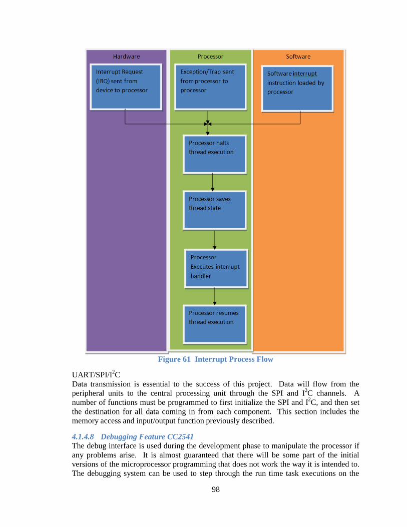
98
Figure 61 Interrupt Process Flow
UART/SPI/I2C
Data transmission is essential to the success of this project. Data will flow from the
peripheral units to the central processing unit through the SPI and I2C channels. A
number of functions must be programmed to first initialize the SPI and I2C, and then set
the destination for all data coming in from each component. This section includes the
memory access and input/output function previously described.
4.1.4.8 Debugging Feature CC2541
The debug interface is used during the development phase to manipulate the processor if
any problems arise. It is almost guaranteed that there will be some part of the initial
versions of the microprocessor programming that does not work the way it is intended to.
The debugging system can be used to step through the run time task executions on the

99
microprocessor to identify the problems. This is invaluable if a part of the program does
not work in the way it is supposed to. The debug interface uses a SPI-like two-wire
interface using the pin P2.1 for debug data and P2.2 for the debug clock. Table 23 shows
the basic AC characteristics of the debug interface.
Table 23 AC Characteristics of the debug interface
Figure 62 below illustrates the timing characteristics of the debug clock when the
RESET_N pin is pulled low. Initially, there is a short delay between the reset and the
first falling edge of the debug clock. When the reset pin is pulled high again, there is
another pause before the first rising edge of the clock.
Figure 62 Timing Characteristics of the Debug Clock. Reproduced without
alteration with permission from Texas Instruments
Figure 63 below shows the data signal characteristics of the debugging system. The
debug data is setup on the rising edge of the debug clock. The setup time of the debug
data originating from the CC2541 is shown by the term t6. The next term, t7, shows the
hold time that the data must remain at a constant level in order to be successfully read by
Parameter Test Conditions Min Typ Max Unit
fclk_dbg Debug clock frequency 12 MHz
t1 Allowed high pulse on clock 35 ns
t2 Allowed low pulse on clock 35 ns
t3 EXT_RESET_N low to first
falling edge on debug clock167 ns
t4 Debug data setup 83 ns
t5 EXT_RESET_N high to first
debug command83 ns
t6 Debug data setup 2 ns
t7 Debug data hold 4 ns
t8 Clock-to-data delay Load = 10 pF 30 ns

100
the system. The data is read on the falling edge of the debug clock. The last term, t8,
shows the delay time from the rising edge of the clock to the end of the data bit.
Figure 63 Timing Characteristics of the Data Signal of the debugging system.
Reproduced without alteration with permission by Texas Instruments
Figure 64 below illustrates a typical debug command sequence. The command byte is
read by the debug interface to configure the debugger. Data bytes are then read to the
system until the data pad direction is changed from input to output. Then data can be
transferred out from the system.
Figure 64 Typical Debug commence sequence. Reprinted without alteration with
permission from Texas Instruments
4.1.4.9 CC2541 debug device
The CC2541 requires a programming application to implement the software designed to
run the microprocessor. The CC debugger is a device that is used to run debugging
software and for flash programming. There are two PC tools that couple with the CC
debugger to run the software on the microprocessor: the SmartRF Flash Programmer
from Texas Instruments and the IAR Embedded Workbench for 8051 from IAR Systems.

101
The SmartRF Studio is the preferred PC tool in this project due to the cost of the IAR
Embedded Workbench.
The minimum connection for the connecting the CC Debugger to the System on Chip
device requires the Debug Clock signal and Debug Data signal connected from P2.1 and
P2.2, respectively, on the SoC to pin 3 and 4 on the Target Connector. Resetn must also
be connected between devices. The pin-out diagram is shown in Figure 65. To use the
full packet sniffer capabilities of the debugger, the SPI bus must also be connected to the
SoC device. The SPI bus is used to read RF packets from the SoC device. The CC2541
can also configure its RF SoC to operate as SPI slaves through one of the USART
terminals. The TI SoC devices only support two pin configurations to act in this manner:
USART0, alt1; USART1, alt2. The CC2541 supports the USART1, alt2 configuration.
Table 24 shows the pin out details of this configuration. The CC debugger will be
connected to the CC2541 in this manner and can be referenced back to the schematic
diagram in Figure 49 and 51
Figure 65 CC Debugger Target Connector Pin-Out. Reprinted without alteration
with permission from Texas Instruments
Table 24 USART Pin Out Details. Reprinted without alteration with permission
from Texas Instruments
4.1.5 User Interface Design
As the most visible aspect of the product, having an instinctive experience for the user
interface is a huge advantage. A clunky user experience can kill an application in its
infancy. In particular, in the case of a baby monitor, experience flow is paramount to the
entire operation. With important aspects such as safety, security and responsiveness, a
baby monitor requires the highest standards for human computer interaction (HCI). For
Baby Peas’ ground station unit, a number of choices exist; the three most common ones
102
are simple embedded LCD screens, desktops, and smart phones. While the first option,
embedded LCD screens, would be the cheapest selection, it also tends to be the least
attractive and least consumer friendly. Intended for a more industrial settings or niche
markets, these screens would not function well for the needs of a baby monitor. The
chance of missing critical information undermines the safety and security goals. In
addition, having a separate ground station, to the peripheral ankle mounted sensor,
generates more clutter in the unit. Parents of newborns would surely appreciate any
effort in removing clutter. Option two, desktops, has much potential and offers a greater
power in applications and calculations. In addition, most households that would purchase
the Baby Peas unit would have some version of a home pc. However, it does not matter
how powerful the unit is if the unit lacks ergonomics. Having mobility in baby monitors
trumps the desktop option, leaving smart phones as the best option, having both clarity
and mobility. Despite the obvious suitability of cell phones or tablets, LCD with resistive
touch and personal computer options are still considered for the developmental portions
of the peripheral sensors and microprocessor prototyping, and can be included in the final
product if the mobile phone or tablet does not provide the best user experience. There are
several options for touch screens.
4.1.5.1 Touchscreen
In today’s world, a common user interface for everyday consumer smart phone
applications is a touch screen due to its innately intuitive nature. The tangibility of a
touch screen creates a closer experience for the user and allows the developer to create
applications that may be complex in the backend, but have clear and concise availability
on the front end facing the consumer. This suits Baby Peas particularly well due to the
strong date driven character of the unit. All information gathered is quantifiable to both
general statistics and to the individual’s historical statistics. To have a user shift through
all that can create confusion. Having a touch screen simplifies the process, leaving the
caretaker free to make higher level decisions. As mentioned above, one route for design
is the mobile phone, the second route is an LCD touch screen attached to a base station,
and the third route is a personal computer screen. The next section goes over the finer
points of the two types of touch screens and why resistive was selected.
4.1.5.1.1 Resistive Touch
Resistive touch screens comprise of electrically conductive and resistive layers on a glass
panel. Sometimes acrylic panels are also used. Figure 66 shows a generalized picture of
the glass material and two layers that are typically manufactured with indium tin
oxide.[52]

103
Figure 66 Resistive Touch Screen, Reprinted without alteration with permission
from Texas Instruments
The base layer is called the matrix, a layer with stripped electrodes in a pattern, while the
second layer is called the analogue, a layer with transparent electrodes. As the user
draws their finger across the screen, the layers touch at the figure junction and complete
the circuit at the point, causing a differential in the system. The primarily mode of
sensing is pressure, so a resistive touch screen can be used by any object such as human
finger, pen, or pointer. The coordinates of activity is sensed using two industry standard,
the 4-wire and the 5-wire configuration. Figure 67, shows the two typical layouts.[52]
Figure 67 Resistive Touchscreen Layouts, Reprinted without alteration with
permission from Texas Instruments
Resistive screens are the cheaper of the two touch screen options and have higher
resolution, often being used in handwriting recognition capacity. In addition, as
discussed earlier, any object can be used as the pen. However, it does have some
disadvantages, including less responsive to the pressure of touch. Because the top layer

104
is being pressed down into the bottom layer, a certain pressure threshold must be met
before the circuit registers the touch. In addition the screen might not have as great of a
contrast due to internal reflections. In addition, because the top layer is flexible enough
so that it can deform to a closer position with the bottom layer, it damages more readily
than capacitive screens. Finally a resistive screen captures one touch a time and will not
support multi-touch.[49]
4.1.5.1.2 Capacitive Touch
The capacitive touch has two layers of glass, spaced out slightly, and coated with a
conductor. This basically forms parallel plate capacitor. As the user touches the screen,
the capacitance changes and the microprocessor can sense the change in the electrostatic
field. While the screens look very sharp due to the rigid nature of the two glass layers
and lack of deformation from the stylus or finger, capacitive touch screens are rather
expensive and require the user to employ finger or other conductive material to register
touches. The other upside of capacitive touch is the ability to multi-touch. However, due
to the nature of the project, developing a capacitive touch screen would be prohibitively
expensive. [50]
4.1.5.1.3 Touch Screen kits
It is recommended to buy a kit rather than develop a prototype touch screen due to cost,
time and expertise. There are several kits available in the market for purchase. For
example, 4D systems makes a resistive LCD that interfaces with a Raspberry Pi, a cheap
and light portable microcontroller. It is recommended to develop touch screens as plan b,
for it introduces more unknowns into the project and raises development costs by quite a
bit. A 3.2” screen from 4D sells for $84.95 on the well-known hobby site, Sparkfun.[51]
4.1.5.2 Software Development
Writing and optimizing code forms a significant portion of this project. An earlier
section went over the three major market share platforms for development: Android,
Windows, and iOS. The choice between the three involved several levels of calculations;
availability of open source, entry to market cost, east of development, and market share.
As a student project, gleaning information from other sources constitute a significant
portion of the journey. An open source platform usually contains a larger and more
active developer user base. In this case, of the three platforms, Android is known for
being open source and having large samples of code available for learning. While
Windows has the backing of Microsoft and large amounts of documentation, its market
share is simply too low compared to Android or iOS to seriously consider having the
Windows platform as the ground unit. The entry to market is also another serious
consideration, due to the novice nature of the group’s experience in mobile development.
In addition, the group also has limited funds and the mobile portion is just a part of the
whole project. After looking at the different price points of developer sign up fees,
Android was deemed the best due to the low onetime cost. One hurdle is the newness of
the Bluetooth Low Energy protocol. Android devices being released presently support
the Bluetooth LE, however, android devices released before, despite having the necessary
hardware, do not support Bluetooth LE.

105
4.1.5.3 Software diagrams
Software High Level System Block Diagram
*These are optional modules. If time permits, optional modules will be added to the
system.
BLE V4.0
Receiver
Communications
Framework
Applications
Framework
Notifications Utilities* User
Interface
View historical
graph
Email/text
results*
Settings and
themes*
Editor to create infant’s
profile*
Alarms
Low Battery
Sensor
overview
Sensor
selection
Decision
Algorithm
Figure 68 Software Block Diagram

106
4.1.5.4 Class diagram
Problem statement: Need to create a program to gather data, sort data and display it to
end user. The program will be used by the end user to see the status of infant’s
biomarkers of pulse, temperature, oxygen level, and orientation. The program will also
alert the user if certain conditions are not met for each sensor. Figure 69 below is the
class diagrams for the base station monitor (Smart Phone).
Figure 69 Class Diagram for Smart Phone User interface device - data collection,
parsing and humane computer interaction Class Diagram.
4.1.6 Bluetooth Handshake
As discussed in 3.2.4, after looking through the different communication protocols, it is
decided that Bluetooth would be the best fit for Baby Peas. Light on power consumption,
this protocol is well used and well documented. Additionally, the new Bluetooth Low
Power, or Bluetooth Smart, lowers the power even more.
4.1.6.1 Android Platform for Classic Bluetooth
Bluetooth network stack is already supported in the Android platform, and native
application programming interface (API) operations include other Bluetooth device scan,
query local Bluetooth adapter for paired Bluetooth devices, RFCOMM channels, service
discovery, data transference between devices and multiple connections. Basically, API is
a set of functions with an unique task. Android Bluetooth API can be broken into four
categories of setting up the Bluetooth device itself, searching for other Bluetooth devices
in the vicinity, connecting, and data transference. [56]

107
4.1.6.1.1 Setting up the Bluetooth device:
Step one is to verify Bluetooth capability and switch on the Bluetooth. The user can
manually enable Bluetooth option under system menu, but if the option is disabled, the
application can ask the user to enable the Bluetooth with the Bluetooth Adapter API
(Figure 70).
Figure 70 Bluetooth Adapter API, reprinted without alteration and with permission
courtesy of Android
The Bluetooth Adapter is the basic requirement for any Bluetooth activity. In the code,
the device is first asked to search for the device’s Bluetooth adapter by the
getDefaultAdapter() call. If the call returns null, then the adapter does not exist and no
Bluetooth connection can be made. If an adapter exists, the code can use isEnabled() to
look at the status of the adapter. If the user has manually enabled the Bluetooth module,
then the result would indicate false. If the user has not manually enabled the Bluetooth
module, then the code can enable the Bluetooth by startActivityForResult() function call
and ACTION_REQUEST_ENABLE Intent. This displays Figure 70 screen to the user.
When the user clicks yes, then the Bluetooth device is enabled and can start searching for
other devices in the vicinity.[56]
4.1.6.1.2 Searching for other devices:
The two options for this portion is device discovery or looking for list of paired devices.
Either method should work for Baby Peas. For device discover, a general call is made
out to any discoverable devices in range, and once an object is discovered, a connection
is made by exchanging identifying information. For list of paired devices, identifying
information is already stored on the home Bluetooth device, and the benefit of that is the
connection can be made whenever the range is optimal. Due to the time saving nature of

108
paired devices, it is probably the best method for Baby Peas. To have a unique monitor
for each baby furthers the cause of individualized units.
The first step to query is to use the getBondedDevices() call. This allows the home
device to look for unique media access control address (MAC address) that is stored in
the hardware of the network interface controller. In addition to the phone doing the
querying, the satellite device, the peripheral ankle sensor unit, can also query for the
phone. In that case, the phone will have to enable discoverability. Using the
startActivityForResult(Intent, int) and ACTION_REQUEST_DISCOVERABLE, the
phone is able to be discovered by the sock unit. This is a decision for the designer, due to
power and timing considerations. Figure 71 below is an example of what alert might
look like on the smart phone devices once the peripheral ankle sensor unit queries for
other devices and the smart phone picks up that query.[56]
Figure 71 Possible alert form and smart phone device, reprinted without alteration
courtesy of Android
4.1.6.1.3 Connecting device as server-side:
This step is critically important to the communications portion of the unit; server-side and
client-side operations must take place on the same RFCOMM channel. Server-side
portion opens with BluetoothServerSocket API, and listens to requests for connection.
Once server-side accepts the connection, the BluetoothSocket is connected and the
server-side can stop BluetoothServerSocket (so additional requests will not be honored).
Some commands used are listenUsingRFcommWithServiceRecord(String, UUID),
accept(), and close(). For the first one, the string is the name of the service. The accept
command will initiate connected BluetoothSocket only if the query was accepted.
Finally the close() call sets down the query and no additional connections will be made.
In the case of multiple satellite units, the close() call can be adjusted so that more
connections can be made. To the right is a sample connection code from android
developer site.Connecting device as client-side:

109
The ground station must first get BluetoothDevice that represents the satellite device.
Several commands used are creatRfcommSocketToServiceRecord(UUID),
listenUsingRfcommWithServiceRecord(String, UUID), and connect(). Figure 72 below is
sample code for Android applications on how the Bluetooth connection could be made.
The Baby Peas project could use this as a platform in helping the development of the
smart phone application.[56]
Figure 72 Example code for Android Bluetooth Connections, reprinted without
alteration and with permission from Android

110
4.1.6.1.4 Managing a connection:
Once connection is made, the devices exchange data via InputStream, OutputStream,
read(byte[]), and write (byte[]) calls.
4.1.6.1.5 Profiles:
Android offers several Bluetooth profiles: Headset, A2DP, and Health Device. Headset
is a profile for using wireless headsets via interprocess communication, a method for
exchanging data through many threads. A2DP stands for Advanced Audio Distribution
Profile and it controls the audio quality coming in from the wireless device. The project
is concerned primarily with the Health Device profile. With this profile, the Android
device can exchange information with health monitors such as pulse, temperature,
weight, and blood monitors. [56]
APIs for the health profile include BluetoothHealth, BluetoothHealthCallback, and
BluetoothHealthConfiguration. The arrangement of the two devices is of source and
sink; the source is the measuring device and the sink is the home station that is receiving
the data. [56]
5 Project Prototype Construction and Coding
5.1 Parts Acquisition and BOM
5.1.1 Part Vendors
To ensure uninterrupted progress in the project, we have to find reliable part and
components providers. Newark, Digikey, and Sparkfun are the main distributors along
with local hobby stores like Skycraft Part and Supply.
5.1.2 Newark
Newark Corporation (Newark element 14) is an electronic component distributer based in
Chicago, Illinois. Founded in 1934, Newark Electric was a small shop mainly selling
radio parts. It is one of the major distributors of electronic components and testing
hardware today. One of the advantages of using Newark is its affiliation with Cadsoft
Eagle schematic capture software. Cadsoft Eagle has an option provided by Newark
which allows the designer, once the schematic is complete, to assign specific
manufacturing part numbers from its database to easily create a bill of material. This
feature alone could save hours in looking up each individual component on the 3 different
websites and then comparing costs. Newark provides both the manufacturing part
number and the Newark assigned part number. This way if Newark does not stock the
item it allows the designer to look elsewhere for a possible part solution.
5.1.2.1 Digikey
Digikey was founded in 1972 providing wide selections of electrical components. It is
now serving North America, Europe, and Asia. Its headquarters is based in Thief River
Falls, Minnesota, USA. With 99.95% orders shipped on the same day, it could be a very
reliable source for Baby Peas project.

111
5.1.2.2 Sparkfun and local hobby centers
Sparkfun is an online retail store which offers parts for electronic projects. Sparkfun also
offers classes and online tutorials through its department of education, a valuable
resource for hobbyists and developers.
5.1.2.3 Price list of Hardware “BOM” / Development Tools
Based on our research, most suppliers have plenty of quantity in stock or offer
alternatives. Newark offers the lowest prices. Some parts are available as free samples
from the manufactures. Parts needed for the fabrication of the PCB are listed Bill of
materials Table 25. Not all components are listed which are needed for the PCB but the
high level sensor parts which are the most expensive are listed. Table 26 is a list of
Development Kits the Baby Peas project will need for product realization.
Table 25 Introductory BOM for the Peripheral sensor PCB
Table 26 Software Development Kit BOM
Part Quantity Price Vendor SampleTI AFE4490 1 $18.67 Digikey Yes, from TI
$10.72 Digikey
$12.95 Sparkfun
$1.46 Digikey
$1.01 Newark
MTE5066C-UR 1 $2.73 Digikey N/A
Fairchild QEB363 1 $0.46 Mouser N/A
Fairchild QSB34CGR 1 $0.84 Mouser N/A
Advance Photonix
PDI-E839
$6.62 Digikey
$5.75 Newark
$2.31 Digikey
$1.82 Newark
PST-LC24* 1 $15.00 Powerstream N/A
Lir2477* 1 $5.00 Powerstream N/A
PCB board 1 $33.00 4PCB N/A
Crystal 32.786 KHz 1 $0.24 Digikey N/A
Crystal 8MHz 1 $0.20 Digikey N/A
Crystal 4MHz 1 $0.21 Digikey N/A
Capacitor 0.01uF 1 $0.10 Digikey N/A
Capacitor 0.1uF 1 $0.10 Digikey N/A
Resistor 1M Ohm 1 $0.10 Digikey N/A
Resistor 0 Ohm 1 $0.10 Digikey N/A
Inductor 2.2uH 1 $0.14 Digikey N/A
Yes, from TI
Invensense MPU-60x0 series 1 N/A
TI TMP006 1 $3.89 Digikey
TI TMP103 1 Yes, from TI
1 $5.95 Octopart N/A
TI CC2541 1 Yes, from TI
TPS62730* 1 Yes, from TI
Part Quantity Price Vendor SampleSK-24PTU-PI* 1 74.4 Mouser N/A
CC2541 SensorTag Development Kit 1 33 TI Yes, from TI
CC2541 SensorTag Development Kit 1 99 TI Yes, from TI
CC2541 Evaluation Model Kit 1 99 TI Yes, from TI

112
5.2 PCB Vendor and Assembly
Printed Circuit Board Vendors provide services which take something called gerber files
which are generated from a type of CAD software tool (like CAD EagleSoft) and are able
to generate a fabricated Printed Circuit Board without any components soldered to the
board. Printed Circuit Board assembly houses provide services which place each
component on the circuit board and then solder them. They use pick and place machines
which automatically place each part in the right location and position on the PCB and
then run the board through an oven at a specified temperature per part which enables the
part to be properly soldered down. They then run the board through a machine which
automatically provides visual inspection of the solder connections. They have certified
inspectors which provide visual inspection of the boards as well.
5.2.1 PCB Vendors
Printed Circuit Board (PCB) fabrication has a wide selection of possibilities to choose
from. Due to time constraints a vendor which offers low pricing and quick turnaround
time will be used for the PCB fabrication of the peripheral device PCB.
5.2.1.1 4PCB
4PCB is an online manufacturing provider of Printed Circuit Boards. They provide 2
layer boards (student pricing) covering 60 square inches of circuit board space for $33.00
dollars or a 4 layer board covering 30 square inches of circuit board space for $66.00
dollars. They have a turnaround time of 5 days and also provide free Design for
manufacturing tests which means they look at the PCB layout provided and check to
make sure tolerances between trace widths and such are within the standards for PCB
fabrication.
5.2.1.2 PCB Fabexpress
PCB Fabexpress is another online PCB vendor which provides quick turnaround times of
5 days but have some minimum order requirements which drive up the price. Any 2
layer bare bones PCB (no silk screen or solder mask) has a standard cost of $40.00 with
$.60 added for every square inch. While customization for size and cost is a great option
the minimum order quantity could get expensive if a redesign effort needs to be done
during the project testing and evaluation period.
5.2.1.3 Custom Circuit Boards
Custom Circuit Boards provides PCB fabrication with extremely fast turnaround time of
24 hours if needed. They do not have a standard 2 or 4 layer pricing matrix but quote
each PCB separately. When the PCB design is completed for the Baby Peas project the
gerber files will be submitted for quote to obtain pricing.
From the evaluation of these three companies it is decided the Baby Peas’ PCB
fabrication will be done by 4 PCB. The pricing and space could not be matched along
with the added feature of the design for manufacturability allows an expert pair of eyes to
evaluate the PCB for any mistakes which could hinder the assembly of parts onto the
board. Custom Circuit Boards will be approached once the PCB layout design is
completed to receive a price quote. Once completed it will be a backup plan in case
schedules start to become a problem and a PCB is needed quickly.

113
5.2.2 PCB Assembly Houses
For the PCB assembly, the Baby pea’s project wanted to approach local PCB assembly
houses which provide component assembly to PCB services. Two local companies were
researched as possible candidates for assembly of the PCB due to the small nature of
QFN package devices. Pricing and turnaround times will be the driving factor in
choosing an assembly service.
5.2.2.1 QMS (Quality Manufacturing Solutions)
Quality Manufacturing Solutions is a local PCB assembly house located in the Lake
Mary, Fl area which not only provides PCB assembly services but a host of engineering,
manufacturing, test, configuration control, quality and supply chain management services
to their customers. They specialize in rapid prototype to medium volume production.
They have the ability to perform BGA rework and X-ray services if needed. Judy Kelch
is a project manager at QMS and will be approached for sponsorship options with the
Baby Peas’ project which could involve financial contributions or design advice for PCB
layout and inspection services of the solder connections. Pricing for QMS to perform a
pick and place operation and run the boards through their ovens would be beyond the
affordability of the project if the group had to pay for it.
5.2.2.2 Conilec
Conilec is a local PCB assembly house located in Deland, FL. They too provide a wealth
of services to their customers. They assign specific program managers to all their
customers and are the point of contact for any interactions between the two parties.
Conilec will be approached for sponsorship options as well. A price quote could not be
obtained without a finished PCB layout design.
5.2.2.3 DIY (Do it yourself)
The baby pea’s project has a certified J-STD-001 surface mount solder technician which
is able to solder down to 0201 size packages along with LGA and QFN packages. The
group has obtained a hot air pencil soldering system along with soldering iron equipment
for surface mount PCB assembly and a microscope for inspection of solder connections.
The group has the ability to solder all components onto the PCB and rework each
component of the PCB as needed.
The DIY approach seems to be the best option since the only cost incurred will be solder
materials and time, but it allows for flexibility in the schedule because the assembly and
rework are not relied upon by people outside of the group. The hot air pencil will be used
for difficult components like the QFN and BGA packages. The soldering iron will be
used for all other leaded surface mount components. In addition, the do it yourself
approach will give invaluable experience to the inexperienced group members.

114
6 Project Prototype Testing
6.1 Hardware Prototype Testing
Hardware testing needs to be thorough, methodical, and controlled for the Baby peas’
project to be successful. Hardware testing can make or break a project. There is a fine
line between how much a company should spend on testing hardware and software before
releasing products to market. Testing costs companies money and for every day the
product is not on the shelves is more money the company is losing. However, projects
also realize not enough testing can lead to product failure in the field which can be
detrimental in the long run for the survival of the company. The Baby pea’s project is
opting for an abundance of test scenarios because of the nature of the product. Since
safety is of the utmost concern, any failure on the device which could cause even the
slightest amount of harm to the individual is unacceptable. The project specifications
must be met and back up protection code and hardware must be put in place to allow for
as many possible scenarios which could cause harm to the user are explored. In addition,
testing parameters must be calibrated with the baseline set for infants and not adults. In
the following sections a comprehensive hardware and software test matrix will be
provided as to cover each sub system and full system test parameters which have to meet
a certain criteria before the product could be labeled as a success. To such an end, the
Baby pea’s project will take time to layout the PCB in a specific way which allows each
sub system to be connected and disconnected from the CC2541 and power supply
circuitry through the use of series 0 ohm resistors. This way each sub system can be
connected and tested separately from all other interactions with other subsystems. This
will allow individual sub systems to be brought up to specifications and debugged easily.
Any dysfunction can be located in a timely manner and either switched out or replaced
with another component. After all subsystem categories completed testing, one
subsystem at a time will be added in and retested for compatibility. The test equipment
used for evaluating the hardware will be oscilloscopes, function generators, digital
multimeters, power supplies, spectrum analyzers, and logic analyzers. All the testing will
be done with electrostatic protection in mind.
6.1.1 Battery, Regulator, and Charging Circuits
The first circuit to be tested is the battery, regulator, and charging circuit. To test this
circuit, the TPS62740 will be soldered onto the PCB first with supporting circuitry
(CC2541 will also be soldered to the PCB). On the switched output of the regulator there
will be a 0 ohm series resistor which will not be placed. This will allow isolation to the
rest of the PCB and an external dummy load resistor can be soldering in via a white wire.
Another white wire can be connected to the battery terminals, allowing for an external
power supply to be connected in. Table 27 walks through the necessary tests which will
be performed.

115
Table 27 Battery, Regulator, and Charging circuit Test Matrix
6.1.1.1 Temperature Sensor Hardware
The temperature sensor will be the next system to be tested on the PCB. For all the
peripherals, the CC2541 software code will have to be completed and debugged at the
same time as the peripherals are being added. Once this is completed the data
communication (I2C) can be probed and evaluated using an O-scope to check the SDA,
SCL, and Chip select lines are operating properly. For the hardware test the output of the
data from the TMP006 is inconsequential. Hardware testing is making sure the device
operates under the specifications in the data sheet. Table 28 below transitions
Table 28 TMP temperature Hardware Test Matrix
TEST Procedure Description Expected Result
1 In/Out Resistance Checks With DMM Measure Vin and
Vout pins on TPS62740
Test validates input and output
are not connected to ground and
Vin and Vout soldered properly
Vin = High impedance
Vout = High Impedance
2 Input Voltage Measurement Connect external DC power
supply to Battery Terminals,
V = 3.6v , I limit = 110mA
Validates input battery terminals
are properly designed for Input
Voltage
Vin = 3.6V
3 Switched Vout
measurement
Same Vin setup, High set on
pin 12 (EN), O-scope on
Switched line Test Point
Checking the 3.3v rail to validate
output switched signal
Vout = 3.3v
Vripple < 20mVpp
4 Switched Vout response to
High and Low impedance
loads
external High ohm and low ohm
dummy loads switched by
external fet controlled by
function generator
Validates output stability of the
TPS62740 to the varying load
resistances experianced during
full operation.
Output Voltage remains
stable with no ringing on
the output after High/Low
switch
5 Battery Function Test Remove External Power
Supply and insert Coin Cell
Battery into Battery holder clip
and Retest parts 1-4.
Validates the Battery can operate
the voltage regulator
Same as expected results
from parts 1-4
6 Battery Charging Circuit Plug in external battery charging
circuit and verify battery is
charging via digital multimeter
This validates the TPS62740 is in
shut down mode during charging
operations and the battery is
charging properly
Vin on the TPS62740 = 0v
and proper battery
charging operation is
observed.
Test Procedure Description Expected Result
1 Proper Solder
connections
Measure the input resistance on
Vin pin to ground with a DMM
This verifies the component Voltage
input is not shorted and should operate
properly when powered
High impedance
2 Chip Select Line Measure the chip select line with
an O-scope to verify proper high
low transitions
This verifies the ouput from the CC2541
is controlling the chip select line
High / low transitions
from 0v to VDD
(square wave)
3 SDA / SCL line test
(chip select line active
high)
Measure the chip select line,
SDA, and SCL lines with an O-
scope to verify clock frequency
(SCL) and verify SDA (Data)
Verifies accuracy and operation of the
clock frequency from the CC2541 on
the SCL line and verifies SDA high/low
transitions the data is being ouput from
the TMP006
SCL should measure
the clock frequency
output from CC2541 /
SDA should be a
sqaure wave
4 SDA / SCL line test
(chip select line active
low)
Measure the chip select line,
SDA, and SCL lines with an O-
scope.
Verifies when chip select line is active
low the TMP006 should be off and
SDA output data should be either
always high or always low.
chip select line to be
low. SDA line to be
constant high or
constant low.

116
6.1.1.2 Body Position Sensor Hardware
Once the TMP006 hardware device is tested the next device to be placed into circuit will
be the MPU-6000 body position sensor. First the TMP006 will be disconnected from the
circuit. The MPU-6000 will then be installed and tested in the same manner as the
TMP006. Since both devices interact with the CC2541 over I2C, the device testing
characteristics will be the same as shown in Table 28 with the difference being the device
name.
6.1.1.3 Pulse Oximetry Sensor Hardware
The pulse oximetry sensor hardware circuit is tested next. The temperature sensor
TMP006 and the MPU-6000 can remain in circuit except for their input voltage. Their
data lines interact with the CC2541 over I2C whereas the AFE4490 uses a SPI bus to
transmit data to the microcontroller. Testing is similar to the two previous sensors but the
outputs which drive the LED’s will be measured along with the SPI bus data line outputs.
Since an 8Mhz external crystal oscillator will also be in the circuit we are going to
measure the stability of the oscillator. Table 29 displays the test matrix for the Pulse
Oxemetry AFE4490 hardware circuit.
Table 29 Test Matrix for AFE4490 Pulse Oximetry Sensor
Test Procedure Description Expected Result
1 Proper Solder Connections Measure input resistance on Vin to
ground with a DMM
Verifies the input voltage line to the
AFE4490 is not shorted to ground
High impedance
2 External 8 MHz crystal
oscillator measurement
Use an O-scope to measure 8MHz
crystal oscillator
Verifies a proper 8 MHz stable
oscillator frequency is present
O-scope will read 8MHz
signal with 3.3vpp
applitude
3 LED 1 and LED 2 On/Off Visually check to make sure 660 nm
LED turns On/Off, Make sure 940nm
LED turns on and off
Both the 660nm and 940nm
LED's should turn on and off
repeately while the s/w is running
from the CC2541
LED 660nm is on then off
LED 940nm is on then off
per specified times in
CC2541 code.
4 Photo Diode Check Measure in line current to using a
DMM to verify current pulses are
present
Measuring the in line current will
display the Photo Diode is picking
up the light from the LED when
they are on
Durring LED's on the
Photo Diode Currents
should be increasing while
when the LED's are off
the current should be
decreasing.
5 SPI Bus Measurements Using an O-scope. Measure SPISTE
Pin 26 on the AFE4490
Verify High and Low pulses are
seen on the O-scope verifying
proper communication between
AFE4490 and CC2541
high and low pulses from
0v to VDD should be
displayed on the O-scope
6 SPI Bus Measurements Using an O-scope. Measure SPISTE
Pin 26 on the AFE4491
Verify High and Low pulses are
seen on the O-scope verifying
proper communication between
AFE4490 and CC2542
high and low pulses from
0v to VDD should be
displayed on the O-scope
7 SPI Data Measurements Using an O-scope check SPISTE,
SCLK, SPSIMO, and SPSOMI
Verify during active mode on
SPISTE that SCLK , SPISIMO
and SPISOMI lines are
transitioning High/Low
High/Low transisitions are
seen on SPISOMI,
SPISOMI lines. SCLK
frequency is accurate per
settings in CC2541
8 SPI Data Measurements
during inactive mode
Using an O-scope check SPISTE,
SCLK, SPSIMO, and SPSOMI
Verify during inactive mode on
SPISTE that SCLK , SPISIMO
and SPISOMI lines are tansmitting
constant high or constant low
During inactive modes
there should be no data
transmissions over the SPI
bus.

117
6.1.2 Wireless Communications Hardware Test
Due to the nature of the wireless communications hardware being a System on Chip
CC2541 most of the testing on the input circuitry was taken care of during previous
testing of the sensors. Things which can be tested are the output RF power from the
system to verify proper gain flatness is maintained over the entire transmit frequency
band. Software settings within the CC2541 can program the different transmit output
power settings. Tests will be conducted which check the Max, Mid, and Min output
power settings. Also two external crystal oscillators are being used which need to be
verified as operational. Table 30 below displays the test matrix for the CC2541 circuitry
portion.
Table 30 Test Matrix for CC2541 Wireless Communications Hardware
Test Procedure Description Expected Result
1 Output Power Test
RF_N pin (Max Power)
Using a Spectrum Analyzer
and RF probe check RF_N
pin during transmit. (TXPower
Mode set to 0xE1)
This test will look at the gain
flatness over the operating
frequency band to verify the
CC2541 is properly transmitting
Gain flatness should be +/- 1dB
over frequency band with an
output power of 0dB
2 Output Power Test
RF_P pin (Max Power)
Using a Spectrum Analyzer
and RF probe check RF_N
pin during transmit(TXPower
Mode set to 0XE1)
This test will look at the gain
flatness over the operating
frequency band to verify the
CC2541 is properly transmitting
Gain flatness should be +/- 1dB
over frequency band with an
output power of 0dB
3 Output Power Test
RF_N pin (Mid Power)
Using a Spectrum Analyzer
and RF probe check RF_N
pin during transmit. (TXPower
Mode set to 0x91)
This test will look at the gain
flatness over the operating
frequency band to verify the
CC2541 is properly transmitting
Gain flatness should be +/- 1dB
over frequency band with an
output power of -10dB
4 Output Power Test
RF_P pin (Mid Power)
Using a Spectrum Analyzer
and RF probe check RF_N
pin during transmit(TXPower
Mode set to 0X91)
This test will look at the gain
flatness over the operating
frequency band to verify the
CC2541 is properly transmitting
Gain flatness should be +/- 1dB
over frequency band with an
output power of -10dB
5 Output Power Test
RF_N pin (Low Power)
Using a Spectrum Analyzer
and RF probe check RF_N
pin during transmit. (TXPower
Mode set to 0x41)
This test will look at the gain
flatness over the operating
frequency band to verify the
CC2541 is properly transmitting
Gain flatness should be +/- 1dB
over frequency band with an
output power of -20dB
6 Output Power Test
RF_P pin (Low Power)
Using a Spectrum Analyzer
and RF probe check RF_N
pin during transmit(TXPower
Mode set to 0X41)
This test will look at the gain
flatness over the operating
frequency band to verify the
CC2541 is properly transmitting
Gain flatness should be +/- 1dB
over frequency band with an
output power of -20dB
7 32MHz crystal oscillator
Test
Use an O-scope to measure
32MHz crystal oscillator
Verifies a proper 32 MHz stable
oscillator frequency is present
O-scope will read 32MHz
signal with 3.3vpp applitude
8 32.768 kHz crystal
oscillator Test
Use an O-scope to measure
32.768 kHz crystal oscillator
Verifies a proper 32.768 kHz
stable oscillator frequency is
present
O-scope will read 32.768 kHz
signal with 3.3vpp applitude

118
Once the completion of the CC2541 device has been tested, all devices will be inserted
back into the circuit and will be ready for system level testing.
6.2 Software Prototype Testing
The Software testing consists of the CC2541 embedded coding and the user interface
display device for Android compatible Bluetooth smart devices. Software “glitches” and
non-intuitive user interface applications can cause the reliability of the product to be
called into question from the user. The following table documents the possible route of
testing for the software usability. In addition to the table, the unit should be operated by
those who are unfamiliar to the project. This ensures that the design of the app is
intuitive enough for the lay users.
6.2.1 CC2541 Software Testing
Software loaded onto the CC2541 is imperative for the hardware sensors of the system to
work properly. The testing of the code will consist of a parallel path along with the
hardware section during hardware prototype testing. Since the embedded code will be
split up into separate function operations for talking to and sorting data from each sensor
at different times the software code can be commented or uncommented depending on
which functions are needed for each specific sensor device. Table 31 is a walkthrough of
the individual tests which will be run to verify the software code loaded on the CC2541 is
functioning properly.

119
Table 31 Test Matrix for Software functions of the CC2541 microcontroller
6.2.2 User Interface Module Software Test
The user interface hardware to be used for the baby peas’ project will be either a
Samsung Galaxy S3/4 phone or some other Bluetooth low energy compatible device with
a display. The main reason to test an applications user interactive software is this is what
the customer sees all of the time. If this portion of the device is not quick, easy, robust,
and intuitive then the user will have no desire to use the device regardless of how good
the hardware accuracy is. The Software will be tested by loading the designed
application on the smart device and walking through each feature and validating features
load quickly and display in a way which provides all the necessary data features. For the
user interface module testing, the data being displayed does not need to be accurate. This
will be covered in the final system testing. Table 32 is a breakdown of the necessary tests
which will be accomplished to validate the user interface module software testing.
Test Procedure Description Expected Result
1 CC2541 hardware init() is
compiled and properly loaded
onto CC2541
Use IAR embedded
workbench to compile code
and load onto CC2541
Verifies the ability to
compile and load code
onto the CC2541
Code compiles with no
errors compiled code
loads successfully onto
CC2541
2 Function for enabling
TPS62740
Compile TPS62740 function
interactions and verify
TPS62740 is operating per
Test Matrix Table X
Verifies the enable and
soft start of the
TPS62740 voltage
regulator for proper
operation
No errors in compiled
code. TPS62740
operating correctly
3 Function for enabling TMP006 Compile TMP006 function
interactions and verify
TMP006 is operating per
Test Matrix Table X
Verifies the enable and
soft start of the TMP006
voltage regulator for
proper operation
No errors in compiled
code. TMP006
operating correctly
4 Function for enabling MPU-
6000
Compile MPU-6000
function interactions and
verify TPS62740 is
operating per Test Matrix
Table X
Verifies the enable and
soft start of the MPU-
6000 voltage regulator for
proper operation
No errors in compiled
code. MPU-6000
operating correctly
5 Function for enabling AFE4490 Compile AFE4490 function
interactions and verify
AFE4490 is operating per
Test Matrix Table X
Verifies the enable and
soft start of the AFE4490
voltage regulator for
proper operation
No errors in compiled
code. AFE4490
operating correctly
6 Function for enabling wireless
communications portion of the
CC2541
Compile CC2541 wireless
communications settings
Verifies the proper setup
of the wireless
communications settings
No errors in compiled
code. Bluetooth
operating correctly

120
Table 32 User Interface Software Test Matrix
6.3 System Level Testing
System level testing can be completed once all the individual subassemblies are proven to
be operating properly. System level testing verifies our project meets all the design
parameter specifications and goals required to be a successful product. System level
testing also needs to be tested in a variety of scenarios to allow for proper testing of the
different situations which may occur during the night if the product were to be placed on
a sleeping child. While child testing will not be taken, the peripheral device will be worn
by the project members and monitored throughout sleeping to validate some of the tests.
Most of the tests can be accomplished in a lab environment. Environmental temperature
testing will occur at L-3communication/Cyterra division in South Orlando. They have
graciously allowed the baby peas’ project to utilize their temperature test chambers for
environmental test validation.
6.3.1 Skin Temperature Final Test
Skin temperature final testing will be accomplished by connected the peripheral sensor
onto a group member’s ankle, turning the device on, opening up the application and
choosing the “monitor my child” option. This is the main monitoring display and will
display all 4 sensor data. The development kit “Sensor Tag” device will also be mounted
to the user very close to the project peripheral device. The Sensor Tag development kit
utilizes the same sensor device in the Baby pea’s project. The sensor tag will be
Test Procedure Description Expected Result
1 Software (SW)
application build
Compile SW code in
Software Development Kit
for Android program
Verifies properly
compiled software code
Compiled code has no
erros.
2 Software application
load onto smart
device
Connect USB cable from
laptop to smart device and
upload application software
build
Verifies proper loading
of the SW application
onto the smart device
Application load onto
smart devices is successful
3 Application Login Open the Application on the
Smart Device and provide a
Login
This verifies the
application will open on
the smart device and
start to run
Application opens and
asks the user for a login.
Login is entered and the
application moves to user
interface window
4 User Interface
Window
Walkthrough all available
options and verify each
option opens into its
respective function when
chosen
This verifies all functions
within the user window
opens and displays the
proper information
All options available open
quickly and start to
display the necessary
information requested.
5 Sensor Information
Window
In the user interface window
choose "Monitor my child".
Main data display
window which shows all
4 sensors being
monitored and their
respective information
Heart Rate, Oxygen level,
Body Position, and
Temperature are all
displayed in the diplay
device window.
6 Shutdown A stop operation is made by
the user and "Shutdown"
device is chosen
Verifies the application
can be disabled and
closed out
Application closes

121
wirelessly connected to a laptop where a user interface GUI will be running displaying
the sensor tag’s skin temperature readings. The sensor tag is a known good device and
we can use it to compare the data displayed from the sensor tag to the data being
displayed from the baby pea’s peripheral device. Table 33 is the test matrix to verify the
Skin temperature sensor meets project specifications
Table 33 Skin Temperature Final Acceptance Test matrix
6.3.2 Body position Final Test
The body position final acceptance testing will be performed in a lab environment with
no need to be attached to a user. The peripheral sensor will lay on a flat surface and be
orientated in different angles to observe accuracy of position along with alarms on the
user interface device when moved into different positions. Also being tested is a settling
time check. This test allows the user to receive a notification symbol “MOV” stating the
infant is moving and cannot obtain a steady reading for body position. Simulations of
this will entail placing the sensor on a table top in a stable position for 1 minute then
moving it rapidly for 20 seconds then setting it down again in a different position and
verifying the “MOV” icon under the body position data display portion is active during
movement and inactive during no movement. Table 34 is a the test matrix for the final
acceptance testing of the body position sensor
Test Procedure Description Expected Result
1 Skin Temperature of User
in Ambient Room Temp
Attach peripheral and
sensor tag to user ankle and
power on both assemblies
Verifies the proper
reading of the skin
temperature
Baby peas' peripheral and
sensor tag sensors are within
5% of each other
2 Skin Temperature of User
in Ambient Room
compared to thermometer
data taken orally
Attach peripheral and oral
thermometer to user and
compare temperature
results
Comparison test between
oral temperature and skin
temperature
Baby peas's peripheral
should read within +/-10% of
oral temperature.
3 Increasing temperature Place peripheral sensor on
table top and utilize a heat
gun to heat the sensor
Verifies the sensor will be
updating the user display
with increasing
temperature readings
User display should show
rising temperatures
4 Decreasing temperature Place peripheral sensor on
table top and spray the
sensor with a freeze spray
Verfies the sensor will be
updating the user display
with increasing
temperature readings
User display should show
decreasing temperature.
5 User Interface Alarms Place peripheral sensor in
environmental chamber and
set chamber to 25 degrees
C. Once stable set
temperature to 30 degrees
C. Repeat at 25 degrees C.
Verifies as a temperature
changes by 5 degrees it
causes an alarm on the
user interface display
device (adroid phone)
Alarm sounds if :
Temp ∆ +/-5 degrees from
baselined temperature
readings Baseline Temp 25c
Alarm sounds @ 30c and
20c

122
Table 34 Body Position Final Acceptance Test matrix
6.3.3 Pulse Oximetry Final Test
The pulse oximetry test is the heart and soul of the baby peas’ project. It provides heart
rate and blood oxygen levels which are critical to the data needed to see if the body is
starting to dive into a fatal state. Pulse oximetry testing will be conducted at a medical
facility which a group member is employed at. The facility has graciously allowed the
baby peas project the use of a pulse oximetry sensor to compare our sensor readings.
Table 35 is the test matrix for the pulse oximetry sensor. The sensor will be attached to
each member of the Baby pea’s project for validation over a different range of users.
Test Procedure Description Expected Result
1 Stable up Postion Place peripheral device
on a flat surface facing
up and power sensor
on
Verifies with the sensor a
flat position the reletavive
reading on the display
should be up.
User interface display
window displays "up"
position being read
2 Stable Left/Right
Side Position
Place peripheral on one
side first and then other
side next
Verifies sensor updates
position setting and gives
alarm
User interface displays
new position of "right
side" or "left side" and
gives audible alarm to
the user.
3 Stable down
Position
Place peripheral device
on a flat surface facing
down
Verifies sensor updates
position settling and gives
alarm
User interface displays
new poistion of
"down" and alerts the
user audibly
4 Settling Time Place peripheral device
on flat suface facing up,
obtain stable reading.
Shake sensor for 20
seconds then set back
down
Verifies sensor can
display movement and
recover with stable
readings
During movement, user
display should indicate
"MOV" and once
sensor settles proper
position reading should
be displayed within 5
sec

123
Table 35 Pulse Oximetry Final Test Matrix
6.3.4 Weight, Battery Life, and Wireless Range Final Test
The weight test can be conducted in a lab environment using a calibrated scale. The
Battery life will be tested overnight at each group member’s house. The wireless range
test will be conducted on UCF campus and in group member’s houses. Table 36 is the
test matrix for the remaining system parameter test specifications.
Table 36 Weight, Battery life, and Wireless Range Final Test matrix
Test Procedure Description Expected Result
1 Heart Rate Accuracy
Test (stable)
Attach peripheral to
ankle of users. Attach
medical facility Pulse
Oximetry Sensor
equipment to index
finger of user
Verifies the Pulse
Oximetry sensor and
obtain accurate heart
rate information
User displays heart
rate information and
accuracy is within
20% of the medical
facilities output
results
2 Blood Oxygen
Accuracy Test (stable)
Attach peripheral to
ankle of users. Attach
medical facility Pulse
Oximetry Sensor
equipment to index
finger of user
Verifies the Pulse
Oximetry sensor can
obtain accurate
blood oxygen levels
from a user
User display shows
blood oxygen
information and
accuracy is within
20% of the medical
facilities output
results
3 Sensor movement and
recovery
Attach peripheral to
ankle of users. Attach
medical facility Pulse
Oximetry Sensor
equipment to index
finger of user
Verifies sensor can
still obtain an
accurate reading
while sensor is still
moving
User displays
accurate heart rate
and oxygen levels
during slight
movements
Test Procedure Description Expected Result
1 Weight Test Place baby peas'
peripheral sensor on
calibrated scale
Verifies weight of
device is less than 1lbs
Device weighs < 1lb
2 Battery Life Power on baby peas'
peripheral sensor and let
sensor run until battery
dies or 12 hours is
reached
verifies the sustained
operation of the device
for 12 hours
Device runs for > 12
hours
3 Wireless Range
Outdoors
Turn on the baby peas'
peripheral sensor and
establish bluetooth
connection to user
display device (Android
Phone). Move display
device 100 feet away
from the sensor.
Verifies the wireless
range specification is
met
Device continues to
monitor all sensors and
transmits the data to the
display device at a range
of 100 feet in 12 different
radial points.

124
7 Administrative Content
The administrative content of the Baby Peas project group consists of project schedules,
milestones charts, and group roles and responsibilities. It is of the highest importance the
administrative duties to not be let go by the way side but are adhered to strictly.
7.1 Milestones and Schedule Discussion
The baby peas project is under and extremely tight schedule due to the nature of trying to
come up to speed on android application development, Bluetooth low energy
development, PCB circuit design and component interactions. It is the intent of the group
to have weekly and sometimes bi-weekly meetings to discuss actions of the week and to
monitor the progress of the schedule milestones. Table 37 and 38 below are the
Hardware and Software milestones chart, respectively, and weekly schedules for Senior
Design 1 Fall 2013.
Table 37 Hardware Tasks Milestones Chart Senior Design 1

125
The hardware portion schedule is primary driven by research on three sections – sensor
components, central processing unit, and power unit. The sensor component and the
microcontroller that controls them should be researched and procured in conjunction with
each other, as both will have to mesh for the entire unit to work. Power source research
must wait until the parameters for each sensor, the central processing unit and wireless
protocol are determined. In addition to the component selection, the hardware schedule
also includes the documentation required at the end of senior design 1. This massive
document will require a lion’s share of work and work needs to start on that as soon as
possible.
Table 38 Software Tasks Milestones Chart Senior Design 1
In addition to the hardware schedule, the software schedule for senior design 1 is a rough
guideline for the development life of this product. Like the hardware schedule, the
software also starts by researching through similar projects. This is to gain both an
understanding of the available resources and also help formulate the framework for this
project. In addition to software research, the group needs to learn some sort of object
oriented language, as most of the mobile platforms operate on object orient languages
such as Java or C#. As the group is composed of electrical engineering students who
have a foundation in C and little to no experience in object oriented programming, this is
a critical step in the developmental cycle. In addition, while the prototype will not be
built until second semester of senior design, it is feasible to look for development kits to

126
test out the software portion. Usually companies such as Texas Instruments or Freescale
will have developmental kits for developers and hobbyists to write applications for.
Below are tables 39 and 40 for the milestone charts and weekly schedules for Senior
Design 2 Spring 2014.
Table 39 Hardware Tasks Milestones Chart Senior Design 2
Hardware Tasks are driven with respect to completing the PCB design and performing a
PCB design review before the start of Senior Design 2. 4PCB manufacturing house
offers free Design for Manufacturing checks on the PCB to be sure all specification of the
PCB design layout allow the PCB to be built within standard practice tolerances. Once
the DFM is approved by 4PCB the PCB can be placed on order. Upon ordering of the
PCB Milestone 1 will be complete. 4PCB has between a 3 to 4 day turnaround. Once the
PCB is received the first circuits to be implemented will be the battery, recharge circuit,
16-Dec 30-Dec 13-Jan 27-Jan 10-Feb 24-Feb 10-Mar 24-Mar 7-Apr 21-Apr
Hardware Tasks W1-2 W3-4 W5-6 W7-8 W9-10 W11-12 W13-14 W15-16 W17-18 W19-20
Order Long Lead Parts
Order Common Parts
PCB design Layout
PCB Design Review
PCB for DFM 4PCB
Import Changes
Order PCB
HW Milestone 1 comp
Solder Batt, Reg, Charge
Reg Test into D-Load
Populate PCB Full
Load Microcontroller Code
Test Temperature Sensor
Test Position Sensor
Test Pulse Oximetry Sensor
Test RF performance
Test Battery life specs
Test Recharge CKT
Mod Micror Code
Finalize Micro Code
Reload Micro Code
Repeat Test Matrix
HW Milestone 2 comp
Design Review / WW mods
Small PCB design
New Layout Comp
DFM to 4PCB
Order Final PCB
Populate PCB Full
Repeat test matrix
HW Milestone 3 comp
Har
dw
are
Mil
esto
ne
1H
ard
war
e M
iles
ton
e 2
Str
etch
Go
als

127
and regulator circuit. Design measures were taken to allow the output of the regulator to
be connected to an external dummy load by removing a series resistor and connected in a
high ohm load along with a low ohm load and driving a FET with a function generator to
simulate the widest array of loads possible to make sure our regulator stability loop is
critically damped and not ringing. Once the stability of the regulator is within
specifications the remaining components will be soldered into place. The Micro
Controller will then be loaded with the latest software and then testing of each sensor will
occur. It’s expected this process could take up to 5 weeks or more to complete. Once
each device is working properly and wireless communications is established with mobile
user interface module then the project hardware is complete. The baby peas project has
left room starting in the last week in February to try and complete a polished prototype
PCB consisting of no white wires. If time permits it is the goal to redesign the PCB to a
smaller package for an infant, repopulate the PCB, retest, and be able to present our
polished design project for the final presentation.
Table 40 Software Tasks Milestones Chart Senior Design 1
Software tasks are designed with two main hurdles to cross; a working code with the
sensor tag and working code with the designed PCB. The first hurdle can be crossed
without the hardware component integration. TI’s CC2541 developmental sensor tag is

128
designed specifically for developers to write applications. Using that tag, the project can
get a working code in order before the PCB boards are populated, sensors integrated and
tested. A sensor tag was ordered on 11/12/2013 and is currently in the project’s stock.
The only hurdle from current development at the time of writing is an updated android
device, but the project stock is expected to be in the recipient of a working android device
by 1/1/14. Once the device is in hand, a period of two weeks is given to developing
working code for Bluetooth handshake, temperature, and accelerometer. Unfortunately
the sensor tag lacks a pulse module, so instead of a working code, the goal is to have a
code that will be tested once the module for the pulse is integrated into the hardware
board. Starting week 9, the hardware side should have an assembled board, along with a
week of preliminary testing. This is to insure that all power parameters are functioning
and the board won’t be irreparably harmed once the testing phase is moved to a higher
level. A month and a half is given to integrate the software and hardware, including all
levels of testing and reworking. Once this second hurdle is crossed, all basic features will
have been implemented. In addition to the basic features, the software schedule also have
several stretch goals, including two additional features of a utilities design and an editor
and email functionality. It is unlikely that both would be integrated, but at least one
software stretch goal is likely.
7.2 Roles and Responsibilities The roles and responsibilities were divided up based on each individual in the group’s
goals and desires for learning different technologies to help in further career options.
While all members of the Baby Peas project will help develop and design each aspect of
the project, specific roles were assigned and accepted by each member to be the lead
designer of their specific subsystem.
Christopher Ramirez
Hardware PCB design layout and schematic capture.
PCB assembly (soldering) and test
Bluetooth RF section design
Xin Tong
Android Development
Peripheral Power Supply initial design
Yowwu Lin
Pulse Oximetry Design
Temperature Sensor Design
Hardware PCB design layout and schematic capture
Benjamin Goolsby
Embedded coding for CC2541.
Android Development.

129
7.3 Budget and Finance Discussion
The budget for the project is maxed out at $1000 dollars. While the components and
board construction will not approach the cost of $1000 dollars, the budget allows for
purchasing various development kits to help in the building of the baby peas device. The
development kits can range from $20 dollars to $300 dollars.
The group has decided to split the cost evenly at 25% of the total cost incurred for a max
of $250.00 per individual member.
7.4 Conclusion With the initial documentation, research, and schematic layouts almost complete it puts
the Baby pea’s project in an excellent position to successfully fulfill the requirements of
the project and possibly meet some of the stretch goals established.

130
8 Appendices
8.1 Appendix A: References
[1] "Children and Sleep." Children & Sleep. N.p., n.d. Web. 30 Nov. 2013.
<http://www.sleepfoundation.org/article/sleep-topics/children-and-sleep>.
[2] "Understanding Your Baby's Sleep." BabyCentre. N.p., n.d. Web. 30 Nov. 2013.
<http://www.babycentre.co.uk/a558727/understanding-your-babys-sleep>.
[3] "Why Does Your Body Temperature Rise When You Have a Virus Such as the
Flu?" HowStuffWorks. N.p., n.d. Web. 30 Nov. 2013.
<http://science.howstuffworks.com/environmental/life/cellular-
microscopic/question45.htm>.
[4] "How to Take Your Baby's Temperature." BabyCenter. N.p., n.d. Web. 30 Nov.
2013. <http://www.babycenter.com/0_how-to-take-your-babys-
temperature_11508.bc>.
[5] "Motorola - A Google Company." Motorola_US. N.p., n.d. Web. 30 Nov. 2013.
<http://www.motorola.com/us/other-baby-monitors-1/>.
[6] "Philips AVENT Basic Baby Monitor with DECT Technology." Toysrus. N.p.,
n.d. Web. 30 Nov. 2013.
<http://www.toysrus.com/product/index.jsp?productId=3471724>.
[7] Cole, Madilyn. "New Student Invention to Cut down on SIDS Cases." U N I V E
R S E. N.p., 29 Nov. 2012. Web. 30 Nov. 2013.
<http://universe.byu.edu/2012/11/29/new-student-invention-to-cut-down-on-sids-
cases/>.
[8] Gallagher, Alisha. "News." While You Were Sleeping: Monitor Alerts Parents If
Baby Stops Breathing. N.p., 26 Nov. 2012. Web. 30 Nov. 2013.
<http://news.byu.edu/archive12-nov-studentinnovator.aspx>.
[9] "Owlet Baby Care | The Wireless IPhone Baby Breathing Monitor." Owlet Baby
Monitors. N.p., n.d. Web. 30 Nov. 2013. <http://www.owletcare.com/>.
[10] "Snuza Halo Baby Movement Monitor." Amazon.com: : Baby. N.p., n.d. Web. 30
Nov. 2013. <http://www.amazon.com/Snuza-Halo-Baby-Movement-
Monitor/dp/B002ITOC7S>.
[11] "Team." KnightTime. N.p., n.d. Web. 30 Nov. 2013.
<http://www.eecs.ucf.edu/seniordesign/fa2012sp2013/g01/>.
[12] Neligan, Patrick. "How Do Pulse Oximeters Work?" All about Oxygen. N.p.,
2002. Web. 30 Nov. 2013.
<http://www.ccmtutorials.com/rs/oxygen/page17.htm>.
[13] Tilakaratna, Prasanna. "How Pulse Oximeters Work Explained Simply.
Anesthesia Equipment Simplified and Explained : For Anaesthesiology FRCA
Physics, Anaesthesia Staff, Nurse Anesthetist CRNA, Anesthesiology Board :
HowEquipmentWorks.com."

131
[14] How Pulse Oximeters Work Explained Simply. Anesthesia Equipment Simplified
and Explained : For Anaesthesiology FRCA Physics, Anaesthesia Staff, Nurse
Anesthetist CRNA, Anesthesiology Board : HowEquipmentWorks.com. N.p., n.d.
Web. 30 Nov. 2013.
<http://www.howequipmentworks.com/physics/respi_measurements/oxygen/oxi
meter/pulse_oximeter.html>.
[15] Ayala, Kenneth J. The 8051 Microcontroller: Architecture, Programming, and
Applications. St. Paul: West, 1991. Print.
[16] "Application Software Definition from PC Magazine Encyclopedia." Application
Software Definition from PC Magazine Encyclopedia. N.p., n.d. Web. 2 Nov.
2013.
[17] "I2C Background." Total Phase. N.p., n.d. Web. 24 Oct. 2013.
[18] "SPI - Serial Peripheral Interface." Mct.net. N.p., 1 Sept. 2006. Web. 30 Oct.
2013.
[19] "SPI - Serial Peripheral Interface." Mct.net. N.p., 1 Sept. 2006. Web. 30 Oct.
2013.
[20] "Oximetry." Johns Hopkins Medicine. N.p., n.d. Web. 3 Nov. 2013.
[21] "Sudden Infant Death Syndrome (SIDS)." KidsHealth. N.p., n.d. Web. 5 Nov.
2013.
[22] "SIDS." Cdc.gov. Centers for Disease Control and Prevention, 09 Aug. 2013.
Web. 5 Nov. 2013.
[23] “Step Down Converter with Bypass Mode for Ultra Low Power Wireless
Applications.” SLVSAC3C. Texas Instruments, 2011.
[24] “CC2540/41 System-on-Chip Solution for 2.4-GHz Bluetooth low energy
Applications User’s Guide.” SWRU191D. Texas Instruments, 2009.
[25] “CC2541 2.4-GHz Bluetooth low energy and Proprietary System-on-Chip.”
SWRS100D. Texas Instruments, 2012.
[26] “MSP430 FR59xx Mixed Signal Microcontroller.” SLAS704A. Texas Instruments,
2012.
[27] “MSC1210 Precision Analog-to-Digital Conerter (ADC) with 8051
Microcontroller and Flash Memory.” SBAS203J. Texas Instruments, 2002.
[28] “ATmega 8-bit AVR Microcontroller with 4/8/16/32K Bytes In-System
Programmable Flash.” 8161D. Atmel, 2009.
[29] “PIC16(L)F720/721 Data Sheet.” DS41430B. Microchip Technology Inc., 2011.
[30] Smith, Phill. Comparisons between Low Power Wireless Technologies. CSR Plc,
n.d. Web. Oct. 2013. <http://www.csr.com/sites/default/files/white-
papers/comparisons_between_low_power_wireless_technologies.pdf>.

132
[31] Frenzel, Lou. "What's The Difference Between ZigBee and Z-Wave?" Electronic
Design. N.p., 29 Mar. 2012. Web. Oct. 2013.
<http://electronicdesign.com/communications/what-s-difference-between-zigbee-
and-z-wave>.
[32] "Strategy Analytics: A Quarter of Households Worldwide Now Have Wireless
Home Networks." Strategy Analytics: A Quarter of Households Worldwide Now
Have Wireless Home Networks. N.p., 4 Apr. 2012. Web. Oct. 2013.
<http://www.businesswire.com/news/home/20120404006331/en/Strategy-
Analytics-Quarter-Households-Worldwide-Wireless-Home>
[33] Frenzel, Lou. "What's the Difference between Bluetooth Low Energy and
ANT."Electronic Design. N.p., 29 Nov. 2012. Web. Oct. 2013.
<http://m.electronicdesign.com/mobile/what-s-difference-between-bluetooth-low-
energy-and-ant>.
[34] "Welcome to the Official Bluetooth Special Interest Group Member Website-the
Definitive Source on Bluetooth SIG Programs, Initiatives, and Technology
Development." English Home. N.p., n.d. Web. Oct. 2013.
<https://www.bluetooth.org/en-us>.
[35] 10 Steps to Help Prevent SIDS (Sudden Infant Death Syndrome)." WebMD.
WebMD, n.d. Web. 20 Nov. 2013.
<http://www.webmd.com/parenting/baby/sleep-naps-12/sids-
prevention?page=1>.
[36] Centers for Disease Control and Prevention. Centers for Disease Control and
Prevention, 09 Aug. 2013. Web. 18 Nov. 2013. <http://www.cdc.gov/sids/>.
[37] Moon, Rachel Y. "SIDS and Other Sleep-Related Infant Deaths: Expansion of
Recommendations for a Safe Infant Sleeping Environment." Official Journal of
the American Academy of Pediatrics 128.5 (2011): 1341-367. Web.
[38] "Accelerometer vs. Gyroscope: What's the Difference?" LiveScience.com. 20
Nov. 2013 <http://www.livescience.com/40103-accelerometer-vs-
gyroscope.html>.
[39] "A Beginner's Guide to Accelerometers." A Beginner's Guide to Accelerometers.
N.p., n.d. Web. 21 Nov. 2013.
<http://www.dimensionengineering.com/info/accelerometers>.
[40] "Accelerometer, Gyro and IMU Buying Guide - SparkFun Electronics."
Accelerometer, Gyro and IMU Buying Guide - SparkFun Electronics. N.p., n.d.
Web. 21 Nov. 2013. <https://www.sparkfun.com/pages/accel_gyro_guide>.
[41] Abidi, Asad, Gregory Pottie, and William Kaiser. "Power-Conscious Design of
Wireless Circuits and Systems." Proceedings of the IEEE 88.10 (2000): 1528-
545. S. Web. 01 Dec. 2013.
[42] "The Fatal Current." New Jersey State Council of Electrical Contractors
Associations, Inc. 2.13 (1987): n. pag. Electrical Safety:. Web. 29 Nov. 2013.
[43] United States of America. Occupational Safety and Health Adminstration. OSHA

133
Construction ETool: Electrical Incidents - How Electrical Current Affects the
Human Body. N.p., n.d. Web. 01 Dec. 2013.
[44] Batzdorf, Nick. "Supercapacitor: Today's Energy Revolution." Marketplace.org.
N.p., n.d. Web. 01 Dec. 2013.
[45] "The Hidden Schematic." Lecture. Web. 1 Dec. 2013.
<http://ieeeb.okstate.edu/lecturenotes/EET-
4654%20Microwaves/Lecture%2012%20%20%20The%20Hidden%20Schematic
.pdf>.
[46] Karki, James. "Effect of Parasitic Capacitance in Op Amp Circuits." Application
Report(2005): n. pag. Web.
[47] "Human Comfort and Health Requirements." N.p., n.d. Web.
<http://courses.washington.edu/me333afe/Comfort_Health.pdf>.
[48] "Electro Static Discharge (ESD) Briefing At READE." Electro Static Discharge
(ESD) Briefing At READE. N.p., n.d. Web. 01 Dec. 2013.
<http://www.reade.com/Safety/esd.html>.
[49] Williams, Andrew. "Touchscreen Lowdown - Capacitive vs Resistive." The Full
Signal. N.p., n.d. Web. 01 Dec. 2013.
<http://www.thefullsignal.com/products/7831/touchscreen-lowdown-capacitive-
vs-resistive>.
[50] "Resistive vs Capacitive Touchscreen | Tech Explainer." Tech Explainer. N.p.,
n.d. Web.01 Dec. 2013.
<http://techexplainer.wordpress.com/2012/04/02/resistive-vs-capacitive-
touchscreen/>.
[51] "Raspberry Pi Display Module - 3.2" Touchscreen LCD LCD-11743." Raspberry
Pi Display Module. N.p., n.d. Web. 01 Dec. 2013.
<https://www.sparkfun.com/products/11743?gclid=CJ6Gq8q3gLsCFSho7AodO
WIASQ>.
[52] Downs, Rick. "Using Resistive Touch Screens for Human/machine Interface." TI-
Data Acquisition (2005): n. pag. Web. 1 Dec. 2005.
[53] "CR2450 Coin Cell Charger." Web log post. N.p., n.d. Web. 01 Dec. 2013.
<http://chasingtrons.com/main/2012/3/26/cr2450-coin-cell-charger.html>.
[54] "Solar Charger Project." Build A Solar Charger. N.p., n.d. Web. 01 Dec. 2013.
<http://www.digikey.com/us/en/mkt/solar-charger.html>.
[55] "360 NA Iq Step down Converter for Low Power Applciations." N.p., n.d. Web. 1
Dec. 2013. <http://www.ti.com/lit/ds/symlink/tps62740.pdf>.
[56] "Bluetooth." Android Developers. N.p., n.d. Web. 01 Dec. 2013.
http://developer.android.com/guide/topics/connectivity/bluetooth.html
[57] Carpenter, John, and Karthik Kadirvel. "Electronic Component News." Electronic
Component News. N.p., n.d. Web. 02 Dec. 2013.
<http://www.ecnmag.com/articles/2011/04/practical-lithium-ion-battery-charger-
use-solar-panels>.

134
8.2 Appendix B: Copyright Permissions
1. Nordic Semiconductors
From: Keeping, Steven [mailto:[email protected]]
Sent: Tuesday, November 26, 2013 7:30 PM To: [email protected] Subject: Re: nRF51822 permission to use diagrams and figures from data sheet Hi Christopher, Thanks for your interest in Nordic Semiconductor.
I checked with Nordic corporate in Oslo and you have permission to go ahead and use the
layout diagrams. Good luck with your project.
Kind Regards,
Steve
From: Christopher Ramirez <[email protected]> Date: Saturday, 23 November 2013 3:43 PM To: Steven Keeping <[email protected]> Subject: nRF51822 permission to use diagrams and figures from data sheet. Hello, My name is Christopher Ramirez and I’m an electrical engineering student at the University of Central Florida. I’m currently working on our senior design project documentation. We are designing a vital signs baby monitor which wirelessly transmits, heart rate, position, and temperature of an infant while sleeping. Of course we won’t be testing this on any infants but we are looking at using the nRF51822 for our wireless communication to a smart phone or other peripheral device. We were hoping we could get permission to use some of the layout diagrams in our senior design document. Our design will not be used for consumer use and none of the diagrams or figures will be altered. We will also properly cite Nordic Semiconductor for any information we use from the data sheet. Thanks for your time !! Happy Holidays, Christopher Ramirez
2. Freescale Semiconductors
From: [email protected] [mailto:[email protected]]
Sent: Monday, November 25, 2013 5:27 PM To: [email protected] Subject: RE: FSL SR# 1-1214068461 : Permission to use graphs, figures, tables, information
Dear Christopher Ramirez,
Of course you can make reference to our documentation, however we are not lable in any way for th use or missuse of it, attached to this e-mail I'm sending you an executable file including the tables from Apendix B which I assume ar ethe one syu need, all the schematic files are icluded in compressed file AN4327.zip; please read carefully the disclaimer and make sure you fully

135
understand its implications and limitatioms; the disclaimer will pop up once you execute the file.
I had to chage the file's extension from ".exe" to ".doc" in order to avoid rejection from your e-mail filter, just change it back and you will be able to use it. I hope you find this information useful.
Shall any question arise feel completely free to contact me through this service request.
Thank you for your interest in Freescale Semiconductor products and for the opportunity to serve
you.
Best Regards,
Augusto Panecatl Technical Support
Freescale Semiconductor
This message has been sent in reply to the following service request:
SR Number: 1-1214068461 Date Opened: 20-Nov-2013 04:01:33 PM Subject: Permission to use graphs, figures, tables, information Description: Hello, My name is Christopher Ramirez and I am currently a student at the University of Central Florida. I'm in Senior Design 1 and we are designing a device which monitors infant heart rate and transmits the data over bluetooth to a smart phone. We have a senior design paper to write and I was hoping we could have permission to use some of the figures, tables, and graphs from the ANA4327.pdf document. I was also wondering if you be able to email me the originals of those figures. We have to print out the document in 300dpi and some of the figures don't look that great when I take a screen shot and paste them into the paper. Thanks so much for you help. Take care Christopher Ramirez Electrical Engineer University of Central Florida [email protected]
How to best communicate with us regarding this Service Request SR# 1-1214068461:
You may reply to this message by email. Make sure the SR number is included in the subject line.
If you need to send large attachments, upload them on the details view page Go to http://www.freescale.com/techsupport for complete details on all your SR options or to
create a new SR.
Subscribe to Freescale's Design News, our weekly email newsletter. Be the first to hear about embedded news, technologies, product launches and events. You'll also receive errata notices and other updates based on your product and application preferences.
You may also access Freescale's portfolio of embedded processing solutions from the convenience of your mobile device. Visit http://www.freescale.com/mobile to get started.
3. Texas Instruments

136
From: [email protected] [mailto:[email protected]] Sent: Thursday, November 21, 2013 6:46 PM
To: [email protected] Subject: RE: GEN, Email Technical Support, www.ti.com, n/a 1-1215158584
christopher,
Thank you for contacting TI customer support, and thank you for using TI products. You
are free to use materials from our datasheet so long as you properly credit TI when doing
so and do so without manipulating, altering, skewing, or otherwise misrepresenting the
images and figures.
Have a great evening!
Regards,
Siebel Administrator
TI Customer Support
Americas Customer Support Center
512-434-1560
http://www.ti.com/e2e-support
http://www-k.ext.ti.com/sc/technical_support/pic/americas.htm
TI makes no warranties and assumes no liability for applications assistance or customer product design. You are fully responsible for all design decisions and engineering with regard to your products, including decisions relating to application of TI products. By providing technical information, TI does not intend to offer or provide engineering services or advice concerning your designs. ***Please do not delete the below Thread ID when replying to this email, doing so will delay our response to your inquiry***
[SR THREAD ID: [Service Request.Id]]
[THREAD ID: 1-K3H2DC]
[THREAD ID:1-K3H2DC]
-----Original Message-----
From: [email protected]
Sent: 11/21/2013 08:17:23 AM
Cc: "[email protected]" <[email protected]>
Subject: GEN, Email Technical Support, www.ti.com, n/a

137
[This Email Sent From: Email Technical Support
http://www.ti.com/ww/en/csc/support-Americas.html]
[wfsegen]
[DATE / TIME (UTC): Thu, 21 Nov 2013 14:17:21 GMT]
[CUSTOMER'S REGIONAL LOCAL TIME: Thu 21 Nov 2013 09:17:21 AM EST]
[Name: Christopher Ramirez]
[Prefix: Mr.]
[First Name: Christopher]
[Last Name: Ramirez]
[Job Title: student ]
[Company: University of Central Florida]
[Email: [email protected]]
[Phone: 407-310-0830]
[FAX: ]
[Country: USA]
[Address1: 840 saint johns river dr]
[Address2: ]
[City: sanford]
[State: FL]
[Postal Code: 32773]
[Part# or Description: N/A]
[Category: Technical Documentation]
[Application: Other]
[Design Stage: Prototype]
[Estimated Annual Production: n/a units]
[Production Date: n/a]
[Problem:
I'm an electrical engineering student currently at the university of central Florida. We are
currently building a vital signs baby monitor for our senior design project and we came
across a .pdf file with some explanations on accelerometers. The .pdf was created by TI
and we were hoping to have permission to use some of the figures and graphs from the
.pdf in our senior design 1 technical paper. We ofcourse will not change the graphs or
figures in anyway and will properly cite TI's work. The link to the .pdf is :
http://www2.usfirst.org/2005comp/Manuals/Acceler1.pdf . ]
4. www.AnaesthesiaUK.com From: [email protected] To: [email protected] Subject: RE: AnaesthesiaUK Web Site Feedback Date: Tue, 26 Nov 2013 08:45:29 +0000

138
Dear Yowwu, It would be fine for you to use this image, free of charge, providing that the website is acknowledged. Please use the wording “This image has been reproduced from AnaesthesiaUK, with permission (www.AnaesthesiaUK.com)” Good luck with your paper. With kind regards, Adrienne (Dr) Adrienne Penfield AnaesthesiaUK
From: yow-wu lin [mailto:[email protected]]
Sent: 25 November 2013 19:14 To: [email protected]
Subject: RE: AnaesthesiaUK Web Site Feedback Hello Adrienne, Thank you for replying. The particular information I need is in this weblink http://www.frca.co.uk/article.aspx?articleid=100345 I'm using it as a reference for my school paper and may I use the oxygen dissociation curve graph for the paper? It will include the mark for AnaesthesiaUK and any citation will be done properly. Thank you so much. Sincerely Yowwu Lin > From: [email protected] > To: [email protected] > Subject: RE: AnaesthesiaUK Web Site Feedback > Date: Mon, 25 Nov 2013 08:12:31 +0000 > > Hi, > > Please send a link to the web page you are referring to and we will then be > able to tell you if we can grant permission. > > Kind regards, > > Adrienne > > > > (Dr) Adrienne Penfield > AnaesthesiaUK > > -----Original Message----- > From: [email protected] [mailto:[email protected]]

139
> Sent: 23 November 2013 04:00 > To: [email protected]; [email protected]; [email protected]; [email protected] > Subject: AnaesthesiaUK Web Site Feedback > > We've had feedback from the following person via the enquiry section: > > Name: Yowwu Lin > E-mail: [email protected] > Feedback: Hello, I would like to request permission to use the graph on > pulse oximetry on my research paper for school. Thank you for the > information. Please respond to [email protected].
4. http://www.howequipmentworks.com/physics/respi_measurements/oxygen/oximeter
/pulse_oximeter.html
From: [email protected] To: [email protected] Subject: Hello Date: Sat, 23 Nov 2013 10:04:59 +0000
Many thanks for your kind donation. The pulse oximeter diagrams are rough sketches of the real thing. However, I believe it should be adequate for your school project, and please fell free to use them. When finished, do email me a copy if you can ...for my curiosity. Good luck. Pras
5.

140
6.
Google android development content: