axel-x mb8aa3020 chip specification - fujitsu · pdf fileaxel-x mb8aa3020 chip specification p...
TRANSCRIPT
AXEL-X MB8AA3020 Chip Specification
Preliminary
FLA
Con
fiden
tial
AXEL-X MB8AA3020 Chip Specification
Revision 2.3
December 31, 2006
FLA Confidential
Fujitsu Laboratories of America, Inc.Advanced Interconnect Technology Department
Revision 2.3 – December 31, 2006 Page ii Fujitsu Laboratories of America, Inc
AXEL-X MB8AA3020 Chip SpecificationF
LA C
onfid
entia
l
Copyright © 2001, 2002, 2003, 2004, 2005, 2006 Fujitsu Laboratories of America, Inc. Allrights reserved.
This document contains confidential information and trade secrets of Fujitsu Laboratoriesof America, Inc. which shall not be reproduced or transferred to other documents or dis-closed to others or used for manufacturing or any other purpose without prior written per-mission of Fujitsu Laboratories of America, Inc. Use of copyright notice is precautionaryand does not imply publication or intent thereof.
All information contained in this document is subject to change without notice. While theinformation contained herein is believed to be accurate, such information is preliminary,and should not be relied upon for accuracy or completeness.

Revision 2.3 – December 31, 2006 Page iii Fujitsu Laboratories of America, Inc
AXEL-X MB8AA3020 Chip SpecificationF
LA C
onfid
entia
l
Revision History
Revision Date Description
0.1 12/28/2004 Initial draft for discussion of feature enhancements.
0.2 1/31/2005 Reflected internal discussions on feature enhancements.
1.0 3/31/2005 Added register specification which covers up to 24 ports and added IO signal specification.
1.1 4/28/2005 Updated registers to refine MAC/VLAN Table and PHY register access method.
1.2 7/29/2005 Added MB number and added ME related registers:
1.3 9/16/2005 Updated IO Signals chapter and updated registers reflecting micro architecture.
1.4 9/29/2005 Added Network Management Chapter and MIB counters.
Added Electrical Specification Chapter.
1.5 11/11/05 Added registers to support Priority PAUSE.
1.6 11/30/05 Added Mechanical Specification Chapter.
1.7 12/28/05 Added pin list in the Mechanical Specification and reinforced QoS features which includes addition of Extended VLAN (up to 64), increased # of OQ increase (96->160 OQs per port), increased IBUF configuration (4->8), addition of MAC address Priority Mapping.
1.8 3/8/06 Added package mechanical description and IO signal descriptions.
2.0 3/31/06 Reflected internal review.
2.1 5/31/06 Reflected review by FMA.
Updated HSIO DC/AC specifications.
Added note on IRQ Enable Register.
Updated note on Port Configuration Register 2.
2.2 8/31/06 Updated Functional Descriptions on I2C Interface.
Removed Register description.
Updated Electrical description.
2.3 12/31/06 Updated XI_CONFIG signal descriptions.

Revision 2.3 – December 31, 2006 Page iv Fujitsu Laboratories of America, Inc
AXEL-X MB8AA3020 Chip SpecificationF
LA C
onfid
entia
l

Revision 2.3 – December 31, 2006 Page 1 Fujitsu Laboratories of America, Inc
TABLE OF CONTENTS AXEL-X MB8AA3020 Chip SpecificationF
LA C
onfid
entia
l
TABLE OF CONTENTS
CHAPTER 1: INTRODUCTION 3
1.1 General Description 31.2 Features 3
CHAPTER 2: FUNCTIONAL DESCRIPTION 5
2.1 Frame Format 52.2 Input Port 52.3 Central Switching Structure 72.4 Output Port 152.5 On-chip Code 172.6 I2C Interface 182.7 Initialization 23
CHAPTER 3: NETWORK MANAGEMENT 24
3.1 Introduction 243.2 Management Information Base (MIB) Counters 24
CHAPTER 4: ERROR HANDLING 30
4.1 Introduction 304.2 Input Errors 304.3 Bridge Errors 314.4 Output Errors 314.5 Hardware Errors 324.6 Software Errors 32
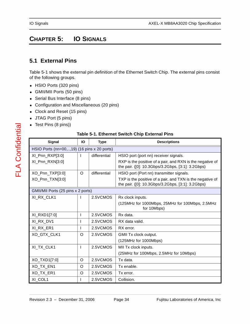
CHAPTER 5: IO SIGNALS 34
5.1 External Pins 34
CHAPTER 6: MECHANICAL DESCRIPTION 38
6.1 Dimensions 386.2 Pin Organization 396.3 Pin Listing 40
Revision 2.3 – December 31, 2006 Page 2 Fujitsu Laboratories of America, Inc
TABLE OF CONTENTS AXEL-X MB8AA3020 Chip SpecificationF
LA C
onfid
entia
l
CHAPTER 7: ELECTRICAL DESCRIPTION 44
7.1 Absolute Maximum Ratings 447.2 Recommended Operating Conditions 447.3 ESD Ratings 457.4 Reference Clock Input (LVDS) Electrical Specifications 457.5 2.5V CMOS IO Electrical Specifications 467.6 HSIO Electrical Specifications 49
7.7 Power Dissipation 517.8 Reset Sequence 51

Introduction AXEL-X MB8AA3020 Chip Specification
Revision 2.3 – December 31, 2006 Page 3 Fujitsu Laboratories of America, Inc
FLA
Con
fiden
tial
CHAPTER 1: INTRODUCTION
1.1 General Description
This specification describes the 4th generation Fujitsu 10Gbps Ethernet switch chip, AXEL-X MB8AA3020. This chip supports twenty 10Gigabit ports which operate at wire speed with high speed IO (HSIO) interfaces. The HSIO interface supports XAUI (802.3ae) and 10GBASE-CX4 (802.3ak). It also supports 10G serial operation to directly connect XFP device. The switch chip has a large shared packet memory inside using our Stream memory technology. The memory realizes multi-port memory using conventional high-density memories as a solution for the mem-ory bandwidth bottleneck in a shared memory switch and provides enough bandwidth required for high performance switch. The switch chip supports congestion management, logical partition-ing, two 1Gigabit ports for easier and superior system design with significantly reduced cost. This chip also has several features such as Jumbo frame support, cut-through and priority queues to achieve higher performance in cluster applications.
1.2 Features
The switch chip has following features:
• Twenty 10Gigabit ports switching operation at wire speed and two 1Gigabit ports• 400Gbps+ aggregate throughput• Integrated SerDes• Support XAUI,10GBASE-CX4, and 10G serial• On-chip Multi-port Stream Memory and buffer management• Cut-through, Priority queues and Jumbo Frame support for high-performance cluster• Jumbo frame (Max. 16KB)• up to 8 Priority queues• Pin-to-pin switching latency of 300nS (including SerDes)• Extended VLAN (up to 64) for Logical Partitioning• Priority PAUSE• Backward Congestion Notification Support• Link aggregation (802.3 clause 43)• IGMP and MLD snooping• DiffServ for IPv4 and IPv6• Deficit Round Robin (DRR) for fair bandwidth sharing• Shaper (CIR: Committed Information Rate)• Meter (PIR: Peak Information Rate)• Port Security (Filtering based on Source MAC address)• Early Detection to avoid blocking

Revision 2.3 – December 31, 2006 Page 4 Fujitsu Laboratories of America, Inc
Introduction AXEL-X MB8AA3020 Chip SpecificationF
LA C
onfid
entia
l
• WAN PHY support• Multiple chip configuration for cluster application• L2 unicast forwarding, address learning and aging• L2 lookup table with 16K MAC address• Shared VLAN Learning (SVL) and Independent VLAN Learning (IVL)• Less MAC Table consumption for IVL• 802.1Q VLAN• VLAN table with 4K VLAN address• User-programmable VLAN Tag Protocol Type• 802.1Q(802.1s) Multiple Spanning Tree• 802.3ae Full-duplex operation using PAUSE flow control• RMON and SMON statistics counters• sFlow (RFC3176) support• EEPROM Interface for initialization• I2C Master Interface for XFP Register Access• Ethernet Interface for housekeeping• External NP support• Port mirroring and VLAN mirroring• 90nm CMOS Technology

Functional Description AXEL-X MB8AA3020 Chip Specification
Revision 2.3 – December 31, 2006 Page 5 Fujitsu Laboratories of America, Inc
FLA
Con
fiden
tial
CHAPTER 2: FUNCTIONAL DESCRIPTION
2.1 Frame Format
The switch chip supports standard Ethernet frames with lengths between 64bytes to 1518bytes(no VLAN), 1522bytes(VLAN) or 1526bytes(User/Extended VLAN Tag) and Jumbo frames with 16Kbytes. The frames less than 64bytes and longer than 16Kbytes are dropped at the input port. The minimum IPG is assumed to be 96bit IDLE plus 64bit preamble. The packets with shorter IPG are not dropped but the wire speed switching is not guaranteed.
2.2 Input Port
Each input port consists of the High speed IO Receiver, Media Access Control (MAC) Receiver and Input Control blocks as shown in Figure 2-1. The High speed IO Receiver performs following functions:
• Physical Interface to XAUI / 10GBASE-CX4 / 10G Serial (PHY)
• Receiver equalization
• Deserialization
• Comma Align, 8B/10B Decoder, Lane Deskew
• XGMII Interface to Media Access Control
Figure 2-1. Input Port
High speed IO Media Access Control(MAC) Receiver block
Input Control Block
Input Buffer
HSIO XGMII Proprietary Interface
HSIO: High Speed IO InterfaceXGMII: 10Gbit Media Independent Interface
Receiver block

Revision 2.3 – December 31, 2006 Page 6 Fujitsu Laboratories of America, Inc
Functional Description AXEL-X MB8AA3020 Chip SpecificationF
LA C
onfid
entia
l
The MAC Receiver performs following IEEE 802.3ae compliant functions:
• XGMII Interface to the High speed block
• Receive PAUSE flow control packet and request the MAC Transmitter to stop sending a new packet
• Frame Check Sequence validation
• Station MAC address matching to detect a management packet designating the switch
• Statistics counters for network management
• Link fault detection
The Input Control performs following protocol dependent and independent functions:
[Protocol Dependent Functions]
• Simple proprietary interface to the MAC Receiver
• Filtering frames based on the Acceptable Frame Type
• Assign the priority based on TOS field (IPv4) / Traffic Class (IPv6) field in the packet.
• Storing the packet temporarily into the Input Buffer
• Request to generate PAUSE flow control packet to the MAC Transmitter if necessary
[Protocol Independent Functions]
• Maintaining the credit for the flow control between the Stream Memory and the Input Control
• Maintaining the free list of the blocks which are assigned to the port
• Checking the credit and store the packet data into the Stream Memory based on the free list.
• Generating a forwarding request to the Central Agent for routing.

Revision 2.3 – December 31, 2006 Page 7 Fujitsu Laboratories of America, Inc
Functional Description AXEL-X MB8AA3020 Chip SpecificationF
LA C
onfid
entia
l
2.3 Central Switching Structure
Figure 2-2 shows the central switching structure for packet buffering and switching. The struc-ture consists of the Multi-port Stream Memory, TAG Memory and the Central Agent. The packet data is stored in the Stream Memory by the Input Control and read from it by the Output Control for an outgoing packet. The control information which shows the next block storing the packet is stored in the TAG Memory.
The Central Agent performs the following protocol independent and dependent functions:
[Protocol Independent Functions]
• Maintains the free list of the blocks which belongs to the buffer pool
• Accept returned blocks from the output ports
• Counting the returned blocks for the multicast
• Generating a request to the Output Control
[Protocol Dependent Functions]
• MAC Address Table and VLAN Table Lookup
• VLAN Ingress Check
• VLAN Egress Filter
• Filtering frames based on port states
• Port Security (Source Address based filtering)
• Link Aggregation
• IGMP/MLD Snooping

Revision 2.3 – December 31, 2006 Page 8 Fujitsu Laboratories of America, Inc
Functional Description AXEL-X MB8AA3020 Chip SpecificationF
LA C
onfid
entia
l
.
Figure 2-2. Central Switching Structure
2.3.1 Multicast Mechanism
AXEL-X chip uses the logical multicast to utilize the packet memory, or Stream Memory effi-ciently. After MAC Address Table lookup, the address pointer is replicated and put into desig-nated output queues. Each output port load the packet from Stream Memory in parallel and send it to the link.
2.3.2 IP Multicast Snooping
To avoid unnecessary traffic in IP Multicast, AXEL-X supports following standard protocols:
• Internet Group Management Protocol (IGMP) for IPv4.
• Multicast Lister Discovery (MLD) for IPv6.
If an incoming frames is Query or Report of membership for IP Multicast, a copy of the frame is forwarded to Management which sets MAC Address Table and destination ports for the MAC address.
TAG Memory
Multi-port Stream Memory
Central Agent
Input Port 0Input Port 1
... ...
Input Port 0Input Port 1
...
Input Port 0Input Port 1
...
Output Port 0Output Port 1
Output Port 0Output Port 1
...
Output Port 0Output Port 1
...
MAC Address Table / VLAN Table
(Data Storage)
(Control Storage)
Revision 2.3 – December 31, 2006 Page 9 Fujitsu Laboratories of America, Inc
Functional Description AXEL-X MB8AA3020 Chip SpecificationF
LA C
onfid
entia
l
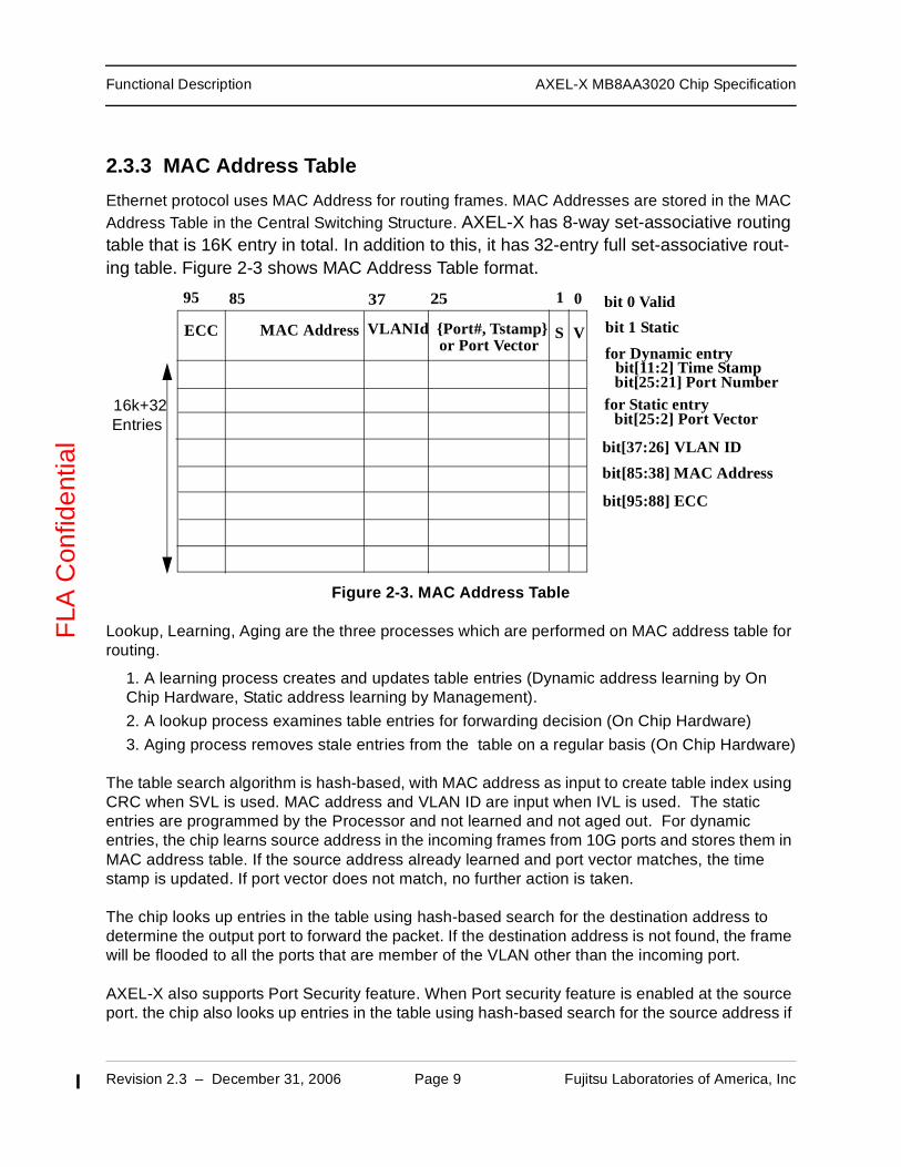
2.3.3 MAC Address Table
Ethernet protocol uses MAC Address for routing frames. MAC Addresses are stored in the MAC Address Table in the Central Switching Structure. AXEL-X has 8-way set-associative routing table that is 16K entry in total. In addition to this, it has 32-entry full set-associative rout-ing table. Figure 2-3 shows MAC Address Table format.
Figure 2-3. MAC Address Table
Lookup, Learning, Aging are the three processes which are performed on MAC address table for routing.
1. A learning process creates and updates table entries (Dynamic address learning by On Chip Hardware, Static address learning by Management).
2. A lookup process examines table entries for forwarding decision (On Chip Hardware)
3. Aging process removes stale entries from the table on a regular basis (On Chip Hardware)
The table search algorithm is hash-based, with MAC address as input to create table index using CRC when SVL is used. MAC address and VLAN ID are input when IVL is used. The static entries are programmed by the Processor and not learned and not aged out. For dynamic entries, the chip learns source address in the incoming frames from 10G ports and stores them in MAC address table. If the source address already learned and port vector matches, the time stamp is updated. If port vector does not match, no further action is taken.
The chip looks up entries in the table using hash-based search for the destination address to determine the output port to forward the packet. If the destination address is not found, the frame will be flooded to all the ports that are member of the VLAN other than the incoming port.
AXEL-X also supports Port Security feature. When Port security feature is enabled at the source port. the chip also looks up entries in the table using hash-based search for the source address if
k
012585
MAC Address
bit 0 Valid
bit 1 Static
for Dynamic entry
bit[37:26] VLAN ID
bit[85:38] MAC Address
ECC VLANId Port#, Tstamp or Port Vector
S V
bit[95:88] ECC
bit[25:21] Port Number
3795
16k+32Entries
bit[11:2] Time Stamp
for Static entrybit[25:2] Port Vector
Revision 2.3 – December 31, 2006 Page 10 Fujitsu Laboratories of America, Inc
Functional Description AXEL-X MB8AA3020 Chip SpecificationF
LA C
onfid
entia
l
it is already learned in the MAC Address Table. If the source address is not found, the frame is forwarded to Processor for further decision and processing. Processor may add the MAC Address in the MAC Address Table if it is ok. Processor may completely shut down the port if it is necessary for security reasons.
Switch chip does aging process to check the stale entries in the table and remove them. If an entry is valid and not updated for a specified time, the aging process clears the valid bit for that entry.
Switch chip provides the table access mechanism for Software on Processor to search, learn or delete an entry in the MAC address table.
Error Protection: ECC
Revision 2.3 – December 31, 2006 Page 11 Fujitsu Laboratories of America, Inc
Functional Description AXEL-X MB8AA3020 Chip SpecificationF
LA C
onfid
entia
l
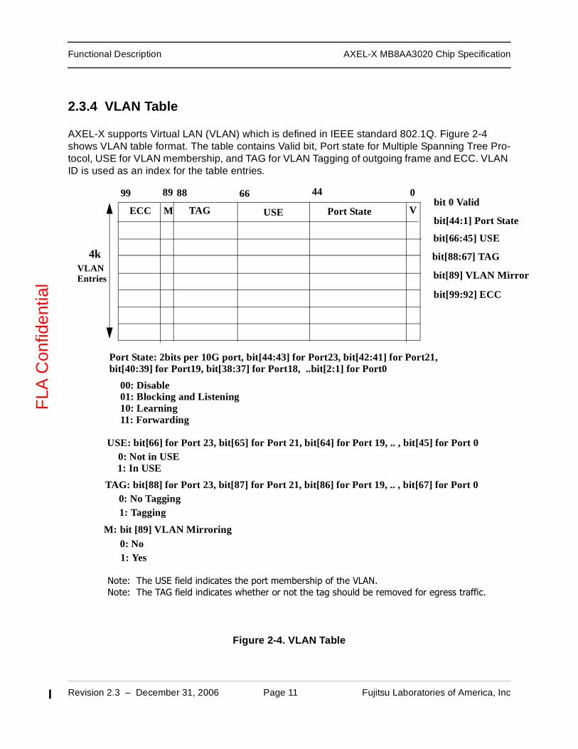
2.3.4 VLAN Table
AXEL-X supports Virtual LAN (VLAN) which is defined in IEEE standard 802.1Q. Figure 2-4 shows VLAN table format. The table contains Valid bit, Port state for Multiple Spanning Tree Pro-tocol, USE for VLAN membership, and TAG for VLAN Tagging of outgoing frame and ECC. VLAN ID is used as an index for the table entries.
Figure 2-4. VLAN Table
USETAG
6688
4kVLANEntries
0
ECC V
8999bit 0 Valid
bit[66:45] USE
bit[88:67] TAG
bit[99:92] ECC
44
bit[44:1] Port State
Port State: 2bits per 10G port, bit[44:43] for Port23, bit[42:41] for Port21,
00: Disable 01: Blocking and Listening 10: Learning 11: Forwarding
USE: bit[66] for Port 23, bit[65] for Port 21, bit[64] for Port 19, .. , bit[45] for Port 0 0: Not in USE 1: In USE
TAG: bit[88] for Port 23, bit[87] for Port 21, bit[86] for Port 19, .. , bit[67] for Port 0 0: No Tagging 1: Tagging
Port StateM
bit[89] VLAN Mirror
bit[40:39] for Port19, bit[38:37] for Port18, ..bit[2:1] for Port0
M: bit [89] VLAN Mirroring 0: No 1: Yes
Note: The USE field indicates the port membership of the VLAN.Note: The TAG field indicates whether or not the tag should be removed for egress traffic.
Revision 2.3 – December 31, 2006 Page 12 Fujitsu Laboratories of America, Inc
Functional Description AXEL-X MB8AA3020 Chip SpecificationF
LA C
onfid
entia
l
Port state in the VLAN table is used when Multiple Spanning Tree Protocol is enabled because the port state is supposed to be VLAN dependent. If Multiple Spanning Tree is not enabled, Port state in the Port Configuration register is used.
Lookup, Learning are the two processes which are performed on VLAN table for routing.
1. A lookup process examines VLAN entries for routing. The flooding frames are sent to the ports which belong to the same VLAN (On Chip Hardware)
2. A learning process creates and updates table entries which define VLAN associations between VLAN ID and the membership (by Management).
Error Protection: ECC
Revision 2.3 – December 31, 2006 Page 13 Fujitsu Laboratories of America, Inc
Functional Description AXEL-X MB8AA3020 Chip SpecificationF
LA C
onfid
entia
l
2.3.5 Reserved Multicast Address
Following Multicast addresses are reserved for special use, for example, STP, GVRP, GMRP, PAUSE, etc.
• 01-80-c2-00-00-00 to 01-80-c2-00-00-10
• 01-80-c2-00-00-20 to 01-80-c2-00-00-2f
In the default configuration, AXEL-X chip handles frames with these reserved multicast addresses as follows:
• Packet received on 10G ports
- If Processor is attached, forward to Processor
- If no Processor is attached, lookup MAC address and VLAN tables and make forwarding decision
• Packet received on Processor port
- Lookup MAC address and VLAN tables and make forwarding decision
AXEL-X also an additional BPDU handling feature to support Provider VLAN (P802.1ad). Using this feature, some BPDU can be transferred as it is between customer peer while other BPDU is terminated by the provider bridge.
Revision 2.3 – December 31, 2006 Page 14 Fujitsu Laboratories of America, Inc
Functional Description AXEL-X MB8AA3020 Chip SpecificationF
LA C
onfid
entia
l
2.3.6 Partitioning
AXEL-X supports Extended VLAN feature to allow logical partitioning of the switch for server blade application This methods supports multiple AXEL-X chips (not limited to two chips).
• Extended VLAN Table (64 entries x 24-bit port-vector)
• Port Default Extended VLAN ID
• Extended VLAN tag handling
+ Extended VLAN is distinguished by a set of programmable VLAN tag.
+ Optionally, Extended VLAN Priority can be added in the VLAN tag.
2.3.7 Link Aggregation
AXEL-X support Link Aggregation (802.3 clause 43) for increased bandwidth and availability. Link Aggregation allows one or more links to be aggregated together to form a Link Aggregation Group (LAG) as if it were a single link. Based on a Distribution algorithm selected, all frames of a given conversation are forwarded to a single port. Distribution algorithm is based on either of DA, SA, DA/SA, Reception port, Src IP, Dest IP, Src/Dest IP, Src Port, Dest Port, Src/Dest Port or VLAN ID. In addition, a tuning mechanism is supported for better load balancing if the number of end stations is small. When a link failure happens in LAG, the conversation can be moved to another link in the LAG.
Revision 2.3 – December 31, 2006 Page 15 Fujitsu Laboratories of America, Inc
Functional Description AXEL-X MB8AA3020 Chip SpecificationF
LA C
onfid
entia
l
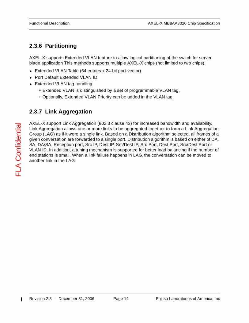
2.4 Output Port
Each output port consists of the Output Control, Media Access Control (MAC) Transmitter and the High speed IO Transmitter blocks as shown in Figure 2-5.
The Output Control performs following protocol independent and protocol dependent functions:
[Protocol Independent Functions]
• Accepting an output request from the Central Agent and puts the request in the output queues
• Arbitrating output requests in the output queues
• Sharing the bandwidth fairly using Deficit Round Robin (DRR)
• Loading the packet data from the Stream Memory
[Protocol Dependent Functions]
• Filtering frames based on VLAN egress rules
• Output the packet data to the MAC Transmitter
• Simple proprietary interface to the MAC Transmitter
Figure 2-5. Output Port
Media Access Control(MAC) Transmitter
Output Control Block
HSIO XGMIIProprietary Interface
HSIO: High Speed IO InterfaceXGMII: 10Gbit Media Independent Interface
High speed IO
blockTransmitter block
Output Queues
Revision 2.3 – December 31, 2006 Page 16 Fujitsu Laboratories of America, Inc
Functional Description AXEL-X MB8AA3020 Chip SpecificationF
LA C
onfid
entia
l
The MAC Transmitter performs following IEEE 802.3ae compliant functions:
• XGMII Interface to the high speed block including PHY register access
• Generate PAUSE flow control packet by a request from the Input Control
• Stop sending a new packet by a request from the MAC receiver
• Frame Check Sequence generation and insertion
• Statistics counters for network management
• Link fault signaling
• WAN-PHY (OC-192) data rate control
The High speed IO Transmitter performs following functions:
• XGMII Interface to Media Access Control
• 8B/10B Encoder
• Serialization
• Transmitter equalization
• XAUI / 10GBASE-CX4 / 10G Serial (PHY) to physical Interface
2.4.1 Scheduling
The codepoint is mapped to a priority using the Priority Mapping Register. The Strict Priority, DRR or Strict+DRR is used for arbitration between 8 priorities. The scheduling is done on packet level.

Revision 2.3 – December 31, 2006 Page 17 Fujitsu Laboratories of America, Inc
Functional Description AXEL-X MB8AA3020 Chip SpecificationF
LA C
onfid
entia
l
2.5 On-chip Code
The On-Chip code communicates with AXEL-X Driver for initialization, handling management protocols, transferring frames, performing MAC address Table, VLAN Table updates and support network management functions.
The management packets to be processed by Management are as follows:
• BPDU for the spanning tree protocol
• GVRP for the virtual LAN
• ICMP for the switch control such as ping
• SNMP for the network management such as statistics monitoring and switch reset
• IGMP / MLD Snooping
• sFLOW
• BCN (Backward Congestion Notification)
Figure 2-6. An Example of Software Configuration
NIC Driver
On-Chip Code API
AXEL-X
AXEL-X On-Chip Code
AXEL-X Driver
API
Layer 2 Software
OS
for Management
Revision 2.3 – December 31, 2006 Page 18 Fujitsu Laboratories of America, Inc
Functional Description AXEL-X MB8AA3020 Chip SpecificationF
LA C
onfid
entia
l
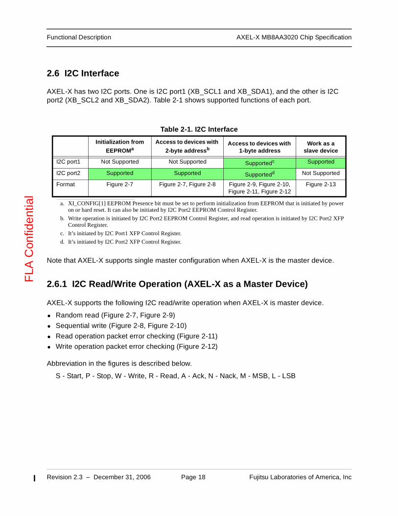
2.6 I2C Interface
AXEL-X has two I2C ports. One is I2C port1 (XB_SCL1 and XB_SDA1), and the other is I2C port2 (XB_SCL2 and XB_SDA2). Table 2-1 shows supported functions of each port.
Note that AXEL-X supports single master configuration when AXEL-X is the master device.
2.6.1 I2C Read/Write Operation (AXEL-X as a Master Device)
AXEL-X supports the following I2C read/write operation when AXEL-X is master device.
• Random read (Figure 2-7, Figure 2-9)
• Sequential write (Figure 2-8, Figure 2-10)
• Read operation packet error checking (Figure 2-11)
• Write operation packet error checking (Figure 2-12)
Abbreviation in the figures is described below.
S - Start, P - Stop, W - Write, R - Read, A - Ack, N - Nack, M - MSB, L - LSB
Table 2-1. I2C Interface
Initialization from
EEPROMa
a. XI_CONFIG[1] EEPROM Presence bit must be set to perform initialization from EEPROM that is initiated by power on or hard reset. It can also be initiated by I2C Port2 EEPROM Control Register.
Access to devices with
2-byte addressb
b. Write operation is initiated by I2C Port2 EEPROM Control Register, and read operation is initiated by I2C Port2 XFP Control Register.
Access to devices with 1-byte address
Work as a slave device
I2C port1 Not Supported Not Supported Supportedc
c. It’s initiated by I2C Port1 XFP Control Register.
Supported
I2C port2 Supported Supported Supportedd
d. It’s initiated by I2C Port2 XFP Control Register.
Not Supported
Format Figure 2-7 Figure 2-7, Figure 2-8 Figure 2-9, Figure 2-10, Figure 2-11, Figure 2-12
Figure 2-13

Revision 2.3 – December 31, 2006 Page 19 Fujitsu Laboratories of America, Inc
Functional Description AXEL-X MB8AA3020 Chip SpecificationF
LA C
onfid
entia
l
Figure 2-7. Random Read (2 bytes address; n bytes data)
Figure 2-8. Sequential Write (2 byte address; n bytes data)
Figure 2-9. Random Read (1 byte address; 1, 2, 4 bytes data)
Figure 2-10. Sequential Write (1 byte address; 1, 2, 4 bytes data)
Master S W M L M L Sx x x x x x x 0 0 x x x x x x x x 0 x x x x x x x x 0 1 0 1 0 0 0 0
Slave A A A
Master R A A N P1 0 x x x x x x x x 0 x x x x x x x x 0 x x x x x x x x 1
Slave A M L M L M L
Memory Address 1DEV Address Memory Address 0 DEV Address
…Data word 0 Data word 1 Data word n
Master S W M L M L
x x x x x x x 0 0 x x x x x x x x 0 x x x x x x x x 0Slave A A A
Master M L M L M L Px x x x x x x x 0 x x x x x x x x 0 x x x x x x x x 0
Slave A A A
Data Word 0 Data Word 1
Memory Address 1
Data Word n …
DEV Address Memory Address 0
Master S W M L S Rx x x x x x x 0 0 x x x x x x x x 0 1 0 1 0 0 0 0 1 0
Slave A A A
Master A A A N Px x x x x x x x 0 x x x x x x x x 0 x x x x x x x x 0 x x x x x x x x 1
Slave M L M L M L M L
DEV Address
Data word 0 Data word 1
DEV Address Memory Address
Data word 3Data word 2
Master S W M L M L
x x x x x x x 0 0 x x x x x x x x 0 x x x x x x x x 0Slave A A A
Master M L M L M L Px x x x x x x x 0 x x x x x x x x 0 x x x x x x x x 0
Slave A A A
Data Word 3Data Word 1 Data Word 2
Memory AddressDEV Address Data Word 0
Revision 2.3 – December 31, 2006 Page 20 Fujitsu Laboratories of America, Inc
Functional Description AXEL-X MB8AA3020 Chip SpecificationF
LA C
onfid
entia
l
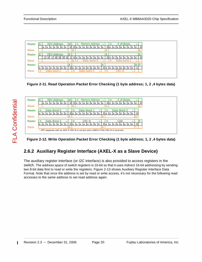
Figure 2-11. Read Operation Packet Error Checking (1 byte address; 1, 2 ,4 bytes data)
Figure 2-12. Write Operation Packet Error Checking (1 byte address; 1, 2 ,4 bytes data)
2.6.2 Auxiliary Register Interface (AXEL-X as a Slave Device)
The auxiliary register interface (or I2C interface) is also provided to access registers in the switch. The address space of switch registers is 16-bit so that it uses indirect 16-bit addressing by sending two 8-bit data first to read or write the registers. Figure 2-13 shows Auxiliary Register Interface Data Format. Note that once the address is set by read or write access, it’s not necessary for the following read accesses to the same address to set read address again.
Master S W M L M L
x x x x x x x 0 0 x x x x x x x x 0 x x x x x x x x 0Slave A A A
Master S R A A1 0 1 0 0 0 0 1 0 x x x x x x x x 0 x x x x x x x x 0
Slave A M L M L
Master A A N Px x x x x x x x 0 x x x x x x x x 0 x x x x x x x x 1
Slave M L M L M LCRC-8
# of BytesDEV Address Memory Address
DEV Address
Data word 0 Data word 1
Data word 2 Data word 3
Master S W M L M L
x x x x x x x 0 0 x x x x x x x x 0 x x x x x x x x 0Slave A A A
Master M L M L M L
x x x x x x x x 0 x x x x x x x x 0 x x x x x x x x 0Slave A A A
Master M L M L M L Px x x x x x x x 0 x x x x x x x x 0 x x x x x x x x 0
Slave A A *
DEV Address Memory Address
Data Word 0
# of Bytes
Data Word 1 Data Word 2
* XFP responds with an ACK if CRC-8 is correct and a NACK if the CRC-8 is incorrect.
Data Word 3 CRC-8 CAB

Revision 2.3 – December 31, 2006 Page 21 Fujitsu Laboratories of America, Inc
Functional Description AXEL-X MB8AA3020 Chip SpecificationF
LA C
onfid
entia
l
.
Figure 2-13. Auxiliary Register Interface Data Format
2.6.3 EEPROM Data Format
The EEPROM Interface is provided for the configuration and initialization of the switch. If there is no EEPROM, the switch is configured and initialized through Auxiliary Register Interface.
Figure 2-14 shows the data formats of the EEPROM of 8bit wide. The EEPROM Interface loads the data based on these formats and writes them into the registers or tables. This procedure repeats until the End of Data is detected. The packet size for Table Data is equal or greater than 8 and depends on the table entry size.
2 Byte Write Set read address.
6 Byte Write Write 32 bit data to the specified 16 bit address.
4 Byte Read Retrieve read data.
DEV SEL is 1010xxxb where lower 3 bits is defined by XI_CONFIG[6:4].
Master S W M L M L P1 0 1 0 0 0 0 0 0 x x x x x x x x 0 x x x x x x x x 0
Slave A A A
DEV Address Memory Address 0 Memory Address 1
Master S W M L M L
x x x x x x x 0 0 x x x x x x x x 0 x x x x x x x x 0Slave A A A
Master M L M L M L M L Px x x x x x x x 0 x x x x x x x x 0 x x x x x x x x 0 x x x x x x x x 0
Slave A A A A
Data Word 2 Data Word 3Data Word 0 Data Word 1
DEV Address Memory Address 0 Memory Address 1
Master S R A1 0 1 0 0 0 0 1 0 x x x x x x x x 0 x x x x x x x x
Slave A M L M L
Master A A N P0 x x x x x x x x 0 x x x x x x x x 1
Slave M L M L
Data word 1
Data word 2
DEV Address
Data word 3
Data word 0
Revision 2.3 – December 31, 2006 Page 22 Fujitsu Laboratories of America, Inc
Functional Description AXEL-X MB8AA3020 Chip SpecificationF
LA C
onfid
entia
l
Figure 2-14. EEPROM Data Format
ex. to write 01020304h into
07h04h00h
00h
04h03h02h01h
General Purpose Register (0004h)
‘00000111’ (Byte length)
Address[7:2] ‘00’
Address[15:8]
Data[7:0]
7 0
0
1
2
Data[15:8]
Data[23:16]
Data[31:24]
3
4
5
6
‘00000000’ (End of Data)7 0
0
Register Data End of Data

Revision 2.3 – December 31, 2006 Page 23 Fujitsu Laboratories of America, Inc
Functional Description AXEL-X MB8AA3020 Chip SpecificationF
LA C
onfid
entia
l
2.7 Initialization
The initialization is a three step processes.
1. Hardware Initialization
2. Load Initialization by EEPROM / Management
3. Port State Initialization using Spanning Tree Protocol (optional)
The hardware initialization includes the followings:
• Internal registers
The all internal registers are initialized to their default values as defined in the Chapter 4.
• TAG Memory
TAG Memory is initialized to store indices which shows the next blocks, that is, address 0 is initialized to 1, address 1 is initialized to 2, and so forth.
• MAC address and VLAN Tables
All entries are initialized as invalid.
• Built In Self Test(BIST)
The load initialization includes the followings:
• Internal registers
The internal registers are initialized based on the configuration.
• MAC address and VLAN Tables
The static entries are loaded and initialized as valid.
The port state initialization using Spanning Tree Protocol includes the followings:
• Port states
The port states can be programmed to be in the port states as required by the spanning tree protocol if this option is enabled.
Network Management AXEL-X MB8AA3020 Chip Specification
Revision 2.3 – December 31, 2006 Page 24 Fujitsu Laboratories of America, Inc
FLA
Con
fiden
tial
CHAPTER 3: NETWORK MANAGEMENT
3.1 Introduction
Switch chip facilitates for collecting management information by using various statistical counters. These counters are accessed by the processor through register access mechanism. The counters support BRIDGE MIB, RMON MIB, SMON MIB, IF MIB, Etherlike MIB. Routine Network Management packet transactions are performed on processor interface between switch chip and processor. Management packet handler provides a mechanism for data transfer.
3.2 Management Information Base (MIB) Counters
Ethernet Switch Chip supports a number of MIB counters for network management. These MIB counters are updated based on data received and transmitted by MAC, Input Control, Output Control, MAC address Table, VLAN table and Processor Interface. These counters are accessed by CPU periodically through the Processor Interface. All counter is defined as 32bit wide regis-ters and actual counter width is specified in the following tables. For the counters with actual width less than 32 bits, unused upper bits are padded by 0.
Table 3-1. Transmit and Receive Counters (per port)
Name Width Description
TRC64 25 bits Transmit and Receive 64 Byte Frame Counter
TRC127 25 bits Transmit and Receive 65 to 127 Byte Frame Counter
TRC255 25 bits Transmit and Receive 128 to 255 Byte Frame Counter
TRC511 25 bits Transmit and Receive 256 to 511 Byte Frame Counters
TRC1000 25 bits Transmit and Receive 512 to 1023 Byte Frame Counters
TRC1500 25 bits Transmit and Receive 1024 to 1518 Byte Frame Counters
TRMGVC 25 bits Transmit and Receive 1519 to 1522 Byte Good VLAN Frame CNT

Revision 2.3 – December 31, 2006 Page 25 Fujitsu Laboratories of America, Inc
Network Management AXEL-X MB8AA3020 Chip SpecificationF
LA C
onfid
entia
l
Table 3-2. Receive Statistics Counters (per port)
Name Width Description
RXBYTC 31 bits Number of Bytes received
RXPKTC 25 bits Number of Packets received
RXFCSC 25 bits Number of FCS errors received
RXMCAC 25 bits Number of Multicast packets
RXBCAC 25 bits Number of Broadcast packets received
RXCFC 16 bits Number of Control frames received
RXPFC 16 bits Number of Pause Frame packets received
RXUOC 16 bits Number of Unknown OP codes received
RXALNC 16 bits Number of Alignment Errors received
RXFLRC 25 bits Number of Frame Length Errors receiveda
a. Length errors are not counted in VLAN Tagged frame.
RXCDEC 25 bits Number of Code Errors received
RXCSEC 16 bits Number of Carrier Sense Errors received
RXUNDC 16 bits Number of Undersize packets received
RXOVRC 25 bits Number of oversize packets received
RXFRGC 16 bits Number of Fragments received
RXJBRC 25 bits Number of Jabbers received
RXDRPC 25 bits Number of packets dropped
RXPFC_Pn (n=0-7) 16 bits Number of received Priority Pause frames with Priority n
RXPFC_TRn (n=0-7) 16 bits Number of transition from “not paused” to “paused” for priority n
Revision 2.3 – December 31, 2006 Page 26 Fujitsu Laboratories of America, Inc
Network Management AXEL-X MB8AA3020 Chip SpecificationF
LA C
onfid
entia
l
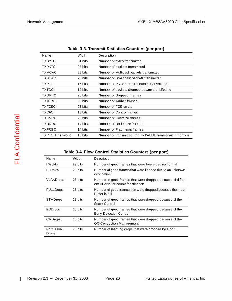
Table 3-3. Transmit Statistics Counters (per port)
Name Width Description
TXBYTC 31 bits Number of bytes transmitted
TXPKTC 25 bits Number of packets transmitted
TXMCAC 25 bits Number of Multicast packets transmitted
TXBCAC 25 bits Number of Broadcast packets transmitted
TXPFC 16 bits Number of PAUSE control frames transmitted
TXTOC 16 bits Number of packets dropped because of Lifetime
TXDRPC 25 bits Number of Dropped frames
TXJBRC 25 bits Number of Jabber frames
TXFCSC 25 bits Number of FCS errors
TXCFC 16 bits Number of Control frames
TXOVRC 25 bits Number of Oversize frames
TXUNDC 14 bits Number of Undersize frames
TXFRGC 14 bits Number of Fragments frames
TXPFC_Pn (n=0-7) 16 bits Number of transmitted Priority PAUSE frames with Priority n
Table 3-4. Flow Control Statistics Counters (per port)
Name Width Description
FWpkts 29 bits Number of good frames that were forwarded as normal
FLDpkts 25 bits Number of good frames that were flooded due to an unknown destination
VLANDrops 25 bits Number of good frames that were dropped because of differ-ent VLANs for source/destination
FULLDrops 25 bits Number of good frames that were dropped because the Input Buffer is full
STMDrops 25 bits Number of good frames that were dropped because of the Storm Control
EDDrops 25 bits Number of good frames that were dropped because of the Early Detection Control
CMDrops 25 bits Number of good frames that were dropped because of the OQ Congestion Management
PortLearn-Drops
25 bits Number of learning drops that were dropped by a port.
Revision 2.3 – December 31, 2006 Page 27 Fujitsu Laboratories of America, Inc
Network Management AXEL-X MB8AA3020 Chip SpecificationF
LA C
onfid
entia
l
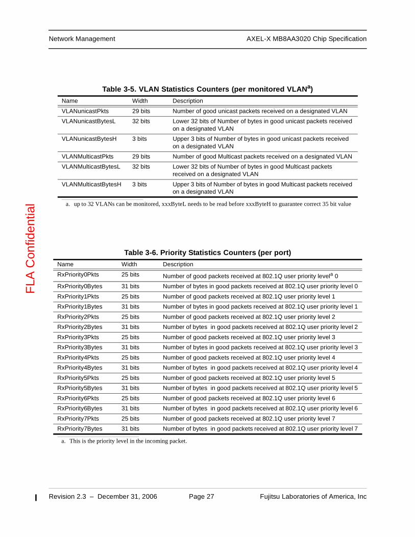
Table 3-5. VLAN Statistics Counters (per monitored VLANa)
a. up to 32 VLANs can be monitored, xxxByteL needs to be read before xxxByteH to guarantee correct 35 bit value
Name Width Description
VLANunicastPkts 29 bits Number of good unicast packets received on a designated VLAN
VLANunicastBytesL 32 bits Lower 32 bits of Number of bytes in good unicast packets received on a designated VLAN
VLANunicastBytesH 3 bits Upper 3 bits of Number of bytes in good unicast packets received on a designated VLAN
VLANMulticastPkts 29 bits Number of good Multicast packets received on a designated VLAN
VLANMulticastBytesL 32 bits Lower 32 bits of Number of bytes in good Multicast packets received on a designated VLAN
VLANMulticastBytesH 3 bits Upper 3 bits of Number of bytes in good Multicast packets received on a designated VLAN
Table 3-6. Priority Statistics Counters (per port)
Name Width Description
RxPriority0Pkts 25 bits Number of good packets received at 802.1Q user priority levela 0
a. This is the priority level in the incoming packet.
RxPriority0Bytes 31 bits Number of bytes in good packets received at 802.1Q user priority level 0
RxPriority1Pkts 25 bits Number of good packets received at 802.1Q user priority level 1
RxPriority1Bytes 31 bits Number of bytes in good packets received at 802.1Q user priority level 1
RxPriority2Pkts 25 bits Number of good packets received at 802.1Q user priority level 2
RxPriority2Bytes 31 bits Number of bytes in good packets received at 802.1Q user priority level 2
RxPriority3Pkts 25 bits Number of good packets received at 802.1Q user priority level 3
RxPriority3Bytes 31 bits Number of bytes in good packets received at 802.1Q user priority level 3
RxPriority4Pkts 25 bits Number of good packets received at 802.1Q user priority level 4
RxPriority4Bytes 31 bits Number of bytes in good packets received at 802.1Q user priority level 4
RxPriority5Pkts 25 bits Number of good packets received at 802.1Q user priority level 5
RxPriority5Bytes 31 bits Number of bytes in good packets received at 802.1Q user priority level 5
RxPriority6Pkts 25 bits Number of good packets received at 802.1Q user priority level 6
RxPriority6Bytes 31 bits Number of bytes in good packets received at 802.1Q user priority level 6
RxPriority7Pkts 25 bits Number of good packets received at 802.1Q user priority level 7
RxPriority7Bytes 31 bits Number of bytes in good packets received at 802.1Q user priority level 7
Revision 2.3 – December 31, 2006 Page 28 Fujitsu Laboratories of America, Inc
Network Management AXEL-X MB8AA3020 Chip SpecificationF
LA C
onfid
entia
l
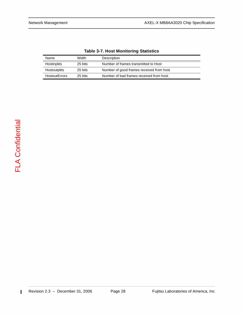
Table 3-7. Host Monitoring Statistics
Name Width Description
Hostinpkts 25 bits Number of frames transmitted to Host
Hostoutpkts 25 bits Number of good frames received from host
HostoutErrors 25 bits Number of bad frames received from host.
Revision 2.3 – December 31, 2006 Page 29 Fujitsu Laboratories of America, Inc
Network Management AXEL-X MB8AA3020 Chip SpecificationF
LA C
onfid
entia
l
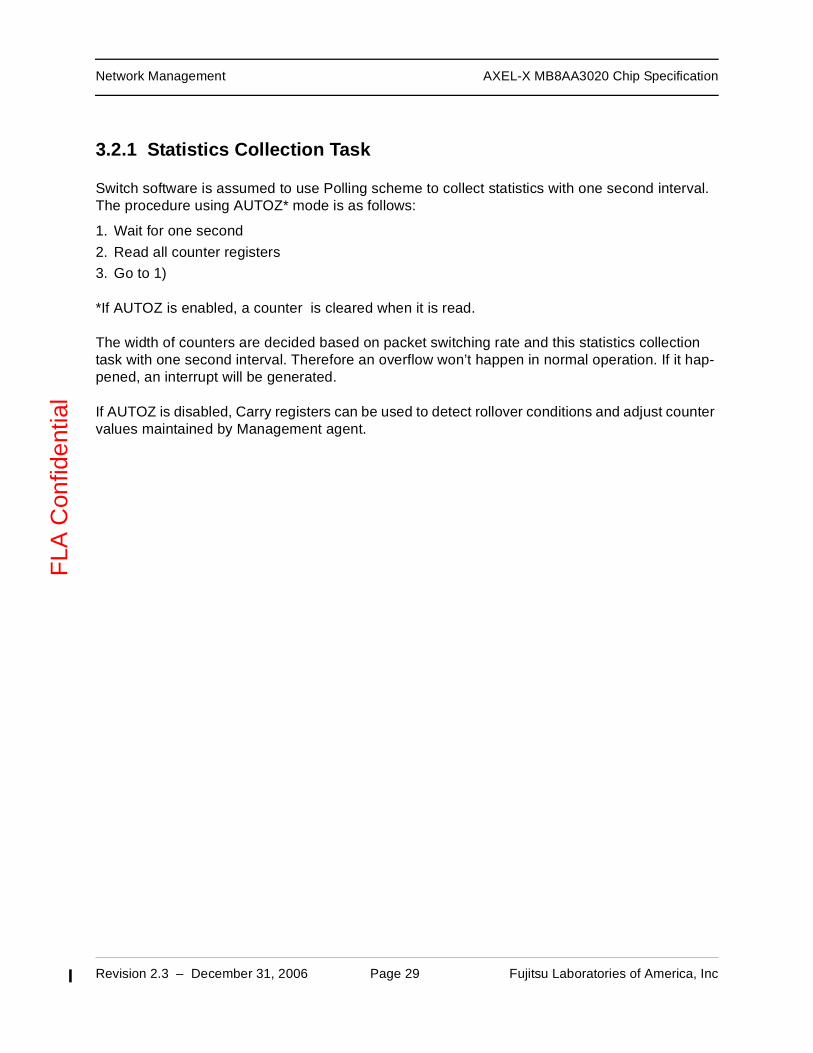
3.2.1 Statistics Collection Task
Switch software is assumed to use Polling scheme to collect statistics with one second interval. The procedure using AUTOZ* mode is as follows:
1. Wait for one second
2. Read all counter registers
3. Go to 1)
*If AUTOZ is enabled, a counter is cleared when it is read.
The width of counters are decided based on packet switching rate and this statistics collection task with one second interval. Therefore an overflow won’t happen in normal operation. If it hap-pened, an interrupt will be generated.
If AUTOZ is disabled, Carry registers can be used to detect rollover conditions and adjust counter values maintained by Management agent.

Error Handling AXEL-X MB8AA3020 Chip Specification
Revision 2.3 – December 31, 2006 Page 30 Fujitsu Laboratories of America, Inc
FLA
Con
fiden
tial
CHAPTER 4: ERROR HANDLING
4.1 Introduction
This chapter describes how the AXEL-X chip handles errors. There are five categories of errors:
• Input errors
• Bridge errors
• Output errors
• Hardware errors
• Software errors
These error groups are described in the following sections.
The error level is defined as follows:
F: FatalNFC: Non Fatal CorrectableNFU: Non Fatal Uncorrectable
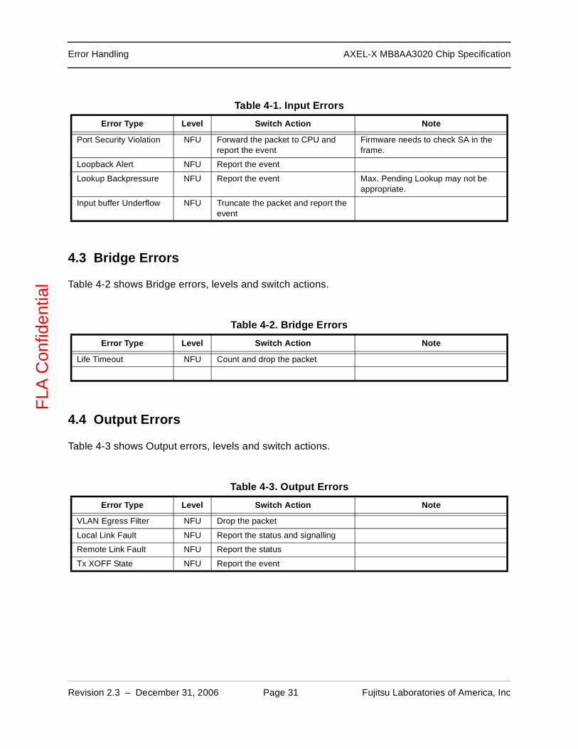
4.2 Input Errors
Table 4-1 shows Input errors, levels and switch actions.
Table 4-1. Input Errors
Error Type Level Switch Action Note
Local Link Fault NFU Report the status
Remote Link Fault NFU Report the status
Symbol Error NFU Count and drop the packet
Alignment Error NFU Count and drop the packet
Length Error NFU Count and drop the packet
FCS Error NFU Count and drop the packet or abort the transmission of the packet.
Input buffer Full NFU Drop incoming packet
Acceptable Frame Filter NFU Count and drop the packet
Storm Control NFU Drop the packet
VLAN Ingress Check NFU Drop the packet
VLAN Filter Hit NFU Drop the packet and report the event
VLAN setting may not be correct.
Revision 2.3 – December 31, 2006 Page 31 Fujitsu Laboratories of America, Inc
Error Handling AXEL-X MB8AA3020 Chip SpecificationF
LA C
onfid
entia
l
4.3 Bridge Errors
Table 4-2 shows Bridge errors, levels and switch actions.
4.4 Output Errors
Table 4-3 shows Output errors, levels and switch actions.
Port Security Violation NFU Forward the packet to CPU and report the event
Firmware needs to check SA in the frame.
Loopback Alert NFU Report the event
Lookup Backpressure NFU Report the event Max. Pending Lookup may not be appropriate.
Input buffer Underflow NFU Truncate the packet and report the event
Table 4-2. Bridge Errors
Error Type Level Switch Action Note
Life Timeout NFU Count and drop the packet
Table 4-3. Output Errors
Error Type Level Switch Action Note
VLAN Egress Filter NFU Drop the packet
Local Link Fault NFU Report the status and signalling
Remote Link Fault NFU Report the status
Tx XOFF State NFU Report the event
Table 4-1. Input Errors
Error Type Level Switch Action Note

Revision 2.3 – December 31, 2006 Page 32 Fujitsu Laboratories of America, Inc
Error Handling AXEL-X MB8AA3020 Chip SpecificationF
LA C
onfid
entia
l
4.5 Hardware Errors
Table 4-4 shows Hardware errors, levels and switch actions.
4.6 Software Errors
Table 4-5 shows Software errors, levels and switch actions.
Table 4-4. Hardware Errors
Error Type Level Switch Action Note
CM Buffer MBE F Log and report the event need chip reset
Tag Memory MBE F Log and report the event need chip reset
Drop Queue MBE F Report the event need chip reset
Output Queue MBE F Report the event need chip reset
IBUF Tag MBE NFU Report the event need port reset
MAC Address Table MBE NFU Log and report the event need to delete the entry
VLAN Table MBE NFU Log and report the event need to delete the entry
MST MBE NFU Log, count and report the event if error count becomes large, need chip reset
Stream Memory Tag MBE NFU Report the event
CM Buffer SBE NFC Log and report the event
Tag Memory SBE NFC Log and report the event. Writeback when SBE Writeback is enabled.
Drop Queue SBE NFC Report the event
Output Queue SBE NFC Report the event
IBUF Tag SBE NFC Report the event
MAC Address Table SBE NFC Report the event
VLAN Table SBE NFC Log and report the event. Writeback when SBE Writeback is enabled.
MST SBE NFC Log and report the event. Writeback when SBE Writeback is enabled.
Stream Memory Tag SBE NFC Report the event
Table 4-5. Software Errors
Error Type Level Switch Action Note

Revision 2.3 – December 31, 2006 Page 33 Fujitsu Laboratories of America, Inc
Error Handling AXEL-X MB8AA3020 Chip SpecificationF
LA C
onfid
entia
l
IO Signals AXEL-X MB8AA3020 Chip Specification
Revision 2.3 – December 31, 2006 Page 34 Fujitsu Laboratories of America, Inc
FLA
Con
fiden
tial
CHAPTER 5: IO SIGNALS
5.1 External Pins
Table 5-1 shows the external pin definition of the Ethernet Switch Chip. The external pins consist of the following groups.
• HSIO Ports (320 pins)
• GMII/MII Ports (50 pins)
• Serial Bus Interface (8 pins)
• Configuration and Miscellaneous (20 pins)
• Clock and Reset (15 pins)
• JTAG Port (5 pins)
• Test Pins (8 pins))
Table 5-1. Ethernet Switch Chip External Pins
Signal IO Type Descriptions
HSIO Ports (nn=00,..,19) (16 pins x 20 ports)
XI_Pnn_RXP[3:0]
XI_Pnn_RXN[3:0]
I differential HSIO port (port nn) receiver signals.
RXP is the positive of a pair, and RXN is the negative of the pair. ([0]: 10.3Gbps/3.2Gbps, [3:1]: 3.2Gbps)
XO_Pnn_TXP[3:0]
XO_Pnn_TXN[3:0]
O differential HSIO port (Port nn) transmitter signals.
TXP is the positive of a pair, and TXN is the negative of the pair. ([0]: 10.3Gbps/3.2Gbps, [3:1]: 3.2Gbps)
GMII/MII Ports (25 pins x 2 ports)
XI_RX_CLK1 I 2.5VCMOS Rx clock inputs.
(125MHz for 1000Mbps, 25MHz for 100Mbps, 2.5MHz for 10Mbps)
XI_RXD1[7:0] I 2.5VCMOS Rx data.
XI_RX_DV1 I 2.5VCMOS RX data valid.
XI_RX_ER1 I 2.5VCMOS RX error.
XO_GTX_CLK1 O 2.5VCMOS GMII Tx clock output.
(125MHz for 1000Mbps)
XI_TX_CLK1 I 2.5VCMOS MII Tx clock inputs.
(25MHz for 100Mbps, 2.5MHz for 10Mbps)
XO_TXD1[7:0] O 2.5VCMOS Tx data.
XO_TX_EN1 O 2.5VCMOS Tx enable.
XO_TX_ER1 O 2.5VCMOS Tx error.
XI_COL1 I 2.5VCMOS Collision.

Revision 2.3 – December 31, 2006 Page 35 Fujitsu Laboratories of America, Inc
IO Signals AXEL-X MB8AA3020 Chip SpecificationF
LA C
onfid
entia
l
XI_CRS1 I 2.5VCMOS Carrier sense.
XI_RX_CLK2 I 2.5VCMOS Rx clock inputs.
(125MHz for 1000Mbps, 25MHz for 100Mbps, 2.5MHz for 10Mbps)
XI_RXD2[7:0] I 2.5VCMOS Rx data.
XI_RX_DV2 I 2.5VCMOS RX data valid.
XI_RX_ER2 I 2.5VCMOS RX error.
XO_GTX_CLK2 O 2.5VCMOS GMII Tx clock output.
(125MHz for 1000Mbps)
XI_TX_CLK2 I 2.5VCMOS MII Tx clock inputs.
(25MHz for 100Mbps, 2.5MHz for 10Mbps)
XO_TXD2[7:0] O 2.5VCMOS Tx data.
XO_TX_EN2 O 2.5VCMOS Tx enable.
XO_TX_ER2 O 2.5VCMOS Tx error.
XI_COL2 I 2.5VCMOS Collision.
XI_CRS2 I 2.5VCMOS Carrier sense.
Serial Bus Interface (8 pins)
XB_SCL1 IO 2.5VCMOS (O/D)
I2C port 1 clock line.
XB_SDA1 IO 2.5VCMOS (O/D)
I2C port 1 data line.
XB_SCL2 IO 2.5VCMOS (O/D)
I2C port 2 clock line.
XB_SDA2 IO 2.5VCMOS (O/D)
I2C port 2 data line.
XO_MDC1 O 2.5VCMOS MDIO port 1 clock line.
XB_MDIO1 IO 2.5VCMOS (O/D)
MDIO port 1 data line.
XO_MDC2 O 2.5VCMOS MDIO port 2 clock line.
XB_MDIO2 IO 2.5VCMOS (O/D)
MDIO port 2 data line.
Table 5-1. Ethernet Switch Chip External Pins (Cont’d.)
Signal IO Type Descriptions
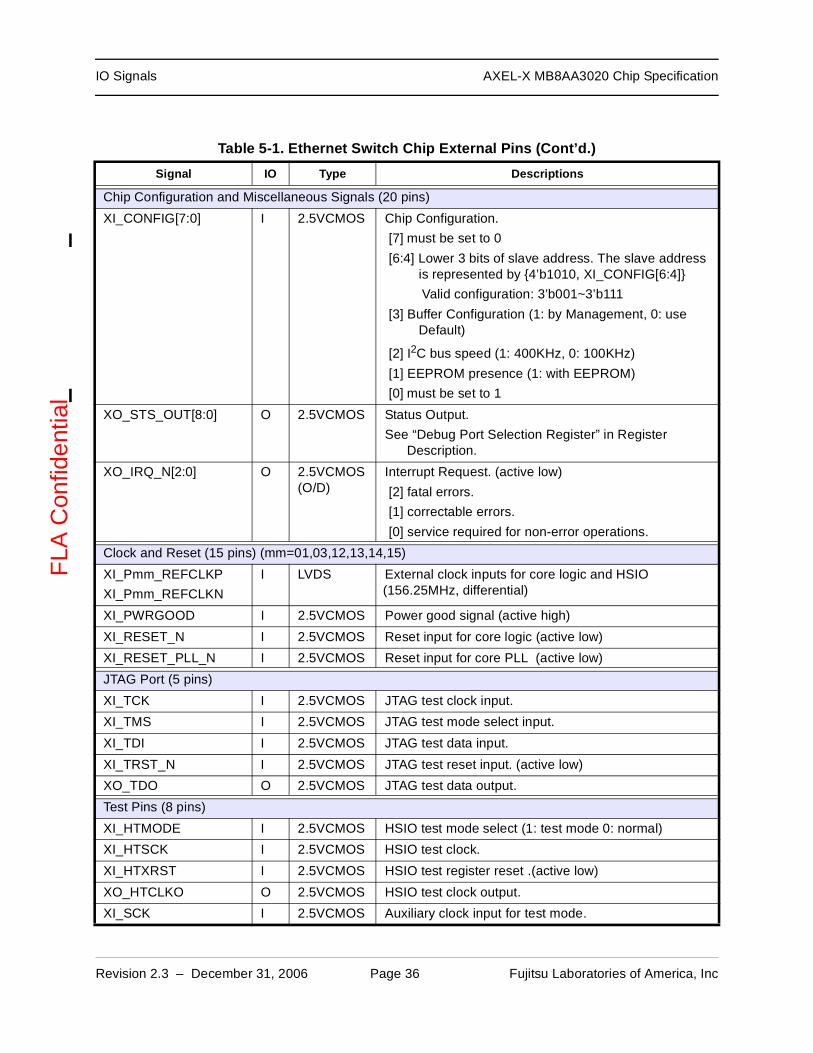
Revision 2.3 – December 31, 2006 Page 36 Fujitsu Laboratories of America, Inc
IO Signals AXEL-X MB8AA3020 Chip SpecificationF
LA C
onfid
entia
l
Chip Configuration and Miscellaneous Signals (20 pins)
XI_CONFIG[7:0] I 2.5VCMOS Chip Configuration.
[7] must be set to 0
[6:4] Lower 3 bits of slave address. The slave address is represented by 4’b1010, XI_CONFIG[6:4]
Valid configuration: 3’b001~3’b111
[3] Buffer Configuration (1: by Management, 0: use Default)
[2] I2C bus speed (1: 400KHz, 0: 100KHz)
[1] EEPROM presence (1: with EEPROM)
[0] must be set to 1
XO_STS_OUT[8:0] O 2.5VCMOS Status Output.
See “Debug Port Selection Register” in Register Description.
XO_IRQ_N[2:0] O 2.5VCMOS (O/D)
Interrupt Request. (active low)
[2] fatal errors.
[1] correctable errors.
[0] service required for non-error operations.
Clock and Reset (15 pins) (mm=01,03,12,13,14,15)
XI_Pmm_REFCLKP
XI_Pmm_REFCLKN
I LVDS External clock inputs for core logic and HSIO (156.25MHz, differential)
XI_PWRGOOD I 2.5VCMOS Power good signal (active high)
XI_RESET_N I 2.5VCMOS Reset input for core logic (active low)
XI_RESET_PLL_N I 2.5VCMOS Reset input for core PLL (active low)
JTAG Port (5 pins)
XI_TCK I 2.5VCMOS JTAG test clock input.
XI_TMS I 2.5VCMOS JTAG test mode select input.
XI_TDI I 2.5VCMOS JTAG test data input.
XI_TRST_N I 2.5VCMOS JTAG test reset input. (active low)
XO_TDO O 2.5VCMOS JTAG test data output.
Test Pins (8 pins)
XI_HTMODE I 2.5VCMOS HSIO test mode select (1: test mode 0: normal)
XI_HTSCK I 2.5VCMOS HSIO test clock.
XI_HTXRST I 2.5VCMOS HSIO test register reset .(active low)
XO_HTCLKO O 2.5VCMOS HSIO test clock output.
XI_SCK I 2.5VCMOS Auxiliary clock input for test mode.
Table 5-1. Ethernet Switch Chip External Pins (Cont’d.)
Signal IO Type Descriptions
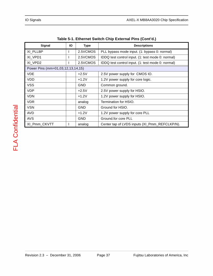
Revision 2.3 – December 31, 2006 Page 37 Fujitsu Laboratories of America, Inc
IO Signals AXEL-X MB8AA3020 Chip SpecificationF
LA C
onfid
entia
l
XI_PLLBP I 2.5VCMOS PLL bypass mode input. (1: bypass 0: normal)
XI_VPD1 I 2.5VCMOS IDDQ test control input. (1: test mode 0: normal)
XI_VPD2 I 2.5VCMOS IDDQ test control input. (1: test mode 0: normal)
Power Pins (mm=01,03,12,13,14,15)
VDE +2.5V 2.5V power supply for CMOS IO.
VDD +1.2V 1.2V power supply for core logic.
VSS GND Common ground.
VDP +2.5V 2.5V power supply for HSIO.
VDN +1.2V 1.2V power supply for HSIO.
VDR analog Termination for HSIO.
VSN GND Ground for HSIO.
AVD +1.2V 1.2V power supply for core PLL
AVS GND Ground.for core PLL
XI_Pmm_CKVTT I analog Center tap of LVDS inputs (XI_Pmm_REFCLKP/N).
Table 5-1. Ethernet Switch Chip External Pins (Cont’d.)
Signal IO Type Descriptions

Mechanical Description AXEL-X MB8AA3020 Chip Specification
Revision 2.3 – December 31, 2006 Page 38 Fujitsu Laboratories of America, Inc
FLA
Con
fiden
tial
CHAPTER 6: MECHANICAL DESCRIPTION
This chapter describes the pin assignments and the mechanical specifications.
6.1 Dimensions
The mechanical specifications are shown in Table 6-1.
Figure 6-1. Drawing Details for FCBGA1156
Table 6-1. Package information
Parameter Value
Package type FC-BGA (Flip Chip Ball Grid Array)
Total pin count 1156
Package size 35 x 35 sq mm
Ball pitch 1.0 mm
Thermal Resistance
(deg.C/W)
θjc = 0.73
θja = 8.45 (0 m/s air), 6.67 (1 m/s air), 4.45 (3 m/s air)
Drawing details for FCBGA1156 Preliminary & Confidential
Dimensions in millimeters

Revision 2.3 – December 31, 2006 Page 39 Fujitsu Laboratories of America, Inc
Mechanical Description AXEL-X MB8AA3020 Chip SpecificationF
LA C
onfid
entia
l
6.2 Pin Organization
Figure 6-2. Package Pins
AXEL-X package pins Version 08 [01/19/2006]
B O TTO M VIEW FC BG A1156index A B C D E F G H J K L M N P R T U V W Y AA AB AC AD AE AF AG A H A J AK AL AM AN AP
1234
56789
1011121314151617181920212223242526272829
3031323334
VSS (G nd)VD D (1.2V) chip peripheralVD E (2.5V, IO )VSN (G nd for HSIO ) C hip Area
VD P (2.5V for H SIO )VD N (1.2V for HSIO )VD R (0.8V, Term ination for HSIO )differential (HSIO )differential (clock)single-ended HSIO Port
core side
TX1-
TX1+
TX3-
TX3+
TX0-
TX0+
TX2-
TX2+
RX0+
RX3-
RX2-
RX2+
RX0-
RX3+
RX1-
RX1+
Revision 2.3 – December 31, 2006 Page 40 Fujitsu Laboratories of America, Inc
Mechanical Description AXEL-X MB8AA3020 Chip SpecificationF
LA C
onfid
entia
l
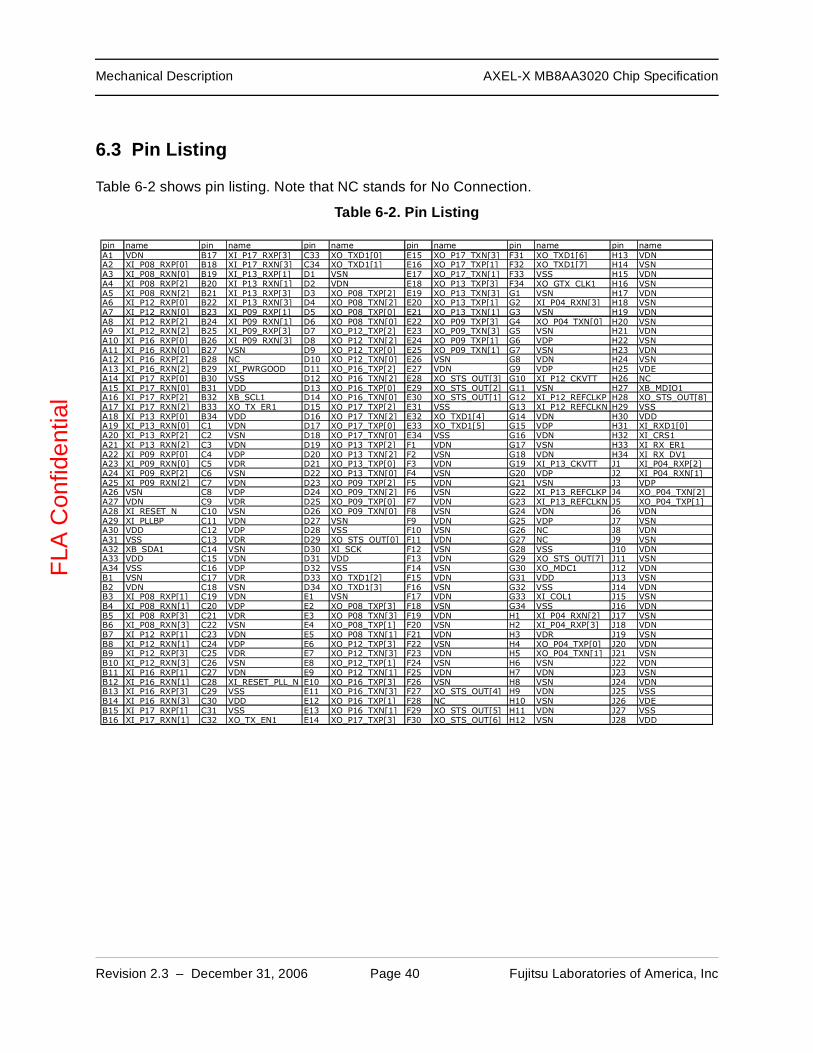
6.3 Pin Listing
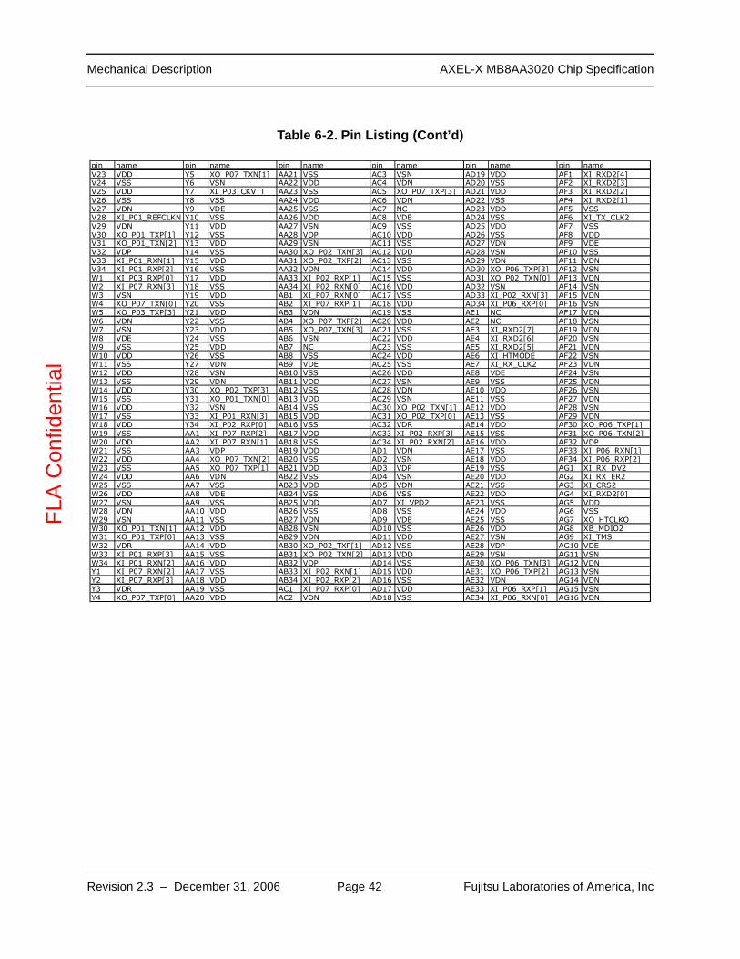
Table 6-2 shows pin listing. Note that NC stands for No Connection.
Table 6-2. Pin Listing
pin name pin name pin name pin name pin name pin nameA1 VDN B17 XI_P17_RXP[3] C33 XO_TXD1[0] E15 XO_P17_TXN[3] F31 XO_TXD1[6] H13 VDNA2 XI_P08_RXP[0] B18 XI_P17_RXN[3] C34 XO_TXD1[1] E16 XO_P17_TXP[1] F32 XO_TXD1[7] H14 VSNA3 XI_P08_RXN[0] B19 XI_P13_RXP[1] D1 VSN E17 XO_P17_TXN[1] F33 VSS H15 VDNA4 XI_P08_RXP[2] B20 XI_P13_RXN[1] D2 VDN E18 XO_P13_TXP[3] F34 XO_GTX_CLK1 H16 VSNA5 XI_P08_RXN[2] B21 XI_P13_RXP[3] D3 XO_P08_TXP[2] E19 XO_P13_TXN[3] G1 VSN H17 VDNA6 XI_P12_RXP[0] B22 XI_P13_RXN[3] D4 XO_P08_TXN[2] E20 XO_P13_TXP[1] G2 XI_P04_RXN[3] H18 VSNA7 XI_P12_RXN[0] B23 XI_P09_RXP[1] D5 XO_P08_TXP[0] E21 XO_P13_TXN[1] G3 VSN H19 VDNA8 XI_P12_RXP[2] B24 XI_P09_RXN[1] D6 XO_P08_TXN[0] E22 XO_P09_TXP[3] G4 XO_P04_TXN[0] H20 VSNA9 XI_P12_RXN[2] B25 XI_P09_RXP[3] D7 XO_P12_TXP[2] E23 XO_P09_TXN[3] G5 VSN H21 VDNA10 XI_P16_RXP[0] B26 XI_P09_RXN[3] D8 XO_P12_TXN[2] E24 XO_P09_TXP[1] G6 VDP H22 VSNA11 XI_P16_RXN[0] B27 VSN D9 XO_P12_TXP[0] E25 XO_P09_TXN[1] G7 VSN H23 VDNA12 XI_P16_RXP[2] B28 NC D10 XO_P12_TXN[0] E26 VSN G8 VDN H24 VSNA13 XI_P16_RXN[2] B29 XI_PWRGOOD D11 XO_P16_TXP[2] E27 VDN G9 VDP H25 VDEA14 XI_P17_RXP[0] B30 VSS D12 XO_P16_TXN[2] E28 XO_STS_OUT[3] G10 XI_P12_CKVTT H26 NCA15 XI_P17_RXN[0] B31 VDD D13 XO_P16_TXP[0] E29 XO_STS_OUT[2] G11 VSN H27 XB_MDIO1A16 XI_P17_RXP[2] B32 XB_SCL1 D14 XO_P16_TXN[0] E30 XO_STS_OUT[1] G12 XI_P12_REFCLKP H28 XO_STS_OUT[8]A17 XI_P17_RXN[2] B33 XO_TX_ER1 D15 XO_P17_TXP[2] E31 VSS G13 XI_P12_REFCLKN H29 VSSA18 XI_P13_RXP[0] B34 VDD D16 XO_P17_TXN[2] E32 XO_TXD1[4] G14 VDN H30 VDDA19 XI_P13_RXN[0] C1 VDN D17 XO_P17_TXP[0] E33 XO_TXD1[5] G15 VDP H31 XI_RXD1[0]A20 XI_P13_RXP[2] C2 VSN D18 XO_P17_TXN[0] E34 VSS G16 VDN H32 XI_CRS1A21 XI_P13_RXN[2] C3 VDN D19 XO_P13_TXP[2] F1 VDN G17 VSN H33 XI_RX_ER1A22 XI_P09_RXP[0] C4 VDP D20 XO_P13_TXN[2] F2 VSN G18 VDN H34 XI_RX_DV1A23 XI_P09_RXN[0] C5 VDR D21 XO_P13_TXP[0] F3 VDN G19 XI_P13_CKVTT J1 XI_P04_RXP[2]A24 XI_P09_RXP[2] C6 VSN D22 XO_P13_TXN[0] F4 VSN G20 VDP J2 XI_P04_RXN[1]A25 XI_P09_RXN[2] C7 VDN D23 XO_P09_TXP[2] F5 VDN G21 VSN J3 VDPA26 VSN C8 VDP D24 XO_P09_TXN[2] F6 VSN G22 XI_P13_REFCLKP J4 XO_P04_TXN[2]A27 VDN C9 VDR D25 XO_P09_TXP[0] F7 VDN G23 XI_P13_REFCLKN J5 XO_P04_TXP[1]A28 XI_RESET_N C10 VSN D26 XO_P09_TXN[0] F8 VSN G24 VDN J6 VDNA29 XI_PLLBP C11 VDN D27 VSN F9 VDN G25 VDP J7 VSNA30 VDD C12 VDP D28 VSS F10 VSN G26 NC J8 VDNA31 VSS C13 VDR D29 XO_STS_OUT[0] F11 VDN G27 NC J9 VSNA32 XB_SDA1 C14 VSN D30 XI_SCK F12 VSN G28 VSS J10 VDNA33 VDD C15 VDN D31 VDD F13 VDN G29 XO_STS_OUT[7] J11 VSNA34 VSS C16 VDP D32 VSS F14 VSN G30 XO_MDC1 J12 VDNB1 VSN C17 VDR D33 XO_TXD1[2] F15 VDN G31 VDD J13 VSNB2 VDN C18 VSN D34 XO_TXD1[3] F16 VSN G32 VSS J14 VDNB3 XI_P08_RXP[1] C19 VDN E1 VSN F17 VDN G33 XI_COL1 J15 VSNB4 XI_P08_RXN[1] C20 VDP E2 XO_P08_TXP[3] F18 VSN G34 VSS J16 VDNB5 XI_P08_RXP[3] C21 VDR E3 XO_P08_TXN[3] F19 VDN H1 XI_P04_RXN[2] J17 VSNB6 XI_P08_RXN[3] C22 VSN E4 XO_P08_TXP[1] F20 VSN H2 XI_P04_RXP[3] J18 VDNB7 XI_P12_RXP[1] C23 VDN E5 XO_P08_TXN[1] F21 VDN H3 VDR J19 VSNB8 XI_P12_RXN[1] C24 VDP E6 XO_P12_TXP[3] F22 VSN H4 XO_P04_TXP[0] J20 VDNB9 XI_P12_RXP[3] C25 VDR E7 XO_P12_TXN[3] F23 VDN H5 XO_P04_TXN[1] J21 VSNB10 XI_P12_RXN[3] C26 VSN E8 XO_P12_TXP[1] F24 VSN H6 VSN J22 VDNB11 XI_P16_RXP[1] C27 VDN E9 XO_P12_TXN[1] F25 VDN H7 VDN J23 VSNB12 XI_P16_RXN[1] C28 XI_RESET_PLL_N E10 XO_P16_TXP[3] F26 VSN H8 VSN J24 VDNB13 XI_P16_RXP[3] C29 VSS E11 XO_P16_TXN[3] F27 XO_STS_OUT[4] H9 VDN J25 VSSB14 XI_P16_RXN[3] C30 VDD E12 XO_P16_TXP[1] F28 NC H10 VSN J26 VDEB15 XI_P17_RXP[1] C31 VSS E13 XO_P16_TXN[1] F29 XO_STS_OUT[5] H11 VDN J27 VSSB16 XI_P17_RXN[1] C32 XO_TX_EN1 E14 XO_P17_TXP[3] F30 XO_STS_OUT[6] H12 VSN J28 VDD

Revision 2.3 – December 31, 2006 Page 41 Fujitsu Laboratories of America, Inc
Mechanical Description AXEL-X MB8AA3020 Chip SpecificationF
LA C
onfid
entia
l
Table 6-2. Pin Listing (Cont’d)
pin name pin name pin name pin name pin name pin nameJ29 XI_TX_CLK1 L11 VSS M27 VDE P9 VDD R25 VSS U7 XI_P03_REFCLKNJ30 VSS L12 VDD M28 AVD P10 VSS R26 VDE U8 VDNJ31 XI_RXD1[1] L13 VSS M29 VDN P11 VDD R27 VSS U9 VSSJ32 XI_RXD1[2] L14 VDD M30 XO_P05_TXP[3] P12 VSS R28 XI_P01_CKVTT U10 VDDJ33 XI_RXD1[3] L15 VSS M31 VDN P13 VDD R29 VSN U11 VSSJ34 XI_RXD1[4] L16 VDD M32 VSN P14 VSS R30 XO_P05_TXN[1] U12 VDDK1 XI_P04_RXN[0] L17 VSS M33 VDN P15 VDD R31 XO_P05_TXP[0] U13 VSSK2 XI_P04_RXP[1] L18 VDD M34 XI_P05_RXP[0] P16 VSS R32 VDR U14 VDDK3 VDN L19 VSS N1 XI_P00_RXP[2] P17 VDD R33 XI_P05_RXP[3] U15 VSSK4 XO_P04_TXP[2] L20 VDD N2 XI_P00_RXN[1] P18 VSS R34 XI_P05_RXN[2] U16 VDDK5 XO_P04_TXN[3] L21 VSS N3 VDP P19 VDD T1 XI_P03_RXN[2] U17 VSSK6 VSN L22 VDD N4 XO_P00_TXN[2] P20 VSS T2 XI_P03_RXP[3] U18 VDDK7 VDP L23 VSS N5 XO_P00_TXP[1] P21 VDD T3 VDR U19 VSSK8 VSN L24 VDD N6 VDN P22 VSS T4 XO_P03_TXP[0] U20 VDDK9 VDD L25 VSS N7 VSN P23 VDD T5 XO_P03_TXN[1] U21 VSSK10 VSS L26 VDE N8 VDN P24 VSS T6 VSN U22 VDDK11 VDD L27 VSS N9 VSS P25 VDD T7 VDN U23 VSSK12 VSS L28 AVS N10 VDD P26 VSS T8 VSN U24 VDDK13 VDD L29 VSS N11 VSS P27 VDE T9 VDD U25 VSSK14 VSS L30 VDN N12 VDD P28 VSS T10 VSS U26 VDEK15 VDD L31 VSN N13 VSS P29 VDN T11 VDD U27 VSNK16 VSS L32 VDP N14 VDD P30 XO_P05_TXP[1] T12 VSS U28 XI_P01_REFCLKPK17 VDD L33 VSN N15 VSS P31 XO_P05_TXN[2] T13 VDD U29 VSNK18 VSS L34 VDN N16 VDD P32 VDP T14 VSS U30 XO_P01_TXN[3]K19 VDD M1 XI_P00_RXN[2] N17 VSS P33 XI_P05_RXN[1] T15 VDD U31 XO_P01_TXP[2]K20 VSS M2 XI_P00_RXP[3] N18 VDD P34 XI_P05_RXP[2] T16 VSS U32 VDNK21 VDD M3 VDR N19 VSS R1 XI_P00_RXP[0] T17 VDD U33 XI_P01_RXP[1]K22 VSS M4 XO_P00_TXP[0] N20 VDD R2 XI_P03_RXN[3] T18 VSS U34 XI_P01_RXN[0]K23 VDD M5 XO_P00_TXN[1] N21 VSS R3 VSN T19 VDD V1 XI_P03_RXN[0]K24 VSS M6 VSN N22 VDD R4 XO_P03_TXN[0] T20 VSS V2 XI_P03_RXP[1]K25 VDD M7 VDN N23 VSS R5 XO_P00_TXP[3] T21 VDD V3 VDNK26 VSS M8 VSN N24 VDD R6 VDN T22 VSS V4 XO_P03_TXP[2]K27 VDE M9 VDD N25 VSS R7 VSN T23 VDD V5 XO_P03_TXN[3]K28 VSS M10 VSS N26 VDE R8 VDN T24 VSS V6 VSNK29 VDD M11 VDD N27 VSS R9 VSS T25 VDD V7 XI_P03_REFCLKPK30 XI_RX_CLK1 M12 VSS N28 VDD R10 VDD T26 VSS V8 VSNK31 NC M13 VDD N29 VSN R11 VSS T27 VDE V9 VDEK32 XI_RXD1[5] M14 VSS N30 XO_P05_TXN[3] R12 VDD T28 VSN V10 VSSK33 XI_RXD1[6] M15 VDD N31 XO_P05_TXP[2] R13 VSS T29 VDN V11 VDDK34 XI_RXD1[7] M16 VSS N32 VDN R14 VDD T30 XO_P01_TXP[3] V12 VSSL1 XI_P04_RXP[0] M17 VDD N33 XI_P05_RXP[1] R15 VSS T31 XO_P05_TXN[0] V13 VDDL2 XI_P00_RXN[3] M18 VSS N34 XI_P05_RXN[0] R16 VDD T32 VSN V14 VSSL3 VSN M19 VDD P1 XI_P00_RXN[0] R17 VSS T33 XI_P05_RXN[3] V15 VDDL4 XO_P00_TXN[0] M20 VSS P2 XI_P00_RXP[1] R18 VDD T34 XI_P01_RXP[0] V16 VSSL5 XO_P04_TXP[3] M21 VDD P3 VDN R19 VSS U1 XI_P03_RXP[2] V17 VDDL6 VDN M22 VSS P4 XO_P00_TXP[2] R20 VDD U2 XI_P03_RXN[1] V18 VSSL7 VSN M23 VDD P5 XO_P00_TXN[3] R21 VSS U3 VDP V19 VDDL8 VDN M24 VSS P6 VSN R22 VDD U4 XO_P03_TXN[2] V20 VSSL9 VSS M25 VDD P7 VDP R23 VSS U5 XO_P03_TXP[1] V21 VDDL10 VDD M26 VSS P8 VSN R24 VDD U6 VDN V22 VSS
Revision 2.3 – December 31, 2006 Page 42 Fujitsu Laboratories of America, Inc
Mechanical Description AXEL-X MB8AA3020 Chip SpecificationF
LA C
onfid
entia
l
Table 6-2. Pin Listing (Cont’d)
pin name pin name pin name pin name pin name pin nameV23 VDD Y5 XO_P07_TXN[1] AA21 VSS AC3 VSN AD19 VDD AF1 XI_RXD2[4]V24 VSS Y6 VSN AA22 VDD AC4 VDN AD20 VSS AF2 XI_RXD2[3]V25 VDD Y7 XI_P03_CKVTT AA23 VSS AC5 XO_P07_TXP[3] AD21 VDD AF3 XI_RXD2[2]V26 VSS Y8 VSS AA24 VDD AC6 VDN AD22 VSS AF4 XI_RXD2[1]V27 VDN Y9 VDE AA25 VSS AC7 NC AD23 VDD AF5 VSSV28 XI_P01_REFCLKN Y10 VSS AA26 VDD AC8 VDE AD24 VSS AF6 XI_TX_CLK2V29 VDN Y11 VDD AA27 VSN AC9 VSS AD25 VDD AF7 VSSV30 XO_P01_TXP[1] Y12 VSS AA28 VDP AC10 VDD AD26 VSS AF8 VDDV31 XO_P01_TXN[2] Y13 VDD AA29 VSN AC11 VSS AD27 VDN AF9 VDEV32 VDP Y14 VSS AA30 XO_P02_TXN[3] AC12 VDD AD28 VSN AF10 VSSV33 XI_P01_RXN[1] Y15 VDD AA31 XO_P02_TXP[2] AC13 VSS AD29 VDN AF11 VDNV34 XI_P01_RXP[2] Y16 VSS AA32 VDN AC14 VDD AD30 XO_P06_TXP[3] AF12 VSNW1 XI_P03_RXP[0] Y17 VDD AA33 XI_P02_RXP[1] AC15 VSS AD31 XO_P02_TXN[0] AF13 VDNW2 XI_P07_RXN[3] Y18 VSS AA34 XI_P02_RXN[0] AC16 VDD AD32 VSN AF14 VSNW3 VSN Y19 VDD AB1 XI_P07_RXN[0] AC17 VSS AD33 XI_P02_RXN[3] AF15 VDNW4 XO_P07_TXN[0] Y20 VSS AB2 XI_P07_RXP[1] AC18 VDD AD34 XI_P06_RXP[0] AF16 VSNW5 XO_P03_TXP[3] Y21 VDD AB3 VDN AC19 VSS AE1 NC AF17 VDNW6 VDN Y22 VSS AB4 XO_P07_TXP[2] AC20 VDD AE2 NC AF18 VSNW7 VSN Y23 VDD AB5 XO_P07_TXN[3] AC21 VSS AE3 XI_RXD2[7] AF19 VDNW8 VDE Y24 VSS AB6 VSN AC22 VDD AE4 XI_RXD2[6] AF20 VSNW9 VSS Y25 VDD AB7 NC AC23 VSS AE5 XI_RXD2[5] AF21 VDNW10 VDD Y26 VSS AB8 VSS AC24 VDD AE6 XI_HTMODE AF22 VSNW11 VSS Y27 VDN AB9 VDE AC25 VSS AE7 XI_RX_CLK2 AF23 VDNW12 VDD Y28 VSN AB10 VSS AC26 VDD AE8 VDE AF24 VSNW13 VSS Y29 VDN AB11 VDD AC27 VSN AE9 VSS AF25 VDNW14 VDD Y30 XO_P02_TXP[3] AB12 VSS AC28 VDN AE10 VDD AF26 VSNW15 VSS Y31 XO_P01_TXN[0] AB13 VDD AC29 VSN AE11 VSS AF27 VDNW16 VDD Y32 VSN AB14 VSS AC30 XO_P02_TXN[1] AE12 VDD AF28 VSNW17 VSS Y33 XI_P01_RXN[3] AB15 VDD AC31 XO_P02_TXP[0] AE13 VSS AF29 VDNW18 VDD Y34 XI_P02_RXP[0] AB16 VSS AC32 VDR AE14 VDD AF30 XO_P06_TXP[1]W19 VSS AA1 XI_P07_RXP[2] AB17 VDD AC33 XI_P02_RXP[3] AE15 VSS AF31 XO_P06_TXN[2]W20 VDD AA2 XI_P07_RXN[1] AB18 VSS AC34 XI_P02_RXN[2] AE16 VDD AF32 VDPW21 VSS AA3 VDP AB19 VDD AD1 VDN AE17 VSS AF33 XI_P06_RXN[1]W22 VDD AA4 XO_P07_TXN[2] AB20 VSS AD2 VSN AE18 VDD AF34 XI_P06_RXP[2]W23 VSS AA5 XO_P07_TXP[1] AB21 VDD AD3 VDP AE19 VSS AG1 XI_RX_DV2W24 VDD AA6 VDN AB22 VSS AD4 VSN AE20 VDD AG2 XI_RX_ER2W25 VSS AA7 VSS AB23 VDD AD5 VDN AE21 VSS AG3 XI_CRS2W26 VDD AA8 VDE AB24 VSS AD6 VSS AE22 VDD AG4 XI_RXD2[0]W27 VSN AA9 VSS AB25 VDD AD7 XI_VPD2 AE23 VSS AG5 VDDW28 VDN AA10 VDD AB26 VSS AD8 VSS AE24 VDD AG6 VSSW29 VSN AA11 VSS AB27 VDN AD9 VDE AE25 VSS AG7 XO_HTCLKOW30 XO_P01_TXN[1] AA12 VDD AB28 VSN AD10 VSS AE26 VDD AG8 XB_MDIO2W31 XO_P01_TXP[0] AA13 VSS AB29 VDN AD11 VDD AE27 VSN AG9 XI_TMSW32 VDR AA14 VDD AB30 XO_P02_TXP[1] AD12 VSS AE28 VDP AG10 VDEW33 XI_P01_RXP[3] AA15 VSS AB31 XO_P02_TXN[2] AD13 VDD AE29 VSN AG11 VSNW34 XI_P01_RXN[2] AA16 VDD AB32 VDP AD14 VSS AE30 XO_P06_TXN[3] AG12 VDNY1 XI_P07_RXN[2] AA17 VSS AB33 XI_P02_RXN[1] AD15 VDD AE31 XO_P06_TXP[2] AG13 VSNY2 XI_P07_RXP[3] AA18 VDD AB34 XI_P02_RXP[2] AD16 VSS AE32 VDN AG14 VDNY3 VDR AA19 VSS AC1 XI_P07_RXP[0] AD17 VDD AE33 XI_P06_RXP[1] AG15 VSNY4 XO_P07_TXP[0] AA20 VDD AC2 VDN AD18 VSS AE34 XI_P06_RXN[0] AG16 VDN

Revision 2.3 – December 31, 2006 Page 43 Fujitsu Laboratories of America, Inc
Mechanical Description AXEL-X MB8AA3020 Chip SpecificationF
LA C
onfid
entia
l
Table 6-2. Pin Listing (Cont’d)
pin name pin name pin name pin name pin name pin nameAG17 VSN AH33 XI_P06_RXN[3] AK15 XO_P15_TXP[1] AL31 XO_P10_TXN[2] AN13 XI_P15_RXN[3] AP29 XI_P14_RXP[0]AG18 VDN AH34 VSN AK16 XO_P15_TXN[3] AL32 XO_P10_TXP[2] AN14 XI_P15_RXP[3] AP30 XI_P10_RXN[2]AG19 VSN AJ1 XO_GTX_CLK2 AK17 XO_P15_TXP[3] AL33 VDN AN15 XI_P15_RXN[1] AP31 XI_P10_RXP[2]AG20 VDN AJ2 VSS AK18 XO_P19_TXN[1] AL34 VSN AN16 XI_P15_RXP[1] AP32 XI_P10_RXN[0]AG21 VSN AJ3 XO_TXD2[7] AK19 XO_P19_TXP[1] AM1 XO_TXD2[1] AN17 XI_P19_RXN[3] AP33 XI_P10_RXP[0]AG22 VDN AJ4 XO_TXD2[6] AK20 XO_P19_TXN[3] AM2 XO_TXD2[0] AN18 XI_P19_RXP[3] AP34 VDNAG23 VSN AJ5 XI_VPD1 AK21 XO_P19_TXP[3] AM3 XO_TX_EN2 AN19 XI_P19_RXN[1]AG24 VDN AJ6 XI_CONFIG[4] AK22 XO_P18_TXN[1] AM4 VSS AN20 XI_P19_RXP[1]AG25 VSN AJ7 XI_CONFIG[5] AK23 XO_P18_TXP[1] AM5 VDD AN21 XI_P18_RXN[3]AG26 VDN AJ8 XI_CONFIG[6] AK24 XO_P18_TXN[3] AM6 VSS AN22 XI_P18_RXP[3]AG27 VSN AJ9 VSN AK25 XO_P18_TXP[3] AM7 XO_IRQ_N[1] AN23 XI_P18_RXN[1]AG28 VDN AJ10 VDN AK26 XO_P14_TXN[1] AM8 VDN AN24 XI_P18_RXP[1]AG29 VSN AJ11 VSN AK27 XO_P14_TXP[1] AM9 VSN AN25 XI_P14_RXN[3]AG30 XO_P06_TXN[1] AJ12 VDN AK28 XO_P14_TXN[3] AM10 VDR AN26 XI_P14_RXP[3]AG31 XO_P06_TXP[0] AJ13 VSN AK29 XO_P14_TXP[3] AM11 VDP AN27 XI_P14_RXN[1]AG32 VDR AJ14 VDN AK30 XO_P10_TXN[1] AM12 VDN AN28 XI_P14_RXP[1]AG33 XI_P06_RXP[3] AJ15 VSN AK31 XO_P10_TXP[1] AM13 VSN AN29 XI_P10_RXN[3]AG34 XI_P06_RXN[2] AJ16 VDN AK32 XO_P10_TXN[3] AM14 VDR AN30 XI_P10_RXP[3]AH1 VSS AJ17 VSN AK33 XO_P10_TXP[3] AM15 VDP AN31 XI_P10_RXN[1]AH2 XI_COL2 AJ18 VDN AK34 VSN AM16 VDN AN32 XI_P10_RXP[1]AH3 VSS AJ19 VSN AL1 XO_TXD2[3] AM17 VSN AN33 VDNAH4 VDD AJ20 VDN AL2 XO_TXD2[2] AM18 VDR AN34 VSNAH5 XO_MDC2 AJ21 VSN AL3 VSS AM19 VDP AP1 VSSAH6 XI_CONFIG[7] AJ22 VDN AL4 XO_TDO AM20 VDN AP2 VDDAH7 VSS AJ23 VSN AL5 XO_IRQ_N[2] AM21 VSN AP3 XB_SDA2AH8 XI_HTSCK AJ24 VDN AL6 XI_CONFIG[0] AM22 VDR AP4 VSSAH9 XI_TCK AJ25 VSN AL7 VSS AM23 VDP AP5 VDDAH10 VDP AJ26 VDN AL8 VSN AM24 VDN AP6 XI_TRST_NAH11 VDN AJ27 VSN AL9 XO_P11_TXN[0] AM25 VSN AP7 XI_HTXRSTAH12 XI_P15_REFCLKN AJ28 VDN AL10 XO_P11_TXP[0] AM26 VDR AP8 VDNAH13 XI_P15_REFCLKP AJ29 VSN AL11 XO_P11_TXN[2] AM27 VDP AP9 VSNAH14 VSN AJ30 VDN AL12 XO_P11_TXP[2] AM28 VDN AP10 XI_P11_RXN[2]AH15 VDP AJ31 VSN AL13 XO_P15_TXN[0] AM29 VSN AP11 XI_P11_RXP[2]AH16 XI_P15_CKVTT AJ32 VDN AL14 XO_P15_TXP[0] AM30 VDR AP12 XI_P11_RXN[0]AH17 VDN AJ33 VSN AL15 XO_P15_TXN[2] AM31 VDP AP13 XI_P11_RXP[0]AH18 VSN AJ34 VDN AL16 XO_P15_TXP[2] AM32 VDN AP14 XI_P15_RXN[2]AH19 VDN AK1 VSS AL17 XO_P19_TXN[0] AM33 VSN AP15 XI_P15_RXP[2]AH20 VDP AK2 XO_TXD2[5] AL18 XO_P19_TXP[0] AM34 VDN AP16 XI_P15_RXN[0]AH21 VDN AK3 XO_TXD2[4] AL19 XO_P19_TXN[2] AN1 VDD AP17 XI_P15_RXP[0]AH22 XI_P14_REFCLKN AK4 VSS AL20 XO_P19_TXP[2] AN2 XO_TX_ER2 AP18 XI_P19_RXN[2]AH23 XI_P14_REFCLKP AK5 XI_CONFIG[1] AL21 XO_P18_TXN[0] AN3 XB_SCL2 AP19 XI_P19_RXP[2]AH24 VSN AK6 XI_CONFIG[2] AL22 XO_P18_TXP[0] AN4 VDD AP20 XI_P19_RXN[0]AH25 XI_P14_CKVTT AK7 XI_CONFIG[3] AL23 XO_P18_TXN[2] AN5 VSS AP21 XI_P19_RXP[0]AH26 VDP AK8 VDN AL24 XO_P18_TXP[2] AN6 XO_IRQ_N[0] AP22 XI_P18_RXN[2]AH27 VDN AK9 VSN AL25 XO_P14_TXN[0] AN7 XI_TDI AP23 XI_P18_RXP[2]AH28 VSN AK10 XO_P11_TXN[1] AL26 XO_P14_TXP[0] AN8 VSN AP24 XI_P18_RXN[0]AH29 VDP AK11 XO_P11_TXP[1] AL27 XO_P14_TXN[2] AN9 XI_P11_RXN[3] AP25 XI_P18_RXP[0]AH30 VSN AK12 XO_P11_TXN[3] AL28 XO_P14_TXP[2] AN10 XI_P11_RXP[3] AP26 XI_P14_RXN[2]AH31 XO_P06_TXN[0] AK13 XO_P11_TXP[3] AL29 XO_P10_TXN[0] AN11 XI_P11_RXN[1] AP27 XI_P14_RXP[2]AH32 VSN AK14 XO_P15_TXN[1] AL30 XO_P10_TXP[0] AN12 XI_P11_RXP[1] AP28 XI_P14_RXN[0]

Electrical Description AXEL-X MB8AA3020 Chip Specification
Revision 2.3 – December 31, 2006 Page 44 Fujitsu Laboratories of America, Inc
FLA
Con
fiden
tial
CHAPTER 7: ELECTRICAL DESCRIPTION
7.1 Absolute Maximum Ratings
7.2 Recommended Operating Conditions
Table 7-1. Absolute Maximum Ratings
Parameter Symbol Ratings Units Notes
Power supply voltage 1.2V VDD
VDN
AVD
-0.5 to 1.8 V
2.5V VDE
VDP
-0.5 to 3.6 V
Input Voltage 2.5V IO VI -0.5 to VDE + 0.5 (<= 3.6)
V
Storage temperature Tj -40 to 125 oC
Table 7-2. Recommended Operating Conditions
Parameter Symbol Min. Typ. Max. Units Notes
Power supply voltage 1.2V VDD
VDN
AVD
1.14 1.2 1.26 V
2.5V VDE
VDP
2.37 2.5 2.63 V
H level input voltage 2.5V IO VIH 1.7 - VDE+0.3 V
L level input voltage 2.5V IO VIL -0.3 - 0.7 V
Operating temperature
(Ambient)
TA 0 70 oC

Revision 2.3 – December 31, 2006 Page 45 Fujitsu Laboratories of America, Inc
Electrical Description AXEL-X MB8AA3020 Chip SpecificationF
LA C
onfid
entia
l
7.3 ESD Ratings
7.4 Reference Clock Input (LVDS) Electrical Specifications
Table 7-3. ESD Ratings
Parameter Terminal Symbol Min. Max. Units Notes
HBM XI_Pnn_TXP[3:0], XI_Pnn_TXN[3:0], XI_Pnn_RXP[3:0], XI_Pnn_RXN[3:0]
VESDH1 1000 - V
XI_Pmm_REFCLKP, XI_Pmm_REFCLKN, XI_Pmm_CKVTT, VDR
VESDH2 2000 - V
Other Terminals VESDH3 2000 - V
MM XI_Pnn_TXP[3:0], XI_Pnn_TXN[3:0], XI_Pnn_RXP[3:0], XI_Pnn_RXN[3:0]
VESDM1 100 - V
XI_Pmm_REFCLKP, XI_Pmm_REFCLKN, XI_Pmm_CKVTT, VDR
VESDM2 200 - V
Other Terminals VESDM3 200 - V
Table 7-4. DC specification
Parameter Symbol Minimum Typical Maximum Unit Notes
Input Voltage Range Vir 825 - 1575 mV
Input Differential Threshold
Vidth -100 - 100 mV
Differential Input Imped-ance
Zref 80 100 120 Ω
Table 7-5. AC specification
Parameter Symbol Minimum Typical Maximum Unit Notes
Operation frequency Fref 156.25
− 100ppm
156.25 156.25
+ 100ppm
MHz
Duty Cycle Trefduty 40 50 60 % Defined as differen-tial
Differential Skew Trefskew - - 200 ps
Rise / Fall Time Tr 100 - 700 ps 20%- 80%

Revision 2.3 – December 31, 2006 Page 46 Fujitsu Laboratories of America, Inc
Electrical Description AXEL-X MB8AA3020 Chip SpecificationF
LA C
onfid
entia
l
7.5 2.5V CMOS IO Electrical Specifications
Jitter Tjrefp - - 40 ps Peak to peak jitter
AC Common Mode Volt-age
∆Vos - - 25 mVrms Rload = 100ohm +/- 1%
Table 7-6. DC specification
Parameter Symbol Minimum Typical Maximum Unit Notes
Supply current IDDS V
H-level output voltage VOH VDE-0.2 - VDE V
L-level output voltage VOL 0 - 0.2 V
Pull up/Pull down
resistance
RP 25 kΩ
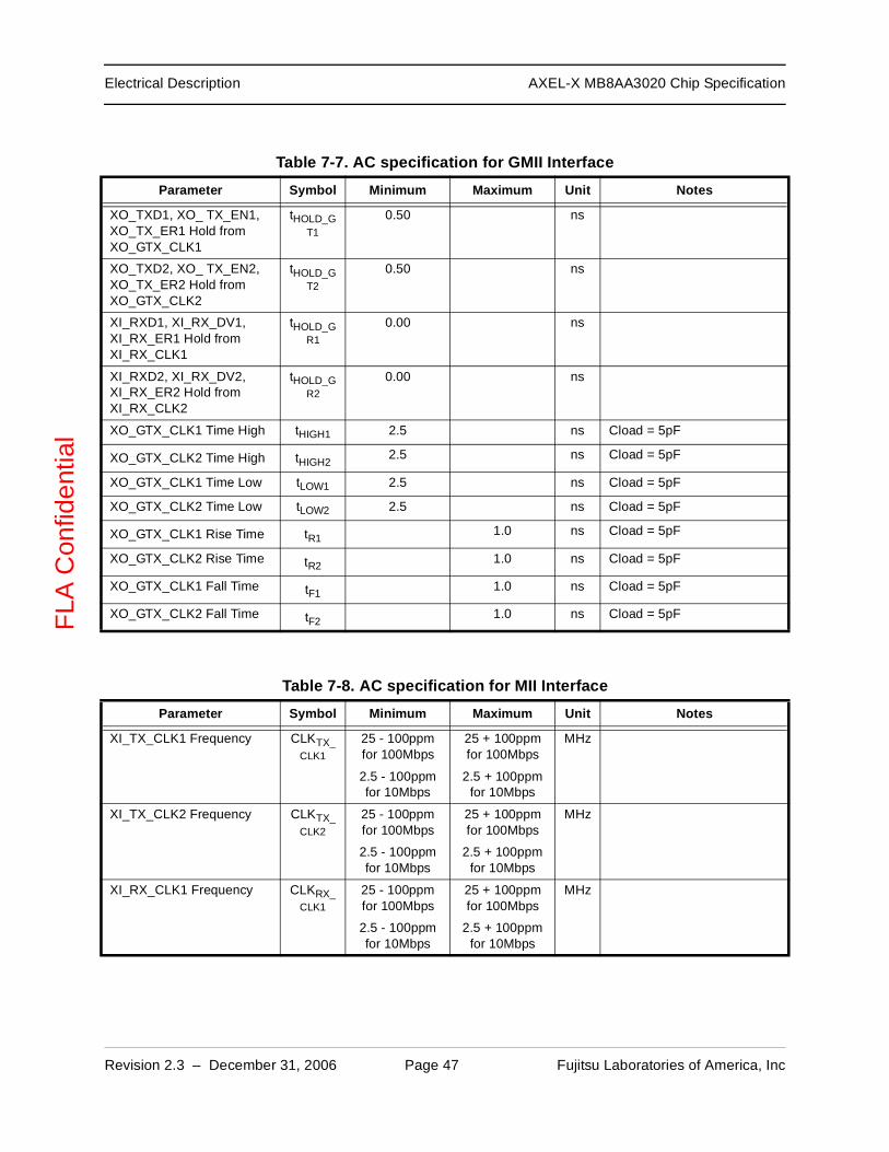
Table 7-7. AC specification for GMII Interface
Parameter Symbol Minimum Maximum Unit Notes
XO_GTX_CLK1 Frequency CLKGTX_CLK1
125 - 100ppm 125 + 100ppm MHz
XO_GTX_CLK2 Frequency CLKGTX_CLK2
125 - 100ppm 125 + 100ppm MHz
XI_RX_CLK1 Frequency CLKGRX_CLK1
125 - 100ppm 125 + 100ppm MHz
XI_RX_CLK2 Frequency CLKGRX_CLK2
125 - 100ppm 125 + 100ppm MHz
XO_TXD1, XO_ TX_EN1, XO_TX_ER1 Setup to XO_GTX_CLK1
tSETUP_GT1
2.50 ns
XO_TXD2, XO_ TX_EN2, XO_TX_ER2 Setup to XO_GTX_CLK2
tSETUP_GT2
2.50 ns
XI_RXD1, XI_RX_DV1, XI_RX_ER1 Setup to XI_RX_CLK1
tSETUP_GR1
2.00 ns
XI_RXD2, XI_RX_DV2, XI_RX_ER2 Setup to XI_RX_CLK2
tSETUP_GR2
2.00 ns
Table 7-5. AC specification
Parameter Symbol Minimum Typical Maximum Unit Notes
Revision 2.3 – December 31, 2006 Page 47 Fujitsu Laboratories of America, Inc
Electrical Description AXEL-X MB8AA3020 Chip SpecificationF
LA C
onfid
entia
l
XO_TXD1, XO_ TX_EN1, XO_TX_ER1 Hold from XO_GTX_CLK1
tHOLD_GT1
0.50 ns
XO_TXD2, XO_ TX_EN2, XO_TX_ER2 Hold from XO_GTX_CLK2
tHOLD_GT2
0.50 ns
XI_RXD1, XI_RX_DV1, XI_RX_ER1 Hold from XI_RX_CLK1
tHOLD_GR1
0.00 ns
XI_RXD2, XI_RX_DV2, XI_RX_ER2 Hold from XI_RX_CLK2
tHOLD_GR2
0.00 ns
XO_GTX_CLK1 Time High tHIGH1 2.5 ns Cload = 5pF
XO_GTX_CLK2 Time High tHIGH22.5 ns Cload = 5pF
XO_GTX_CLK1 Time Low tLOW1 2.5 ns Cload = 5pF
XO_GTX_CLK2 Time Low tLOW2 2.5 ns Cload = 5pF
XO_GTX_CLK1 Rise Time tR11.0 ns Cload = 5pF
XO_GTX_CLK2 Rise Time tR21.0 ns Cload = 5pF
XO_GTX_CLK1 Fall Time tF11.0 ns Cload = 5pF
XO_GTX_CLK2 Fall Time tF21.0 ns Cload = 5pF
Table 7-8. AC specification for MII Interface
Parameter Symbol Minimum Maximum Unit Notes
XI_TX_CLK1 Frequency CLKTX_CLK1
25 - 100ppm for 100Mbps
2.5 - 100ppm for 10Mbps
25 + 100ppm for 100Mbps
2.5 + 100ppm for 10Mbps
MHz
XI_TX_CLK2 Frequency CLKTX_CLK2
25 - 100ppm for 100Mbps
2.5 - 100ppm for 10Mbps
25 + 100ppm for 100Mbps
2.5 + 100ppm for 10Mbps
MHz
XI_RX_CLK1 Frequency CLKRX_CLK1
25 - 100ppm for 100Mbps
2.5 - 100ppm for 10Mbps
25 + 100ppm for 100Mbps
2.5 + 100ppm for 10Mbps
MHz
Table 7-7. AC specification for GMII Interface
Parameter Symbol Minimum Maximum Unit Notes
Revision 2.3 – December 31, 2006 Page 48 Fujitsu Laboratories of America, Inc
Electrical Description AXEL-X MB8AA3020 Chip SpecificationF
LA C
onfid
entia
l
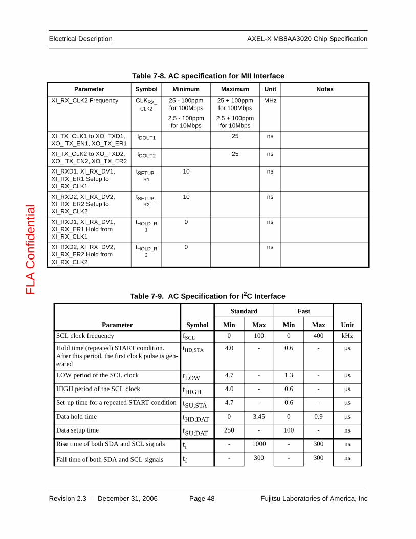
XI_RX_CLK2 Frequency CLKRX_CLK2
25 - 100ppm for 100Mbps
2.5 - 100ppm for 10Mbps
25 + 100ppm for 100Mbps
2.5 + 100ppm for 10Mbps
MHz
XI_TX_CLK1 to XO_TXD1, XO_ TX_EN1, XO_TX_ER1
tDOUT1 25 ns
XI_TX_CLK2 to XO_TXD2, XO_ TX_EN2, XO_TX_ER2
tDOUT2 25 ns
XI_RXD1, XI_RX_DV1, XI_RX_ER1 Setup to XI_RX_CLK1
tSETUP_R1
10 ns
XI_RXD2, XI_RX_DV2, XI_RX_ER2 Setup to XI_RX_CLK2
tSETUP_R2
10 ns
XI_RXD1, XI_RX_DV1, XI_RX_ER1 Hold from XI_RX_CLK1
tHOLD_R1
0 ns
XI_RXD2, XI_RX_DV2, XI_RX_ER2 Hold from XI_RX_CLK2
tHOLD_R2
0 ns
Table 7-9. AC Specification for I2C Interface
Parameter Symbol
Standard Fast
UnitMin Max Min Max
SCL clock frequency fSCL 0 100 0 400 kHz
Hold time (repeated) START condition. After this period, the first clock pulse is gen-erated
tHD;STA 4.0 - 0.6 - µs
LOW period of the SCL clock tLOW 4.7 - 1.3 - µs
HIGH period of the SCL clock tHIGH 4.0 - 0.6 - µs
Set-up time for a repeated START condition tSU;STA 4.7 - 0.6 - µs
Data hold time tHD;DAT 0 3.45 0 0.9 µs
Data setup time tSU;DAT 250 - 100 - ns
Rise time of both SDA and SCL signals tr - 1000 - 300 ns
Fall time of both SDA and SCL signals tf - 300 - 300 ns
Table 7-8. AC specification for MII Interface
Parameter Symbol Minimum Maximum Unit Notes
Revision 2.3 – December 31, 2006 Page 49 Fujitsu Laboratories of America, Inc
Electrical Description AXEL-X MB8AA3020 Chip SpecificationF
LA C
onfid
entia
l
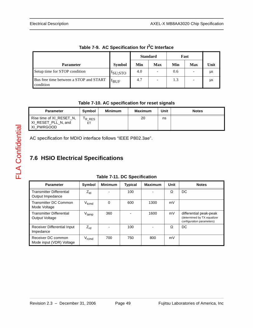
AC specification for MDIO interface follows “IEEE P802.3ae”.
7.6 HSIO Electrical Specifications
Setup time for STOP condition tSU;STO 4.0 - 0.6 - µs
Bus free time between a STOP and START condition
tBUF 4.7 - 1.3 - µs
Table 7-10. AC specification for reset signals
Parameter Symbol Minimum Maximum Unit Notes
Rise time of XI_RESET_N, XI_RESET_PLL_N, and XI_PWRGOOD
TR_RESET
20 ns
Table 7-11. DC Specification
Parameter Symbol Minimum Typical Maximum Unit Notes
Transmitter Differential Output Impedance
Ztd - 100 - Ω DC
Transmitter DC Common Mode Voltage
Vtcmd 0 600 1300 mV
Transmitter Differential Output Voltage
Vtamp 360 - 1600 mV differential peak-peak(determined by TX equalizer configuration parameters)
Receiver Differential Input Impedance
Zrd - 100 - Ω DC
Receiver DC common Mode input (VDR) Voltage
Vrcmd 700 750 800 mV
Table 7-9. AC Specification for I2C Interface
Parameter Symbol
Standard Fast
UnitMin Max Min Max

Revision 2.3 – December 31, 2006 Page 50 Fujitsu Laboratories of America, Inc
Electrical Description AXEL-X MB8AA3020 Chip SpecificationF
LA C
onfid
entia
l
Table 7-12. AC Specification
Parameter Symbol Minimum Typical Maximum Unit Notes
Transmitter Output Data Rate Ftd 10.3125-100 ppm
10.3125 10.3125+100 ppm
Gbps 10G serial mode
3.125-100 ppm
3.125 3.125+100 ppm
CX-4 mode
Transmitter Output Rise/Fall Time
Ttrf 24 - - ps 20% - 80%(depends on the TX equal-izer configuration parame-ters)
Transmitter Differential peak-to-peak output voltage differ-ence
Vtdppd - - 150 mV lane-to-lane differ-ence in CX-4 mode
Transmitter Differential Out-put Return Loss
SDD11 10 - - dB 0.1-0.625 GHz
A - - dB 0.625-3.943 GHz,A=10-10*Log10(F/0.625)
2 - - dB 3.943-10 GHz
Transmitter Output Total Jitter Ttj - - 0.3 UI 1UI=97.0ps, peak to peak
Receiver Data Rate Frd 10.3125-100 ppm
10.3125 10.3125+100 ppm
Gbps 10G serial mode
3.125-100 ppm
3.125 3.125+100 ppm
CX-4 mode
Receiver Differential Input Return Loss
SDD11 9 - - dB 0.1-2 GHz
A - - dB 2-7.5 GHz,A=9-12.2*Log10(F/2)
Receiver Common mode Input Return Loss
SCC11 6 - - dB 0.1-2.5 GHz
Receiver Jitter Tolerance JT 0.65 - - UI
Receiver CDR Lock Up Time Trlock - - 60 µs
XFP Clock Output Frequency Fck - 10.3125/64
- GHz Frequency is exactly equal to the Baudrate/64.
XFP Clock Output Differential Amplitude
Vcamp 640 - 1600 mVpp
XFP Clock Duty Cycle Duty 40 50 60 %
XFP Clock Output Rise/Fall Time
Tckrf 200 - 1250 ps 20% - 80%
XFP Clock RMS Random Jit-ter
Sigma - - 10 ps Up to 100MHz

Revision 2.3 – December 31, 2006 Page 51 Fujitsu Laboratories of America, Inc
Electrical Description AXEL-X MB8AA3020 Chip SpecificationF
LA C
onfid
entia
l
7.7 Power Dissipation
7.8 Reset Sequence
The reset sequence is defined for the following external pins.
• XI_RESET_N
• XI_RESET_PLL_N
• XI_PWRGOOD
Table 7-13. Power Dissipation
Parameter Symbol Min
Typical
Max Unit NotesXFIa
a. power consumption when all 10G ports are 10G serial.
XAUIb
b. power consumption when all 10G ports are XAUI.
Power Dissipation PD 18.6 18.0 W Total power dissipation
1.2V for core PVDD 7.3 W
2.5V for I/O PVDE 0.1 W
1.2V for HSIO SerDes PVDN 11.1 10.5 W XFI: Tx: default, Rx: 32/63c
XAUI: Tx: default, RX: bypass
c. DC gain is 32, and 1st gain is 64.
2.5V for HSIO SerDes PVDP 0.1 0.1 W

Revision 2.3 – December 31, 2006 Page 52 Fujitsu Laboratories of America, Inc
Electrical Description AXEL-X MB8AA3020 Chip SpecificationF
LA C
onfid
entia
l
Figure 7-1 shows the reset sequence using these external pins and Table 7-14 shows AC speci-fication for the reset sequence.
Figure 7-1. Reset Sequence
Table 7-14. Reset Sequence
Parameter Min. Value Max. Value Description
Tpg 0 µs N/A >= 0 µs
Tpll_res 25 µs N/A PLL reset time.
Tm_res 200 µs N/A Master reset time.
VDD, VDE, VDN, VDP, AVD
XI_PWRGOOD
XI_RESET_PLL_N
XI_RESET_N
external clocks and power must be stable
Tpg Tpll_res Tm_res
XI_Pmm_REFCLKP
XI_Pmm_REFCLKN