automotive lcd tv signal processor ic - panasonic ics for tv publication date: june 2006 sdb00081ceb...
TRANSCRIPT

1
ICs for TV
Publication date: June 2006 SDB00081CEB
AN2546FH-AAutomotive LCD TV signal processor IC
OverviewThe AN2546FH-A is a video signal processing IC built-in a 5-volt power-supply source driver for TFT color LCD
(normally white type), and it supports the NTSC, PAL and PAL-M/PAL-N systems. The main circuitry of this ICincludes video-signal processing circuit, color signal processing circuit, interface circuit, synchronizing circuit andmany color quality adjusting circuits. This IC converts the composite video signal or separated Y/C signal or RGBsignals into RGB signals available for TFT color LCD.
Features• Supply voltage: 3 V/5 V/7.5 V• Built-in a 5-volt power-supply source driver for TFT type LCD• Low consumption power (typ. 200 mW)• Supporting the NTSC, PAL, PAL-M and PAL-N systems• Supporting composite, component and color differential signal input• Video signal, analog RGB (2 systems)
One is for OSD (analog/digital).• Each mode setting is possible with I2C Bus control.• Electronic volume (D/A converter) built in• Contrast/Brightness/γ correction circuit built in• Horizontal and vertical display position adjustment are possible by serial control.• Improvement of weak electric field characteristics (Compared to AN2526FH/AN2526NFH: −5 dB)• At reverse stop, built-in output gain down function
Applications• 4 inches to 7 inches middle size TFT LCD equipment of normally white, of such as an in-car TV and an LCD
monitor for car navigation system.
Package• QFP064-P-1010AMain
tenan
ce/
Discon
tinued
Mainten
ance/D
iscont
inued
includ
es foll
owing
four P
roduct
lifecyc
le stag
e.
(planed
mainten
ance ty
pe, main
tenanc
e type,
planed
discon
tinued
typed,
discon
tinued
type)

AN2546FH-A
SDB00081CEB2
Application Circuit Examples1. Composite signal input
49 50 51 52 53 54 55 56 57 58 59 60 61 62 63 64PA
L o
rPA
L-M
PAL
-N
SDA
TASC
LC
KG
ND
2N
AV
Isy
nc.
VC
C1
(5.0
V)
VSS
POL
VD
DN
RG
B
L-d
et.
Sync
. in
R-Y ou
t
NT
SC
APC
det
.AC
C d
et.
Y-d
et.
Y-i
n
C-i
n
Kill
det
.
GN
D3
VC
C1
(5.0
V)
SC o
ut5.1
kΩ
2 kΩ
330
kΩ1
kΩ
15 k
Ω
68 k
Ω33
0 Ω
Com
posi
te s
igna
l
1 µF
15 µ
F
0.02
µF
0.1
µF
33
34
35
36
37
38
39
40
41
42
43
44
45
46
47
48
32 31 30 29 28V
CO
M
27 26 25 24 23 22 21 20 19 18 17
16
15
14
13
12
11
10
9
8
7
6
5
4
3
2
1
VC
C1
(5.0
V)
VR
EF
PWM
Log
icL
ogic
Log
icL
ogic Cla
mp
Del
ay
Shar
pnes
s
APC
Tin
t
Kill
erV
XO
gene
.
VX
O
BPFSy
nc.
cut
SW
AC
Cde
t.A
CC
amp.
YU
VSW
GC
A
Bri
ght
Reg
.
R-Y
, B-Y
DE
MO
D
DA
C
DA
C
Reg
.
I2C
Bus
VC
O1/
nSy
nc. s
epa.
HH
KIL
LV
SYN
Cdr
op
Ver
t.co
untPh
ase
com
p.f
det.
GC
A
B-Y ou
tB
-Y inR
-Y in
G-Y
gene
.M
atri
x
Int./
Ext
.SW
Cla
mp.
OSD SW
Con
tras
t
Gam
ma
Inve
rtL
imit
0.1
µF
0.1
µF
4.7
µF
NT
SC =
39
pFPA
L =
27
pF
47 µ
HPON
R
CO
M D
C
SEC
AM
bla
ckle
vel a
dj.2.2
µF
33 k
Ω10
µF
4.7
µF1
500
pF
VC
C1
VC
C3
15 µ
F
47 µ
H
Be
sure
to a
ttach
a p
ower
sup
ply
filte
rto
a p
ower
sup
ply
pin.
Pow
er s
uppl
y pi
n
Rec
omm
ende
d cr
ysta
l osc
illat
orN
TSC
: VSX
0160
(KIN
SEK
I, L
imite
d)PA
L: V
SX01
62(K
INSE
KI,
Lim
ited)
1 µF
YS
BL
AK
B-o
utB-o
utde
t.
R-d
et.1
µF G-d
et.1
µF B-d
et.
2.2
µF
R-i
n1G
-in1
B-i
n1R
-in2
G-i
n2B
-in2
G-o
ut
VC
OM
PWM
VD
HD
SCP R-o
ut G-o
utde
t.
GN
D1
2.2
µF
R-o
utde
t.2.
2 µF
VC
C2
(7.5
V)
VC
C3
(3.0
V)
0.01
µF
0.02
µF
15 µ
F
0.02
2 µF
0.47
µF
82 k
Ω
C-s
ync.
AFC
det.
50 k
Ω1
MΩ
3.3
kΩ10
kΩ
100
kΩ68
0 pF
•C
cou
plin
g in
put i
n an
ana
log
OSD
mod
e.•
Con
nect
to G
ND
in c
ase
of n
o us
ein
a d
igita
l OSD
mod
e.
Mainten
ance/
Discon
tinued
Mainten
ance/D
iscont
inued
includ
es foll
owing
four P
roduct
lifecyc
le stag
e.
(planed
mainten
ance ty
pe, main
tenanc
e type,
planed
discon
tinued
typed,
discon
tinued
type)

AN2546FH-A
3SDB00081CEB
Application Circuit Examples (continued)2. Component signal input
49 50 51 52 53 54 55 56 57 58 59 60 61 62 63 64PA
L o
rPA
L-M
PAL
-N
SDA
TASC
LC
KG
ND
2N
AV
Isy
nc.
VC
C1
(5.0
V)
VSS
POL
VD
DN
RG
B
L-d
et.
Sync
. in
R-Y ou
t
NT
SC
APC
det
.AC
C d
et.
Y-d
et.
Y-i
n
C-i
n
Kill
det
.
GN
D3
VC
C1
(5.0
V)
SC o
ut5.1
kΩ
330
kΩ1
kΩ
15 k
Ω
68 k
Ω33
0 Ω
Bri
ghtn
ess
and
sync
rono
us s
igna
l
1 µF
15 µ
F
0.02
µF
0.1
µF
33
34
35
36
37
38
39
40
41
42
43
44
45
46
47
48
32 31 30 29 28V
CO
M
27 26 25 24 23 22 21 20 19 18 17
16
15
14
13
12
11
10
9
8
7
6
5
4
3
2
1
VC
C1
(5.0
V)
VR
EF
PWM
Log
icL
ogic
Log
icL
ogic Cla
mp
Del
ay
Shar
pnes
s
APC
Tin
t
Kill
erV
XO
gene
.
VX
O
BPFSy
nc.
cut
SW
AC
Cde
t.A
CC
amp.
YU
VSW
GC
A
Bri
ght
Reg
.
R-Y
, B-Y
DE
MO
D
DA
C
DA
C
Reg
.
I2C
Bus
VC
O1/
nSy
nc. s
epa.
HH
KIL
LV
SYN
Cdr
op
Ver
t.co
untPh
ase
com
p.f
det.
GC
A
B-Y ou
tB
-Y inR
-Y in
G-Y
gene
.M
atri
x
Int./
Ext
.SW
Cla
mp.
OSD SW
Con
tras
t
Gam
ma
Inve
rtL
imit
0.1
µF
0.1
µF
4.7
µF
PON
R
CO
M D
C
SEC
AM
bla
ckle
vel a
dj.2.2
µF
33 k
Ω10
µF
4.7
µF1
500
pF
VC
C1
VC
C3
1 µF
YS
BL
AK
B-o
utB-o
utde
t.
R-d
et.1
µF G-d
et.1
µF B-d
et.
2.2
µF
R-i
n1G
-in1
B-i
n1R
-in2
G-i
n2B
-in2
G-o
ut
VC
OM
PWM
VD
HD
SCP R-o
ut G-o
utde
t.
GN
D1
2.2
µF
R-o
utde
t.2.
2 µF
VC
C2
(7.5
V)
VC
C3
(3.0
V)
0.01
µF
0.02
µF
15 µ
F
0.02
2 µF
0.47
µF
82 k
Ω
C-s
ync.
AFC
det.
50 k
Ω1
MΩ
3.3
kΩ10
kΩ
100
kΩ68
0 pF
15 µ
F
47 µ
H
Pow
er s
uppl
y pi
n•
C c
oupl
ing
inpu
t in
an a
nalo
g O
SD m
ode.
•C
onne
ct to
GN
D in
cas
e of
no
use
in a
dig
ital O
SD m
ode.
Be
sure
to a
ttach
a p
ower
sup
ply
filte
rto
a p
ower
sup
ply
pin.
Rec
omm
ende
d cr
ysta
l osc
illat
orN
TSC
: VSX
0160
(KIN
SEK
I, L
imite
d)PA
L: V
SX01
62(K
INSE
KI,
Lim
ited)
Mainten
ance/
Discon
tinued
Mainten
ance/D
iscont
inued
includ
es foll
owing
four P
roduct
lifecyc
le stag
e.
(planed
mainten
ance ty
pe, main
tenanc
e type,
planed
discon
tinued
typed,
discon
tinued
type)

AN2546FH-A
SDB00081CEB4
Application Circuit Examples (continued)3. Analog RGB signal input
49 50 51 52 53 54 55 56 57 58 59 60 61 62 63 64PA
L o
rPA
L-M
PAL
-N
SDA
TASC
LC
KG
ND
2N
AV
Isy
nc.
VC
C1
(5.0
V)
VSS
POL
VD
DN
RG
B
L-d
et.
Sync
. in
NT
SCGN
D3
VC
C1
(5.0
V)
330
kΩ1
kΩ
15 k
Ω
68 k
Ω33
0 Ω
Sync
hron
ous
sign
al
15 µ
F
33
34
35
36
37
38
39
40
41
42
43
44
45
46
47
48
32 31 30 29 28V
CO
M
27 26 25 24 23 22 21 20 19 18 17
16
15
14
13
12
11
10
9
8
7
6
5
4
3
2
1
VC
C1
(5.0
V)
VR
EF
PWM
Log
icL
ogic
Log
icL
ogic Cla
mp
Del
ay
Shar
pnes
s
APC
Tin
t
Kill
erV
XO
gene
.
VX
O
BPFSy
nc.
cut
SW
AC
Cde
t.A
CC
amp.
YU
VSW
GC
A
Bri
ght
Reg
.
R-Y
, B-Y
DE
MO
D
DA
C
DA
C
Reg
.
I2C
Bus
VC
O1/
nSy
nc. s
epa.
HH
KIL
LV
SYN
Cdr
op
Ver
t.co
untPh
ase
com
p.f
det.
GC
A
G-Y
gene
.M
atri
x
Int./
Ext
.SW
Cla
mp.
OSD SW
Con
tras
t
Gam
ma
Inve
rtL
imit
PON
R
CO
M D
C
SEC
AM
bla
ckle
vel a
dj.2.2
µF
33 k
Ω10
µF
4.7
µF1
500
pF
VC
C1
VC
C1
Req
uire
d on
ly w
hen
not u
sing
cry
stal
osc
illat
ors.
VC
C3
4.7
µF4.
7 µF
4.7
µF1
µF
YS
BL
AK
B-o
utB-o
utde
t.
R-d
et.1
µF G-d
et.1
µF B-d
et.
2.2
µF
R-i
n1G
-in1
B-i
n1R
-in2
G-i
n2B
-in2
G-o
ut
VC
OM
PWM
VD
HD
SCP R-o
ut G-o
utde
t.
GN
D1
2.2
µF
R-o
utde
t.2.
2 µF
VC
C2
(7.5
V)
VC
C3
(3.0
V)
0.01
µF
0.02
µF
15 µ
F
0.02
2 µF
0.47
µF
82 k
Ω
C-s
ync.
AFC
det.
50 k
Ω1
MΩ
3.3
kΩ
510
kΩ
510
kΩ
10 k
Ω
100
kΩ68
0 pF
Poss
ible
to c
hang
e th
e sy
nchr
onou
s si
gnal
inpu
t pin
acc
ordi
ng to
the
chan
nnel
10
valu
e.Po
ssib
le to
inpu
t to
pin
45 b
y 3
V[p
-p]
posi
tive
pola
rity
pul
se.
15 µ
F
47 µ
H
Pow
er s
uppl
y pi
n
App
ly a
hal
f VC
C1
volta
geto
pin
42
acco
rdin
g to
resi
stan
ce d
ivis
ion
whe
n no
tco
nnec
ting
crys
tal o
scill
ator
s.
•C
cou
plin
g in
put i
n an
ana
log
OSD
mod
e.•
Con
nect
to G
ND
in c
ase
of n
o us
ein
a d
igita
l OSD
mod
e.
Be
sure
to a
ttach
a p
ower
sup
ply
filte
rto
a p
ower
sup
ply
pin.
Rec
omm
ende
d cr
ysta
l osc
illat
orN
TSC
: VSX
0160
(KIN
SEK
I, L
imite
d)PA
L: V
SX01
62(K
INSE
KI,
Lim
ited)
Mainten
ance/
Discon
tinued
Mainten
ance/D
iscont
inued
includ
es foll
owing
four P
roduct
lifecyc
le stag
e.
(planed
mainten
ance ty
pe, main
tenanc
e type,
planed
discon
tinued
typed,
discon
tinued
type)
AN2546FH-A
5SDB00081CEB
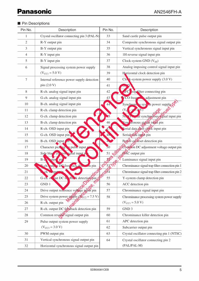
Pin Descriptions
Pin No. Description
1 Crystal oscillator connecting pin 3 (PAL-N)
2 R-Y output pin
3 B-Y output pin
4 R-Y input pin
5 B-Y input pin
6 Signal processing system power supply
(VCC1 = 5.0 V)
7 Internal reference power supply detection
pin (2.0 V)
8 R-ch. analog signal input pin
9 G-ch. analog signal input pin
10 B-ch. analog signal input pin
11 R-ch. clamp detection pin
12 G-ch. clamp detection pin
13 B-ch. clamp detection pin
14 R-ch. OSD input pin
15 G-ch. OSD input pin
16 B-ch. OSD input pin
17 Character picking up pulse input pin
18 Side black control signal input pin
19 B-ch. output pin
20 B-ch. output DC feedback detection pin
21 G-ch. output pin
22 G-ch. output DC feedback detection pin
23 GND 1
24 Drive output reference voltage input pin
25 Drive system power supply (VCC2 = 7.5 V)
26 R-ch. output pin
27 R-ch. output DC feedback detection pin
28 Common reverse signal output pin
29 Pulse output system power supply
(VCC3 = 3.0 V)
30 PWM output pin
31 Vertical synchronous signal output pin
32 Horizontal synchronous signal output pin
Pin No. Description
33 Sand castle pulse output pin
34 Composite synchronous signal output pin
35 Vertical synchronous signal input pin
36 1H reverse signal input pin
37 Clock-system GND (VSS)
38 Analog imposing control signal input pin
39 Horizontal clock detection pin
40 Clock-system power supply (3.0 V)
41 GND 2
42 AFC loop filter connecting pin
43 VCO frequency adjustment pin
44 Synchronous system power supply
(VCC1 = 5.0 V)
45 NAVI signal synchronous signal input pin
46 Synchronous signal input pin
47 Serial data shift clock input pin
48 Serial data input pin
49 Power-on reset detection pin
50 Common DC adjustment voltage output pin
51 DAC output pin
52 Luminance signal input pin
53 Chrominance signal trap filter connection pin 1
54 Chrominance signal trap filter connection pin 2
55 Y-system clamp detection pin
56 ACC detection pin
57 Chrominance signal input pin
58 Chrominance processing system power supply
(VCC1 = 5.0 V)
59 GND 3
60 Chrominance killer detection pin
61 APC detection pin
62 Subcarrier output pin
63 Crystal oscillator connecting pin 1 (NTSC)
64 Crystal oscillator connecting pin 2
(PAL/PAL-M)
Mainten
ance/
Discon
tinued
Mainten
ance/D
iscont
inued
includ
es foll
owing
four P
roduct
lifecyc
le stag
e.
(planed
mainten
ance ty
pe, main
tenanc
e type,
planed
discon
tinued
typed,
discon
tinued
type)

AN2546FH-A
SDB00081CEB6
Recommended Operating Range
Absolute Maximum Ratings
Parameter Symbol Rating Unit
Supply voltage VCC1 5.5 V
VCC2 8.5
VCC3 5.2
Supply current ICC mA
Power dissipation *2 PD 423 mW
Operating ambient temperature *1 Topr −30 to +85 °C
Storage temperature *1 Tstg −55 to +150 °C
Note) *1: Except for the operating ambient temperature and storage temperature, all ratings are for Ta = 25°C.
*2: The power dissipation shown is the value in free air for Topr = 85°C.
Parameter Symbol Range Unit
Supply voltage VCC1 4.7 to 5.3 V
VCC2 7.0 to 8.0
VCC3 2.7 to 3.3
Parameter Symbol Conditions Min Typ Max Unit
DC
VCC1-system current consumption ITOTAL1 Refer to product standards 32 44 mA
VCC2-system current consumption ITOTAL2 Refer to product standards 1.0 9.0 mA
VCC3-system current consumption ITOTAL3 Refer to product standards 2.0 mA
Chrominance system
R-Y standard gain GRY Refer to product standards 9.0 15 dB
R-Y/G-Y relative gain GRYGY Refer to product standards −5.0 −1.0 dB
B-Y standard gain GBY Refer to product standards 9.0 15 dB
B-Y/G-Y relative gain GBYGY Refer to product standards −15 −9.0 dB
High-level APC pull-in APH Refer to product standards 500 540 Hz
Low-level APC pull-in APL Refer to product standards −540 −500 Hz
ACC output characteristic 1 GACC1 Refer to product standards −1.0 1.0 dB
ACC output characteristic 2 GACC2 Refer to product standards −1.0 1.0 dB
Chrominance killer characteristic 1 VKILL1 Refer to product standards 400 mV[p-p]
Chrominance killer characteristic 2 VKILL2 Refer to product standards 600 mV[p-p]
Subcarrier amplitude SCV Refer to product standards 400 mV[p-p]
Y-system
Sharpness control characteristic GSH Refer to product standards 1.0 dB
Sharpness frequency characteristic 1 fSH1 Refer to product standards 4.0 dB
R-ch. contrast adjustment range 1 CTRR1 Refer to product standards 1.5 dB
Electrical Characteristics at Ta = 25°C
Mainten
ance/
Discon
tinued
Mainten
ance/D
iscont
inued
includ
es foll
owing
four P
roduct
lifecyc
le stag
e.
(planed
mainten
ance ty
pe, main
tenanc
e type,
planed
discon
tinued
typed,
discon
tinued
type)

AN2546FH-A
7SDB00081CEB
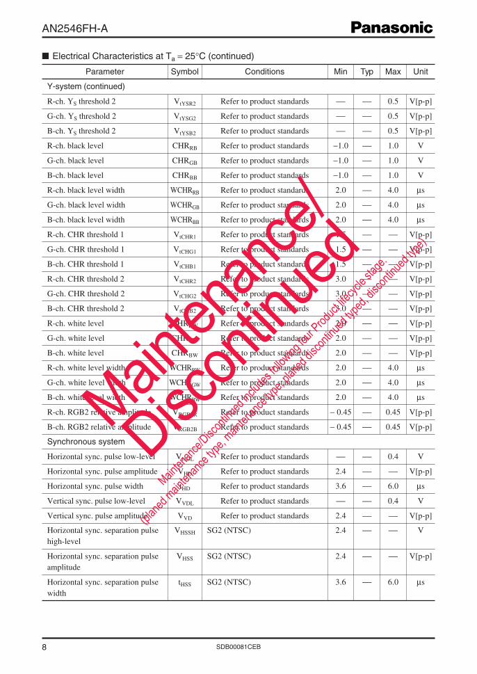
Electrical Characteristics at Ta = 25°C (continued)
Parameter Symbol Conditions Min Typ Max Unit
Y-system (continued)
G-ch. contrast adjustment range 1 CTRG1 Refer to product standards 1.5 dB
B-ch. contrast adjustment range 1 CTRB1 Refer to product standards 1.5 dB
R-ch. contrast adjustment range 2 CTRR2 Refer to product standards −2.5 dB
G-ch. contrast adjustment range 2 CTRG2 Refer to product standards −2.5 dB
B-ch. contrast adjustment range 2 CTRB2 Refer to product standards −2.5 dB
R-ch. pedestal amplitude minimum VPEDRmin Refer to product standards 2.0 V[p-p]
G-ch. pedestal amplitude minimum VPEDGmin Refer to product standards 2.0 V[p-p]
B-ch. pedestal amplitude minimum VPEDBmin Refer to product standards 2.0 V[p-p]
R-ch. pedestal amplitude maximum VPEDRmax Refer to product standards 3.0 V[p-p]
G-ch. pedestal amplitude maximum VPEDGmax Refer to product standards 3.0 V[p-p]
B-ch. pedestal amplitude maximum VPEDBmax Refer to product standards 3.0 V[p-p]
G-ch. output DC voltage VGDC Refer to product standards 2.35 2.85 V[p-p]
R-ch. gamma characteristic 1 GGAMR1 Refer to product standards −9.0 −3.0 dB
G-ch. gamma characteristic 1 GGAMG1 Refer to product standards −9.0 −3.0 dB
B-ch. gamma characteristic 1 GGAMB1 Refer to product standards −9.0 −3.0 dB
R-ch. gamma characteristic 2 GGAMR2 Refer to product standards −8.0 dB
G-ch. gamma characteristic 2 GGAMG2 Refer to product standards −8.0 dB
B-ch. gamma characteristic 2 GGAMB2 Refer to product standards −8.0 dB
R-ch. gamma characteristic 3 GGAMR3 Refer to product standards −5.0 0 dB
G-ch. gamma characteristic 3 GGAMG3 Refer to product standards −5.0 0 dB
B-ch. gamma characteristic 3 GGAMB3 Refer to product standards −5.0 0 dB
R-ch. white limiter high-level VWRRH Refer to product standards 3.0 V[p-p]
G-ch. white limiter high-level VWRGH Refer to product standards 3.0 V[p-p]
B-ch. white limiter high-level VWRBH Refer to product standards 3.0 V[p-p]
R-ch. white limiter low-level VWRRL Refer to product standards 3.2 V[p-p]
G-ch. white limiter low-level VWRGL Refer to product standards 3.2 V[p-p]
B-ch. white limiter low-level VWRBL Refer to product standards 3.2 V[p-p]
R-ch. black limiter low-level VBRRL Refer to product standards 3.0 V
G-ch. black limiter low-level VBRGL Refer to product standards 3.0 V
B-ch. black limiter low-level VBRBL Refer to product standards 3.0 V
R-ch. black limiter high-level VBRRH Refer to product standards 2.7 V
G-ch. black limiter high-level VBRGH Refer to product standards 2.7 V
B-ch. black limiter high-level VBRBH Refer to product standards 2.7 V
R-ch. YS threshold 1 VtYSR1 Refer to product standards 0.8 V[p-p]
G-ch. YS threshold 1 VtYSG1 Refer to product standards 0.8 V[p-p]
B-ch. YS threshold 1 VtYSB1 Refer to product standards 0.8 V[p-p]
Mainten
ance/
Discon
tinued
Mainten
ance/D
iscont
inued
includ
es foll
owing
four P
roduct
lifecyc
le stag
e.
(planed
mainten
ance ty
pe, main
tenanc
e type,
planed
discon
tinued
typed,
discon
tinued
type)
AN2546FH-A
SDB00081CEB8
Electrical Characteristics at Ta = 25°C (continued)
Parameter Symbol Conditions Min Typ Max Unit
Y-system (continued)
R-ch. YS threshold 2 VtYSR2 Refer to product standards 0.5 V[p-p]
G-ch. YS threshold 2 VtYSG2 Refer to product standards 0.5 V[p-p]
B-ch. YS threshold 2 VtYSB2 Refer to product standards 0.5 V[p-p]
R-ch. black level CHRRB Refer to product standards −1.0 1.0 V
G-ch. black level CHRGB Refer to product standards −1.0 1.0 V
B-ch. black level CHRBB Refer to product standards −1.0 1.0 V
R-ch. black level width WCHRRB Refer to product standards 2.0 4.0 µs
G-ch. black level width WCHRGB Refer to product standards 2.0 4.0 µs
B-ch. black level width WCHRBB Refer to product standards 2.0 4.0 µs
R-ch. CHR threshold 1 VtCHR1 Refer to product standards 1.5 V[p-p]
G-ch. CHR threshold 1 VtCHG1 Refer to product standards 1.5 V[p-p]
B-ch. CHR threshold 1 VtCHB1 Refer to product standards 1.5 V[p-p]
R-ch. CHR threshold 2 VtCHR2 Refer to product standards 3.0 V[p-p]
G-ch. CHR threshold 2 VtCHG2 Refer to product standards 3.0 V[p-p]
B-ch. CHR threshold 2 VtCHB2 Refer to product standards 3.0 V[p-p]
R-ch. white level CHRRW Refer to product standards 2.0 V[p-p]
G-ch. white level CHRGW Refer to product standards 2.0 V[p-p]
B-ch. white level CHRBW Refer to product standards 2.0 V[p-p]
R-ch. white level width WCHRRW Refer to product standards 2.0 4.0 µs
G-ch. white level width WCHRGW Refer to product standards 2.0 4.0 µs
B-ch. white level width WCHRBW Refer to product standards 2.0 4.0 µs
R-ch. RGB2 relative amplitude VRGB2R Refer to product standards − 0.45 0.45 V[p-p]
B-ch. RGB2 relative amplitude VRGB2B Refer to product standards − 0.45 0.45 V[p-p]
Synchronous system
Horizontal sync. pulse low-level VHDL Refer to product standards 0.4 V
Horizontal sync. pulse amplitude VHD Refer to product standards 2.4 V[p-p]
Horizontal sync. pulse width tHD Refer to product standards 3.6 6.0 µs
Vertical sync. pulse low-level VVDL Refer to product standards 0.4 V
Vertical sync. pulse amplitude VVD Refer to product standards 2.4 V[p-p]
Horizontal sync. separation pulse VHSSH SG2 (NTSC) 2.4 Vhigh-level
Horizontal sync. separation pulse VHSS SG2 (NTSC) 2.4 V[p-p]amplitude
Horizontal sync. separation pulse tHSS SG2 (NTSC) 3.6 6.0 µswidth
Mainten
ance/
Discon
tinued
Mainten
ance/D
iscont
inued
includ
es foll
owing
four P
roduct
lifecyc
le stag
e.
(planed
mainten
ance ty
pe, main
tenanc
e type,
planed
discon
tinued
typed,
discon
tinued
type)

AN2546FH-A
9SDB00081CEB
Terminal Equivalent Circuits
Pin No. Equivalent circuit Description Voltage · Waveform
1 VXO3: PAL-N crystal oscillator con-
necting pin
Use the capacitor with tem-
perature characteristics
(N750) to connect to the
crystal oscillator.
2 R-Y out: R-Y signalOutput pin of R-Y signal de-
modulated from video signal
3 B-Y out: B-Y signalOutput pin of B-Y signal de-
modulated from video signal
4 R-Y in: R-Y signalR-Y signal input pin in a color
difference mode and in the
standard PAL
1
Pin 58VCC1
Pin 59GND
190 Ω
1 kΩ
2
Pin 58VCC1
Pin 59GND
2 kΩ
1H
3
Pin 58VCC1
Pin 59GND
2 kΩ
1H
4
Pin 58VCC1
Pin 59GND
Pin 7VREF
5 kΩ
5 kΩ 5 kΩ
17.5 kΩ
5 kΩ 5 kΩ
2 kΩ1H
Mainten
ance/
Discon
tinued
Mainten
ance/D
iscont
inued
includ
es foll
owing
four P
roduct
lifecyc
le stag
e.
(planed
mainten
ance ty
pe, main
tenanc
e type,
planed
discon
tinued
typed,
discon
tinued
type)

AN2546FH-A
SDB00081CEB10
Terminal Equivalent Circuits (continued)
Pin No. Equivalent circuit Description Voltage · Waveform
5 B-Y in: B-Y signalB-Y signal input pin in a color
difference mode and in the
standard PAL
6 VCC1: Drive block 5.0 V-system
power supply pin
7 VREF: Reference voltage output pin
2.0 V typ.
8 R-in 1: Analog R signalAnalog R signal input
9 G-in 1: Analog G signalAnalog G signal input
5
Pin 58VCC1
Pin 59GND
Pin 7VREF
5 kΩ
5 kΩ 5 kΩ
17.5 kΩ
5 kΩ 5 kΩ
2 kΩ
1H
60 ΩPin 6VCC1
Pin 23GND
200 Ω30 kΩ
26 kΩ
1 kΩ7
5 kΩ8
Pin 6VCC1
Pin 7VREF
Pin 23GND
0.7 V[p-p]typ.
5 kΩ9
Pin 6VCC1
Pin 7VREF
Pin 23GND
0.7 V[p-p]typ.
Mainten
ance/
Discon
tinued
Mainten
ance/D
iscont
inued
includ
es foll
owing
four P
roduct
lifecyc
le stag
e.
(planed
mainten
ance ty
pe, main
tenanc
e type,
planed
discon
tinued
typed,
discon
tinued
type)

AN2546FH-A
11SDB00081CEB
Pin No. Equivalent circuit Description Voltage · Waveform
10 B-in 1: Analog B signalAnalog B signal input
11 R-ch. det.: R-ch. clamping capacitor
coupling pin
12 G-ch. det.: G-ch. clamping capacitor
coupling pin
13 B-ch. det.: B-ch. clamping capacitor
coupling pin
Terminal Equivalent Circuits (continued)
5 kΩ10
Pin 6VCC1
Pin 7VREF
Pin 23GND
1 kΩ 1 kΩ
Pin 6VCC1
Pin 23GND
500 Ω11
HSS
0.7 V[p-p]typ.
1 kΩ 1 kΩ
Pin 6VCC1
Pin 23GND
500 Ω12
HSS
1 kΩ 1 kΩ
Pin 6VCC1
Pin 23GND
500 Ω13
HSS
Mainten
ance/
Discon
tinued
Mainten
ance/D
iscont
inued
includ
es foll
owing
four P
roduct
lifecyc
le stag
e.
(planed
mainten
ance ty
pe, main
tenanc
e type,
planed
discon
tinued
typed,
discon
tinued
type)

AN2546FH-A
SDB00081CEB12
Pin No. Equivalent circuit Description Voltage · Waveform
14 R-in 2: Analog OSDCharacter insertion signal in-
put for R-ch., supporting ana-
log and digital OSD
Digital OSD
15 G-in 2: Analog OSDCharacter insertion signal in-
put for G-ch., supporting
analog and digital OSD
Digital OSD
16 B-in 2: Analog OSDCharacter insertion signal in-
put for B-ch., supporting ana-
log and digital OSD
Digital OSD
17 YS:Character picking up signal
input
18 BLAK:Black level indication con-
trol signal input pin
Terminal Equivalent Circuits (continued)
5 kΩ14
Pin 6VCC1
Pin7VREF
Pin 23GND
DigitalOSD circuit
5 kΩ15
Pin 6VCC1
Pin7VREF
Pin 23GND
DigitalOSD circuit
5 kΩ16
Pin 6VCC1
Pin7VREF
Pin 23GND
DigitalOSD circuit
15 kΩ17
100 kΩ
Pin 23GND
10 kΩ
15 kΩ18
100 kΩ
Pin 23GND
10 kΩ
0.7 V[p-p]typ.
VDD
GND
0.7 V[p-p]typ.
VDD
GND
0.7 V[p-p]typ.
VDD
GND
VDD
GND
VDD
GND
Mainten
ance/
Discon
tinued
Mainten
ance/D
iscont
inued
includ
es foll
owing
four P
roduct
lifecyc
le stag
e.
(planed
mainten
ance ty
pe, main
tenanc
e type,
planed
discon
tinued
typed,
discon
tinued
type)

AN2546FH-A
13SDB00081CEB
Pin No. Equivalent circuit Description Voltage · Waveform
19 B-out:B signal output pin
20 B-ch. AVE det.: B-ch. output DC feedback
detection pin
21 G-out:G signal output pin
22 G-ch. AVE det.: G-ch. output DC feedback
detection pin
23 GND 1: Drive circuits system GND
Terminal Equivalent Circuits (continued)
19
100 ΩPin 25VCC2
Pin 6VCC1
Pin 23GND16 kΩ
2 kΩ
100 kΩ20
Pin 6VCC1
Pin 23GND
19
21
100 ΩPin 25VCC2
Pin 6VCC1
Pin 23GND16 kΩ
2 kΩ
100 kΩ22
Pin 6VCC1
Pin 23GND
21
Mainten
ance/
Discon
tinued
Mainten
ance/D
iscont
inued
includ
es foll
owing
four P
roduct
lifecyc
le stag
e.
(planed
mainten
ance ty
pe, main
tenanc
e type,
planed
discon
tinued
typed,
discon
tinued
type)

AN2546FH-A
SDB00081CEB14
Pin No. Equivalent circuit Description Voltage · Waveform
24 AVE : R,G,B output DC reference
voltage pin
25 VCC2: 7.5 V system power supply
26 R-out:R signal output pin
27 R-ch. AVE det.:R-ch. output DC feedback
detection pin
28 Common out:Voltage output pin for common.
Output impedance; Approx.
150 Ω
Terminal Equivalent Circuits (continued)
24
100 kΩ
Pin 6VCC1
Pin 23GND
8 kΩ
2 kΩ
100 kΩ
26
100 Ω
Pin 25VCC2
Pin 6VCC1
Pin 23GND16 kΩ
2 kΩ
100 kΩ27
Pin 6VCC1
Pin 23GND
26
ch.1
ch.128
Pin 25VCC2
Pin 23GND
100 kΩ
15 kΩ
200 Ω
Mainten
ance/
Discon
tinued
Mainten
ance/D
iscont
inued
includ
es foll
owing
four P
roduct
lifecyc
le stag
e.
(planed
mainten
ance ty
pe, main
tenanc
e type,
planed
discon
tinued
typed,
discon
tinued
type)

AN2546FH-A
15SDB00081CEB
Pin No. Equivalent circuit Description Voltage · Waveform
29 VCC3: Logic output circuits system
power supply 3.0 V typ.
30 PWM: Output waveformPWM signal output pin
31 VD: Output waveformVertical synchronous signal
output pin
32 HD: Output waveformHorizontal synchronous sig-
nal output pin
33 SCP out:Sand castle pulse output pin
34 HSS: Output waveformComposite synchronous sig-
nal output pin
Terminal Equivalent Circuits (continued)
30
Pin 29VCC3
Pin 23GND
Pin 37VSS
0 V
VCC3
31
Pin 29VCC3
Pin 23GND
Pin 37VSS
0 V
VCC3
32
Pin 29VCC3
Pin 23GND
Pin 37VSS
0 V
VCC3
33
100 Ω 100 Ω
41.3 kΩ
Pin 44VCC1
Pin 41GND
350 Ω
2.0 V[p-p]typ.
4.0 V[p-p]typ.
Burst time
Vertical/Horizontalblanking time
34
Pin 29VCC3
Pin 23GND
Pin 37VSS
0 V
VCC3
Mainten
ance/
Discon
tinued
Mainten
ance/D
iscont
inued
includ
es foll
owing
four P
roduct
lifecyc
le stag
e.
(planed
mainten
ance ty
pe, main
tenanc
e type,
planed
discon
tinued
typed,
discon
tinued
type)

AN2546FH-A
SDB00081CEB16
Pin No. Equivalent circuit Description Voltage · Waveform
35 VDB in: High or LowVertical synchronous pulse
input pin
36 Ext. pol.: High or Low1H reverse signal input pin
37 VSS : MOS system GND
38 PRGB: High or LowAnalog OSD signal input
Mode start-up signal input pin
Valid only in the analog OSD
mode
High = Analog OSD start up
39 LDET: Capacitor coupling pin for
the horizontal unlock detect-
ing circuit
40 VDD: Capacitor connection pin for
MOS part power supply
3.0 V typ.
41 GND 2: Pulse system GND
42 AFC det.:AFC filter connecting pin
Input impedance; 100 kΩ or
more
Terminal Equivalent Circuits (continued)
35
Pin 23GND
15 kΩ
100 kΩ10 kΩ
36
Pin 23GND
15 kΩ
100 kΩ10 kΩ
38
Pin 23GND
15 kΩ
100 kΩ10 kΩ
39
Pin 44VCC1
Pin 41GND
10 kΩ
12 kΩ
200 Ω
60 Ω
60 Ω
42
Pin 41GND
Pin 44VCC1
1 kΩ
1 kΩ
2 kΩ
2 kΩ
1H
Mainten
ance/
Discon
tinued
Mainten
ance/D
iscont
inued
includ
es foll
owing
four P
roduct
lifecyc
le stag
e.
(planed
mainten
ance ty
pe, main
tenanc
e type,
planed
discon
tinued
typed,
discon
tinued
type)

AN2546FH-A
17SDB00081CEB
Pin No. Equivalent circuit Description Voltage · Waveform
43 H fO: VCO oscillation frequency
adjusting resistor connection
pin
44 VCC1: Pulse system power supply
5.0 V
45 NAVI sync-in:Synchronous signal input pin
for the signal of car naviga-
tion system
Negative polarity input
46 HSS in: Input signal example:Sync. signal input pin Video signal
Separates a sync. signal from
luminance signal (video sig-
nal)
47 SCLK:Serial clock input pin
48 DAT:Serial data input pin
Terminal Equivalent Circuits (continued)
43
Pin 41GND
Pin 44VCC1
2 kΩ
5 pF10 kΩ10 kΩ
45
Pin 23GND
15 kΩ
100 kΩ10 kΩ
0 V
VDD
46
Pin 44VCC1
Pin 41GND
50 kΩ850 Ω
85 Ω
21.7 kΩ 32.5 kΩ
47
Pin 23GND
15 kΩ
100 kΩ10 kΩ
Pin 44VCC4
48
Pin 23GND
15 kΩ
100 kΩ10 kΩ
Mainten
ance/
Discon
tinued
Mainten
ance/D
iscont
inued
includ
es foll
owing
four P
roduct
lifecyc
le stag
e.
(planed
mainten
ance ty
pe, main
tenanc
e type,
planed
discon
tinued
typed,
discon
tinued
type)

AN2546FH-A
SDB00081CEB18
Pin No. Equivalent circuit Description Voltage · Waveform
49 RST: Capacitor coupling pin for
power-on reset
50 Com. DC: DCDC voltage output pin
51 DAC-out: DCDC voltage output pin
52 Y-in: Input signal example:Luminance signal input pin Video signal
Input luminance signal (video
signal)
53 Trap-out: Trap connecting pin
Trapping a chrominance sig-
nal by connecting external
inductor and capacitor. Not
necessary in case that an in-
put signal is a component.
Terminal Equivalent Circuits (continued)
49
Pin 44VCC1
Pin 37VSS
Pin 41GND
5 kΩ
500 Ω100 kΩ
50 kΩ
50
Pin 41GND
Pin 44VCC11.5 pF
36 kΩ
46 kΩ
40 kΩ
51
Pin 41GND
Pin 44VCC11.5 pF
36 kΩ
46 kΩ
40 kΩ
52
Pin 58VCC1
53
Pin 59GND
2 kΩ
2 kΩ
50 Ω
50 kΩ
Mainten
ance/
Discon
tinued
Mainten
ance/D
iscont
inued
includ
es foll
owing
four P
roduct
lifecyc
le stag
e.
(planed
mainten
ance ty
pe, main
tenanc
e type,
planed
discon
tinued
typed,
discon
tinued
type)

AN2546FH-A
19SDB00081CEB
Pin No. Equivalent circuit Description Voltage · Waveform
54 Trap-in: Trap connecting pin
The pair with pin 53
55 Y-det.: Capacitor coupling pin for
luminance signal clamping
56 ACC det.: ACC capacitor connecting
pin, adjusting the amplitude
of a burst signal automati-
cally
57 C-in: Input signal example:Chrominance signal input pin Video signal
Input chrominance signal
(video signal)
58 VCC1: Power supply 5.0 V typ.
Chrominance and luminance
signal processing system.
59 GND 3: GND for chrominance and lum-
inance signal processing system
Terminal Equivalent Circuits (continued)
54
Pin 58VCC1
Pin 59GND
2 kΩ
55
Pin 58VCC1
Pin 59GND
1 kΩ 1 kΩ
2 kΩ
56
Pin 59GND
Pin 58VCC1
1 kΩ
5 kΩ
1 kΩ
1 kΩ1 kΩ2 kΩ
5 kΩ
57
Pin 58VCC1
Pin 59GND
50 kΩ
Mainten
ance/
Discon
tinued
Mainten
ance/D
iscont
inued
includ
es foll
owing
four P
roduct
lifecyc
le stag
e.
(planed
mainten
ance ty
pe, main
tenanc
e type,
planed
discon
tinued
typed,
discon
tinued
type)

AN2546FH-A
SDB00081CEB20
Pin No. Equivalent circuit Description Voltage · Waveform
60 Kill det.: Killer capacitor coupling pin
To prevent degradation of
image in a small amplitude
of a burst signal, this pin
stops a chrominance signal
and the mode changes to
black and white mode.
61 APC det.: APC capacitor coupling pin
Matching the phase of a crys-
tal oscillation to that of burst
signal
62 SCP out: NTSC 3.58 MHzSubcarrier pulse output pin PAL 4.43 MHz
63 VXO1: NTSC crystal oscillator con-
necting pin
Use the capacitor with tem-
perature characteristics
(N750) to connect to the
crystal oscillator.
Terminal Equivalent Circuits (continued)
60
Pin 58VCC1
Pin 59GND
1.5 kΩ
72 kΩ
90 kΩ
61
Pin 58VCC1
Pin 59GND
2 kΩ 2 kΩ 1 kΩ
50 kΩ
100 kΩ
1 kΩ 1 kΩ 31 kΩ41 kΩ
45 kΩ
5 kΩ
5 kΩ
50 kΩ
62
Pin 58VCC1
Pin 59GND
10 kΩ
10 kΩ
63
Pin 58VCC1
Pin 59GND
190 Ω
1 kΩ
Mainten
ance/
Discon
tinued
Mainten
ance/D
iscont
inued
includ
es foll
owing
four P
roduct
lifecyc
le stag
e.
(planed
mainten
ance ty
pe, main
tenanc
e type,
planed
discon
tinued
typed,
discon
tinued
type)

AN2546FH-A
21SDB00081CEB
Pin No. Equivalent circuit Description Voltage · Waveform
64 VXO2: PAL and PAL-M crystal os-
cillator connecting pin
Use the capacitor with tem-
perature characteristics
(N750) to connect to the
crystal oscillator.
Terminal Equivalent Circuits (continued)
Usage Notes• The supply voltage applied to pin 6, pin 25, pin 29, pin 44, and pin 58 must be brought up at the same time.• The crystal oscillator used must be evaluated thoroughly, because chrominance signal processing system characteris-
tics change by the crystal oscillator type.• The conversion of the analog RGB signals and the analog OSD signals with synchronous signals is not supported.• Input the analog RGB signals and the analog OSD signals after filtering the pedestal parts of these signals.• Evaluated thoroughly on the application of this device in PAL.
Technical Data1. Serial interface description
1) I2C bus control modeA serial data is capable of transferring 9-bit unit of 8-bit transfer data and 1-bit answering data using two kinds
of signal lines of data and shift clock.When a slave address after setting a start condition matches the address on the IC side, you can receive the data
to be transmitted from then. Once the stop condition is set up, the next transmitting data will be ignored until thestart condition is set up.
There are two kinds of transfer mode: an auto-increment mode which does not transmit subaddress, and dataupgrade mode which transmits subaddress + data by 2 bytes.
The typical models of communication sequence are shown below:
(1) Start conditionWhen the S-data changes from high level to low level at SCLK = high level, a data receiving mode becomes
available.
(2) Slave address transferThe slave address of the AN2546FH-A is 88h.
64
Pin 58VCC1
Pin 59GND
190 Ω
1 kΩ
Subaddress transfer
Acknowledge bit
1
Pin 48S-data
Pin 47SCLK
2 3 4 5 6 7 8 9 1 2
Start condition
Mainten
ance/
Discon
tinued
Mainten
ance/D
iscont
inued
includ
es foll
owing
four P
roduct
lifecyc
le stag
e.
(planed
mainten
ance ty
pe, main
tenanc
e type,
planed
discon
tinued
typed,
discon
tinued
type)

AN2546FH-A
SDB00081CEB22
Technical Data (continued)1. Serial interface description (continued)
1) I2C bus control mode (continued)
(3) Subaddress transferWhen a data transfer mode bit is 0, all the serial data columns transferred until a stop condition is set is
regarded as the data block.
(5) Stop conditionWhen S-data changes from low level to high level at SCLK = high level, data reception is halted.
(6) Pulse timingTiming chart expanded diagram
(4) Data transfer
Data transferSlave address transferAcknowledge bit
1
D7 D6 D5 D4 D3 D2 D1 D0Pin 48S-data
Pin 47SCLK
2 3 4 5 6 7 8 98 9 1 2
Data transfer mode bit"1": Data update mode"0": Auto increment mode
Acknowledge bit
1
D7 D6 D5 D4 D3 D2 D1 D0Pin 48S-data
Pin 47SCLK
2 3 4 5 6 7 8 98 9 1 2
At auto increment mode: Data transferAt data update mode: Stop condition
Pin 48S-data
Pin 47SCLK
tf
tLOW
tBUF
tHDSTA tr tHIGH tSUDAT
tSUSTO
tHDDAT
Parameter Symbol Min Typ Max Unit
SCLK clock frequency tSCL 0 400 kHz
Bus free-time for stop condition and start condition tBUF 1.3 µs
Hold time start condition tHDSTA 0.6 µs
SCLK clock low-state hold time tLOW 1.3 µs
SCLK clock high-state hold time tHIGH 0.6 µs
Data hold time tHDDAT 0 µs
Data setup time tSUDAT 100 ns
S-data and SCLK signal rise time tr 300 ns
S-data and SCLK signal fall time tf 300 ns
Stop condition setup time tSUSTO 0.6 µs
Mainten
ance/
Discon
tinued
Mainten
ance/D
iscont
inued
includ
es foll
owing
four P
roduct
lifecyc
le stag
e.
(planed
mainten
ance ty
pe, main
tenanc
e type,
planed
discon
tinued
typed,
discon
tinued
type)

AN2546FH-A
23SDB00081CEB
Technical Data (continued)1. Serial interface description (continued)
2) Mode setting channel bits table
ch. Sub- Initial value D7 D6 D5 D4 D3 D2 D1 D0address (HEX)
1 01 80 Common amplitude
2 02 80 Luminance gain
3 03 80 Color gain
4 04 80 Hue
5 05 40 HGA Black limiter
6 06 80 Brightness
7 07 80 DBOSC Aperture
8 08 80 R-ch. sub-brightness
9 09 80 B-ch. sub-brightness
10 0A C0 DCLP White peak limiter
11 0B 80 Gamma 1
12 0C 80 Gamma 2
13 0D 80 Contrast
14 0E 80 R-ch. sub-contrast
15 0F 80 B-ch. sub-contrast
16 10 80 VCO free-run *1
17 11 03 DFVD DFSC DPALM DPALN DSECAM DVMODE DUV DCINT
18 12 00 MACRON PLL stop position adjustment Vertical position adjustment
19 13 80 HOSEI PWMT4 KOTEI Horizontal position adjustment
20 14 80 PWM frequency adjustment BLAK Burst cleaning pulse position adjustment
21 15 80 PWM duty
22 16 7F EXTTEST DHTS EXCHFI POLSW DMOSD DSC DCPS DQPAL
23 17 80 Common DC *2
24 18 80 DC output adjustment
Note) *1: VCO free-run adjustment; ch.23 = 02h or more, EXTTEST = High
*2: 00h, 01h are prohibition of use because of test mode.
Mainten
ance/
Discon
tinued
Mainten
ance/D
iscont
inued
includ
es foll
owing
four P
roduct
lifecyc
le stag
e.
(planed
mainten
ance ty
pe, main
tenanc
e type,
planed
discon
tinued
typed,
discon
tinued
type)
AN2546FH-A
SDB00081CEB24
Technical Data (continued)1. Serial interface description (continued)
2) Mode setting channel bits table (continued)
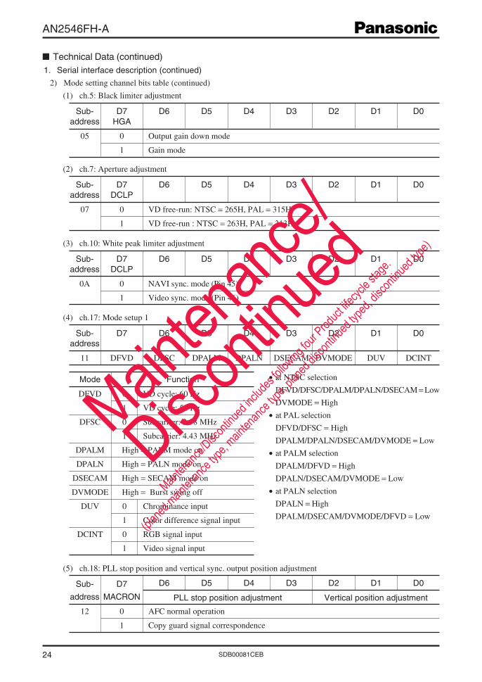
(1) ch.5: Black limiter adjustment
Sub- D7 D6 D5 D4 D3 D2 D1 D0address DCLP
0A 0 NAVI sync. mode (Pin 45)
1 Video sync. mode (Pin 46)
(4) ch.17: Mode setup 1
Sub- D7 D6 D5 D4 D3 D2 D1 D0address
11 DFVD DFSC DPALM DPALN DSECAM DVMODE DUV DCINT
Mode Function
DFVD 0 VD cycle: 60 Hz
1 VD cycle: 50 Hz
DFSC 0 Subcarrier: 3.58 MHz
1 Subcarrier: 4.43 MHz
DPALM High = PALM mode on
DPALN High = PALN mode on
DSECAM High = SECAM mode on
DVMODE High = Burst swing off
DUV 0 Chrominance input
1 Color difference signal input
DCINT 0 RGB signal input
1 Video signal input
• at NTSC selection
DFVD/DFSC/DPALM/DPALN/DSECAM = Low
DVMODE = High
• at PAL selection
DFVD/DFSC = High
DPALM/DPALN/DSECAM/DVMODE = Low
• at PALM selection
DPALM/DFVD = High
DPALN/DSECAM/DVMODE = Low
• at PALN selection
DPALN = High
DPALM/DSECAM/DVMODE/DFVD = Low
(5) ch.18: PLL stop position and vertical sync. output position adjustment
Sub- D7 D6 D5 D4 D3 D2 D1 D0
address MACRON PLL stop position adjustment Vertical position adjustment
12 0 AFC normal operation
1 Copy guard signal correspondence
(3) ch.10: White peak limiter adjustment
Sub- D7 D6 D5 D4 D3 D2 D1 D0address HGA
05 0 Output gain down mode
1 Gain mode
(2) ch.7: Aperture adjustment
Sub- D7 D6 D5 D4 D3 D2 D1 D0address DCLP
07 0 VD free-run: NTSC = 265H, PAL = 315H
1 VD free-run : NTSC = 263H, PAL = 313H
Mainten
ance/
Discon
tinued
Mainten
ance/D
iscont
inued
includ
es foll
owing
four P
roduct
lifecyc
le stag
e.
(planed
mainten
ance ty
pe, main
tenanc
e type,
planed
discon
tinued
typed,
discon
tinued
type)

AN2546FH-A
25SDB00081CEB
Technical Data (continued)1. Serial interface description (continued)
2) Mode setting channel bits table (continued)
(5) ch.18: PLL stop position and vertical sync. position adjustment (continued)
<Vertical synchronous output timing adjustment range>
Pin 35 input
Composite sync.signal odd numberfield
Pin 31 outputodd number fieldFIXHD = "0"
Pin 31 outputodd number fieldFIXHD = "1"
8H2H to 9H (D0 to D2)
3Η
Composite sync.signal even numberfield
Pin 31 outputEXCHF = "1"FIXHD = "0"
Pin 31 outputEXCHF = "1"FIXHD = "1"
Pin 31 outputEXCHF = "0"FIXHD = "0"
Pin31 outputEXCHF = "0"FIXHD = "1"
8H
8H
3Η
3Η
The above timing chart indicates (D2,D1,D0) = "101".For (D2,D1,D0) = "000", the pin 32 output width is 9H.
The pin 31 timing is synchronous with the pin 35 input timing. The above timing chart is just for reference
1.5H to 8.5H (D0 to D2)
2.5H to 9.5H (D0 to D2)
Pin 35 input
Composite sync.signal odd numberfield
Odd number field
EXCHF = "1"
EXCHF = "0"
Composite sync.signal even numberfield
6H to 9H (D3 to D4)
Horizontal PLL onHorizontal PLL off
0-line 1 2 3
5.5H to 8.5H (D3 to D4)
Horizontal PLL onHorizontal PLL off
6.5H to 9.5H (D3 to D4)
Horizontal PLL onHorizontal PLL off
The above timing chart indicates (D4,D3) = "01".PLL stop line number: 254-line (NTSC)
302-line (PAL)
<Horizontal PLL start position adjustment range>
Mainten
ance/
Discon
tinued
Mainten
ance/D
iscont
inued
includ
es foll
owing
four P
roduct
lifecyc
le stag
e.
(planed
mainten
ance ty
pe, main
tenanc
e type,
planed
discon
tinued
typed,
discon
tinued
type)
AN2546FH-A
SDB00081CEB26
Technical Data (continued)1. Serial interface description (continued)
2) Mode setting channel bits table (continued)
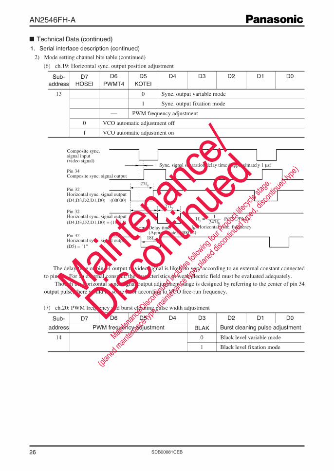
(6) ch.19: Horizontal sync. output position adjustment
Sub- D7 D6 D5 D4 D3 D2 D1 D0address HOSEI PWMT4 KOTEI
13 0 Sync. output variable mode
1 Sync. output fixation mode
PWM frequency adjustment
0 VCO automatic adjustment off
1 VCO automatic adjustment on
The delay time of pin 34 output to video signal is likely to vary according to an external constant connectedto pin 46. For an external constant, the characteristics in weak electric field must be evaluated adequately.
Though the horizontal sync. signal output adjustment range is designed by referring to the center of pin 34output pulse, there would be some error according to VCO free-run frequency.
(7) ch.20: PWM frequency and burst cleaning pulse width adjustment
Pin 34Composite sync. signal output
Pin 32Horizontal sync. signal output(D4,D3,D2,D1,D0) = (00000)
Composite sync.signal input(video signal)
Sync. signal separation delay time (Approximately 1 µs)
27fy
Pin 32Horizontal sync. signal output(D4,D3,D2,D1,D0) = (11111)
Pin 32Horizontal sync. signal output(D5) = "1"
27fy31fy
18fy
Delay time(Approximately 400 ns)
fh: Horizontal sync. frequency
1fy = (NTSC/PAL)347fh
1
Sub- D7 D6 D5 D4 D3 D2 D1 D0
address PWM frequency adjustment BLAK Burst cleaning pulse adjustment
14 0 Black level variable mode
1 Black level fixation mode
Mainten
ance/
Discon
tinued
Mainten
ance/D
iscont
inued
includ
es foll
owing
four P
roduct
lifecyc
le stag
e.
(planed
mainten
ance ty
pe, main
tenanc
e type,
planed
discon
tinued
typed,
discon
tinued
type)
AN2546FH-A
27SDB00081CEB
Technical Data (continued)1. Serial interface description (continued)
2) Mode setting channel bits table (continued)
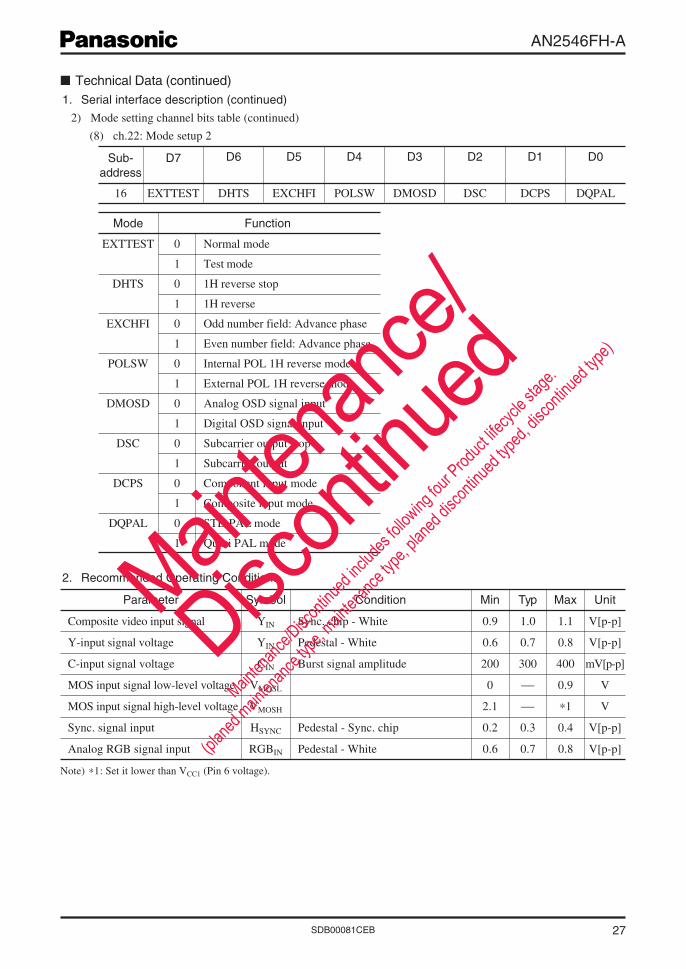
(8) ch.22: Mode setup 2
2. Recommended Operating Conditions
Sub- D7 D6 D5 D4 D3 D2 D1 D0address
16 EXTTEST DHTS EXCHFI POLSW DMOSD DSC DCPS DQPAL
Mode Function
EXTTEST 0 Normal mode
1 Test mode
DHTS 0 1H reverse stop
1 1H reverse
EXCHFI 0 Odd number field: Advance phase
1 Even number field: Advance phase
POLSW 0 Internal POL 1H reverse mode
1 External POL 1H reverse mode
DMOSD 0 Analog OSD signal input
1 Digital OSD signal input
DSC 0 Subcarrier output stop
1 Subcarrier output
DCPS 0 Component input mode
1 Composite input mode
DQPAL 0 STD PAL mode
1 Quasi PAL mode
Parameter Symbol Condition Min Typ Max Unit
Composite video input signal YIN Sync. chip - White 0.9 1.0 1.1 V[p-p]
Y-input signal voltage YIN Pedestal - White 0.6 0.7 0.8 V[p-p]
C-input signal voltage CIN Burst signal amplitude 200 300 400 mV[p-p]
MOS input signal low-level voltage VMOSL 0 0.9 V
MOS input signal high-level voltage VMOSH 2.1 *1 V
Sync. signal input HSYNC Pedestal - Sync. chip 0.2 0.3 0.4 V[p-p]
Analog RGB signal input RGBIN Pedestal - White 0.6 0.7 0.8 V[p-p]
Note) *1: Set it lower than VCC1 (Pin 6 voltage).
Mainten
ance/
Discon
tinued
Mainten
ance/D
iscont
inued
includ
es foll
owing
four P
roduct
lifecyc
le stag
e.
(planed
mainten
ance ty
pe, main
tenanc
e type,
planed
discon
tinued
typed,
discon
tinued
type)

AN2546FH-A
SDB00081CEB28
1.6001.576
1.400
1.200
1.000
0.8000.814
0.600
0.400
0.200
0 25 150
Ambient temperature Ta (°C)
Pow
er d
issi
patio
n P
D (
W)
50 75 100 1250.000
Mounted on standard board(glass epoxy: 75 × 75 × t0.8 mm3)Rth(j-a) = 79.3°C/W
Independent ICwithout a heat sinkRth(j-a) = 153.5°C/W
Technical Data (continued)3. Power dissipation of package QFP064-P-1010A
PD Ta
Mainten
ance/
Discon
tinued
Mainten
ance/D
iscont
inued
includ
es foll
owing
four P
roduct
lifecyc
le stag
e.
(planed
mainten
ance ty
pe, main
tenanc
e type,
planed
discon
tinued
typed,
discon
tinued
type)

Request for your special attention and precautions in using the technical information andsemiconductors described in this book
(1)If any of the products or technical information described in this book is to be exported or provided to non-residents, the laws and regulations of the exporting country, especially, those with regard to security export control, must be observed.
(2)The technical information described in this book is intended only to show the main characteristics and application circuit examples of the products, and no license is granted under any intellectual property right or other right owned by our company or any other company. Therefore, no responsibility is assumed by our company as to the infringement upon any such right owned by any other company which may arise as a result of the use of technical information described in this book.
(3)The products described in this book are intended to be used for standard applications or general electronic equipment (such as office equipment, communications equipment, measuring instruments and household appliances). Consult our sales staff in advance for information on the following applications: Special applications (such as for airplanes, aerospace, automobiles, traffic control equipment, combustion equipment, life support
systems and safety devices) in which exceptional quality and reliability are required, or if the failure or malfunction of the prod-ucts may directly jeopardize life or harm the human body. Any applications other than the standard applications intended.
(4)The products and product specifications described in this book are subject to change without notice for modification and/or im-provement. At the final stage of your design, purchasing, or use of the products, therefore, ask for the most up-to-date Product Standards in advance to make sure that the latest specifications satisfy your requirements.
(5)When designing your equipment, comply with the range of absolute maximum rating and the guaranteed operating conditions (operating power supply voltage and operating environment etc.). Especially, please be careful not to exceed the range of absolute maximum rating on the transient state, such as power-on, power-off and mode-switching. Otherwise, we will not be liable for any defect which may arise later in your equipment.
Even when the products are used within the guaranteed values, take into the consideration of incidence of break down and failure mode, possible to occur to semiconductor products. Measures on the systems such as redundant design, arresting the spread of fire or preventing glitch are recommended in order to prevent physical injury, fire, social damages, for example, by using the products.
(6)Comply with the instructions for use in order to prevent breakdown and characteristics change due to external factors (ESD, EOS, thermal stress and mechanical stress) at the time of handling, mounting or at customer's process. When using products for which damp-proof packing is required, satisfy the conditions, such as shelf life and the elapsed time since first opening the packages.
(7)This book may be not reprinted or reproduced whether wholly or partially, without the prior written permission of Matsushita Electric Industrial Co., Ltd.
Mainten
ance/
Discon
tinued
Mainten
ance/D
iscont
inued
includ
es foll
owing
four P
roduct
lifecyc
le stag
e.
(planed
mainten
ance ty
pe, main
tenanc
e type,
planed
discon
tinued
typed,
discon
tinued
type)