automated measurement setup
TRANSCRIPT

AUTOMATED MEASUREMENT SETUP
CU08813 S2-2013/2014
Engineering DESIGN & INNOVATION
MECHATRONIC
Author: Yongmin Qiu
Student number: 66759
Study: Mechatronics
Company: NXP Semiconductors Netherlands B.V
In-company mentor: Lude Bakema
School: HZ University of Applied Sciences
Supervisor teacher: Ad van Rijswijk

Automated measurement setup
The title of the project:
Automated measurement setup testing dimmer compatibility LED drivers
Author: Yongmin Qiu
Date: May 26, 2014
School: HZ University of Applied Sciences
Program: Mechatronics
Supervisor teacher: Ad van Rijswijk
Company: NXP Semiconductors Netherlands B.V
In-company mentor: Lude Bakema

SUMMARY
Within NXP Semiconductors the Business Line Power and Lighting Solutions (BL PLS) is
active in the area of mains AC/DC converters for power supplies (e.g. GreenChip
adapter family) and Lighting applications (e.g. drivers for Compact Fluorescent Lamps
and Solid State Lighting)
The measurement setup designed in this report can help the engineer to test the
parameter of dimmer compatibility convenient. The measurement setup includes
hardware part and software part. Through the hardware setup, the dimmer can be
controlled by software and the parameter can be measured and the result of the
measurement can be exported automatically.
The results of this research project is divided into four parts according to the Delft
Design Method. In analyze phase, the focus is on the relevant research fields. After this
phase, the dimming principle and the requirements for the setup is clear.
In concept phase, the focus is on the function tree of the setup and select ion the
concept for every function. And combine the concept for every function together.
In materialization phase, the schematic circuit of the best concept is clear. The
prototype for both hardware part and software part were made.
In the detailing phase, the test of the prototype was done and the circuit board was
installed into box. Also the user manual is written.
At the end of this project, the development of the automated test setup was not
finished completely. The test result need to be handled with software, it is not
accurate. Also the detect point is not isolated, which may cause the equipment damage.
The hardware needs to be improved to make the setup more accurate and more safety.
More details will be discussed in the main part of the report.
FOREWORD
In the last 3 months, I had an internship in NXP Semiconductors with a project to create an automated measurement setup to test the dimmer compatibility of LED driver. During this period, I have learnt a lot especially on the knowledge of electric circuit and measuring technology. This internship not only improves my professional knowledge but also makes me proud of myself and be confident for future challenge.
The structure of the report will help you find the way to better use this report:
Chapter 1: Introduction In this chapter, there are three parts involved in to describe company background, what the project is and the reason why it is carried out. Chapter 2: Theoretical framework In this chapter, the literature, theory and certain researches are written in order to show the framework of this project and the explanation of each part is prepared for being better understood. Chapter 3: Method In this chapter, the reason why the methodology is chosen and the introduction of the design methodology will be clarified. You can also find what activity is taken in the certain phase. Chapter 4: Results In this chapter, the results of each phase in the process of the project will be carried out to answer the secondary questions and show how the final prototype is designed step by step according to the chosen design methodology. Chapter 5: Discussion In this chapter, whether the solution or design meets the requirement in engineering design specification is shown. Chapter 6: Conclusion & Recommendations In this chapter, the conclusion about this project is clarified briefly for answering the main question and the recommendations is prepared for future innovation on this kind of prototype. References & Appendix The reference source from books, lectures and internet are listed and Appendixes referred in the repot are also prepared for the readers to find some more detailed information about certain part.
Finally, I would like to express my thanks to my in-company mentor, supervisory teacher and colleagues in the company. They helped me with my documentations, decisions and also gave good suggestions. It’s my honor to have the graduation internship in such a good company. I enjoyed my time working together with all nice colleagues. Thank for this internship to let me feel and learn the Netherlands’ culture and custom.
Yongmin Qiu
23th May, 2014

ABBREVIATIONS
AWG - Arbitrary Waveform Generator
DDM – Delft Design Method
DUT – Device under test
GPIB - General Purpose Interface Bus
IC - Integrated circuit
OLED - Organic light-emitting diodes
LEDs - light-emitting diodes
LDR – Light-dependent resistor
NEMA – National Electrical Manufacturers Association
PF – Power factor
PLED - light-emitting diodes
RMS - root mean square
SSL - Solid-state lighting

LIST OF CONTENTS
1. Introduction ....................................................................................................................... 1
1.1. Company background ................................................................................................ 1
1.2. Project background ................................................................................................... 1
1.3. Project introduction .................................................................................................. 2
1.4. Main question & sub question .................................................................................. 3
2. Theoretical framework ...................................................................................................... 4
3. Method .............................................................................................................................. 6
3.1. Introduction of DDM ................................................................................................. 6
3.2. Justification ................................................................................................................ 6
4. Result ................................................................................................................................. 7
4.1. Analyze Phase ............................................................................................................ 7
4.1.1. Leading edge phase cutting dimmer ................................................................. 7
4.1.2. Trailing edge phase cutting dimmer .................................................................. 9
4.1.3. Difference between leading edge dimmer and trailing edge dimmer ............ 10
4.1.4. Engineering design specification ..................................................................... 11
4.2. Concept Phase ......................................................................................................... 12
4.2.1. Function Tree ................................................................................................... 12
4.2.2. Concepts of control the dimmer by function generator ................................. 13
4.2.3. Concepts of measure conduction phase angle ............................................... 15
4.2.4. Choice of measuring equipment ..................................................................... 17
4.2.5. Final Concept & Morphological chart .............................................................. 18
4.3. Materialization Phase .............................................................................................. 18
4.3.1. Introduction of the hardware prototype ......................................................... 18
4.3.2. LDR – dimmer control ...................................................................................... 19
4.3.3. Comparator - conduction phase angle measure ............................................. 19
4.3.4. Hardware measuring circuit ............................................................................ 20
4.3.5. Connection with hardware and equipment .................................................... 21
4.3.6. Components list & Equipment list ................................................................... 21
4.4. Detailing Phase ........................................................................................................ 22
4.4.1. Software LabVIEW Programming .................................................................... 22
4.4.2. Prototype test .................................................................................................. 25
4.4.1. Hardware optimization .................................................................................... 26
4.4.2. User manual .................................................................................................... 27
5. Discussion ........................................................................................................................ 28
6. Conclusion & Recommendation ...................................................................................... 29

6.1.1. Conclusion ....................................................................................................... 29
6.1.2. Recommendation ............................................................................................ 29
References ............................................................................................................................... 30
List of Figure
Figure 1 NXP semiconductors .................................................................................................... 1 Figure 2 overview of manually testing setup ............................................................................ 2 Figure 3 block diagram of manually testing method ................................................................. 2 Figure 4 Voltage output waveform of dimmer with half cycle off time .................................... 4 Figure 5 Microcosmic circuit of dimmer .................................................................................... 4 Figure 6 Schematic of knob ....................................................................................................... 4 Figure 7 the waveform on the led bulb when flicker happen ................................................... 5 Figure 8 Inside of led bulb ......................................................................................................... 5 Figure 9 phase described in delft design method ..................................................................... 6 Figure 10 example of TRIAC....................................................................................................... 7 Figure 11 symbol of TRIAC ......................................................................................................... 7 Figure 12 example of DIAC ........................................................................................................ 7 Figure 13 symbol of DIAC type.DB3 ........................................................................................... 7 Figure 14 schematic circuit of TRIAC dimmer ........................................................................... 8 Figure 15 voltage waveform of TRIAC Z00607 (terminal2 - terminal 1) ................................... 8 Figure 16 voltage waveform of DB3 .......................................................................................... 8 Figure 17 waveform of leading edge dimming .......................................................................... 8 Figure 18 voltage waveform when ideal maximum output ...................................................... 9 Figure 19 waveform of trailing edge dimmer ............................................................................ 9 Figure 20 simulation circuit of the trailing edge dimmer .......................................................... 9 Figure 21 voltage waveform on leading edge dimmer with pure resistor load and capacitive load .......................................................................................................................................... 10 Figure 22 voltage waveform on trailing edge dimmer with pure resistor load and capacitive load .......................................................................................................................................... 10 Figure 23 function tree ............................................................................................................ 12 Figure 24 usage of LDR ............................................................................................................ 13 Figure 25 schematic circuit of LDR .......................................................................................... 13 Figure 26 schematic circuit of ideal pulse control phase cutting dimmer .............................. 13 Figure 27 schematic circuit of pulse control resistor circuit ................................................... 14 Figure 28 usage of pulse control resistor circuit ..................................................................... 14 Figure 29 overview of mechanical device ............................................................................... 14 Figure 30 waveform of opto-coupler ...................................................................................... 15 Figure 31 circuit of opto-coupler ............................................................................................. 15 Figure 32 waveform of comparator ........................................................................................ 16 Figure 33 circuit of comparator ............................................................................................... 16 Figure 34 Manually setup ........................................................................................................ 16 Figure 35 Optocoupler setup ................................................................................................... 16 Figure 36 comparator setup .................................................................................................... 16 Figure 37 Graph of conduction PF - power ............................................................................. 17 Figure 38 Graph of conduction PF – current ........................................................................... 17 Figure 39 final concept in morphological chart ....................................................................... 18 Figure 40 schematic of TRIAC dimmer .................................................................................... 18

Figure 41 outside and inside view of VTL5C6 .......................................................................... 19 Figure 42 LDR performance measuring setup ......................................................................... 19 Figure 43 result of LDR performance test ............................................................................... 19 Figure 44 schematic circuit of conduction phase angle measuring ........................................ 19 Figure 45 waveform of phase angle measured ....................................................................... 20 Figure 46 rectified waveform of voltage on DUT .................................................................... 20 Figure 47 SCHEMATIC CIRCUIT OF PROTOTYPE ...................................................................... 20 Figure 48 Diagram of hardware connection ............................................................................ 21 Figure 49 front panel of LabVIEW program ............................................................................. 22 Figure 50 block diagram of LabVIEW ....................................................................................... 23 Figure 51 Test result ................................................................................................................ 25 Figure 52 Test result processed ............................................................................................... 26 Figure 53 prototype box with circuit board inside .................................................................. 26
List of Table
Table 1 table of requirements and wishes .............................................................................. 11 Table 2 Components list & Equipment list .............................................................................. 21
List of Appendix
1. Test example ..................................................................................................................... 1
2. Measuring parameters ...................................................................................................... 1
3. LabVIEW ............................................................................................................................ 3
4. LTspice IV ........................................................................................................................... 3
5. MOSFET (Metel-oxide-semiconductor FET) ...................................................................... 3
6. Phase angle measuring circuit test result .......................................................................... 4
7. LDR performance test result ............................................................................................. 5
8. Test result .......................................................................................................................... 6
9. User Manual ...................................................................................................................... 8

1
1. INTRODUCTION
1.1. Company background
Company information
Company Name: NXP Semiconductors
NXP Semiconductors N.V. (NASDAQ: NXPI) creates solutions that enable secure connections for a smarter world. Building on its expertise in High Performance Mixed Signal electronics, NXP is driving innovation in the automotive, identification and mobile industries, and in application areas including wireless infrastructure, lighting, healthcare, industrial, consumer tech and computing. NXP has operations in more than 25 countries. [1]
Within NXP Semiconductors the Business Line Power and Lighting Solutions (BL PLS) is active in
the area of mains AC/DC converters for power supplies (e.g. GreenChip adapter family) and
Lighting applications (e.g. drivers for Compact Fluorescent Lamps and Sol id State Lighting)
1.2. Project background
NXP Semiconductors the Business Line Power and Lighting Solutions department designs the dimmable LED Driver IC for the solid state lighting solution.
Solid-state lighting (SSL) refers to a type of lighting that uses semiconductor light-emitting diodes (LEDs), organic light-emitting diodes (OLED), or polymer as sources of illumination rather than electrical filaments, plasma (used in arc lamps such as fluorescent lamps), or gas. [2]
The dimmable LED Driver IC will be used with dimmer. There are many different dimmer types from different dimmer manufacturers in the market. In this case, dimmer compatibility is a very important performance design target for new IC designs.
Dimmer compatibility means: (1) The reliability of the dimmer and the LED Driver IC are not affected by combining them. (2)Dimming behavior meets or exceeds the behavior specified in SSL7A Phase Cut Dimming for Solid State Lighting: Basic Compatibility section 3 and 4. This standard provides compatibility requirements for phase cut dimming for LED light engines and is suitable for global use. [3]
By these parameters the effect of LED Driver IC and dimmer combination are influenced:
The dimming method (forward phase cut for SSL 7A compliance)
Inrush current (to both dimmer and LED Driver)
Repetitive peak current (to both dimmer and LED Driver)
Rated Power (to both dimmer and LED Driver)
Repetitive peak ring-up voltage (at both dimmer and LED Driver)
Minimum light output (LED Driver)
Figure 1 NXP semiconductors

2
Maximum RMS current
Minimum conduction angle (dimmer)
Maximum light output (LED Driver)
Maximum conduction angle (dimmer)
Off-state dimmer supply current
On-state dimmer supply current
LED Driver IC impedance in various operating modes
Ability of the dimmer to synchronize by detecting mains zero crossing through the LED Driver IC
1.3. Project introduction
In this graduation project, I will be focus on measuring the following parameters of the LED driver with the Phase Cutting dimmer
Conduction phase angle
RMS current input
RMS voltage input
Real power input
Real power output
Apparent power output
Power factor of output power
Power loss
Power efficiency
Manual testing these items with dimmer is a time consuming task. According to Figuire2, the test engineer in the NXP needs to control the knob on the dimmer by their hand, read the measurement value on the meter and read the phase angle value on the scoop and write and the results.
Appendix 1 is the example showing how the engineers in NXP record the test results.
In this project, the aim is to design an automated measurement setup to control the dimmer, measure these seven parameters and record the results into the excel file. The user can use this setup to test these parameters automatically. The software used will be LabVIEW.
Figure 3 block diagram of manually testing method Figure 2 overview of manually testing setup

3
1.4. Main question & sub question
The main question is extracted from the assignment introduction.
Main question:
How to create a fully automated test setup that can control the dimmer, test the performance of the LED driver and export the test result?
Sub – question:
Analysis Phase
- What is dimmer?
- How does dimmer work?
- What is the difference between different type’s dimmers?
Concept Phase
- How can I control the dimmer without control the Knob?
- How can I measure the conduction phase angle?
Materialization Phase
- How to measure the performance (current, voltage, power and phase angle) of the LED driver?
- How to use LabVIEW to collect the data from the measuring equipment?
- How to export the test result?
Testing Phase
- Is there any environment requirement?
- How much type’s dimmer can this setup be used for?
4
2. THEORETICAL FRAMEWORK
Hardware
- Phase control dimming knowledge - LED bulb technology - LED driver parameter [Appendix 2] - Principle of electric circuit [4] - Electronic Device and circuit theory [5] - Measurement technology [6] - Understanding power-supply equipment - Understanding Measurement equipment - Understanding use of GPIB [7]
Software
- Software development environment Labview [Appendix 3]
- Software simulation environment LTspice IV [Appendix 4]
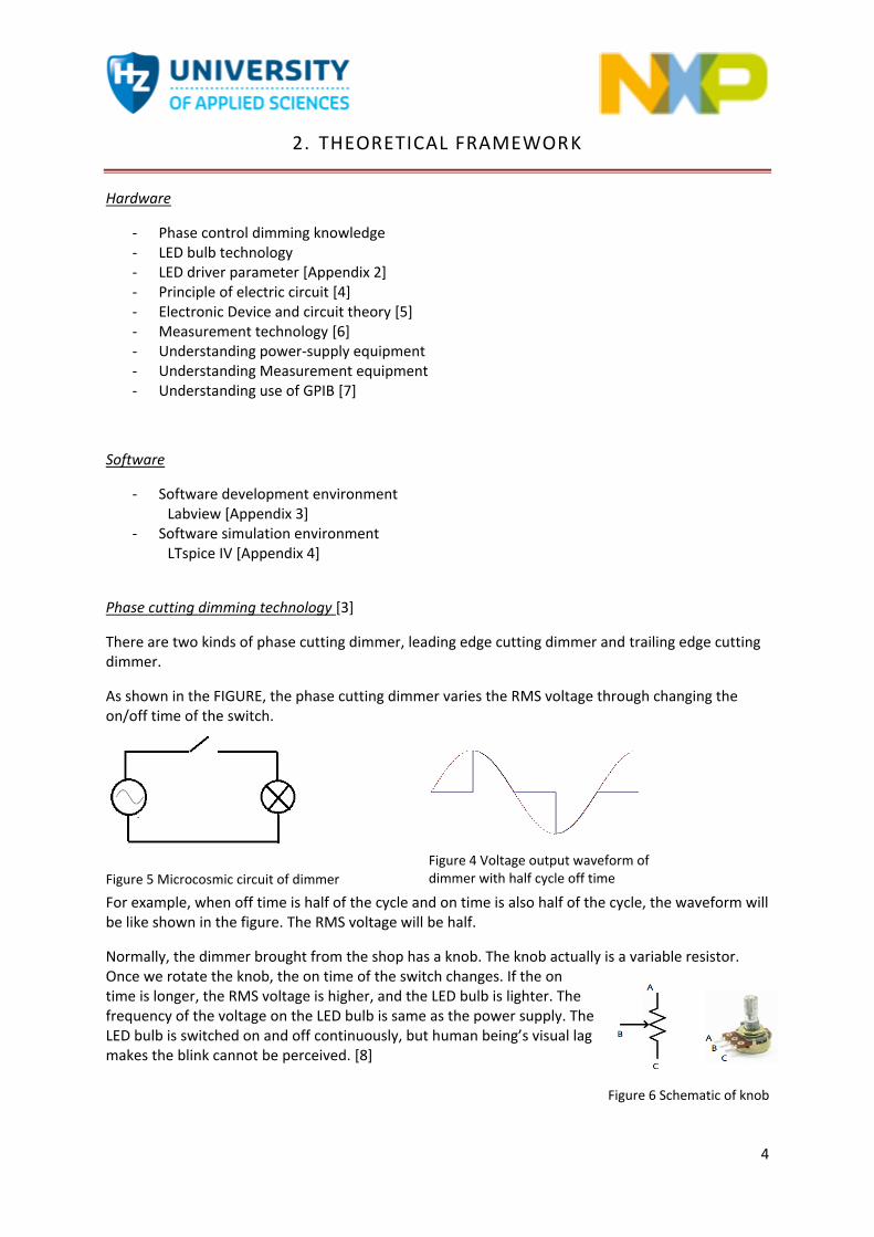
Phase cutting dimming technology [3]
There are two kinds of phase cutting dimmer, leading edge cutting dimmer and trailing edge cutting dimmer.
As shown in the FIGURE, the phase cutting dimmer varies the RMS voltage through changing the on/off time of the switch.
For example, when off time is half of the cycle and on time is also half of the cycle, the waveform will be like shown in the figure. The RMS voltage will be half.
Normally, the dimmer brought from the shop has a knob. The knob actually is a variable resistor. Once we rotate the knob, the on time of the switch changes. If the on time is longer, the RMS voltage is higher, and the LED bulb is lighter. The frequency of the voltage on the LED bulb is same as the power supply. The LED bulb is switched on and off continuously, but human being’s visual lag makes the blink cannot be perceived. [8]
Figure 5 Microcosmic circuit of dimmer
Figure 4 Voltage output waveform of dimmer with half cycle off time
Figure 6 Schematic of knob

5
LED bulb
LED bulb is a combination of one LED Driver and one or more LED string. The LED Driver IC and the LED string will be integrated into a single unit.
Now the biggest issue of the TRIAC dimmable LED is dimmer compatibility. For most families, conventional TRAIC dimmer is commonly used, which is produced for conventional high power incandescent bulb. A LED bulb is low energy power (less than 20W) consumption bulb, while it has to interact with those dimmers composed for the higher powers of conventional bulb. When a LED bulb is used under leading edge dimmer, the current is so low because of the low load that it is easy to be lower than the holding current of the TRIAC, in that case visible flicker is foreseen.
Needed knowledge for understanding, designing and engineering electric circuits: [9] [10] The electric circuit knowledge above will be used though this whole project.
Ohms laws and simple resistive circuits, Kirchoff laws circuit elements, voltage and current sources Sign conventions, Loop and Nodal analysis, Thevenins & Norton Theorems Properties of inductors and capacitors AC circuit analysis, impedance and admittance calculations Power calculations real, reactive and complex, three phase circuits
Electronic Device and circuit theory [4]
The knowledge of the electronic components like diodes, transistor, thyristor, resistor, capacitor, inductive devices, optoelectronic devices and etc. will be used in this project.
Measurement technology [6]
In this project, some measurement devices such as multimeter, power meter and scoop will be used, which are all part of the Measurement technology.
Power-Supply Equipment
- Function generator [11] - AC/DC power supply
LabVIEW [12]
The software for the control of the several equipment will be programmed in the software development environment of Labview(Described in Appendix 3).
Figure 8 Inside of led bulb Figure 7 the waveform on the led bulb when flicker happen

6
3. METHOD
3.1. Introduction of DDM
Delft Design Methodology will be applied through this whole project. Phases of Delft Design Methodology have a good fit for the process of this project. With this methodology, sub questions will be solved one by one until the main question is accomplished. [13]
The Delft Design Method (DDM) is the method that provides a systematic and goal-oriented structure for designing also for managing the workflow for the project.
Figure 9 phase described in delft design method
As shown in Figure 9, we can see the whole version of the Delft Design Method. In the phase of project planning, research on background should be done. Concepts are generated from the deeper research on topics and requirements from costumer in the phase of analyzing, also from idea brainstorm in the concept phase. Through concepts evaluation, the best concept can be chosen. In materialization phase, practical problems are solved and provide reliable fundament for product optimization in the detailing phase.
3.2. Justification
This part is focusing on explanation on the reason why Delft Design Method is chosen for applying in the project.
DDM, one of the main courses for the major of Mechatronics, have been applied in previous project before, which leads to skilled application.
Relating to the project, as shown in the Introduction, the main task for the project is a combination of hardware and software but more weighted on the hardware part. So the method I choose should be involved with at least one phase for practical product development. From the figure 9, we can see that both materialization and detailing phase of DDM are for product development.

7
4. RESULT
4.1. Analyze Phase
In this phase, the research on the project is done and the Engineering Design Specification is made.
4.1.1. Leading edge phase cutting dimmer
Leading edge phase cutting dimmer is also called forward phase control/cutting dimmer. Thyristors are the main electronic switches used on it, and TRIAC is the most representative one.
TRIAC (Triode for Alternating Current)
The TRIAC is an electronic component that can conduct current in either direction when it is triggered (turned on). [14]
When there is a “turn on” current go through the G terminal, the TRIAC is switched on at both forward and reverse biased. Then, there is current through A2 and A1 terminals. The minimum turn on current is called gate threshold current and is indicated by IGT.
However, the TRIAC cannot be switched off by current through the G terminal. Only the current go through the A2 and A1 terminal is lower than a certain current, it turns off. That current is called holding current and is indicated by IH. [15] [16]
DIAC (Diode for Alternating Current)
DIAC is commonly used to control the current go through the G terminal on the TRIAC in the leading edge phase cutting dimmer.
Figure 11 symbol of TRIAC
Figure 13 symbol of DIAC type.DB3
Figure 10 example of TRIAC
Figure 12 example of DIAC

8
The DIAC is a diode that conducts current only when the voltage across the DIAC is higher than its breakover voltage, VBO. The DIAC with type nr DB3 is commonly used by manufacturers for dimmers. The breakover voltage of the DB3 from STMicroelectronics is 32V.
The red square in figure 14 shows the schematic circuit of an actual TRIAC dimmer. The conduction phase angle is controlled by the TRIAC, so as to vary the RMS voltage and the RMS current passing the LED bulb. Then the brightness change is realized.
As shown in figure 15,16 and 17,When the voltage on the DIAC (equals to the voltage on C1) get the breakover voltage of it, the current can pass the DIAC into the G-terminal of the TRIAC. The TRIAC (terminal 2 – terminal 1) can be conducted. After that, the capacitor C1 will discharge, the voltage on the DIAC will be reduced. But the TRIAC will keep conduct until the current pass (terminal 2 – terminal 1) lower than holding current.
Figure 17 waveform of leading edge dimming
Figure 14 schematic circuit of TRIAC dimmer
Figure 16 voltage waveform of DB3 Figure 15 voltage waveform of TRIAC Z00607 (terminal2 - terminal 1)

9
Through the variable resistor, the time of the voltage on the DIAC getting breakover voltage can be changed so that the time of the TRIAC switching on can be controlled. When the variable resistor becomes bigger, the conduction phase angle becomes smaller, the RMS voltage pass the LED bulb will be smaller. The maximum value of the variable resistor determines the minimum output rms voltage value of the dimmer. The R_protect resistor determines the maximum output rms voltage value of the dimmer. When R_protect and variable resistor both set to 0Ω, the TRIAC output waveform will still not be full sine wave. Because the DIAC needs breakover voltage to give the control signal to the TRIAC. When DB3 is used, the ideal maximum conduction phase angle will be about 354.8⁰.
𝐼𝑑𝑒𝑎𝑙 𝑚𝑎𝑥 𝑝ℎ𝑎𝑠𝑒 𝑎𝑛𝑔𝑙𝑒
= 3600 − 𝑎𝑟𝑐𝑠𝑖𝑛 (32
230 × √2)
4.1.2. Trailing edge phase cutting dimmer
Trailing edge phase cutting dimmer is also called the reverse phase control dimmer or transistor dimmer. It is less common however than leading edge phase cutting dimmer. This is because it is more expensive to make and need to incorporate a pair of MOSFET’s [Appendix 5]or IGBTs whereas a leading edge phase cutting dimmer is based around a single TRIAC. The dimming principle is similar to thyristor dimming, but the turn-on switch is transistor. As shown in the figure 20, the switch of MOSFET turn on when the pulse is on, and it turns off when the pulse is off. So the signal
output is fully controlled by the control pulse.
Figure 18 voltage waveform when ideal maximum output
Figure 19 waveform of trailing edge dimmer Figure 20 simulation circuit of the trailing edge dimmer

10
4.1.3. Difference between leading edge dimmer and trailing edge dimmer
Leading edge dimmer
The electrical current (sinusoidal signal) is turned off at the front of the AC input waveform immediately after the zero crossing
Traditionally used for incandescent lamps or magnetic low voltage transformers
Produces a quick inrush of voltage into the load every half cycle which leads to a high inrush current into the electronic components of the LED lamp
Causes buzzing sound when dimmed
The performance of the trailing edge dimmer under capacitive loads condition will be same with it under resistive load condition. [8] [17] [18]
As shown in figure 21, the blue curve is the voltage on a resistive load and the red curve is the voltage on a capacitive load has a resistive as well as a capacitive load component. These two curves are the same.
Because of the voltage on the capacitive components in load rise too fast when the TRIAC is switched on, the buzzing sound will be caused by the capacitor in the load.
Trailing edge dimmer
The electrical current (sinusoidal signal) is turned off at the end of the AC input waveform immediately before the zero crossing
Traditionally used for electronic drivers or low voltage transformers (capacitive loads)
Is not subject to a high inrush of voltage that leads to a high inrush of current
Does not cause buzzing sound when dimmed
The performance of the trailing edge dimmer under capacitive loads condition will be different from it under resistive load condition.
As shown in figure 22, the blue curve is the voltage on a resistive load and the red curve is the voltage on a load has a resistive as well as a capacitive load component.
Because the capacitive components discharge during the phase cutting time in the load, the voltage will drop down smooth. That’s why there will be no buzzing sound when dimmed under a trailing edge phase cutting dimmer.
Figure 21 voltage waveform on leading edge dimmer with pure resistor load and capacitive load
Figure 22 voltage waveform on trailing edge dimmer with pure resistor load and capacitive load

11
4.1.4. Engineering design specification
In this part is described on which requirements the setup should meet. By contacting with the In-company mentor Lude Bakema, I divide all the requirements and wishes into 6 sessions. All of those requirements and wishes are the key things I have to follow throughout the whole designing phases, which makes sure I will do the right thing.
Table 1 table of requirements and wishes
Requirements Explanation
Safety
It is safe to user. The measurement setup should be safe to the user and it should not damage the equipment during the test.
It is safe to equipment.
Installation
It should be installed in 5 minutes. The measurement setup should be easy to install and connected with the equipment. During the installation, the setup should not damage the dimmer and the LED bulb.
It should be installed by any staff in the company.
The dimmer or the LED bulb should not be damaged during the installation.
Environment
It should be used in the normal environment
(temperature with 10 – 40) The setup will be used by engineer in the Lab.
It should be used in the Lab
Equipment The equipment will be easy to get.
All the equipment can be found in the Lab
Control The test will be processed by the program automatically. The dimmer can be controlled by computer.
Measure
The error of measuring result of conduction phase angle can be lower than 0.1ms.
The error of the measurement must be lower than 1%. (requirements from in-company mentor) The calculation formula of the power loss and power efficiency must be correct.
The error of measuring result of RMS current input can be lower than 0.5mA.
The error of measuring result of RMS voltage input can be lower than 0.3V.
The error of measuring result of power can be lower than 0.05w.
The error of measuring result of power factor can be lower than 0.1
The calculated result of power loss should be correct.
The calculated result of power efficiency should be correct.
The LabVIEW program can read the measuring result from the equipment.
The measuring results can be saved into excel file.
12
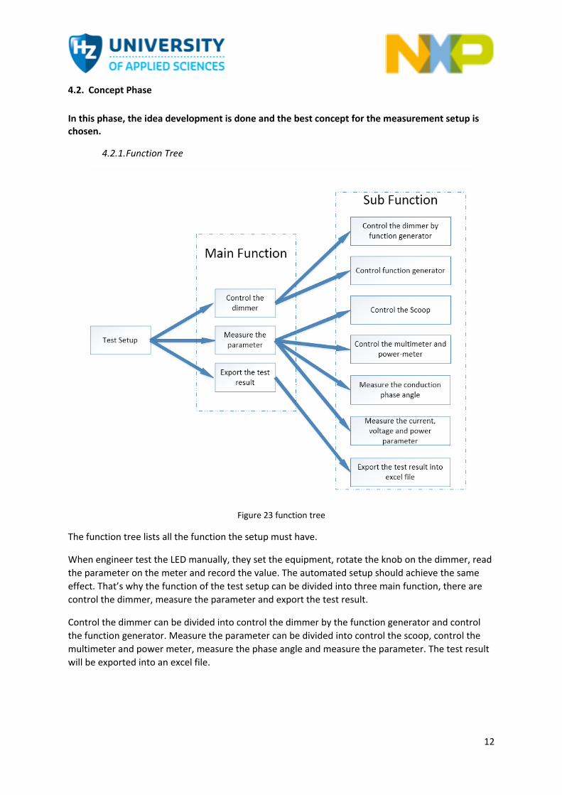
4.2. Concept Phase
In this phase, the idea development is done and the best concept for the measurement setup is chosen.
4.2.1. Function Tree
Figure 23 function tree
The function tree lists all the function the setup must have.
When engineer test the LED manually, they set the equipment, rotate the knob on the dimmer, read
the parameter on the meter and record the value. The automated setup should achieve the same
effect. That’s why the function of the test setup can be divided into three main function, there are
control the dimmer, measure the parameter and export the test result.
Control the dimmer can be divided into control the dimmer by the function generator and control
the function generator. Measure the parameter can be divided into control the scoop, control the
multimeter and power meter, measure the phase angle and measure the parameter. The test result
will be exported into an excel file.
13
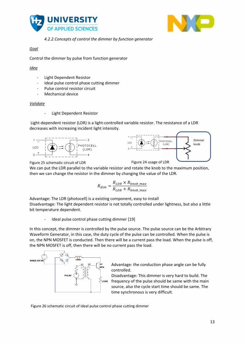
4.2.2. Concepts of control the dimmer by function generator
Goal
Control the dimmer by pulse from function generator
Idea
- Light Dependent Resistor - Ideal pulse control phase cutting dimmer - Pulse control resistor circuit - Mechanical device
Validate
- Light Dependent Resistor
Light-dependent resistor (LDR) is a light-controlled variable resistor. The resistance of a LDR decreases with increasing incident light intensity.
We can put the LDR parallel to the variable resistor and rotate the knob to the maximum position, then we can change the resistor in the dimmer by changing the value of the LDR.
𝑅𝑑𝑖𝑚 =𝑅𝐿𝐷𝑅 × 𝑅𝑘𝑛𝑜𝑏_𝑚𝑎𝑥
𝑅𝐿𝐷𝑅 + 𝑅𝑘𝑛𝑜𝑏_𝑚𝑎𝑥
Advantage: The LDR (photocell) is a existing component, easy to install Disadvantage: The light dependent resistor is not totally controlled under lightness, but also a little bit temperature dependent.
- Ideal pulse control phase cutting dimmer [19]
In this concept, the dimmer is controlled by the pulse source. The pulse source can be the Arbitrary Waveform Generator, in this case, the duty cycle of the pulse can be controlled. When the pulse is on, the NPN MOSFET is conducted. Then there will be a current pass the load. When the pulse is off, the NPN MOSFET is off, then there will be no current pass the load.
Advantage: the conduction phase angle can be fully controlled. Disadvantage: This dimmer is very hard to build. The frequency of the pulse should be same with the main source, also the cycle start time should be same. The time synchronous is very difficult.
Figure 25 schematic circuit of LDR Figure 24 usage of LDR
Figure 26 schematic circuit of ideal pulse control phase cutting dimmer
Dimmer knob

14
- Pulse control resistor circuit
Control the duty cycle of an external high frequency DC source to control the MOSFET, which can change the resistor in the circuit.
The Arbitrary Waveform Generator can be used like a pulse source, which can set the frequency to the 1k hz and control the duty cycle from 0.01% - 99.9998%.
We can see from the picture in the right. The pulse can control the mosfet directly, which can switch the small resistor on and off. When we set the frequency to 0.01%, the resistor out put will be about 470K ohm. When we set the frequency to the 99.9998% the resistor output will be about 100ohm.
That how we can control the resistor by using the pulse control resistor circuit.
The usage of this is soldering the knob off, rotating it to the maximum value and soldering it on this circuit. Put both two knob nodes to the position where the original knob pin is.
𝑅𝑑𝑖𝑚 = (1 − 𝐷𝑢𝑡𝑦 𝐶𝑦𝑐𝑙𝑒) × 𝑅𝑘𝑛𝑜𝑏_𝑚𝑎𝑥
Advantage: The resistor is stable than LDR.
Disadvantage: The knob will be soldered off. The dimmer is broken.
- Mechanical device
We can make a small mechanical device which include a motor and a belt, we can use the computer to control the motor rotating, so the belt connected with the motor will rotate the knob. So we can control the knob automatically.
Advantage: The knob on the dimmer can be controlled visibly.
Disadvantage: Build this mechanical device is difficult.
Figure 27 schematic circuit of pulse control resistor circuit
Figure 28 usage of pulse control resistor circuit
Figure 29 overview of mechanical device
Dimmer knob

15
Compare
Concept Advantage Disadvantage
Light Dependent Resistor Existing components, easy to install
The LDR has a little temperature dependent
Ideal pulse control phase cutting dimmer
Conduction phase angle is totally under controlled
Hard to build, the time synchronous is a problem
Pulse control resistor circuit
The resistor is stable than LDR
Installation is more complex than LDR, the knob should be soldered off.
Mechanical device The knob on the dimmer can be controlled visibly.
Hard to build, there is no motor in the lab.
Conclusion
The Light Dependent Resistor will be chosen to control the dimmer. Because we have this existing components in the lab. It is easy to install. Since the LDR is a little bit temperature dependent, but the relation between the duty cycle and the power is not important. We choose to use phase angle as varying input parameter. When we can measure this accurately we can compensate for (temperature) variations.
4.2.3. Concepts of measure conduction phase angle
Goal
Through electrical circuit, transfer the conduction phase angle into a pulse, because the scoop can read the pulse width. In this case, the conduction phase angle can be read by scoop.
𝑐𝑜𝑛𝑑𝑢𝑐𝑡𝑖𝑜𝑛 𝑝ℎ𝑎𝑠𝑒 𝑎𝑛𝑔𝑙𝑒 = 180° − 𝑓𝑟𝑒𝑞𝑢𝑒𝑛𝑐𝑦 × (𝑤𝑖𝑑𝑡ℎ +) × 180°
Width+ unit: s
Idea
- Opto-coupler - Comparator
Validate
- Opto-coupler
As shown in the figure 30, when the voltage input is about 0, the LED in the optocoupler is off so that the transistor in the optocoupler is off. The voltage level at point probe detecting will be 5V.
Figure 31 circuit of opto-coupler Figure 30 waveform of opto-coupler
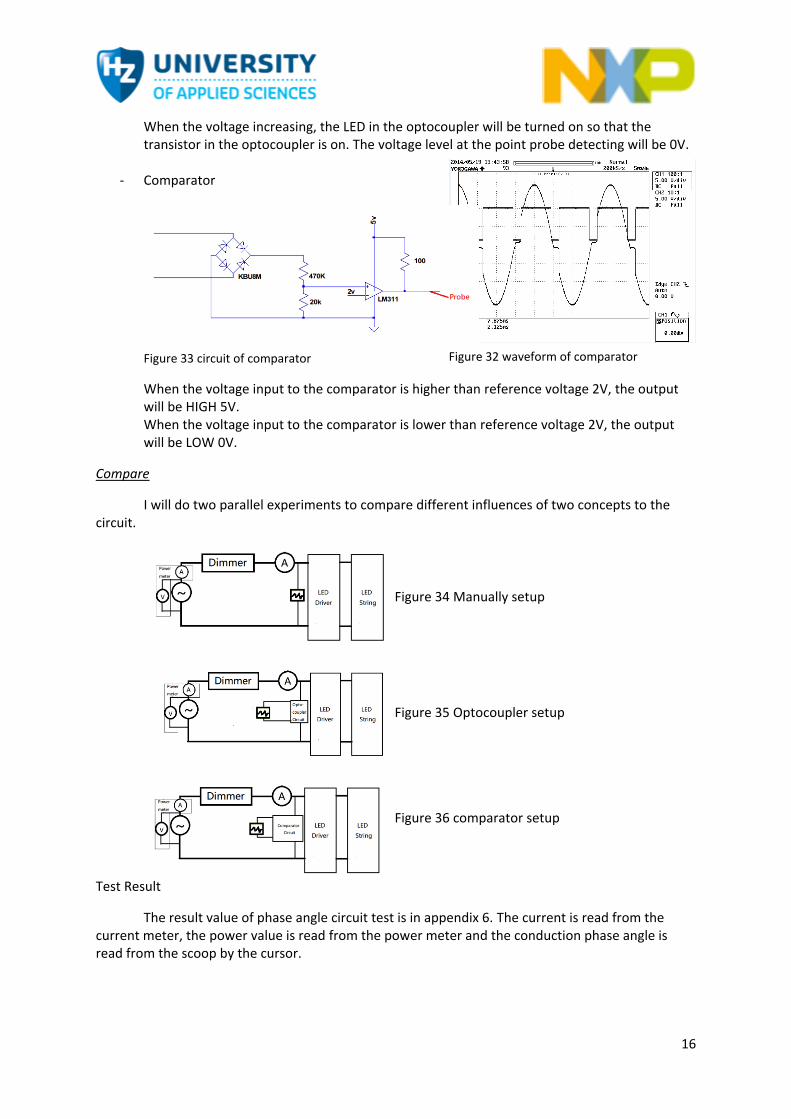
16
When the voltage increasing, the LED in the optocoupler will be turned on so that the transistor in the optocoupler is on. The voltage level at the point probe detecting will be 0V.
- Comparator
When the voltage input to the comparator is higher than reference voltage 2V, the output will be HIGH 5V. When the voltage input to the comparator is lower than reference voltage 2V, the output will be LOW 0V.
Compare
I will do two parallel experiments to compare different influences of two concepts to the circuit.
Figure 34 Manually setup
Figure 35 Optocoupler setup
Figure 36 comparator setup
Test Result
The result value of phase angle circuit test is in appendix 6. The current is read from the current meter, the power value is read from the power meter and the conduction phase angle is read from the scoop by the cursor.
Figure 33 circuit of comparator Figure 32 waveform of comparator

17
From the test result, we can see the result from the comparator circuit is more close to the manually result. Because the optocoupler non-isolated side will cost more current from the main circuit, which will influence the main circuit. In the other hand, the comparator has its own external supply which will not cost much current from the main circuit, so it will influence less to the main circuit.
Conclusion
The comparator circuit is chosen to measure the conduction phase angle, because it can convert the conduction phase angle into pulse, also it has less influence on the main circuit.
4.2.4. Choice of measuring equipment
Choice
Power supply
Agilent 6812B
Function Generator
Agilent 33220A
Multimeter
Keithley 2000
Power meter
YOKOGAWA WT210
Scoop
YOKOGAWA DL1640L
Reason
The reason why these measuring equipment chosen is because we have more stable
LabVIEW driver for them. With these LabVIEW drivers, these measuring equipment can be
controlled by LabVIEW.
Figure 38 Graph of conduction PF – current Figure 37 Graph of conduction PF - power

18
4.2.5. Final Concept & Morphological chart
Figure 39 final concept in morphological chart
The blue line in figure 39 is the final concept for every sub function, the Agilent 6812B is chosen for the power supply, the light dependent resistor and Agilent 33220A is chosen to control the dimmer. The comparator circuit and YOKOGAWA DL1640L are used to measure the conduction phase angle. The multimeter Keithley 2000 is used to measure the current and voltage. The YOKOGAWA WT210 is used for measure the power. LabVIEW will be used to control the measuring equipment and export the test result.
4.3. Materialization Phase
In this phase, the prototype of hardware is made.
4.3.1. Introduction of the hardware prototype
The hardware prototype is based on a leading edge TRIAC dimmer. The schematic circuit of this TRIAC dimmer is in FIGURE. The concept of controlling the dimmer and the concept of measuring conduction phase angle will be combined with this dimmer. So after combined, this hardware prototype can be controlled by function generator and the conduction phase angle of the output will be converted into a pulse width which can be easily measured by a scoop.
The prototype made can be used to automated control the dimmer and measure the current input to the LED driver and the real power output, appearant power output, power factor from the mains.
Figure 40 schematic of TRIAC dimmer

19
4.3.2. LDR – dimmer control
The LDR type VTL5C6 is chosen to control the dimmer. Refer to the datasheet, the range of the resistor value of it is 2kΩ to 100MΩ.
Here is the test circuit for testing the performance of the LDR. The maximum current of it in the datasheet is 40mA. So the resistor 10KΩ,10K5Ω,11KΩ and 12K were chosen to series with the LED side. The duty cycle of the pulse were set from 0-100%. The resistor value of the LDR can be measured by multimeter. The test result can be found in the Appendix 7.
From the test result, we can see the resistor value change most at duty cycle with 0% - 10%. That’s why I put the x-axis into logarithmic scale. It can be clearer to see the different performance with the different current at LED side.
4.3.3. Comparator - conduction phase angle measure
Figure 44 schematic circuit of conduction phase angle measuring
The circuit in the figure 44 is the conduction phase angle measuring circuit with comparator, the input of the comparator cannot be high voltage, so voltage divider is used to reduce the voltage making it small enough. Also there is only one DC supply, so another voltage divider is used to create
Figure 41 outside and inside view of VTL5C6
Figure 42 LDR performance measuring setup
Figure 43 result of LDR performance test

20
the reference voltage from the voltage supply. The resistor 2k2 is used for creating the current to pull-up the output voltage. This resistor cannot be small, because of the voltage divider, the ground of the output is connected with the ground of reference voltage.
Here is the voltage waveform after the bridge-rectifier, we can see the waveform has a tendency to increase during the phase cutting time. This phenomenon is caused by the capacitor in the led driver. If the load is a pure resistor load, it will not happen. But the SSL LED driver has capacitive components inside. This capacitive components will discharge during the cutting , the reference voltage must be increased to avoid this increase voltage being detected. The disadvantage is the same voltage level at the end of the cycle cannot be detected also. The conduction phase angle (pulse width) measured will be about 0.4ms lower than the actual value.
4.3.4. Hardware measuring circuit
The schematic circuit of the final circuit which combined concept together is in the following. In this circuit, the dimmer can be controlled by function generator and the conduction phase angle can be measured by the pulse width on the scoop.
Figure 47 SCHEMATIC CIRCUIT OF PROTOTYPE
Phase Angle missing
Conduction phase angle measuring
Dimmer
Light Dependent Resistor Light Dependent Resistor
Conduction phase angle measuring circuit
Dimmer
Pulse_IN -
Pulse_IN +
Probe Detect Point
Mains_N
DC_in – (GND)
DUT-
DC_in+
DUT+ Mains_ L
Figure 45 waveform of phase angle measured Figure 46 rectified waveform of voltage on DUT

21
4.3.5. Connection with hardware and equipment
Figure 48 Diagram of hardware connection
The diagram about how the hardware prototype connected with the equipment is shown in the figure.
All the equipment but the DC source are connected with the PC through GPIB, so that LabVIEW can switch and set the value of them. The DC source needs to set manually, because DELTA ELEKTRONIKA ES 030-5 don’t have the GPIB connection.
4.3.6. Components list & Equipment list
Table 2 Components list & Equipment list
Components list Equipment list
- TRIAC Z0067 - DB3 - Variable resistor 470K - Resistor 22K - Optocoupler - Light Dependent
Resistor - Bridge Rectifier - Capacitor 100n - Inductor 100m
- Power supply – Agilent 6812B - Arbitrary Waveform Generator – Agilent 33220A - Scoop – YOKOGAWA DL1640L - Multimeter - Keithley 2000 - Power meter - YOKOGAWA WT210 - DC-power source - DELTA ELEKTRONIKA power supply
ES 030-5

22
4.4. Detailing Phase
In this phase, software program, the test on the prototype and prototype development are conducted.
4.4.1. Software LabVIEW Programming
As told before, LabVIEW was used to control the dimmer and equipment for the testing. Also it can read the measuring value and export into the excel file. The LabVIEW program consists of front panel part and block diagram part. [20]
Front panel
The front panel of LabVIEW is shown in the figure 49, consists of nine parts. They are equipment address panel, power supply panel, status and progress panel, buttons, error panel, function generator panel, excel export, 2D-array and xy graph.
Figure 49 front panel of LabVIEW program
① ② ③ ④
⑤
⑥
⑦
⑧
⑨
① Equipment address panel, user need to control the GPIB address for every equipment in this panel.
② Power supply panel, user can set the amplitude and the frequency of the mains AC supply in this panel.
③ Status& progress panel, if the test is running, it will show “testing” and the duty cycle will show the progress.
④ Buttons, switch on or switch off the test.
⑤ Error panel, user can see if there is any error happened.
⑥ Function generator – duty cycle panel, set the duty cycle range and step of the test.
⑦ Excel export, user can choose the sheet path, and the save path in this panel.
⑧ Test result array, the test result can be seen in this 2D-array.
⑨ Conduction phase angle – current graph, the relation of the phase angle and current will be shown in this xy graph.

23
Block diagram
The overview of block diagram of LabVIEW is shown in the following figure.
Figure 50 block diagram of LabVIEW
① Read the GPIB address from the front panel and initialize all the equipment.
② Set the duty cycle of the output pulse from the function generator.
③ Delay till the LDR and the measuring meters stable.
④ Read the current value from current meter and transfer the unit into mA.
⑤ Read the conduction phase angle from scoop, calculate the value in unit degree.
⑥ Read the real power, apparent power and power factor from the power meter.
⑦ Store all the measuring result into array.
⑧ Show the result on the XY graph.
⑨ Close all the equipment.
⑩ Read the sheet from the sheet path, write the test result into the sheet and save the test result as an excel file at save path.
Testing status
Waiting status
①
②
③
④
⑤
⑥
⑦
⑧
⑨
⑩

24
Flowchart of block diagram
This is the flowchart of the LabVIEW program. In this chart, we can tell the test have been done forward and reverse twice, the duty cycle will be from start to final and from final to start due to the LED driver need a start current to launch. In this test method, we can easily read the start current of device under test.
Set the duty cycle range
Do the test from start- final
Do the test from final - start
Save the test result
END

25
4.4.2. Prototype test
Test condition
Temperature 25
Equipment connection diagram
All the equipment are connected by LabVIEW through GPIB.
Device under test
LED driver – NXP SSL21082
LED string – NXP BSX01211
Software configuration
Mains supply – 230V 50HZ
Test Range – duty cycle 0 - 100 Test step 0.1
Test result
The test result is shown in the appendix 8.
Figure 51 Test result

26
Figure 52 Test result processed
From the picture above we can see the automated test result is not fit with the manually test result. The reason is because what mentioned in chapter 4.3.3. There are 0.4ms phase angle missing because of the high reference voltage on the comparator. After process the test result, add that 0.4ms to the phase angle, the test is shown in the Figure 50. The parameter measured hit the requirements.
4.4.1. Hardware optimization
After test done, the test result is acceptable. A box was made for install the circuit board. With the connector on the box, this hardware prototype can be easy to connect the LED bulb and the measuring equipment for doing the test.
Figure 53 prototype box with circuit board inside
The figure below shown how the circuit board installed in the box. Also the way how the wires and probe can be connected with the box easily is shown in the figure 53.
Left view
Right view

27
4.4.2. User manual
The user manual is written to the user who will use this setup to do the test. The diagram of the
hardware connection and the usage of the software are both written in the user manual.
The user manual is in the appendix 9.
Following the user manual, the user can connect the hardware with the equipment, set the GPIB
address in a right way and launch the LabVIEW program to do the test in a safe position.

28
5. DISCUSSION
For the safety
The measurement setup is safe to the user if the user is following the user manual. But we cannot exclude the potential safety hazard to the equipment even if user follow the user manual completely, because the detect point of the scoop is not isolated with the mains.
For the installation
The prototype is easy to connect with the wires and probe of the equipment and the test LED driver.
For the environment
The measurement can be used in the lab with normal temperature (10 - 40)
For the equipment
The measuring equipment chosen can be controlled by the LabVIEW. Also these equipment are available in the lab. The equipment used are a mains power supply, a scoop, a multimeter, a power meter, a function generator and a DC power supply.
For control the dimmer
The dimmer is essentially controlled by the variable resistor. So the light dependent resistor is used to parallel to the resistor. The light dependent resistor is an existed components, which has a small led inside. In this case, as the input current increasing, the light dependent resistor value will decrease, so the total resistance will change, and the dimmer control is realized.
For measure the parameter
Till this report was written, the conduction phase angle measured by the setup is not accurate, the error was about 0.3-0.4ms. The reason was the high reference voltage to the comparator mentioned in the chapter 4.3.3. The comparator can detect the start time of on-state (LED) accurate, but it cannot detect the end time of on-state (LED), which cause the conduction phase angle is not accurate. The comparator output the LOW signal when the voltage on the LED is lower than about 50V. But if we need an accurate conduction phase angle, the signal out should be LOW when the voltage on the LED is about 0V.
The current, power parameter measured is accurate, because of the using comparator, the big resistor is serious in the circuit, so the influence of the conduction phase angle measuring circuit is small. The power cost on the conduction phase angle measuring circuit is lower than 0.5w.
For my measurement setup, only current input, mains power, mains apparent power, power factor and conduction phase angle is measured, because the equipment I have is limited. The power input, power output, voltage input can be measured with the same concept if there are more equipment.

29
6. CONCLUSION & RECOMMENDATION
6.1.1. Conclusion
In conclusion, the main question of the project is to create a fully automated test setup that can control the dimmer, test the performance of the LED driver and export the test result. The test setup can be divided into hardware part and software part.
The software works well, all the equipment used can be controlled and the value measured can be read by LabVIEW through GPIB. The test result can be exported into excel file.
Through the hardware, the dimmer can be controlled by light dependent resistor with the pulse from the function generator, also the conduction phase angle can be transferred in to pulse through comparator. Due to the equipment limitation, only the current input, the real power, apparent power and power factor of mains output can be measured.
Under the manually test, it will cost 1 minute every step. Under the automated measurement setup, it will cost only 10 seconds every step, during the test, the engineer don’t need to stay beside which is quite time-saving. If there are more multimeter and power meter, the parameter like voltage input, real power input, real power output, apparent power output, power factor of output power, power loss, and power efficiency can be measured by this measurement setup.
The problem is the conduction phase angle measured is not very accurate (about 0.3-0.4ms error), also the detect point for the scoop is connected with the mains supply, which has a safety risk.
6.1.2. Recommendation
For the safety on the equipment
Since the detect point of the scoop is connected with the mains, there will be a safety risk to the
equipment. The easy way to make the detect point safe is to isolate it with the mains supply by
optocoupler. In this way, another external DC supply is needed. The DC supply will be used on the
isolated part. Note that, the DC supply used on the optocoupler cannot be used on the comparator.
Because the comparator is connected with mains supply, if that DC supply connected with it, then
the optocoupler cannot be an electrical-isolate role, so It cannot protect the equipment.
For the conduction phase angle measuring
Now the error of conduction phase angle measuring is caused by the high reference voltage on the
comparator, so the comparator cannot detect the zero (end of cycle) accurate. But It can detect the
start time of the conduction phase angle accurate. So what we need to do it design another circuit
(for example optocoupler) to detect the zero of the end cycle. Then we use a RS flipflop, the output
of the comparator is Set, the output of the zero detection is Reset, the output of the flipflop will a
pulse, the pulse width+ will the accurate conduction phase angle.

30
REFERENCES
[1] Wikipedia, "NXP Semiconductors," [Online]. Available: en.wikipedia.org/wiki/NXP.
[2] Wikipedia, "Solid-state lighting," Wikipedia, 2014. [Online]. Available: http://en.wikipedia.org/wiki/Solid-state_lighting. [Accessed 20 2 2014].
[3] NEMA Standards Publication SSL 7A-2013, Phase Cut Dimming for Solid State Lighting: Basic Compatibility, National by National Electrical Manufacturers Association, 2013.
[4] N. L. &. M. F. Boylestad R. L., Electronic devices and circuit theory, Pearson Prentice Hall.
[5] T. L.Floyd, Digital Funamentals Tenth Edition, 2011.
[6] X. x. X. Y. Xu Shukai, "Present application situation and development tendency of synchronous phasor measurement technology based wide area measurement system," National Power Dispatch & Communication Center, Beijing, 2009.
[7] Wikipedia, "IEEE-488," [Online]. Available: https://en.wikipedia.org/wiki/GPIB.
[8] Fairchild semiconductor, "AN-9745 Design Guide for TRIAC Dimmerable LED Driver Using FL7730," 2013.
[9] J. W. Nilsson, "Electric Circuits Ninth Edition," 2012.
[10] J. W. &. R. S. A. Nilsson, "Electric circuits(Vol. 8)".Prentice Hall.
[11] Wikipedia, "Function generator," Wikipedia, 2014. [Online]. Available: http://en.wikipedia.org/wiki/Function_generator. [Accessed 14 3 2014].
[12] J. G.W., "LabVIEW graphical programming: practical applications in instrumentation and control," 1997.
[13] J. D. J. Z. R. v. d. S. Annemiek van Boeijen, "Delft Design Guide," 2013.
[14] D. L. B. Rand, "Issues, models and solutions for triac modulated phase dimming of LED lamps," 2007.
[15] Philips Semiconductors, "Thyristors and Triacs," Technical Publications, 1997.
[16] P. Semiconductors, "Power control with Thyristors and Triacs," Power Semiconductor Applications, vol. 6, 1994.
[17] P. Green, "IRPLHALO1E revB," 2005.

31
[18] G. Harper, "Trailing edge or leading edge LED dimming," 2013. [Online]. Available: http://www.leapfroglighting.com/trailing-edge-or-leading-edge-led-dimming/. [Accessed 10 3 2014].
[19] M. Engelhardt, "LTspice help," 2012.
[20] National Instruments, Labview Core 1 Course Manual, 2012.

1
APPENDIX
1. TEST EXAMPLE
Test engineer: V.Zwanenberg
Test time: 2014/2/10
Test items:
o Conduction phase angle (Phase) o Real power input(Pin) o Real power output(Pout) o Apparent power output(VA) o Power factor of output power(PF) o Power loss(Pel) o Power efficiency(Eff)
Test LED driver: R4 11K, C6 3.3nF, R24 6.8R
Main Source: 230V AC 50Hz
Test Dimmer:
o Leading edge dimmer – Busch 2247 o Trailing edge dimmer – Clipsal 32E450UDM
Test Result:
2. MEASURING PARAMETERS
On state & Off state
Off-state (Dimmer) – When the dimmer is producing electrical signals intended to put the LED bulb in the off-state.
Off-state (LED bulb) – When the LED bulb is producing less than 0.05% of the maximum light output, the LED bulb is considered to be in the off-state.
On-state (Dimmer) – When the dimmer is producing electrical signals intended to put the LED bulb in the on-state.

2
On-state (LED bulb) – When the LED bulb is producing more than or equal to the minimum light output, the LED bulb is considered in the on-state.
Conduction phase angle
In the case of a leading edge phase cutting dimmer, conduction phase angle is the phase angle measured from the point where conduction begins to the next zero location.
In the case of a trailing edge phase cutting dimmer, conduction phase angle is the phase angle measured from the next zero location to the point where conduction ends.
RMS value
The root mean square (RMS) is a statistical measure of the magnitude of a varying quantity. The RMS value of a set of values is the square-root of the arithmetic mean of the squares of the original values. The formula for a continuous waveform f(t) defined over the interval T1 < t < T2 is
RMS current input & RMS voltage input measuring
When the equipment connected as shown in the circuit, the RMS current input and the RMS voltage input can be measured by current meter and the voltage meter.
Power measuring
When the equipment connected as shown in the circuit, the real power input, real power output, apparent power output and power factor of output power can be measured and read on the power meter.
P𝑖𝑛 = 𝑟𝑒𝑎𝑙 𝑝𝑜𝑤𝑒𝑟 𝑖𝑛𝑝𝑢𝑡
P𝑜𝑢𝑡 = 𝑟𝑒𝑎𝑙 𝑝𝑜𝑤𝑒𝑟 𝑜𝑢𝑡𝑝𝑢𝑡
Power loss

3
P𝑒𝑙 = P𝑖𝑛−P𝑜𝑢𝑡
Power efficiency
𝐸𝑓𝑓 =P𝑖𝑛
P𝑜𝑢𝑡
3. LABVIEW
LabVIEW (short for Laboratory Virtual Instrument Engineering Workbench) is a system-design platform and development environment for a visual programming language from National Instruments. It can be used to communicate with the measuring equipment though the GPIB.
4. LTSPICE IV
LTspice IV is freeware computer software implementing a SPICE simulator of electronic circuits, produced by semiconductor manufacturer Linear Technology (LTC). LTspice IV provides a schematic capture and waveform viewer with enhancements and models to speed the simulation of switching regulators. Supplied with LTspice IV are macro models for 80% of LTC's switching regulators and operational amplifiers, transistors, MOSFETs, and passive components.
By using LTspice, I can do the electrical circuit simulation in the software. Check if the concept works in the ideal condition first, then do the soldering and do the practical test.
5. MOSFET (METEL-OXIDE-SEMICONDUCTOR FET)
MOSFET is a transistor used for amplifying or switching electronics. When using MOSFET in trailing edge dimmer, it is necessary to use two n-channel MOSFETs or a bridge rectifier, since one MOSFET can only control half-wave change.

4
6. PHASE ANGLE MEASURING CIRCUIT TEST RESULT
The aim of this test is to test the influence of the measuring circuit on the main circuit.
Manually setup
opto-coupler setup
comparator setup
Manually
conduction phase angle (ms) Current (mA) Power(w)
4.4 59.8 3.46
5.6 61 4.25
6.4 57.2 4.63
6.8 54.8 4.74
8 40.7 5.02
8.4 36.5 5.12
8.7 34 5.17
8.8 33.2 5.19
Optocoupler
conduction phase angle (ms) Current (mA) Power (w)
3.92 59.9 4.64
4.99 60.9 4.97
5.81 57.3 6.88
6.13 54.1 7.14
7.33 40.2 7.85
7.73 36.4 7.97
7.92 34 8.06
8.02 33.14 8.07
Comparator
conduction phase angle (ms) Current (mA) Power (w)
4.3 59.7 3.49

5
5.4 61 4.32
6.3 57.2 4.77
6.6 54.7 4.89
7.9 40.7 5.19
8.3 36.5 5.25
8.6 34.2 5.33
8.7 33.4 5.35
7. LDR PERFORMANCE TEST RESULT
This test is for testing the performance of the Light dependent resistor.
Test circuit diagram
The resistor R will be chosen for 10K Ω 10K5 Ω 11K Ω 12K Ω
Test result
VTL5C6 - 10V
Duty Cycle
10K 10K5 11K 12K
0.3 27000 23500 26500 32700
0.5 13000 16600 19000 23700
0.8 7000 8600 9900 12400
1 5200 6430 7300 9200
3 1450 1700 1900 2340
5 829 960 1060 1303
8 508 577 638 775
10 404 457.8 503 610
30 133 149 163 195
50 82.1 90 98.4 116.9
80 52.5 57 61.9 73.4
99 43 46.44 50.6 59.6

6
8. TEST RESULT
Device under test
LED driver – NXP SSL21082
LED string – NXP BSX01211
Test configuration
Mains supply : 230V 50Hz
AWG setting: Duty cycle start 0 Duty Cycle step 0.1 Duty Cycle Final 100
Test result

7
This is part of the test result. The full version of the test result is in the portfolio.
8
9. USER MANUAL
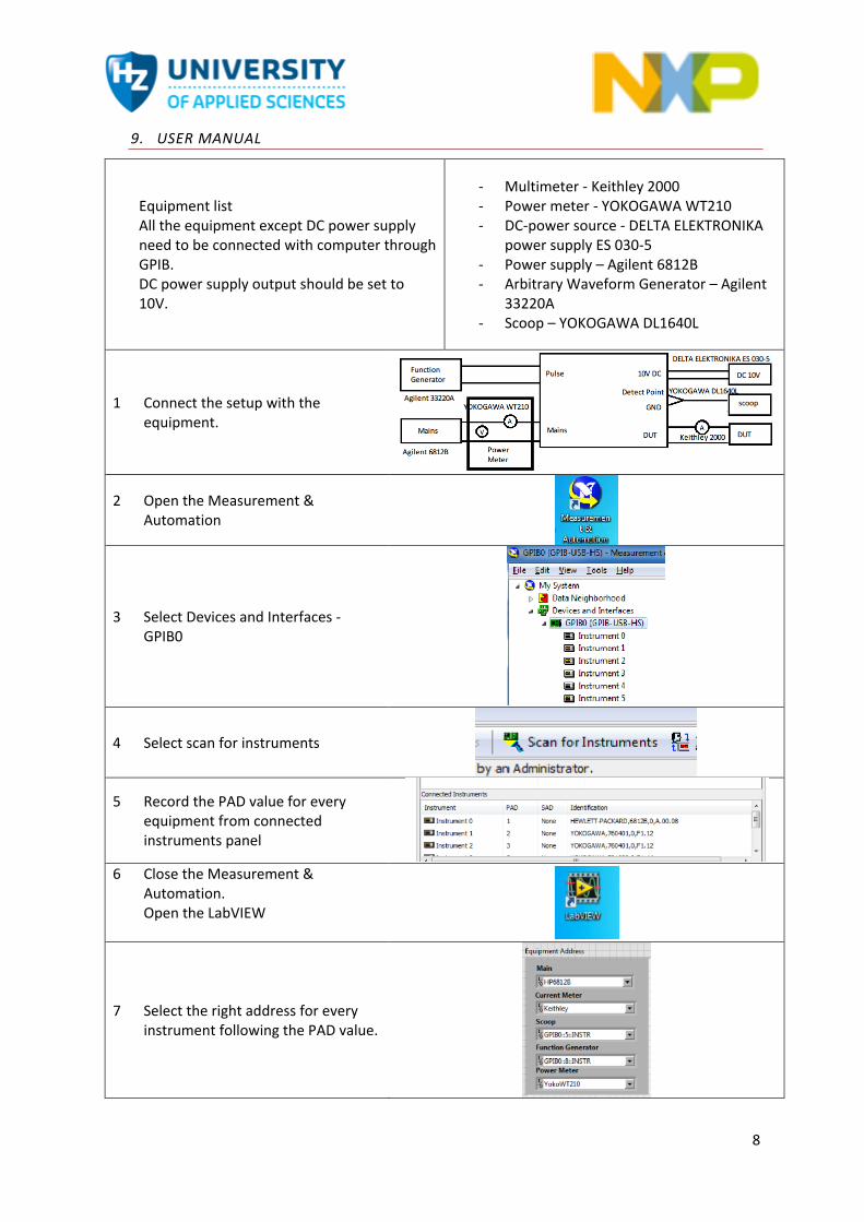
Equipment list All the equipment except DC power supply need to be connected with computer through GPIB. DC power supply output should be set to 10V.
- Multimeter - Keithley 2000 - Power meter - YOKOGAWA WT210 - DC-power source - DELTA ELEKTRONIKA
power supply ES 030-5 - Power supply – Agilent 6812B - Arbitrary Waveform Generator – Agilent
33220A - Scoop – YOKOGAWA DL1640L
1 Connect the setup with the equipment.
2 Open the Measurement & Automation
3 Select Devices and Interfaces - GPIB0
4 Select scan for instruments
5 Record the PAD value for every equipment from connected instruments panel
6 Close the Measurement &
Automation. Open the LabVIEW
7 Select the right address for every instrument following the PAD value.

9
8 Config the mains power supply
9 Set the test range and test step.
10 Click “Test“
11 If something is wrong, the error panel will show the information about the error.
12 When the setup is testing, the
status will be “testing”
13 After the test is over 14 Choose the sheet path and save
path
15 Click “Save”
16 The result will be saved into the excel file at the chosen path.