author's personal copy - university of exeter · author's personal copy superlattices and...
TRANSCRIPT

This article appeared in a journal published by Elsevier. The attachedcopy is furnished to the author for internal non-commercial researchand education use, including for instruction at the authors institution
and sharing with colleagues.
Other uses, including reproduction and distribution, or selling orlicensing copies, or posting to personal, institutional or third party
websites are prohibited.
In most cases authors are permitted to post their version of thearticle (e.g. in Word or Tex form) to their personal website orinstitutional repository. Authors requiring further information
regarding Elsevier’s archiving and manuscript policies areencouraged to visit:
http://www.elsevier.com/copyright

Author's personal copy
Superlattices and Microstructures 43 (2008) 399–407www.elsevier.com/locate/superlattices
Terahertz applications of carbon nanotubes
M.E. Portnoia,∗, O.V. Kibisb, M. Rosenau da Costac
a School of Physics, University of Exeter, Stocker Road, Exeter EX4 4QL, United Kingdomb Novosibirsk State Technical University, Novosibirsk 630092, Russia
c International Center for Condensed Matter Physics, 70904-970 Brasilia DF, Brazil
Available online 7 September 2007
Abstract
We formulate and justify several proposals utilizing unique electronic properties of carbon nanotubesfor a broad range of applications to THz optoelectronics, including THz generation by hot electrons inquasi-metallic nanotubes, frequency multiplication in chiral-nanotube-based superlattices controlled bya transverse electric field, and THz radiation detection and emission by armchair nanotubes in a strongmagnetic field.c© 2007 Elsevier Ltd. All rights reserved.
Keywords: Carbon nanotubes; Terahertz radiation
Creating a compact reliable source of terahertz (THz) radiation is one of the mostformidable tasks of contemporary applied physics [1]. One of the latest trends in THztechnology [2] is to use carbon nanotubes – cylindrical molecules with nanometer diameterand micrometer length [3–5] – as building blocks of novel high-frequency devices. Thereare several promising proposals of using carbon nanotubes for THz applications includinga nanoklystron utilizing extremely efficient high-field electron emission from nanotubes [2,6,7], devices based on negative differential conductivity in large-diameter semiconductingnanotubes [8,9], high-frequency resonant-tunneling diodes [10] and Schottky diodes [11–14],as well as electric field-controlled carbon nanotube superlattices [15], frequency multipliers [16,17], THz amplifiers [18], switches [19] and antennas [20].
In this paper we formulate and discuss several novel schemes to utilize the physical propertiesof single-wall carbon nanotubes (SWNTs) for generation and detection of THz radiation.
∗ Corresponding author.E-mail address: [email protected] (M.E. Portnoi).
0749-6036/$ - see front matter c© 2007 Elsevier Ltd. All rights reserved.doi:10.1016/j.spmi.2007.07.026

Author's personal copy
400 M.E. Portnoi et al. / Superlattices and Microstructures 43 (2008) 399–407
Fig. 1. (a) The scheme of THz photon generation by hot carriers in quasi-metallic SWNTs. (b) The spectral density ofspontaneous emission as a function of frequency for two values of applied voltage: solid line for V = 0.1 V; dashed linefor V = 0.15 V. The inset shows the directional radiation pattern of the THz emission with respect to the nanotube axis.
1. Quasi-metallic carbon nanotubes as terahertz emitters
This first scheme is based on the electric field-induced heating of electron gas in a nanotuberesulting in the inversion of population of optically active states with the energy differencewithin the THz spectrum range. It is well-known that the elastic backscattering processes inmetallic SWNTs are strongly suppressed [21], and in a high enough electric field charge carrierscan be accelerated up to the energy allowing emission of optical/zone-boundary phonons. Atthis energy, corresponding to the frequency of about 40 THz, the major scattering mechanismswitches on abruptly resulting in current saturation [22–26]. In what follows we show that forcertain types of carbon nanotubes the heating of electrons to the energies below the phonon-emission threshold results in the spontaneous THz emission with the peak frequency controlledby an applied voltage.
The electron energy spectrum of a metallic SWNT, ε(k), linearly depends on the electronwavevector k close to the Fermi energy and has the form ε(k) = ±hvF |k − k0|, wherevF ≈ 9.8×10⁵ m/s is the Fermi velocity of graphene, which corresponds to the commonly usedtight-binding matrix element γ0 = 3.033 eV [4,5]. Here and in what follows the zero of energyis defined as the Fermi energy position in the absence of an external field. When the voltage, V ,is applied between the SWNT ends, the electron distribution is shifted in the way shown by theheavy lines in Fig. 1(a) corresponds to the filled electron states. This shift results in inversionof population and, correspondingly, in optical transitions between filled states in the conductionband and empty states in the valence band. The spectrum of optical transitions is determinedby the distribution function for hot carriers, which in turn depends on the applied voltage andscattering processes in the SWNT. It is well-known that the major scattering mechanism inSWNTs is due to electron–phonon interaction [22–24,26]. Since the scattering processes erodethe inversion of electron population, an optimal condition for observing the discussed opticaltransitions takes place when the length of the SWNT L < lac, where the electron mean-freepath for acoustic phonon scattering is lac ≈ 2 µm [24]. Below we consider only such shortSWNTs with ideal Ohmic contacts [23] and in the ballistic transport regime, when the energyacquired by the electron on the whole length of the tube, 1ε = eV, does not exceed the value of

Author's personal copy
M.E. Portnoi et al. / Superlattices and Microstructures 43 (2008) 399–407 401
hΩ = 0.16 eV at which the fast emission of high-energy phonons begins [24]. In this so-calledlow-bias regime [22–24], in which the current in the nanotube is given by the Buttiker–Landauer-type formula, I ≈ (4e2/h)V , the distribution function of hot electrons is
fe(k) =
1, 0 < k − k0 < 1ε/2hvF0, k − k0 > 1ε/2hvF .
(1)
The distribution function for hot holes, fh(k), has the same form as that of fe(k).Let us select a SWNT with the crystal structure most suitable for observation of the discussed
effect. First, the required nanotube should have metallic conductivity and, second, the opticaltransitions between the lowest conduction subband and the top valence subband should beallowed. The crystal structure of a SWNT is described by two integers (n, m), which completelydefine its physical properties [3–5]. SWNTs with true metallic band structure, for which theenergy gap is absent for any SWNT radius, are armchair (n, n) SWNTs only [5,27–30]. However,for armchair SWNTs the optical transitions between the first conduction and valence subbandsare forbidden [31,32]. So we propose to use for the observation of THz generation the so-calledquasi-metallic (n, m) SWNTs with n −m = 3p, where p is a non-zero integer. These nanotubes,which are gapless within the frame of a simple zone-folding model of the π -electron graphenespectrum [4], are in fact narrow-gap semiconductors due to curvature effects. Their bandgap isgiven by εg = hvF aC–C cos 3θ/(8R2) [27,30], where aC–C = 1.42 A is the nearest-neighbordistance between two carbon atoms, R is the nanotube radius, and θ = arctan[
√3m/(2n + m)]
is the chiral angle [4]. It can be seen from the expression for εg that the gap is decreasing rapidlywith increase in the nanotube radius. For large values of R, this gap can be neglected even inthe case of moderately applied voltages due to Zener tunneling of electrons across the gap. It iseasy to show in the fashion similar to that of the original Zener’s work [33] that the tunnelingprobability in quasi-metallic SWNTs is given by exp(−αε2
g/eEhvF ), where α is a numericalfactor close to unity [34]. For example, for a zigzag (30, 0) SWNT the gap is εg ≈ 6 meVand the Zener breakdown takes place for the electric field E ∼ 10−1 V/µm. Since almost thewhole voltage drop in the ballistic regime occurs within the few-nanometer regions near thecontacts [35] a typical bias voltage of 0.1 V corresponds to an electric field, which is more thansufficient to achieve a complete breakdown. In what follows, all our calculations are performedfor a zigzag (3p, 0) SWNT of large enough radius R and for applied voltages exceeding theZener breakdown, so that the finite-gap effects can be neglected. The obtained results can beeasily generalized for any quasi-metallic large-radius SWNT.
Optical transitions in SWNTs have been a subject of extensive research (see, e.g., Refs. [31,32,36–40]). We treat these transitions using the results of the nearest-neighbor orthogonal π -electrontight-binding model [4]. Despite its apparent simplicity and well-known limitations, this modelhas been extremely successful in describing low-energy optical spectra and electronic propertiesof SWNTs (see, e.g., Ref. [41] for one of the most recent manifestations of this model success).Our goal is to calculate the spectral density of spontaneous emission, Iν , which is the probabilityof optical transitions per unit time for the photon frequencies in the interval (ν, ν + dν) dividedby dν. In the dipole approximation [42] this spectral density is given by
Iν =8πe2ν
3c3
∑i, f
fe(ki ) fh(k f )∣∣⟨Ψ f
∣∣vz∣∣Ψi
⟩∣∣2δ(εi − ε f − hν). (2)
Eq. (2) contains the matrix element of the electron velocity operator. In the frame of the tight-binding model, this matrix element for optical transitions between the lowest conduction and thehighest valence subbands of the (3p, 0) zigzag SWNT can be written as (cf. Ref. [32,36])

Author's personal copy
402 M.E. Portnoi et al. / Superlattices and Microstructures 43 (2008) 399–407⟨Ψ f
∣∣vz∣∣Ψi
⟩=
aC–Cωi f
8δk f ,ki , (3)
where hωi f = εi − ε f is the energy difference between the initial (i) and the final ( f ) states.These transitions are associated with the light polarized along the nanotube axis z, in agreementwith the general selection rules for SWNTs [31]. Substituting Eq. (3) in Eq. (2) and performingthe necessary summation, we get
Iν = L fe(πν/vF ) fh(πν/vF )π2e2a2
C–Cν3
6c3hvF. (4)
Eq. (4) has broader applicability limits than the considered case of L < lac and eV < hΩ ,in which the distribution functions for electrons and holes are given by Eq. (1). In the generalcase there is a strong dependence of Iν on the distribution functions, which have to be calculatedtaking into account all the relevant scattering mechanisms [22–24,26]. In the discussed ballisticregime the spectral density has a universal dependence on the applied voltage and photonfrequency for all quasi-metallic SWNTs. In Fig. 1(b) the spectral density is shown for two valuesof the voltage. It is clearly seen that the maximum of the spectral density of emission has strongvoltage dependence and lies in the THz frequency range for experimentally attainable voltages.The directional radiation pattern, shown in the inset of Fig. 1(b), reflects the fact that emissionof light polarized normally to the nanotube axis is forbidden by the selection rules for the opticaltransitions between the lowest conduction subband and the top valence subband.
For some device applications it might be desirable to emit photons propagating along thenanotube axis, which is possible in optical transitions between the SWNT subbands characterizedby angular momenta differing by one [5,31]. To achieve the emission of these photons by theelectron heating, it is necessary to have an intersection of such subbands within the energy rangeaccessible to electrons accelerated by attainable voltages. From our analysis of different types ofSWNTs, it follows that the intersection is possible, e.g., for the lowest conduction subbandsin several semiconducting zigzag nanotubes and in all armchair nanotubes. However, for aneffective THz emission from these nanotubes it is necessary to move the Fermi level very closeto the subband intersection point [43]. Therefore, obtaining the THz emission propagating alongthe nanotube axis is a more difficult technological problem than generating emission as shownin Fig. 1(b).
2. Chiral carbon nanotubes as frequency multipliers
Another proposal for using SWNTs for THz applications is based on chiral nanotubes, whichrepresent natural superlattices. For example, a (10, 9) single-wall nanotube has a radius whichdiffers from the radius of the most commonly studied (10, 10) nanotube by less than five percent, whereas a translational period T along the axis of the (10, 9) SWNT is almost thirty timeslarger than the period of the (10, 10) nanotube. Correspondingly, the first Brillouin zone of the(10, 9) nanotube is thirty times smaller than the first zone for the (10, 10) tube. However sucha Brillouin zone reduction cannot influence electronic transport unless there is a gap openingbetween the energy subbands resulting from the folding of graphene spectrum. In our researchwe show how an electric field normal to the nanotube axis opens noticeable gaps at the edge ofthe reduced Brillouin zone, thus turning a long-period nanotube of certain chirality into a ‘real’superlattice. The field-induced gaps are most pronounced in (n, 1) SWNTs [15,44]. Fig. 2(a)shows the opening of electric field-induced gap near the edge of the Brillouin zone of a (6, 1)
SWNT. This gap opening results in the appearance of a negative effective-mass region in the

Author's personal copy
M.E. Portnoi et al. / Superlattices and Microstructures 43 (2008) 399–407 403
Fig. 2. (a) Energy spectrum of the (6, 1) SWNT in a transverse electric field, E⊥ = 4 V/nm. (b) The electron driftvelocity in the lowest conduction subband of a (6, 1) SWNT as a function of the longitudinal electric field, in the presenceof acoustic-phonon scattering.
Fig. 3. Time dependence of the electron velocity in the lowest conduction subband of a (6, 1) SWNT under the influenceof a pump harmonic longitudinal electric field, E‖ (t) = E0 sin (ω0t), and its corresponding spectral distribution A (ω):
(a) in the ballistic transport regime; (b) in the presence of scattering with the relaxation time τ = 10−12 s.
nanotube energy spectrum. The typical electron energy in this part of the spectrum of 15 meVis well below the optical phonon energy hΩ ≈ 160 meV, so that it can be easily accessed inmoderate heating electric fields. The negative effective mass results in the negative differentialconductivity (NDC), as can be seen from Fig. 2(b). The effect of the negative effective mass alsoleads to an efficient frequency multiplication in the THz range. The results of our calculationsof the electron velocity in the presence of the time-dependent longitudinal electric field arepresented in Fig. 3. One of the advantages of a frequency multiplier based on chiral SWNTs, in
Author's personal copy
404 M.E. Portnoi et al. / Superlattices and Microstructures 43 (2008) 399–407
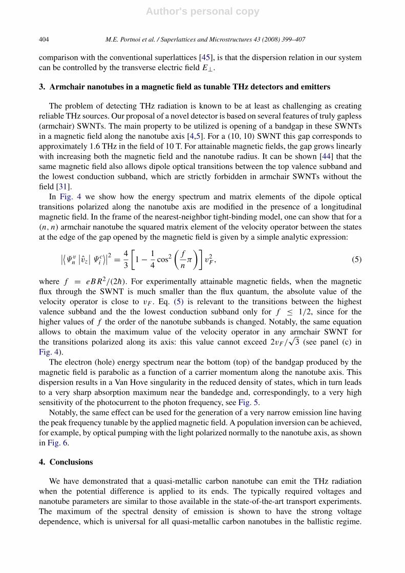
comparison with the conventional superlattices [45], is that the dispersion relation in our systemcan be controlled by the transverse electric field E⊥.
3. Armchair nanotubes in a magnetic field as tunable THz detectors and emitters
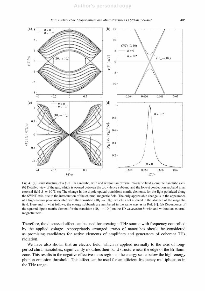
The problem of detecting THz radiation is known to be at least as challenging as creatingreliable THz sources. Our proposal of a novel detector is based on several features of truly gapless(armchair) SWNTs. The main property to be utilized is opening of a bandgap in these SWNTsin a magnetic field along the nanotube axis [4,5]. For a (10, 10) SWNT this gap corresponds toapproximately 1.6 THz in the field of 10 T. For attainable magnetic fields, the gap grows linearlywith increasing both the magnetic field and the nanotube radius. It can be shown [44] that thesame magnetic field also allows dipole optical transitions between the top valence subband andthe lowest conduction subband, which are strictly forbidden in armchair SWNTs without thefield [31].
In Fig. 4 we show how the energy spectrum and matrix elements of the dipole opticaltransitions polarized along the nanotube axis are modified in the presence of a longitudinalmagnetic field. In the frame of the nearest-neighbor tight-binding model, one can show that for a(n, n) armchair nanotube the squared matrix element of the velocity operator between the statesat the edge of the gap opened by the magnetic field is given by a simple analytic expression:∣∣⟨Ψv
n
∣∣vz∣∣Ψ c
i
⟩∣∣2=
43
[1 −
14
cos2(
f
nπ
)]v2
F , (5)
where f = eB R2/(2h). For experimentally attainable magnetic fields, when the magneticflux through the SWNT is much smaller than the flux quantum, the absolute value of thevelocity operator is close to vF . Eq. (5) is relevant to the transitions between the highestvalence subband and the the lowest conduction subband only for f ≤ 1/2, since for thehigher values of f the order of the nanotube subbands is changed. Notably, the same equationallows to obtain the maximum value of the velocity operator in any armchair SWNT forthe transitions polarized along its axis: this value cannot exceed 2vF/
√3 (see panel (c) in
Fig. 4).The electron (hole) energy spectrum near the bottom (top) of the bandgap produced by the
magnetic field is parabolic as a function of a carrier momentum along the nanotube axis. Thisdispersion results in a Van Hove singularity in the reduced density of states, which in turn leadsto a very sharp absorption maximum near the bandedge and, correspondingly, to a very highsensitivity of the photocurrent to the photon frequency, see Fig. 5.
Notably, the same effect can be used for the generation of a very narrow emission line havingthe peak frequency tunable by the applied magnetic field. A population inversion can be achieved,for example, by optical pumping with the light polarized normally to the nanotube axis, as shownin Fig. 6.
4. Conclusions
We have demonstrated that a quasi-metallic carbon nanotube can emit the THz radiationwhen the potential difference is applied to its ends. The typically required voltages andnanotube parameters are similar to those available in the state-of-the-art transport experiments.The maximum of the spectral density of emission is shown to have the strong voltagedependence, which is universal for all quasi-metallic carbon nanotubes in the ballistic regime.
Author's personal copy
M.E. Portnoi et al. / Superlattices and Microstructures 43 (2008) 399–407 405
Fig. 4. (a) Band structure of a (10, 10) nanotube, with and without an external magnetic field along the nanotube axis.(b) Detailed view of the gap, which is opened between the top valence subband and the lowest conduction subband in anexternal field B = 10 T. (c) The change in the dipole optical transitions matrix elements, for the light polarized alongthe SWNT axis, due to the introduction of the external magnetic field. The only appreciable change is in the appearanceof a high-narrow peak associated with the transition (10v → 10c), which is not allowed in the absence of the magneticfield. Here and in what follows, the energy subbands are numbered in the same way as in Ref. [4]. (d) Dependence ofthe squared dipole matrix element for the transition (10v → 10c) on the 1D wavevector k, with and without an externalmagnetic field.
Therefore, the discussed effect can be used for creating a THz source with frequency controlledby the applied voltage. Appropriately arranged arrays of nanotubes should be consideredas promising candidates for active elements of amplifiers and generators of coherent THzradiation.
We have also shown that an electric field, which is applied normally to the axis of long-period chiral nanotubes, significantly modifies their band structure near the edge of the Brillouinzone. This results in the negative effective-mass region at the energy scale below the high-energyphonon-emission threshold. This effect can be used for an efficient frequency multiplication inthe THz range.

Author's personal copy
406 M.E. Portnoi et al. / Superlattices and Microstructures 43 (2008) 399–407
Fig. 5. (a) Calculated photon absorption spectra for a (10, 10) SWNT, for three different magnetic field values. The
absorption intensity is proportional to the product of∣∣⟨Ψv
10
∣∣ vz∣∣Ψc
10⟩∣∣2 and the joint density of states. (b) Dependence of
the position of the peak in the absorption intensity, associated with the Van Hove singularity, on the magnetic field.
Fig. 6. A scheme for creating a population inversion between the lowest conduction subband and the top valence subbandof an armchair SWNT in a magnetic field. The left plot shows the calculated matrix elements of the relevant dipole opticaltransitions polarized normally to the axis of a (10, 10) SWNT. The right plot shows several energy subbands closest tothe Fermi level and illustrates the creation of photoexcited carriers and their non-radiative thermalization.
Finally, we have discussed the feasibility of using the effect of the magnetic field, whichopens energygaps and allows optical transitions in armchair nanotubes, for creating tunable THzdetectors and emitters.
Acknowledgments
This research was supported by the EU Foundation INTAS (Grants 03-50-4409 and 05-1000008-7801), the Russian Foundation for Basic Research (Grants 08-02-90004, 06-02-16005and 06-02-81012), the Russian Ministry for Education and Science (Grant RNP.2.1.1.1604), andthe Royal Society (UK), MCT and FINEP (Brazil).
References
[1] B. Ferguson, X.C. Zhang, Nat. Mater. 1 (2002) 26.[2] D. Dragoman, M. Dragoman, Progr. Quantum Electron. 28 (2004) 1.[3] S. Iijima, Nature 354 (1991) 56.[4] R. Saito, G. Dresselhaus, M.S. Dresselhaus, Physical Properties of Carbon Nanotubes, Imperial College Press,
London, 1998.

Author's personal copy
M.E. Portnoi et al. / Superlattices and Microstructures 43 (2008) 399–407 407
[5] S. Reich, C. Thomsen, J. Maultzsch, Carbon Nanotubes: Basic Concepts and Physical Properties, Wiley, Berlin,2004.
[6] H.M. Manohara, et al., J. Vac. Sci. Technol. B 23 (2005) 157.[7] A. Di Carlo, et al., Proc. SPIE 6328 (2006) 632808.[8] A.S. Maksimenko, G.Ya. Slepyan, Phys. Rev. Lett. 84 (2000) 362.[9] G. Pennington, N. Goldsman, Phys. Rev. B 68 (2003) 045426.
[10] D. Dragoman, M. Dragoman, Physica E 24 (2004) 282.[11] A.A. Odintsov, Phys. Rev. Lett. 85 (2000) 150.[12] F. Leonard, J. Tersoff, Phys. Rev. Lett. 85 (2000) 4767.[13] M.H. Yang, et al., Appl. Phys. Lett. 87 (2005) 253116.[14] C. Lu, et al., Appl. Phys. Lett. 88 (2006) 133501.[15] O.V. Kibis, D.G.W. Parfitt, M.E. Portnoi, Phys. Rev. B 71 (2005) 035411.[16] G.Ya. Slepyan, et al., Phys. Rev. A 60 (1999) 777.[17] G.Ya. Slepyan, et al., Phys. Rev. A 63 (2001) 053808.[18] D. Dragoman, M. Dragoman, Physica E 25 (2005) 492.[19] M. Dragoman, et al., Appl. Phys. Lett 88 (2006) 073503.[20] G.Ya. Slepyan, et al., Phys. Rev. B 73 (2006) 195416.[21] T. Ando, T. Nakanishi, R. Saito, J. Phys. Soc. Jpn. 67 (1997) 1704.[22] Z. Yao, C.L. Kane, C. Dekker, Phys. Rev. Lett. 84 (2000) 2941–2944.[23] A. Javey, et al., Phys. Rev. Lett. 92 (2004) 106804.[24] J.-Y. Park, et al., Nano Lett. 4 (2004) 517.[25] M. Freitag, et al., Nano Lett. 4 (2004) 1063.[26] V. Perebeinos, J. Tersoff, P. Avouris, Phys. Rev. Lett. 94 (2005) 086802.[27] C.L. Kane, E.J. Mele, Phys. Rev. Lett. 78 (1997) 1932.[28] M. Ouyang, et al., Science 292 (2001) 702.[29] Y. Li, U. Ravaioli, S.V. Rotkin, Phys. Rev. B 73 (2006) 035415.[30] D. Gunlycke, et al., Europhys. Lett. 73 (2006) 759.[31] I. Milosevic, et al., Phys. Rev. B 67 (2003) 165418.[32] J. Jiang, et al., Carbon 42 (2004) 3169.[33] C. Zener, Proc. Royal. Soc. (London) 145 (1934) 523.[34] For the energy spectrum near the band edge given by ε = ±[ε2
g/4 + h2 v2F (k − k0)2
]1/2, it can be shown that
α = π/4.[35] A. Svizhenko, M.P. Anantram, Phys. Rev. B 72 (2005) 085430.[36] A. Gruneis, et al., Phys. Rev. B 67 (2003) 165402.[37] V.N. Popov, L. Henrard, Phys. Rev. B 70 (2004) 115407.[38] R. Saito, et al., Appl. Phys. A 78 (2004) 1099.[39] S.V. Goupalov, Phys. Rev. B 72 (2005) 195403.[40] Y. Oyama, et al., Carbon 44 (2006) 873.[41] M.Y. Sfeir, et al., Science 312 (2006) 554.[42] V.B. Berestetskii, E.M. Lifshitz, L.P. Pitaevskii, Quantum Electrodynamics, Butterworth-Heinemann, Oxford, 1997.[43] O.V. Kibis, M.E. Portnoi, Technical Phys. Lett. 31 (2005) 671.[44] M. Rosenau da Costa, O.V. Kibis, M.E. Portnoi (in press).[45] K.N. Alekseev, et al., Europhys. Lett. 73 (2006) 934.