author/filing title
TRANSCRIPT

' /
Pllklngton Library
I • Loughborough ., University
Author/Filing Title .......• ~~-~ .. /. ..•. ) .....••........•..•........•.•...•.
·····························•···································································· Accession/Copy No. £l'to I 6 o & '2-~
Vol. No. .•...•.......... Class Mark .............................................. ..


Photoemission Studies of Intermetallic Compounds
by
David Brown
A Doctoral Thesis Submitted in Partial Fulfilment of the Requirements for
the Award of Doctor of Philosophy at Loughborough University.
September 1997
"'( ....... "·'r"",·,-,.,.,.--, ............ _.,_
'.,_ '
· © David Brown(l997)


Abstract
1. Introduction
I . I Overview
1.2 Electronic Structure of Metals
Contents
1.3 Photoemission from Metals and Alloys
2. Heusler and Cu3Au-Type Intermetallic Compounds
Page Number:
3
8
2.1 Structure and Properties of X2Mn Y Alloys 13
2.2 Structure and Properties of Pd2TiY Alloys 16
2.3 Structure and Properties of Pt3Z Alloys 18
2.4 Summary 21
3. Principles of the Experimental Techniques
3.1 Auger Electron Spectroscopy (AES) 22
3.2 Ultraviolet Photoemission Spectroscopy (UPS) 24
3.3 Photoionisation Cross-Sections and the Cooper Minimum 28
3.4 Valence Band Spectra of Intermetallic Compounds 32
3.5 Resonant Photoemission 34
4. Experimental Details
4.1 The Synchrotron Radiation Source (SRS) 38
4.2 SRS Beamlines 6.1 and 6.2 39
4.3 AES and UPS Measurements on the Alloy Systems 41
4.4 Data Analysis 43

5. Results and Discussion for XzMnY Alloys
5.1 Determination of Surface Composition by AES
5.2 Non-Resonant Photoemission
5.3 Comparison with Band-Structure Calculations
5.4 Resonant Photoemission
5.5 Summary
6. Results and Discussion for PdzTiY Alloys
6.1 Determination of Surface Composition by AES
6.2 Cooper Minimum Studies
6.3 Resonant Photoemission
6.4 Comparison with Band-Structure Calculations
6.5 Summary
7. Results and Discussion for Pt3Z Alloys
48
49
51
59
67
69
69
73
75
78
7 .I Determination of Surface Composition by AES 79
7.2 Cooper Minimum Studies 80
7.3 Resonant Photoemission 82
7.4 Experimental Determination of the Partial Density of States 86
7.5 Summary 90
8. Final Summary and Conclusions
8.1 Conclusions for X2MnY Alloys 91
8.2 Conclusions for Pd2TiY Alloys 93
8.3 Conclusions for Pt3Z Alloys 95
8.4 Final Remarks 96
References
ii

Acknowledgements
Most experimental research requires a team effort and the work described in this thesis is no
exception. Financial support was provided by Loughborough University and through the EPSRC minor
grants scheme for Daresbury Laboratory. The alloy samples were supplied by the Condensed Matter
Group at Loughborough and in this regard I am indebted to Professor Kurt Ziebeck, Bharat "Chas"
Chavda, Nadum Zayer and Ahmad Bargawi. Pat Newman spark eroded the samples with great care and
sometimes at short notice. Photoemission spectra were compared with theoretical hand-structure
calculations performed by other workers. I am grateful to all the authors who kindly gave their permission
to reproduce data. The original authors have, of course, been acknowledged in the main body of the text
and in the captions to the figures. I would also like to thank Dr. Mike Petty for digitising published figures
with the "Datathief' software package. Because of persuasion, coercion or blackmail, many members of
the Physics Department have given up their time to assist me at Daresbury. These include Karen Bedwell,
Martin Butterfield, Mike Crapper, Lorraine Flannery, Steve Guilfoyle, Andy Malins, Mike Petty, Paul
Skull, Jacqui Smith and Neil Telling. Thanks to you all. In addition, Stuart Downes and Dave Teehan
have provided excellent technical support at Daresbury SRS. Above all, thanks are due to my supervisor,
Dr. Mike Crapper, for giving me an opportunity to work with him and for providing constant
encouragement and guidance throughout. It has been a pleasure and a privilege to work with him over the
past three years. Last, but by no means least, I would like to thank my parents for their support and
encouragement throughout my career.
iii

Abstract
Ultraviolet photoemission spectroscopy has been employed to investigate the electronic
density of states of Heusler and Cu3Au-type intermetallic compounds. Cooper minima and
resonant photoemission effects have been utilised to determine the contribution of the
constituent elements to the valence band spectra. For the Mn-based Heusler alloys Co2MnSn,
Cu2MnAl and Pd2MnSn, the Mn 3d-derived states disperse across the full width of the valence
band. The total bandwidth increases from 5 eV in the case of Co2MnSn, to 7 eV for Pd2MnSn.
Differences in resonant structure are evident across the band for Co2MnSn. This may reflect a
variation in initial state hybridisation, with Mn 3d states at the bottom of the band more
localised than the corresponding states closer to the Fermi level. Photoemission measurements
on the Ti-based Heusler alloys Pd2TiAl, Pd2Tiln and Pd2TiSn indicate that the bandwidth is
approximately 7-8 e V in each case. The Pd 4d electronic contribution dominates at a binding
energy of approximately 3 eV, whilst Ti 3d states contribute most strongly immediately below
the Fermi level. The Cu3Au-type alloys Pt3 V and Pt3Mn possess valence band-structure
extending up to 8 eV below the Fermi level. The Pt 5d and transition metal 3d states completely
overlap in each case. The concentration of 3d states in Pt3 V is greatest immediately below the
Fermi level, but Mn 3d states in Pt3Mn contribute most strongly at a binding energy of 2.6 eV.
For each of the Heusler and Cu3Au-type alloys investigated, the experimental photoemission
spectra have been compared with simulated spectra derived from theoretical band-structure
calculations. The results are discussed in the context of competing models for local moment
formation in these materials.
iv

11 1. Introduction
1.1 Overview
Intermetallic compounds of the ternary Heusler and binary Cu3Au-type have been
widely studied experimentally [1-15] and theoretically [16-30]. They provide model
systems for the investigation of ordering and are useful in the evaluation of energy-band
calculation schemes. Heusler alloys of general composition X2MnY (X = Co, Ni, Cu,
Pd; Y =AI, In, Sn, Sb) and Cu3Au-type alloys of composition Pt3Z (Z = Ti, V, Cr, Mn,
Fe, Co) are of particular interest, since in most cases these alloys also exhibit magnetic
ordering. It is generally accepted that these materials are ideal models for the
investigation of local moment behaviour. For the case of the Mn-based Heusler alloys, a
moment of approximately 4 l-Is is associated with the Mn sub-lattice [2]. When X = Co
or Ni, an additional moment is also associated with the X atom sites [3]. For the Pt3Z
series, with the exception of Pt3Ti, a local moment is associated with the first-row
transition metal. Smaller moments may also be associated with the Pt sites to give an
overall ferro- or ferrimagnetic arrangement [12, 13].
The traditional description for such local moment systems is in terms of virtual
bound, localised states similar to those described for dilute alloys [3 I, 32]. However,
more recent band-structure calculations for the X2MnY alloys appear to contradict this
model and suggest that the Mn 3d states form a strongly hybridised, delocalised band
with the X atom d states [16-20]. The local moment is considered to result, not from
localisation of the Mn 3d states, but from exclusion of minority-spin electrons from Mn
sites. The localised moments, therefore, result from completely itinerant electrons.
Corresponding calculations for the Pt3Z alloys show similar hybridisation between the
Pt and Z atom d states [30].
Recent additions to the Heusler family are the Ti-based alloys of composition
Pd2TiY (Y =AI, In, Sn) [5-7]. Since the Ti-Ti separation in the crystal lattice is similar
11
to the Mn-Mn separation in the Pd2Mn Y (Y = In, Sn) alloys, it might be expected that
these materials also form local moment systems. However, although magnetic ordering
has been reported for all 3 alloys, the magnetic properties cannot readily be explained by
current models of localised or itinerant behaviour. Band-structure calculations do not
reveal the origin of the magnetism, but instead indicate that the Pd2TiY alloys should be
paramagnetic [21-23].
It is apparent that, in order to obtain a fundamental understanding of the mechanism
by which the local moments are formed in these materials, a detailed description of the
electronic structure is a necessary prerequisite. However, there have been comparatively
few attempts to elucidate the valence band-structures by direct experimental methods.
The scarcity of experimental data has hampered attempts to model the magnetic
properties. The aim of the research described in this thesis, therefore, has been to
systematically investigate the valence bands of Heusler and Cu3Au-type alloys using
ultraviolet photoemission spectroscopy. Polycrystalline ingots of the intermetallic
compounds Co2MnSn, Cu2MnAl, Pd2MnSn, Pd2TiAl, Pd2Tiln, Pd2TiSn, Pt3V and
Pt3Mn have all been studied.
Utilising the tunable radiation associated with a synchrotron source, it is possible to
obtain information on the contribution of the constituent elements to the valence band
by means of Cooper minima and resonance effects [33-37]. For orbitals with a radial
node in the wavefunction, the cancellation of matrix element integrals for transitions to
particular final states results in a minimum in the photoionisation cross-section. This
minimum, originally predicted by Cooper [33], has been extensively used to determine
the partial densities of states for alloys comprising 4d or 5d metals such as Pd, Pt or Au
[8, 34]. For 3d metals, at photon energies corresponding to the 3p threshold, there is an
enhancement in the emission from the 3d band resulting from p-to-d transitions [35-37].
This results in a characteristic modulation in the photocurrent arising from regions of
the valence band possessing significant 3d character.
In view of the contentious nature of the origin of magnetic ordering in Pd2TiY alloys
and the disparity between the theoretical models for local moment formation in X2MnY
and Pt3Z alloys, the methods outlined above have been employed in an attempt to
2

address these issues. By comparing experimental photoemission measurements with
calculations of the electronic structure, an attempt has been made to validate the theory.
In particular, the extent of hybridisation of the d states associated with the local
moments has been investigated.
The thesis has been organised into 8 main sections. The current section provides a
brief introduction to the aims of the research and attempts to provide some context with
respect to the available literature. Section 2 describes the crystallographic and magnetic
properties of the alloys under investigation and presents some typical theoretical
calculations of the corresponding band-structures. The physical principles of the
experimental techniques employed are outlined in section 3, together with details of
how the techniques may be applied to the current investigation. Section 4 deals with the
practical aspects of the research, including details of the synchrotron source and
associated photoemission beamlines. Manipulation and analysis of the raw data is also
discussed. Results obtained for the X2Mn Y, Pd2TiY and Pt3Z alloys are presented in
sections 5-7 respectively. Each section gives details of the results obtained from Auger
electron spectroscopy and ultraviolet photoemission, including Cooper minima and
resonance effects. The experimental results are compared with calculated band
structures from the literature. A short summary of the research is provided at the end of
each of the sections 5-7. Finally, section 8 draws together the results from all the
intermetallic compounds investigated and discusses the extent to which the research
objectives have been accomplished. Possibilities for further work are also considered.
1.2 Electronic Structure of Metals
One of the earliest theoretical models describing the electronic structure in metals
was proposed by Drude in 1900 [38, 39]. According to the Drude model, when atoms of
a metallic element condense to form a metal, the core electrons remain bound to the
nucleus to form a metallic ion. The valence electrons, however, become detached and
move freely throughout the metal, forrning a free electron "gas". Drude applied kinetic
3

theory to this free electron "gas", assuming that collisions occur between the mobile
electrons and stationary ion cores. Between collisions, electron-electron and electron-ion
interactions are neglected. This is the basis of the independent electron and free electron
approximations respectively. The classical free electron model of Drude was later
modified by Sommerfeld [40] to include the application of Fermi-Dirac statistics and
forms the basis for the quantised free electron theory. In this theory, the one-electron
Schri:idinger equation is given by
[ -!!_V'' + V(r)l,(r) 2m J"' Eljl (r) ( 1.1 ),
where 'l'(r) is an electronic wavefunction associated with an energy level, E, and the
potential, V(r), is taken to be zero. All other symbols have their usual meanings. The
confinement of the electron to the metal, considered by mathematical convention to be a
cube of side L, can be represented by imposition of the periodic boundary condition
ljl(x+L,y+L,z+L) = ljl(x,y,z) (1.2).
A solution of the Schrtidinger equation ( 1.1) is provided by a plane wave possessing a
wave vector, k, so that
I
ljl ,(r) = ( ~' )' exp{ik.r) (1.3).
The normalisation constant arises from the condition
x=L 1·=L :.=L
J J Jljl'(x,y.z)ljl(x,y.z)dxdydz = (1.4), .("() y=U :=0
which assumes that the probability of locating the electron somewhere within the cube is
unity. The associated energy is described by
4

E(k) = n' [k' + k' + k' J = 2nz X .I •
(1.5).
The boundary condition ( 1.2) permits only certain discrete values of k , where the
components must take the form
2n:n1 =- k = L '
~ L
( 1.6),
with nx, n, and n, integers. The density of states, D(E), can be defined such that
D(E)dE corresponds to the number of states in the energy interval between E and
E +dE per unit volume. For free electrons, the relationship between electron energy
and density of electron states has a parabolic form,
D(E) .1 I
= _I (2m)2 E'i 2"' n'
(1.7).
The occupancy of a state with energy, E, is determined by the Fermi-Dirac distribution,
f(E), where
/(E) = ( 1.8).
(E-E) l+exp --'
k,T
The Fermi level, EF, represents the energy boundary between occupied and unoccupied
electronic states. The form of the Fermi-Dirac distribution is such that when E = EF,
f(E) = 0.5. At T =OK, f(E) is a step function. However, at higher temperatures, the
occupation of states in the region close to E F becomes "smeared out", with a small
number of states just below EF unoccupied and the same number of states just above
EF occupied. From equations (1.7) and (1.8}, the total number of occupied electronic
states, N, can be established from the relationship
N = f D(E)f(E)dE (1.9).
5

A more rigorous approach requires a consideration of a non-zero potential energy. If
the crystal is perfectly periodic, the effective one-electron potential is considered to have
the periodicity of the underlying lattice. The potential must, therefore, satisfy the
condition
V(r) = V(r+ R) where R = n1a 1 + n,a, + n,a, ( 1.1 0).
R represents an arbitrary translation vector of the 3-dimensional periodic lattice and
consists of integer multiples 111 , n2 , n3 of the 3 basis vectors a,, a2 , a 3 of the real
space lattice. According to the description of Bloch [41], wavefunctions subject to such
a potential are assumed to possess the characteristics of a plane wave multiplied by a
function with the same periodicity as the crystal lattice,
IJ1 ,,(r) = u,,(r)exp(ik.r) where u,,(r) = u,,(r+ R) (1.11).
The principal consequence of applying a periodic potential is the formation of
separate energy bands, denoted by the band index, 11. Wavefunctions constructed from
real values of k are only possible within certain allowed energy bands. Such "band"
electrons are described by wavefunctions that extend without attenuation through the
crystal. Assuming perfect periodicity, electrons are not scattered by the array of ion
cores as predicted by classical theory, but possess an infinite mean free path. Scattering
only occurs when the periodicity is interrupted. Wavefunctions with imaginary k,
however, cannot move freely through the crystal. This results in the formation of regions
of forbidden energy for mobile electrons in the solid. The only wavefunctions that are
valid in the forbidden gap are "bound" states localised around defects in the lattice.
The wave vector, k, can always be confined to the first Brillouin zone, or any other
primitive cell of the reciprocal lattice, by the relationship
k* = k+G (1.12).
6

k and k * represent wave vectors that lie inside and outside the first zone respectively
and G is a reciprocal lattice vector. For a given band, n, the set of all wavefunctions
and energy levels for values of k differing by a reciprocal lattice vector, G , are
identical. This is represented by the relationships
1jl,,(r) = '1',_,.0 (r) and E,(k) = E,(k+G) (1.13).
The energy levels of an electron in a periodic potential can, therefore, be described in
terms of a family of continuous functions, E, (k) , each possessing the same periodicity
as the reciprocal lattice. The information contained within these functions is described
as the band-structure of the solid. The DOS is obtained by integration over an energy
shell between E(k) and E(k) +dE ink-space. The free electron DOS has already been
given in equation (1.7), but a more general relationship between the DOS and the band-
structure is
D,(E) =-1 f dS 41t' s,, <£> JV E, (k)j
where S,(E) is a surface of constant energy.
(1.14).
Energy bands in solids are often described within the framework of the tight-binding
(TB) model [42, 43]. A system of widely separated atoms has many degenerate electron
states. If the interatomic spacing is decreased to the equilibrium spacing in the solid,
interatomic coupling causes the initially degenerate atomic levels to disperse across a
range of energies. Each resulting band accomodates the same number of states as were
originally available in the atomic levels. The dispersion, or bandwidth, is dependent on
the degree of overlap between the interacting orbitals. Since core level wavefunctions do
not extend as far from the nucleus as valence wavefunctions, it is the valence states that
overlap most strongly and thereby exhibit strong dispersion. The TB model is
conceptualised as the weakest type of interaction between neighbouring atoms,
involving a linear combination of localised atomic orbitals to represent a state running
through the crystal. The TB approach has been quite successful in the calculation of the
7

valence band-structures of the transition metals, where overlap of the 3d wavefunctions
is relatively weak.
For situations involving strong overlap, the band-structure is described more
adequately by the nearly free electron (NFE) method [42, 44]. This assumes that the
electrons are only weakly perturbed by the periodic potential and deviations from the
free electron dispersion relation are only apparent in regions of k-space near the
Brillouin zone boundaries. Unfortunately, for most metals, the interatomic potential
constraining the band shape is intermediate between the TB and NFE situations and this
accounts for the complexity of band-structure calculations for "real" metals and their
alloys. In order to improve the plane wave solutions of the NFE method, the augmented
plane wave (APW) method was introduced by Slater [42, 45, 46]. This assumes an
atomic potential inside a sphere surrounding each ion core and a constant potential
outside the sphere, the so-called muffin-tin potential. The SchrOdinger equation is then
solved for each type of space independently and solutions matched across the spherical
boundaries. For regions outside the cores the solution is a superposition of plane waves.
Further details of the methods employed to calculate the band-structures of metals can
be found elsewhere [42, 47, 48].
1.3 Photoemission from Metals and Alloys
The first observation of a photoelectric effect was made in 1887 when Hertz [49]
observed that a spark between two electrodes could be facilitated by illuminating the
negative electrode with UV radiation. Following the discovery of the electron by
Thompson [50], Lenard [51] and Thompson [52] demonstrated that this effect was due
to emission of electrons by the metal when under illumination. Lenard also
demonstrated that, whilst the number of electrons emitted was proportional to the UV
intensity, the velocity with which the electrons were released was independent of the
UV intensity. In 1905, Einstein described the photoelectric effect as a quantum
phenomenon, postulating the existence of photons with energy hv [53]. Einsteins
8
model was subsequently tested for a large number of metals by Lukirsky and Prilezaev
in 1928 [54].
Photoemission spectroscopy is now established as the most important experimental
technique for investigating the electronic structure of metals and their alloys. The metal
or alloy under investigation is irradiated by monochromatic photons, exciting electrons
from occupied to unoccupied states within the solid. The resulting photoelectrons are
subsequently released into the vacuum and detected by a suitable electron energy
analyser. The kinetic energy, E K, of the detected electrons is related to the initial state
binding energy, E8 , by the relationship
( 1-15),
where cp is the work function that must be overcome by electrons leaving the solid. By
convention, energies are referenced to the Fermi level, determined from the upper
emission onset in the case of a metallic sample.
Two experimental regimes, ultraviolet photoemission spectroscopy (UPS) and X-ray
photoemission spectroscopy (XPS), are possible depending on the use of UV or X-ray
photons. For UPS, the most common sources are He gas discharge lamps producing
photons of energy 21.2 eY (He I) or 40.8 eV (He 11). For XPS, X-ray tubes are
employed, producing characteristic emission lines determined by the anode material. Mg
and AI Ka emissions are most commonly employed, producing photons with energies of
1253.6 and 1486.6 eY respectively. Consequently, UPS is utilised for accessing valence
states, whilst XPS can also be employed to investigate core levels. Depending upon the
kinetic energy, the elastic mean free path of electrons in a solid ranges from
approximately 0.5 nm to several tens of nm [55]. Electrons that have undergone
multiple scattering events on their path out of the solid form the continuous background
of so-called inelastic or secondary electrons. Only the elastic primary electrons convey
useful information, so that the technique of photoemission can be considered to be
surface sensitive. In this regard, the development of ultrahigh vacuum (UHV)
technology from the 1960's onwards has been of crucial importance in the development
9

of photoemission as a viable technique for surface and near-surface studies. The
attainment of pressures < 10-9 mbar has resulted in the production of atomically clean
solid surfaces, minimising the contribution from contaminant-induced features in
photoemission spectra.
Further refinements to the photoemission technique have included the development
and use of angle- [56] and spin-resolving [57 -59] electron detectors. Almost all
photoemission studies in the 1960's were performed using angle-integrating detectors. In
1964, Kane argued that the E(k) band-structure could, in principle, be mapped from
angular-dependent photoemission spectra [60]. A further decade was to elapse, however,
before a band-structure was actually mapped [61]. Early work involving angle-resolved
photoemission was performed on 2-dimensional layer compounds such as TaSz and
TaSe2, but attention subsequently focussed on the empirical determination of the band
strucures of a wide range of metals [62]. The development of spin-resolved
photoemission owes much to the pioneering theoretical work by Mott [63]. Detectors
capable of determining the polarisation of an electron beam utilise the spin-dependent
scattering of high energy electrons from heavy nuclei targets (Mott scattering). Spin
resolved photoemission is particularly useful for the investigation of the valence band
structure of magnetic materials and much work centred on a determination of the
majority- and minority-spin bands for the ferromagnetic metals Fe and Ni [64, 65].
More recently, the technique has been used to investigate valence band polarisations for
amorphous Fe-B, Co-B and Fe-Y alloys [66, 67].
The complementary technique of inverse photoemission was developed by Ulmer
and eo-workers in the late 1960's [68] and later refined by Lang and Baer [69]. The
technique is essentially a time-reversed photoemission process used to obtain
information on the density of unoccupied states. Electrons of well-defined energy are
incident on the sample and injected into an excited unoccupied state above EF. The
electrons are subsequently de-excited to an unoccupied state of lower energy,
accompanied by photon emission. If the electron energy is fixed and the energy of the
detected photons is varied, the technique is referred to as inverse photoemission
spectroscopy (IPS). However, if a detector for photons of fixed energy is used and the
10
energy of the incident electrons varied, then the technique is referred to as
bremsstrahlung isochromat spectroscopy (BIS). Experimentally, a high intensity electron
gun is required to compensate for the low quantum yield of approximately 10·8 photons
per electron. For BIS, the most common detector is a Geiger-Muller tube filled with
100-500 mbar of He and a small quantity of iodine vapour to act as detecting agent [70].
Detectors of this type can be used for high efficiency detection of photons of 9.7±0.4 e V
energy. The lower limit is provided by the threshold energy for the ionisation of the
iodine vapour, whilst the upper limit is due to the transmission characteristics of the
commonly used CaFz window. The sensitivity of the method can be further improved
by the use of a collecting mirror for the UV radiation [7 I]. The technique is often used
in conjunction with conventional photoemission to band-map states in metals above and
below EF [72, 73].
Although early work in photoemission was directed towards the study of metals,
more recent photoemission measurements have been concerned with the elucidation of
the electronic structure of alloys. In particular, attempts have been made to determine
the valence band partial density of states (PDOS) of the constituent metals. A large
research effort has been devoted to the investigation of dilute alloy systems, such as
Cu9oNi 10· Ag95Pd5 and Ag95Mns [74-76]. Friedel and Anderson have described the
fonnation of "virtual bound" states for the case of ad-metal impurity dissolved in an sp
band host [3 I, 32]. The virtual bound states comprise a very narrow, localised 3d band
that are subject to only a weak interaction with the electron states of the host metal. A
series of alloys that closely resemble the theoretical model are those of first-row
transition metal impurities dissolved in AI [77-79]. For fixed energy photon sources, the
only method available for the extraction of the 3d PDOS is to subtract the spectrum of
the pure host metal from the corresponding spectrum of the alloy. The resulting
difference spectra reveal narrow peaks associated with the virtual bound d states of the
impurity for each of the alloys AI-Mn, Al-Fe, Al-Co, Al-Ni and AI-Cu.
Subtraction of the pure host spectrum from alloy spectra is not always a satisfactory
method of extracting the PDOS. This is particularly true when the host material is also a
d-metal. This fact has been elegantly demonstrated for the Aug5Zn 15 alloy [78], in
11
which the Au 5d and Zn 3d bands do not overlap. Distortion of the crystal lattice due to
the incorporation of Zn changes the shape of the Au 5d band in the alloy considerably
from that of pure Au metal. For alloys of this type, an alternative method is required to
extract the PDOS. A satisfactory alternative is to perform the subtraction with the
spectmm of a system possessing a similar lattice disto1tion to the alloy of interest. For
the case of Au9()Ni 1 o, a suitable system is the alloy Au9QZn JO, since Zn and Ni have
similar atomic radii and the Zn and Ni d bands do not overlap [80].
The advent of synchrotron radiation sources supplying a continuous range of photon
energies has allowed cross-section effects to be employed in the determination of the
PDOS of alloys. Probably the most important of these effects is the Cooper minimum
[33] and this has been widely used to extract the PDOS for dilute alloy systems [34, 81-
84], amorphous Cu-Zr alloys [85] and crystalline Cu-Pd alloys [8, 86, 87]. Resonant
photoemission has also found ex ten si ve use in determining the contribution of
constituent metals to the valence band-structure of alloys [37, 81]. By analysis of such
factors as the relative magnitude of the Cooper minimum and changes in resonant
lineshape, it is also possible to speculate about the degree of hybridisation of electronic
states [34, 82, 83, 88, 89]. The utilisation of Cooper minima and resonant
photoemission in the determination of the PDOS for alloys will be discussed in more
detail in section 3.
From the above discussion, it is clear that photoemission has proved itself to be a
reliable and powerful method for the investigation of electronic stmcture in metals and
their alloys. This has been the case since its inception and will no doubt continue to be
the case for the foreseeable future.
12
2. Heusler and Cu3Au-Type Intermetallic Compounds
2.1 Structure and Properties of X2Mn Y Alloys
Although there is a wide and expanding range of intermetallic compounds classified
as Heusler alloys [1-7], the archetypal alloys are those with the general formula X2MnY
[1-3]. The element X is usually a first-row transition or noble metal such as Co, Ni, Cu,
Pd or Pt. Element Y is usually a group IIIB or IVB element such as AI, In, Sn or Sb.
Interest in these alloys arises from the fact that they are considered to be ideal models
for the investigation of localised magnetic behaviour. If X is non-magnetic, then the
moment of approximately 4 ~8 is entirely confined to the Mn sub-lattice [2]. For the Co
and Ni alloys, an additional moment is also associated with the X atom sites [3].
Heusler alloys possess the characteristic L21 crystal structure, comprising four
interpenetrating face-centred cubic sub-lattices, two occupied by atoms of element X
and one each occupied by Mn and Y atoms [20]. The annealing conditions required to
produce an ordered L21 structure vary depending on the material. For Co2MnSn,
Cu2MnAI and Pd2MnSn, the alloys are annealed at 993, I 033 and I 073 K respectively
for 24 hours and then quench-cooled. Some alloys in the series exhibit preferential X
Mn (D03) or Mn-Y (B2) disorder. For example, the related alloy Pd2Mnln forms a B2
structure when annealed at 1073 K and then quench-cooled [90]. To obtain the L2]
structure, the alloy must be slow-cooled at a rate of I Khr' 1 to below the order-disorder
transition temperature of 880 K. In the B2 form, the number of nearest-neighbour Mn
Mn pairs changes and there is a corresponding reduction in the nearest-neighbour Mn
Mn separation from aN2 to a/2, where a represents the lattice parameter. The degree of
crystallographic order can also have a dramatic effect on the magnetic properties [90].
The crystallographic and magnetic properties of the fully ordered L2] alloys
Co2MnSn, Cu2MnAl and Pd2MnSn are summarised in table 2. I. The lattice
parameters, a, together with the type of magnetic order and associated ordering
13

temperatures are listed. The magnetic moments, m,, associated with the element, n, are
also listed.
Alloy a (nm) Order mv (1!11) m _M, (l!!l) T(K)
Co2MnSn 0.600 F 0.75 3.60 839
Cu2MnAI 0.595 F --- 4.12 630
Pd?.MnSn 0.638 F --- 4.23 189
Table 2.1
The crystal/agraphic and magnetic properties of selected Heusler alloys. The data has been
reproduced from several sources [2. 3, 91]. The lattice parameter is denoted by a. F denotes
ferromagnetic ordering. The magnetic moments associated with each element, n, are gi\'en by m11
and T represents the associated Curie temperatures.
For the ordered alloys, the nearest-neighbour separation of Mn sites is such that there
is considered to be negligible direct overlap of the d wavefunctions. As a consequence,
the localised magnetic moments have been interpreted in terms of virtual bound Mn 3d ·
states [31, 32]. The ordering can, therefore, be described in terms of the Heisenberg
theory, with exchange constants governed by an indirect Ruderman-Kittel-Kasuya
Yosida (RKKY) interaction mediated by itinerant electrons [92]. Positive interactions
favour ferromagnetic alignments and negative interactions favour antiferromagnetic
alignments. However, more recent symmetrised augmented plane wave (SAPW) [ 16-18]
and augmented spherical wave (ASW) [19, 20] band-structure calculations have
indicated that the Mn 3d majority-spin states form a common hybridised band with the
X d states, whilst the Mn 3d minority-spin states are mostly unoccupied. The localised
magnetic behaviour, therefore, is explained in terms of exclusion of minority-spin
electrons from Mn sites.
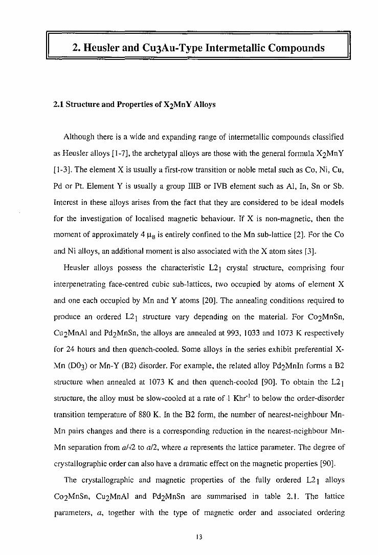
The results of an SAPW calculation for Cu2MnA1 are shown in figures 2.1 (a) and (c)
[ 16]. From the figures, it can be seen that the majority- and minority-spin bands for Cu
3d-derived states are almost completely occupied, as are the majority-spin Mn 3d
derived states. In contrast, however, the minority-spin Mn 3d-derived states are located
14
~ c
13.0 " ..... ·~ .:·.!!·· z;o
':-~
~ 1.0 Q
Figure 2.1
-- maj.spin ---· min. spin
4 3 2 I 0 ·I 4
Binding Energy (eV)
0.5 c
.Si 11 0.0 ·;:;
" ~ -0.5
·1.0 ...... ~~-~~~-~"""' 5 4 3 2 I 0 ·I ·2
Binding Energy (eV)
The results of a symmetrised augmented plane wave calculation for the ternary Heusler alloy
Cu2MnAl (adapted with permission) {16]. The figures show the spin-projected partial density of
states and corresponding polarisation for (a) and (b) the Cu 3d band and (c) and (d) the Mn 3d
band respectively. Binding energies are referenced to the Fermi level, which is arbitrarily set at
zero.
mainly above the Fermi level, EF, and are almost completely unoccupied. The
corresponding valence band polarisations for the Cu and Mn d bands are shown in
figures 2.1 (b) and (d). Polarisations, P,, (£8 ), were calculated according to the
relationship
(2·1),
15

where D,(E8 )r and D,(E8 )• represent the spin-up and spin-down partial density of
states (PDOS) for the element, 11, at a binding energy, E8 • Theoretical calculations on
the series of X2MnY alloys indicate that the lattice constant is mainly determined by the
choice of element X. The role of the element Y is to provide p orbitals that mediate the
covalent Mn-Mn interaction [20]. The occupation of the resulting p-d hybrids has a
strong influence on the magnetic order, as demonstrated experimentally by Webster and
eo-workers for the systems Pd2MnlnxSn 1-x and Pd2MnlnxSbJ-x [93-95]. The
magnetic ordering was found to change from antiferromagnetic to ferromagnetic as x
was progressively decreased. This change in magnetic ordering was associated with a
corresponding increase in the conduction electron concentration.
2.2 Structure and Properties of Pd2TiY Alloys
Recently, a new family of Heusler alloys based on Ti rather than Mn have been
discovered [5-7]. All alloys in the series can be produced in single phase highly ordered
L2J structures following annealing at 1073 K for 24 hours and quench-cooling. These
materials are of particular interest since they are reported to exhibit unusual magnetic
properties. A summary of crystallographic and magnetic properties is given in table 2.2.
Alloy a (nm) Order m (l!n) T(K)
Pd2TiAI 0.632 F 0.21 >900
Pd2Tiln 0.637 AF 4.9* 110*
Pd2TiSn 0.638 F 0.005 >300
Table 2.2
The crystal/agraphic and magnetic properties of Pd2TiY alloys [5·7]. The lattice parameter is
denoted by a. F and AF denote ferromagnetic and antiferromagnetic ordering respectively. For
Pd2TiAl and Pd2TiSn, the overall magnetic moments per formula unit are given by Ill and T
represents the Curie temperature. *For Pd2Tiln, m represeJl!s the effective paramagnetic moment
and T represents the associated Nee/ temperature.
16

• i6
(a) Pd2TIAI
" • ""' "' 8 2
11 tu • ,, 11
_, Binding Energy (cV)
• >
(b)l'd2Tiln
1 6
4 -" "' 8 2
• 6 • 2 • _, Ginding Energy (eV)
• ;:,, 6
~
" • s "' 8 '
Binding Energy (eV)
Figure 2.2
The total density of states for the ternary alloys (a) Pd2TiAl, (b) Pd2Tiln and (c) Pd2TiSu
calculated using the linear muffin tin orbital method. The figure is adapted from the original data
with permission [22, 23].
Magnetic ordering in intermetallic compounds that contain non-magnetic elements
has also been reported for Sc3In [96], Au4 V [97] and ZrZnz [98]. These alloys do not
exhibit localised magnetism, but instead have been classified as weak itinerant
ferromagnets. They are characterised by small moments and very low ordering
temperatures. Although the small moments obtained for PdzTiAl and PdzTiSn might
indicate weak itinerant magnetism, this classification is not appropriate since the Curie
temperature is excessively high in each case. The nearest-neighbour separation of the Ti
atoms in the PdzTiY series is almost the same as the Mn-Mn separation in the XzMn Y
17

series and is substantially larger than the radial extent of the 3d wavefunctions. It might
be expected, therefore, that the Ti-based alloys might also behave as localised magnets.
However, if the moment is localised on the Ti atoms and governed by Hund's tU le, then
the effective paramagnetic moment of 4.9 Jls reported for Pd2Tiin is difficult to
reconcile with the electronic configuration of Ti [6].
To further complicate the picture, linear muffin tin orbital (LMTO) calculations for
these materials indicate that all the Pd2TiY alloys should be paramagnetic [21-24]. It
has been suggested, therefore, that the reported magnetism may result from the presence
of magnetic impurities [21]. The results of the energy-band calculations for the alloys
Pd2TiY (Y = AI, In & Sn) are shown in figure 2.2 [22, 23]. The total density of states
(DOS) can be considered in three parts. The unoccupied Ti 3d states lie above EF.
Between EF and a binding energy of approximately 6 e V, the DOS is dominated by the
Pd d band. The occupied Ti 3d states also contribute throughout this region and both Pd
and Ti d states contribute at Ef' The s states of the element Y are located at the bottom
of the band and are separated from the main part of the occupied DOS. Substitution of
the element Y does not greatly affect the shape of the total DOS, but there is a
quantitative difference in the width and position of the gap between the s states of Y and
the d states of Pd.
2.3 Structure and Properties of Pt3Z Alloys
Pt forms a range of ordered intermetallic compounds of composition Pt3Z, where Z is
a first-row transition metal [I 0-15]. These materials exhibit a range of magnetic
properties. The alloys possess the face-centred cubic Ll2 (Cu3Au-type) structure [27].
This comprises four interpenetrating simple cubic sub-lattices, three occupied by Pt
atoms and one by atoms of element Z. Each Z atom has 12 nearest-neighbour Pt atoms
and 6 next-nearest-neighbour Z atoms. The Z atoms only have Pt neighbours, so there is
no direct Z-Z interaction. As is the case for the X2MnY Heusler alloys, the Pt3Z alloys
are considered to be ideal models for the investigation of localised magnetic behaviour.
18

Alloy Order mp, (!Jn) IUz (!Jn)
Pt3Ti p --- ---
Pt3V FI -0.30 1.00
Pt3Cr FI -0.26 3.37
Pt3Mn F 0.26 3.64
Pt3Fe AF --- 3.30
Pt3Co F 0.26 1.64
Table 2.3
Magnetic ordering and magnetic moments, mw associated with the element, n, for Pt3Z alloys in
the series Z = Ti, V, Cr, Mn, Fe and Co [10·15]. P, F1, F and AF represent paramagnetic,
ferrimagnetic,ferromagnetic and antiferromagnetic ordering respectively.
The annealing conditions required to produce a highly ordered LI2 structure vary
depending upon the element Z. For Pt3 V, the ingot is annealed at 1423 K for 72 hours
and then quench-cooled [ 11]. If annealed at 1203 K for 24 hours and then quench
cooled, the Pt3 V alloy adopts a tetragonal (TiAl3-type) st1ucture [99]. For Pt3Mn, the
ingots require a lower annealing temperature of 1223 K and are slow-cooled at a rate of
I Kmin·' [100]. The LI2 alloys Pt3V and Pt3Mn both possess a lattice parameter of
0.39 nm [99, 100]. The magnetic properties are strongly dependent upon the degree of
crystallographic order, with the atomically disordered alloys exhibiting paramagnetism.
The magnetic moments associated with the Pt and Z atom sites for a range of ordered
Pt3Z alloys are listed in table 2.3. Magnetic ordering temperatures are reported to be 206
K for Pt3V [11], and 395 K for Pt3Mn [lOO].
Band-structure calculations indicate that the exchange splitting for the Pt 5d states is
relatively small, but the corresponding splitting of spin-up (majority) and spin-down
(minority) states is comparatively large for the transition metal 3d states [25, 27, 30].
This explains the large local moments on the Z atom sites and the relatively small
moments associated with the Pt sites. The results of a tight-binding (TB) calculation of
the site- and spin-projected DOS for Pt3Mn are shown in figure 2.3(a) [27]. For the case
19

spin-down
s 4 3 ' l "''" ",;: .. ::-.·:,·"-;,. •:",
Binding Energy· (eV)
1.0
0.5
.!1 -~ 0.0 • • ~ totnl
,-1).5
·1.0
' 3 L., o lllndlng.Energy (eV)
Figure 2.3
Results of (a) tight-binding calculations of the total and Mn 3d partial density of states for the
binary alloy Pt3Mn (reproduced with permission) [27] and (b) the corresponding polarisations.
of Pt3Mn, the spin-up Mn 3d states are almost completely occupied and the spin-down
states are almost completely unoccupied. This explains the fact that the Mn sites in
Pt3Mn possess the largest local moment in the series (table 2.3). Figure 2.3(b) shows the
resulting valence band polarisations calculated using equation (2-1 ). The total valence
band polarisation has been determined by replacing the PDOS defined in equation (2-1)
with the total DOS. Due to the large difference in occupancy of the spin-up and spin
down 3d states in Pt3Mn, there is a correspondingly large positive 3d polarisation across
the valence band.
20

2.4 Summary
The binary Pt3Z alloys, together with the ternary Heusler alloys, are ideal models for
investigation of the electronic and magnetic properties of intermetallic compounds. As a
consequence, the band-structures have been calculated by a variety of methods and a
debate has been stimulated as to the nature of the local moment formation. However, in
many cases direct experimental investigation of the electronic structure has not been
performed. There is, therefore, a need to validate the theory by a systematic
photoemission study of the valence bands of these important materials.
21

3. Principles of the Experimental Techniques
3.1 Auger Electron Spectroscopy (AES)
Auger electron spectroscopy (AES) is a standard analysis technique for the
determination of surface elemental composition [101]. The sample under investigation
is bombarded with primary electrons in the energy range 2-5 keV. This results in the
creation of an initial hole by ionisation of a core level within an atom. The core hole is
then filled by de-excitation of an electron from an energetically higher-lying shell. This
transition may be accompanied by either X-ray fluorescence or by a non-radiative Auger
transition. In the latter process, the energy of the de-excited electron is transferred to a
so-called Auger electron, that is subsequently emitted with a characteristic kinetic
energy. Since the emitted Auger electron has a kinetic energy directly related to the
differences in core level energies, energy analysis of the emitted electrons can be used to
identify the element from which the electron originated. The surface sensitivity of AES
is derived from the limited escape depth of the Auger electrons, with a typical range of
0.1-0.3 nm. The sensitivity of the technique is approximately I % of a monolayer.
The nomenclature of Auger transitions reflects the electronic energy levels involved.
The three main branches are the KLL, LMM and MNN transitions. The first letter
denotes the shell in which the initial core hole is created, the second letter denotes the
shell from which an electron is de-excited to fill the core hole and the final letter denotes
the shell from which the Auger electron is ejected. For atoms bound in a solid,
transitions may involve electronic bands in addition to well-defined core levels and such
transitions are denoted with a V, for example LVV and MW. Strongest intensities are
then observed for processes in which the two final holes are produced in regions with a
high valence band density of states.
The characteristic kinetic energies of the emitted Auger electrons can be described in
terms of the difference between the corresponding core level energies, as measured by
22

X-ray photoelectron spectroscopy. In addition, a correction term is incorporated to
account for many-electron affects corresponding to the rearrangement of electrons
following the creation of an additional core hole. For example, the kinetic energy,
E(Z)KL,L,, of the Auger electron emitted by a KL1L2 process from an atom with atomic
number Z can be described by
E(Z)KL,L, = E(Z)K -E(Z)L, -E(Z\ -M:(Z)L,.L, (3·1).
The first three symbols on the right hand side of equation (3-1) define the K, L1 and L2
core level energies respectively and !1E(Zl~-,.~-, is the correction term. The correction
takes into account the increase in binding energy of the L2 electron when the L 1 electron
is removed and vice-versa. The correction term can be evaluated by empirically relating
the higher ionisation states of atom Z to the core level energies of the atom Z+ I as
follows,
The auger process involves several steps, but the crucial interaction is between the
electron de-excited to occupy the initial core hole and the emitted Auger electron. The
transition probability, WKL,L, , for a KL1L2 process, for example, can be described by
The transition probability can be calculated using a Coulombic interaction potential
for two electrons at r1 and r2 • Other symbols have their usual definitions. The one-hole
initial state is described by the 2s and 2p single-electron wave functions. The two-hole
final state contains electron #I in the Is state and electron #2 is described in terms of a
plane wave state with wave vector k . Many-electron effects are neglected in this
description. Unlike radiative transitions, the Auger transition probability ts
23

approximately independent of Z. In addition, Auger processes do not obey the dipole
selection rules, since the transition probability is governed by the Coulomb interaction
and not by a dipole matrix element.
Experimentally, AES requires an electron gun capable of producing primary
electrons in the energy range 2-5 keY. Energy analysis of the emitted Auger electrons
can be performed with a concentric hemispherical analyser (CHA), a cylindrical mirror
analyser (CMA) or a retarding field analyser (RFA). In the case of the CMA, the
electron gun is usually integrated into the analyser along its central axis. Because the
Auger peaks are comparatively weak compared to the inelastic background, the analysis
is usually performed in derivative mode. For analysis with a CMA, for example, a small
alternating voltage, vasinwt, is superimposed on the outer cylinder voltage, V. The AC
component of the signal from the electron multiplier passes through a capacitor to
decouple it from the DC component and the magnitude at the modulation frequency, w,
is detected by means of a lock-in amplifier. The pre-factor of this signal contains the
first derivative, d!/dV. Auger spectra are, therefore, usually defined in terms of the
derivative dN(E)IdE and the Auger line energies taken as the position of the minimum
of this derivative. For modulation voltages below the analyser resolution, the amplitude
is proportional to the modulation voltage but the peak shape is almost constant.
However, as the modulation voltage is increased beyond the analyser resolution, further
increases in amplitude are accompanied by a progressive loss of resolution. As a
consequence, the modulation voltage is chosen to provide a suitable compromise
between sensitivity and resolution.
3.2 Ultraviolet Photoemission Spectroscopy (UPS)
Ultraviolet photoemission spectroscopy is a widely used technique for investigation
of the electronic structure of metals and their alloys [59, 62, I 02]. The technique is
based on the photoelectric effect (section 1.3). A solid surface is irradiated under
vacuum by mono-energetic photons and the emitted electrons are energy analysed. The
24

most commonly used photon sources are either fixed energy He discharge lamps (He I =
21.2 eV, He II = 40.8 eV) or continuous energy synchrotron sources. Energy analysis of
the emitted photoelectrons can be performed using either a CHA or CMA. However, in
order to determine the dispersion of the electronic bands, the direction of emission as
well as the kinetic energy of the photoelectrons must be determined. This can be
achieved by employing an analyser with a small angular aperture, such as a VG ADES
400.
The total emission current, I(EK,hv), can be considered to be the sum of two
components, so that
where lp(EK,hv) and / 5 (EK,hv) represent the current of pnmary (elastic) and
secondary (inelastic) electrons. The photoemission process can be described in terms of
the so-called 3-step model [I 03]:
(1) Optical excitation of an electron from an initial to a final state within the solid.
(2) Propagation of the excited electron to the surface.
(3) Escape of the electron through the sample surface into the vacuum.
According to this model, the primary component can be factorised into a distribution of
photoexcited electrons, p(EK,hv), a transmission function, 't(EK,hv) and an escape
function, T](EK), so that
The internal electron current density directed towards the surface with an energy E K and
a wave vector k ( k-'- > 0) is given by
p(EK, hv) oc Il('1'1 (klJF1 'l';(kl)l' fm(E, )i\(E1(k)- E,(k)- hv)o(EK - E1(k)) (3-6). J .i
25

The matrix element represents the "golden-rule" transition probability between initial
and final states, denoted by '¥1(k) and '¥1(k) respectively. P is an appropriate
photoionisation operator [I 04). The transition probability depends on the joint initial
and final DOS, but for incident photon energies> 25 eV, the density of final states can
be assumed to approach the free-electron form [105]. The function fr0 (E,) is a Fermi-
Dirac distribution, ensuring that the initial states are occupied. The first o-function
ensures energy conservation in the excitation of an electron from E, (k) to E 1 (k). The
second o-function ensures that, for detection at energy EK, the energy of the final state,
E1 (k), is equal to EK.
The transmission function, 't(EK,hv), depends on the isotropic mean free path of the
electrons, 'A,(EK) and the attenuation length, 'A",(hv), of the photons. 't(EK,hv) is a
slowly varying function of energy with a value of- 0.1 for a typical metal at a photon
energy of 15 e V and can be described by the expression
A(EK,hV) T:(EK,hv) =
I+ A(EK,hv) where (3-7).
The elastic mean free path can be defined as the average distance electrons travel in the
solid between scattering events. Energy loss can occur by excitation of phonons, the
creation of electron-hole pairs or by the excitation of plasmons. Phonon scattering
changes the direction of the outgoing electrons, but only reduces the energy by the order
of meV. At low electron energies, the dominant loss mechanism is electron-hole
creation. However, at energies above the plasmon energy, plasmon excitations become
more significant. The surface sensitivity of UPS is, therefore, determined by the limited
escape depth of the primary electrons and is usually considered to be approximately 2
nm.
Escape from the solid is only possible for electrons with sufficient kinetic energy to
surmount the potential barrier Er+ <p , where <p is the work function and Er is the
Fermi level. For an isotropic distribution of electrons inside the solid, the fraction that
escape, T](EK), is given by
26

(3-8a),
(3-Sb).
Both -c(EK,hv) and l'\(EK) are smooth functions of EK beyond the low energy cut-off
and so do not give rise to structure in lp(EK,hv).
Transmission of the electron through the surface into the vacuum requires that the
wave vector component parallel to the surface, k 11 , is conserved. However, the wave
vector component normal to the surface, k ~, is not conserved. For the external electron
on the vacuum side of the surface, the wave vector, k" , is determined by energy
conservation,
= li'(k~'' + k;;')
(3-9). 2m
The wave vector components parallel and perpendicular to the surface outside the solid
can be determined from known experimental parameters,
I
k'' = (ZmEK )'sinS " n2 and (3-10),
where e defines the angle between the surface normal and the emission direction of the
photoelectron, the so-called take-off angle. In order to determine the dispersion of 3-
dimensional bulk band-structures, the k ~ component inside the solid must be
determined. this is usually achieved by obtaining photoemission spectra at normal take
off, so that e , k 11 and k;; are all equal to zero. The wave vector components k ~and
k:' are related through energy conservation and by assuming free-electron-type final
states, such that
(3-11).
27
V0 , the inner potential, can be assumed to be the zero of a muffin-tin potential. If
theoretical calculations are available for the final states, then these may be used instead
of the assumed free-electron parabolae.
There are 3 main experimental modes for obtaining photoemission spectra and these
can be summarised as follows:
(I) Electron energy distribution curves (EDCs) are obtained by varying the detected
photoelectron kinetic energy, but maintaining a fixed photon energy.
(2) Constant-initial-state (CIS) spectra are obtained by synchronous variation of the
detected photoelectron kinetic energy and incident photon energy such that the
difference between them remains constant. This permits emission from the same initial
state to varying final states and can be used to highlight resonance effects and Cooper
mmtma.
(3) Constant-final-state (CFS) spectra are obtained by detecting photoelectrons at a fixed
kinetic energy, whilst varying the incident photon energy.
3.3 Photoionisation Cross-Sections and the Cooper Minimum
The photoionisation cross-section, cr"1(EK), can be defined as the transition probability
per unit time for the excitation of a single photoelectron from the nl sub-shell of interest
under an incident photon flux of lcm·2s· 1• According to the discussion of Cooper [33),
the photoionisation cross-section of a many-electron atom is given by
(3-12).
'f', and '¥1 are the atomic wavefunctions before and after photon absorption described
in terms of the electron co-ordinates r1 • The symbols a 0 and a0 define the fine-
structure constant and the Bohr radius respectively. The (positive) kinetic energy of the
emergent photoelectron and the (negative) binding energy of the electron in the nl sub-
28

shell are denoted by EK and E8 respectively. The units of energy are Rydbergs and the
cross-section is defined in units of cm2• The sum is over all atomic electrons and the
integration is over all electron configuration space. If it is assumed that '¥; and '¥1 are
composed of None-electron wave-functions and that N-1 remain in the same initial and
final states, then equation (3-12) reduces to
(3- 13).
Atomic sub-shell photoionisation cross-sections, cr.,JEK), have been calculated by Yeh
and Lindau, employing the Hartree-Fock-Slater one-electron central potential model
[106]. The cross-sections, after summing over possible final states and averaging over
initial states of quantum number m can be defined as
cr (£) = (4n'a,a;J(N,,(EK-E,))((l+I)R' (E)+ IR' (El] nl K 3 2/ + l I+ I K 1-1 K
(3-14).
N.,, is the number of electrons in the n/ sub-shell. The one-electron radial dipole matrix
elements, R1±1 (EK), can be expressed in the "length" approximation as
R1"(EK) = J P,,1(r)rPE.I±I(r)dr (3-15),
"
where P,,(r) I r and PE.l±l(r) I r are the initial (discrete) and final (continuum) state
one-electron radial wavefunctions respectively. The radial component of the initial state
is described in terms of the one-electron SchrOdinger equation,
(d' /(I+I)J dr' + V(r)+E,--,-2 - P,,(r) = 0 (3-16),
where V(r) is the sum of the Coulombic and free-electron exchange potentials [107].
The final state is approximated by the same potential field, but the electron is removed
29

to a continuum state of energy E. The radial component of the final state is, therefore,
described by the analogous Schrodinger equation,
(.:£.._ V() E l±l(l±l+l))P. () O 2 + r + K , £1±1 r = dr r· ·
(3-17).
From equation (3-14), it can be seen that the cross-sections are dictated by the character
of the radial wavefunctions and are therefore influenced by the n and l values. For a
given value of I for the initial state, the final states comprise two angular momentum
states of values I+ I and 1-1, referred to as the "up" and "down" channels respectively.
There are n-1-1 nodes in a radial wavefunction characterised by the quantum numbers
nl. For wavefunctions that do not contain radial nodes, for example 2p and 3d states, the
photoionisation cross-section increases to a maximum at or just above threshold and
then decreases monotonically as the photon energy and therefore the photoelectron
kinetic energy is increased. However, initial states with wavefunctions possessing a
radial node exhibit a cross-section that displays a characteristic minimum. This effect,
originally predicted by Cooper [33], arises from the cancellation of the "up" channel
matrix element integral for transitions to particular final states and is particularly
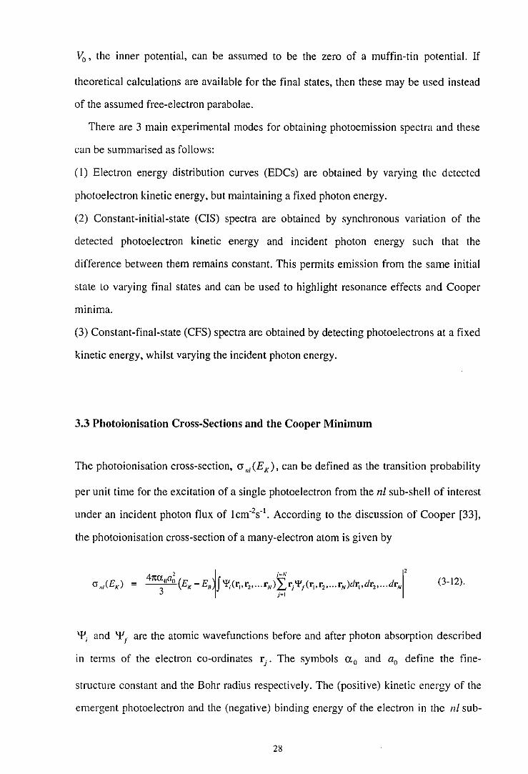
pronounced when only a single node is present (n = 1+2). Figures 3.1(a) and (b) show
the modified radial components of the initial state wavefunctions for Ne 2p and Ar 3p
respectively [33]. The spectral behaviour of the photoionisation cross-section will be
dominated by the matrix element integral for the "up" channel. Consequently, the
corresponding modified radial components of the associated I+ I continuum
wavefunctions at photoionisation threshold ( EK = 0) are also shown. From figure 3.1 (a)
for Ne, it can be seen that the d-wave matrix element integral is small and positive at
threshold. As the photoelectron kinetic energy increases, the spatial periodicity of the
final state wavefunction will be reduced and the position of the first node will move
closer to the nucleus. This will initially result in an increase in the matrix element
integral, subsequently followed by a monotonic decline as the the first node of the
continuum wave becomes sufficiently close to the nucleus that negative contributions to
the integrand become important. For the case of Ar shown in figure 3.1 (b), the d-wave
30

1.0
0.5
2p initial state (a) Ne
0.0 ,
-0.5
·I::' ~ -1.0 c..?,, 1.0
0.5
0.0
-0.5 3p initial state
-1.0
0.0 0.2 0.4 0.6 0.8
r (nm)
Figure 3.1
Modified sub-shell radial wavefunctions, P,/r) and PE/r), for initial (discrete) and final
(continuum) states of (a) Ne and (b) Ar at photoionisation threshold [33]. The radial distance
from the centre of the nucleus is defined by the symbol r.
matrix element integral is large and negative at threshold; but decreases in magnitude as
the photoelectron kinetic energy increases and the spatial periodicity of the continuum
wave is reduced. The matrix element integral for the "up" channel of the Ar 3p initial
state vanishes when negative and positive contributions to the integrand are identical. At
higher energies, the matrix element integral becomes positive. The energy dependence
of the I+ I matrix element integrals is illustrated in figure 3.2(a) for transitions from Ne
2p and Ar 3p initial states [33]. It can be seen from the figure that the "up" channel
matrix element integral vanishes for transitions from the Ar 3p initial state at
approximately 27 eV above threshold. The photoionisation cross-section for Ar 3p
calculated by Kennedy and Manson is shown in figure 3.2(b) [108]. The theoretical
calculation assumes the dipole "length" approximation and includes transitions to both d
and s final states. In this case, the cancellation of the d-wave matrix element integral
manifests itself as a pronounced Cooper minimum in the cross-section at approximately
31
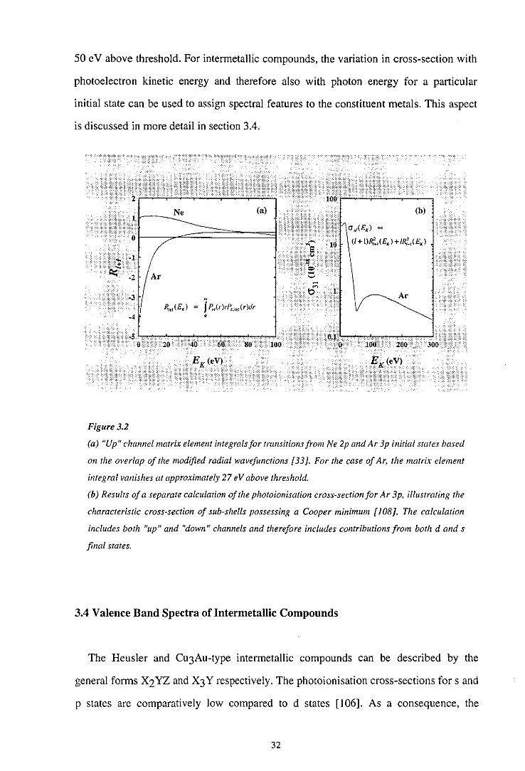
50 e V above threshold. For intennetallic compounds, the variation in cross-section with
photoelectron kinetic energy and therefore also with photon energy for a particular
initial state can be used to assign spectral features to the constituent metals. This aspect
is discussed in more detail in section 3.4.
(b)
a •1(EK) oc
(I+ l)R1!_1(Ex) +1RL1(EK)
Ar
-4
20 '40 .·66'. 80. lOO 0"1 o· . lOiF 200
Ex<eV) Ex (eV)
Figure3.2
(a) "Up" channel matrix element integrals for transitions from Ne 2p and Ar 3p initial states based
on the overlap of the modified radial wavefunctions [33 ]. For the case of Ar, the matrix element
integral vanishes at approximately 27 eV above threshold.
(b) Results of a separate calculation of the photoionisation cross-section for Ar 3p. illustrating the
characteristic cross-section of sub-shells possessing a Cooper minimum [JOB]. The calculation
includes both "up" and "down" channels and therefore includes contributions from both d and s
final states.
3.4 Valence Band Spectra of lntermetallic Compounds
The Heusler and Cu3Au-type intermetallic compounds can be described by the
general forms Xz YZ and X3 Y respectively. The photoionisation cross-sections fors and
p states are comparatively low compared to d states [106]. As a consequence, the
32
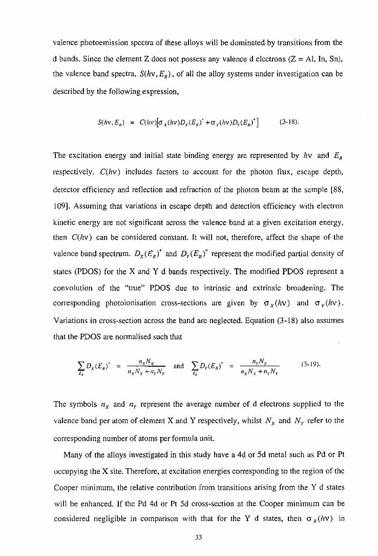
valence photoemission spectra of these alloys will be dominated by transitions from the
d bands. Since the element Z does not possess any valence d electrons (Z = AI, In, Sn),
the valence band spectra, S(hv,£8 ), of all the alloy systems under investigation can be
described by the following expression,
(3-18).
The excitation energy and initial state binding energy are represented by hv and E8
respectively. C(hv) includes factors to account for the photon flux, escape depth,
detector efficiency and reflection and refraction of the photon beam at the sample [88,
I 09]. Assuming that variations in escape depth and detection efficiency with electron
kinetic energy are not significant across the valence band at a given excitation energy,
then C(hv) can be considered constant. It will not, therefore, affect the shape of the
valence band spectrum. Dx<Eef and Dr(E8 )' represent the modified partial density of
states (PDOS) for the X and Y d bands respectively. The modified PDOS represent a
convolution of the "true" PDOS due to intrinsic and extrinsic broadening. The
corresponding photoionisation cross-sections are given by cr x(hv) and cr r(hv).
Variations in cross-section across the band are neglected. Equation (3-18) also assumes
that the PDOS are normalised such that
and (3-19).
The symbols nx and nr represent the average number of d electrons supplied to the
valence band per atom of element X and Y respectively, whilst N x and N r refer to the
corresponding number of atoms per formula unit.
Many of the alloys investigated in this study have a 4d or Sd metal such as Pd or Pt
occupying the X site. Therefore, at excitation energies corresponding to the region of the
Cooper minimum, the relative contribution from transitions arising from the Y d states
will be enhanced. If the Pd 4d or Pt Sd cross-section at the Cooper minimum can be
considered negligible in comparison with that for the Y d states, then cr x (hv) in
33

equation (3-18) can be taken as zero and the spectrum will reflect the shape of the
PDOS for the d band of element Y. Equation (3-18) is, therefore, assumed to reduce to
the expression
(3·20),
where hv c represents the photon energy corresponding to the Cooper minimum in the
cross-section of the X d states. The X PDOS can then be determined by employing
spectra obtained at an excitation energy well away from the Cooper minimum. The
PDOS are constrained according to equation (3-19) and the normalisation constant,
C(hv), is obtained by means of an iterative procedure. Differences in cross-section
between the photon energies employed can be accounted for using the calculated values
of Yeh and Lindau [106]. The method is identical to that used by Wright et al. to
determine the PDOS for Cu3Pd [8].
3.5 Resonant Photoemission
Resonant photoemission occurs when two separate paths connect the same initial and
final states. For example, at photon energies across the region of the 3p threshold,
photoemission from a 3d state can occur either directly, or via promotion of a p electron
to an unoccupied d state followed by autoionisation. The interference of the direct and
indirect processes results in a characteristic modulation in photoemission intensity and
the resulting lineshape is described theoretically by Fano [35]. The process can be
described as follows,
3p'3d"~3p6 3d"-' +e- (3-21a),
3p6 3d" ~3p'3d"•'----'>3p'3d"-' + e- (3-21b).
34

The modulated photocurrent, I mod (hv, E 8 ), can be expressed as
= l(hv E )[{q(E,) + e(hv,E,)}'] + I (hv E) I •n 1+e(hv,En)2 nr •a
where = 2{hv - hv0 (E,)} 1(£,)
(3-22b).
(3-22a),
l,.(hv, E8 ) and l,,(hv ,E8 ) represent the photoemission intensities resulting from direct
emission of electrons that do and do not contribute to the resonance respectively. The
Fano parameters that characterise the modulation are the resonance energy, hv 0 , the
asymmetry parameter, q, and the spectral width of the autoionised state, r. The Fano
parameters for a 3p-to-3d resonance can be described by the following set of equations,
hv" = hv. + PfiM,CKi' dv v.-v
(3-23a),
q = (3dl~3p) (3-23b),
(3-23c),
e' = (E/,3pj-l3d,3d)
r (3-23d).
Matrix element integrals are denoted in the Dirac bracket notation. The excitation
energy for the promotion of a 3p electron to a 3d valence state is given by hv. and
M,cK represents the matrix element integral for the subsequent super Coster-Kronig
decay of the resulting 3p core hole (autoionisation). P represents the "principal part" of
the integral in equation (3-23a). The symbols l3p), I 3d) and !El) represent
wa vefunctions for the 3p, 3d and continuum electron states respectively. Although
q(E8 ) and r(E8 ) are in fact functions of both the binding and excitation energies, the
excitation energy dependence of the parameters is neglected and they are considered
35

constant characteristics of a resonant profile at a given binding energy. Typical Fano
lineshapes are shown in figure 3.3. It can be seen from the figure that variation of the
asymmetry parameter has a profound effect on the lineshape.
10
q=J
8
..,...., 6 "' + ........
""" N .·,
W' + 4 ~
2
0
-10 -5 0 5 10
£
Figure 3.3
Fa no lineshapes obtained for different values of the asymmetry parameter q( £8). Symbols are
defined in the text.
Resonant photoemission is not confined to 3p-to-3d transitions, but has also been
observed for 4p-to-4d, 5p-to-5d and 4d-to-4f transitions [37, 110]. Since the effect is
atom specific, it can be used to identify the atomic origins of spectral features in valence
band spectra and is particularly useful in the elucidation of the PDOS. Distortion of the
3d wavefunction by hybridisation results in modification of the matrix element integrals
governing the asymmetry parameter. Therefore, analysis of 3p-to-3d resonant lineshapes
and the extraction of the associated Fano parameters can potentially provide information
on the localisation of 3d states across the valence band [89, Ill, 112].
In addition to the one-electron resonances described above, two-electron resonances
have also been reported for the first-row transition metals [113, 114]. This is considered
36

to involve resonant enhancement of a shake-up satellite located at a slightly higher
binding energy than the main valence band. The process is analogous to that described
by equations (3-21 a) and (3-21 b), but involves an electron excited to a low-lying nl state
and two 3d holes in the final state. The corresponding equations for the direct and
indirect processes are given by
3p03d" 4s~3p03d"-' 4s(nl) + e- (3-24a),
3p6 3d" 4s ~ 3p' 3d" 4s(nl)----. 3p6 3d"-' 4s(nl) + e- (3-24b).
As the processes described by equations (3-24a) and (3-24b) involve the same initial and
final states, a Fano-type resonance can occur. For transition metals with partially filled d
bands the excited nl electron is mainly 3d [114]. However, for the case of Cu, the
excited electron must occupy a 4s state, as there are no unoccupied d states available
[I I 3]. The presence of resonantly-enhanced satellites in the photoemission spectra of Ni
is well documented. However, for the transition metals Cr-Co, it has been suggested that
the reported satellite features may, alternatively, be explained by 0 2p emission from
contaminated surfaces [I 15].
37
,, 4. Experimental Details
4.1 The Synchrotron Radiation Source (SRS)
All photoemission measurements were performed at the 2 Ge V second-generation
synchrotron radiation source (SRS) at Daresbury [ 116]. At the SRS, electrons are
maintained in a circular orbit by a magnetic field and emit Bremsstrahlung radiation.
The radiation is emitted tangentially to the orbit of the beam with - I mrad vertical
divergence and is linearly polarised in the horizontal plane. The source size at the centre
tangent of dipole magnet 6, from which radiation for this study was taken, is
approximately 2.0 mm FWHM (horizontal) and 0.4 mm FWHM (vertical). The spectral
range extends from the far infrared, through vacuum ultraviolet to the hard X-ray regime
(10.4 eV to 105 eV), with a maximum flux output of 1013 photons/s/mrad
(horizontai)/Amp/0.1% bandwidth. Flux output exhibits a sharp decline at wavelengths
less than a critical wavelength, Ac, the so-called X-ray cut-off. For a bending magnet of
1.2 T, Ac is 0.388 nm. However, by incorporating 5T and 6T superconducting Wiggler
magnets, Ac can be reduced to 0.093 and 0.078 nm respectively.
The procedure for producing a stored beam involves a number of sequenced
operations. Initially, a 12 MeV linear accelerator injects electrons into a booster
synchrotron, where they are accelerated to an energy of 600 Me V. The booster has a
radius of 5.06 m and the electrons are guided by 0.786 T magnets with a bending radius
of 2.55 m. A typical beam current of 20 mA is maintained in the booster, comprising
approximately 53 electron bunches. Electrons are then extracted from the synchrotron
and injected into a storage ring until a beam current of approximately 250 mA is
achieved. The storage ring has a radius of 15.28 m (96.0 m circumference) and
comprises 16 dipole bending magnets ( 1.2 T) separated by straight sections. Each
magnet has a bending radius of 5.56 m. Electrons are ramped in energy by increasing the
field strength of the magnets until a final energy of 2 GeV is attained. In multi-bunch
38
,,
mode, the storage ring contains a maximum of 160 electron bunches, with a bunch
length of 0.18 ns (FWHM) and a repetition rate of 500 MHz corresponding to a 2.0 ns
bunch spacing. Energy lost from the beam due to the emission of electromagnetic
radiation is replenished by radio-frequency cavities. Under normal vacuum conditions
(<I o·9 mbar), beam lifetimes of 20-30 hours can be achieved. However, electrons are
still scattered out of the beam orbit by collision with residual gas molecules. This results
in a gradual decline in the beam current over the period of operation. As a consequence,
the ring is refilled at least once every 24-hour cycle.
4.2 SRS Beamlines 6.1 and 6.2
Beamlines 6.1 and 6.2 at the SRS are ultrahigh vacuum stations dedicated to
photoemission studies [117, 118]. The experimental chambers can initially be evacuated
to a pressure of approximately 5 x 10⁻² mbar using a combination of carbon-vane pumps
and liquid-nitrogen-cooled sorption pumps. Thereafter, pumping can be maintained by
rotary-backed turbomolecular pumps and titanium sublimation pumps. Both stations are
capable of achieving base pressures of I x 10'10 mbar or less following a 453 K bakeout
for 36 hours.
Station 6.1 has an effective photon energy range of 40-200 eV and delivers a flux of
approximately 10 11 photons/s/1 00 mA beam current. Radiation from the SRS is
deflected in the horizontal plane by a cylindrical Pt-coated SiC premirror and is incident
via an entrance slit on the monochromator. This comprises one of two plane gratings.
Both gratings have a line density of 1200 lmm' 1, but one is lamellar and the other
blazed. The diffracted radiation is then focused vertically through the monochromator
exit slits by one of two Au-coated spectrosil spherical mirrors. The radiation is then
post-focussed by a Au-coated spectrosil ellipsoidal mirror.
Station 6.2 has an effective photon energy range of 15-140 eV and also delivers an
approximate flux of 10 11 photons/s/100 mA beam current. Radiation from the SRS is
initially deflected horizontally and then vertically by two cylindrical SiC premirrors. The
39

vertically deflecting mirror is coated with Pt, whilst the horizontally deflecting mirror,
although originally Pt-coated, has been re-coated with Ni. The deflected radiation passes
through an entrance slit onto the monochromator, comprising two toroidal gratings. The
first grating has a line density of710 lmm· 1 and an effective photon energy range of 15-
60 eV. The second grating has a line density of 1800 lmm· 1 and an effective photon
energy range of 40-140 eV. The diffracted beam passes through the monochromator exit
slits and is then vertically deflected and post-focussed by two Au-coated spectrosil
mirrors, the first plane and the second ellipsoidal.
For both stations, selection of the required photon energy is achieved by adjusting the
grating angle. The photon energy resolution depends upon the size of the photon beam
at the entrance slit, the monochromator aberration and the vertical size of the exit slit.
The total beamline resolution is determined by summation of the three contributions in
quadrature. As the photon energy is increased, the size of the exit slit needs to be
reduced to maintain constant resolution. Movemement of the grating (6.1 and 6.2) and
exit slits (6.2 only) is computer controlled via stepper motors and Heidenhain encoders.
The exit slits on station 6.1 are adjusted manually. Variations in photon flux due to the
transmission characteristics of the monochromator and changes in beam current are
monitored by a W grid with 92 % transmission. This beam monitor is positioned
between the post-focussing optics and the experimental chamber. Photoemitted
electrons are measured as drain currents and converted to voltages using Keithley
cmTent-voltage amplifiers. The signal is then pulse counted after passing through a
voltage-frequency converter.
Changes in the SRS vertical beam position, or movement of the premirrors due to the
heating effects of the incident radiation, will result in a corresponding change in the
angle of incidence of the beam on the monochromator. This alters the wavelength of the
radiation at the exit slit away from the required value. Consequently, beam alignment
must be checked every 2-3 hours. This is performed by winding phosphor coated
defining jaws in to the path of the beam and by finely adjusting the angle of the grating
to maximise the beam monitor signal for zero-order radiation.
40
Although a choice of energy analysers is available for both stations, all reported
measurements were obtained with a Physical Electronics PHI model 15-255g cylindrical
mirror analyser (CMA). This is a double-pass, angle-integrating analyser with
hemispherical retarding grids and two interchangeable apertures of 4 mm (XPS) and I
mm (AES). The analyser is also equipped with an integral electron gun for AES,
providing beam energies of 100-5000 eV. The resolution of the analyser depends on the
mode of operation. In retarding mode, the manufacturer's specification quotes a
resolution of 1.2 % of the pass energy for the AES aperture and 2 % of the pass energy
for the larger XPS aperture. In non-retarding mode, it is quoted as 0.6 % of the kinetic
energy for the AES aperture and 1.6 % of the kinetic energy for the XPS aperture. The
potential of the cylinders can be adjusted to detect electrons with kinetic energies in the
range 0-2000 eV. The potential of the retarding grids can be adjusted to give pass
energies in the range 5-200 eV, with count rates approximately prop01tional to the pass
energy. The electron detector is a Gallileo 48310 channel electron multiplier. The gain
depends upon the operating potential and increases sharply from almost zero to a
plateau. The multiplier potential is maintained at a value just high enough to reach this
plateau. This is usually about 2.0 kV for a new channeltron, but may progressively
increase to 2.5 kVover a sustained period of use.
4.3 AES and UPS Measurements on the Alloy Systems
The alloy samples, supplied by the Condensed Matter Group at Loughborough, were
prepared by argon arc melting stoichiometric proportions of the high purity constituent
metals. Samples were then annealed in evacuated quartz ampoules under the conditions
outlined in section 2 for producing ordered L21 and L12 structures. After manufacture,
samples were characterised by electron probe microanalysis and X-ray diffraction to
confirm the bulk composition and crystallographic structure. Portions of the ingots to be
used for photoemission measurements were cut to shape by spark erosion and the front
faces polished, initially with SiC, then with successive grades of diamond paste to give a
41

final finish of I J.lm. Samples were then mounted on a stainless steel platen and held in
place with spotwelded tabs. Before being attached to the sample manipulator, all
components were cleaned ultrasonically in a degreasing solvent bath.
All measurements were performed on either beamline 6.1 or 6.2 at the Daresbury
SRS, depending upon the range of photon energies required. Base pressures of I x I o-IO
m bar (6.1) and 5 x 10' 11 mbar (6.2) were maintained throughout the period of data
acquisition. Sample surfaces were cleaned in situ by mechanical abrasion using a
diamond file mounted on a wobble stick. As-loaded samples were initially scraped for
approximately I 0 minutes, taking care to ensure that the polished layer was completely
removed. Subsequently, samples were scraped for about 2 minutes every 3-4 hours to
remove any contamination arising from the adsorption of residual gases. The elemental
composition of the surface was investigated before and after scraping by Auger electron
spectroscopy. This allowed levels of surface contamination to be monitored. In addition,
by quantification using appropriate sensitivity factors, the stoichiometry of the scraped
surface could be investigated. Cleaning of the sample surfaces by ion bombardment was
not used, since preliminary investigations on the Pd-based alloys indicated that
sputtering with 500 eV Ar+ at ion currents of 5 J.lA resulted in a non-stoichiometric Pd
rich surface. Energy analysis of the emitted electrons was performed by a Physical
Electronics angle-integrated double-pass CMA aligned at 90° to the direction of
incidence of the photon beam in the horizontal plane. Samples were earthed for all the
AES and UPS measurements.
AES was performed in differential mode with the sample at normal incidence to the
electron energy analyser. A primary beam voltage of 3 ke V was employed, with an
emission current of 0.5 mA and a peak-to-peak modulation of 3 eV. The electron
multiplier voltage supply was set at 1.0 kV and the small (I mm) aperture was in place.
UPS measurements were obtained in two different modes. Electron energy distribution
curves (EDCs) were obtained by varying the detected electron kinetic energy (EK) at a
constant photon energy (hv). Constant-initial-state (CIS) measurements were obtained
by allowing the photon energy and detected electron kinetic energy to vary
synchronously such that hv-EK remained constant. This allowed the photon energy
42
dependent emission intensity of initial states to be investigated. EDCs were obtained in
the photon energy range 20-180 eV. CIS spectra were obtained primarily in the photon
energy range 25-55 e V, across the region of the 3p thresholds for Ti, V and Mn. For
photoemission, the CMA was operated in retarding mode with a pass energy of I 0 e V.
The large (4mm) aperture was utilised and the electron multiplier setting was
approximately 2.2 kV. Over a period of time, this was increased to 2.5 kV to
compensate for degradation in performance of the multiplier. Photoemission spectra
were initially obtained from different regions of each ingot and employing a range of
take-off angles. However, no discernible differences in spectral shape were observed,
and all reported spectra were obtained from the centre of the sample face at a take-off
angle of 45°.
4.4 Data Analysis
EDCs were normalised to the reference signal from the bearn monitor. This
accounted for variations in photon flux arising from the transmission characteristics of
the monochromator and reductions in beam current over a 24-hour cycle. Binding
energies were referenced to the Fermi level, Ep. which was arbitrarily assigned a value
of zero. As there are only unoccupied states above Ep. no photocurrent should be
observed in this region. However, a small background results from electrons emitted by
higher-order radiation. This background intensity, I 8 , was assumed to be uniform across
the entire valence band region and subtracted from the flux normalised photoemission
intensity, I' (E8 ). The resulting corrected intensity, I(E8 ) is, therefore, defined as
The inelastic secondary electron background was removed from each spectrum using a
Shirley algorithm with 3 iterations [119]. This procedure assumes that the secondary
electron contribution at each binding energy is proportional to the total sum of
43
intensities to lower binding energy. The photoemission intensity obtained after removal
of the inelastic contribution, l 0 (E8 ), is related to the intensity before removal, l(E8 ),
by the expression
111(E8 ) = I(E8 ) - I(E11 )j(E~) (4.2).
The emission intensity l(E0 ) corresponds to that obtained at a binding energy where the
entire contribution is from secondary electrons. The function f(E~) is given by
A typical valence band photoemission spectrum for the CuzMnAI Heusler alloy is
illustrated in figure 4.1(a). The spectrum was obtained at a photon energy of 40 eV and
has been flux-normalised. The solid curve corresponds to the photoemission intensity,
I'(En). The various broken curves in figure 4.1(a) indicate the inelastic background
calculated using a Shirley algorithm with successive iterations. The inelastic background
calculated after 3 iterations has been subtracted from the solid curve in figure 4.1 (a) to
produce the curve in figure 4.1 (b). The latter, therefore, corresponds to the background
subtracted photoemission intensity l 0 (E8 ).
The effect of instrumental resolution on spectral shape was estimated by fitting
Fermi-Dirac distributions, JFD, of the form
convoluted with Gaussians of varying HWHM to the Fermi edge region of the EDCs. In
the photon energy range 40-90 eV, under the experimental conditions defined in section
4.3, reasonable fits were obtained for Gaussians of HWHM between 0.2-0.3 e V.
For CIS spectra, the analysis procedure also involved normalisation to the beam
monitor signal. In some cases, the inelastic contribution was retained and no further data
44

8 6
Figure 4.1
(a)
- S[lt.'Cirnm
··· iteration 1 --· iterution :Z -··- itcrution 3
(b)
Binding Energy (eV)
·2
(a) Flux-normalised photoemissiou spectrum of the ternary alloy CuzMnAl obtained at a photon
energy of 40 eV, together with successive iterations of the inelastic background using a Shirley
lligorithm.
(b) The corresponding flux-normalised spectrum obtained by subtracting the inelastic background
calculated after 3 iterations from the solid curve in figure 4./(a).
manipulation was attempted. However, in order to quantitatively fit lineshapes to
resonant features, it was necessary to remove the inelastic contribution. This is
necessary because the photoemission current from initial states at higher binding
energies will comprise an increasing inelastic contribution, as demonstrated in figure
4.1 (a). This inelastic contribution will also exhibit a modulation across the photon
energy range of the resonance, as a result of energy losses from electrons originating
from states closer to EF. Consequently, in order to obtain a true picture of resonant
modulation across the valence band, it is desirable to separate the elastic and inelastic
contributions. The procedure for removal of the inelastic background from a typical
45

Figure 4.2
(b)
46. 48 so sz s4
Photon Energy (eV)
(a) The curve labelled (I) shows a typical flux-normalised constant-initial-state spectrum for the
Heusler alloy PdzMnSn. The spectrum was obtained for an initial state binding energy of 2.5 eV,
across the photon energy range corresponding to the Mn 3p threshold [ 120]. The spectrum
comprises both elastic and inelastic contributions. The curve labelled (11) shows the resulting
spectrum obtained by subtracting the calculated inelastic contribution, shown as the solid curve in
part (b),from curve(/).
(b) Data points (solid circles) represent the inelastic background calculated from the
corresponding electron energy distribution curves using a Shirley algorithm. The solid curve
represents the resulting smooth background obtained by fitting a fourth-order polyno111ial to the
data points. Further details are supplied in the text.
Pd2MnSn CIS spectrum (E8 = 2.5 eV) is illustrated in figures 4.2(a) and (b). Curve (I)
in figure 4.2(a) shows a flux-normalised CIS spectrum obtained in 0.1 eV increments
across the photon energy range corresponding to the Mn 3p threshold [ 120]. The
photoemission current comprises both elastic and inelastic contributions. Curve (11)
shows the corresponding reconstructed spectrum obtained by subtracting the calculated
46

inelastic contribution from curve (I). The calculation of the inelastic background was
accomplished by obtaining a series of EDCs at coarse photon energy increments across
the excitation energy range of the CIS spectrum. Each EDC was normalised so that the
photoemission intensity at a binding energy of 2.5 eV was consistent with the CIS
spectrum (I) and the inelastic contribution calculated using a Shirley procedure. The
resulting reconstructed background is shown as the data points in figure 4.2(b). A
smooth inelastic background was fitted to the data obtained from the EDCs using a
fourth-order polynomial, shown as the solid curve in figure 4.2(b), then subtracted from
the flux-normalised CIS spectrum (I) to give the reconstructed CIS spectrum (II). This
procedure was repeated for CIS spectra obtained at binding energies across the valence
band, to allow for a more accurate evaluation of the variation in resonant lineshapes.
Quantitative Fano analyses were only performed on reconstructed, background
subtracted CIS spectra.
47

5. Results and Discussion for X2Mn Y Alloys
5.1 Determination of Surface Composition by AES
0
c
Sn Sn Mn Mn Mn
Sn
Pd (c)
C Sn Sn Sn Mn Mn CoCo
Co Sn
(d)
c
Mn
Cu+Al 1000 2000
1000
Figure 5.1
Auger electron spectra of(a) as-loaded Pd2MnSn, (b) scraped Pd2MnSn. (c) scraped Co2MnSn
and (d) scraped Cu2MnAl in the kinetic energy range 0-1000 eV. Spectra have been displaced
along the ordinate for clarity. The inset shows the spectrum for CuzMnAl in the kinetic energy
range 1000-2000 eV. The scale of the ordinate for the inset has been arbitrarily expanded relative
to that of the main figure in order to show the relatively weak AI KLL transitions more clearly.
Spectra were obtained at normal incidence with 3 keV primary beam voltage and 3eV peak-to
peak modulation.
48

The surfaces of the alloy samples were cleaned in situ by mechanical abrasion with a
diamond file as described in section 4.3. In order to monitor the changes in surface
composition, Auger elecron spectra were acquired before and after scraping. The as
loaded samples were initially scraped vigorously for about 10 minutes. After initial
cleaning, scraping for about 2 minutes every 3-4 hours was necessary to remove
contamination arising from residual gases in the experimental chamber. The Auger
electron spectra for (a) as-loaded Pd2MnSn, (b) scraped Pd2MnSn, (c) scraped
Co2MnSn and (d) scraped Cu2MnAI are shown in figure 5.1. Spectra were obtained
with the samples at normal incidence to the analyser and employing a primary beam
voltage of 3 keV and a modulation of 3 eV peak-to-peak. The spectra have been
displaced along the ordinate and the scaling is arbitrary. The as-loaded sample clearly
shows heavy contamination of the surface by carbonaceous deposits with traces of 0, S
and Cl also present. The spectra of the scraped alloys, however, show Auger peaks
characteristic of the constituent metals. A residual C peak is observed in the spectrum of
the scraped Co and Cu alloys, but the presence of a small C peak in the Pd alloy may be
masked by the overlapping Pd Auger peak at 279 eV. All the alloys retained traces of S
and Cl on the surface even after vigorous scraping. It would seem likely, therefore, that
this contamination arises from the segregation of bulk impurities. Quantification was
performed by measurement of peak-to-peak heights for the LMM transitions of Mn, Co
and Cu at 589, 775 and 920 eV respectively, the MNN transitions of Pd and Sn at 326
and 430 eV respectively and the KLL transition of AI at 1396 eV. After correction using
literature values for the relative sensitivity factors [121], the surface stoichiometry was
found to be consistent with the nominal bulk composition within the limits of the
associated uncertainties.
5.2 Non-Resonant Photoemission
Representative EDCs for each scraped alloy are shown in figure 5.2. Photon energies
were selected to minimise the effect of differences in cross-section between the X and
49

Mn d states on the spectral shape. The spectra for Co2MnSn and Cu2MnAl were
obtained at a photon energy of 40 eV and the corresponding spectrum for Pd2MnSn was
obtained at 70 eV. As can be seen from figure 5.2(a), the valence band of Co2MnSn has
a bandwidth of 4-5 e V and is characterised by a high DOS immediately below Ep. This
contrasts with the valence band spectra of Cu2MnAl and Pd2MnSn, which reveal the
highest occupied DOS to lie approximately 3 eV below Ep in each case, with only a
relatively small shoulder extending as far as Ep. The bandwidths of the Cu and Pd alloys
are also significantly larger, extending approximately 6 and 7 eV below Ep respectively.
Comparing these results with earlier photoemission measurements on Heusler alloys, it
is apparent that the shape of the valence band spectrum of Co2MnSn is very similar to
that obtained for Ni2MnSb [89], whilst the valence band spectrum of Cu2MnAl is very
similar to that obtained in an earlierphotoemission study using a He I source [122].
Figure 5.2
Electron energy distribution curves for the valence band region of (a) CozMnSn (b) CuzMnAl
and (c) PdzMnSn. Spectra for the Co and Cu alloys were obtained at an excitation energy of40
e V in each case. The spectrum for the Pd alloy was obtained at an excitation energy of 70 e V.
Spectra have been flux-normalised and the inelastic contribution removed by means of a Shirley
algorithm.
50

5.3 Comparison with Band-Structure Calculations
An important application of UPS is to establish the validity of theoretical band
structure calculations. The band-structures of a range of X2Mn Y Heusler alloys have
been calculated using SAPW [16-18] and ASW [19, 20] methods, but the results have
not been verified by direct experimental investigation of the valence electronic structure.
As the photoionisation cross-sections for the s and p valence states are comparatively
low, the valence band photoemission spectra of the X2MnY Heusler alloys will be
dominated by transitions from the Mn and X d states [I 06]. Utilising theoretical
calculations of the PDOS and calculated values for the photoionisation cross-sections, a
spectrum can be simulated using equation (3-18) as described in section 3.4 and
compared with the corresponding experimental spectrum. Consequently, figure 5.3(a)
shows the PDOS for the 3d bands of Co2MnSn adapted from the SAPW calculations of
Ishida et al. [17]. To facilitate comparison between experiment and theory, the bands
have been convoluted to model intrinsic and extrinsic broadening. To model lifetime
effects, the bands were convoluted with Lorentzians of HWHM, varying in proportion
with the square of the binding energy, from 0.6 e V at the bottom of the band to 0.0 e V at
EF. To account for the finite resolution of both the monochromator and electron energy
analyser, the PDOS were then further convoluted with a Gaussian function of FWHM
corresponding to the estimated experimental resolution (0.4 eV). The convoluted PDOS
were then normalised such that the area under each curve corresponded to the fractional
contribution of d electrons supplied by Co and Mn to the valence band. The electronic
configurations were taken to be 3d84s 1 for Co and 3d64s 1 for Mn. Figure 5.3(b) shows a
comparison of an experimental photoemission spectrum obtained at a photon energy of
40 eV with the spectrum calculated from the convoluted PDOS of figure 5.3(a). The
corresponding photoionisation cross-sections were obtained from the calculated values
of Yeh and Lindau [106]. The calculated and experimental spectra have been arbitrarily
normalised so that the area under each curve is identical. Since the photoemission
process creates a hole that can interact with other electrons, photoemission spectroscopy
probes an excited rather than a ground state. Depending upon the degree of screening
51

Figure 5.3
• expt
. 2 1 . 0 ''';1
Binding Energy ( e V)
(a) Partial density of states for the Co and Mn 3d bands in CozMnSn based on the symmetrised
augmented plane wave calculations of Ishida et al. [ 17]. The data has been convoluted to model
the effects of intrinsic and extrinsic broadening as described in the text. The partial density of
states for each metal has been normalised to account for the fractional contribution of Co and Mn
3d electrons to the valence band.
(b) Comparison of an experimental valence band spectrum for CozMnSn obtained at an excitation
energy of 40 eV with a spectrum derived from the convoluted partial density of states of figure
5.3(a) and the corresponding calculated cross-sections [106]. The calculated and experimental
spectra have been arbitrarily normalised so that the area under each curve is identical.
52

and localisation, this can result in the measured initial state energy being shifted by a
substantial fraction of an eV. Such self-energy effects must be considered when
comparing experimental photoemission results with theoretical band-structures.
However, the overall shape of the spectrum should still reflect the DOS. In addition,
equation (3- 18) assumes that the photoionisation cross-sections do not change across the
valence band. This will not necessarily be the case, since the X and Mn d states form a
band and individual states may exhibit some differences in cross-section. Such solid
state effects must also be considered. Despite the above factors, there is reasonable
agreement between the experimental and calculated curves in terms of the width and
shape of the valence band. The calculated spectrum exhibits three distinct peaks, the
most intense at a binding energy of 0.9 e V and peaks of lesser intensity at 1.8 and 2.8
eV. As can be seen from figure 5.3(a), the peaks at 0.9 and 2.8 eV comprise transitions
from degenerate Co and Mn d states, whilst the peak at 1.8 e V comprises mainly
contributions from states with Co 3d character. The experimental spectrum shows an
intense peak with a maximum immediately below EF and a very weak shoulder at
approximately 2.6 eV. Although the predicted peaks at 1.8 and 2.8 eV in the calculated
spectrum are not clearly reproduced in the experimental spectrum, the agreement with
theory is reasonable if broadening effects at higher binding energies have been
underestimated.
For the case of the Cu2MnAl alloy, band-structure calculations have also been
performed by Ishida et al. employing the same SAPW method utilised in the
calculations for Co2MnSn [16]. The electronic configurations were taken as 3d104s 1 for
Cu, 3d64s1 for Mn and 3s23p 1 for AI. Figure 5.4 shows a spectrum calculated for a
photon energy of 40 e V using the theoretical calculations of the PDOS and the
photoionisation cross-sections for the Cu and Mn d bands taken from Yeh and Lindau.
The calculated PDOS have been convoluted and normalised as described for Co2MnSn.
The calculated spectrum is compared with a background-subtracted spectrum obtained
experimentally at a photon energy of 40 eV. At this photon energy <Jcu I crMn is equal to
1.2. The inelastic background has been removed from the experimental spectrum using a
Shirley algorithm and the spectra have been normalised so that the area under the curves
53

Bindlrig Energy ( e V)
Figure 5.4
Comparison of the background-subtracted valence band spectrum for CuzMnAl obtained at a
photon energy of 40 e V with a spectrum derived from the symmetrised augmented plane wave
calculations of lshida et al. [ /6 ]. The theoretical partial densities of states were convoluted using
an identical procedure to that adopted for Co2MnSn and the corresponding cross-sections were
taken from the calculated values of Yeh and Lindau [ /06]. The spectra have been arbitrarily
normalised such that the area under each curve is identical.
is the same in each case. The calculated and experimental spectra provide good
agreement in terms of the width of the valence band. In addition, a peak at
approximately 3 eV binding energy is observed in both spectra. According to the
calculations of Ishida et al., this feature will be dominated by transitions from the Cu 3d
band. However, the calculated and experimental spectra differ markedly in the region 1-
2 e V below EF. In this region, the calculated spectrum shows a second major peak at
about 1.5 eV binding energy. According to the calculated PDOS, this feature will
comprise transitions from both the Cu and Mn 3d bands. In the latter case, the largest
contribution to the PDOS is located in this region. A very weak maximum at a binding
energy of 1.2 eV has been reported for the photoemission spectrum of Cu2MnAl
obtained with a He I source and attributed to the Mn 3d band [122]. However, in
54
contrast, no evidence has been found for the existence of a comparable feature in the
photoemission spectra obtained in this study.
:ii {a) /\ (b)
·= I ·. = 1:'' ' I ~·qo
l " ~ ~ ;:. ., = ~ .s '','
7 6 5 4 3 2 ' 4 3 2 0 -1
Binding Energy (eV) Binding Energy ( e V)
Figure5.5
Comparison of an experimental photoemission spectrum for Pd2MnSn obtained at a photon
energy of 80 eV with spectra simulated from the convoluted partial density of states calculated by
(a) augmented spherical wave [20] and (b) symmetrised augmented plane wave { 18] methods.
For each figure, the experimental spectrum is denoted by closed circles and the calculation
denoted by a solid curve. The experimental and calculated spectra have been normalised such that
the area under each curve is identical.
Figures 5.5(a) and (b) show an experimental spectrum for Pd2MnSn at a photon
energy of 80 eV (closed circles) with a spectrum calculated from the theoretical PDOS
based on both ASW [20) and SAPW [18) methods respectively (solid curves). The
spectra have been normalised so that the area under the curves is the same in each case.
The electronic configurations of Pd and Mn were taken to be 4d10 and 3d64s 1
respectively and photoionisation cross-sections were obtained from the calculations of
Yeh and Lindau. As for Co2MnSn and Cu2MnAl, the calculations do not take into
account solid-state effects on the photoionisation cross-sections or self-energy effects.
The ASW calculation predicts a DOS with two peaks at binding energies of 2.0 and 3.3
eV. The latter peak comprises mainly contributions from the Pd 4d states, whilst the
former peak comprises a substantial contribution from the Mn 3d states. Comparison
55

with the experimental spectrum suggests that, as was found to be the case for SAPW
calculations on Cu2MnAl (figure 5.4 ), the contribution from Mn states in the region 1-2
e V below EF is overestimated. The SAPW calculation predicts a DOS with two main
peaks at 2.5 and 4.1 e V and a smaller peak immediately below EF. The shape of the
valence band spectrum is reproduced reasonably well, particularly if broadening effects
have been underestimated. Despite the differences in quantitative detail, both the ASW
and SAPW calculations appear to provide reasonable agreement with the experimental
valence band spectrum in terms of the total bandwidth.
(b) theory
Figure5.6
I' I\ I\ I \ I I I I I \
\ I \ \ \ \ \ ........... \
(a) Electron energy distribution curve for Pd2MnSn obtained at a photon energy corresponding to
the Cooper minimum for Pd 4d photoemission ( 130 e V).
(b) Calculations of the Mn 3d partial density of states for Pd2MnSn based on the augmented
spherical wave (broken curve) and symmetrised augmented plane wave (solid curve) methods. The
results have been adapted from Kubler et al. [20] and 1shida et al. { 18] respectively. The data has
been convoluted and then normalised such that the area under the curves is the same in each case.
Figure 5.6(a) shows a valence band photoemission spectrum obtained at a photon
energy of 130 eV for the Pd alloy. Comparison with figure 5.2(c) reveals a distinct
change in spectral shape from the spectrum obtained at 70 eV. The main spectral peak is
shifted from a binding energy of 2.9 e V in the 70 e V spectrum to 2.5 e V at 130 e V and
is significantly narrower. In addition, a shoulder emerges at 4.4 e V that is not
56

discernible in the lower excitation energy spectrum. A spectrum obtained at 180 eV,
however, possessed a similar shape to that obtained at 70 eV. Assuming that differences
in sampling depth across this range of excitation energies is not significant and that the
cross-sections of the Mn d states show a monotonic decrease over the same range, the
most likely explanation for the change in spectral shape is a variation in the relative
contribution from Pd 4d-derived states on passing through the Cooper minimum [8, 88].
If it is assumed that the Pd 4d contribution is negligible at 130 eV, then figure 5.6(a)
will reflect the shape of the PDOS for the Mn 3d band in Pd2MnSn. Similar trends in
spectral shape have been observed for the related C1b alloy PdMnSb [123]. In particular,
the spectra obtained at photon energies of 70 and 120 e V were similar in shape to the
spectra shown in figures 5.2(c) and 5.6(a) respectively. Figure 5.6(b) shows the
calculated Mn 3d band for Pd2MnSn based on the ASW and SAPW methods. The
theoretical data have been convoluted using the same procedure as described for
Co2MnSn and normalised such that the area under each curve is identical. The Mn 3d
band calculated by the ASW method is in reasonable agreement with the overall shape
of the experimental spectrum of figure 5.6(a). However, the sharp peak in the calculated
PDOS is shifted closer to EF compared to the empirical PDOS. The SAPW calculation
predicts two main peaks in the PDOS at 2.5 and 4.1 e V in close agreement with the
position, although not the relative intensity, of the peak and shoulder in the spectrum of
figure 5.6(a). The.bandwidth predicted by the SAPW method is of the order of 7 eV,
also in good agreement with the experimental result. However, the comparisons
discussed above are only valid if the spectrum at 130 eV is truly representative of the
Mn 3d PDOS. This is based on the simplified assumption that all Pd 4d states have a
negligible contribution at the Cooper minimum. This will not necessarily be the case,
since the Pd 4d states form a band and solid-state effects may be important [82, 83, 86-
88]. It is known that bonding and antibonding states in Pd metal exhibit differences in
photon energy dependent emission intensity, particularly at the Cooper minimum. If this
is also the case for Pd alloys such as Pd2MnSn, then the antibonding states close to EF
may exhibit a more pronounced atomic-like Cooper minimum than bonding states well
below EF. Initial state hybridisation also affects the magnitude of the Cooper minimum.
57

If, as is suggested by theory, the Pd 4d and Mn 3d states form a strongly hybridised,
de localised band, then the depth of the Cooper minimum may be significantly reduced
from that of the atomic case due to a reduction in 4d character. Such changes have been
shown to produce orders of magnitude differences in the Cooper minimum.
i ;
Pd 2MnSn I' = I I
i:' Pd 4d I • I " :E I
I " I $ I
!! I I !l I Ul· I ~
Q l
c ·~
= ~ Q
7 6 s 4 3 2 0 ·I
Binding Energy (eV)
Figure 5.7
The experimentally determined partial density of states for Pd2MnSn. The Mn 3d band was
determined assuming the Pd 4d cross-section to be zero at the Cooper minimum ( 130 eV). The Pd
4d band was determined using spectra obtained well away from the Cooper minimum at photon
energies of40 eV (solid curve) and 80 eV (broken curve).
Figure 5.7 shows the empirically determined PDOS for the d bands of Pd2MnSn. The
procedure employed has been outlined in section 3.4. The Mn 3d PDOS was determined
assuming a negligible contribution from the Pd 4d-derived states at a photon energy of
130 eV. The Pd 4d PDOS was determined employing spectra obtained at photon
energies of 40 and 80 eV, well away from the region of the Cooper minimum. The
PDOS were constrained such that the sum across all binding energies corresponded to
the fractional contribution of d electrons supplied by each metal to the valence band.
Differences in cross-section between the photon energies employed were accounted for
using the calculated values of Yeh and Lindau. Any variations in cross-section across
the valence band arising from solid-state effects have been neglected. As a consequence,
58

the detailed shape of the Pd 4d PDOS depends upon the excitation energy employed.
Despite this, it can be seen that, apart from the high binding energy tail, the Pd 4d and
Mn 3d bands completely overlap. The degeneracy of Pd and Mn d states is consistent
with the concept of X-Mn hybridisation, as proposed by Ishida et al. and Kubler et al.
5.4 Resonant Photoemission
A survey scan for the Pd2MnSn alloy was obtained for binding energies up to 110
e V. An excitation energy of 160 e V was employed, allowing emission from core levels
up to and including the Pd 4s level to be investigated. The resulting spectrum is shown
in figure 5.8. The main purpose was to determine the binding energy corresponding to
the Mn 3p threshold. CIS measurements could then be obtained for photon energies
across this region, in order to investigate any possible 3p-to-3d resonance effects. The
binding energy of the Mn 3p state was found to be located at 47.2 eV, corresponding
exactly to the literature value for Mn metal [120]. As a consequence, modulations in
photocurrent arising from a Mn 3p-to-3d resonance would be expected to occur for
photon energies at or just above this threshold. Similar results were obtained for
Co2MnSn and Cu2MnAI.
To investigate the contribution of electron states possessing significant Mn 3d
character to the valence band of Co2MnSn, CIS spectra were recorded at selected
binding energies across the excitation energy range of the Mn 3p threshold. The inelastic
contribution was removed as described in section 4.4 and the resulting reconstructed
spectra are shown in figure 5.9. The spectra have been displaced along the ordinate for
clarity and the corresponding initial state binding energies are indicated alongside each
curve. Modulations in photocurrent are present at all binding energies, with a maximum
at approximately 50 e V. Simultaneous measurements were obtained from the valence
band and Sn 4d core level regions. Following background-subtraction, the integrated
peak intensities for the core level showed no strong photon energy dependence across
the excitation energy range of interest. This confirmed that the modulations observed in
59

Pd4s
Mn3s+Sn4p VB
Mn3p Sn 4d
100 80 60. 40 20 0
BindilikErtergy (eV)
Figure 5.8
Survey scan for Pd2MnSn obtained at a photon energy of 160 eV. showing both the valence band
(VB) and core levels. The spectrum has been flux-normalised. but retains the inelastic
contribution.
figure 5.9 were associated with the valence band and not merely artefacts resulting from
incorrect normalisation of the photon flux. Similar modulations have been observed in
the CIS spectra of NizMnSb [89] and attributed to Mn 3p-to-3d resonances. The fact
that resonant lineshapes are observed in all the CIS spectra indicates that Mn 3d
character extends across the full width of the valence band. This is in qualitative
agreement with the calculated Mn 3d PDOS of figure 5.3(a). However, it would appear
that the intensity of the modulation is enhanced towards the bottom of the band. Figure
5.1 O(a) shows the variation in modulation across the valence band more clearly. EDCs
were obtained at the resonance maximum (50 eV) and immediately below it (47 eV). In
this figure, the total intensity of the spectra is not as important as the variation in
spectral shape with photon energy. Consequently, the spectra were arbitrarily normalised
such that the intensity of the peak just below EF was the same in each case. The
difference in shape of the two spectra can be seen quite clearly, with states in the bottom
half of the band exhibiting a much stronger resonant signature than those closer to EF.
60
Figure 5.1 O(b) is a crude attempt to simulate an on-resonance spectrum by adding the
Mn 3d PDOS of figure 5.3(a) to the off-resonance spectrum and scaling to match the
intensity of the experimental on-resonance spectrum at the bottom of the band. This is
an identical procedure to that used by other workers [89]. The simulation will only
provide good agreement with experiment if the calculated PDOS is correct and all Mn
3d states modulate uniformly. However, the contributions from states at lower binding
energies are oversampled in the simulation, suggesting that the SAPW calculations
overestimate the contribution from Mn 3d-derived states in the upper part of the band,
or that the resonant enhancement is correspondingly reduced.
46 48 50 52 54
Photon Energy (eV)
Figure 5.9
Constant-initial-state spectra for Co2MnSn in the region of the Mn 3p threshold. The inelastic
contribution was removed in each case as described in the text and the spectra have been
arbitrarily displaced along the ordinate for clarity. The corresponding initial state binding energy
is indicated adjacent to each curve.
It is possible that differences in resonant intensity could be explained in terms of
changes in localisation of the Mn d states across the valence band. A similar trend was
observed for NizMnSb by Robey et al. [89]. Relatively strong resonant features were
61

(a)
5 4 3 2 1 0 -1
Binding Energy (eV)
Figure 5.10
(a) Spectra obtained on (50 eV) and off (47eV) the Mn 3p·to·3d resonance for Co2MnSn. The
inelastic background has been removed by means of a Shirley algorithm and the spectra have
been arbitrarily normalised to aid comparison of the change in spectral shape.
(b) Comparison of the on-resonance spectrum for Co2MnSn with a simulated spectrum. The
simulation was obtained by adding the Mn 3d partial density of states of figure 5.3(a) to the off·
resonance spectrum and scaling to match the photoemission intensity of the experimental
spectrum at a binding energy of2.6 eV.
62

associated with weakly hybridised states. In the limit of no hybridisation. resonances
associated with Mn 3d-derived states were assumed to be characterised by q values in
the range 2.2-2.5, close to those obtained for atomic Mn [124]. Weaker resonances,
associated with more strongly hybridised states, were found to have q values
significantly lower than those for the atomic case. To investigate this aspect further, a
Fano analysis was performed on the resonant lineshapes of figure 5.9. A non-resonant
background was modelled using data from regions of the spectrum on either side of the
Fa no Binding Energy (eV)
Parameters 0.5 1.5 2.6
hv0 (eV) 49.6 (49.5) 49.7 (49.6) 49.7 (49.7)
q 1.9 (1.7} 2.3 ( 1.8) 2.8 (2.3)
1 (eV) 1.8 (1.7} 1.9 (1.7) 1.6 (2.0)
Table5.1
Fano analysis of the Mn 3p-to-3d resonant lineshapes for Co2MnSn. The non-resonant
background has been modelled using polynomials of fourth- and first-order in photon energy.
Fano parameters obtained from the latter fitting procedure are shown in parentheses.
resonance and the equations (3-22a) and (3-22b) outlined in section 3.5 were used to
establish the corresponding Fano parameters. The results are listed in table 5.1.
Backgrounds were modelled in two ways. A fourth-order polynomial was used and also
a linear dependence on photon energy was assumed across the region of the modulation.
Curve fitting was performed on a commercially available software package based on a
least-mean-squares method. The Fano parameters obtained assuming a linear
background are shown in parentheses and the difference between the two sets of figures
provides some indication of experimental uncertainty. Although the absolute values
obtained will depend on variations in the removal of the inelastic contribution and on
the details of the fitting procedure, general trends can be considered. The resonance
energy, hv0, is approximately the same in all cases and is in very good agreement with
the values obtained for a similar Fano analysis of the Mn 3p-to-3d resonance in
63

Ni2MnSb. The asymmetry parameter, q, increases from a value of 1.7-!.9 close to EF to
a value of 2.3-2.8 at the bottom of the band. The value of q obtained at 2.6 eV binding
energy is comparable with that obtained for atomic Mn [124]. A possible explanation,
therefore, for the change in q is that the Mn 3d states at the bottom of the band are more
localised in nature than those states closer to EF. However, other factors apart from the
degree of hybridisation, such as the presence of multi-electron resonant satellites, may
affect the valence band resonance [113, 114]. In addition, overlapping intensity
variations due to the appearance of MW Auger transitions may contribute at the bottom
of the band. Nevertheless, the trend in the resonant photoemission results for Co2MnSn
is analogous with that obtained for Ni2MnSb, although for the Ni alloy, q values as low
as 0.5 were obtained for resonances arising from initial states immediately below EF.
Figure 5.11
Binding Energy= 0.4 eV
hv0
= 49.1 (48.9) eV
q = 2.0(1.4)
f= 2.1(2.\)~V
~·
. . . . . · .
45 46' 47 48 49 so- st s2
Photon Energy (eV)
The constant·initial·state spectrum for Cu2MnAI obtained at a binding energy of 0.4eV in the
region of the Mn 3p-to-3d resonance. Data points represent the photoemission intensity obtained
following subtraction of the inelastic background. The cunes are Fano lineshapes obtained by
different fitting procedures. The solid curve was obtained by modelling the non-resonant
background with afourth·order polynomial. The broken curve was obtained by assuming the non
resonant background to have a linear dependence on photon energy across the region of the
resonance. Associated Fano parameters for each curve are indicated in the figure, ·with the values
for the latter fitting procedure shown in parentheses.
64

To investigate the distribution of Mn 3d-derived states throughout the valence band
of Cu2MnAl, CIS measurements were obtained across the region of the Mn 3p
threshold. As for Co2MnSn, modulations in photocurrent were observed characteristic
of a 3p-to-3d resonance. Unlike Co2MnSn, the intensities of the resonant lineshapes did
not show any clear variation across the valence band. This fact was confirmed by
comparing a background-subtracted spectrum obtained off-resonance (47 eV) with a
spectrum obtained on-resonance (50 e V). After arbitrary normalisation, the spectra
showed very little change in shape. This would tend to suggest that the Mn d states are
more uniformly distributed across the valence band than the SAPW calculations would
suggest, since no correspondingly strong resonant feature was observed in the region 1-2
eV below Ep. A Fano analysis of a typical lineshape for Cu2MnAI is shown in figure
5.11. The data points represent the photoemission intensity obtained after removal of the
inelastic background. Fano profiles were obtained by modelling the non-resonant
background using fourth-order (solid curve) and first-order (broken curve) polynomials.
The asymmetry parameter, q, obtained assuming a linear background differs by 30 %
from that obtained by modelling the background with the higher-order polynomial. The
range of the extracted q values (1.4-2.0) is comparable with the lower range of values
obtained for Co2MnSn (1.7-1.9).
Since the EDC obtained at the Pd 4d Cooper minimum does not necessarily convey
unambiguous information on the Mn PDOS, CIS spectra were also obtained in the
region of the Mn 3p-to-3d resonance for Pd2MnSn. The inelastic contribution was
removed as described previously and the results are shown in figure 5.12. It can be seen
that, as for the Co and Cu alloys, modulations in photocurrent are observed at all the
binding energies investigated, confirming the presence of Mn 3d-derived states across
the full width of the valence band. This result is consistent with the assumed PDOS of
figures 5.6(a) and 5.7. The relatively weak resonant effect at 0.5 eV binding energy may
reflect a reduced contribution from Mn 3d-derived states in the region close to Ep
compared with higher binding energies. This would also be consistent with the assumed
shape of the Mn 3d PDOS from figures 5.6(a) and 5.7. Alternatively, however, the weak
resonance may be due to strong hybridisation of Mn 3d states close to Epo Comparison
65
of spectral shape for EDCs obtained at photon energies of 47 and 50 eV did not reveal
any clear changes on-resonance. Although the Co alloy shows a marked change, the
cross-section of the Co 3d states is comparable with that of Mn 3d states for photon
energies corresponding to the region of the Mn 3p threshold. In the case of the Pd alloy,
the Pd 4d cross-section is far superior to that for the Mn 3d states. As a result, any
changes in spectral shape induced by modulations in photocurrent from Mn d states may
be masked, since the spectra will be dominated by transitions from the non-resonating
Pd 4d band.
46 48 50 52 54
Photon Energy (eV)
Figure5.12
Constant-initial-state spectra obtained across the region of the Mn Jp threshold for Pd2MnSn.
The inelastic contribution has been removed and the spectra have been displaced along the
ordinate. Binding energies are indicated alongside the curves.
To provide more quantitative information on the resonant lineshapes at 2.5 and 4.4
e V for Pd2MnSn, a Fano analysis was performed employing the same procedures as
those outlined for Co2MnSn and Cu2MnAI. The results are given in table 5.2. The
resonance energies are very similar to those obtained for the Co alloy. Although the q
values for the Pd alloy exhibit a modest variation with initial state binding energy, they
66

Fano Bindin~ Ener~y (eV)
Parameters 2.5 4.4
hv0 (eV) 49.5 (49.2) 49.6 (49.4)
q 0.6 (0.4) 1.0 (0.7)
r (eV) 1.3 (1.8) 1.2 (1.4)
Table5.2
Fano analysis of the Mn 3p·to-3d resonant lineshapes for PdzMnSn. The non-resonant
background has been modelled using polynomials of fourth- and first-order in photon energy.
Fano parameters obtained from the latter fitting procedure are shown in parentheses.
also appear to show significant variation from the corresponding atomic case. The
absolute values of the asymmetry parameters must be interpreted with some caution for
reasons already discussed. Nevertheless, the fact that none of the lineshapes is
characteristic of an atomic-like resonance suggests that the Mn d states in the Pd
containing alloy may be generally less localised than those of the eo-containing alloy.
5.5 Summary
UPS has been employed to investigate the valence band electronic structure of the
ferromagnetic Heusler alloys Co2MnSn, Cu2MnAl and Pd2MnSn. The valence band of
Co2MnSn extends for approximately 5 eV with a high DOS immediately below Ep
Cu2MnAl and Pd2MnSn have valence bandwidths of 6 and 7 eV respectively, with the
highest DOS lying some 3 eV below EF in each case. Photoemission measurements in
the region of the Mn 3p threshold indicate that Mn 3d character extends across the full
width of the valence band for all 3 alloys. For Pd2MnSn, additional photoemission
measurements in the region of the Pd 4d Cooper minimum confirm this conclusion.
Modulations in photocurrent resulting from Mn 3p-to-3d resonances across the valence
band of Co2MnSn are most intense towards the bottom of the band. This has been
67

discussed in terms of possible variations in initial state hybridisation. The experimental
photoemission spectra have been compared with calculated spectra derived from
theoretical band-structures. Although there are some differences in shape, the
bandwidths of the calculated spectra agree very well with the experimental results.
68

6. Results and Discussion for PdzTiY Alloys
6.1 Determination of Surface Composition by AES
Auger electron spectra were obtained for all the Pd2TiY alloys before and after in
situ scraping. Spectra were obtained under similar experimental conditions to those
employed for the X2Mn Y series of alloys. The spectra of the as-loaded samples
indicated an oxidised Ti surface heavily contaminated with C deposits. Traces of S and
Cl were also present. After vigorous scraping with a diamond file for approximately I 0
minutes, the only Auger peaks clearly discernible were those characteristic of Pd, Ti and
the appropriate Y element. Quantification was performed using the Pd, In and Sn MNN
transitions at 326, 404 and 430 eV respectively, together with the Ti IMM transition at
418 eV and the AI KLL transition at 1396 eV. Using sensitivity factors from the
literature [ 121], the scraped alloy surfaces were found to possess a composition
consistent with the expected bulk stoichiomet1y.
6.2 Cooper Minimum Studies
Photoemission spectra for the titanium-based Heusler alloys Pd2TiAI, Pd2Tiin and
Pd2TiSn were obtained in the photon energy range 20-180 eV. Figure 6.1 shows EDCs
obtained at selected photon energies of (a) 80, (b) 130 and (c) 180 eV for Pd2TiAI. In
each case, the inelastic background has been removed by means of a Shirley algorithm.
Since the photoionisation cross-sections for s and p states are comparatively low, the
valence band spectra will be dominated by transitions from the Pd and Ti d bands [106].
The valence band can be seen to extend to approximately 7-8 eV below Ep At 80 and
180 eV, the spectra exhibit a prominent peak at about 3.2 eV binding energy with a
shoulder extending up to EF. At 130 e V, however, the shape of the spectrum changes
69

markedly. The photoemission intensity of the feature at 3.2 eV passes through a
minimum and the shoulder extending to Ep becomes resolved into a well defined peak at
a binding energy of approximately 0.5 eV. Since a photon energy of 130 eV corresponds
to the Cooper minimum for Pd 4d photoemission [8, 88], it is reasonable to assume that
the feature at 3.2 e V is dominated by transitions from Pd 4d-derived states. Also, since
the relative contribution from Ti 3d states will be enhanced at 130 eV, this suggests that
the emerging peak immediately below Ep is associated with Ti 3d electrons.
Binding Energy (eV)
Figure 6.1
Electron energy distribution curves for Pd2TiAl obtained at photon energies of(a) 80 eV, (b) 130
eV and (c) 180 eV. In each case the spectra have been normalised to account for variations in
photon flux and the inelastic contribution has been removed by means of a Shirley algorithm.
Figure 6.2 shows a CIS spectrum for Pd2TiAl constructed for a binding energy of 3.2
e V. A series of flux normalised EDCs were acquired at photon energies between 80-180
e V in 5 e V increments. Data points represent the photoemission current obtained from
the corresponding EDCs after removal of the inelastic background. The resulting curve
exhibits a dip in intensity at approximately 130 eV. This corresponds to the Pd 4d
70

Cooper minimum and confirms the contribution from Pd 4d-derived states to this
spectral feature.
Figure 6.2
3' Pd2TiAI '§ t' f
:a ! ~ ~·
~ f Binding Energy= 3.2 eV
40 80 120 160 200
Photon Energy (eV)
Constant·initial·state spectrum for Pd2TiAl obtained at a binding energy of 3.2 eV. Data points
represent the photoemission current obtained from the corresponding flux-normalised energy
distribution curves after removal of the inelastic background. The scale of the ordinate is
logarithmic.
Figures 6.3(a)-(c) show spectra for Pd2Tiln at photon energies of 80, 130 and ISO eV
respectively, whilst figures 6.3(d)-(f) show the corresponding spectra for Pd2TiSn. It
can be seen that the bandwidth of these alloys is of the order of about 7-8 eV. The
spectra for both alloys exhibit a prominent peak at a binding energy of approximately
2.6 eV and a shoulder extending to EF. The peak at 2.6 eV passes through a minimum in
intensity compared with the feature immediately below EF for both the In- and Sn
containing alloys. The spectra are similar to those obtained for Pd2TiAl in figures
6.1 (a)-( c), exhibiting similar trends in the variation of spectral shape with photon
energy. This suggests that, as for the AI alloy, the peaks well below EF comprise mainly
71

contributions from states with Pd 4d character and the Ti 3d-derived states contribute
strongly immediately below EF.
(c)
10 8 10 8 6 4 2 0 ·2
••·.•· > Bindi~gilnergy i~v) i .i Bindl~~Eiler~y(~V0)·
Figure 6.3
Electron energy distribution curves for Pd2Tiln and Pd2TiSn obtained at selected photon
energies. Spectra on the left of the figure correspond to Pd2Tiln at (a) 80, (b) 130 and (c) 180 eV.
Spectra on the right of the figure correspond to Pd2TiSn at (d) 80, (e) 130 and (f) /80 eV. In each
case the electron energy distribution curve has been flux-normalised and the inelastic background
removed.
From figures 6.l(b), 6.3(b) and 6.3(e), it can be seen that the peak associated with the
Pd 4d-derived states is not completely removed at photon energies corresponding to the
Cooper minimum. This may, in part, be due to a contribution from overlapping Ti 3d
states. However, a variation in the magnitude of the Pd 4d Cooper minimum for initial
states across the valence band also seems plausible. It is possible that the bonding Pd 4d
states at higher binding energies exhibit a less pronounced Cooper minimum than the
corresponding anti bonding states closer to EF. A similar trend has been demonstrated for
the 4d band of Pd metal [88]. In addition, the relative reduction in emission intensity of
the Pd 4d-derived peak appears to be more pronounced for the Sn alloy than for the
72

other two alloys. This may reflect either a reduction in overlapping Ti 3d contributions
in the Sn alloy, an increase in the magnitude of the Cooper minimum, or a combination
of both. An increase in the relative magnitude of the Cooper minimum may suggest a
corresponding reduction in hybridisation of the Pd 4d band [88]. However, the
differences in spectral behaviour are quite modest and such a conclusion must be
considered speculative without additional evidence.
Since the photoemission spectra obtained at the Cooper minimum for the PdzTiY
alloys appear to retain a residual contribution from the Pd 4d-derived states, the spectra
cannot be considered to accurately reflect the shape of the Ti 3d PDOS. As a
consequence, an empirical determination of the Ti 3d and Pd 4d PDOS using the
procedures outlined in section 3.4 is not possible.
6.3 Resonant Photoemission
Figure 6.4 shows a survey scan for PdzTiln showing binding energies up to 110 eV.
The spectrum was obtained with an excitation energy of 160 eV, allowing emission
from both valence and core level states to be investigated. Similar scans for the PdzTiAl
and PdzTiSn alloys were also obtained. These spectra indicated that the Ti 3p core level
is located at 33.0 eV for all the PdzTiY alloys, close to the reported value of 32.7 eV for
Ti metal [ 120]. Resonances associated with Ti 3p-to-3d transitions would be expected to
occur at photon energies at or just above this threshold.
In order to confirm the participation of Ti 3d electrons just below EF, CIS spectra
were recorded at a binding energy of 0.5 e V across the region of the Ti 3p threshold for
each alloy. The results are shown in figure 6.5. An enhancement in photocurrent is
observed in the CIS spectra with a maximum at about 36.2 eV photon energy. Such an
enhancement is consistent with a 3p-to-3d resonance. This confirms the involvement of
electrons from Ti 3d-derived states close to EF. Resonance effects of reduced intensity
were also observed in CIS spectra obtained at higher binding energies for each alloy.
This suggests that, although the Ti 3d states may contribute across the full width of the
73
Pd2Tiln
In4d
Tl3s Pd4p VB
Ti 3p
100 so · · 60 40 20 .
Binding.Energy (eV}'
Figure 6.4
Survey scan of the Pd2 Tiln alloy obtained at a photon energy of /60 e V. The spectrum shows the
valence band (VB) and core levels. The spectrum has been normalised to account for photon flux,
but retains the inelastic contribution.
valence band, the strongest contribution is just below EF. However, due to the relatively
weak nature of the resonant enhancement in the Ti-based alloys, an accurate removal of
the inelastic background was not achievable. As a consequence, weak modulations at
higher binding energies may result, not from resonant photoemission, but from an
increased secondary electron contribution arising from the resonant enhancement close
to Ep. Therefore, the extent to which the Ti and Pd d states overlap at higher binding
energies cannot be accurately determined. Nevertheless, resonant photoemission
supports the evidence for a strong Ti contribution at 0.5 e V obtained from the spectra at
the Pd 4d Cooper minimum. Differences in the magnitude of the resonant enhancement
between the alloys may reflect changes in localisation of the Ti 3d states close to EF,
since the shape and intensity of a resonance is known to be influenced by initial state
hybridisation [89, Ill, 112]. The resonance is relatively much weaker for the Pd2Tiln
sample than for the AI- and So-containing samples. A possible explanation, therefore,
could be increased delocalisation of the Ti 3d electrons in the In-containing alloy.
74

Figure 6.5
Constant-initial-state spectra obtained at a binding energy of 0.5 eV for Pd2TiY alloys in the
region of the Ti 3p threshold. Spectra have been flux-normalised but retain the inelastic
contribution. Curves have been displaced along the ordinate for clarity. All the spectra show
modulations in photocurrent characteristic of a 3p-to-3d resonance, although the effect appears to
be comparatively weak in the Pd2Tiln alloy.
6.4 Comparison with Band-Structure Calculations
In figure 6.6, an experimental photoemission spectrum for Pd2TiAl is compared with
the corresponding LMTO band-structure calculation of Jezierski [23]. To represent
lifetime broadening, the calculated DOS has been convoluted with Lorentzian functions
of HWHM decreasing, in proportion with the square of the binding energy, from 1.0 e V
at the bottom of the band to 0.0 e V at EF. To model the broadening effects due to finite
instrumental resolution, the DOS has been further convoluted with a Gaussian function
of 0.3 e V HWHM. For ease of comparison, the secondary electron contribution has been
removed from the experimental EDC and the spectrum arbitrarily normalised to be on
approximately the same scale as the corresponding calculated DOS. A photoemission
75

- expt
Binding Energy (~v)
Figure 6.6
Comparison of a background-subtracted photoemission spectrum of PdzTiAl obtained at a photon
energy of 90 e V with the respective calculated density of states based on the linear muffin tin
orbital method [23 ]. The calculated density of stares has been broadened by convolution with
Lorentzian and Gaussianfunctions to represent lifetime effects and the effect of finite instrumental
resolution. Details are described in the text. The experimental spectrum has been arbitrarily
normalised to be on approximately the same scale as the calculation.
spectrum obtained at a photon energy of 90 e V was used since, at this photon energy,
the Pd 4d and Ti 3d cross-sections are comparable and the spectrum should broadly
represent the shape of the total DOS. However, variations in the cross-sections across
the valence band depending upon the bonding or antibonding nature of the states
involved has not been considered [88]. Self-energy effects have also been neglected.
Figure 6.7 shows a similar comparison of the experimental photoemission spectra
obtained at a photon energy of 90 eV for (a) Pd2Tiln and (b) Pd2TiSn with the
corresponding LMTO calculations [22, 23]. The calculated DOS for the In and Sn alloys
have been broadened by convolution using an identical procedure to that adopted for the
AI alloy. Features at approximately 7 eV for Pd2TiAI and Pd2Tiln and 9 eV for
Pd2TiSn in the calculated curves are due to the s states of AI, In or Sn in each alloy.
76

- expt
' ,'' '/"'"'' -, '·: ~.:::-<:-' ' Binding Energy (eV)
Figure 6.7
Comparison of a background-subtracted photoemission spectrum of (a) Pd2Tiln and (b) Pd2TiSn
obtained at a photon energy of90 eV with the respective calculated density of states based on the
linear muffin tin orbital method [22. 23]. The calculated densities of states have been broadened
by convolution as described in the text. The experimental spectra have been arbitrarily normalised
to be on approximately the same scale as the calculations.
These features are not observed in the experimental curves due to low cross-sections.
Despite this, it can be seen from the figures that the overall shape of the valence band
spectra agrees well with the calculated DOS. In addition, the calculations predict that the
77

main peak in the DOS is dominated by contributions from the Pd 4d band, whilst the
highest occupied DOS for the Ti 3d band is just below Ep. This also agrees very well
with the photoemission results.
6.5 Summary
The valence bands of the intermetallic compounds Pd2TiAl, Pd2Tiln and Pd2TiSn
have been investigated by UPS. The bandwidth is approximately 7-8 eV in each case. A
prominent peak is observed at a binding energy of 3.2 eV for Pd2TiAl and 2.6 eV for
Pd2Tiln and Pd2TiSn. Measurements obtained at the Pd 4d Cooper minimum indicate
that this spectral feature is dominated by transitions from the Pd 4d band, whilst the Ti
3d electrons contribute most strongly immediately below EF. Resonant photoemission
confirms this result, but may also indicate that states with Ti 3d character are distributed
throughout the valence band. Experimental photoemission spectra show good agreement
with theoretical calculations of the electronic structure.
78
7. Results and Discussion for Pt3Z Alloys
7.1 Determination of Surface Composition by AES
PI
0
Figure 7.1
Pt Pt C Mn Mn Mn
Mn
Mn
xl
x5
1400 1600 1800 2000 2200
200.. 400 600 800
Electron Energy (eV) ·
1000
Auger electron spectra of scraped Pt3Mn obtained at normal incidence with a primary beam
voltage of 3 keV and 3 eV peak-to-peak modulation. The main figure shows spectra in the kinetic
energy range 0-1000 e V at sensitivities of x I and x 5. The spectra have been displaced along the
ordinate for clarity. The inset shows the spectrum in the kinetic energy range 1400-2200 eV. The
scale of the ordinate for the inset has been arbitrarily expanded relative to that of the main figure
to show the relatively weak Pt MNN transitions more clearly.
Auger electron spectra were obtained for the Pt3Z samples before and after scraping
to monitor the levels of surface contamination and verify the stoichiometry. The
procedures employed were the same as those described for the Mn- and Ti-based
Heusler alloys. Quantification was performed using the Pt NW, V LMM and Mn LMM
79

Auger peaks at 237, 473 and 589 eV respectively. The ratio of Pt:Z was found to be
close to the expected value of 3: I, consistent with a surface composition identical to that
of the bulk within experimental uncertainty. Figure 7.1 shows a typical spectrum
obtained for the Pt3Mn alloy following vigorous scraping of the surface. The Pt and Mn
peaks are clearly discernible together with a residual C peak at 272 eV. Although low
levels of C contamination were always present, even after prolonged surface abrasion,
an earlier investigation of Pt3Cr indicated that this does not adversely affect the main
valence band spectrum [125].
7.2 Cooper Minimum Studies
~ = t' E
i 80eV
~
:~ ;,.0 " .!!
= 0
:~ 5 0
£ l30eV ISOeV
Figure 7.2
Electron energy distribution curves for the valence band region of the Pt3 V alloy. Photon energies
in the range 40-150 eV were employed. Spectra have been normalised to account for variations in
photon flux and the inelastic contribution has been removed.
80

Valence band EDCs are shown at selected photon energies for Pt3 V (figure 7 .2) and
Pt3Mn (figure 7.3). The photoemission spectra for the V alloy show band-structure
extending to 8 e V below EF. At lower excitation energies the spectrum exhibits two
peaks at binding energies of approximately 4.5 and 1.9 eV and a shoulder immediately
below EF. The spectrum obtained at 40 eV is very similar to that obtained for tetragonal
(TiAl3-type) Pt3 V with a fixed-energy source [126]. However, the shoulder is enhanced
compared to the features at higher binding energies as the photon energy is increased
and eventually resolves into a peak at a binding energy of 0.5 eV. The changes in
spectral shape induced by increasing excitation energy are similar to those reported for
Pt3Cr [127]. The spectra for Pt3Mn also indicate a valence bandwidth of 8 eV. At lower
excitation energies the EDCs for the Mn alloy exhibit two peaks at approximately 4.2
and 1.0 eV binding energy. At excitation energies greater than 100 eV a new peak at a
binding energy of 2.6 e V emerges and dominates the valence band spectra.
Binding Energy (cV)
Figure 7.3
Electron energy distribution curves for the valence band region of the Pt3Mn alloy. Photon
energies in the range 40-150 eV were employed. Spectra have been normalised to account for
variations in photon flux and the inelastic contribution has been removed.
81
The variation in spectral shape with photon energy for both alloys can most plausibly
be explained by consideration of the respective photoionisation cross-sections. The
spectra for both alloys will be dominated by transitions from the d bands [I 06]. At a
photon energy of 40 e V the Pt 5d cross-section is far superior to that of the V or Mn 3d
states. At 80 e V the cross-sections become almost comparable, so that spectra at this
photon energy are most representative of the shape of the total DOS. However, at a
photon energy of 150 e V, corresponding to the Cooper minimum for Pt Sd
photoemission [86], transitions from the V or Mn 3d states will dominate. If the Pt 5d
cross-section can be considered to be negligibly small by comparison, then the spectra at
!50 eV will reflect the V or Mn 3d PDOS for each alloy. Spectra obtained in the region
150-180 e V did not show any further change in spectral shape, indicating that the Pt
Cooper minimum is fairly broad.
7.3 Resonant Photoemission
Figure 7.4 shows survey scans for the Pt3Z alloys obtained at a photon energy of 160
eV. The associated core levels are clearly observed in these spectra. In particular, the
binding energies of the V and Mn 3p core levels are located at 37.4 and 47.2 eV. This
compares with literature values for the corresponding metals of 37.2 and 47.2 eV [120].
Any resonances associated with 3p-to-3d transitions will occur at or just above this
threshold. To further investigate the contributions from states with 3d character to the
valence band spectra, CIS measurements were obtained across the region of the V and
Mn 3p thresholds. The results for Pt3Mn are shown in figure 7.5. It can be seen that, at
binding energies across the full width of the valence band, modulations in photocurrent
are observed with maxima at approximately 50 e V photon energy. Assuming that the Pt
5d cross-section does not show any strong photon energy dependence across such a
narrow range of excitation energies, the most likely explanation for the modulation is an
enhancement of the Mn 3d contribution resulting from 3p-to-3d resonant photoemission.
Since the CIS spectra retain an inelastic contribution, background-subtracted EDCs were
82

Figure 7.4
Flux-normalised survey scans of(a) Pt3V and (b) Pt3Mn obtained at a photon energy of 160 eV.
Spectra show valence bands (VB), core levels and Pt NVV Auger peaks (A). The inelastic
contribution is retained in each case.
obtained at the resonance maximum (50 eV) and immediately below it (47 eV). This
allowed any changes in spectral shape occurring on-resonance to be more clearly
demonstrated. The off- and on-resonance EDCs are shown as the solid curves in figures
7.6(a) and (b) respectively. The off-resonance spectrum exhibits two peaks separated by
a clearly defined minimum at approximately 3 e V below EF. In the case of the spectrum
obtained on-resonance, this minimum has almost completely disappeared. This indicates
that the contributions from states lying approximately 3 e V below EF are enhanced
relative to the contribution from states closer to the top and bottom of the band. The
broken curve in figure 7 .6(a) shows the spectrum obtained at the Pt 5d Cooper
83

minimum. In an attempt to crudely simulate the on-resonance spectrum, the spectrum
obtained at the Cooper minimum has been arbitrarily scaled and added to the off
resonance spectrum. The resulting simulation will only provide good agreement if the
!50 e V spectrum is representative of the Mn 3d PDOS and there are no significant
differences in resonant intensity due to variations in hybridisation across the band [89].
The resulting fit of the data to the on-resonance spectrum is shown as the broken curve
in figure 7.6(b). There is very good agreement between the two curves, suggesting that
the assumed shape of the Mn 3d PDOS obtained from the Cooper minimum result is
essentially correct.
Figure 7.5
Constant-initial-state measurements in the region of the Mn 3p threshold for Pt3Mn. Spectra have
been normalised to account for photon flux, but retain the inelastic contribution. The spectra have
been arbitrarily displaced along the ordinate for clarity and corresponding binding energies are
indicated adjacent to each curve.
84

In contrast to Pt3Mn, CIS measurements for Pt3 V across the region of the V 3p
threshold did not reveal any clear modulations in photocurrent. Since the Pt 5d cross
section is greatly superior to that of V 3d across this photon energy range, it is possible
Binding Energy (eV) Binding Energy ( e V)
Figure 7.6
(a) The solid curve shows the background·subtracted electron energy distribution curve obtained
just below the Mn 3p-to-3d resonance (47 eV). The broken curve shows the spectrum obtained at
the Pt 5d Cooper minimum and is assumed to be representative of the Mn 3d partial density of
states.
(b) The solid curve shows the background-subtracted electron energy distribution curve obtained
at the Mn 3p-to-3d resonance maximum (50 eV). The broken curve is a simulation of the on
resonance spectrum obtained by arbitrarily adding the assumed Mn 3d partial density of states ro
the oflresonance spectrum.
that weak V 3p-to-3d resonances might be masked by the dominant contribution from
non-resonating Pt 5d states. However, this argument would be equally true for the Mn
3d states in Pt3Mn, where a clear, albeit weak, modulation is still observed. Although V
3d cross-sections are consistently lower than those of Mn 3d and V will contribute fewer
d electrons to the valence band, the absence of resonant modulation in Pt3 V is still
surprising_ Initial state hybridisation is known to strongly influence the shape and
intensity of a resonant lineshape, with strong resonances associated with states that are
more localised in nature [89]. It is possible, therefore, that this result reflects differences
in the degree of hybridisation of the V and Mn 3d states for each alloy. Without further
evidence, however, such a conclusion can only be speculative_
85

7.4 Experimental Determination of the Partial Density of States
By utilising spectra obtained at and well away from the Pt 5d Cooper minimum, it is
possible to empirically determine the PDOS. The procedure adopted was essentially the
same as that used by Wright et al. for Cu3Pd [8] and has been outlined in more detail in
section 3.4. The V or Mn 3d PDOS were determined by assuming the contribution from
Pt 5d states to be zero at a photon energy of 150 eV. The Pt PDOS was determined in
each case, employing spectra obtained at 40 and 80 eV. The PDOS were constrained
such that the sum across all binding energies was equal to the fractional contribution of
d electrons supplied by each metal to the valence band. The average number of d
electrons supplied per atom of V, Mn and Pt was taken to be 3.89, 6.02 and 8.74
respectively [128]. Differences in cross-section between the photon energies employed
was accounted for using the calculated values of Yeh and Lindau [106].
The experimentally derived PDOS for Pt3 V and Pt3Mn are shown in figures 7.7(a)
and 7.8(a) respectively. There are some differences in the detailed shape of the Pt 5d
PDOS depending on the choice of excitation energy. These differences may be due to
the fact that no account has been taken of possible variations in cross-section across the
band arising from solid-state effects [82, 83, 86-88]. Although the empirical calculations
cannot accurately reproduce the quantitative detail of the Pt 5d band, a qualitative
interpretation is still possible. For each alloy, the 5d and 3d bands completely overlap
and the Pt 5d PDOS has a large concentration of states in the region close to EF. The V
3d band in Pt3 V exhibits the highest occupied DOS immediately below EF, showing
similarities with the Cr 3d band in Pt3Cr [127]. This peak in the V PDOS overlaps with
a large contribution from degenerate Pt 5d states close to EF. For Pt3Mn, the peak in the
Mn PDOS at approximately 3 e V below EF overlaps with a dip in the Pt 5d band. It is
possible that this may result in a difference in the degree of 3d-5d hybridisation between
the two alloys, with the Mn-derived states retaining more 3d character than the
corresponding V states. Although this is a speculative interpretation, such a difference
would qualitatively explain the resonant behaviour.
86

Figure 7.7
8
(a) Empirical DOS
I I
I I
y
6
/ I
I
/
4
V 3d
2
Binding Energy (eV)
~ (b) Calculated DOS § ,., ~
~ :e ~ PtSd
j '<;
.e ~ ~
Binding Energy ( e V)
0
(a) Experimentally determined partial density of states for Pt3 V. The V 3d band was determined
assuming the Pt 5d cross-section to be zero at the Cooper minimum ( 150 eV). The Pt 5d band was
determined using spectra obtained well away from the Cooper minimum at photon energies of 40
eV (solid curve) and 80 eV (broken curve).
(b) Tight-binding calculations of the occupied partial density of states for PtJ'v before convolution
(fine curves) and after convolution (bold curves). Details of the convolution procedure are
described in the text. The results have been adapted from the original data ofTohyama et al. {27].
87

\''·•
Figure 7.8
(a) Empirical DOS
PtSd ' --
,-1 \
I I I I
I I I
~ :c; (b) Calculated DOS , , "
C>
::~; ... -S
·-~ -"' 'S ,, ,. 'l· " Q
8 6 4 2
Binding Energy.(eV)
(a) Experimentally determined partial density of states for Pt3Mn. The Mn 3d band was
determined assuming the Pt 5d cross-section to be zero at the Cooper minimum ( 150 eV). The Pt
5d band was determined using spectra obtained well away from the Cooper minimum at photon
energies of40 eV (solid curve) and 80 eV (broken curve).
(b) Tight-binding calculations of the occupied partial density of states for Pt3Mn before
convolution (fine curves) and after convolution (bold curves). Details of the convolution procedure
are described in the text. The results have been adapted from the original data of Tohyama et al.
[27],
88

Comparing the empirical PDOS with available band-structure calculations, the ASW
calculations of Kubler [26] and the TB calculations of Tohyama et al. [27] for Pt3 V
indicate a bandwidth of 7-8 eV. The results also indicate that the V 3d band has the
largest concentration of occupied states at EF and completely overlaps with the Pt 5d
band. For Pt3Mn, the APW calculations of Hasegawa [25] indicate a total bandwidth of
about 5 e V, with a large concentration of Mn d states lying in the region up to 2 e V
below EF and a relatively small contribution at higher binding energies. However, the
TB calculations for the Mn alloy indicate valence band-structure extending to about 7
e V below EF, with completely overlapping Pt and Mn d bands [27]. The highest
occupied DOS for the Mn 3d band is situated approximately 2.8 e V below EF. The
LMTO calculations of Jezierski [29] also indicate a bandwidth of approximately 8 eV
for Pt3Mn, but no details of the PDOS are given. When comparing experimental
photoemission results with theoretical calculations, differences may arise due to solid
state effects on the cross-sections and self-energy effects. In addition, the limited escape
depth for emitted photoelectrons ensures that only the near-surface regions of the alloys
are investigated and the corresponding band-structure may differ from that of the bulk.
Nevertheless, from the above discussion it is clear that, with the possible exception of
the APW calculations for Pt3Mn, there is qualitative agreement between experiment and
theory in terms of the width and shape of the valence bands.
To provide a clearer comparison of experiment with theory, figures 7.7(b) and 7.8(b)
show the results of TB calculations for Pt3 V and Pt3Mn respectively. The fine curves
have been adapted from the original data of Tohyama et al. and the bold curves show a
convolution of the data to represent broadening effects. Lifetime effects have been
modelled by convolution with Lorentzians of HWHM varying, in proportion with the
square of the binding energy, from 1.0 eV at the bottom of the band to 0.0 eV at EF.
Identical functions have been used to represent intrinsic effects in Cu3Pd alloys [129].
To represent extrinsic broadening resulting from the finite resolution of the
monochromator and energy analyser, the data was further convoluted with a Gaussian
function of 0.2 eV HWHM. This value was obtained by fitting a Fermi-Dirac
distribution convoluted with Gaussians of varying HWHM to the experimental spectra
89

in the region of Epo Although there are some differences in detail, the agreement
between empirical and calculated DOS is quite good, particularly in terms of the V and
Mn d bands. It would appear, therefore, that the valence electronic stmcture of these
alloys is well represented by band theory.
7.5 Summary
The valence electronic structure of the intermetallic compounds Pt3 V and Pt3Mn has
been investigated by UPS. The spectra exhibit band-structure extending to
approximately 8 eV below EF for each alloy. Utilising the Cooper minimum in the Pt 5d
photoionisation cross-section, the PDOS have been empirically determined. The results
indicate that the d bands of the constituent metals completely overlap. The V 3d states
contribute most strongly to the valence band immediately below Ep. In contrast, the
highest occupied DOS for the Mn 3d band lies approximately 2.6 eV below Ep. For
Pt3Mn, 3p-to-3d resonant photoemission confirmed the results obtained at the Pt 5d
Cooper minimum. However, no clear evidence for a corresponding V 3p-to-3d
resonance was observed in Pt3 V. This may indicate that the V d states in Pt3 V are
significantly less localised than the Mn d states in Pt3Mn. The empirical results for each
alloy have been compared with theoretical calculations from the literature and provide
good agreement in each case.
90

11 8. Final Summary and Conclusions
8.1 Conclusions for XzMnY Alloys
Ultraviolet photoemission spectroscopy has been utilised as an experimental probe of
the valence band electronic structure of the ferromagnetic Heusler alloys Co2MnSn,
Cu2MnAl and Pd2MnSn. In particular, the extent to which Cooper minima and resonant
photoemission can be applied to the elucidation of the PDOS has been examined. The
results have been compared with theoretical calculations of the electronic structure. The
validity of current models for local moment formation has also been investigated.
The valence band spectra of CozMnSn indicate a bandwidth of approximately 5 e V
and a high DOS immediately below EF. The corresponding spectra for Cu2MnAI and
Pd2MnSn indicate a high DOS approximately 3 e V below EF and a total bandwidth of
6-7 eV. Measurements obtained at the Pd 4d Cooper minimum for the Pd2MnSn alloy
indicate that the Mn 3d-derived states contribute across the full width of the valence
band. The indicated shape of the Mn 3d band differs from that of metallic Mn [ 130], but
is very similar to that obtained for the related ternary alloy PdMnSb [ 123]. For
Pd2MnSn, the Pd 4d and Mn 3d PDOS were empirically determined utilising spectra
obtained at and well away from the Cooper minimum. The results confirmed that the d
bands of the constituent elements overlap.
Modulations in photocurrent in the region of the Mn 3p threshold were observed for
all the Mn-based Heusler alloys investigated. Similar modulations have been observed
for the related alloy Ni2MnSb and ascribed to 3p-to-3d resonant enhancement [89].
Resonant enhancements were exhibited for initial state binding energies throughout the
valence band region in each case. The sCK matrix element integrals (section 3.5) have
short-range components based around the localised Mn 3p core hole. Therefore,
modulations in photocurrent will be produced from regions of the valence band more
closely related to the local DOS than the total DOS. The fact that resonances are
91
11

observed across the valence band region suggests that states with Mn 3d character are
distributed throughout the valence bands of Co2MnSn, Cu2MnAl and Pd2MnSn. This is
consistent with the assumed Mn 3d PDOS based on the Cooper minimum result for
Pd2MnSn and with the concept of completely overlapping, hybridised d states [16-20].
The intensity of the resonant modulation is not uniform in the case of Co2MnSn,
with states towards the bottom of the band exhibiting a more pronounced enhancement.
This effect is observable in the CIS spectra acquired for initial states across the band and
EDC spectra obtained on- and off-resonance. Since resonant photoemission is a local
probe, a straightforward explanation would be a larger concentration of more localised
Mn 3d-derived states at higher binding energies. Fa no analysis of the resonant
lineshapes reveals a corresponding variation in q values across the band. The q value
obtained for the resonance corresponding to an initial state binding energy of 2.6 e V is
characteristic of that expected in the limit of no hybridisation. It is possible, therefore,
that differences in resonant structure throughout the band may be related to changes in
initial state hybridisation. Although it has been established that the shape and intensity
of resonances are influenced by hybridisation, most quantitative work has focussed on
p-d hybrid interactions in transition metal oxides and chlorides [111, 112]. Similar
comparisons in alloys are hampered by the lack of a detailed theoretical model.
Nevertheless, the trend in resonant behaviour exhibited by Co2MnSn is analogous to
that observed for the crystal-field split Mn d band in Ni2MnSb [89]. The t2g states close
to Ep exhibited relatively weak resonant enhancement, whilst the eg states at higher
binding energies exhibited a much stronger resonance effect. In contrast to Co2MnSn,
the EDC spectra of Cu2MnAl and Pd2MnSn do not show a clear variation in spectral
shape on- and off-resonance. The q values obtained for the Cu and Pd alloys exhibit
correspondingly modest variations across the valence band and vary significantly from
those expected in the limit of no hybridisation. This difference in resonant behaviour
may be explained by changes in the X-Mn d band interactions in the X2MnY series of
alloys. For the case of the Cu and Pd alloys, the Mn d states may be more strongly
hybridised with degenerate states from the filled band of the element X. For Co2MnSn,
the partially filled Co d band appears to have a high DOS immediately below Ep and
92

may exhibit a reduced contribution towards the bottom of the valence band. It has been
suggested that a similar reduction in the Ni 3d contribution may account for the
increasing localisation of Mn 3d states at the bottom of the band in Ni2MnSb [89].
Experimental photoemission spectra have been compared with simulated spectra
derived from SAPW [16-18] and ASW [19, 20] calculations. There are difficulties in
comparing experimental spectra with band-structure calculations. Distortion of the d
wavefunctions due to overlap and hybridisation in the solid state will influence the
matrix element integrals controlling the photoionisation cross-sections. As a
consequence, the use of atomic cross-sections for simulating spectra may not be
appropriate. Lifetime broadening of the valence band spectrum is also difficult to
account for reliably. In addition, the experimental spectra will reflect the DOS near the
surface of the alloys due to the limited escape depth of the primary photoelectrons. This
may not necessarily be representative of the bulk DOS, since narrowing of the d bands
may occur in the surface layer due to a reduction in nearest-neighbour interactions [ 131-
133]. Changes in alloy composition due to surface segregation may also affect the DOS.
Although surface composition was always verified by AES, uncertainties incurred by
the use of literature sensitivity factors would make small variations from bulk
stoichiometry difficult to detect. Despite these limitations, experiment and theory are in
reasonable agreement. The ASW calculation appears to overestimate the DOS at
binding energies between 1-2 eV below Ep for PdzMnSn, as does the SAPW calculation
for CuzMnAI. However, the SAPW calculation reproduces the shape of the
experimental spectra quite well for both the Co and Pd alloys. Both methods appear to
accurately reproduce the bandwidths.
8.2 Conclusions for PdzTiY Alloys
The valence bands of the Heusler alloys PdzTiAI, PdzTiln and PdzTiSn extend to
approximately 7-8 eV below Ep in each case. At a photon energy of 90 eV, the cross
sections of the Pd and Ti d states are almost equal, so that the photoemission spectra
93

obtained at this photon energy will be most representative of the d band DOS. The
similarity of the spectra obtained for all 3 alloys at this excitation energy indicates that,
as predicted by theory, substitution of element Y does not appear to greatly influence the
shape of the d bands [22, 23]. Comparison of the 90 eV spectra with LMTO band
structure calculations are subject to the same limitations as outlined in section 8.1 for
the X2MnY alloys. However, in terms of the width and shape of the valence bands, the
overall agreement between experiment and theory is quite good. Due to comparatively
low cross-sections, transitions arising from the s and p states of AI, In or Sn are not
clearly discernible in the photoemission spectra. As a consequence, the predicted shift in
the width and position of the gap between the s states of element Y and the d states of
Pd cannot be confirmed. Despite the similarities in overall spectral shape between
Pd2TiAI, Pd2Tiin and Pd2TiSn, small differences are evident. The position of the main
spectral peak is shifted from a binding energy of 3.2 eV for PdzTiAI, to 2.6 eV for
Pd2Tiin and Pd2TiSn. In addition, a shoulder on the high binding energy side of the
main spectral peak is more clearly resolved in the case of the Sn alloy than for the Al
and In-containing alloys.
At photon energies away from the region of the Pd 4d Cooper minimum, the Pd2TiY
spectra are similar to the Pd2MnSn spectrum, presumably due to the dominance of the
electronic contribution from the Pd 4d band. However, at a photon energy corresponding
to the Pd 4d Cooper minimum, there are marked differences in spectral shape between
PdzMnSn and Pd2TiY. The spectrum obtained at the Cooper minimum for the Mn
based alloy indicates a Mn 3d band with a high DOS approximately 2.5 eV below Epo
This contrasts with the corresponding spectra for the Ti-based alloys, which suggest a
strong contribution from Ti 3d states immediately below Ep in each case. For the Ti
based Heusler alloys, it is apparent that there is a residual contribution from Pd 4d states
at the Cooper minimum. Solid-state effects may offer a possible explanation for the
retention of spectral features associated with Pd 4d states. Initial states of predominantly
bonding character may exhibit a less pronounced Cooper minimum than the
corresponding anti bonding states closer to Epo A similar trend has been demonstrated for
94

Pd metal [88]. As a consequence, it is not possible to unambiguously determine the Ti
3d PDOS on the basis of the Cooper minimum result alone.
Resonant photoemission has been utilised to provide further information on the
distribution of Ti 3d-derived states throughout the valence bands of the Pd2TiY alloys.
Modulations in photocurrent attributable to Ti 3p-to-3d resonances are observed at
binding energies immediately below Ep, confirming the contribution of Ti 3d electrons
in this region. Corresponding modulations are also observed at increasing binding
energies across the valence band. This suggests that Ti 3d character extends across the
full width of the valence band. However, since the resonances are comparatively weak,
an accurate removal of the inelastic contribution as outlined in section 4.4 was not
possible. As a result, the weak modulations in photocurrent observed at binding energies
well away from the region close to Ep may result, not from resonant photoemission, but
from modulation of the inelastic contribution. This would arise as a consequence of
energy losses from electrons originating from states closer to Ep. It is not possible,
therefore, to unambiguously determine the contribution from Ti 3d states well below Ep,
either by Cooper minima effects or resonance photoemission.
8.3 Conclusions for Pt3Z Alloys
Photoemission spectra obtained for the binary Cu3Au-type alloys Pt3 V and Pt3Mn
indicate valence band-structure extending to 8 e V below Ep in each case. Employing
spectra obtained at and well away from the Pt 5d Cooper minimum, the PDOS for both
alloys have been determined empirically. The empirical PDOS suggest that the 5d and
3d bands completely overlap. The shape of the d bands is such that the V d states
contribute most strongly immediately below Ep, whilst the Mn d states contribute most
strongly at about 2.6 e V below Ep. The Pt 5d band has a double-peaked structure similar
to that obtained for Pt metal [126]. However, there are subtle differences in the shape of
the Pt band between the Pt3 V and Pt3Mn alloys. This is unlikely to result from
distortion of the lattice by substitution of V for Mn, since both alloys possess the same
95
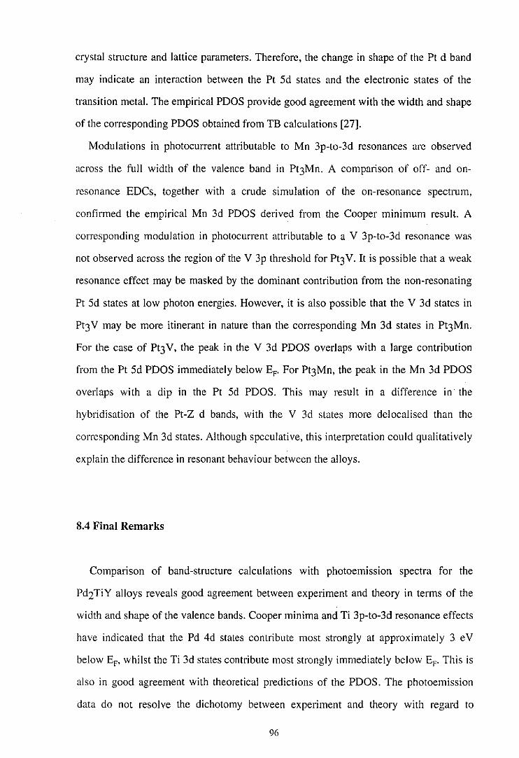
crystal stmcture and lattice parameters. Therefore, the change in shape of the Pt d band
may indicate an interaction between the Pt 5d states and the electronic states of the
transition metal. The empirical PDOS provide good agreement with the width and shape
of the corresponding PDOS obtained from TB calculations [27].
Modulations in photocurrent attributable to Mn 3p-to-3d resonances are observed
across the full width of the valence band in Pt3Mn. A comparison of off- and on
resonance EDCs, together with a crude simulation of the on-resonance spectmm,
confirmed the empirical Mn 3d PDOS derived from the Cooper minimum result. A
corresponding modulation in photocurrent attributable to a V 3p-to-3d resonance was
not observed across the region of the V 3p threshold for Pt3 V. It is possible that a weak
resonance effect may be masked by the dominant contribution from the non-resonating
Pt 5d states at low photon energies. However, it is also possible that the V 3d states in
Pt3 V may be more itinerant in nature than the corresponding Mn 3d states in Pt3Mn.
For the case of Pt3 V, the peak in the V 3d PDOS overlaps with a large contribution
from the Pt 5d PDOS immediately below EF. For Pt3Mn, the peak in the Mn 3d PDOS
overlaps with a dip in the Pt 5d PDOS. This may result in a difference in the
hybridisation of the Pt-Z d bands, with the V 3d states more delocalised than the
corresponding Mn 3d states. Although speculative, this interpretation could qualitatively
explain the difference in resonant behaviour between the alloys.
SA Final Remarks
Comparison of band-structure calculations with photoemission spectra for the
Pd2TiY alloys reveals good agreement between experiment and theory in terms of the
width and shape of the valence bands. Cooper minima and Ti 3p-to-3d resonance effects
have indicated that the Pd 4d states contribute most strongly at approximately 3 eV
below EF, whilst the Ti 3d states contribute most strongly immediately below EF. This is
also in good agreement with theoretical predictions of the PDOS. The photoemission
data do not resolve the dichotomy between experiment and theory with regard to
96

magnetic order in these materials. However, the photoemission measurements do
confirm that the band-structure calculations provide a valid representation of the valence
electronic structure.
From the results obtained in this study, it is clear that the Anderson model [32] for
local moment formation, consisting of a localised virtual bound state, is not applicable
to the X2MnY and Pt3Z alloys. Resonant photoemission indicates that the Mn 3d states
in Pt3Mn and the X2Mn Y series disperse across the full width of the valence band.
Empirical determination of the PDOS for Pd2MnSn indicates that the Mn 3d states are
degenerate with a high density of Pd 4d states. The empirically determined PDOS for
Pt3 V and Pt3Mn also indicate that the Pt 5d and transition metal 3d states completely
overlap. This is consistent with the model for local moment formation comprising
itinerant electrons within a hybridised, delocalised d band [20]. Kohn-Korringa
Rostocker (KKR) calculations of the electronic structure of dilute alloys indicate that,
for 3d metal impurities in Ag, virtual bound states are formed in accordance with the
Anderson model, but for Mn in Cu, the Mn d states are modified by interaction with
neighbouring host d orbitals [134]. The resulting calculation of the Mn 3d PDOS is very
similar to that reported by Kubler et al. [20] for Cu2MnAI.
Some anomalies with respect to resonant participation are evident. For Pt3Mn, a
clear, albeit weak 3p-to-3d resonance is observed, whilst for Pt3 V no clear modulation
is evident across the region of the 3p threshold. For Co2MnSn, variations in resonant
structure are observed across the band, with states at higher binding energies exhibiting
modulations in photocurrent close to those expected in the limit of no hybridisation.
This suggests differences in localisation of the transition metal 3d states that are difficult
to account for within the framework of a completely delocalised, common d band.
Band-structure calculations indicate that the minority-spin Mn 3d states are almost
completely unoccupied in the X2MnY and Pt3Mn alloys, whilst the corresponding
majority-spin states are completely occupied [16-20, 25, 27]. To determine the
occupancy of the spin-split states in these alloys, spin-resolved photoemission would
need to be employed [57]. For alloys such as Pd2MnSn and Pt3Mn, the contribution
from Pd and Pt states can be considered negligible at excitation energies corresponding
97

to the respective Cooper minima. Consequently, if minority-spin electrons are almost
completely excluded from Mn sites, then polarisations close to unity should be observed
across the valence bands of the Pd and Pt alloys at 130 and 150 eV respectively.
However, such measurements would be problematical due to the difficulties of in situ
reversible magnetisation of the samples.
98

References
[I] F. Heusler, Verh. Deutsch Phys. Gese/5, 219, (1903).
[2] P.J. Webster and R.S. Tebble, Phi!. Mag. 16,347, (1967).
[3] P.J. Webster,J. Phys. Chem. Solids 32, 1221, (1971).
[4] E.P. Wohlfarth and K.H.J. Buschow (eds.), Ferromagnetic Materials, Vol. 4,
p287-290, (Elsevier, Amsterdam, 1988) and references therein.
[5] K.U. Neumann, J. Crangle, J.G. Smith, N.K. Zayer and K.R.A. Ziebeck, J. Mag.
Mag. Mat. 137,264, (1994).
[6] K.U. Neumann, J. Crangle, R.K. Kremer, N.K. Zayer and K.R.A. Ziebeck, J. Mag.
Mag. Mat. 127, 47, (1993).
[7] K.U. Neumann, J. Crangle, M.D. Crapper, J.G. Smith, N.K. Zayer and K.R.A.
Ziebeck, J. Mag. Mag. Mat. 146, 30, (1995).
[8] H. Wright, P. Weightman, P.T. Andrews, W. Folkerts, C.F.J. Flipse, G.A.
Sawatzky, D. Norman and H. Padmore, Phys. Rev. B 35,519, (1987).
[9] S. Lobus, R. Courths, S. Halilov, H. Gollisch and R. Feder, Surf. Rev. Lett. 3,
1749, (1996).
[10] R. Kuentzler, Physics of Transition Metals, p397, Inst. Phys. Conf. Ser. 55,
(1980).
[I!] M. Kawakami and T. Goto, J. Phys. Soc. Japan 46, 1492, (1979).
[ 12] S.K. Burke, B.D. Rain ford, D.E.G. Williams, P.J. Brown and D.A. Hukin, J. Mag.
Mag. Mat. 15-18,505, (1980).
[ 13] B. Antonini, F. Lucari, F. Menzinger and A. Paoletti, Phys. Rev. 187, 611, (1969).
[14] G.E. Bacon and J. Crangle, Proc. Phys. Soc. A 272, 387, (1963).
[ 15] F. Menzinger and A. Paoletti, Phys. Rev. 143, 365, ( 1966).
[16] S. Ishida, J. Ishida, S. Asano and J. Yamashita, J. Phys. Soc. Japan 45, 1239,
(1978).
[ 17] S. Ishida, S. Akazawa, Y. Kubo and J. Ishida, J. Phys. F: Met. Phys. 12, 1111,
(1982).
[ 18] S. Ishida, Y. Kubo, J. Ishida and S. Asano, J. Phys. Soc. Japan 48, 814, ( 1980).
99
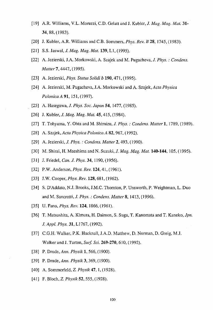
[19] A.R. Williams, V.L. Moruzzi, C.D. Gelatt and J. Kubler, J. Mag. Mag. Mat. 3I-
34, 88, ( 1983).
[20] J. Kubler, A.R. Williams and C.B. Sommers, Phys. Rev. B 28, 1745, ( 1983).
[21] S.S. Jaswal, J. Mag. Mag. Mat. 139, L1, ( 1995).
[22] A. Jezierski, J.A. Morkowski, A. Szajek and M. Pugacheva, J. Phys. : Condens.
Matter7,4447, (1995).
[23] A. Jezierski, Phys. Status Solidi b 190, 471, (1995).
[24] A. Jezierski, M. Pugacheva, J.A. Morkowski and A. Szajek, Acta Physica
Polonica A 91, 151, (1997).
[25] A. Hasegawa, J. Phys. Soc. Japan 54, 1477, (1985).
[26] J. Kubler, J. Mag. Mag. Mat. 45,415, (1984).
[27] T. Tohyama, Y. Ohta and M. Shimizu, J. Phys.: Condens. Matter I, 1789, (1989).
[28] A. Szajek, Acta Physica Polonica A 82, 967, ( 1992).
[29] A. Jezierski, J. Phys. : Condens. Matter 2, 493, ( 1990).
[30] M. Shirai, H. Maeshima and N. Suzuki, J. Mag. Mag. Mat. 140-144, 105, (1995).
[31] J. Friedel, Can. J. Phys. 34, 1190, (1956).
[32] P.W. Anderson, Phys. Rev. 124, 41, (1961 ).
[33] J.W. Cooper, Phys. Rev. I28, 681, (1962).
[34] S. D'Addato, N.J. Brooks, J.M.C. Thornton, P. Unsworth, P. Weightman, L. Duo
and M. Sancrotti, J. Phys. : Condens. Matter 8, 1413, ( 1996).
[35] U. Fano, Phys. Rev. I24, 1866, (1961).
[36] T. Matsushita, A. Kimura, H. Daimon, S. Suga, T. Kanomata and T. Kaneko, Jpn.
J. Appl. Phys. 31, L1767, (1992).
[37] C.G.H. Walker, P.K. Hucknall, J.A.D. Matthew, D. Norman, D. Greig, M.J.
Walker and J. Turton, Suif. Sci. 269-270,610, (1992).
[38] P. Drude, Ann. Physik I, 566, (1900).
[39] P. Drude, Ann. Physik 3, 369, (1900).
[40] A. Sommerfeld, Z. Physik 47, I, (1928).
[41] F. Bloch, Z. Physik 52, 555, (1928).
100

[42] N.W. Ashcroft and N.D. Mermin, Solid State Physics, (Saunders College,
Philadelphia, 1976).
[43] J. Ziman, Principles of the Theory of Solids, (Cambridge, 1972).
[44] W.A. Harrison, Phys. Rev. 118, 1182, (1960).
[45] J.C. Slater, Phys. Rev. 51,846, (1937).
[46] J.C. Slater, Phys. Rev. 92,603, (1937).
[47] C. Herring and A.G. Hill, Phys. Rev. 58, 132, (1940).
[ 48] W.A. Harrison, Electronic Structure and the Properties of Solids, (Freeman, San
Francisco, 1980).
[ 49] H. Hertz, Ann. Physik 31, 983, ( 1887).
[50] J.J. Thompson, Phi!. Mag. 44,293, (1897).
[51] P. Lenard, Ann. Physik 2, 359, (1900).
[52] J.J. Thompson, Phi!. Mag. 48,547, (1899).
[53] A. Einstein, Ann. Physik 17, 132, (1905).
[54] P. Lukirsky and S. Prilezaev, Z. Physik 49,236, (1928).
[55] M.P. Seah and W.A. Dench, Suif. Inteiface Anal. 1, 2, (1979).
[56] S.D. Kevan (ed.), Angle-Resolved Photoemission: Theory and Current
Applications, (Elsevier, Amsterdam, 1992).
[57] P.D. Johnson, Nucl. Instr. and Meth. A 319, 264, (1992).
[58] C.M. Schneider and J. Kirschner, Crit. Rev. Solid State and Mater. Sci. 20, 179,
(1995).
[59] S. Hufner, Photoelectron Spectroscopy: Principles and Applications, (Springer
Verlag, Berlin, 1996).
[60] E.O. Kane, Phys. Rev. Lett. 12, 97, (1964).
[61] N.V. Smith, M.M. Traum, and F.J. DiSalvo, Solid State Commun. 15,211,
(1974).
[62] B. Feuerbacher, B. Fitton and R.F. Willis, Photoemission and the Electronic
Properties of Surfaces, (Wiley, New York, 1978) and references therein.
[63] N.F. Mott, Proc. R. Soc. A 135,429, ( 1932).
[64] M. Campagna, J. Vac. Sci. Technol. A 3, 1491, ( 1985).
101

[65] R. Rave, H. Hopster and R. Clauberg, Phys. Rev. Lett. 50, 1623, ( 1983).
[66] Y.B. Xu, C.G.H. Walker, D. Greig, E.A. Seddon, I.W. Kirkman, F.M. Quinn and
J.A.D. Matthew, J. Phys. : Condens. Matter 8, 1567, (1996).
[67] Y.B. Xu, D. Greig, E.A. Seddon and J.A.D. Matthew, Phys. Rev. B 55, 11442,
(1997).
[68] H. Claus and K. Ulmer, Z. Physik 173,462, (1963).
[69] J.K. Lang and Y. Baer, Rev. Sci.lnstr. 50,221, (1979).
[70] G. Denninger, V. Dose and H. Scheidt, Appl. Phys. 18, 375, (1979).
[71] K. Desinger, V. Dose, M. Glob! and H. Scheidt, Solid State Commun. 49,479,
(1984).
[72] W. Altmann, V. Dose, A. Goldmann, U. Kolac and J. Rogozik, Phys. Rev. B 29,
3015, (1984).
[73] F.J. Himpsel and T. Fauster, J. Vac. Sci. Technol. A 2, 815, (1984).
[74] S. Hufner, G.K. Wertheim, and J.H. Wernick, Phys. Rev. B 8, 4511, ( 1973).
[75] S. Hufner, G.K. Wertheim and J.H. Wernick, Solid State Commun. 17, 1585,
(1975).
[76] D. Van der Mare!, G.A. Sawatzky, F.U. Hillebrecht, Phys. Rev. Lett. 53, 206,
(1984).
[77] H. Hochst, P. Steiner and S. Hufner, J. Mag. Mag. Mat. 6, !59, (1977).
[78] P. Steiner, H. Hochst, W. Steffen and S. Hufner, Z. Physik B 38, 191, (1980).
[79] P. Steiner, H. Hochst and S. Hufner, J. Phys. F: Met. Phys. 7, L I 05, (1977).
[80] H. Hochst, P. Steiner and S. Hufner, Z. Physik B 38,201, (1980).
[81] W. Folkerts, D. Van der Mare!, C. Haas, G.A. Sawatzky, D. Norman, H. Padmore,
H. Wright and P. Weightman, J. Phys. F: Met. Phys. 17,657, (1987).
[82] R.J. Cole, J.A. Evans, L. Duo, A.D. Laine, P.S. Fowles, P. Weightman, G.
Mondio, and D. Norman, Phys. Rev. B 46, 3747, (1992).
[83] R.J. Cole, P. Weightman, D.R. Jennison and E.B. Stechel, J. Electron Spectrosc.
68, 139, (1994).
[84] G. Meng, R. Claessen, F. Reinert, R. Zimmermann, P. Steiner and S. Hufner, J.
Phys. Condens. Matter 8, 5569, (1996).
102
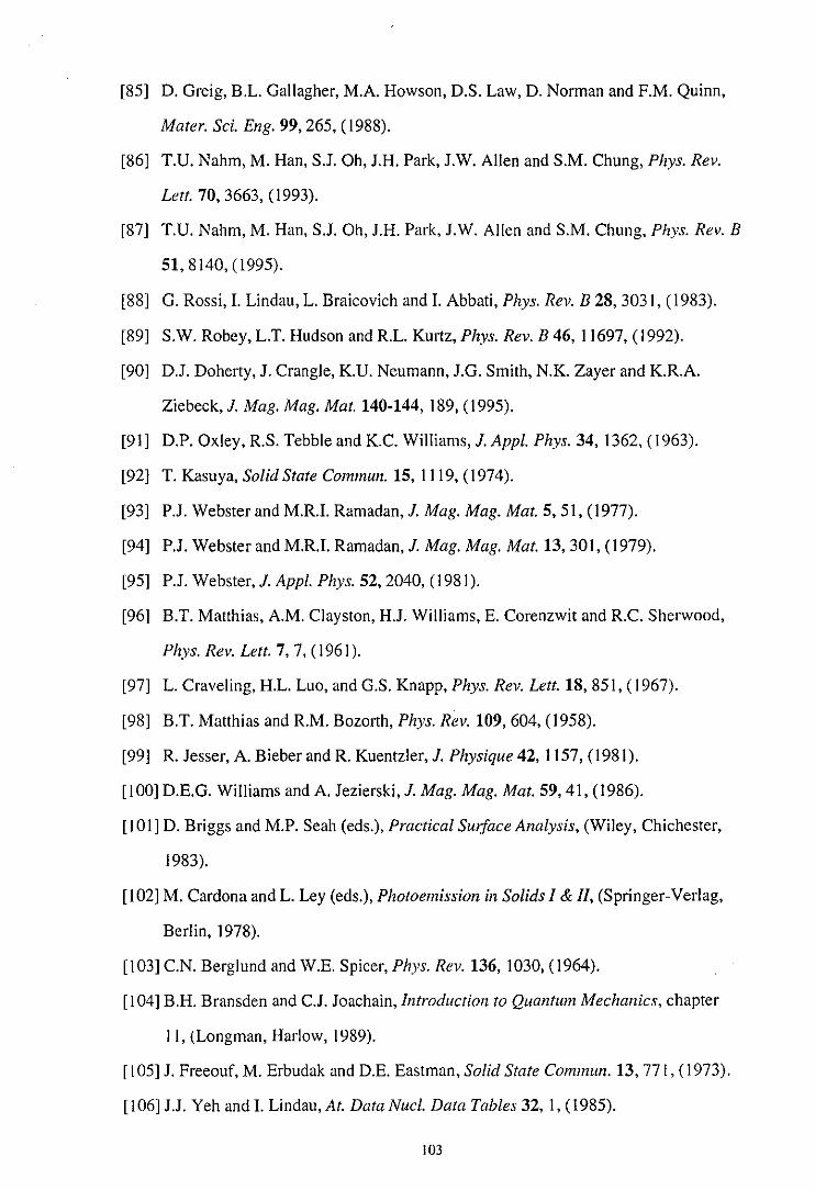
[85] D. Greig, B.L. Gallagher, M.A. Howson, D.S. Law, D. Norman and F.M. Quinn,
Mater. Sci. Eng. 99,265, ( 1988).
[86] T.U. Nahm, M. Han, S.J. Oh, J.H. Park, J.W. Alien and S.M. Chung, Phys. Rev.
Lett. 70, 3663, ( 1993).
[87] T.U. Nahm, M. Han, S.J. Oh, J.H. Park, J.W. Alien and S.M. Chung, Phys. Rev. B
51,8140, (1995).
[88] G. Rossi, I. Lindau, L. Braicovich and I. Abbati, Phys. Rev. B 28, 3031, ( 1983).
[89] S.W. Robey, L.T. Hudson and R.L. Kurtz, Phys. Rev. B 46, 11697, ( 1992).
[90] D.J. Doherty, J. Crangle, K.U. Neumann, J.G. Smith, N.K. Zayer and K.R.A.
Ziebeck, J. Mag. Mag. Mat. 140-144, 189, (1995).
[91] D.P. Oxley, R.S. Tebble and K.C. Williams, J. Appl. Phys. 34, 1362, ( 1963).
[92] T. Kasuya, Solid State Commun. 15, 1119, ( 1974).
[93] P.J. Webster and M.R.I. Ramadan, J. Mag. Mag. Mat. 5, 51, ( 1977).
[94] P.J. Webster and M.R.I. Ramadan, J. Mag. Mag. Mat. 13,301, (1979).
[95] P.J. Webster, J. Appl. Phys. 52, 2040, (1981 ).
[96] B.T. Matthias, A.M. C1ayston, H.J. Williams, E. Corenzwit and R.C. Sherwood,
Phys. Rev. Lett. 7, 7, (1961).
[97] L. Craveling, H.L. Luo, and G.S. Knapp, Phys. Rev. Lett. 18, 851, ( 1967).
[98] B.T. Matthias and R.M. Bozorth, Phys. Rev. 109,604, (1958).
[99] R. Jesser, A. Bieber and R. Kuentzler, J. Physique 42, 1157, (1981 ).
[100] D.E.G. Williams and A. Jezierski, J. Mag. Mag. Mat. 59, 41, (1986).
[101] D. Briggs and M.P. Seah (eds.), Practical Surface Analysis, (Wiley, Chichester,
1983).
[102] M. Cardona and L. Ley (eds.), Photoemission in Solids I & Il, (Springer-Verlag,
Berlin, 1978).
[I 03] C.N. Berglund and W.E. Spicer, Phys. Rev. 136, 1030, (1964).
[104] B.H. Bransden and C.J. Joachain, Introduction to Quantum Mechanics, chapter
11, (Longman, Harlow, 1989).
[ 1 05] J. Freeouf, M. Erbudak and D.E. Eastman, Solid State Commun. 13, 771, ( 1973).
[1 06] J.J. Yeh and I. Lindau, At. Data Nucl. Data Tables 32, I, (1985).
103

[I 07] F. Herman and S. Skill man, Atomic Structure Calculations, (Prentice-Hall, New
Jersey, 1963).
[I 08] D.J. Kennedy and S.T Manson, Phys. Rev. A 5, 227, (1972).
[I 09] B.H. Henke, Phys. Rev. A 6, 94, ( 1972).
[110] T. Kashiwakura, S. Suzuki, T. Okane, S. Sato, T. Kinoshita, A. Kakizaki, T. Ishii,
Y. Isikawa, H. Yamagami and A. Hasegawa, Phys. Rev. B 47, 6885, ( 1993).
[Ill] L.C. Davis, Phys. Rev. B 25,2912, (1982).
[ 112] A. Kakizaki, K. Sugeno, T. Ishii, H. Sugawara, I. Nagakura and S. Shin, Phys.
Rev. B 28, I 026, (1983).
[ 113] M. I wan, F.J. Himpsel and D.E. Eastman, Phys. Rev. Lett. 43, 1829, (1979).
[ 114] D. Chandesris, J. Lecante and Y. Petroff, Phvs. Rev. B 27, 2630, ( 1983).
[ 115] H. Kato, T. Ishii, S. Masuda, Y. Harada, T. Miyano, T. Komeda, M. Onchi and Y.
Sakisaka, Phys. Rev. B 32, 1992, ( 1985).
[ 116] H. Winick (ed.), Synchrotron Radiation Sources: A Primer, (World Scientific,
Singapore, 1994 ).
[ 117] P. Bailey and F.M. Quinn, Daresbury Laboratory Technical Memorandum,
DLISCVTM94E, (1993).
[ 118] T.S. Turner and D. Teehan, Daresbury Laboratory Technical Memorandum,
DL/SCVTM85E, ( 1985).
[I 19] D.A. Shirley, Phys. Rev. B 5, 4 709, (1972).
[ 120] J.C. Fuggle and N. Martensson, J. Electron Spectrosc. 21, 275, ( 1980).
[ 121] L.E. Davis, N.C. MacDona1d, P.W. Palmberg, G.E. Riach and R.E. Weber,
Handbook of Auger Electron Spectroscopy, (Physical Electronics Industries Inc.,
Minnesota, 1976).
[122] A. Szytula, T. Czeppe and J. Stoch, J. Less-Common Met. 159, L5, (1990).
[ 123] J.S. Kang, J.G. Park, C. G. Olson, S.J. Youn and B.I. Min, J. Phys. : Condens.
Matter 7, 3789, (1995).
[124] E. Schmidt, H. Schroder, B. Sonntag, H. Voss and H.E. Wetzel, J. Phys. B: At.
Mol. Phys. 18, 79, (1985).
104

[ 125] A.J. Liddiard, M.D. Crapper, P.K. Hucknall, M. Petty, P.A. Skull, N.D. Telling
and R.B. Pate!, Surf Sci. 331-333, 794, ( 1995).
[ 126] A. Amamou and R. Kuentzler, Solid State Commun. 43, 423, ( 1982).
[127] A.J. Liddiard, R.B. Pate! and M.D. Crapper, Sur]: Sci. 307-309, 450, ( 1994).
[ 128] D.A. Papaconstantopoulos, Handbook of the Banc/ Structure of Elemental Solids,
(New York, Plenum, 1986).
[129] H. Winter, P.J. Durham, W.M. Temmerman and G.M. Stocks, Phys. Rev. B 33,
2370, (1986).
[130] H. Sugawara, A. Kakizaki, I. Nagakura and T. Ishii, J. Phys. F: Met. Phys. 12,
2929, (1982).
[ 131] J.A. Applebaum and D.R. Hamann, Solid State Commun. 27, 881, ( 1978).
[132] P. Steiner, S. Hufner, A.J. Freeman and D. Wang, Solid State Commun. 44,619,
( 1982).
[133] P.H. Citrin, G.K. Wertheim and Y. Baer, Phys. Rev. B 21,3160, (1983).
[ 134] R. Podloucky, R. Zeller and P.H. Dederichs, Phys. Rev. B 22, 5777, ( 1980).
105