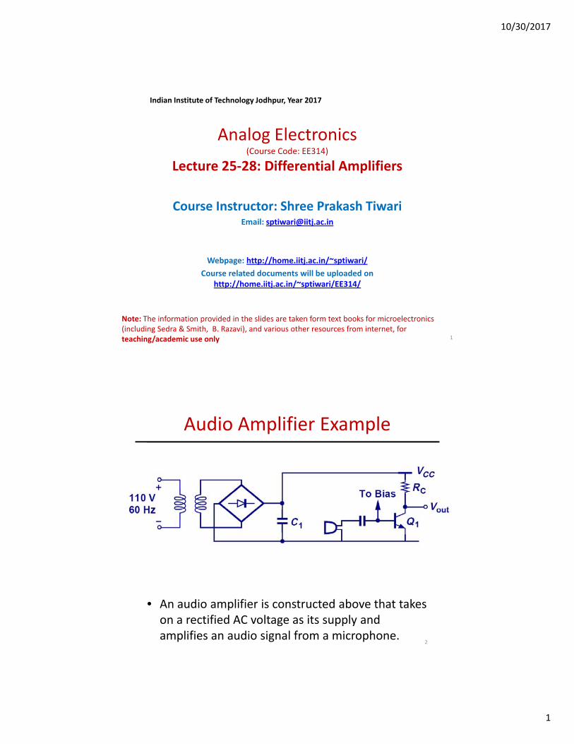
audio amplifier example - indian institute of technology...
TRANSCRIPT
10/30/2017
1
Analog Electronics(Course Code: EE314)
Lecture 25‐28: Differential Amplifiers
Indian Institute of Technology Jodhpur, Year 2017
Course Instructor: Shree Prakash TiwariEmail: [email protected]
Webpage: http://home iitj ac in/~sptiwari/Webpage: http://home.iitj.ac.in/~sptiwari/
Course related documents will be uploaded on http://home.iitj.ac.in/~sptiwari/EE314/
1
Note: The information provided in the slides are taken form text books for microelectronics (including Sedra & Smith, B. Razavi), and various other resources from internet, for teaching/academic use only
Audio Amplifier Example
2
• An audio amplifier is constructed above that takes on a rectified AC voltage as its supply and amplifies an audio signal from a microphone.

10/30/2017
2
“Humming” Noise in Audio Amplifier Example
3
• However, VCC contains a ripple from rectification that leaks to the output and is perceived as a “humming” noise by the user.
Supply Ripple Rejection
A
invYX
rY
rinvX
vAvv
vv
vvAv
4
• Since both node X and Y contain the ripple, their difference will be free of ripple.
10/30/2017
3
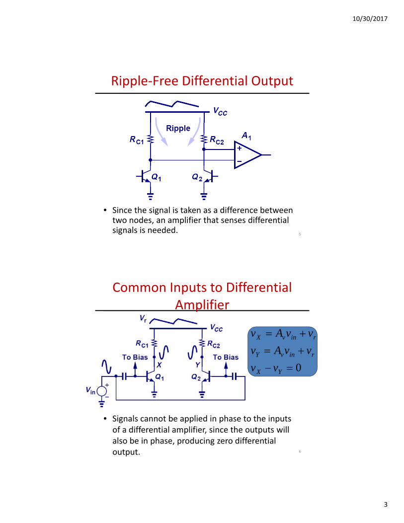
Ripple‐Free Differential Output
5
• Since the signal is taken as a difference between two nodes, an amplifier that senses differential signals is needed.
Common Inputs to Differential Amplifier
rinvX vvAv
0
YX
rinvY
vv
vvAv
6
• Signals cannot be applied in phase to the inputs of a differential amplifier, since the outputs will also be in phase, producing zero differential output.

10/30/2017
4
Differential Inputs to Differential Amplifier
rinvX vvAv
invYX
rinvY
vAvv
vvAv
2
7
• When the inputs are applied differentially, the outputs are 180° out of phase; enhancing each other when sensed differentially.
Differential Signals
• A pair of differential signals can be generated, th b t f
8
among other ways, by a transformer.
• Differential signals have the property that they share the same average value to ground and are equal in magnitude but opposite in phase.
10/30/2017
5
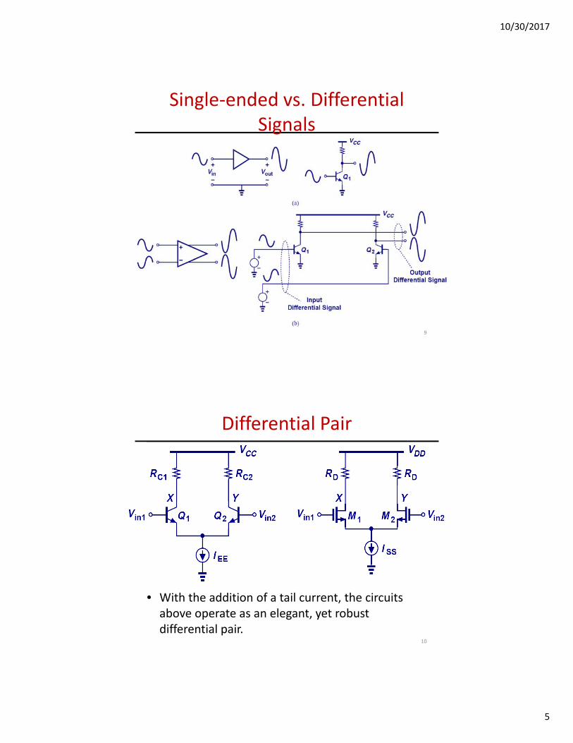
Single‐ended vs. Differential Signals
9
Differential Pair
10
• With the addition of a tail current, the circuits above operate as an elegant, yet robust differential pair.

10/30/2017
6
Common‐Mode Response
2
221
21
EECCCYX
EECC
BEBE
IRVVV
III
VV
11
2
Common‐Mode Rejection
12
• Due to the fixed tail current source, the input common‐mode value can vary without changing the output common‐mode value.
10/30/2017
7
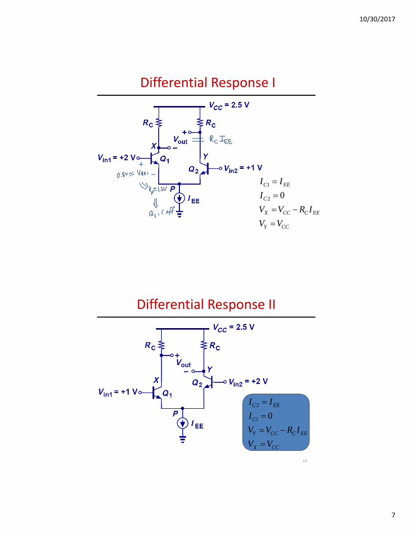
Differential Response I
EEC II 1
CCY
EECCCX
C
EEC
VV
IRVV
I
02
1
Differential Response II
EEC II 2
14
CCX
EECCCY
C
VV
IRVV
I
01
10/30/2017
8
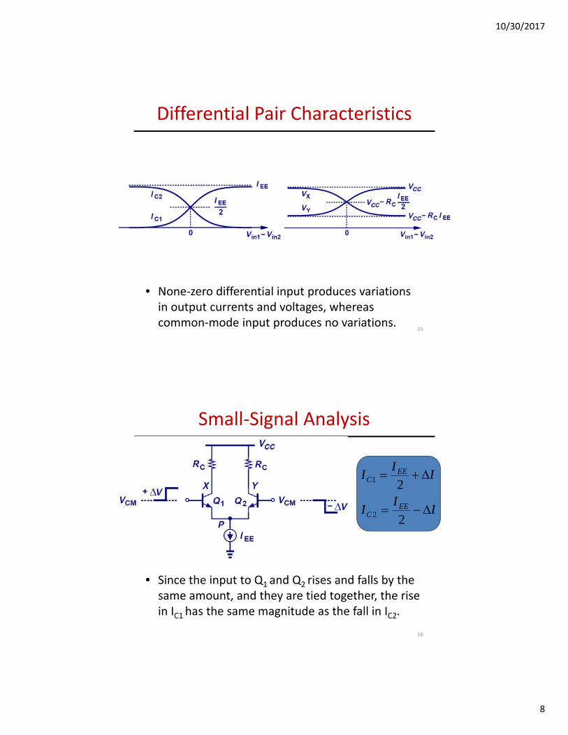
Differential Pair Characteristics
15
• None‐zero differential input produces variations in output currents and voltages, whereas common‐mode input produces no variations.
Small‐Signal Analysis
II
I EEC 1
II
I
II
EEC
C
2
2
2
1
16
• Since the input to Q1 and Q2 rises and falls by the same amount, and they are tied together, the rise in IC1 has the same magnitude as the fall in IC2.
10/30/2017
9
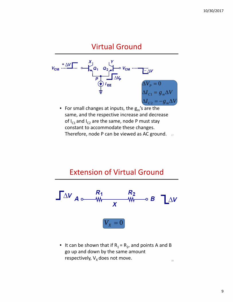
Virtual Ground
VgI
VgI
V
mC
mC
P
2
1
0
17
• For small changes at inputs, the gm’s are the same, and the respective increase and decrease of IC1 and IC2 are the same, node P must stay constant to accommodate these changes. Therefore, node P can be viewed as AC ground.
Extension of Virtual Ground
0XV
18
• It can be shown that if R1 = R2, and points A and B go up and down by the same amount respectively, VX does not move.
10/30/2017
10
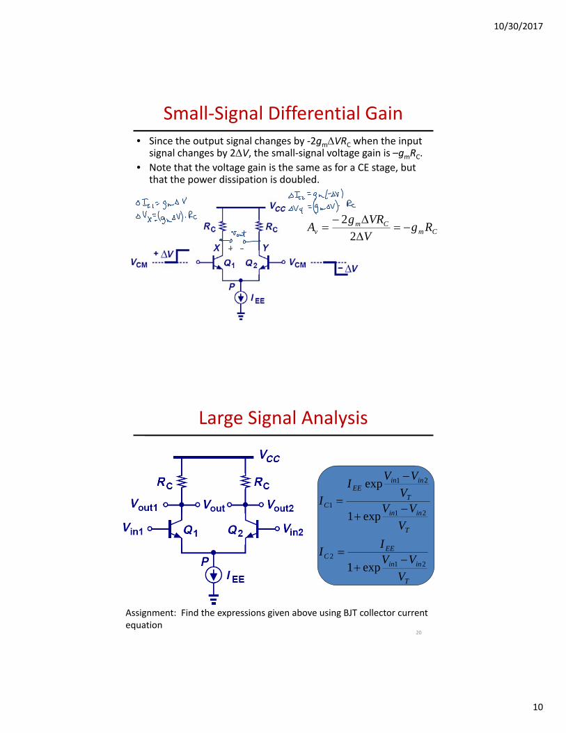
Small‐Signal Differential Gain• Since the output signal changes by ‐2gmVRC when the input
signal changes by 2V, the small‐signal voltage gain is –gmRC.
• Note that the voltage gain is the same as for a CE stage, but g g g ,that the power dissipation is doubled.
CmCm
v RgV
VRgA
2
2
Large Signal Analysis
VV
EEC
T
inin
T
ininEE
C
VVI
I
V
VVV
VVI
I
2
21
21
1
exp1
exp
20
T
inin
V
VV 21exp1
Assignment: Find the expressions given above using BJT collector current equation
10/30/2017
11
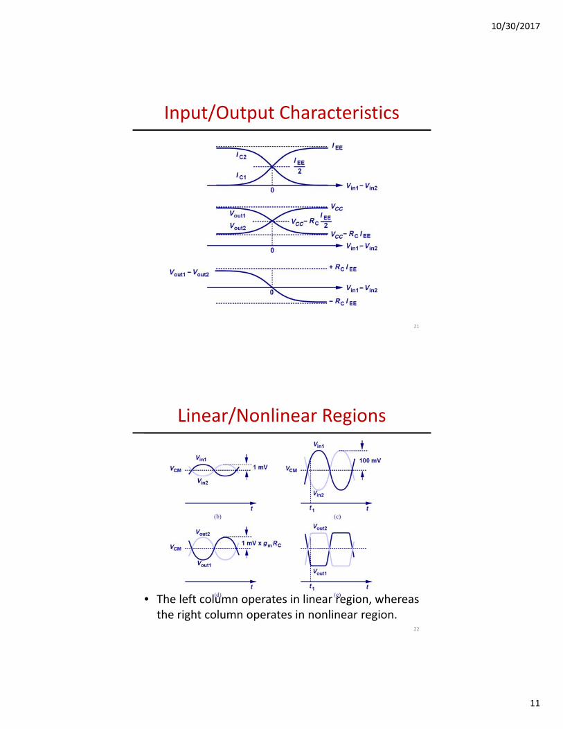
Input/Output Characteristics
21
Linear/Nonlinear Regions
22
• The left column operates in linear region, whereas the right column operates in nonlinear region.
10/30/2017
12
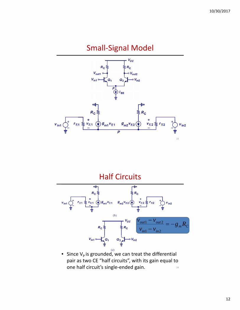
Small‐Signal Model
23
Half Circuits
Cminin
outout Rgvv
vv
21
21
24
• Since VP is grounded, we can treat the differential pair as two CE “half circuits”, with its gain equal to one half circuit’s single‐ended gain.
10/30/2017
13
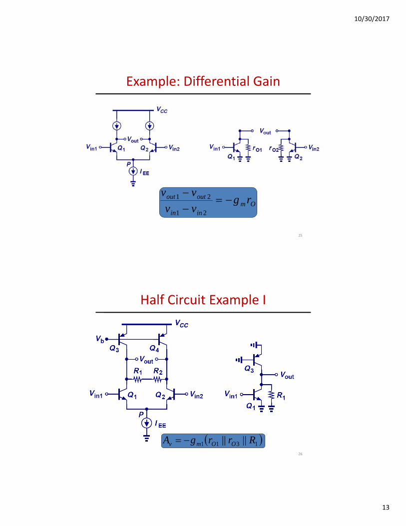
Example: Differential Gain
25
Ominin
outout rgvv
vv
21
21
Half Circuit Example I
26
1311 |||| RrrgA OOmv
10/30/2017
14
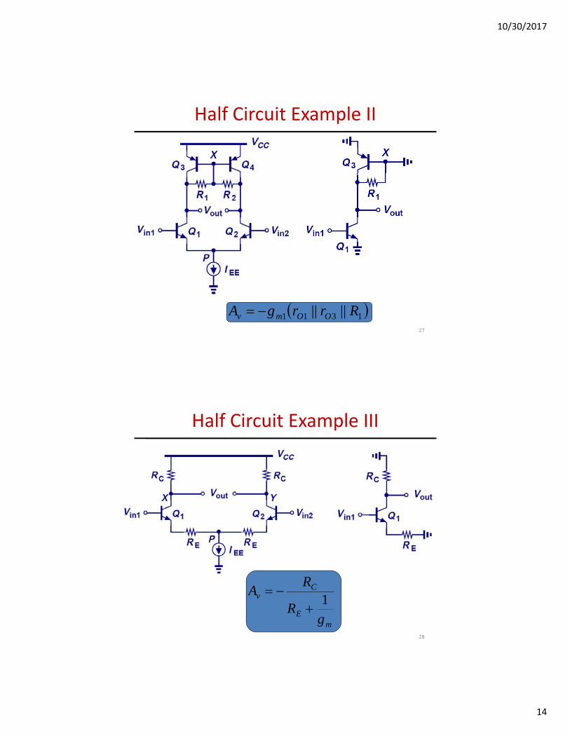
Half Circuit Example II
27
1311 |||| RrrgA OOmv
Half Circuit Example III
28
mE
Cv
gR
RA
1
10/30/2017
15
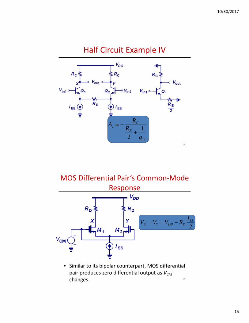
Half Circuit Example IV
29
m
E
Cv
g
RR
A1
2
MOS Differential Pair’s Common‐Mode Response
2SS
DDDYX
IRVVV
30
• Similar to its bipolar counterpart, MOS differential pair produces zero differential output as VCM
changes.
10/30/2017
16
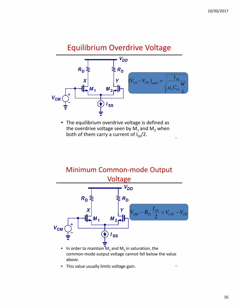
Equilibrium Overdrive Voltage
L
WC
IVV
oxn
SSequilTHGS
31
• The equilibrium overdrive voltage is defined as the overdrive voltage seen by M1 and M2 when both of them carry a current of ISS/2.
Minimum Common‐mode Output Voltage
THCMSS
DDD VVI
RV 2
32
• In order to maintain M1 and M2 in saturation, the common‐mode output voltage cannot fall below the value above.
• This value usually limits voltage gain.

10/30/2017
17
Differential Response
33
Small‐Signal Response
PV 0
Dmv RgA
34
• Similar to its bipolar counterpart, the MOS differential pair exhibits the same virtual ground node and small signal gain.
10/30/2017
18
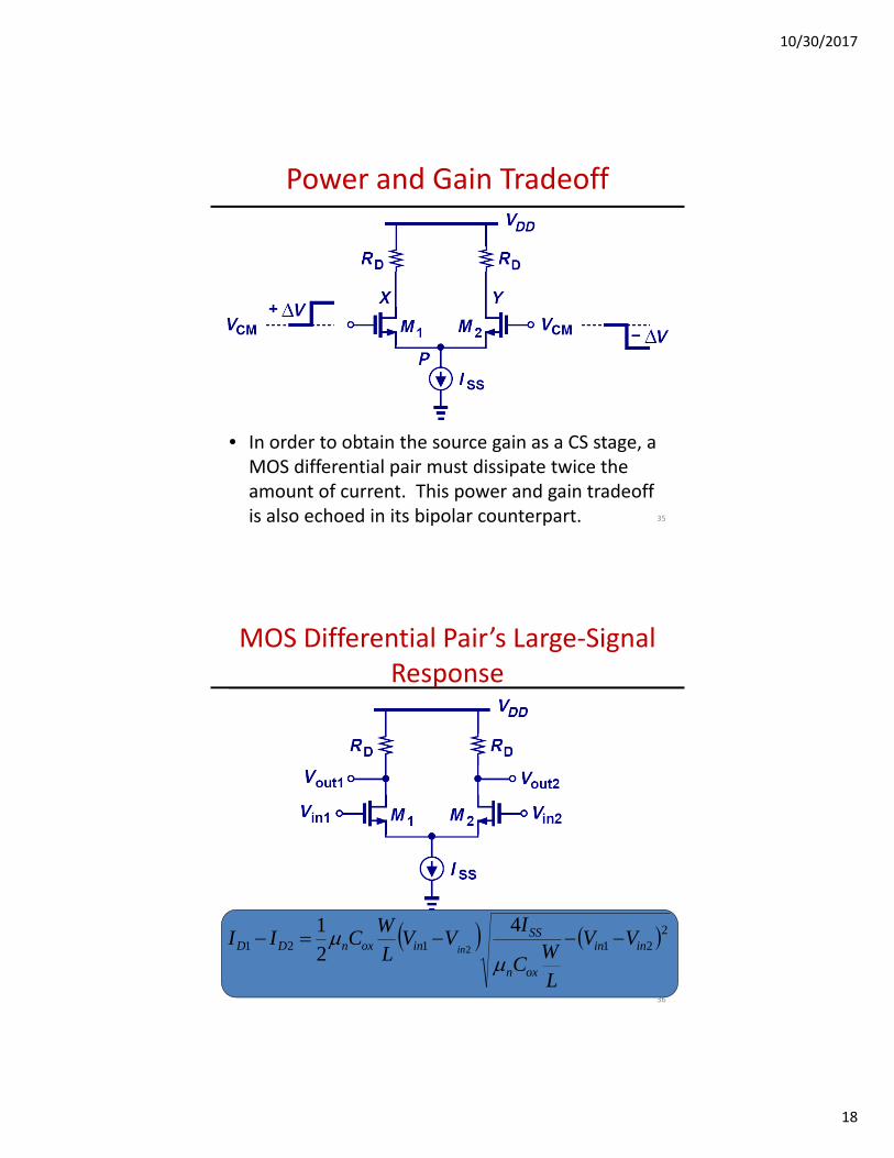
Power and Gain Tradeoff
35
• In order to obtain the source gain as a CS stage, a MOS differential pair must dissipate twice the amount of current. This power and gain tradeoff is also echoed in its bipolar counterpart.
MOS Differential Pair’s Large‐Signal Response
36
221121
4
2
12 inin
oxn
SSinoxnDD VV
L
WC
IVV
L
WCII
in
10/30/2017
19
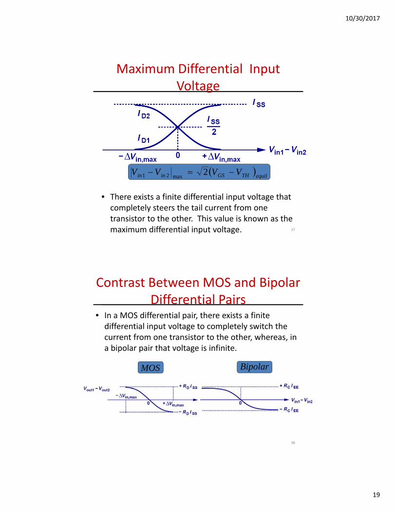
Maximum Differential Input Voltage
equilTHGSinin VVVV 2max21
37
• There exists a finite differential input voltage that completely steers the tail current from one transistor to the other. This value is known as the maximum differential input voltage.
Contrast Between MOS and Bipolar Differential Pairs
• In a MOS differential pair, there exists a finite differential input voltage to completely switch the
f h h hcurrent from one transistor to the other, whereas, in a bipolar pair that voltage is infinite.
MOS Bipolar
38
10/30/2017
20
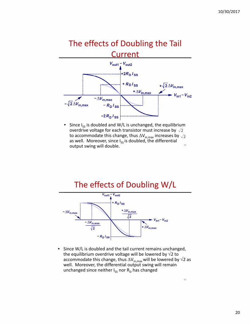
The effects of Doubling the Tail Current
39
• Since ISS is doubled and W/L is unchanged, the equilibrium overdrive voltage for each transistor must increase by to accommodate this change, thus Vin,max increases by as well. Moreover, since ISS is doubled, the differential output swing will double.
2
2
The effects of Doubling W/L
Si W/L i d bl d d th t il t i h d
40
• Since W/L is doubled and the tail current remains unchanged, the equilibrium overdrive voltage will be lowered by 2 to accommodate this change, thus Vin,maxwill be lowered by 2 as well. Moreover, the differential output swing will remain unchanged since neither ISS nor RD has changed
10/30/2017
21
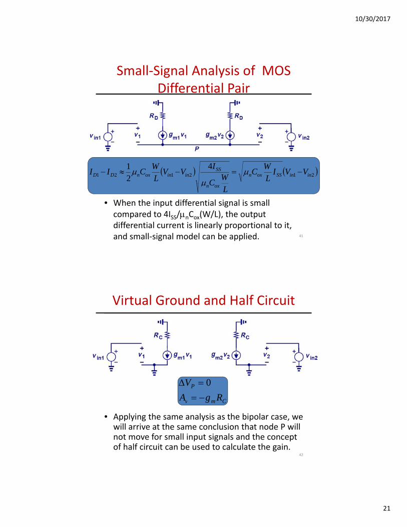
Small‐Signal Analysis of MOS Differential Pair
212121
4
2
1ininSSoxn
SSininoxnDD VVI
L
WC
WC
IVV
L
WCII
41
• When the input differential signal is small compared to 4ISS/nCox(W/L), the output differential current is linearly proportional to it, and small‐signal model can be applied.
oxn LC
Virtual Ground and Half Circuit
Cmv
P
RgA
V
0
42
• Applying the same analysis as the bipolar case, we will arrive at the same conclusion that node P will not move for small input signals and the concept of half circuit can be used to calculate the gain.
Cmv
10/30/2017
22
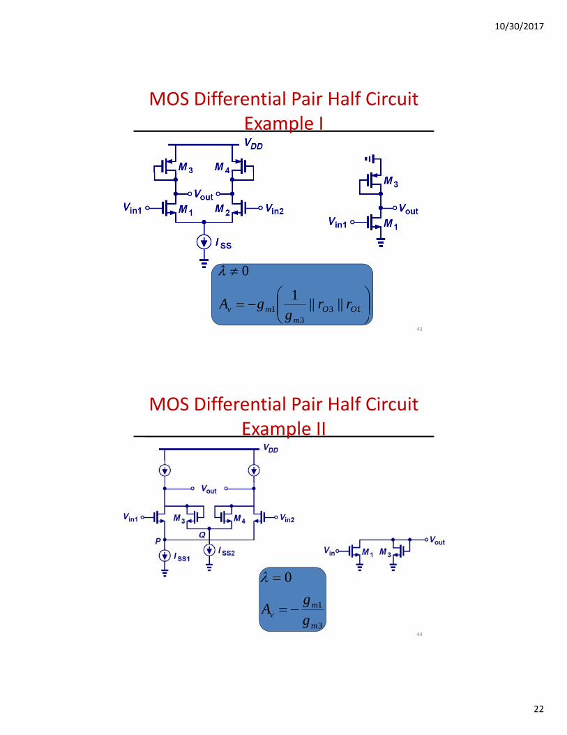
MOS Differential Pair Half Circuit Example I
43
133
1 ||||1
0
OOm
mv rrg
gA
MOS Differential Pair Half Circuit Example II
44
3
1
0
m
mv g
gA
10/30/2017
23
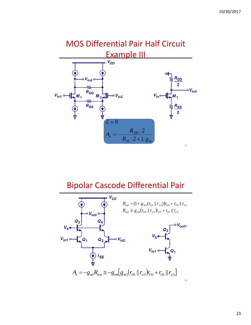
MOS Differential Pair Half Circuit Example III
45
mSS
DDv gR
RA
12
2
0
Bipolar Cascode Differential Pair
313313
313313
||||
||)]||(1[
rrrrrgR
rrrrrgR
OOOt
OOOmout
313313 |||| rrrrrgR OOOmout
46
31331311 |||| rrrrrggRgA OOOmmoutmv
10/30/2017
24
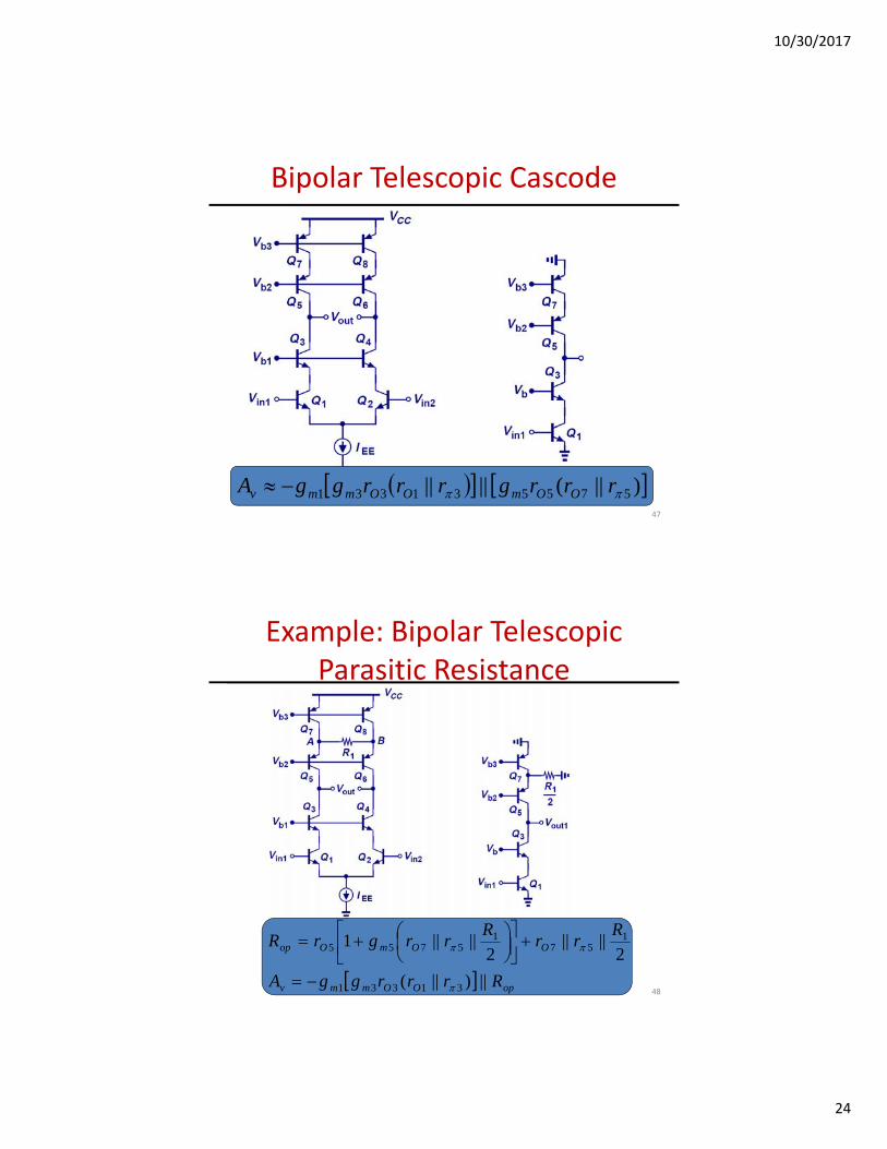
Bipolar Telescopic Cascode
47
)||(|||| 575531331 rrrgrrrggA OOmOOmmv
Example: Bipolar Telescopic Parasitic Resistance
48 opOOmmv
OOmOop
RrrrggA
Rrr
RrrgrR
||)||(
2||||
2||||1
31331
157
15755
10/30/2017
25
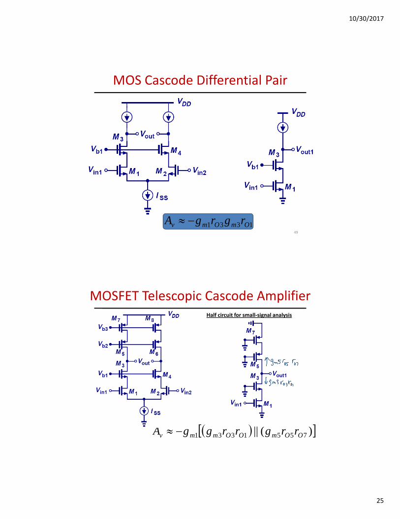
MOS Cascode Differential Pair
49
1331 OmOmv rgrgA
MOSFET Telescopic Cascode AmplifierHalf circuit for small‐signal analysis
)(|| 7551331 OOmOOmmv rrgrrggA
10/30/2017
26
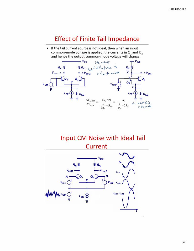
Effect of Finite Tail Impedance• If the tail current source is not ideal, then when an input
common‐mode voltage is applied, the currents in Q1 and Q2
and hence the output common‐mode voltage will change.
EEm
C
EEm
C
CMin
CMout
Rg
R
Rg
R
V
V
21
21
2/
,
,
Input CM Noise with Ideal Tail Current
52
10/30/2017
27
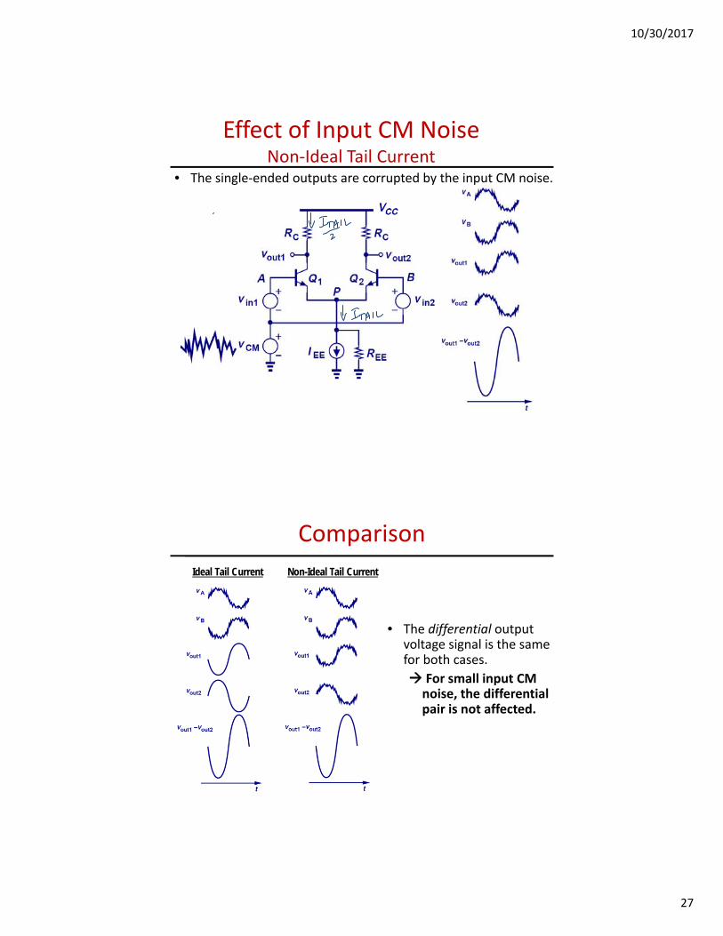
Effect of Input CM NoiseNon‐Ideal Tail Current
• The single‐ended outputs are corrupted by the input CM noise.
Comparison
Ideal Tail Current Non-Ideal Tail Current
• The differential output voltage signal is the same for both cases.
For small input CM noise, the differential pair is not affected.p

10/30/2017
28
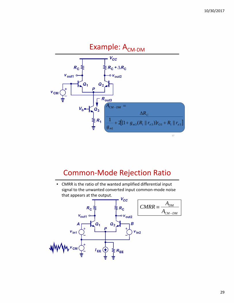
CM to DM Conversion Gain, ACM‐DM
• If finite tail impedance and asymmetry (e.g. in load resistance) are both present, then the differential output signal willcontain a portion of the input common‐mode signal.
EEm
CMC
EECm
CEECBECM
Rg
VI
RIg
IRIVV
21
22
1 CCout RIV
EEm
C
CM
out
Rg
R
V
V
2/1
21
2
CCoutoutout
CCCout
RIVVV
RRIV
CM to DM Conversion Gain, ACM‐DM
• If finite tail impedance and asymmetry are both present, then the differential output signal will contain a portion of the input common‐mode signal.contain a portion of the input common mode signal.
SSm
CMD
SSDm
DSSDGSCM
Rg
VI
RIg
IRIVV
21
22
2
1
DDDout
DDout
RRIV
RIV
21
2
DDoutoutout
DDDout
RIVVV
SSm
D
CM
out
Rg
R
V
V
2/1
10/30/2017
29
Example: ACM‐DM
A
57
3133131
||)]||(1[21
rRrrRgg
R
A
Omm
C
DMCM
• CMRR is the ratio of the wanted amplified differential input signal to the unwanted converted input common‐mode noise that appears at the output.
Common‐Mode Rejection Ratio
pp p
DMCM
DM
A
ACMRR
10/30/2017
30
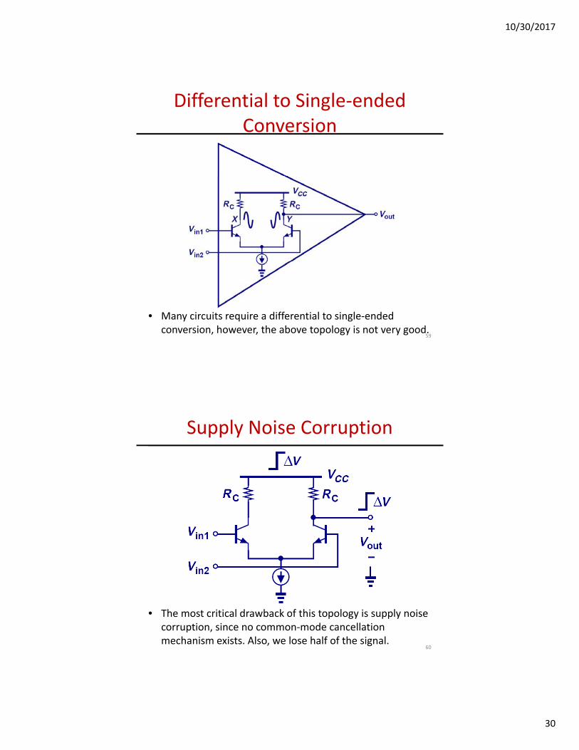
Differential to Single‐ended Conversion
59
• Many circuits require a differential to single‐ended conversion, however, the above topology is not very good.
Supply Noise Corruption
60
• The most critical drawback of this topology is supply noise corruption, since no common‐mode cancellation mechanism exists. Also, we lose half of the signal.
10/30/2017
31
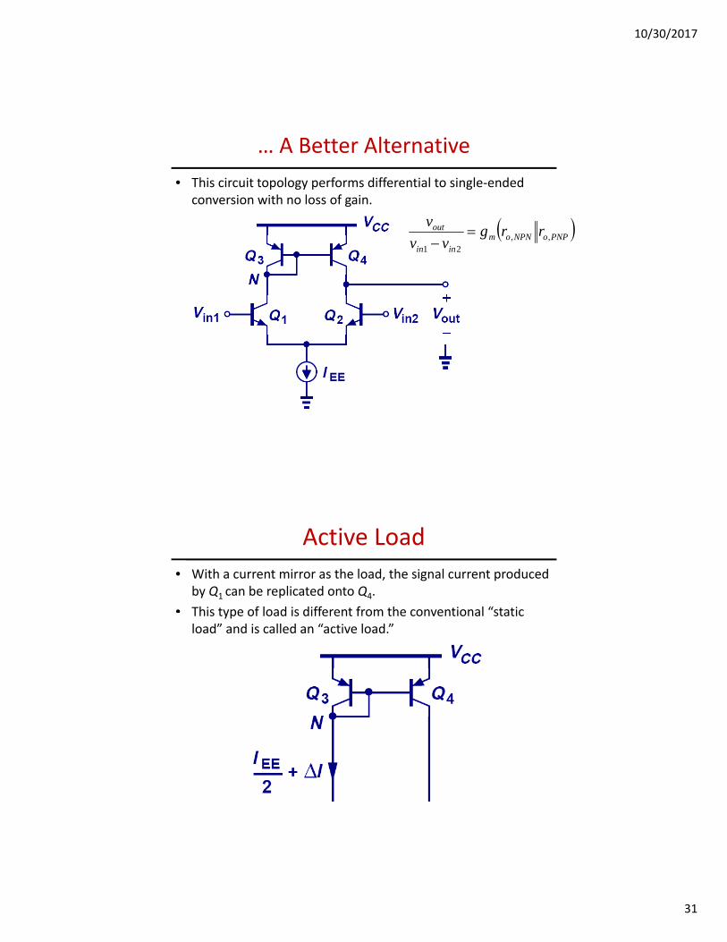
… A Better Alternative
• This circuit topology performs differential to single‐ended conversion with no loss of gain.
v
,,21
PNPoNPNominin
out rrgvv
v
Active Load
• With a current mirror as the load, the signal current produced by Q1 can be replicated onto Q4.
• This type of load is different from the conventional “staticThis type of load is different from the conventional static load” and is called an “active load.”
10/30/2017
32
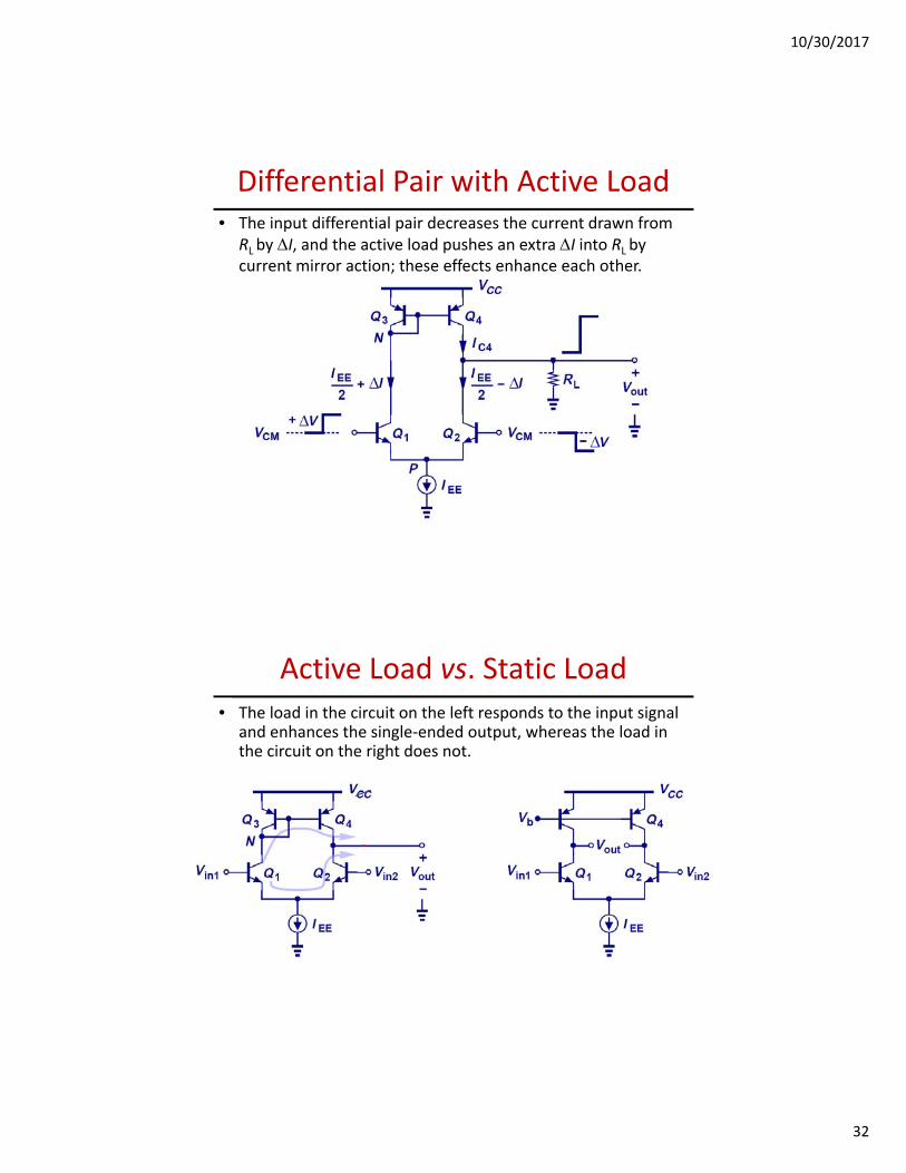
Differential Pair with Active Load• The input differential pair decreases the current drawn from
RL by I, and the active load pushes an extra I into RL by current mirror action; these effects enhance each other.
Active Load vs. Static Load• The load in the circuit on the left responds to the input signal
and enhances the single‐ended output, whereas the load in the circuit on the right does not.
10/30/2017
33
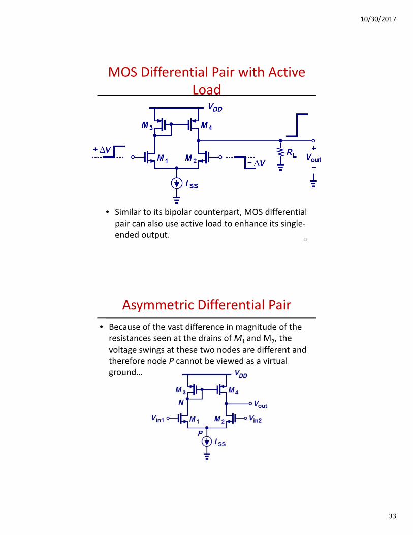
MOS Differential Pair with Active Load
65
• Similar to its bipolar counterpart, MOS differential pair can also use active load to enhance its single‐ended output.
Asymmetric Differential Pair
• Because of the vast difference in magnitude of the resistances seen at the drains of M1 and M2, the voltage swings at these two nodes are different andvoltage swings at these two nodes are different and therefore node P cannot be viewed as a virtual ground…
10/30/2017
34
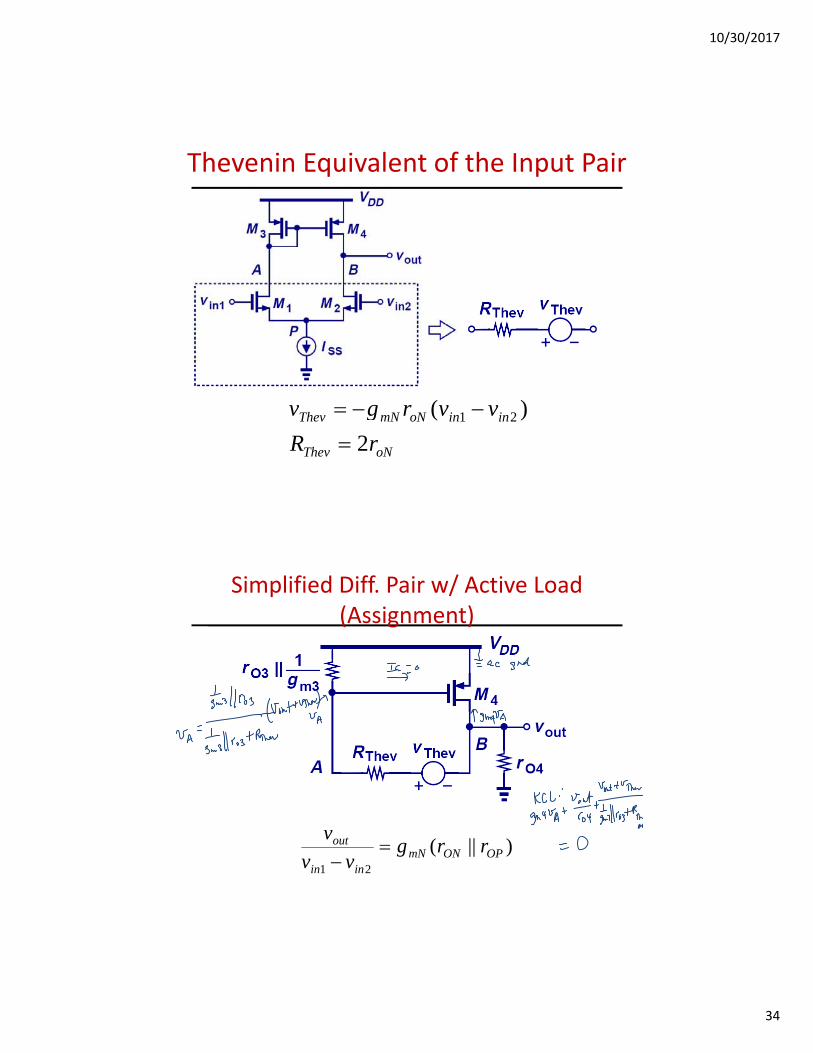
Thevenin Equivalent of the Input Pair
oNThev
ininoNmNThev
rR
vvrgv
2
)( 21
Simplified Diff. Pair w/ Active Load (Assignment)
)||(21
OPONmNinin
out rrgvv
v
10/30/2017
35
Next
• OPAMP
• Frequency response