atomistic simulations of stress concentration and
TRANSCRIPT

Progress in NUCLEAR SCIENCE and TECHNOLOGY, Vol. 2, pp.20-23 (2011)
c© 2011 Atomic Energy Society of Japan, All Rights Reserved.
20
ARTICLE
Atomistic Simulations of Stress Concentration and Dislocation Nucleation at Grain Boundaries
Tomohito TSURU 1,*, Yoshiyuki KAJI 1, Takashi TSUKADA 1 and Yoji SHIBUTANI 2
1 Japan Atomic Energy Agency, 2-4 Shirakata, Tokai-mura, Naka-gun, Ibaraki-ken, 319-1195, Japan
2 Osaka University, 2-1 Yamadaoka, Suita, Osaka, 565-0871, Japan
Dislocation channeling observed in irradiated metals has been thought to be one of the key stress factors in irradi-
ation assisted stress corrosion cracking since it is an evidence to suggest that the slip deformation is localized and that the strong misfit are generated at grain boundaries. In the present study, the stress concentration and defect nucleation of polycrystalline copper thin film is investigated by parallel molecular statics simulations. Uniaxial tensile deforma-tion is applied to the two-dimensional polycrystalline model. As a result, it is found that the stress concentration is observed at triple point of grain junctions in the elastic and initial stage of plastic deformation. Then partial disloca-tions are first generated from the small angle grain boundaries. Twin deformations occur at triple points and grain boundaries which result in both another site of stress concentration around grain boundaries and local displacement relevant to the Burgers vector at grain boundary. One distinguishing characteristic of deformation mode of polycrys-tal is that the stress distribution strongly correlated with the presence of the partial dislocations and twin boundaries. Stress relaxation within each grain is preferentially brought about by the dislocation nucleation and twin deformation.
KEYWORDS: polycrystalline copper thin film, grain boundary, molecular statics, stress concentration, twin deformation
I. Introduction1
Irradiation assisted stress corrosion cracking (IASCC) is the urgent issue of the ageing management and maintenance in boiling water reactors.1-3) A large amount of experimental studies of IASCC have been so far reported. Recently, the dislocation channeling which is the unique deformation mode in irradiated materials is observed and that thought to be one of the dominant stress factors in IASCC.4) In this sit-uation, glide dislocations interact with the grain boundaries which results in the stress concentration localized around grain boundary, and it is also worth considering that the lo-cal defect structures and local stress component change un-der deformation.
Grain boundary‒dislocation process has been thought to be one of the most important factors in the crystalline mate-rials which contribute significantly to plastic behavior as well as the dislocation‒dislocation process. Though these two lattice defects have been efficiently introduced in ma-terial strengthening well-known as Hall-Petch relation-ship,5,6) they have the negative effects in the fracture behavior due to the stress concentration and segregation site at the boundary. Dislocations are successively piled up be-side the grain boundary planes and they produce stress con-centration which causes the secondary defect nucleation and cracking. Piled-up dislocations at grain boundaries, as well as the disappearance of dislocations from the interaction between the dislocations and the grain boundaries under in-dentation-induced stress, have been observed recently by in
*Corresponding author, E-mail: [email protected]
situ nanoindentation with transmission electron microsco-py.7)
Atomistic simulations have been used in a large number of studies of grain boundaries and dislocations. The equili-brium structures and corresponding fundamental grain boundary fault energies of various kinds of coincidence site lattice (CSL) grain boundaries were investigated.8) In focus-ing on the specific type of the CSL, the dislocation dissocia-tion has been investigated by molecular dynamics simulation.9-11) The fundamental mechanisms of the interac-tion process between defect structures and individual crystal grain were comprehensively examined and showed the dis-sociation of the Burgers vector of glide dislocation in the interaction process. MD simulations have also been per-formed to capture the nanoscale plastic deformation of poly-crystalline materials.12-14)
Focusing on the specific grain boundaries in our previous study, density functional theory calculations have been ap-plied to evaluate the fault energies of the twin and several CSL grain boundaries, and molecular statics (MS) simula-tions are performed incipient plastic event on the twin and CSL grain boundaries.15) In the present study, we con-structed two-dimensional thin film model and investigated the deformation characteristics of polycrystalline metal using MS simulations. The incipient yield event and local stress distribution under tensile deformation were discussed.
II. Methods
1. Atomic Model We constructed a two-dimensional polycrystalline copper

Atomistic Simulations of Stress Concentration and Dislocation Nucleation at Grain Boundaries 21
VOL. 2, OCTOBER 2011
using Voronoi polyhedra division. At first, the central points of Voronoi polyhedra were randomly scattered, where the minimum value of a distance between the points was cor-responding to the diameters of the grains. In the present study, grain size was set to 20 nm. Then each grain region was determined by dividing between the scatted points. The single crystal oriented along the [110] , [111] and [112] directions was prepared and embedded in the polyhedral region. Each crystal was rotated in the [112] axis at an arbitrary angle, where slip deformation is restricted to a sin-gle slip system, that is dislocations are activated on the same system in the plastic deformation of each grain. Atoms overlapping around the boundary are removed and the min-imum distance between atoms is 70 percent of the nearest neighbor distance of perfect crystal. The atomic model of polycrystalline thin film is shown in Fig. 1. Here it has di-mensions of 150 × 150 × 1.33 nm3 including thirty-seven grains. A stable configuration was obtained by finite tem-perature molecular dynamics and molecular statics with conjugate gradient (CG) energy minimization. Here, a paral-lel computing technique was employed in the present calcu-lation.
2. Analysis Method
The fully-relaxed configuration of polycrystalline model was obtained by the CG method when the energy norm of all the atoms converged at 0.02 eV/Å, where the periodic boundary conditions were applied to all direction. The em-bedded atom method (EAM) type interatomic potential pro-posed by Mishin et al.16) was employed. The validity of the fault energies and confirmations of specific grain boundaries evaluated using empirical potential has been investigated by comparing DFT calculations and it has been confirmed that the fundamental properties of grain boundaries in copper were reproduced correctly.15)
Deformation analysis was performed by applying small increment of tensile strain in x direction, that is equal to 0.2% as shown in Fig. 1. Tensile stress xx can be evaluated
after fully-relaxed configuration, where all stress compo-nents except for thickness direction were converged by con-trolling cell matrix. Similar analysis was performed for the single crystal with the same size which has dimensions of [110] , [111] and [112] . Atomic stresses of all atoms
based on the Virial theorem were calculated in order to eva-luate the local stress condition. The formulation of atomic stress in using EAM potential is expressed by following eq-uation:
1,
1 1( ) ( ) ( ) ,
2
NI J
IJ
r rr F r
r
(1)
where is the volume of atom and r is the distance between atom and atom . The functions , F and are the conventional forms of EAM potential corresponding to the pair potential term, the embedded function and the elec-tron density function, respectively. The stress component of the whole system which is defined as the differentiation of the stored energy is obtained by averaging the atomic stress of all atoms as follows:
1
1 1,
Ntot
IJ IJIJ
E
V N
(2)
where V is the volume of the simulation box and N is the total number of atoms. Thus, the local stress in the vicinity of grain boundary and the stress of the system was evaluated efficiently. III. Results and Discussion
The relationships between tensile stress and strain of poly-crystalline and single crystalline thin film are shown in Fig. 2. The yield stresses were found to be 4.09 and 12.3 GPa in polycrystal and single crystal, respectively. It is noted that higher tensile strength of single crystal is achieved only in the case that preexisting dislocation does not exist in the model. It is found that the presence of grain boundaries
x
y
a
a
A
B
Fig. 1 Atomic model of polycrystalline copper thin film. Un-iaxial tensile strain is applied along the x direction.
0 0.05 0.1 0.150
5
10
15
Strain
Ten
sile
str
ess
(GPa
)
Single crystalPolycrystal ( d = 20 nm)
Fig. 2 Relationship between tensile stress and strain of single crystal and polycrystalline copper
22 Tomohito TSURU et al.
PROGRESS IN NUCLEAR SCIENCE AND TECHNOLOGY
lead to a significant decrease in yield stress since the grain boundaries act as the sources of initial yield process such as dislocation nucleation. On the other hand, the amount of decrease in tensile stress after the yield point is smaller than that of single crystal.
In elastic deformation region of polycrystal, stress is con-centrated at the grain boundary triple junction. Focusing on the specific area A of Fig. 1, the distribution of Von Mises equivalent stress is shown in Fig. 3, where atomic configura-tion at = 0.02 is depicted. It is confirmed that stress con-centrations occur at several triple junctions enclosed by a white dash line. Therefore the triple junction would be an origin of the stress concentration which results in the ear-ly-stage yield event.
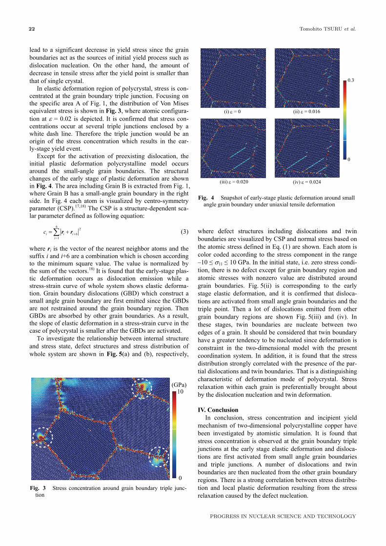
Except for the activation of preexisting dislocation, the initial plastic deformation polycrystalline model occurs around the small-angle grain boundaries. The structural changes of the early stage of plastic deformation are shown in Fig. 4. The area including Grain B is extracted from Fig. 1, where Grain B has a small-angle grain boundary in the right side. In Fig. 4 each atom is visualized by centro-symmetry parameter (CSP).17,18) The CSP is a structure-dependent sca-lar parameter defined as following equation:
62
61
i i ii
c
r r (3)
where ri is the vector of the nearest neighbor atoms and the suffix i and i+6 are a combination which is chosen according to the minimum square value. The value is normalized by the sum of the vectors.18) It is found that the early-stage plas-tic deformation occurs as dislocation emission while a stress-strain curve of whole system shows elastic deforma-tion. Grain boundary dislocations (GBD) which construct a small angle grain boundary are first emitted since the GBDs are not restrained around the grain boundary region. Then GBDs are absorbed by other grain boundaries. As a result, the slope of elastic deformation in a stress-strain curve in the case of polycrystal is smaller after the GBDs are activated.
To investigate the relationship between internal structure and stress state, defect structures and stress distribution of whole system are shown in Fig. 5(a) and (b), respectively,
where defect structures including dislocations and twin boundaries are visualized by CSP and normal stress based on the atomic stress defined in Eq. (1) are shown. Each atom is color coded according to the stress component in the range ‒10 ≤ 11 ≤ 10 GPa. In the initial state, i.e. zero stress condi-tion, there is no defect except for grain boundary region and atomic stresses with nonzero value are distributed around grain boundaries. Fig. 5(ii) is corresponding to the early stage elastic deformation, and it is confirmed that disloca-tions are activated from small angle grain boundaries and the triple point. Then a lot of dislocations emitted from other grain boundary regions are shown Fig. 5(iii) and (iv). In these stages, twin boundaries are nucleate between two edges of a grain. It should be considered that twin boundary have a greater tendency to be nucleated since deformation is constraint in the two-dimensional model with the present coordination system. In addition, it is found that the stress distribution strongly correlated with the presence of the par-tial dislocations and twin boundaries. That is a distinguishing characteristic of deformation mode of polycrystal. Stress relaxation within each grain is preferentially brought about by the dislocation nucleation and twin deformation. IV. Conclusion
In conclusion, stress concentration and incipient yield mechanism of two-dimensional polycrystalline copper have been investigated by atomistic simulation. It is found that stress concentration is observed at the grain boundary triple junctions at the early stage elastic deformation and disloca-tions are first activated from small angle grain boundaries and triple junctions. A number of dislocations and twin boundaries are then nucleated from the other grain boundary regions. There is a strong correlation between stress distribu-tion and local plastic deformation resulting from the stress relaxation caused by the defect nucleation.
0
10(GPa)
Fig. 3 Stress concentration around grain boundary triple junc-tion
(i) = 0 (ii) = 0.016
(iii) = 0.020 (iv) = 0.024
0
0.3
Fig. 4 Snapshot of early-stage plastic deformation around small angle grain boundary under uniaxial tensile deformation

Atomistic Simulations of Stress Concentration and Dislocation Nucleation at Grain Boundaries 23
VOL. 2, OCTOBER 2011
Acknowledgment
The authors T.T. and Y.S. acknowledge recurring finan-cial support from the Japan Society for the Promotion of Science (JSPS), Grant-in-Aid for Young Scientists (B, Grant No. 21760090)(T.T.) and Grants-in-Aid for Scientific Re-s �earch (S, Grant No. 20226004)(Y.S.). Technical support for parallel computing from the Center for Computational Science and e-Systems at the Japan Atomic Energy Agency is appreciated.
References
1) H. M. Chung, W. E. Ruther, J. E. Sanecki et al., “Irradia-tion-assisted stress corrosion cracking of austenitic stainless steels: recent progress and new approaches,” J. Nucl. Mater., 239[1], 61-79 (1996).
2) H. M. Chung, W. J. Shack, Irradiation-Assisted Stress Corro-sion Cracking Behavior of Austenitic Stainless Steels Applica-ble to LWR Core Internals, Energy Technology Division Argonne National Laboratory, Washington, DC (2006).
3) T. Tsukada, “Irradiation Assisted Stress Corrosion Cracking (IASCC),” Corr. Eng., 52[2], 66-72 (2003).
4) Z. Jiao, G. S. Was, “Localized deformation and IASCC initia-tion in austenitic stainless steels,” J. Nucl. Mater., 382[2-3], 203-209 (2008).
5) E. O. Hall, “The deformation and ageing of mild steel: III discussion of results,” Proc. Phys. Soc. London, B64, 747-753 (1951).
6) N. J. Petch, “The Cleavage strength of polycrystals,” J. Iron Steel Inst., 174, 25-28 (1953).
7) A. M. Minor, S. A. S. Asif, Z. W. Shan et al., “A new view of the onset of plasticity during the nanoindentation of alumi-num,” Nature. Mat., 5, 697-702 (2006).
8) J. D. Rittner, D. N. Seidman, “<110> symmetric tilt grain-boundary structures in fcc metals with low stack-ing-fault energies,” Phys. Rev., B54[10], 6999-7015 (1996).
9) B. J. Pestman, J. Th. M. de Hosson, V. Vitek et al., “Interac-tion between lattice dislocations and grain boundaries in F.C.C. materials,” Scripta Metall., 23[8], 1431-1436 (1989).
10) K. J. Kim, J. H. Yoon, M. H. Cho et al., “Molecular dynamics simulation of dislocation behavior during nanoindentation on a bicrystal with a 5 (210) grain boundary,” Mater. Lett., 60[28], 3367-3372 (2006).
11) Z. Jin, P. Gumbsch, K. Albe et al., “Interactions between non-screw lattice dislocations and coherent twin boundaries in face-centered cubic metals,” Acta Mater., 56[5], 1126-1135 (2008).
12) V. Yamakov, D. Wolf, M. Salazar, “Length-scale effects in the nucleation of extended dislocations in nanocrystalline Al by molecular-dynamics simulation,” Acta Mater., 49[14], 2713-2722 (2001).
13) V. Yamakov, D. Wolf, S. R. Phillpot et al., “Dislocation processes in the deformation of nanocrystalline aluminium by molecular-dynamics simulation,” Nature Mat., 1, 45-49 (2002).
14) H. Van Swygenhoven, P. M. Derlet, A. G. Frøseth, “Stacking fault energies and slip in nanocrystalline metals,” Nature Mat., 3, 399-403 (2004).
15) T. Tsuru, Y. Kaji, D. Matsunaka et al., “Incipient plasticity of twin and stable/unstable grain boundaries during nanoindenta-tion in copper,” Phys. Rev., B82[2], 024101 (2010).
16) Y. Mishin, D. Farkas, M. J. Mehl et al., “Structural stability and lattice defects in copper: Ab initio, tight-binding, and embedded-atom calculations,” Phys. Rev., B63[22], 224106 (2001).
17) C. L. Kelchner, S. J. Plimpton, J. C. Hamilton, “Dislocation nucleation and defect structure during surface indentation”, Phys. Rev., B58[17], 11085-11088 (1998).
18) J. Li, “AtomEye: an efficient atomistic configuration viewer,” Modelling Simul. Mater. Sci. Eng., 11[2], 173-177 (2003).
(a) CSP (b) Normal stress
(i) = 0
(ii) = 0.02
(iii) = 0.04
(iv) = 0.05
-10 10 (GPa)
0 0.3
Normal stress
CSP
Fig. 5 Internal structures and stress state of deformed polycrys-tal visualized by (a) CSP parameter and (b) normal stress in the tensile direction