asynchronous serial interface tpu function (uart)
TRANSCRIPT

Order this document by TPUPN07/D Rev. 1
APPLICATION NOTE
F
ree
sca
le S
em
ico
nd
uc
tor,
I
nc
...
Asynchronous Serial Interface TPU Function (UART)By Josef Fuchs and Charles Melear
1 Functional OverviewThe UART function uses two TPU channels to provide a 3-wire (RxD, TxD and GND) asynchronousserial interface. All standard baud rates and parity checking can be selected. The CPU interface toUART consists of a command register, which defines the operation (number of data bits, baud rate, par-ity); a status register, which gives information about the data register (empty or full) and errors (framingand parity); and a data register, which holds the data to be transmitted or data that has been received.These registers are implemented for the UART function using the TPU parameter RAM and host se-quence bits.
2 Detailed DescriptionThe UART consists of a transmitter, which can transmit serial data via a transmit data (TxD) pin, and areceiver, which can receive serial data via a receive data (RxD) pin. Both transmitter and receiver con-tain a single shift register that performs parallel-to-serial and serial-to-parallel conversion. Although aUART chip normally contains both the transmitter and receiver, implementing a full-duplex UART withthe TPU requires independent receiver and transmitter channels, because each TPU channel controlsonly one pin (a channel can be either a transmitter or a receiver, but not both at the same time). Whileat least two TPU channels must be used for a fully-functional UART, it is not necessary to use both sub-functions together, nor to use the same number of receivers and transmitters. For example, the TPUcould handle 13 transmitters and 3 receivers. There is also no restriction on which channels must beused to receive and transmit — any channel can be used to transmit data and any other channel canbe used to receive data. Since baud rate for each channel is specified independently, a transmitter canhave a different rate than a receiver.
The UART protocol allows selection of a parity bit to detect simple transmission errors. Parity can begenerated and checked in three different ways: odd, even and no parity. All parity-types are supportedwith the UART function.
The UART protocol is not fixed to a specific number of bits for one data word. Although 8-bit words arenormally used, some applications use 7-bit or 9-bit words. The UART function can use word lengthsfrom one to 14 bits. Maximum data size is determined by the structure of the receive data register. Thereceive data register also has two error flags built into it (FE and PE, bits 14 and 15) to simplify consis-tent reads of both data and flags. The number of transmitter stop bits is fixed at one. The receiver canalso handle fractional stop bits correctly, but the transmitter cannot generate fractional stop bits.
The UART function is double buffered. Both transmitter and receiver contain a shift register as well asa data register. The host CPU can write new data to the transmit data register while data is being trans-mitted, and can read data from the receive data register while data is being received.
The UART function can do back-to-back transfers. If data is available in time, the transmitter does notgenerate an idle line signal, but transmits exactly one stop bit followed by the start bit for the next data.An idle line condition only occurs if the transmit data register is empty after transferring data. The lengthof a transmit idle line condition is always divisible by the MATCH_RATE parameter. The receiver canhandle any length of idle line.
For More Information On This Product,
Go to: www.freescale.com

Fre
esc
ale
Se
mic
on
du
cto
r, I
Freescale Semiconductor, Inc.n
c..
.
Every data word begins with one start bit, which is always a logic zero. Following the start bit, a specifiednumber of data bits are transmitted least significant bit first, then a parity bit is generated and transmittedif parity is enabled. The end of the data word is marked by one stop bit, which is always a logic one. Anidle line consists of successive stop bits, which means that the line is at logic level one while idle. Forexample the ASCII character “A” is always transmitted as %0100000101.
This note uses the term “bit time” to refer to the time required to transmit or receive one bit. Bit time isdetermined by baud rate, using the formula:
The receiver detects a data word by sensing the falling edge of the start bit. Since the UART functionalways treats the first falling edge after the initialization service request as a valid start bit, a receivermust be enabled only when the line is idle. A received bit is sampled only once, approximately halfwaythrough the bit time.
3 Function Code SizeTotal TPU function code size determines what combination of functions can fit into a given ROM or em-ulation memory microcode space. UART function code size is:
59 µ instructions + 16 entries (8 long words) = 67 long words
4 Function ParametersThis section provides detailed descriptions of function parameters stored in channel parameter RAM.Figure 1 shows TPU parameter RAM address mapping. Figure 2 shows the parameter RAM assign-ment used by the UART function. In the diagrams, Y = M111, where M is the value of the module map-ping bit (MM) in the system integration module configuration register (Y = $7 or $F).
Except for the transmitter TDRE status bit and the receiver PE and FE error flags, parameters have thesame meaning for both the receiver and transmitter sub functions. In general, every TPU parametermust be accessed as a 16-bit value. Do not access any parameter as a byte value. Refer to the TPUReference Manual (TPURM/AD) for more information.
Bit Time 1Baud Rate----------------------------=
TPU Programming Library2 TPUPN07/D
For More Information On This Product,
Go to: www.freescale.com

Fre
esc
ale
Se
mic
on
du
cto
r, I
Freescale Semiconductor, Inc.n
c..
.
— = Not Implemented (reads as $00)
Figure 1 TPU Channel Parameter RAM CPU Address Map
Channel Base Parameter Address
Number Address 0 1 2 3 4 5 6 7
0 $YFFF## 00 02 04 06 08 0A — —1 $YFFF## 10 12 14 16 18 1A — —2 $YFFF## 20 22 24 26 28 2A — —3 $YFFF## 30 32 34 36 38 3A — —4 $YFFF## 40 42 44 46 48 4A — —5 $YFFF## 50 52 54 56 58 5A — —6 $YFFF## 60 62 64 66 68 6A — —7 $YFFF## 70 72 74 76 78 7A — —8 $YFFF## 80 82 84 86 88 8A — —9 $YFFF## 90 92 94 96 98 9A — —10 $YFFF## A0 A2 A4 A6 A8 AA — —11 $YFFF## B0 B2 B4 B6 B8 BA — —12 $YFFF## C0 C2 C4 C6 C8 CA — —13 $YFFF## D0 D2 D4 D6 D8 DA — —14 $YFFF## E0 E2 E4 E6 E8 EA EC EE15 $YFFF## F0 F2 F4 F6 F8 FA FC FE
TPU Programming LibraryTPUPN07/D 3
For More Information On This Product,
Go to: www.freescale.com

Fre
esc
ale
Se
mic
on
du
cto
r, I
Freescale Semiconductor, Inc.n
c..
.
W = Channel Number
Figure 2 UART Function Parameter RAM Assignment
4.1 RECEIVE_DATA_REG and TRANSMIT_DATA_REG
RECEIVE_DATA_REG holds data that has been received. The parameter word also contains the parityerror (PE) flag and the framing error (FE) flag. Although the parameter RAM address ofRECEIVE_DATA_REG can be read or written by the CPU, RECEIVE_DATA_REG should be treatedas a read-only register. TRANSMIT_DATA_REG holds data that is to be sent. The parameter word alsocontains the transmit data register empty (TDRE) status bit.
4.2 TDRE
This bit is set by the TPU to indicate that TRANSMIT_DATA_REG is empty. The function checks TDREstatus every bit time while the transmitter is idle to determine whether there is new data to be transmittedin the register. TDRE must be cleared during or after each write — it is best to write each new value toTRANSMIT_DATA_REG with the MSB cleared. The state of the TDRE bit is duplicated in the channelinterrupt status register. Either the TDRE or the interrupt status bit can be used to determine whetherthe transmitter is ready for new data. The interrupt status bit is best used in a polling environment, be-cause using it reduces the likelihood of a RAM collision caused by the TPU and CPU attempting to readTRANSMIT_DATA_REG at the same time. If the interrupt status bit is used, clear it before each writeto the data register. In any case, make certain that the TDRE is cleared before new data is written.
15 14 13 12 11 10 9 8 7 6 5 4 3 2 1 0$YFFFW0 PARITY_TEMP$YFFFW2 MATCH_RATE$YFFFW4 TDRE TRANSMIT_DATA_REG$YFFFW6 DATA_SIZE$YFFFW8 ACTUAL_BIT_COUNT$YFFFWA SHIFT_REGISTER
15 14 13 12 11 10 9 8 7 6 5 4 3 2 1 0$YFFFW0 PARITY_TEMP$YFFFW2 MATCH_RATE$YFFFW4 PE FE RECEIVE_DATA_REG$YFFFW6 DATA_SIZE$YFFFW8 ACTUAL_BIT_COUNT$YFFFWA SHIFT_REGISTER
Parameter Write AccessWritten by CPUWritten by TPUWritten by CPU and TPUUnused parameters
TPU Programming Library4 TPUPN07/D
For More Information On This Product,
Go to: www.freescale.com
Fre
esc
ale
Se
mic
on
du
cto
r, I
Freescale Semiconductor, Inc.n
c..
.
4.3 PE and FE
These bits are set or cleared by the TPU after each data word is received. Although the parameter RAMaddress of the receive data register can be read or written by the CPU, do not change the state of thesebits during operation. When parity checking is enabled, PE is set if a parity error occurs during reception.It remains cleared otherwise. A framing error occurs when the function determines that a stop bit is lowinstead of high. FE is set when a framing error is detected. It remains cleared otherwise. Both the PEand FE bits are valid only while the erroneous data is in RECEIVE_DATA_REG.
4.4 Receive Data Indicator
The TPU sets the interrupt status bit in the interrupt status register after writing a data word into theRECEIVE_DATA_REG. The interrupt status bit must be cleared by the CPU immediately before or afterreading the data register. In order to assure proper operation of the receiver, the entire parameter word,including RECEIVE_DATA_REG, PE, and FE state should be read at the same time.
4.5 MATCH_RATE
This parameter specifies serial transmission baud rate. MATCH_RATE is defined as TCR1 incrementsper bit time. MATCH_RATE must be written before the function is started by the INIT host service re-quest. It can be calculated using the formula:
This is the same as system clock frequency + TCR1 prescaler rate ÷ baud rate. MATCH_RATE mustnot be changed after function initialization.
4.6 DATA_SIZE
This parameter specifies the number of bits to be sent out or received in one data word. The parametercommonly has a value of eight, because most serial protocols use 8-bit words.
4.7 PARITY_TEMP
This parameter is written by a counter that counts the high bits in a word. The least significant bit of theparameter is used to generate parity. The parameter is used only by the UART function — the CPUmust not change this parameter value while the function is running.
4.8 ACTUAL_BIT_COUNT
This parameter is written by a counter that counts bits shifted out of SHIFT_REGISTER. The parameteris used only by the UART function — the CPU must not change this parameter value while the functionis running.
4.9 SHIFT_REGISTER
This parameter is used to shift data in or out. For a transmitter, data stored in TRANSMIT_DATA_REGis copied into SHIFT_REGISTER when the TDRE bit is set, then shifted out onto the serial line. For areceiver, data is shifted into SHIFT_REGISTER from the serial line until a word is complete, then copiedinto RECEIVE_DATA_REG.
MATCH_RATE TCR1_ClockBaud Rate
----------------------------------=
TPU Programming LibraryTPUPN07/D 5
For More Information On This Product,
Go to: www.freescale.com

Fre
esc
ale
Se
mic
on
du
cto
r, I
Freescale Semiconductor, Inc.n
c..
.
5 Host Interface to FunctionThis section provides information concerning the TPU host interface to the function. Figure 3 is a TPUaddress map. TPU register diagrams follow the figure. In the diagrams, Y = M111, where M is the valueof the module mapping bit (MM) in the system integration module configuration register (Y = $7 or $F).
Figure 3 TPU Address Map
CFS[4:0] — Function Number (Assigned during microcode assembly)
Address 15 8 7 0
$YFFE00 TPU MODULE CONFIGURATION REGISTER (TPUMCR)$YFFE02 TEST CONFIGURATION REGISTER (TCR)$YFFE04 DEVELOPMENT SUPPORT CONTROL REGISTER (DSCR)$YFFE06 DEVELOPMENT SUPPORT STATUS REGISTER (DSSR)$YFFE08 TPU INTERRUPT CONFIGURATION REGISTER (TICR)$YFFE0A CHANNEL INTERRUPT ENABLE REGISTER (CIER)$YFFE0C CHANNEL FUNCTION SELECTION REGISTER 0 (CFSR0)$YFFE0E CHANNEL FUNCTION SELECTION REGISTER 1 (CFSR1)$YFFE10 CHANNEL FUNCTION SELECTION REGISTER 2 (CFSR2)$YFFE12 CHANNEL FUNCTION SELECTION REGISTER 3 (CFSR3)$YFFE14 HOST SEQUENCE REGISTER 0 (HSQR0)$YFFE16 HOST SEQUENCE REGISTER 1 (HSQR1)$YFFE18 HOST SERVICE REQUEST REGISTER 0 (HSRR0)$YFFE1A HOST SERVICE REQUEST REGISTER 1 (HSRR1)$YFFE1C CHANNEL PRIORITY REGISTER 0 (CPR0)$YFFE1E CHANNEL PRIORITY REGISTER 1 (CPR1)$YFFE20 CHANNEL INTERRUPT STATUS REGISTER (CISR)$YFFE22 LINK REGISTER (LR)$YFFE24 SERVICE GRANT LATCH REGISTER (SGLR)$YFFE26 DECODED CHANNEL NUMBER REGISTER (DCNR)
CIER — Channel Interrupt Enable Register $YFFE0A
15 14 13 12 11 10 9 8 7 6 5 4 3 2 1 0
CH 15 CH 14 CH 13 CH 12 CH 11 CH 10 CH 9 CH 8 CH 7 CH 6 CH 5 CH 4 CH 3 CH 2 CH 1 CH 0
CH Interrupt Enable
0 No interrupts 1 Interrupts enabled
CFSR[0:3] — Channel Function Select Registers $YFFE0C – $YFFE12
15 14 13 12 11 10 9 8 7 6 5 4 3 2 1 0
CFS (CH 15, 11, 7, 3) CFS (CH 14, 10, 6, 2) CFS (CH 13, 9, 5, 1) CFS (CH 12, 8, 4, 0)
TPU Programming Library6 TPUPN07/D
For More Information On This Product,
Go to: www.freescale.com

Fre
esc
ale
Se
mic
on
du
cto
r, I
Freescale Semiconductor, Inc.n
c..
.
HSQR[0:1] — Host Sequence Registers $YFFE14 – $YFFE16
15 14 13 12 11 10 9 8 7 6 5 4 3 2 1 0
CH 15, 7 CH 14, 6 CH 13, 5 CH 12, 4 CH 11, 3 CH 10, 2 CH 9, 1 CH 8, 0
CH Operating Mode
00 No Parity01 No Parity10 Even Parity11 Odd Parity
HSRR[1:0] — Host Service Request Registers $YFFE18 – $YFFE1A
15 14 13 12 11 10 9 8 7 6 5 4 3 2 1 0
CH 15, 7 CH 14, 6 CH 13, 5 CH 12, 4 CH 11, 3 CH 10, 2 CH 9, 1 CH 8, 0
CH Initialization
00 Not Used01 Not Used10 Transmit11 Receive
CPR[1:0] — Channel Priority Registers $YFFE1C – $YFFE1E
15 14 13 12 11 10 9 8 7 6 5 4 3 2 1 0
CH 15, 7 CH 14, 6 CH 13, 5 CH 12, 4 CH 11, 3 CH 10, 2 CH 9, 1 CH 8, 0
CH Channel Priority
00 Off01 Low10 Middle11 High
CISR — Channel Interrupt Status Register $YFFE20
15 14 13 12 11 10 9 8 7 6 5 4 3 2 1 0
CH 15 CH 14 CH 13 CH 12 CH 11 CH 10 CH 9 CH 8 CH 7 CH 6 CH 5 CH 4 CH 3 CH 2 CH 1 CH 0
CH Interrupt Status
0 No Interrupt1 Interrupt Request
TPU Programming LibraryTPUPN07/D 7
For More Information On This Product,
Go to: www.freescale.com

Fre
esc
ale
Se
mic
on
du
cto
r, I
Freescale Semiconductor, Inc.n
c..
.
6 Function Configuration
6.1 Transmitter InitializationSet parameters:
Write the desired baud rate value to MATCH_RATE. Write $8000 to TRANSMIT_DATA_REG, to set TDRE. TDRE is not initialized by the host servicerequest.Write the number of bits per data word to DATA_SIZE. This number represents only the number ofdata bits, and does not include start and stop bits or the parity bit.
Write the channel function select field. This value depends on the actual TPU code.Set the host sequence bits to select the desired parity.Clear any pending interrupt.Set interrupt enable if required.Issue host service request by writing %11 to the host service request field.Write channel priority to start the function.When initialization is complete, the interrupt status bit is set to indicate that TRANSMIT_DATA_REG isempty.
6.2 Transmitting DataWait for TDRE or interrupt status bit to be set, indicating that TRANSMIT_DATA_REG is empty.Clear the MSB of the data word.If using the interrupt status bit, clear it before writing TRANSMIT_DATA_REG.Write the data word to TRANSMIT_DATA_REG.
6.3 Receiver InitializationSet parameters:
Write the desired baud rate value to MATCH_RATE. Write the number of bits per data word to DATA_SIZE. This number represents only the number ofdata bits, and does not include start and stop bits or the parity bit.
Write the channel function select field. This value depends on the actual TPU code.Set the host sequence bits to select the desired parity.Clear any pending interrupt.Set interrupt enable if required.Issue host service request by writing%10 to the host service request field.Write channel priority to start the function.
6.4 Receiving DataWait for interrupt status bit to be set, indicating that RECEIVE_DATA_REG is full.Read RECEIVE_DATA_REG.Clear the interrupt status bit.Check PE and FE bit status, using value read from the parameter. Do not read the parameter again forerror testing.
7 Performance and Use of Function
7.1 Performance
Like all TPU functions, the performance limit of the UART function in a given application depends onthe service time (latency) of other active TPU channels. This is due to the operational nature of thescheduler. To calculate the maximum performance of the function the user must know the executiontime for the different states of the functions running at the same time. In general, the maximum servicelatency for every mode of the UART function must be less than one bit time, which depends on the baudrate. The function must be allowed this amount of time by the other running functions. For example, at9600 baud the maximum latency of the UART function must be less than 104 µs.
TPU Programming Library8 TPUPN07/D
For More Information On This Product,
Go to: www.freescale.com

Fre
esc
ale
Se
mic
on
du
cto
r, I
Freescale Semiconductor, Inc.n
c..
.
NOTE: Execution times do not include the time slot transition time (TST = 10 or 14 CPU clocks)
7.1.1 Latency Examples
All examples assume that only the UART function is running. Examples are for absolute worst case,e.g. all receivers receive a stop bit at the same time, since this is the longest state.
When only transmitters are running, maximum baud rate for all channels combined is 360 kbaud. Thiscan be one transmitter with 360 kbaud, or nine with 38.4 kbaud, or any other combination.
When only receivers are running, maximum baud rate is 233 kbaud. This can be one receiver with 233kbaud, or six with 38.4 kbaud, or any other combination.
When both receivers and transmitters are running, maximum baud rate is 142 kbaud. This can be onepair running at 142 kbaud, or three pair at 38.4 kbaud, or seven pair at 19.2 kbaud, or any other com-bination.
7.2 Differences from a Conventional UART
The UART function does not implement MODEM control signals like RTS, CTS, and CD.
The receiver does not provide an overrun bit that is set when a received data word is not read by theCPU before a new data word arrives.
The transmitter does not provide an underrun bit.
The status bits are not cleared automatically by reading or writing the data registers.
The number of stop bits is fixed to one.
Table 1 UART Function State Timing
State Number and Name Max. CPU Clock Cycles RAM Accesses by TPU
S1 Init_Receiver 4 0S2 Init_Transmitter 4 1S3 Polling_TDRE
(Transmitter only)TDRE = 1TDRE = 0
1622
7
S4 Sending_Data(Transmitter only)Transmit stop bit with parityTransmit stop bit, no parityTransmit parityTransmit one data bit
12203228
8
S5 Receiving_Start_Bit(Receiver only)No parity selectedParity selected
1618
2
S6 Receiving_Data_Bit(Receiver only)
Receive stop bitReceive one data bit
44 + (2 ∗ (16 – DATA_SIZE))20
8
TPU Programming LibraryTPUPN07/D 9
For More Information On This Product,
Go to: www.freescale.com

Fre
esc
ale
Se
mic
on
du
cto
r, I
Freescale Semiconductor, Inc.n
c..
.
7.3 Limitations
To minimize TPU loading, the receiver does single sampling only. Each bit is sampled only once in themiddle of the bit time — any glitch on the receive data line may cause erroneous data. The receiverdoes not detect idle line or break conditions, nor does the transmitter generate a break character.
Status bits must be handled by the CPU. These bits are set automatically by the TPU, but cannot becleared by the function. The bits must be cleared by the CPU. This may cause a problem when the in-terrupt status bit is used to indicate that data has been received.
The interrupt status bit must be cleared by the CPU immediately before and after a read. The problemarises if the UART function receives new data before both actions are complete.
If the status bit is cleared immediately before reading data, a new data word might arrive before the pre-vious data is read. In this case, the new word would be read, then the status bit would be set again,causing the word to be read a second time.
If the status bit is cleared immediately after data is read, a new data word might arrive before the statusbit is cleared. In this case, the new data is not read, because the interrupt status bit is not set again.
To avoid these problems, the read routine must respond to the interrupt status bit quickly. The routinemust execute completely before the function copies the received value from SHIFT_REGISTER toRECEIVE_DATA_REG. For a 9600 baud receiver, the time to receive an 8-bit data word without parityis about 1 ms. The read routine must respond to the interrupt status bit within this time.
8 Examples
8.1 Example A: Implementing a Receiver
8.1.1 Description
This example shows how to set up the UART function as a receiver, and how to service the incomingdata. The user must decide how to handle parity and framing errors.
8.1.2 Initialization
Sets up channel 0 as a receiver, with an 8-bit data word and no parity, using the variable BAUD to de-termine baud rate. BAUD value is a function of baud rate, IMB clock frequency, and TPU prescaler set-ting. The actual Baud rate is 9600. Received data is stored in RAM at addresses starting at $6000. Thevalue of the FUNCNUM variable is assigned during microcode assembly.
8.1.3 ListingFUNCNUM EQU $000B ;Function Number for UARTBAUD EQU $01B2 ;9600 Baud RateMATCH_RATE EQU $FFFF02 ;Parameter RAMRECEIVE_DATA EQU $FFFF04 ;Parameter RAMDATA_SIZE EQU $FFFF06 ;Parameter RAMTPUMCR EQU $FFFE00 ;TPU MODULE CONFIGURATION REGISTERTICR EQU $FFFE08 ;TPU INTERRUPT CONFIGURATION REGISTERCIER EQU $FFFE0A ;CHANNEL INTERRUPT ENABLE REGISTERCFSR3 EQU $FFFE12 ;CHANNEL FUNCTION SELECT REGISTER 3HSQR1 EQU $FFFE16 ;HOST SEQUENCE REGISTER 1HSRR1 EQU $FFFE1A ;HOST SERVICE REQUEST REGISTER 1CPR0 EQU $FFFE1C ;CHANNEL PRIORITY REGISTER 0CPR1 EQU $FFFE1E ;CHANNEL PRIORITY REGISTER 1CISR EQU $FFFE20 ;CHANNEL INTERRUPT STATUS REGISTER
ORG $0 ;Initialize the Reset Vectors
TPU Programming Library10 TPUPN07/D
For More Information On This Product,
Go to: www.freescale.com

Fre
esc
ale
Se
mic
on
du
cto
r, I
Freescale Semiconductor, Inc.n
c..
.
DW $0000 ;Set Stack Pointer at 3FFCDW $3FFCDW $0000 ;Set IP at $3000DW $3000
INCLUDE 'ORG00008.ASM'* This file initializes the interrupt and exception* vectors ($00008 - $001FF). If an unplanned* interrupt occurs, program flow will continue at* the label “BDM” which must exist in the user's* main program. This label should have a “BGND”* instruction to return control back to the monitor.
ORG $3000 ;Start Program at $3000INITSYS:
ORI.W #$2700,SR ;ensure supervisor mode, interrupts maskedMOVE.L #$00000,D0MOVEC D0,VBR ;place VBR at $00000MOVEA.L#$FFF000,A0 ;set A0 to point to start of SIM registersMOVE.W D0,($A20,A0) ;turn COP (software watchdog) offMOVEQ #$7F,D0 ;w=0, x=1, y=111111MOVE.B D0,($A04,A0) ;system clock = 16.78MHzLEA.L $3FFC,A7 ;Initialize Stack Pointer at $3FFCLEA $6000,A0 ;Initialize A0 to Address $6000
***** Initialize TPU Register and Parameter RAM *****INITIALIZE:
CLR.L (CPR0).L ;Ensure Priority Bits are Cleared to 0MOVE.L #INT_SERVICE,($0100).L ;Address of Interrupt RoutineMOVE.W #$04CF,(TPUMCR).L ;TCR1 = Divide by 1, Int ARB ID = $F
;Prescaler Clock = Divide by 4MOVE.W #$0540,(TICR).L ;Interrupt Level = 5, Vector Number = $40MOVE.W #BAUD,(MATCH_RATE).L ;Set 9600 Baud RateMOVE.W #$0000,(RECEIVE_DATA).L ;Clear Receiver and Receive FlagsMOVE.W #$0008,(DATA_SIZE).L ;Set Data SizeANDI.W #$FFFE,(CISR).L ;Clear Channel 0 Interrupt FlagsMOVE.W #$0001,(CIER).L ;Enable Channel 0 InterruptsMOVE.W #FUNCNUM,(CFSR3).L ;Set Channel 0 to UART functionMOVE.W #$0000,(HSQR1).L ;Select No ParityMOVE.W #$0002,(HSRR1).L ;Host Service Request Code for ReceiveMOVE.W #$0003,(CPR1).L ;Select High PriorityANDI.W #$F0FF,SR ;Set Interrupt Priority Mask Level to 0
***** Main Program *****MAIN:
BRA MAIN ;branch back to main
***** Interrupts/Exceptions *****INT_SERVICE:
ANDI.W #$FFFE,(CISR).L ;Clear Channel 0 Interrupt FlagsMOVE.W (RECEIVE_DATA).L,D0 ;Move Received Data to D0ANDI.W #$00FF,D0 ;Data Register 0 has Received ByteMOVE.B D0,(A0)+RTE
BDM: BGND ;exception vectors point here
;and put the user in background debug mode
TPU Programming LibraryTPUPN07/D 11
For More Information On This Product,
Go to: www.freescale.com

Fre
esc
ale
Se
mic
on
du
cto
r, I
Freescale Semiconductor, Inc.n
c..
.
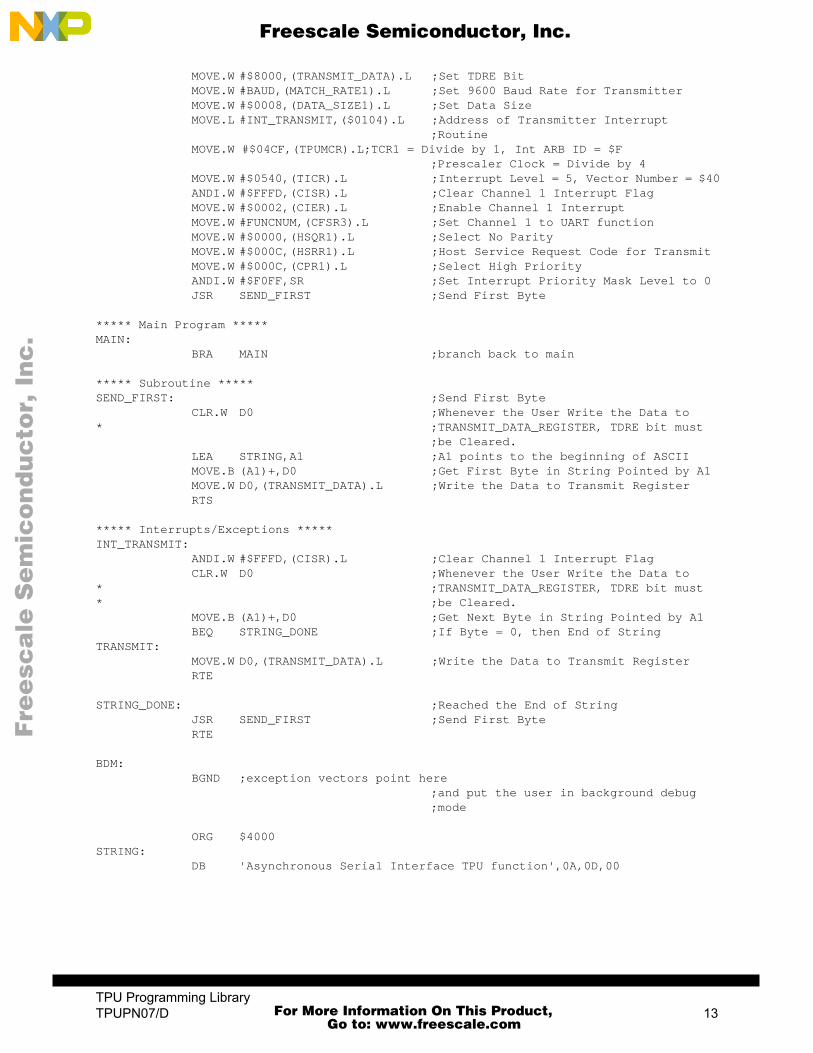
8.2 Example B: Implementing a Transmitter
8.2.1 Description
This example shows how to set up the UART function as a transmitter, and how to service the transmitbuffer.
8.2.2 Initialization
Sets up channel 1 as a transmitter, with an 8-bit data word and no parity, using the variable BAUD todetermine baud rate. BAUD value is a function of baud rate, IMB clock frequency, and TPU prescalersetting. The actual Baud rate is 9600 using 4.1 MHz TCR1_Clock. The value of the FUNCNUM variableis assigned during microcode assembly.
8.2.3 ListingFUNCNUM EQU $00B0 ;Function Number for UARTBAUD EQU $01B2 ;9600 Baud RateMATCH_RATE1 EQU $FFFF12 ;Parameter RAMTRANSMIT_DATA EQU $FFFF14 ;Parameter RAMDATA_SIZE1 EQU $FFFF16 ;Parameter RAMTPUMCR EQU $FFFE00 ;TPU MODULE CONFIGURATION REGISTERTICR EQU $FFFE08 ;TPU INTERRUPT CONFIGURATION REGISTERCIER EQU $FFFE0A ;CHANNEL INTERRUPT ENABLE REGISTERCFSR3 EQU $FFFE12 ;CHANNEL FUNCTION SELECT REGISTER 3HSQR1 EQU $FFFE16 ;HOST SEQUENCE REGISTER 1HSRR1 EQU $FFFE1A ;HOST SERVICE REQUEST REGISTER 1CPR0 EQU $FFFE1C ;CHANNEL PRIORITY REGISTER 0CPR1 EQU $FFFE1E ;CHANNEL PRIORITY REGISTER 1CISR EQU $FFFE20 ;CHANNEL INTERRUPT STATUS REGISTER
ORG $0 ;Initialize the Reset VectorsDW $0000 ;Set Stack Pointer at 3FFCDW $3FFCDW $0000 ;Set IP at $3000DW $3000
INCLUDE'ORG00008.ASM'* This file initializes the interrupt and exception* vectors ($00008 - $001FF). If an unplanned* interrupt occurs, program flow will continue at* the label “BDM” which must exist in the user's* main program. This label should have a “BGND”* instruction to return control back to the monitor.
ORG $3000 ;Start Program at $3000INITSYS:
ORI.W #$2700,SR ;ensure supervisor mode, interrupts maskedMOVE.L #$00000,D0MOVEC D0,VBR ;place VBR at $00000MOVEA.L#$FFF000,A0 ;set A0 to point to start of SIM registersMOVE.W D0,($A20,A0) ;turn COP (software watchdog) offMOVEQ #$7F,D0 ;w=0, x=1, y=111111MOVE.B D0,($A04,A0) ;system clock = 16.78MHzLEA.L $3FFC,A7 ;Initialize Stack Pointer at $3FFCLEA $6000,A0 ;Initialize A0 to Address $6000
***** Initialize TPU Register and Parameter RAM *****INITIALIZE:
CLR.L (CPR0).L ;Ensure Priority Bits are Cleared to 0
TPU Programming Library12 TPUPN07/D
For More Information On This Product,
Go to: www.freescale.com
Fre
esc
ale
Se
mic
on
du
cto
r, I
Freescale Semiconductor, Inc.n
c..
.
MOVE.W #$8000,(TRANSMIT_DATA).L ;Set TDRE BitMOVE.W #BAUD,(MATCH_RATE1).L ;Set 9600 Baud Rate for TransmitterMOVE.W #$0008,(DATA_SIZE1).L ;Set Data SizeMOVE.L #INT_TRANSMIT,($0104).L ;Address of Transmitter Interrupt
;RoutineMOVE.W #$04CF,(TPUMCR).L;TCR1 = Divide by 1, Int ARB ID = $F
;Prescaler Clock = Divide by 4MOVE.W #$0540,(TICR).L ;Interrupt Level = 5, Vector Number = $40ANDI.W #$FFFD,(CISR).L ;Clear Channel 1 Interrupt FlagMOVE.W #$0002,(CIER).L ;Enable Channel 1 InterruptMOVE.W #FUNCNUM,(CFSR3).L ;Set Channel 1 to UART functionMOVE.W #$0000,(HSQR1).L ;Select No ParityMOVE.W #$000C,(HSRR1).L ;Host Service Request Code for TransmitMOVE.W #$000C,(CPR1).L ;Select High PriorityANDI.W #$F0FF,SR ;Set Interrupt Priority Mask Level to 0JSR SEND_FIRST ;Send First Byte
***** Main Program *****MAIN:
BRA MAIN ;branch back to main
***** Subroutine *****SEND_FIRST: ;Send First Byte
CLR.W D0 ;Whenever the User Write the Data to * ;TRANSMIT_DATA_REGISTER, TDRE bit must
;be Cleared.LEA STRING,A1 ;A1 points to the beginning of ASCIIMOVE.B (A1)+,D0 ;Get First Byte in String Pointed by A1MOVE.W D0,(TRANSMIT_DATA).L ;Write the Data to Transmit RegisterRTS
***** Interrupts/Exceptions *****INT_TRANSMIT:
ANDI.W #$FFFD,(CISR).L ;Clear Channel 1 Interrupt FlagCLR.W D0 ;Whenever the User Write the Data to
* ;TRANSMIT_DATA_REGISTER, TDRE bit must* ;be Cleared.
MOVE.B (A1)+,D0 ;Get Next Byte in String Pointed by A1BEQ STRING_DONE ;If Byte = 0, then End of String
TRANSMIT:MOVE.W D0,(TRANSMIT_DATA).L ;Write the Data to Transmit RegisterRTE
STRING_DONE: ;Reached the End of StringJSR SEND_FIRST ;Send First Byte RTE
BDM:BGND ;exception vectors point here
;and put the user in background debug ;mode
ORG $4000STRING:
DB 'Asynchronous Serial Interface TPU function',0A,0D,00
TPU Programming LibraryTPUPN07/D 13
For More Information On This Product,
Go to: www.freescale.com

Fre
esc
ale
Se
mic
on
du
cto
r, I
Freescale Semiconductor, Inc.n
c..
.
9 Function AlgorithmThe following description is provided as a guide only, to aid understanding of the function. The exactsequence of operations in microcode may be different from that shown, in order to optimize speed andcode size. TPU microcode source listings for all functions in the TPU function library can be downloadedfrom the Freescale Freeware bulletin board. Refer to Using the TPU Function Library and TPU EmulationMode (TPUPN00/D) for detailed instructions on downloading and compiling microcode.
The UART function consists of six states, described below.
9.1 State 1: Init_Receiver
This state is entered as a result of a host service request type %10. It configures the channel for inputwith TCR1 as timebase and ‘detect falling edge’ pin control. The channel is configured to wait for thefalling edge of the start bit.
9.2 State 2: Init_Transmitter
This state is entered as a result of a host service request type %11. It configures the channel for outputwith TCR1 as timebase, sets the pin to high (idle state) and defines ‘no action’ pin control. It sets up amatch at (TCR1 + MATCH_RATE) which causes entry to state 3 (Polling_TDRE).
9.3 State 3: Polling_TDRE (Transmitter only)
This state is entered as a result of a match. It checks the TDRE bit. A new match is scheduled at (Eventtime + MATCH_RATE). If TDRE is not set, the ‘no action’ option is used, otherwise ‘pin_low’ is selectedto generate the start bit. In this case RECEIVE_DATA_REG is copied to the SHIFT_REGISTER andTDRE is set. An internal flag is set to enter state 4 instead of state 3 next time.
9.4 State 4: Sending_Data (Transmitter only)
This state is entered as a result of a match. A new match is scheduled at (Event time + MATCH_RATE).The pin action is defined by the next bit to be sent out. After sending the stop bit, the internal flag iscleared, to enter state 3 instead of state 4 next time.
9.5 State 5: Receiving_Start_Bit (Receiver only)
This state waits for the falling edge of a start bit. It is entered as a result of a falling edge transition. Amatch is scheduled at (Event time + MATCH_RATE * 1.5) to be able to get the middle of the first bit.Also an internal flag is set to enter state 6 instead of state 5 next time.
9.6 State 6: Receiving_Data_Bit (Receiver only)
This state is entered as a result of a match. The pin state is shifted into SHIFT_REGISTER. If this is notthe last bit, then a new match is scheduled at (Event time + MATCH_RATE), otherwise this bit (stop bit)is checked as well as the parity (if selected). The data is copied to RECEIVE_DATA_REG and an inter-rupt service request is made. The channel is again configured to wait for the next falling edge (next startbit). The internal flag is cleared again to enter state 5 instead of state 6 next time.
TPU Programming Library14 TPUPN07/D
For More Information On This Product,
Go to: www.freescale.com

Fre
esc
ale
Se
mic
on
du
cto
r, I
Freescale Semiconductor, Inc.n
c..
.
TPU Programming LibraryTPUPN07/D 15
For More Information On This Product,
Go to: www.freescale.com

Fre
esc
ale
Se
mic
on
du
cto
r, I
Freescale Semiconductor, Inc.n
c..
.
For More Information On This Product, Go to: www.freescale.com