asynchronous microengines for …niti/msthesis.pdfasynchronous microengines for network processing...
TRANSCRIPT

ASYNCHRONOUS MICROENGINES FOR NETWORK
PROCESSING
by
Niti Madan
A thesis submitted to the faculty ofThe University of Utah
in partial fulfillment of the requirements for the degree of
Master of Science
in
Computer Science
School of Computing
The University of Utah
May 2006

Copyright c© Niti Madan 2006
All Rights Reserved

THE UNIVERSITY OF UTAH GRADUATE SCHOOL
SUPERVISORY COMMITTEE APPROVAL
of a thesis submitted by
Niti Madan
This thesis has been read by each member of the following supervisory committee and by majorityvote has been found to be satisfactory.
Chair: Erik Brunvand
Ganesh Gopalakrishnan
Al Davis

THE UNIVERSITY OF UTAH GRADUATE SCHOOL
FINAL READING APPROVAL
To the Graduate Council of the University of Utah:
I have read the thesis of Niti Madan in its final form and havefound that (1) its format, citations, and bibliographic style are consistent and acceptable; (2) itsillustrative materials including figures, tables, and charts are in place; and (3) the final manuscriptis satisfactory to the Supervisory Committee and is ready for submission to The Graduate School.
Date Erik BrunvandChair: Supervisory Committee
Approved for the Major Department
Christopher R. JohnsonChair/Director
Approved for the Graduate Council
David S. ChapmanDean of The Graduate School
ABSTRACT
We present a network processor architecture that is based on asynchronous microcoded
controller hardware (a.k.a asynchronous microengine). The focus of this work is not
on the processor architecture, but rather on the asynchronous microcoded style used to
build such an architecture. This circuit style tries to fill the performance gap between a
specialized ASIC (Application-Specific Integrated Circuit) and a more general network
processor implementation. It does this by providing a microcoded framework that is
close in performance to ASICs and is also programmable at the finer granularity of
microcode. Our approach exploits the inherent advantages of asynchronous design tech-
niques to exhibit modularity, average case completion time, lower power consumption
and low electromagnetic interference . We have evaluated our circuit style by demon-
strating fast-path IP (Internet Protocol) routing as the packet processing application. The
flexibility aspect of this design has been demonstrated by adding firewalling functionality
to the router by modifying the microcode. Each microengine core is specialized enough
for different packet processing kernels yet generic enough to handle newer protocols
and applications. For shorter design cycle time, we have implemented our design using
Xilinx SpartanII FPGA board. However, we are extrapolating our results for a best-guess
ASIC implementation.

To my parents

CONTENTS
ABSTRACT . . . . . . . . . . . . . . . . . . . . . . . . . . . . . . . . . . . . . . . . . . . . . . . . . . . iv
LIST OF FIGURES . . . . . . . . . . . . . . . . . . . . . . . . . . . . . . . . . . . . . . . . . . . . . viii
LIST OF TABLES . . . . . . . . . . . . . . . . . . . . . . . . . . . . . . . . . . . . . . . . . . . . . . x
ACKNOWLEDGMENTS . . . . . . . . . . . . . . . . . . . . . . . . . . . . . . . . . . . . . . . . xii
CHAPTERS
1. INTRODUCTION . . . . . . . . . . . . . . . . . . . . . . . . . . . . . . . . . . . . . . . . . . 1
2. BACKGROUND . . . . . . . . . . . . . . . . . . . . . . . . . . . . . . . . . . . . . . . . . . . . 4
2.1 Asynchronous Design . . . . . . . . . . . . . . . . . . . . . . . . . . . . . . . . . . . . . . 42.2 Advantages of Asynchronous Design . . . . . . . . . . . . . . . . . . . . . . . . . . . 52.3 Asynchronous Microengine . . . . . . . . . . . . . . . . . . . . . . . . . . . . . . . . . . 6
2.3.1 Architecture Overview . . . . . . . . . . . . . . . . . . . . . . . . . . . . . . . . . 72.3.2 Microengine Execution . . . . . . . . . . . . . . . . . . . . . . . . . . . . . . . . . 82.3.3 Next Address Generation . . . . . . . . . . . . . . . . . . . . . . . . . . . . . . . 82.3.4 Microcode Fields . . . . . . . . . . . . . . . . . . . . . . . . . . . . . . . . . . . . . 92.3.5 Control Units . . . . . . . . . . . . . . . . . . . . . . . . . . . . . . . . . . . . . . . . 10
2.4 Internet Protocol(IP) . . . . . . . . . . . . . . . . . . . . . . . . . . . . . . . . . . . . . . . 122.4.1 IP Header . . . . . . . . . . . . . . . . . . . . . . . . . . . . . . . . . . . . . . . . . . . 132.4.2 IP Over Ethernet Layer . . . . . . . . . . . . . . . . . . . . . . . . . . . . . . . . . 152.4.3 IP Router . . . . . . . . . . . . . . . . . . . . . . . . . . . . . . . . . . . . . . . . . . . 16
2.5 Click Modular Router . . . . . . . . . . . . . . . . . . . . . . . . . . . . . . . . . . . . . . 162.6 Related Work . . . . . . . . . . . . . . . . . . . . . . . . . . . . . . . . . . . . . . . . . . . . 20
2.6.1 Programmable Asynchronous Controllers . . . . . . . . . . . . . . . . . . . 202.6.2 Network Processors . . . . . . . . . . . . . . . . . . . . . . . . . . . . . . . . . . . 20
3. DESIGN AND IMPLEMENTATION . . . . . . . . . . . . . . . . . . . . . . . . . . . . 22
3.1 Router Architecture . . . . . . . . . . . . . . . . . . . . . . . . . . . . . . . . . . . . . . . . 223.1.1 Assumptions . . . . . . . . . . . . . . . . . . . . . . . . . . . . . . . . . . . . . . . . . 22
3.2 Ingress Microengine . . . . . . . . . . . . . . . . . . . . . . . . . . . . . . . . . . . . . . . 243.2.1 Datapaths . . . . . . . . . . . . . . . . . . . . . . . . . . . . . . . . . . . . . . . . . . . 253.2.2 Microprogram Structure . . . . . . . . . . . . . . . . . . . . . . . . . . . . . . . . 253.2.3 Operation Overview . . . . . . . . . . . . . . . . . . . . . . . . . . . . . . . . . . . 27
3.3 Header-processing Microengine . . . . . . . . . . . . . . . . . . . . . . . . . . . . . . . 283.3.1 Datapaths . . . . . . . . . . . . . . . . . . . . . . . . . . . . . . . . . . . . . . . . . . . 28

3.3.2 Microprogram Structure . . . . . . . . . . . . . . . . . . . . . . . . . . . . . . . . 303.3.3 Operation Overview . . . . . . . . . . . . . . . . . . . . . . . . . . . . . . . . . . . 30
3.4 Design Methodology . . . . . . . . . . . . . . . . . . . . . . . . . . . . . . . . . . . . . . . 313.4.1 Macro-modular Design Approach . . . . . . . . . . . . . . . . . . . . . . . . . 323.4.2 VHDL-based Design Approach . . . . . . . . . . . . . . . . . . . . . . . . . . . 323.4.3 Memory Design Using Xilinx Core Generator . . . . . . . . . . . . . . . . 333.4.4 Bundled Delay Vs Completion Detection . . . . . . . . . . . . . . . . . . . 33
3.5 FPGA Resource Statistics . . . . . . . . . . . . . . . . . . . . . . . . . . . . . . . . . . . 34
4. EVALUATION . . . . . . . . . . . . . . . . . . . . . . . . . . . . . . . . . . . . . . . . . . . . . 36
4.1 Evaluation of Async Advantages . . . . . . . . . . . . . . . . . . . . . . . . . . . . . . 364.1.1 Demonstration of Flexibility . . . . . . . . . . . . . . . . . . . . . . . . . . . . . 364.1.2 Demonstration of Average-case Completion Times . . . . . . . . . . . . 37
4.1.2.1 Synchronous Version of Microengine . . . . . . . . . . . . . . . . . . 374.1.3 Power Consumption Analysis . . . . . . . . . . . . . . . . . . . . . . . . . . . . 40
4.2 Improving Asynchronous Microengines . . . . . . . . . . . . . . . . . . . . . . . . . 414.3 Performance Evaluation . . . . . . . . . . . . . . . . . . . . . . . . . . . . . . . . . . . . . 43
4.3.1 Comparison with Click Software Router . . . . . . . . . . . . . . . . . . . . 434.3.1.1 Extrapolation of FPGA Results to an ASIC Version . . . . . . . 44
4.3.2 Comparison with Intel’s IXP1200 Network Processor . . . . . . . . . . 454.4 Throughput Analysis . . . . . . . . . . . . . . . . . . . . . . . . . . . . . . . . . . . . . . . 46
5. CONCLUSIONS AND FUTURE WORK . . . . . . . . . . . . . . . . . . . . . . . . . 47
5.1 Future Work . . . . . . . . . . . . . . . . . . . . . . . . . . . . . . . . . . . . . . . . . . . . . 47
APPENDICES
A. MICROCODE . . . . . . . . . . . . . . . . . . . . . . . . . . . . . . . . . . . . . . . . . . . . . 48
B. SOURCE CODE . . . . . . . . . . . . . . . . . . . . . . . . . . . . . . . . . . . . . . . . . . . . 59
REFERENCES . . . . . . . . . . . . . . . . . . . . . . . . . . . . . . . . . . . . . . . . . . . . . . . . 74
vii
LIST OF FIGURES
2.1 Microengine’s high level structure . . . . . . . . . . . . . . . . . . . . . . . . . . . . . . 7
2.2 Microinstruction format . . . . . . . . . . . . . . . . . . . . . . . . . . . . . . . . . . . . . . 9
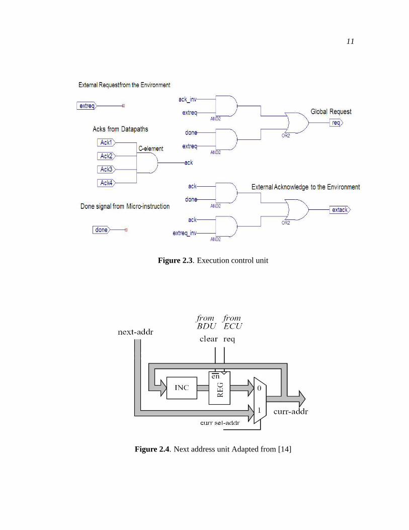
2.3 Execution control unit . . . . . . . . . . . . . . . . . . . . . . . . . . . . . . . . . . . . . . . 11
2.4 Next address unit Adapted from [14] . . . . . . . . . . . . . . . . . . . . . . . . . . . . 11
2.5 Branch detect unit . . . . . . . . . . . . . . . . . . . . . . . . . . . . . . . . . . . . . . . . . . 12
2.6 Local RAS block . . . . . . . . . . . . . . . . . . . . . . . . . . . . . . . . . . . . . . . . . . . 13
2.7 IP header format . . . . . . . . . . . . . . . . . . . . . . . . . . . . . . . . . . . . . . . . . . . . 13
2.8 Ethernet frame format . . . . . . . . . . . . . . . . . . . . . . . . . . . . . . . . . . . . . . . 15
2.9 Click modular IP router configuration Adapted from [18] . . . . . . . . . . . . . 17
3.1 High level architecture of the microengine-based router . . . . . . . . . . . . . . 23
3.2 Block diagram of ingress microengine . . . . . . . . . . . . . . . . . . . . . . . . . . . 26
3.3 Send-to-fifo datapath . . . . . . . . . . . . . . . . . . . . . . . . . . . . . . . . . . . . . . . . 27
3.4 Block diagram of IP header processing microengine . . . . . . . . . . . . . . . . . 29
3.5 Alt-ring conditional construct . . . . . . . . . . . . . . . . . . . . . . . . . . . . . . . . . . 33
4.1 Datapath execution in the 6th microinstruction of IP header processingmicroengine . . . . . . . . . . . . . . . . . . . . . . . . . . . . . . . . . . . . . . . . . . . . . . . 37
4.2 Microinstruction execution times of ingress microengine . . . . . . . . . . . . . 38
4.3 Microinstruction execution times of IP header processing microengine . . . 39
B.1 Source code of a 2-input c-element . . . . . . . . . . . . . . . . . . . . . . . . . . . . . . 59
B.2 Source code of IP-header processing microengine’s BDU . . . . . . . . . . . . . 60
B.3 Source code of next-address logic . . . . . . . . . . . . . . . . . . . . . . . . . . . . . . . 61
B.4 Source code of next-address logic contd. . . . . . . . . . . . . . . . . . . . . . . . . . 62
B.5 Source code of IP-header processing microengine’s microinstruction register 63
B.6 Source code of sel-addr toggle module . . . . . . . . . . . . . . . . . . . . . . . . . . . 64
B.7 Source code of the address register . . . . . . . . . . . . . . . . . . . . . . . . . . . . . . 65
B.8 Source code of the 8-bit ALU . . . . . . . . . . . . . . . . . . . . . . . . . . . . . . . . . . 66
B.9 Source code of the 16-bit ALU . . . . . . . . . . . . . . . . . . . . . . . . . . . . . . . . . 67
B.10 Source code of the 16-bit comparator . . . . . . . . . . . . . . . . . . . . . . . . . . . . 68

B.11 Source code of the 16-bit comparator contd . . . . . . . . . . . . . . . . . . . . . . . 69
B.12 Source code of the RAS block with set-exe . . . . . . . . . . . . . . . . . . . . . . . . 70
B.13 Source code of the RAS block with set-exe and set-seq . . . . . . . . . . . . . . . 71
B.14 Source code of the RAS block with set-seq . . . . . . . . . . . . . . . . . . . . . . . . 72
B.15 Source code of the RAS block with multiple set-seq bits and set-exe . . . . . 73
ix

LIST OF TABLES
4.1 Microinstruction execution times of an ingress microengine . . . . . . . . . . . 37
4.2 Microinstruction execution times for IP header processing microengine . . 38
4.3 Ingress microengine per packet execution time . . . . . . . . . . . . . . . . . . . . . 40
4.4 IP header processing microengine per packet execution time . . . . . . . . . . . 40
4.5 The number of datapaths executing in the IP header processing microengine 41
4.6 The number of datapaths executing in the ingress microengine . . . . . . . . . 42
4.7 Click element’s per packet execution time . . . . . . . . . . . . . . . . . . . . . . . . 43
A.1 Address register’s microcode . . . . . . . . . . . . . . . . . . . . . . . . . . . . . . . . . . 48
A.2 8-bit ALU’s microcode . . . . . . . . . . . . . . . . . . . . . . . . . . . . . . . . . . . . . . . 49
A.3 Offset register’s microcode . . . . . . . . . . . . . . . . . . . . . . . . . . . . . . . . . . . . 49
A.4 Packet memory’s microcode . . . . . . . . . . . . . . . . . . . . . . . . . . . . . . . . . . . 49
A.5 Header register’s microcode . . . . . . . . . . . . . . . . . . . . . . . . . . . . . . . . . . . 50
A.6 16-bit comparatorA’s microcode . . . . . . . . . . . . . . . . . . . . . . . . . . . . . . . . 50
A.7 16-bit comparatorB’s microcode . . . . . . . . . . . . . . . . . . . . . . . . . . . . . . . . 50
A.8 Flow-id register’s microcode . . . . . . . . . . . . . . . . . . . . . . . . . . . . . . . . . . 51
A.9 Send-to-fifo’s microcode . . . . . . . . . . . . . . . . . . . . . . . . . . . . . . . . . . . . . 51
A.10 Global control microcode . . . . . . . . . . . . . . . . . . . . . . . . . . . . . . . . . . . . . 51
A.11 Microcode for IP microengine’s address and paint registers . . . . . . . . . . . 52
A.12 Microcode of IP microengine’s 8-bit ALU . . . . . . . . . . . . . . . . . . . . . . . . 53
A.13 Microcode of IP microengine’s packet store . . . . . . . . . . . . . . . . . . . . . . . 53
A.14 Microcode of IP microengine’s header register file . . . . . . . . . . . . . . . . . . 54
A.15 Microcode of IP microengine’s header register file contd. . . . . . . . . . . . . . 55
A.16 Microcode of IP microengine’s 16-bit ALU . . . . . . . . . . . . . . . . . . . . . . . 55
A.17 Microcode of IP microengine’s 16-bit comparator . . . . . . . . . . . . . . . . . . . 56
A.18 Microcode of IP microengine’s 16-bit temporary registers . . . . . . . . . . . . 56
A.19 Microcode of IP microengine’s CAMs and send-to-fifo datapaths . . . . . . . 57

A.20 Microcode of IP microengine’s flow-id register . . . . . . . . . . . . . . . . . . . . . 58
A.21 Microcode of IP microengine’s global control . . . . . . . . . . . . . . . . . . . . . . 58
xi

ACKNOWLEDGMENTS
The three years that I have spent as a masters student has been one of the most
rewarding experiences of my life. I not only furthered my technical skills but also got
an opportunity to enrich my personal life. I have realized the importance of patience,
intellectual humility and optimism during this course of time. My masters at Utah has
influenced me to pursue a doctorate in the department and has equipped me better for
future challenges.
I would like to sincerely thank my advisor Erik Brunvand for guiding me towards the
completion of this thesis. He has been very encouraging and patient with me besides
giving me a lot of independence. I am grateful to him for giving me opportunities
to attend many conferences. I would like to thank my committee members, Ganesh
Gopalakrishnan and Al Davis for their constructive and timely feedback on my proposal
and thesis drafts that has helped strengthen my thesis evaluation.
I am grateful to my colleagues: Vamshi, Himanshu and Gaurav for insightful techni-
cal discussions and help with CAD tool troubleshooting. Special thanks to my graduate
advisor Karen Feinauer for readily helping out with all the paper work and last minute
requests.
Thanks to my parents for always having faith in my abilities and being my role
models for pursuing a career in research and teaching. Thanks to all my friends (nu-
merous to name here) for their friendship, support and being my family during my stay
in Utah. Finally, special thanks to my life partner Shashi for all his love, wisdom and
encouragement that has helped me cope with difficult times.

CHAPTER 1
INTRODUCTION
Programmable controllers have gained a widespread popularity in varied processing
fields as they give the designers the advantages of allowing correction of errors in later
stages of design cycles, flexibility, easy upgrading of product families, meeting time to
market etc. without compromising much on performance. There are many examples
of synchronous programmable controllers like the ones in the FLASH processor[19],
S3MP processor[1] and many commercial ASICs (Application-Specific Integrated Cir-
cuit). Although traditional programmable controllers are synchronous, there is no reason
that such controllers could not also be designed in an asynchronous style. Asynchronous
implementation could add extra features that designers could exploit to improve their
systems. For example, asynchronous programmable control in the form of a micro-
programmed asynchronous controller (also known as asynchronous microengine[13, 14,
12]) provides modular and easily extensible datapath structures along with high perfor-
mance by exploiting concurrency between operations and employing efficient control
structures. These microengines are programmable at the fine granularity of microcode
and are close in performance to ASICs. Other than the modularity and flexibility ad-
vantages, microengines help exploit other aspects of asynchronous design style like low
power consumption and low EMI. Asynchronous microengines have been around for
quite some time but haven’t been actively pursued in realistic domains. The focus of this
thesis is to evaluate an asynchronous microengine based architecture in the domain of
network processing.
Traditionally, most networking functions above the physical layer have been im-
plemented by software running on general-purpose processors or there have been spe-
cialized ASICs for these tasks. ASICs provide an expensive solution and give a good
2
performance but lack flexibility and programmability whereas general-purpose proces-
sors provide programmability at the cost of performance. The bandwidth explosion in
the past couple of years has resulted in more bandwidth-hungry and computationally
intensive applications like VoIP (Voice over Internet Protocol), streaming audio and
video, P2P(Peer to Peer) applications etc. For networks to effectively handle these new
applications, they will need to support new protocols along with high throughput and
hence the need for flexible and modular network processing equipment. Initially, the
layer 2 and layer 3 processing was hard-wired but, after rapid changes in lower layer
protocols and higher layer’s applications, a more scalable solution in the form of network
processors[5, 26] has emerged. These network processing units have been optimized
for networking applications and combine the advantages of ASIC and general purpose
processors. There has been a wide range of programmable architectures proposed for
network processing. This thesis has proposed an asynchronous-microengine based cir-
cuit style which can also be one of the solutions as it fits into the domain of network
processing naturally. It does this by exploiting the asynchrony in network packet flow
along with a highly flexible, modular and extensible architecture. Although the present
network processor design approach is to balance programmability and performance, the
existing solutions are still limited by the memory bottleneck issues and are not dealing
with power consumption problem. This thesis does not deal with the memory bottleneck
but helps alleviate power consumption by providing the equivalent of clock gating at a
fine-grain level because of the asynchronous behavior of the circuits.
In this work, a case for asynchronous microengines in the domain of network pro-
cessing is presented. This circuit style has been evaluated by demonstrating fast-path
IP (Internet Protocol) routing as the packet processing application. Two types of mi-
croengines have been designed, namely ingress and IP-header processing microengines.
The ingress microengine does packet classification while the IP-header processing micro-
engine performs various functions on the IP header like TTL (time to live) decrement,
checksum check and computation, etc. Each microengine core is specialized enough
for different packet processing kernels yet, generic enough to handle newer protocols

3
and applications. The flexibility aspect of this design has been demonstrated by adding
firewalling functionality to the router by modifying the microcode.
These microengine cores can be used to replace RISC cores or can be used as co-
processors. The asynchronous design style makes it possible to have a large number of
these cores on a single chip without having to worry about clock interface issues. An
asynchronous core can also be easily integrated with a synchronous system using FIFO
interfaces.
To shorten the design cycle time, this design has been implemented on a Xilinx
xs2S150 SpartanII FPGA [32] board. Since a microprogrammable architecture’s real
benefit is to help designers re-program the ASIC by changing the microcode, an FPGA
implementation of a microprogrammable design has no advantage as it is already recon-
figurable. Thus, for most of the evaluation of this design approach, an extrapolated ASIC
version has been used. This architecture’s per-packet computation performance has been
compared with the Click software router[18].
This thesis
• Demonstrates that the asynchronous microengines are well-suited to network-processing
• Implements a modular IP router that does minimal data-plane processing and pro-
totype it on a Xilinx FPGA board
• Evaluates its performance by measuring the execution times for various packet
types and comparing it to a similar Click Router configuration
• Extrapolates the performance to best guess ASIC

CHAPTER 2
BACKGROUND
In this chapter, the asynchronous design [6, 21] approach is briefly introduced, the
motivation behind using this approach is discussed along with the asynchronous micro-
engine architecture, routing concepts and the Click software router [18].
2.1 Asynchronous Design
Asynchronous, or self-timed, systems are those that are not subject to a global syn-
chronizing clock. Since asynchronous circuits have no global clock, they must use some
other means to enforce sequencing of circuit activities. These sequencing techniques
can range from using a locally generated, clock-like signal in each submodule to em-
ploying handshake signals both to initiate (request) and detect completion of submodule
activities (acknowledge), and many variations in between. Circuits that use handshakes
to sequence operations are known as self-timed circuits [25] and allow control to be
distributed throughout the circuit instead of centralized in a controller. For asynchronous
control, the two dominant handshaking protocols are:
two-phase (transition) signaling in which each transition on REQ or ACK signals rep-
resents an event.
four-phase (level) signaling in which only positive-going transition on REQ or ACK
signals initiates an event and each signal must be “returned to zero” before the
handshake cycle is completed.
A self-timed system thus, consists of self-timed modules that are communicating with
each other in parallel or in sequence using these handshake protocols. In this imple-
mentation, the four-phase handshaking protocol has been used that is very similar to

5
synchronous design style so that the synchronous memory modules available in the
Xilinx library can be utilized easily.
2.2 Advantages of Asynchronous DesignIn the network processing domain, asynchronous systems have a number of com-
pelling advantages over their synchronous counterparts, including:
Timing Self-timed circuits separate timing from functionality. Rather than synchronize
the entire system to a global clock signal, self-timed circuits localize timing in-
formation to individual circuits and avoid the problems of clock distribution and
clock skew endemic in synchronous designs.
Composability Systems may be constructed by connecting components and assembling
subsystems based only on their functionality rather than having to consider their
timing characteristics. Each subsystem can be designed and tested independently
with confidence that, because a self-timed communication protocol is used, they
will operate correctly when assembled into a larger system. This enables us to use
network processing microengines along with other processors on SOC (System on
a chip).
Lower Power Dissipation As clock speed and system size increase, the portion of the
system’s power budget dedicated to distributing the clock increases dramatically.
Self-timed systems do not incur the power overhead of distributing a free running
clock across the entire system. Because self-timed systems make signal transitions
only when actually doing work or communicating, large systems can show greatly
decreased power dissipation in some technologies (like CMOS), especially during
quiescence. Due to reactive reactive nature of network packets, we can have a
natural power down during slack times.
Lower Electromagnetic Interference (EMI) A free running clock signal charges and
discharges large capacitances (the clock tree is typically the largest and most capac-
itive net on a chip) at regular intervals. This is a source of a great deal of EMI and
can have serious consequences, especially for circuits that have RF components.
6
Self-timed systems may make just as many transitions as a clocked system, but
those transitions are uncorrelated in time so they do not lead to the bad EMI
properties of synchronous circuits. Also, local handshake wires tend to have lower
capacitance than a global clock line. This can be an advantage as the network
routers can be in proximity to other RF type devices.
Incremental Improvement In a properly designed asynchronous system it is possible
to improve the performance or functionality of a system by improving or replac-
ing individual subsystems incrementally without changing or re-timing the whole
system. This can be an advantage by allowing plug-in modules for newer versions
of protocols.
Performance Traditional synchronous systems usually exhibit worst case behavior while
asynchronous systems tend to reflect the average case. This difference can result in
large performance increases for some systems. Since most of the network packets
are average cases, we can get higher performance.
2.3 Asynchronous Microengine
An asynchronous microengine is a microprogrammed self-timed controller which
allows per-microinstruction programmability of its datapath topology by arranging its
datapaths in series and parallel clusters. This feature allows the parallel clusters to run
concurrently while allowing the serial units within a cluster to chain. This chaining
of operations is possible due to explicit acknowledge generation by each asynchronous
datapath in the sequence. Chaining reduces the control overhead as it reduces the number
of microinstructions by combining several microinstructions into a single VLIW type
instruction. This is very hard to implement for synchronous designs as the propagation
delay of serial partitions of combinational modules must add up to be an integral multiple
of clock period.

7
2.3.1 Architecture Overview
A conventional (synchronously clocked) microprogrammed control structure consists
of a microprogram store, next address logic, and a datapath. Microinstructions form
commands applied on the datapath and control flow is handled by the next address logic
that, with the help of status signals fed back from the datapath, generates the address
of the next microinstruction to be executed. In a synchronous realization the execution
rate is set by the global clock which must take the worst case delay of all units into
account. When the next clock edge arrives it is thus assumed that the datapath has
finished computing and the next address has been resolved, and the next microinstruction
can be propagated to the datapath. The asynchronous microengines have an organization
similar to those of conventional synchronous microprogrammed controllers. However,
as shown in Figure 2.1, the major difference between the synchronous microprogrammed
structure and an asynchronous microprogrammed structure is the request-acknowledge
handshake between the datapaths and the execution control unit instead of being driven
in lock-step by a global clock.
Figure 2.1. Microengine’s high level structure

8
In conventional synchronous microprogrammed controllers, the computation is started
by an arriving clock edge and the datapath is assumed to have completed by the following
clock edge. In the asynchronous case we have no clock to govern the start and end of an
instruction execution. Instead a request is generated to trigger the memory to latch the
new microinstruction and the datapath units to start executing. The memory and each
datapath unit then signals their completion by generating an acknowledge.
2.3.2 Microengine Execution
A microengine starts its execution on receiving an external request from the environ-
ment. The execution control unit in response to this request generates a global request
that latches the first or the specified microinstruction from the microprogram and also
causes the datapaths that are set up for execution to start executing. The microcode
consists of fields that specify which datapath has been setup for execution and in what
mode, i.e. ,sequential or parallel with respect to other datapaths, and multiplexer select
signals which specify the input data and output data for that particular microinstruction.
On completion of computation, the datapaths generate acknowledges which are sent
back to the execution control unit. Meanwhile, the branch detect unit evaluates the
conditional signals generated by the datapath and determines the address of the next
microinstruction to be executed. After gathering the acknowledges, the execution control
unit checks to see if the done bit (one of the global control fields in the microcode) is
high which specifies that the operation desired by the environment is completed and
sends an external acknowledge signal to the environment and awaits the next invocation,
otherwise it executes the next microinstruction and repeats the global request-generation
cycle.
2.3.3 Next Address Generation
The next microinstruction is fetched in parallel to the execution of the current mi-
croinstruction to increase performance and hide control overhead. This approach works
smoothly except when branches are involved. The problem of branch-prediction is solved
by fetching the next microinstruction but not committing it until the address selection is

9
resolved. The designer programs each branch to be taken or not taken on studying the
probability for each case using empirical data. The next-address logic is kept simple by
storing the next address in the case of a branch instruction in the microinstruction itself
and a delay slot is used to store the next microinstruction supposedly to branch to or the
next sequential microinstruction depending on the predicted branch selection strategy.
2.3.4 Microcode Fields
Figure 2.2 shows the various fields of a microinstruction (all fields are not shown
in this figure). The microcode fields control the local operation mode of each datapath
and control the global microprogram flow. Amongst the local control fields, the set-exe
or se bit controls whether the particular datapath unit will execute during the current
request cycle or not and the set-seq or ss bit controls whether it will execute in sequential
(chained) mode or parallel mode. If a datapath always executes in the sequential mode,
then the se can be used to incorporate ss functionality. The set-mux and op fields deter-
mine which operands and operation the given datapath should use. The en bits enable
which registers when there are multiple registers in a datapath, should latch data.
The following global control fields control the flow of the microprogram. The set-
branch bit specifies whether this microinstruction is a branch instruction or not and on
Figure 2.2. Microinstruction format

10
which conditional expression, the branch should be tested. The next-addr field specifies
the branch-address. The bra-pred bit specifies the branch-prediction strategy for the
branch instruction i.e whether this branch has been predicted to be taken or not. The eval
bit specifies whether it’s a conditional branch or a jump instruction. The sel-addr bit
selects either next sequential microinstruction or the branch instruction. If the microin-
struction is not a branch instruction then next-addr, bra-pred, eval and sel-addr bits are
dont-cares. Finally, the done bit specifies whether it is the last microinstruction or not
and signals the execution control unit that the microprogram computation is over and the
results are available on the output ports.
For example in the Figure 2.2, there are two datapaths A and B whose set- signals
are shown. In the first microinstruction, only A has been set to execute whereas in the
second microinstruction, both A and B execute and both operate in parallel mode. In the
microinstruction, both A and B execute but B executes in sequential mode with respect
to A. This microinstruction is also a branch instruction where the results of datapath A
evaluate the branch condition and this branch has been predicted to be not taken.
2.3.5 Control Units
The global control units for a microengine are:
1. ECU: The Execution Control Unit generates the global request signal apon receiv-
ing an external request. It then synchronizes all datapath acknowledges. It keeps
repeating the generation of request signal until it sees a high done signal and then
generates an external acknowledge. The block level implementation figure for an
ECU is shown in Figure 2.3.
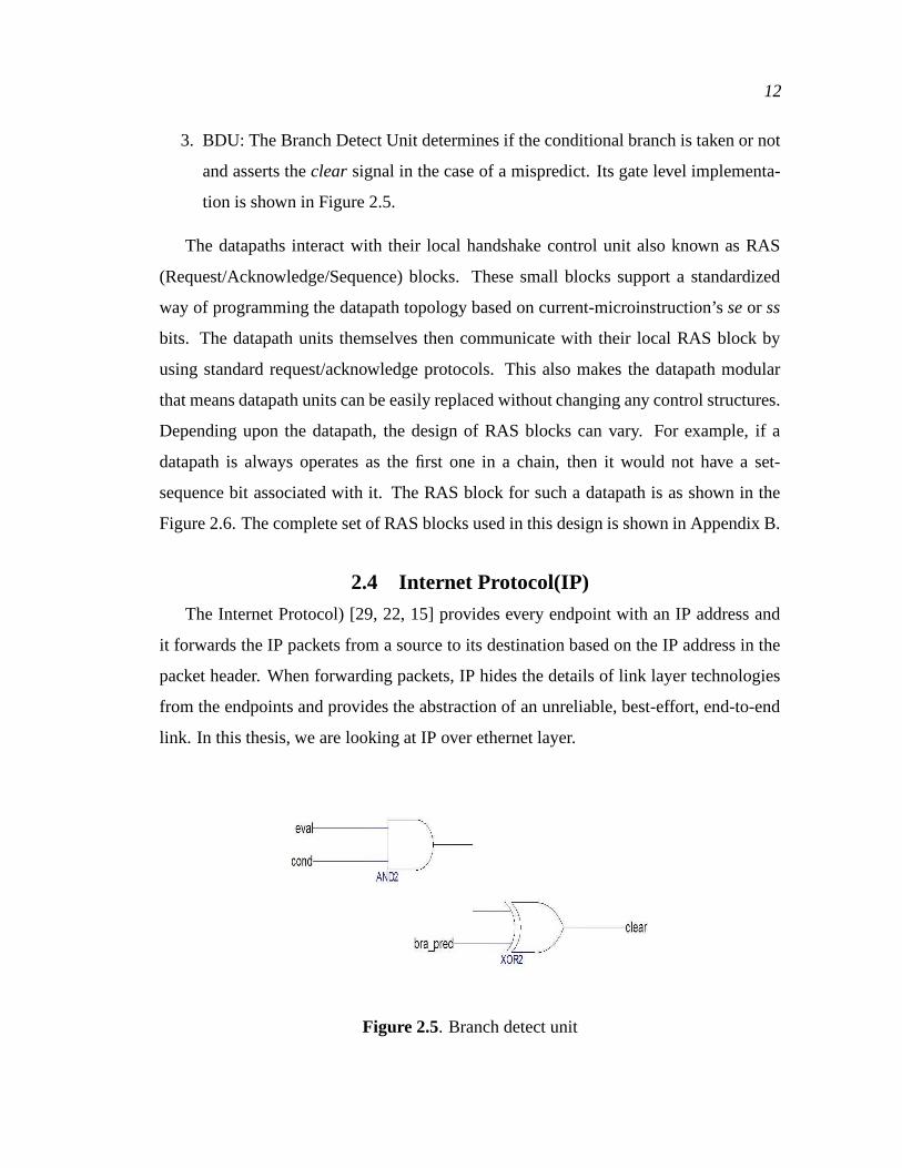
2. Next Address Unit: This control unit is used to compute the address of the microin-
struction predicted to execute next at the start of next execution cycle. Figure 2.4
shows the block level implementation of this unit. The current value of the sel-addr
bit is the conditional input to the mux for selecting the next address. In the case
of a branch mispredict, BDU asserts the clear signal which then toggles the value
of sel-addr bit from the memory and the current microinstruction is latched in the
next execution cycle.
11
Figure 2.3. Execution control unit
Figure 2.4. Next address unit Adapted from [14]
12
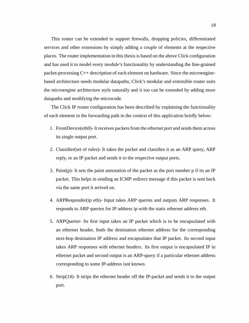
3. BDU: The Branch Detect Unit determines if the conditional branch is taken or not
and asserts the clear signal in the case of a mispredict. Its gate level implementa-
tion is shown in Figure 2.5.
The datapaths interact with their local handshake control unit also known as RAS
(Request/Acknowledge/Sequence) blocks. These small blocks support a standardized
way of programming the datapath topology based on current-microinstruction’s se or ss
bits. The datapath units themselves then communicate with their local RAS block by
using standard request/acknowledge protocols. This also makes the datapath modular
that means datapath units can be easily replaced without changing any control structures.
Depending upon the datapath, the design of RAS blocks can vary. For example, if a
datapath is always operates as the first one in a chain, then it would not have a set-
sequence bit associated with it. The RAS block for such a datapath is as shown in the
Figure 2.6. The complete set of RAS blocks used in this design is shown in Appendix B.
2.4 Internet Protocol(IP)
The Internet Protocol) [29, 22, 15] provides every endpoint with an IP address and
it forwards the IP packets from a source to its destination based on the IP address in the
packet header. When forwarding packets, IP hides the details of link layer technologies
from the endpoints and provides the abstraction of an unreliable, best-effort, end-to-end
link. In this thesis, we are looking at IP over ethernet layer.
Figure 2.5. Branch detect unit

13
Figure 2.6. Local RAS block
2.4.1 IP Header
As seen from the Figure 2.7, the IP header without options consists of 20 bytes
and with options can be an additional 40 bytes. The various fields of an IP header are
explained below:
4-bit Header Length This field specifies the length of the header in 4-byte words and
automatically translates to a limit of 60 bytes. The header length field allows a
router or host to distinguish between header and payload.
Figure 2.7. IP header format

14
4-bit Version The current IP version is 4 (a.k.a IPv4). This field allows the upgraded
version 6 (IPv6) to coexist with IPv4.
Type of Service(TOS) This field is composed of a 3-bit precedence field(which is ig-
nored today), 4 TOS bits and an unused bit which always 0. The four TOS bits
are: minimize delay, maximize throughput, maximize reliability, and minimize
monetary cost. Only one of these four bits can be turned on. The TOS feature is
not supported by most TCP/IP implementations today.
Total Length This field specifies the total length of an IP datagram in bytes. Since it is
16-bits long, the longest IP packet is 65,535 bytes long.
Identification It uniquely identifies an IP packet among those that have a given source
and destination address.
3-bit Flags This field supports fragmentation. Only 2 out of 3 bits are significant. One
of the flags is “More fragments”. If this flag is set to 1 then the router or host
knows that there are more fragments arriving before it does a reassembly and it
waits untill it receives a datagram with this flag set to 0. The other flag is “Don’t
fragment”. If this flag is set, the router which gets a packet whose size is too large
for its next hop must discard it.
Fragment offset This field also supports fragmentation and reassembly. It tells the
destination which part of the original packet is contained in the current fragment.
Time-To-Live This field gets decremented at every hop and thus helps to control the
lifetime of a packet. If it becomes zero, then the packet is discarded.
Protocol This field tells IP to which upper layer protocol it should pass the packet. It is
typically TCP or UDP.
Header Checksum This field protects against the corruption in the packet header. IP
does not checksum data. To compute the checksum for an outgoing packet, the
value of the field is set to zero. Then the 16-bit one’s complement sum of the

15
entire header is calculated and this value is stored in the checksum field. When
an IP datagram is received, the 16-bit one’s complement sum of header is calcu-
lated. Since the receiver’s calculated checksum contains the checksum stored by
the sender, the receiver’s checksum is all one bits if nothing in the header was
modified. If the result is not all one bits (checksum error), IP discards the packet.
32-bit Source IP address This field is used to send a reply to the source of the packet
such as when any error is generated.
32-bit Destination IP address This field is used to route the packet and forward it to its
destination.
Options These options are not universally implemented in the Internet and are not a
common case. To save packet processing time, many high speed routers do not
process options. In this thesis, we are not processing options.
2.4.2 IP Over Ethernet Layer
Ethernet [29] is the most commonly used link layer protocol for LANs and is fre-
quently used to support a range of network layer protocols, including IP. The IP data-
grams are transmitted by encapsulation in Medium Access Control (MAC) frames. IP
introduces an extra protocol, known as the address resolution protocol (ARP) to map
between the destination hardware 48-bit address in a MAC frame and a 32-bit IP address.
In this thesis, we classify the packets at the ethernet layer as ARP query, ARP reply and
IP packet but do not process the ARP packets. As shown in Figure 2.8, the type field is
used for this classification.
Figure 2.8. Ethernet frame format

16
2.4.3 IP Router
A router [8, 16] is defined as a host that has an interface on more than one network.
Every router along the path has a routing table with at least two fields: a network number
and the interface on which to send packets with that network number. When a router
receives a datagram, it looks up the routing table to determine its next-hop address and
forwards it to the outgoing port. If the destination address is unknown, then it sends
the packet to the default route. IP routing consists of data-plane processing and control-
plane processing. Data-plane processing comprises of packet processing tasks such as
ttl decrement, checksum check and checking other fields in the IP header such as header
length etc. and datagram forwarding by doing a route lookup. Control-plane processing
consists of generating ICMP error messages and handling of routing protocols which
decide which path is best to reach a destination and corresponding routing table updates.
In this thesis, an IP router has been implemented which does data-plane processing and
does not handle any control-plane processing.
2.5 Click Modular Router
Click is a software architecture for building flexible and configurable routers that
was developed at MIT[17]. Applications in Click are built by composing modules called
elements which perform simple packet-processing tasks like classification, route-lookup,
header verification, queuing, scheduling and interfacing with network devices. A click
configuration is a directed graph with elements as vertices; packets flow along the edges
of the graph. Click is implemented on Linux using C++ classes to define elements. Ele-
ment communication is implemented with virtual function calls to neighboring elements
and connections are represented as pointers to element objects. These configurations are
modular and easy to extend.
This thesis has looked into the Click IP router configurations given in [18]. A stan-
dard IPv4 over ethernet bridge router with two network interfaces has sixteen elements
in its forwarding path. Figure 2.9 shows an IP router’s configuration.

17
Figure 2.9. Click modular IP router configuration Adapted from [18]
18
This router can be extended to support firewalls, dropping policies, differentiated
services and other extensions by simply adding a couple of elements at the respective
places. The router implementation in this thesis is based on the above Click configuration
and has used it to model every module’s functionality by understanding the fine-grained
packet-processing C++ description of each element on hardware. Since the microengine-
based architecture needs modular datapaths, Click’s modular and extensible router suits
the microengine architecture style naturally and it too can be extended by adding more
datapaths and modifying the microcode.
The Click IP router configuration has been described by explaining the functionality
of each element in the forwarding path in the context of this application briefly below:
1. FromDevice(eth0)- It receives packets from the ethernet port and sends them across
its single output port.
2. Classifier(set of rules)- It takes the packet and classifies it as an ARP query, ARP
reply, or an IP packet and sends it to the respective output ports.
3. Paint(p)- It sets the paint annotation of the packet as the port number p if its an IP
packet. This helps in sending an ICMP redirect message if this packet is sent back
via the same port it arrived on.
4. ARPResponder(ip eth)- Input takes ARP queries and outputs ARP responses. It
responds to ARP queries for IP address ip with the static ethernet address eth.
5. ARPQuerier- Its first input takes an IP packet which is to be encapsulated with
an ethernet header, finds the destination ethernet address for the corresponding
next-hop destination IP address and encapsulates that IP packet. Its second input
takes ARP responses with ethernet headers. Its first output is encapsulated IP in
ethernet packet and second output is an ARP-query if a particular ethernet address
corresponding to some IP-address isnt known.
6. Strip(14)- It strips the ethernet header off the IP-packet and sends it to the output
port.

19
7. CheckIPheader()- It takes IP packets as inputs; discards packets with invalid IP
length, source address or checksum fields and forwards valid packets unchanged.
8. GetIPAddress()- Input takes IP packets and copies the IP header’s destination ad-
dress field into the destination IP address variable for that packet; forwards packets
unchanged.
9. LookupIPRoute()- Input takes IP packets with valid destination address variables.
It has arbitrary number of outputs. It looks up input packet’s destination address
variable in a static routing table and forwards each packet to the outport port
specified in the resulting routing table entry;sets its destination address variable
to the resulting gateway address, if any.
10. Dropbroadcasts()- Input takes any packet and discards packets that arrived as link-
level broadcasts and forwards others unchanged.
11. Checkpaint(p)- Input takes any packet and forwards the packet with paint variable
p to both outport ports else only to the first output. The second output port sends
an ICMP redirect message.
12. ICMPError(ip, type, code)- Input takes IP packets, output emits ICMP error pack-
ets. It encapsulates first part of input packet in ICMP errorheader with source
address ip, error type type, and error code code and sets the fix IP Source variable
for this packet.
13. IPGWOptions()- Input takes IP packets. This element processes IP record route
and timestamp options;packets with invalid options are sent to second output.
14. FixIPSrc(ip)- Input takes IP packets and sets the IP header’s source address field to
the static IP address ip if the packet’s fix source variable is set and forwards other
packets unchanged.
15. DecIPTTL- Input takes IP packets and decrements input packet’s IP time to live
field. If the packet is still live, it incrementally updates the checksum and sends the
20
modified packet to the first output; if it has expired, it sends the unmodified packet
to second output.
16. IPFragmenter(MTU)- Input takes IP packets. It fragments IP packets larger than
MTU;sends fragments, and packets smaller than MTU to first output. Too large
packets with dont-fragment-bit set high are sent to the second output.
17. Todevice(eth0)- Input takes ethernet packets for transmission; no outputs.
2.6 Related Work
2.6.1 Programmable Asynchronous Controllers
Programmable asynchronous controllers were looked at in the 1980s [28] in the
context of data-driven machines. They used a vertical microcode for their microse-
quencer which was used to drive multiple slave controllers along with structured tiling
which introduced considerable control-overhead. It was also not an application-specific
controller. In 1997, Jacobson and Gopalakrishnan at Utah looked into the design of
efficient application-specific asynchronous microengines [13, 14, 12]. Their architec-
ture uses a horizontal microcode that allows per-microinstruction programmability of its
datapath topology by arranging its datapath units into series-parallel clusters for each
microinstruction.
2.6.2 Network Processors
Many industries have ventured into Network Processor design and hence, there is
a wide variety of architectures available in the market. However, all designs have one
key point in common: they use multiple programmable processing cores or engines
(PPE) in a single chip. For example, Intel IXP1200 consists of six microengines1 on
a single die but the amount of functionality in these cores varies from vendor to ven-
dor. Some use RISC cores with added bit-manipulation instruction-set also known as
ASIP(Application-Specific Instruction-set Processor), whereas others use a VLIW-based
architecture. In these architectures, multiple PPEs can process in parallel, pipeline or
1The similarity in the name of IXP “microengine” and asynchronous microengines is coincidental

21
combination of both styles depending on the application. However, a RISC-based archi-
tecture is more flexible and easy to configure compared to VLIW(Very Large Instruction
Word)-based architecture. Many RISC-based architectures use multithreading in each
core to maximize throughput and do useful work while there is a wait for the operation
to complete. This is particularly useful to hide memory access latency. Network pro-
cessors that are RISC-based provide dedicated and specialized hardware or integrated
co-processors to perform common network processing tasks like encryption, lookup,
classification, CRC computation, etc.
CHAPTER 3
DESIGN AND IMPLEMENTATION
3.1 Router Architecture
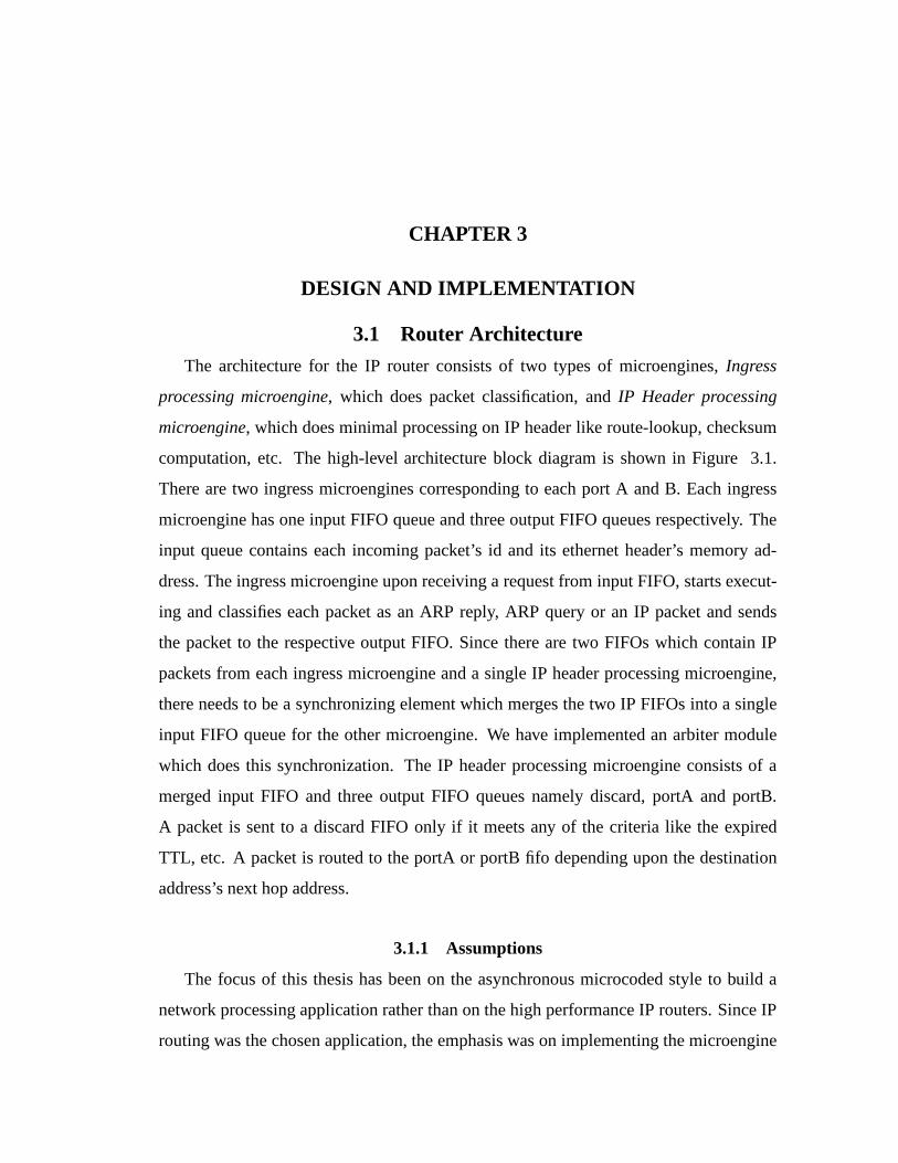
The architecture for the IP router consists of two types of microengines, Ingress
processing microengine, which does packet classification, and IP Header processing
microengine, which does minimal processing on IP header like route-lookup, checksum
computation, etc. The high-level architecture block diagram is shown in Figure 3.1.
There are two ingress microengines corresponding to each port A and B. Each ingress
microengine has one input FIFO queue and three output FIFO queues respectively. The
input queue contains each incoming packet’s id and its ethernet header’s memory ad-
dress. The ingress microengine upon receiving a request from input FIFO, starts execut-
ing and classifies each packet as an ARP reply, ARP query or an IP packet and sends
the packet to the respective output FIFO. Since there are two FIFOs which contain IP
packets from each ingress microengine and a single IP header processing microengine,
there needs to be a synchronizing element which merges the two IP FIFOs into a single
input FIFO queue for the other microengine. We have implemented an arbiter module
which does this synchronization. The IP header processing microengine consists of a
merged input FIFO and three output FIFO queues namely discard, portA and portB.
A packet is sent to a discard FIFO only if it meets any of the criteria like the expired
TTL, etc. A packet is routed to the portA or portB fifo depending upon the destination
address’s next hop address.
3.1.1 Assumptions
The focus of this thesis has been on the asynchronous microcoded style to build a
network processing application rather than on the high performance IP routers. Since IP
routing was the chosen application, the emphasis was on implementing the microengine

23
Ingress Microengine
Input Q port B
Port A Port B
IP Q IP Q
Merged IP input Q
Arbiter
IP Header ProcessingMicroengine
Ingress Microengine
Discard Q
Arp QueryOutput Q
Arp ReplyOutput Q
Arp Reply Arp QueryOutput Q Output Q
Input Q port A
Port B output QPort A output Q
Figure 3.1. High level architecture of the microengine-based router
based controller rather than the supporting circuitry. Thus, many assumptions have been
made with regard to the supporting circuits needed to realize a complete working model.
1. It has been assumed that a NIC exists that does all the link-layer processing like
encapsulating and decapsulating IP packet with ethernet header.
2. It has been assumed that a port processor exists that handles the memory manage-
ment and performs the following functions:
• Buffers incoming packets into the memory.
• Buffers payload in SDRAM; IP and ethernet layer header in SRAM.
• Maintains the state of each packet by assigning each packet-buffer a packet-
id.
• Passes the header-pointer and packet-id to the ingress microengine.
24
• Receives the outgoing packet’s id and pointer from the output queue of IP
header processing microengine and sends that packet to the corresponding
output port.
3. The microengine-based router does not handle headers with IP options and frag-
mented datagrams as routers connected to the end hosts only need to do this
processing.
4. The packets that need control-plane processing are handed over to some other
processor core that is a reasonable assumption as the percentage of control packets
in the real network traffic is very small and even in the case of the Intel IXP,
the strongARM core is responsible for control-plane processing while the RISC
microengine cores handle data-plane processing.
5. This router does not handle ICMP error generation as compared to the click router
configuration as ICMP is also a part of control-plane processing. The packets that
would generate an ICMP error are discarded into a discard FIFO queue.
6. CAM (Content Addressable Memory) has been used to do route lookup. The first
byte of the destination IP address is used to find a match instead of longest prefix
matching algorithm. This optimization has been done to save on limited on-board
Xilinx SRAM.
7. Each microengine has its own copy of header store. This has been assumed as
Xilinx SpartanII library does not have SRAM with four read ports and one write
port. ASIC vendors like Texas Instruments sell such five port register files. Since
each microengine will be reading or writing a different packet, it is ensured that
none of the microengines will try to read/write into the same memory location.
3.2 Ingress Microengine
Ingress microengine classifies the packets into three types namely, ARP Query, ARP
Reply and an IP packet. The block diagram for an ingress microengine is shown in the
Figure 3.2.

25
3.2.1 Datapaths
This microengine consists of the following datapaths:
1. 8-bit Address register, that stores the packet’s memory address.
2. 8-bit ALU, which calculates the offset address for a particular header field and
header memory.
3. 16-bit Header register, that is byte addressable.
4. 16-bit comparators
5. 2-bit Flow-id register, which stores the packet’s classification result
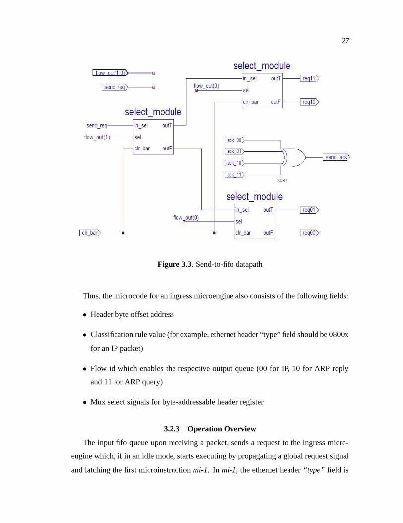
6. Send-to-fifo datapath that enables one of the three output FIFOs by sending them
a request signal based on the flow-id’s value. The block diagram of a send-to-fifo
datapath is shown in Figure 3.3.
7. Header store stores all packet headers.
3.2.2 Microprogram Structure
The microprogram for this microengine consists of four 67-bit wide microinstruc-
tions. Each microinstruction consists of the global control fields such as the branch
address next-addr, done etc. and local control fields for each datapath unit such as
the set-execute se etc. Since flexibility is one of the most important advantages of our
architecture, it is demonstrated by incorporating classification rules in the microcode
itself as this allows for easy upgrading of these rules without needing to change the
underlying hardware. The header bytes that need to be compared with some value can
be specified in the microcode itself along with the rule value.

26
DONE
Microcode Store
Flow−id Reg Send−to−fifo
Packet headerMemory
16−bit Header Register
ECU
BDU
Next−Add
Ack1
Ack4
sreq4
sreq5
sreq4
Header
cmpA flow−id
R A R A R A R A
R R A R A R A
cmpAcmpB
eval bra−pred
Clear
Ext−req
Ext−ack
REQ
sreq1 sreq2 sreq3 sreq4
REQ
sreq7
16−bit 16−bit
Register 8−bit ALU
Ack3
GLOBAL
Ack4
Microcode(66:0)
Header
GLOBAL
Ack2sreq6
A
REQ
sel−addr Branch
Offset Address 32−bit Header
RAS
RAS RAS RAS RAS
GLOBAL
RAS
Comparator A
Ack1
cmpBcmpA
McodeMcode
16−bit
Req to out Fifo
Comparator B
Mcodefrom input fifoAddressPacket
8−bit Address
Mcode
16−bitHeader16−bit
RAS RAS
Add
add
Ack from out Fifo
Out Fifo
Figure 3.2. Block diagram of ingress microengine
27
Figure 3.3. Send-to-fifo datapath
Thus, the microcode for an ingress microengine also consists of the following fields:
• Header byte offset address
• Classification rule value (for example, ethernet header “type” field should be 0800x
for an IP packet)
• Flow id which enables the respective output queue (00 for IP, 10 for ARP reply
and 11 for ARP query)
• Mux select signals for byte-addressable header register
3.2.3 Operation Overview
The input fifo queue upon receiving a packet, sends a request to the ingress micro-
engine which, if in an idle mode, starts executing by propagating a global request signal
and latching the first microinstruction mi-1. In mi-1, the ethernet header “type” field is

28
read out from the memory and then the two comparators check in parallel if the type
is an IP (0800x) or ARP (0806x). If it is an IP packet, then the flow-id “00” from the
microcode gets selected and latched in the flow-id register and the microengine fetches
the next sequential instruction mi-2. If it is an ARP packet, then the flow-id “01” gets
selected and the microengine takes the branch and fetches mi-3. If mi-2 gets executed
then, send-to-fifo datapath is enabled and it sends the packet out to the IP output FIFO
and the microengine jumps to mi-4 which is the done instruction. If mi-3 gets executed
then the ARP “type” field is read from the memory and the two comparators again
compute in parallel to check if it is an ARP reply or query. Depending upon the flow-id
chosen by comparators results, send-to-fifo datapath sends the ARP packet to the reply
or query output FIFOs and fetch the done instruction mi-4. The done instruction sets the
done bit high, upon which the ingress microengine’s ECU sends an ACK to the input
FIFO and waits for the next packet to arrive on this port. In this microengine, most of the
datapath operations are chained except for the parallel comparator evaluation.
3.3 Header-processing Microengine
This microengine buffers the IP-header from the memory into a header register file
and processes it. IP header is then checked if it is valid, i.e, if it has valid “version”
and header length “hlen” fields. The checksum of the incoming packet’s IP header is
computed and then compared it against the “checksum” field. IP header is also checked
for an expired “ttl” field. If the header is valid then the “ttl” field is decremented. The
next hop destination IP address is looked up and the checksum is recomputed and it’s
latest value is written to the checksum field and the packet is sent to the respective port.
If the header was invalid then the packet is discarded by sending it to a discard FIFO.
3.3.1 Datapaths
The block diagram of a IP header processing microengine is shown in Figure 3.4. It
consists mostly of generic data-paths except for CAMs that are specialized for network
processing tasks.

29
sel−addr
Microcode StoreECU
BDU
Next−Add
Add
Clear
Ext−req
Ext−ack
R A
8−bit
R A R A R AR A
16−bit
R A
ONSTANTS
AR
R A R A A R AR
CAMFilter
CAM
lookupRoute
Flow−idReg
Send toFifo
Req to out Fifo
Ack from out Fifo
eval
FileRegHeader
flow−id16−bitTemp
Regs
cmp
Match1cmp
Match2
sreq1 sreq2 sreq4 sreq5
sreq6 sreq7 sreq8sreq9 sreq10
Ack2 Ack3
Ack4
Ack1
Ack5 Ack6 Ack7
REQ
8−bit Header 8−bit Header16−bitALUResult
tempAtempB
DONE
RAS RAS
Match1
Match1
RAS RAS
REQGLOBAL
REQGLOBAL
Microcode(110:0)
sreq9
sreq3
bra−pred
16−bit headerPacket
Memory Comp
C
Ack8
Ack1
Ack8
8−bit ALU
Wport
Rport
Mcode
GLOBAL
McodeAddReg
Packet Add
from input fifo
Mcode
Offset Add
addBranch
sreq7
OutFifo
tempA
tempB16−bitHeader
16−bit
ALU
sreq4 RAS
16−bit
Result
sreq6
Mcode
RAS RAS RAS RAS RAS
RAS
cmp
32−bit Header
Figure 3.4. Block diagram of IP header processing microengine

30
The generic datapaths in this microengine are similar to ingress microengine and
include the 8-bit address register, header memory, 16-bit comparator, 16-bit temporary
registers, 8-bit ALU, 16-bit ALU, flow-id and send-to-fifo datapaths. Amongst the
specialized datapaths, we have one CAM that does route lookup and another one that
implements a stateless firewall. Modularity of datapaths in this architecture has been
demonstrated by adding a filtering (based on source IP address) CAM in our design. The
filtering extension can be disabled by changing the set-exe bit of this datapath in the mi-
crocode to not execute. Since we are the entire IP header (20 bytes without IP options) is
stored in this microengine, the register file has been implemented as a 4-byte wide and 16
word deep dual port SRAM which has one synchronous write port and an asynchronous
read port. This helps in parallelizing the writing of new header bytes into the memory
and reading of already stored bytes for doing checks and checksum computation. It
can be seen that except for CAMs and dual port register file, most of the datapaths are
generic and common to both ingress and IP header processing microengines. Depending
on the design requirement (if chip area is not a constraint), the ingress microengine can
be implemented by changing the IP header processing microengine’s microcode.
3.3.2 Microprogram Structure
There are fifteen 111-bit wide microinstructions for this microengine. The global
and local control microcode fields are same as described earlier. This microprogram has
microcode fields similar to the ingress microengine’s like the flow-id values, read and
write addresses for header bytes, etc. Since there are many constant values that are being
compared to some header bytes like the version field, hlen field etc., these constants
have not been incorporated in the microcode and are being stored in constant registers.
However, if there is a need for more flexibility due to changes in protocol, these constants
can be added as microcode fields.
3.3.3 Operation Overview
The microengine receives an IP packet from the input FIFO and begins its execution
and after it finishes processing, it sends out the packet header address into one of the three
31
output FIFOs (portA, portB and discard). The entire IP header processing algorithm has
been implemented in fifteen microinstructions and there may be opportunities for further
optimizations. Out of fifteen microinstructions, nine microinstructions have two parallel
execution clusters and one microinstruction has three parallel execution clusters. The
first microinstruction mi-1 latches the packet’s memory address in the address register
and then computes the offset address and reads the four header bytes from the packet
memory and writes them to the dual port header register, followed by checking the first
byte to be valid (i.e checking for “version” and header length “hlen” fields). If the check
evaluates to true then the control jumps to mi-3 otherwise the next sequential mi-2 which
is the packet discard microinstruction and sends the packet’s address to discard FIFO and
jumps to mi-15(done) microinstruction. There are three microinstructions in which if any
of the checks fail then the control jumps to the discard microinstruction (mi-2). One of
the interesting features of in this algorithm is the way the checksum of an incoming
packet is being computed. After the first four bytes are written to the register file, the
two 16-bit consecutive header bytes (1,2 and 3,4) are added and stored in a temporary
register. From this point onwards, two header bytes from asynchronous read port are read
and then added to the value stored in temporary register in parallel with writing of header
bytes on the write port. This works as it is ensured that the read and write addresses are
not same. The temporary register keeps getting updated. The 16-bit sum for the entire IP
header except for checksum and ttl fields is stored in a separate temporary register. This
value can later be used to calculate the checksum of the outgoing packet by just adding
the latest ttl field value to it. The writing of latest ttl and checksum values to the header
memory in two microinstructions has also been handled in this implementation.
3.4 Design Methodology
The asynchronous microengine based router architecture has been prototyped on
the Xilinx SpartanII XS2S150 board made by Xess. The design has been validated
with respect to functionality and complete back-annotated timing analysis has been per-
formed. Xilinx ISE tool-suite has been used for synthesis, placement and routing and
MTI Modelsim for simulation. The 3D tool[34] was initially used for the synthesis of
32
execution control unit but it did not give a correct specification and the circuit was then
modified by hand. The block diagram for the ingress microengine is shown in Figure 2.3.
A mixed design flow for the prototyping of this design has been used. Microcode stores
and CAMs have been implemented using Xilinx’s IP cores using Logicore tool. A few
of the datapaths and control units have been designed using a two-phase macromodular
approach while the rest of the datapaths have been specified in behavioral VHDL. The
final assembly has been done in the ISE ECS schematic capture environment. The
abovementioned various design flows have been explained in the following subsections.
3.4.1 Macro-modular Design Approach
Self-timed macro-modules have been used for designing a few of the control and
datapath elements [3]. To accomplish this, a subset of two-phase control modules for
the Xilinx FPGA were designed which consisted of the following: C-element, transition
latch, select, q-select, toggle and two-way call element. The C-element was coded in
behavioral VHDL whereas the rest of the elements were designed using xilinx compo-
nents in the ISE ECS schematic editor. These macromodules have been used to build
self-timed flow-through FIFOs [30]. Since this design uses a four-phase handshaking
protocol, protocol converters have been used to interface these macro-module based
two-phase designs with the four-phase implementation. The Send-to-fifo datapath has
been designed using these modules(Select). Our arbiter circuit is based on a q-select ring
alt construct which also uses these modules as shown in Figure 3.5.
3.4.2 VHDL-based Design Approach
Most of the datapaths such as the ALUs, comparators, registers and control units such
as all the RAS blocks have been specified using behavioral VHDL. These VHDL specifi-
cations have been verified functionally using Modelsim simulator. Most of these modules
are not optimized for high-performance. Various interesting high-speed circuit-design
styles can offer a much better performance if this design was not being implemented on
an FPGA.

33
Figure 3.5. Alt-ring conditional construct
3.4.3 Memory Design Using Xilinx Core Generator
The microcode stores, header store, dual-port header register and CAMs [33] have
been designed using Xilinx cores. These cores are optimized for high-performance and
can be easily integrated into a VHDL, Verilog or a schematic-based design flow. These
cores give users the flexibility to define features such as the memory depth, width, option
of RAM or ROM and the type of on-chip memory resources to be used (distributed
SelectRAM or blockRAM) etc. The Xilinx Logicore tool (Core generator) helps specify
the initial contents of memory using a memory editor tool. The memory editor tool
allows a user to specify the initial contents in an array format. This is of immense utility
when compared to specifying the contents using the INIT attributes in terms of ease and
flexibility. For a microcoded framework, where the low-level microcode can be error
prone, such a tool helps reduce the design time.
3.4.4 Bundled Delay Vs Completion Detection
All datapaths except send-to-fifo datapath use a bundled delay to meet the bundling
constraint instead of completion detection circuitry. To measure the bundled delay re-
quirement, the worst-case execution time of the datapaths had to be kept into account.
34
These numbers were taken from the postroute timing information obtained after the
datapaths are synthesized, mapped and routed using the ISE tool. The use of bundled
delay for completion sensing takes away the asynchronous advantage of average case
completion time but reduces the scope of this thesis in the actual datapath design and
helps in faster prototyping using VHDL. The bundled delay has been implemented using
buffer chains. One of the problems initially encountered using this method was that the
FPGA synthesizer was optimizing away all buffers as redundant logic. This problem was
solved by using Keep attributes on all the signals associated with these buffers.
3.5 FPGA Resource Statistics
This design was too large to fit on the existing Xilinx XS2S100 SpartanII board.
The entire design has been simulated using XS2S150 SpartanII board’s timing library.
Since this board is not available, the performance numbers have been measured using the
back-annotated timing analysis. Given below are the FPGA usage statistics:
• Logic Utilization Total Number of Slice Registers: 1,144 out of 3,456 (33%)
• Logic Distribution Number of occupied Slices: 1,726 out of 1,728 (99%)
• Total Number of 4 input LUTs: 1,941 out of 3,456 (56%)
1. Number used as logic: 1,719
2. Number used as route-through: 8
3. Number used as Distributed RAM: 214
• Number of Block RAMs: 9 out of 12 (75%)
• Total equivalent gate count for design: 176,166 A logic gate on an average consists
of 4 to 6 transistors. Thus, an ASIC version of our design would have 6*176,666,
i.e., 1.05 million transistors. Although it seems that we are only using generic
datapaths and a million transistors is quite high but most of the transistor budget
is going in the onchip memory. Microcode store has used up approximately 7000
gates. CAMs have utilized a total 35,392 logic gates (0.212 million transistors).

35
Each copy of packet store is made out of 32,728 logic gates (0.192 million tran-
sistors). Since we have three copies of packet store, total number of logic gates
utilized by packet stores is 98,304 gates (0.528 million transistors). If we assume
only a single copy of packet store that has multiple read and write ports, then our
total gate count is 111,130 (0.666 million transistors) out of which 85,658 gates
(0.513 milliontransistors) consitute memory logic.

CHAPTER 4
EVALUATION
This architecture has been evaluated based on the execution time of each microin-
struction, execution time of each microengine and evaluating an ASIC version with a
similar Click-based router configuration. As this architecture is based on many assump-
tions, the throughput analysis may not be very realistic. A complete power consumption
analysis for the FPGA prototype has not been done, as power consumption of an FPGA
is high and it is difficult to extrapolate the power-consumption result for an ASIC version
of the same design. But asynchronous microengines will definitely have low power
consumption as is the characteristic of asynchronous architectures [2, 23, 9] and also
because this architecture style has fine-grain clock gating.
4.1 Evaluation of Async Advantages
4.1.1 Demonstration of Flexibility
As seen from the Figure 4.1, there are three parallel chains of datapath executions in
the 6th microinstruction of microcode. By enabling the set-exe bits of CAM filter and
flow-id in execution chain 3, this architecture can be extended to support firewalling.
The global control bits were also modified in the 6th microinstruction as a conditional
branch microinstruction was evaluated (i.e., if the packet’s source IP address is a blocked
IP address then the microengine needs to discard it and jump to the discard microin-
struction). To enable firewalling, a total of 10 bits in a 111-bit wide microinstruction
were modified. Upon modification of the microcode, no changes in the architecture’s
per packet performance were observed, as the execution chain 1 is the longest chain and
enabling or disabling other execution chains (2 and 3) will not have any impact on the

37
Execution Chain 1 Execution Chain 2 Execution Chain 3
8−bit ALU 16−bit ALU
MemoryPacket Header 16−bit Temp
Registers Flow−id
Header RegisterFile
CAM Filter
Figure 4.1. Datapath execution in the 6th microinstruction of IP header processingmicroengine
execution time. Thus, it has been demonstrated that this architecture can be extended by
modifying the microcode.
4.1.2 Demonstration of Average-case Completion Times
Each microinstruction’s execution time has been measured as the time taken by
global request’s handshake. Long execution times for microinstructions suggest long
chains of datapath executions. Tables 4.1 and 4.2 show the execution times for each
microinstruction for both microengines. Figures 4.2 and 4.3 show the execution times
for all microinstructions.
4.1.2.1 Synchronous Version of Microengine
There are two ways to extrapolate a synchronous version of an asynchronous microengine-
based design:
Table 4.1. Microinstruction execution times of an ingress microengine
microinstruction Execution time (ns)1 130.802 72.773 165.384 39.69

38
Table 4.2. Microinstruction execution times for IP header processing microengine
Microinstruction Execution time (ns)1 142.232 68.833 155.464 109.155 109.156 109.157 112.468 109.159 102.53
10 100.0011 99.2312 79.3813 115.7714 92.6115 62.84
Figure 4.2. Microinstruction execution times of ingress microengine
• Taking the worst-case microinstruction execution time to be the clock period as the
clock signal needs to wait for the longest datapath execution chain to complete.
• Taking the worst-case execution time of the slowest datapath as the clock period.
The second approach may make the synchronous counterpart look worse as now there
will be more shorter microinstructions and more control overhead associated with fetch-
ing each microinstruction. Also, this would not be an exact counterpart for an asyn-

39
Figure 4.3. Microinstruction execution times of IP header processing microengine
chronous microengine which chains datapaths and has fewer microinstructions. Hence,
the first approach has been chosen for this evaluation. Conservatively, a synchronous
implementation of this design will have a clock period = maximum microinstruction
execution time + 10%. Thus, synchronous version of the Ingress Microengine will have
a clock-period of 181.9 ns and that of the IP Header-Processing Microengine will have
a clock-period of 170.5 ns. Tables 4.3 and 4.4 show total execution times for various
packet-types for both asynchronous and synchronous microengine-based implementa-
tions. The asynchronous version of the ingress microengine demonstrates average-case
completion time compared to the synchronous version. In the case of IP-header pro-
cessing microengine, the async implementation performs better than the synchronous
version except in the case for a correct IP packet. The asynchronous IP-header procesing
microengine is slower than its synchronous counterpart because:
• In a four-phase protocol, no useful work is being done during the return to zero
part of the handshake. In each microinstruction, the return to zero part is taking
up 68-70ns due to an unoptimized version(vhdl description) of c-element being
used (this c-element needs to synchronize 8 Ack signals). When the number
of microinstructions executed increases, the additive effect of return to zero part
increases.
Tables 4.3 and 4.4 show the execution times during the active phase of handshake for
the asynchronous implementation. There are many techniques to hide this delay that have
not been implemented [12] and have been discussed in the next section. The average case
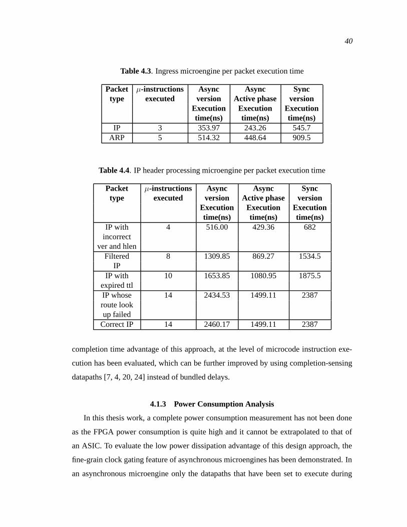
40
Table 4.3. Ingress microengine per packet execution time
Packet µ-instructions Async Async Synctype executed version Active phase version
Execution Execution Executiontime(ns) time(ns) time(ns)
IP 3 353.97 243.26 545.7ARP 5 514.32 448.64 909.5
Table 4.4. IP header processing microengine per packet execution time
Packet µ-instructions Async Async Synctype executed version Active phase version
Execution Execution Executiontime(ns) time(ns) time(ns)
IP with 4 516.00 429.36 682incorrect
ver and hlenFiltered 8 1309.85 869.27 1534.5
IPIP with 10 1653.85 1080.95 1875.5
expired ttlIP whose 14 2434.53 1499.11 2387route lookup failed
Correct IP 14 2460.17 1499.11 2387
completion time advantage of this approach, at the level of microcode instruction exe-
cution has been evaluated, which can be further improved by using completion-sensing
datapaths [7, 4, 20, 24] instead of bundled delays.
4.1.3 Power Consumption Analysis
In this thesis work, a complete power consumption measurement has not been done
as the FPGA power consumption is quite high and it cannot be extrapolated to that of
an ASIC. To evaluate the low power dissipation advantage of this design approach, the
fine-grain clock gating feature of asynchronous microengines has been demonstrated. In
an asynchronous microengine only the datapaths that have been set to execute during

41
a given microinstruction execute. Hence, there is lower power consumption as not all
datapaths execute during each microinstruction execution cycle. Tables 4.5 and 4.6 show
how many datapaths execute in each microinstruction execution cycle for both ingress
and IP-header processing microengines.
4.2 Improving Asynchronous Microengines
The existing implementation of the microengines is not optimized with respect to
performance. The microinstruction is latched only when the ECU is done synchronizing
all datapaths and sufficient time is given for the microinstruction to propagate to the dat-
apaths and set them up along with their RAS blocks. This introduces significant control
overhead of the order of at least 20ns for each microinstruction execution cycle. Also,
the ECU has to wait for the longest datapath thread to finish execution before starting the
next cycle. This introduces significant computational overhead. Methods suggested to
improve the performance of the unoptimized microengine in [12] are summarized below:
Table 4.5. The number of datapaths executing in the IP header processing microengine
microinstruction Number of datapathsexecuting out of total number
1 6/112 1/113 5/114 5/115 5/116 7/117 5/118 4/119 2/11
10 3/1111 3/1112 3/1113 5/1114 4/1115 0/11

42
Table 4.6. The number of datapaths executing in the ingress microengine
microinstruction Number of datapathsexecuting out of total number
1 7/92 2/93 8/94 0/9
• Reducing control overhead: In the four-phase protocol design, the control over-
head can be reduced by latching the next microinstruction with the falling edge
of the global request during the return to zero phase. This allows the setup of
datapaths and RAS blocks when the ECU performs synchronization. This helps
hiding the wasteful return to zero part of a four-phase protocol and can greatly
improve performance.
• Reducing computational overhead: The microengine has to wait for the longest
thread to finish execution before beginning the next execution cycle. These long
latency operations can block the execution of other concurrent thread datapaths
which are done executing earlier. This computational overhead can be consid-
erably reduced by introducing decoupling of datapaths. This technique allows
nondecoupled datapaths to execute the next microinstruction while decoupled-
datapaths are still executing the previous microinstruction. This optimization in-
volves considerable changes to the design of ECU and RAS blocks. An extra
set-decouple microcode field is introduced for each datapath. The ECU no longer
needs to wait for all acknowlegements and will resynchronize with decoupled
datapaths only when it needs to. The circuit-level details have been explained
in [12].
With respect to the FPGA implementation of this architecture, the c-element that
has been used is not optimized. If a c-element with a fan-in of 8 is used instead of
connecting 4 c-elements with fan-in of 2, the synchronization time gets reduced by 7 ns
for each synchronization. This makes the asynchronous version of IP header microengine

43
perform the same as the synchronous version for the longest number of microinstruction
executions. Also, this c-element have been designed as gate-level VHDL description due
to an FPGA implementation instead of fast transistor-level circuit.
4.3 Performance EvaluationMicroengine’s per packet execution time is denoted by the time taken by the external
request’s handshake to complete. The execution time depends from packet to packet.
If any of the IP checks fail, then the microengine will execute fewer microinstructions
and hence, execution time will be reduced. Tables 4.3 and 4.4 show the execution times
for each microengine for all the possible packet cases. For evaluation purposes, we are
considering the total execution time for an ingress microengine for classifying an IP
packet as 353.97 ns and the execution time for IP header processing microengine for
processing an IP packet which gets sent to one of the output ports as 2460.17 ns.
4.3.1 Comparison with Click Software Router
As a starting point, this router’s performance has been compared with a similar Click
software router configuration [18]. Per packet execution times for each of click soft-
ware’s elements running on a 700Mhz Pentium III PC hardware are shown in Table 4.7.
The reason for choosing a Pentium III instead of a gigahertz system for evaluation of this
work is because of the availability of the published numbers in the Click paper [18].
The ingress microengine has implemented Classifier and Paint elements. IP header
processing microengine has implemented Strip, CheckIPheader, GetIPHeader, Lookup-
Table 4.7. Click element’s per packet execution time
Element Time (ns)Classifier 70
Paint 77Strip 67
CheckIPheader 457GetIPaddress 120
LookupIPRoute 140DecIPttl 119

44
IPRoute and DecIPTTL. This evaluation is based on an approximate implementation of
these Click elements as the details such as the number of route table entries in their
element, etc. are not known. Using the execution numbers from the table, it can be
seen that the ingress microengine’s equivalent Click router has a per packet execution
time of 147 ns which is 2.4x better than the ingress microengine. Similarly, IP header
processing microengine’s functionally equivalent click router has a per packet execution
time of 903 ns which is 2.7x better than the microengine implementation. However,
this implementation is an FPGA prototype and that too a SpartanII part which has lower
performance than newer high-performance FPGA parts. Hence. extrapolation of this
FPGA prototype performance results to an ASIC version will give even a more realistic
comparison.
4.3.1.1 Extrapolation of FPGA Results to an ASIC Version
First a 0.5u SCMOS process standard cell library [10] of a generalized asynchronous
microengine control and datapath modules was used for performance comparison against
the SpartanII FPGA modules. A few blocks like ECU, asynchronous RAM, etc. were
implemented on the Xilinx board and their timing was compared with the available stan-
dard cell library. The average execution time speedup that was observed is approximately
5x which factors in the I/O pins delay. This speedup factor is very conservative as
this FPGA to ASIC extrapolation does not take into account the interconnect speedup
that would be much higher than 5. Since the Spartan-II family is designed in a 0.25u,
5LM process technology and the given SCMOS implementation is in a 0.5u process, an
additional speedup of 2x for comparing the two implementations in the same process
technology (0.25u process) was factored in. This assumption of 2x speedup is based
on the constant field scaling model [31] that states that if the feature size of a CMOS
process is scaled down by α, then the gate delay speeds up approximately by α. Thus, the
performance speedup factor for FPGA to ASIC conversion is now 10x. Total per-packet
processing time for a correct IP packet taken by an ASIC version of IP header processing
microengine would roughly be 246.01 ns and that of an ingress microengine would
roughly be 35.39 ns. The asynchronous microengine based router’s performance is 3.9x
45
Click software’s performance that is running on a 700MHz Pentium III (0.18u). The
reason the results from the Click configuration running on a 700Mhz PentiumIII machine
were used instead of using present gigahertz machine was that these were validated and
published results. Although Click’s performance will improve if it runs on a gigahertz
machine, even this design’s performance will scale if it used better process technologies
and design techniques. Assuming a linear scaling factor based on constant field scaling
model, the microengine-based router’s performance is 5.1x Click software’s performance
in the same 0.18u process technology. Since this work has been implemented on a FPGA,
high speed transistor based circuit design techniques were not used. By using better
processes and design techniques for custom CMOS implementation, there is room for a
lot more improvement.
4.3.2 Comparison with Intel’s IXP1200 Network Processor
In this subsection, the per-packet processing time of the extrapolated ASIC version
has been compared with Intel’s IXP1200. This network processor has been chosen for
comparison because its performance evaluation as a router has been done at Princeton
university [27]. Intel 1XP1200 [11] has six RISC cores aka microengines which run
at 200MHz along with a StrongARM core. The data-plane processing is handled by
the microengines whereas the control-plane processing is done by StrongARM. IXP
Microengines are able to do minimal IP forwarding at the rate of 3.47Mpps where each
packet has a size of 64 bytes. The total number of cycles spent in forwarding by a
single microengine including memory access latency adds up to 710 cycles (Each cycle
takes 5ns). The memory latency in the case of IXP gets hidden by multiple contexts
and the system as a whole is able to output a packet every 288ns. This paper [27] has
also mentioned that for doing just IP forwarding, per-packet processing time is 32 cycles
of register instructions which is equivalent to 160ns (32*5ns). However, the authors
have mentioned that their minimal IP forwarder only does ttl decrement, checksum
recompute and ethernet header replacement. The other functions like IP header check
which includes version and checksum check, etc, is done by their classifier. However,
there are no results given for classifier operation. Also, in this thesis the ethernet header

46
replacement has not been implemented. It is very difficult to get an exact performance
number for the tasks that are being performed in the microengine-based router and
comparing those to tasks done by the IXP Microengines. It is still not very clear which
process technology was used for this IXP evaluation. In 1999, the IXP 1200 was based
on 0.28u process and a little later 0.18u process was used. The microengine-based router
(ASIC version 0.18u process) takes 180 ns for doing ttl decrement, checksum check and
recomputation, IP header checks, stateless firewalling and route-lookup. If the ASIC
version of microengine-based router is assumed to be in 0.28u process, the IP header
processing takes 275.5 ns and the packet classification takes 39.63 ns. It seems like in
terms of per-packet performance, this thesis has promising results.
4.4 Throughput Analysis
In the steady state, the maximum throughput of a network device is given by the
processing time of the slowest element. The maximum loss-free throughput of the
microengine-based router(FPGA version) is 406,504 34-byte packets per second whereas
that of the Click router is 333,000 64-byte packets per second. The extrapolated ASIC
version of our implementation would have a throughput of 4,065040 34-byte packets per
second.
CHAPTER 5
CONCLUSIONS AND FUTURE WORK
In this thesis, a case for asynchronous microengines in the network processing do-
main has been presented. This asynchronous microengine-based approach tries to fill
the performance gap between a specialized ASIC and a more general network processor
implementation. It does this by providing a microcoded framework which is close in
performance to ASICs and is also programmable at the finer granularity of microcode.
These asynchronous microengines can be used for designing an asynchronous network
processor architecture which takes advantage of modularity, flexibility, high performance
and low power consumption aspects of an asynchronous design approach.
5.1 Future Work• As part of the future work, completion-sensing can be added to the datapaths. This
would give an average-case performance advantage not just at the microinstruction
level but also at the datapath execution level.
• Another way of increasing this design’s performance would be to implement tech-
niques to reduce the control overhead in the return to zero phase of the four-phase
handshake.
• Implementing an ASIC version would allow doing a more detailed performance
and power measurements.
• It would be interesting to look into microcode generation tools as the present way
of hand coding the binary code is error-prone.
• Measurement of the router’s maximum throughput by working on the assumptions
and simulating the router using real-world network traffic at least in simulation.

APPENDIX A
MICROCODE
A.1 Ingress Microengine Microcode
The microcode for our Ingress Microengine consists of 4 micro-instructions 67 bits
wide. The local control fields corresponding to each datapath and the global control
fields in the microcode have been explained below.
1. Address and Paint Register: This datapath is always the first to execute in any of
the execution chains and has only a set-exe bit associated with it. Microcode for
the address and paint register is shown in Table A.1.
2. 8-bit ALU: This datapath has a set-exe bit, set-seq bit and one of the 8-bits operand
values(offset for the memory address) in the microcode as shown in Table A.2.
3. Offset-address Register: This datapath has been added to prevent the setup time
violation of the packet memory datapath and has a set-seq bit associated with it
as it always executes in sequence with the 8-bit ALU. The microcode is shown in
Table A.3.
4. Packet memory: The packet memory always executes in sequence and does not
need a separate set-exe bit. The microcode for this datapath also has memory
Table A.1. Address register’s microcode
µ-instruction set-exe1 12 03 04 0

49
Table A.2. 8-bit ALU’s microcode
µ-instruction set-exe set-seq 8-bit Operand1 1 1 0x03
2 0 0 0x00
3 1 0 0x04
4 0 0 0x00
Table A.3. Offset register’s microcode
µ-instruction set-exe1 12 03 14 0
related control signals such as the write-enable(we) bit and enable(en) bit. There
is a mux select signal(sel-add) for selecting the address value to be read by the
memory (the value from the address register or the address value after offset has
been added to it). The microcode is shown in Table A.4.
5. Header Register: This datapath has a set-seq bit associated with it and an input
mux signal(sel) for selecting the most significant 16 bits of the packet header or
the least significant 16 bits. The microcode is shown in Table A.5.
6. 16-bit Comparator A: This datapath has a set-seq bit associated with it along with a
16-bit operand value and a 2-bit rule-id field. The microcode is shown in Table A.6.
Table A.4. Packet memory’s microcode
µ-instruction set-seq we en sel-add1 1 0 1 12 0 0 0 03 1 0 1 14 0 0 0 0
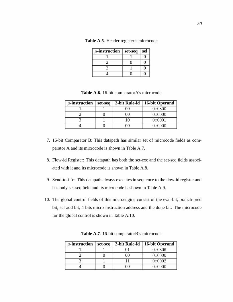
50
Table A.5. Header register’s microcode
µ-instruction set-seq sel1 1 02 0 03 1 04 0 0
Table A.6. 16-bit comparatorA’s microcode
µ-instruction set-seq 2-bit Rule-id 16-bit Operand1 1 00 0x0800
2 0 00 0x0000
3 1 10 0x0001
4 0 00 0x0000
7. 16-bit Comparator B: This datapath has similar set of microcode fields as com-
parator A and its microcode is shown in Table A.7.
8. Flow-id Register: This datapath has both the set-exe and the set-seq fields associ-
ated with it and its microcode is shown in Table A.8.
9. Send-to-fifo: This datapath always executes in sequence to the flow-id register and
has only set-seq field and its microcode is shown in Table A.9.
10. The global control fields of this microengine consist of the eval-bit, branch-pred
bit, sel-add bit, 4-bits micro-instruction address and the done bit. The microcode
for the global control is shown in Table A.10.
Table A.7. 16-bit comparatorB’s microcode
µ-instruction set-seq 2-bit Rule-id 16-bit Operand1 1 01 0x0806
2 0 00 0x0000
3 1 11 0x0002
4 0 00 0x0000

51
Table A.8. Flow-id register’s microcode
µ-instruction set-exe set-seq1 0 02 1 03 1 14 0 0
Table A.9. Send-to-fifo’s microcode
µ-instruction set-seq1 02 13 14 0
Table A.10. Global control microcode
µ-instruction eval branch-pred sel-add 4-bit Operand done1 1 0 0 0x2 02 0 0 1 0x3 03 0 0 0 0x0 04 0 0 1 0x0 1
A.2 IP-Header Processing Microengine
The microcode for our IP-header processing microengine has 15 micro-instructions
that are 111-bits wide. In this microcode, we have not added constant values as operand
fields and have used constant registers instead. This was done so save up on limited
on-chip memory resources. The local control fields corresponding to each datapath and
the global control fields in the microcode have been explained below.
1. Address and Paint Register: This datapath is always the first to execute in any
of the execution chains and thus has only a set-exe bit associated with it and its
microcode is shown in Table A.11.

52
Table A.11. Microcode for IP microengine’s address and paint registers
µ-instruction set-exe1 12 03 04 05 06 07 08 09 0
10 011 012 013 014 015 0
2. 8-bit ALU: This datapath has a set-exe bit, set-seq bit with respect to the address
register, 2-bit opcode, set-mux for selecting one of the inputs and the 8-bits operand
values(offset for the memory address) in the microcode as shown in Table A.12.
3. Packet header store: This datapath consists of set-seq field with respect to the 8-bit
ALU, write enable fields corresponding to the two block RAMs and enable field
(en). The microcode for this datapath is shown in Table A.13.
4. Header Register File: This datapath has been implemented by using 4 dual port
synchronous RAMs and has the widest microcode. The microcode consists of
set-exe, set-seq fields and 4-bit wide read and write port addresses for all the 4
blocks (each block has a byte-wide data in and out port). It also has set-mux fields
for selecting the inputs and outputs. The microcode for the header register file is
shown in Table A.14 and A.15.
5. 16-bit ALU: This datapath has the set-exe field, the set-seq field with respect to
the header register file, a 2-bit and a single bit input set-mux fields as shown in
Table A.16.

53
Table A.12. Microcode of IP microengine’s 8-bit ALU
µ-instruction se ss-add 2-bit opcode sm 8-bit Operand1 1 1 00 0 0x03
2 0 0 00 0 0x00
3 1 0 00 0 0x04
4 1 0 00 0 0x05
5 1 0 00 0 0x06
6 1 0 00 0 0x07
7 1 0 00 0 0x08
8 0 0 00 0 0x00
9 0 0 00 0 0x00
10 1 0 01 1 0x01
11 0 0 00 0 0x00
12 0 0 00 0 0x00
13 1 0 00 0 0x05
14 1 0 00 0 0x06
15 0 0 00 0 0x00
Table A.13. Microcode of IP microengine’s packet store
µ-instruction ss-8bit-ALU we1 we2 en1 1 0 0 12 0 0 0 03 1 0 0 14 1 0 0 15 1 0 0 16 1 0 0 17 1 0 0 18 0 0 0 09 0 0 0 010 0 0 0 011 0 0 0 012 0 0 0 013 1 0 1 114 1 1 0 115 0 0 0 0

54
Table A.14. Microcode of IP microengine’s header register file
µ se ss ss we(1:4) wr wr wr wrinsn packet tempreg add-b1 add-b2 add-b3 add-b4
1 1 1 0 0xC 0x0 0x0 0x0 0x0
2 0 0 0 0x0 0x0 0x0 0x0 0x0
3 1 1 0 0xF 0x1 0x1 0x0 0x0
4 1 1 0 0xF 0x2 0x2 0x1 0x1
5 1 1 0 0xF 0x3 0x3 0x2 0x2
6 1 1 0 0xF 0x4 0x4 0x3 0x3
7 1 1 0 0x3 0x0 0x0 0x4 0x4
8 0 0 0 0x0 0x0 0x0 0x0 0x0
9 0 0 0 0x0 0x0 0x0 0x0 0x0
10 0 0 0 0x0 0x0 0x0 0x0 0x0
11 0 0 0 0x0 0x0 0x0 0x0 0x0
12 1 0 0 0x8 0x2 0x0 0x0 0x0
13 1 0 1 0x3 0x0 0x0 0x2 0x2
14 0 0 0 0x0 0x0 0x0 0x0 0x0
15 0 0 0 0x0 0x0 0x0 0x0 0x0
6. 16-bit Comparator: This datapath has set-mux fields for input operands, a 2-bit
opcode, set-exe and set-seq field with respect to the header register file and its
microcode is shown in Table A.17.
7. 16-bit temporary registers: This datapath has two temporary registers(A and B)
and each of them have a separate enable field and they share the set-seq field and
its microcode is shown in Table A.18.
8. Route Look-up CAM, Filter CAM and Send-to-Fifo: These CAMs have the set-exe
field each. The lookup CAM has additional fields: write enable(we) and enable(en)
for the look-up route table Block RAM. The Send-to-fifo datapath has the set-exe
field and the set-seq field with respect to flow-id register datapath. The microcode
for these datapaths has been shown in Table A.19.

55
Table A.15. Microcode of IP microengine’s header register file contd.
µ sm-in1 sm-in2 sm-in3 read read read read sm-outinsn add-b1 add-b2 add-b3 add-b4 1 to 4
1 0 0 0 0x0 0x0 0x0 0x0 0xF
2 0 0 0 0x0 0x0 0x0 0x0 0x0
3 0 0 0 0x0 0x0 0x0 0x0 0x3
4 0 0 0 0x1 0x1 0x0 0x0 0x0
5 0 0 0 0x0 0x0 0x1 0x1 0x0
6 0 0 0 0x3 0x3 0x0 0x0 0x0
7 0 0 0 0x0 0x0 0x3 0x3 0x0
8 0 0 0 0x2 0x0 0x4 0x4 0x0
9 0 0 0 0x4 0x4 0x0 0x0 0x0
10 0 0 0 0x2 0x2 0x0 0x0 0x0
11 0 0 0 0x4 0x0 0x2 0x2 0x0
12 1 0 0 0x0 0x0 0x0 0x0 0x0
13 0 1 1 0x2 0x2 0x0 0x0 0x0
14 0 0 0 0x0 0x0 0x2 0x2 0x0
15 0 0 0 0x0 0x0 0x0 0x0 0x0
Table A.16. Microcode of IP microengine’s 16-bit ALU
µ-instruction se ss-header 2-bit sm-in1 sm-in21 0 0 00 02 0 0 00 03 1 1 00 14 1 0 10 05 1 0 10 16 1 0 10 07 1 0 10 18 1 0 10 19 1 0 10 0
10 1 0 10 011 1 0 10 112 0 0 00 013 1 0 11 014 0 0 00 015 0 0 00 0

56
Table A.17. Microcode of IP microengine’s 16-bit comparator
µ- se ss- 3-bit 3-bit 2-bit sm-in4 2-bitinstruction header sm-in1 sm-in2 sm-in3 opcode
1 1 1 100 000 11 0 012 0 0 000 000 00 0 003 0 0 000 000 00 0 004 0 0 000 000 00 0 005 0 0 000 000 00 0 006 0 0 000 000 00 0 007 0 0 000 000 00 0 008 1 0 100 000 00 0 109 0 0 000 000 00 0 00
10 0 0 000 000 00 0 0011 0 0 000 000 00 0 0012 1 0 101 100 10 1 0013 0 0 000 000 00 0 0014 0 0 000 000 00 0 0015 0 0 000 000 00 0 00
Table A.18. Microcode of IP microengine’s 16-bit temporary registers
µ-instruction ss-16bitALU enA enB1 0 0 02 0 0 03 1 1 04 1 1 05 1 1 06 1 1 07 1 1 08 1 1 09 1 1 1
10 1 1 011 1 1 012 0 0 013 1 1 014 0 0 015 0 0 0
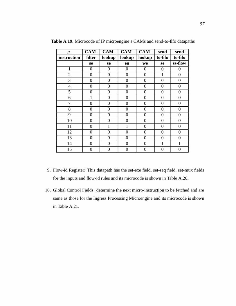
57
Table A.19. Microcode of IP microengine’s CAMs and send-to-fifo datapaths
µ- CAM- CAM- CAM- CAM- send sendinstruction filter lookup lookup lookup to-fifo to-fifo
se se en we se ss-flow1 0 0 0 0 0 02 0 0 0 0 1 03 0 0 0 0 0 04 0 0 0 0 0 05 0 0 0 0 0 06 1 0 0 0 0 07 0 0 0 0 0 08 0 0 0 0 0 09 0 0 0 0 0 0
10 0 0 0 0 0 011 0 1 1 0 0 012 0 0 0 0 0 013 0 0 0 0 0 014 0 0 0 0 1 115 0 0 0 0 0 0
9. Flow-id Register: This datapath has the set-exe field, set-seq field, set-mux fields
for the inputs and flow-id rules and its microcode is shown in Table A.20.
10. Global Control Fields: determine the next micro-instruction to be fetched and are
same as those for the Ingress Processing Microengine and its microcode is shown
in Table A.21.
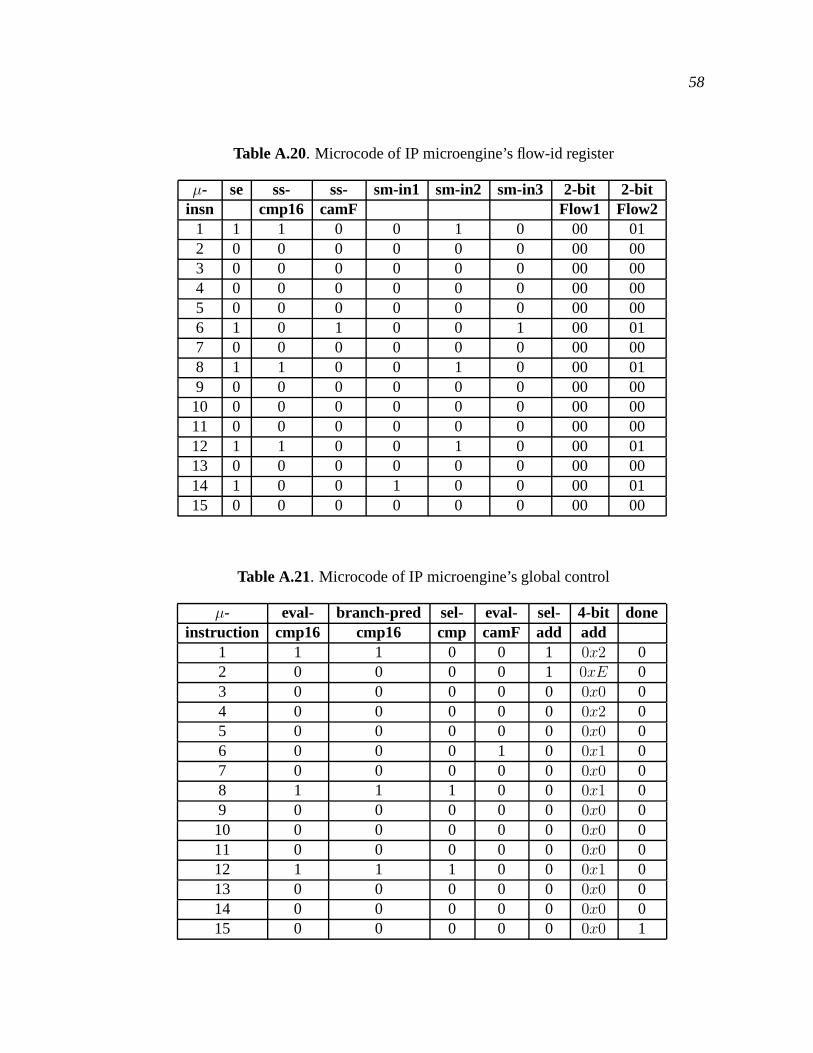
58
Table A.20. Microcode of IP microengine’s flow-id register
µ- se ss- ss- sm-in1 sm-in2 sm-in3 2-bit 2-bitinsn cmp16 camF Flow1 Flow2
1 1 1 0 0 1 0 00 012 0 0 0 0 0 0 00 003 0 0 0 0 0 0 00 004 0 0 0 0 0 0 00 005 0 0 0 0 0 0 00 006 1 0 1 0 0 1 00 017 0 0 0 0 0 0 00 008 1 1 0 0 1 0 00 019 0 0 0 0 0 0 00 00
10 0 0 0 0 0 0 00 0011 0 0 0 0 0 0 00 0012 1 1 0 0 1 0 00 0113 0 0 0 0 0 0 00 0014 1 0 0 1 0 0 00 0115 0 0 0 0 0 0 00 00
Table A.21. Microcode of IP microengine’s global control
µ- eval- branch-pred sel- eval- sel- 4-bit doneinstruction cmp16 cmp16 cmp camF add add
1 1 1 0 0 1 0x2 02 0 0 0 0 1 0xE 03 0 0 0 0 0 0x0 04 0 0 0 0 0 0x2 05 0 0 0 0 0 0x0 06 0 0 0 1 0 0x1 07 0 0 0 0 0 0x0 08 1 1 1 0 0 0x1 09 0 0 0 0 0 0x0 0
10 0 0 0 0 0 0x0 011 0 0 0 0 0 0x0 012 1 1 1 0 0 0x1 013 0 0 0 0 0 0x0 014 0 0 0 0 0 0x0 015 0 0 0 0 0 0x0 1

APPENDIX B
SOURCE CODE
library IEEE;use IEEE.std_logic_1164.all;use IEEE.std_logic_signed.all;use IEEE.std_logic_arith.all;
entity celement isport (clear, a, b : in STD_LOGIC;
c : inout STD_LOGIC);end celement;
architecture behv of celement isbegin
process (clear,c,a,b)begin -- process clr
if clear = ’1’ thenc <= ’0’;
elsif a = ’1’ and b = ’1’ thenc <= ’1’;elsif a = ’0’ and b = ’0’ then
c <= ’0’;
else c <= c;
end if;end process ;
end behv;
Figure B.1. Source code of a 2-input c-element

60
library IEEE;use IEEE.std_logic_1164.all;
entity BDU is
port (eval_camf, eval_cmp16, matchf : in std_logic;
cmp16_out, braped_cmp16 : in std_logic;clear : out std_logic);
end BDU;
architecture behv of BDU issignal branch : std_logic;begin
branch <= (eval_camf and matchf) or(eval_cmp16 and cmp16_out);clear <= branch xor braped_cmp16;
end behv;
Figure B.2. Source code of IP-header processing microengine’s BDU

61
library IEEE;use IEEE.std_logic_1164.all;use IEEE.std_logic_arith.all;use IEEE.std_logic_unsigned.all;
entity next_add isport (req,sel_addr,extack, clear, reset : in std_logic;branch_addr : in std_logic_vector(3 downto 0);--inc_addr_reg : inout std_logic_vector(3 downto 0);next_addr : out std_logic_vector(3 downto 0));
end next_add;architecture behv of next_add issignal int_nxt_addr,inc_addr,inc_addr_reg
: std_logic_vector(3 downto 0);
begin -- behvprocess (int_nxt_addr)begin -- processinc_addr <= int_nxt_addr +1;
end process;
process (inc_addr,clear,req, extack)begin -- processif (extack = ’1’) then
inc_addr_reg <= "0000";elseif (req’event and (req = ’1’)) then
if (clear = ’0’) theninc_addr_reg <= inc_addr;
end if;end if;
end if;end process;
process (inc_addr_reg,branch_addr,sel_addr)begin -- process
if (sel_addr = ’0’) thenint_nxt_addr <= inc_addr_reg;
elseint_nxt_addr <= branch_addr;
end if;end process;
Figure B.3. Source code of next-address logic
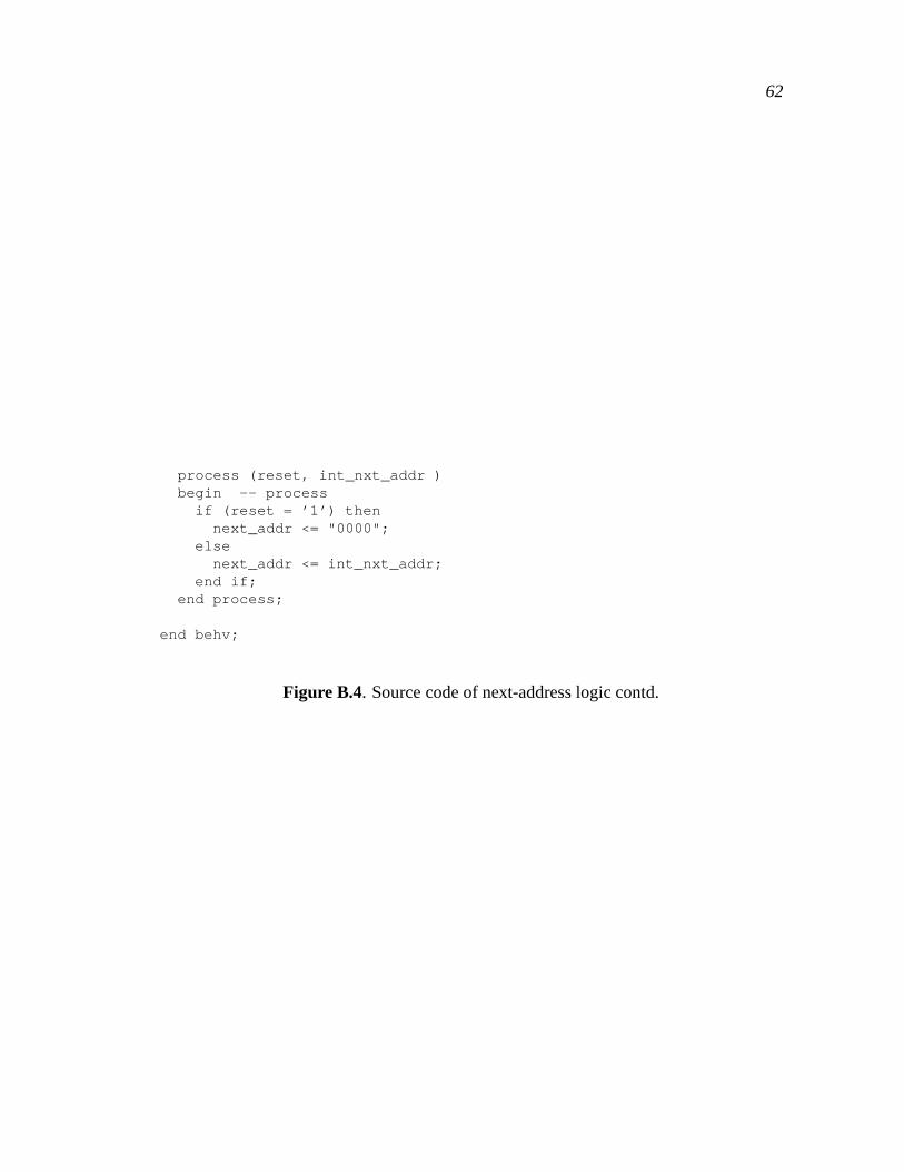
62
process (reset, int_nxt_addr )begin -- processif (reset = ’1’) then
next_addr <= "0000";else
next_addr <= int_nxt_addr;end if;
end process;
end behv;
Figure B.4. Source code of next-address logic contd.

63
library IEEE;use IEEE.std_logic_1164.all;use IEEE.std_logic_arith.all;
entity mi_reg is
port (a : in std_logic_vector(110 downto 0);req,clear,sel_addr : in std_logic;reset : in std_logic;
q : inout std_logic_vector(110 downto 0));
end mi_reg;
architecture rtl of mi_reg isbeginprocess (reset, req)beginif reset = ’1’ then
q <= "00000000000000000000000000000000000000000000000000
0000000000000000000000000000000000000000000000000000000000000";else
if rising_edge(req) thenif clear = ’1’ then
q(110 downto 6) <= "000000000000000000000000000000000000000000000000000000000000000000000000000000000000000000000000
000000000";q(5) <= sel_addr;q(4 downto 1) <= q(4 downto 1);q(0) <= ’0’;
elseq <= a;
end if;
end if;
end if;end process;
end rtl;
Figure B.5. Source code of IP-header processing microengine’s microinstruction register
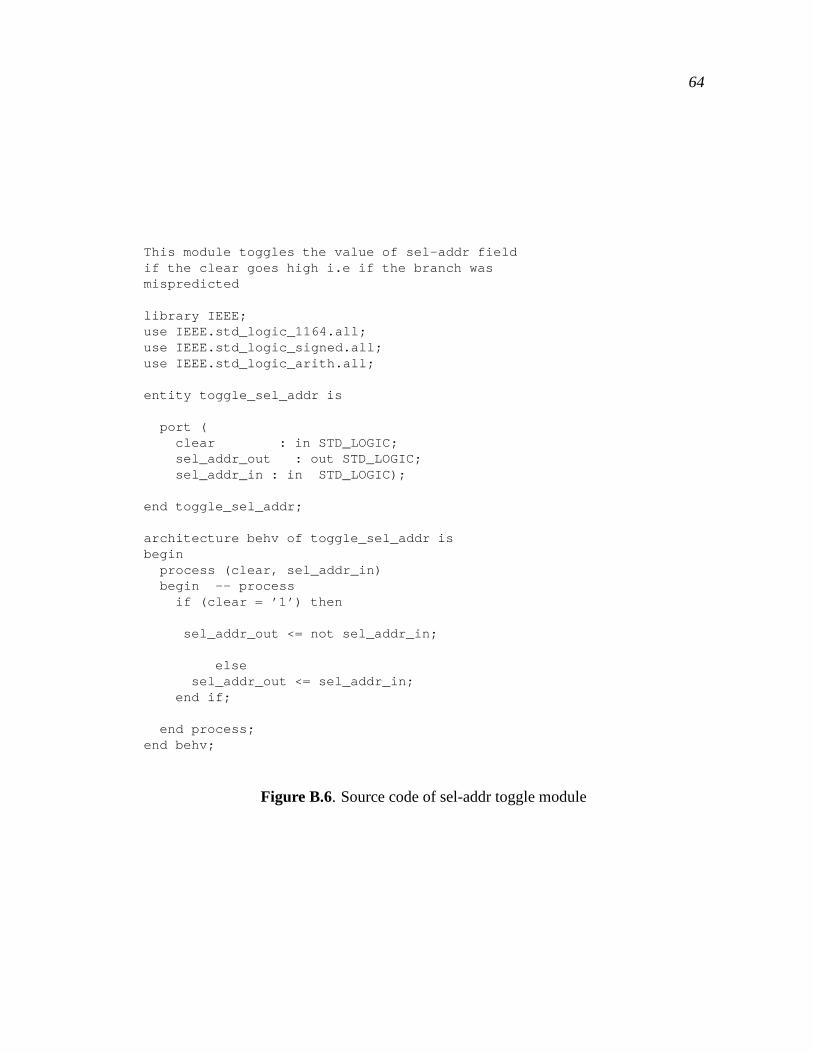
64
This module toggles the value of sel-addr fieldif the clear goes high i.e if the branch wasmispredicted
library IEEE;use IEEE.std_logic_1164.all;use IEEE.std_logic_signed.all;use IEEE.std_logic_arith.all;
entity toggle_sel_addr is
port (clear : in STD_LOGIC;sel_addr_out : out STD_LOGIC;sel_addr_in : in STD_LOGIC);
end toggle_sel_addr;
architecture behv of toggle_sel_addr isbegin
process (clear, sel_addr_in)begin -- processif (clear = ’1’) then
sel_addr_out <= not sel_addr_in;
elsesel_addr_out <= sel_addr_in;
end if;
end process;end behv;
Figure B.6. Source code of sel-addr toggle module
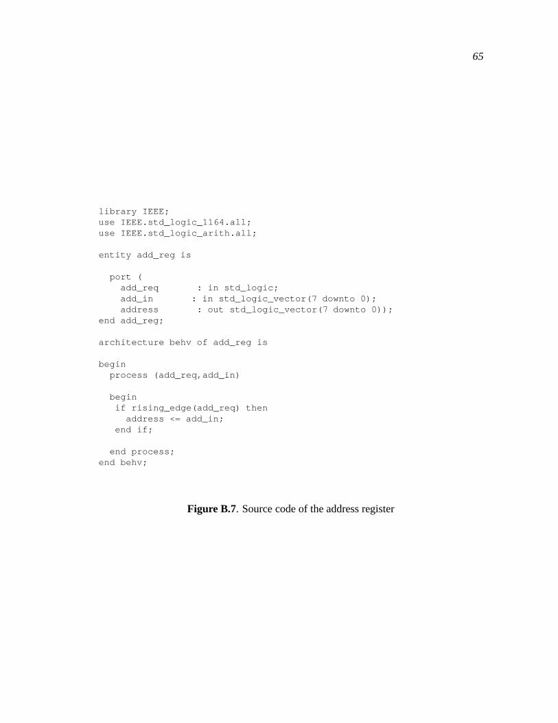
65
library IEEE;use IEEE.std_logic_1164.all;use IEEE.std_logic_arith.all;
entity add_reg is
port (add_req : in std_logic;add_in : in std_logic_vector(7 downto 0);address : out std_logic_vector(7 downto 0));
end add_reg;
architecture behv of add_reg is
beginprocess (add_req,add_in)
beginif rising_edge(add_req) then
address <= add_in;end if;
end process;end behv;
Figure B.7. Source code of the address register
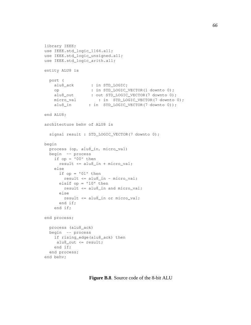
66
library IEEE;use IEEE.std_logic_1164.all;use IEEE.std_logic_unsigned.all;use IEEE.std_logic_arith.all;
entity ALU8 is
port (alu8_ack : in STD_LOGIC;op : in STD_LOGIC_VECTOR(1 downto 0);alu8_out : out STD_LOGIC_VECTOR(7 downto 0);micro_val : in STD_LOGIC_VECTOR(7 downto 0);alu8_in : in STD_LOGIC_VECTOR(7 downto 0));
end ALU8;
architecture behv of ALU8 is
signal result : STD_LOGIC_VECTOR(7 downto 0);
beginprocess (op, alu8_in, micro_val)begin -- processif op = "00" then
result <= alu8_in + micro_val;else
if op = "01" thenresult <= alu8_in - micro_val;
elsif op = "10" thenresult <= alu8_in and micro_val;
elseresult <= alu8_in or micro_val;
end if;end if;
end process;
process (alu8_ack)begin -- processif rising_edge(alu8_ack) thenalu8_out <= result;
end if;end process;
end behv;
Figure B.8. Source code of the 8-bit ALU

67
library IEEE;use IEEE.std_logic_1164.all;use IEEE.std_logic_unsigned.all;use IEEE.std_logic_arith.all;
entity ALU16 is
port (alu16_ack : in STD_LOGIC;
alu16_out : out STD_LOGIC_VECTOR(15 downto 0);ain : in STD_LOGIC_VECTOR(15 downto 0);bin : in STD_LOGIC_VECTOR(15 downto 0));
end ALU16;
architecture behv of ALU16 is
signal result : STD_LOGIC_VECTOR(15 downto 0);
beginprocess (ain, bin)begin -- process
result <= ain + bin;end process;
process (alu16_ack)begin -- processif rising_edge(alu16_ack) thenalu16_out <= result;
end if;end process;
end behv;
Figure B.9. Source code of the 16-bit ALU
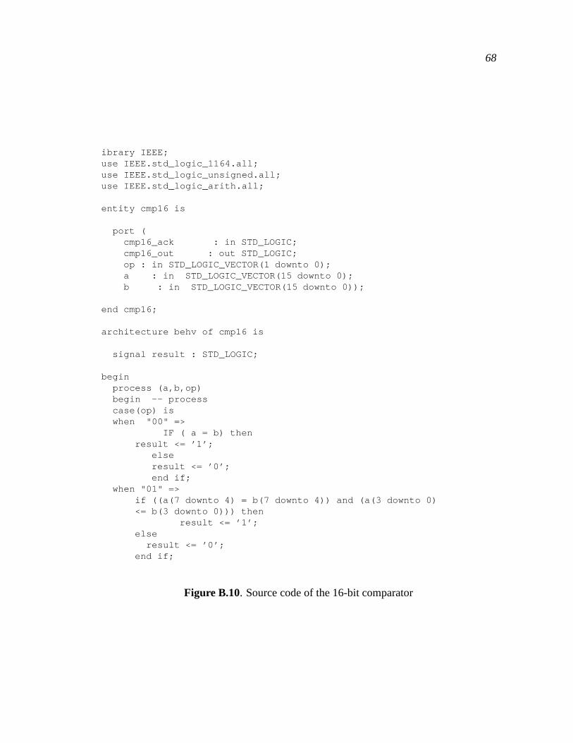
68
ibrary IEEE;use IEEE.std_logic_1164.all;use IEEE.std_logic_unsigned.all;use IEEE.std_logic_arith.all;
entity cmp16 is
port (cmp16_ack : in STD_LOGIC;cmp16_out : out STD_LOGIC;op : in STD_LOGIC_VECTOR(1 downto 0);a : in STD_LOGIC_VECTOR(15 downto 0);b : in STD_LOGIC_VECTOR(15 downto 0));
end cmp16;
architecture behv of cmp16 is
signal result : STD_LOGIC;
beginprocess (a,b,op)begin -- processcase(op) iswhen "00" =>
IF ( a = b) thenresult <= ’1’;
elseresult <= ’0’;end if;
when "01" =>if ((a(7 downto 4) = b(7 downto 4)) and (a(3 downto 0)<= b(3 downto 0))) then
result <= ’1’;else
result <= ’0’;end if;
Figure B.10. Source code of the 16-bit comparator

69
when "10" =>if (a > b) then
result <= ’1’;else
result <= ’0’;end if;
when others =>result <= ’0’;
end case;
end process;
process (cmp16_ack)begin -- processif rising_edge(cmp16_ack) thencmp16_out <= result;
end if;end process;
end behv;
Figure B.11. Source code of the 16-bit comparator contd
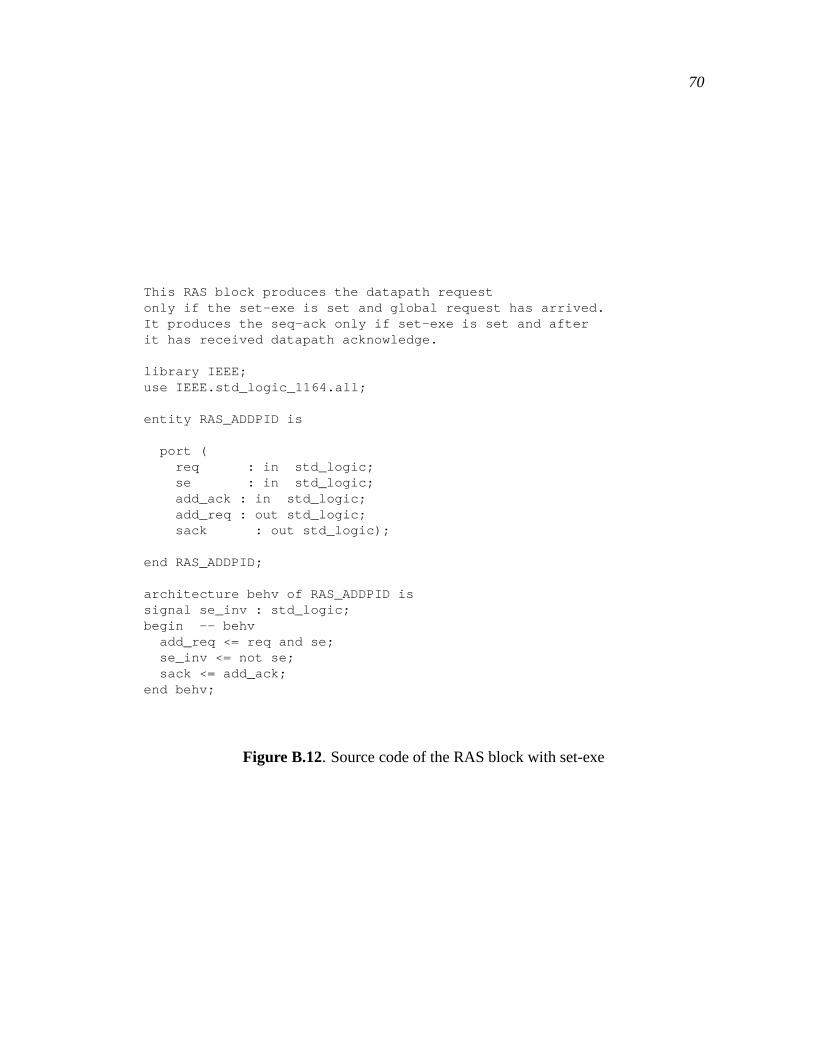
70
This RAS block produces the datapath requestonly if the set-exe is set and global request has arrived.It produces the seq-ack only if set-exe is set and afterit has received datapath acknowledge.
library IEEE;use IEEE.std_logic_1164.all;
entity RAS_ADDPID is
port (req : in std_logic;se : in std_logic;add_ack : in std_logic;add_req : out std_logic;sack : out std_logic);
end RAS_ADDPID;
architecture behv of RAS_ADDPID issignal se_inv : std_logic;begin -- behv
add_req <= req and se;se_inv <= not se;sack <= add_ack;
end behv;
Figure B.12. Source code of the RAS block with set-exe

71
This RAS block produces the datapath request uponthe following conditions:a) set-exe is set and global request has arrivedb) if set-seq is set then it needs to wait for seq-reqto arrive tooIt produces the seq-ack only whenset-exe is set and it has received datapath ack.It produces the Ack signal whena) if set-exe is set then it waits for datapath ackb) if set-exe is not set then it produces the Ack afterglobal req arrives.
library IEEE;use IEEE.std_logic_1164.all;
entity ras_alu8 is
port (req : in std_logic;se : in std_logic;alu8_ack : in std_logic;alu8_req : out std_logic;sack_alu8 : out std_logic;ss_add : in std_logic;sack_add : in std_logic;ack1 : out std_logic);
end ras_alu8;
architecture behv of ras_alu8 issignal se_inv, ss_add_inv : std_logic;begin -- behv
ss_add_inv <= not ss_add ;alu8_req <= (req and se and (ss_add_inv or sack_add));se_inv <= not se;sack_alu8 <= alu8_ack;ack1 <= (se_inv and req) or alu8_ack;
end behv;
Figure B.13. Source code of the RAS block with set-exe and set-seq

72
This RAS block generates the datapath reqwhen its set-seq bit is set and it has receivedthe seq-req and the global request.It generates the seq-ack only when set-seq is set andit has received the datapath ack.It generates the Ack only when set-seq is set andit has received the datapath ack or if set-seq is notset then upon arrival of global req.
library IEEE;use IEEE.std_logic_1164.all;
entity ras_packet is
port (ss_alu8 , sreq_alu8, req, packet_ack : in std_logic;ack2, packet_req ,sack_packet: out std_logic);
end ras_packet;
architecture behv of ras_packet issignal ss_inv : std_logic;
begin -- behvss_inv <= not ss_alu8;packet_req <= (ss_alu8 and sreq_alu8 and req);ack2 <= ((ss_inv and req) or packet_ack);sack_packet <= packet_ack;
end behv;
Figure B.14. Source code of the RAS block with set-seq

73
This RAS block is similar to the one with a single set-seqbit and set-exe except for that it needs to wait for seq-reqcorresponding to the set-seq bit.
library IEEE;use IEEE.std_logic_1164.all;
entity ras_flow is
port (ss_cmp16, ss_camf, se, sreq_cmp16,sreq_camf, req, flow_ack : in std_logic;ack6, flow_req , sack_flow: out std_logic);
end ras_flow;
architecture behv of ras_flow issignal se_inv, ss_camf_inv, ss_cmp16_inv : std_logic;
begin -- behvse_inv <= not se;ss_camf_inv <= not ss_camf;ss_cmp16_inv <= not ss_cmp16;flow_req <= ((ss_camf_inv or sreq_camf) and
(ss_cmp16_inv or sreq_cmp16) and se and req);ack6 <= ((se_inv and req) or flow_ack);sack_flow <= flow_ack;
end behv;
Figure B.15. Source code of the RAS block with multiple set-seq bits and set-exe

REFERENCES
[1] G. A. Andreas Nowatzyk and F. Pong. Design of the S3MP processor. In Proc. ofEuropar Workshop, 1995.
[2] C. V. Berkel, M. Josephs, and S. Nowick. Scanning the technology- applicationsof asynchronous circuits. In Proc. of IEEE, volume 87, pages 234–242, February1999.
[3] E. Brunvand. Translating Concurrent Communicating Programs into Asyn-chronous Circuits. PhD thesis, Carnegie Mellon University, 1991.
[4] F. C. Cheng, S. H. Unger, and M. Theobald. Self-timed Carry-lookahead Adders.IEEE Transactions on Computers, 49(7):659–672, 2000.
[5] D. E. Comer. Network Systems Design using Network Processors. Prentice Hall,2003.
[6] A. Davis and S. M. Nowick. An introduction to asynchronous circuit design.Technical Report UUCS-97-013, School of Computing, University of Utah, Sept.1997.
[7] J. Escriba and J. A. Carrasco. Self-timed Manchester Chain Carry Propagate Adder.Electronic Letters, 32(8):708–710, 1996.
[8] C. P. et al. A 50-Gb/s ip router. IEEE/ACM Transactions on Networking, 6(3), June1998.
[9] S. B. Furber, J. D. Garside, and S. Temple. Power-saving features in Amulet2e. InIn Proc. of Power Driven Microarchitecture Workshop, June 1998.
[10] G. Gulati and E. Brunvand. Design of a cell library for asynchronous microengines.In Proc. of Great Lakes VLSI, 2005.
[11] Intel IXP12XX product line of network processors. http://www.intel.com/design/network/products/npfamily/ixp1200.htm.
[12] H. Jacobson and G. Gopalakrishnan. Application-specific asynchronous micro-engines for efficient high-level control. Technical Report UUCS-97-007, School ofComputing, University of Utah, 1997.
[13] H. Jacobson and G. Gopalakrishnan. Asynchronous microengines for high-levelcontrol. In Proc. of 17th Conf. on Advanced Research in VLSI(ARVLSI97), 1997.
75
[14] H. Jacobson and G. Gopalakrishnan. Application-specific programmable controlfor high-performance asynchronous circuits. In Proc. of IEEE in a special asyn-chronous issue, volume 92, February 1999.
[15] S. Keshav. An Engineering Approach to Computer Networking. Addison Wesley,1999.
[16] S. Keshav and R. Sharma. Issues and trends in router design. IEEE Communica-tions Magazine, 36(5):144–151, May 1998.
[17] E. Kohler. The Click Modular Router. PhD thesis, Dept. of Computer Science,MIT, 2000.
[18] E. Kohler, R. Morris, B. Chen, J. Jannotti, and M. F. Kaashoek. The click modularrouter. ACM Transactions on Computer Systems, 18(3):263–297, August 2000.
[19] J. Kuskin and D. O. et al. The stanford FLASH multiprocessor. In Proc. of 21stAnnual International Symposium on Computer Architecture, pages 302–313, 1994.
[20] A. J. Martin. Asynchronous Datapaths and the Design of an Asynchronous Adder.Formal Methods in System Design, 1(1):119–137, July 1992.
[21] C. Myers. Asynchronous Circuit Design. Wiley, 2001.
[22] L. Peterson and B. Davie. Computer Networks- A system’s approach. MorganKaufmann, 1999.
[23] P. A. Riocreux, L. E. M. Brackenbury, M. Cumpstey, and S. B. Furber. A Low-Power Self-Timed Viterbi Decoder. In In Proc. of ASYNC, pages 15–24, March2001.
[24] O. Salomon and H. Klar. Self-timed fully pipelined multipliers. In IFIP Transac-tions : Computer Science and Technology, volume A-28, pages 45–55, 1993.
[25] C. Seitz. Chapter 7 ”System Timing” Introduction to VLSI Systems(Mead andConway). Addison Wesley, 1980.
[26] N. Shah. Understanding Network Processors. Master’s thesis, Dept. of EECS,University of California, Berkeley, September 2001.
[27] T. Spalink, S. Karlin, L. Peterson, and Y. Gottlieb. Building a Robust Software-Based Router Using Network Processors. In Proc. of the 18th ACM Symposiumon Operating Systems Principles (SOSP), pages 216–229, Chateau Lake Louise,Banff, Alberta, Canada, October 2001.
[28] K. Stevens. The soft-controller: A self-timed microsequencer for distributedparallel architectures. Technical report, School of Computing, University of Utah,1984.
[29] W. R. Stevens. The Protocols(TCP/IP Illustrated Volume 1). Addison-Wesley,1994.

76
[30] I. E. Sutherland. Micropipelines. Communications of the ACM, 32(6):720–738,June 1989.
[31] N. Weste and D. Harris. Principles of CMOS VLSI Design: A System’s Perspective(3rd Edition). Addison-Wesley, 2005.
[32] Xilinx 2.5V Spartan II FPGA Family: Complete Datasheet. http://direct.xilinx.com/bvdocs/publications/ds001.pdf/.
[33] Xilinx Application Note:An Overview of Multiple CAM Designs in Virtex FamilyDevices. http://xilinx.com/bvdocs/appnotes/xapp201.pdf.
[34] K. Y. Yun. Synthesis of Asynchronous Controllers for Heterogenous Systems. PhDthesis, Stanford University, 1994.