assignment of tasks „hw for ultrasonic distance meter“ - …€¦ · · 2011-02-13assignment...
TRANSCRIPT
Assignment of tasks „HW for ultrasonic distance meter“
Abstract The ultrasonic distance meter project takes place in the fourth semester of the electrical engineering curriculum at the Zurich University of Applied Sciences.
Students build a distance meter from scratch, developing and implementing the required hardware and software. Furthermore the students can refine their algorithms to challenge and improve the performance of their own device.
This document focuses on the hardware concept.
The students have to outline different solution possibilities with their advantages and drawbacks, decide on the most advantageous design, develop the circuit, do calculations and simulations, route the printed circuit board, assemble and solder the board, test the circuit and compare the results with the specifications and document the whole process of hardware development in an intermediate report in English.
Given the short available time, this paper addresses some special issues and suggests solution possibilities to speed up the implementation procedure.
The original URL of this paper is http://www.zhaw.ch/~hhrt/ETP/assignment_HW_design.pdf
All the other documents mentioned in this paper such as datasheets, TINA simulations, the EAGLE library for the printed circuit board layout of special components, the description of the microcontroller board and the evaluation checklist are packed in this archive: http://www.zhaw.ch/~hhrt/ETP/ETP_HW.zip
© Hanspeter Hochreutener, [email protected] , 13. February 2011
Centre for Signal Processing and Communications Engineering, http://zsn.zhaw.ch
School of Engineering http://www.engineering.zhaw.ch/
Zurich University of Applied Sciences http://www.zhaw.ch
assignment_HW_design.doc Seite 1 / 16 H. Hochreutener, SoE@ZHAW

Table of contents
1. Introduction ........................................................................................................................... 3 2. Specification.......................................................................................................................... 3 3. Transducer ............................................................................................................................ 4
3.1. Link budget calculation and signal levels...................................................................... 5 4. Sender................................................................................................................................... 6
4.1. Schematic of the circuit and simulated signals ............................................................. 6 4.2. Transformer .................................................................................................................. 8 4.3. Power transistors .......................................................................................................... 8 4.4. Printed circuit board layout with ground plate............................................................... 9
5. Receiver .............................................................................................................................. 10 5.1. Gain control ................................................................................................................ 10 5.2. Operational amplifier .................................................................................................. 11 5.3. Input over-voltage protection ...................................................................................... 12 5.4. Anti aliasing filter ........................................................................................................ 12 5.5. Printed Circuit board layout with star-type grounding ................................................. 12
6. Temperature compensation of the speed of sound............................................................. 13 7. Testing ................................................................................................................................ 14 8. Appendix ............................................................................................................................. 15
8.1. PCB-SW EAGLE: design rules, ground and symbols................................................. 15 8.1.1. Design rules........................................................................................................ 15 8.1.2. Ground plate (digital): property settings for the GND-polygon............................ 15 8.1.3. Star-type grounding for analog circuitry: how to proceed ................................... 15 8.1.4. Ground connections: digital - supply - analog..................................................... 16
8.2. Related documents: datasheets, simulations, footprints ............................................ 16 8.3. Table of contents for the intermediate report.............................................................. 16
assignment_HW_design.doc Seite 2 / 16 H. Hochreutener, SoE@ZHAW
1. Introduction The distance meter uses an ultrasonic transducer, which is a device that converts electrical signals in ultrasonic waves and vice versa.
The simplest way to measure a distance using an ultrasonic transducer is to send a pulse packet, wait for the echo and measure the elapsed time. As the speed of sound is known to be 343m/s in dry air of 20°C, the distance can easily be calculated from the roundtrip delay = time of flight (TOF). If you want to know more about ultrasound, visit http://en.wikipedia.org/wiki/Ultrasonic_sensor
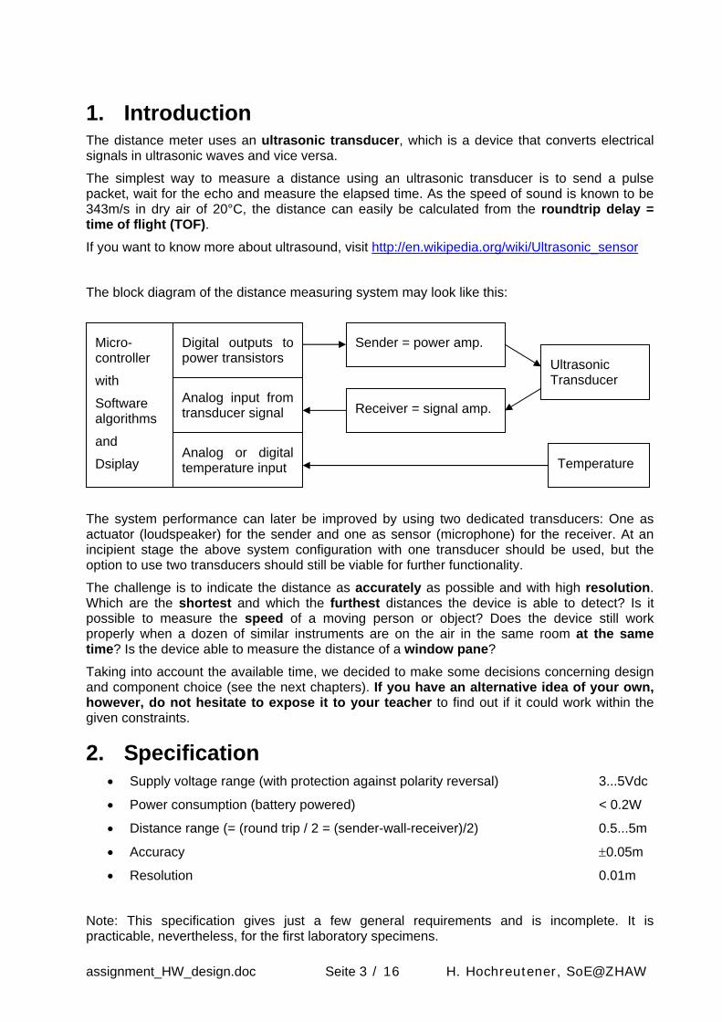
The block diagram of the distance measuring system may look like this:
Digital outputs to power transistors
Analog input from transducer signal
Sender = power amp.
Receiver = signal amp.
Ultrasonic Transducer
Analog or digital temperature input Temperature
Micro- controller
with
Software algorithms
and
Dsiplay
The system performance can later be improved by using two dedicated transducers: One as actuator (loudspeaker) for the sender and one as sensor (microphone) for the receiver. At an incipient stage the above system configuration with one transducer should be used, but the option to use two transducers should still be viable for further functionality.
The challenge is to indicate the distance as accurately as possible and with high resolution. Which are the shortest and which the furthest distances the device is able to detect? Is it possible to measure the speed of a moving person or object? Does the device still work properly when a dozen of similar instruments are on the air in the same room at the same time? Is the device able to measure the distance of a window pane?
Taking into account the available time, we decided to make some decisions concerning design and component choice (see the next chapters). If you have an alternative idea of your own, however, do not hesitate to expose it to your teacher to find out if it could work within the given constraints.
2. Specification • Supply voltage range (with protection against polarity reversal) 3...5Vdc
• Power consumption (battery powered) < 0.2W
• Distance range (= (round trip / 2 = (sender-wall-receiver)/2) 0.5...5m
• Accuracy ±0.05m
• Resolution 0.01m
Note: This specification gives just a few general requirements and is incomplete. It is practicable, nevertheless, for the first laboratory specimens.
assignment_HW_design.doc Seite 3 / 16 H. Hochreutener, SoE@ZHAW
3. Transducer We decided on using the cheap ultrasonic transducer 400PT160 (CHF 10.-) which can be used as “loudspeaker” and/or as “microphone”.
The datasheet of this transducer (and all other important files for the hardware) is in the archive mentioned on the first page of this paper.
The main characteristics of this transducer are discussed below.
The centre frequency of 40kHz is well above the audible limit of 20kHz and still low enough that there are no special requirements to the analog circuitry. The Nyquist criterion asks for a minimal sampling frequency of the analog to digital converter of 80kHz. In practice the sampling frequency should be at least 120kHz.
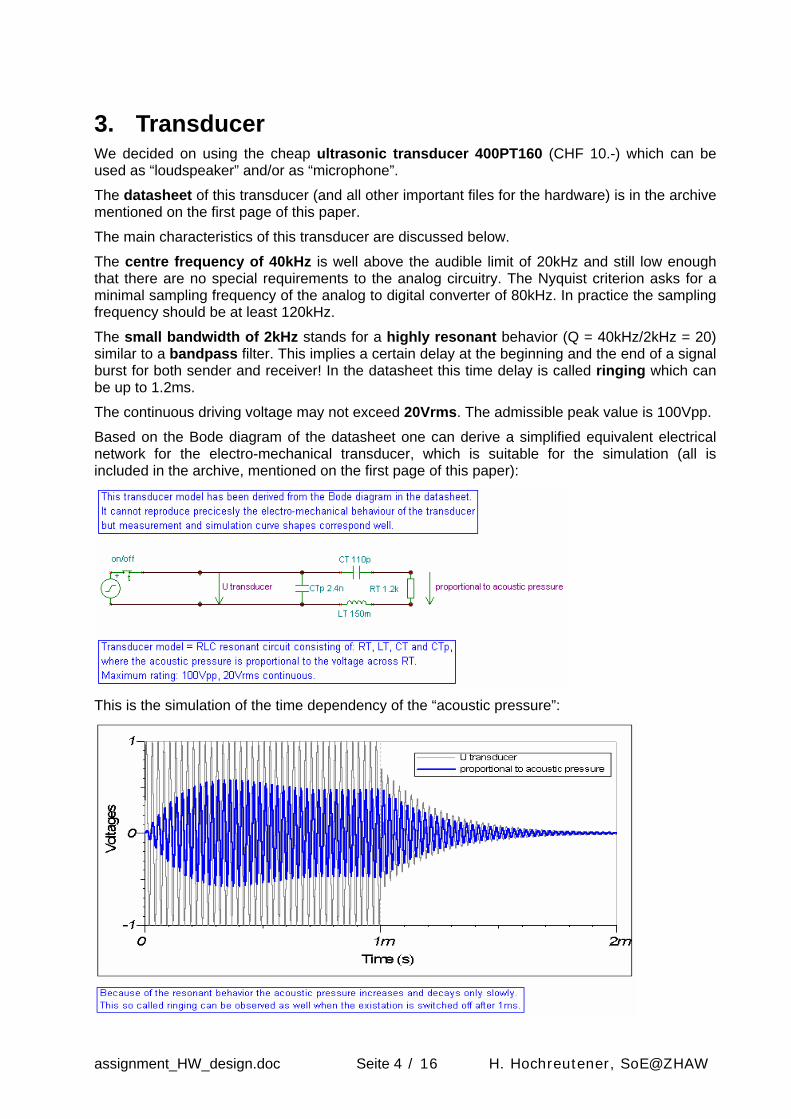
The small bandwidth of 2kHz stands for a highly resonant behavior (Q = 40kHz/2kHz = 20) similar to a bandpass filter. This implies a certain delay at the beginning and the end of a signal burst for both sender and receiver! In the datasheet this time delay is called ringing which can be up to 1.2ms.
The continuous driving voltage may not exceed 20Vrms. The admissible peak value is 100Vpp.
Based on the Bode diagram of the datasheet one can derive a simplified equivalent electrical network for the electro-mechanical transducer, which is suitable for the simulation (all is included in the archive, mentioned on the first page of this paper):
This is the simulation of the time dependency of the “acoustic pressure”:
assignment_HW_design.doc Seite 4 / 16 H. Hochreutener, SoE@ZHAW

For more information on piezo-electric devices, see http://en.wikipedia.org/wiki/Piezoelectricity
3.1. Link budget calculation and signal levels Using the figures given in the datasheet (see archive mentioned on the first page of this paper) we can calculate as follows:
Transmitting sound pressure level (0dB @ 0.0002μbar, 10Vrms, 30cm), see datasheet 117dB
Pressure level losses for maximum distance of 2⋅5m = 10m: Scattering (P ~ A ~ d2 => p ~ √P ~ d) dref/dtotal = 0.3m/10m = 0.03 = -30dB (according to the energy conservation law for spherical wave propagation) Absorption in air (1.3dB/m), (http://www.sengpielaudio.com/calculator-air.htm) -13dB Reflection loss at the wall (no data found, my asumption: half the energy is reflected) -3dB
Receiving sound pressure level 117dB -30dB -13dB -3dB = 71dB
Receiving sound pressure (71dB = 3500) 3500⋅0.0002μbar = 0.7μbar
Receiving sensitivity (0dB = 1V/μbar), see datasheet -65dB
Receiving signal level (-65dB = 0.00056) 0.00056⋅0.7μbar⋅1V/μbar = 0.4mV
If we need a minimum of 100mV at the analog-to-digital converter input the maximum amplifier gain is 250 for a distance of 5m.
The same calculation for a distance of 0.5m results in a receiving signal level of 14mV. These calculations were performed with the worst case figures given in the transducer datasheet. Assuming typical values are 6dB and maximum values 12dB higher for the transmitter and the receiver, the signal could even reach 200mV instead of 14mV.
The analog-to-digital converter input voltage range is 3.3Vpp, which corresponds to 1.1Vrms for a sine wave signal. The minimum amplifier gain can be as low as 5.
In order to get a good analog-to-digital converter resolution the gain of the amplifier has to be adjusted according to the signal level.
Remember the adjustable gain range of 5 ... 250 when designing the amplifier. This is discussed later in this paper.
assignment_HW_design.doc Seite 5 / 16 H. Hochreutener, SoE@ZHAW
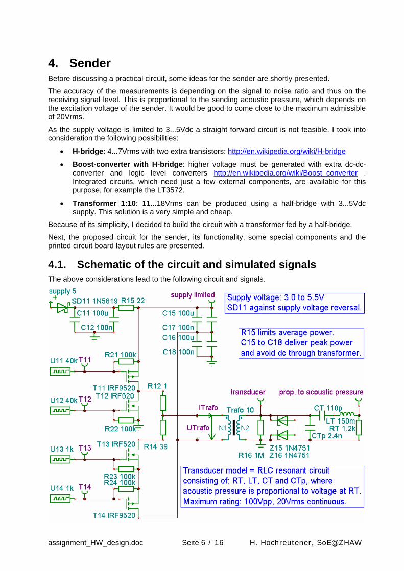
4. Sender Before discussing a practical circuit, some ideas for the sender are shortly presented.
The accuracy of the measurements is depending on the signal to noise ratio and thus on the receiving signal level. This is proportional to the sending acoustic pressure, which depends on the excitation voltage of the sender. It would be good to come close to the maximum admissible of 20Vrms.
As the supply voltage is limited to 3...5Vdc a straight forward circuit is not feasible. I took into consideration the following possibilities:
• H-bridge: 4...7Vrms with two extra transistors: http://en.wikipedia.org/wiki/H-bridge
• Boost-converter with H-bridge: higher voltage must be generated with extra dc-dc-converter and logic level converters http://en.wikipedia.org/wiki/Boost_converter . Integrated circuits, which need just a few external components, are available for this purpose, for example the LT3572.
• Transformer 1:10: 11...18Vrms can be produced using a half-bridge with 3...5Vdc supply. This solution is a very simple and cheap.
Because of its simplicity, I decided to build the circuit with a transformer fed by a half-bridge.
Next, the proposed circuit for the sender, its functionality, some special components and the printed circuit board layout rules are presented.
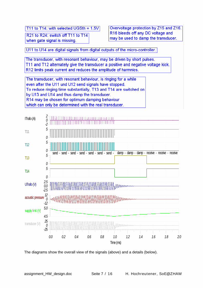
4.1. Schematic of the circuit and simulated signals The above considerations lead to the following circuit and signals.
assignment_HW_design.doc Seite 6 / 16 H. Hochreutener, SoE@ZHAW
T
Time (ms)0.0 0.2 0.4 0.6 0.8 1.0 1.2 1.4 1.6 1.8 2.0
ITrafo (A)-202
T110
5
T120
5
T130
5
T140
5
UTrafo (V)-2.50.02.5
acoustic pressure-12
012
supply limit (V)4.5
5.0
transducer (V)-25
0
receive - receive - receive damp - damp - damp - send - send - send - send - send - send - send -
25
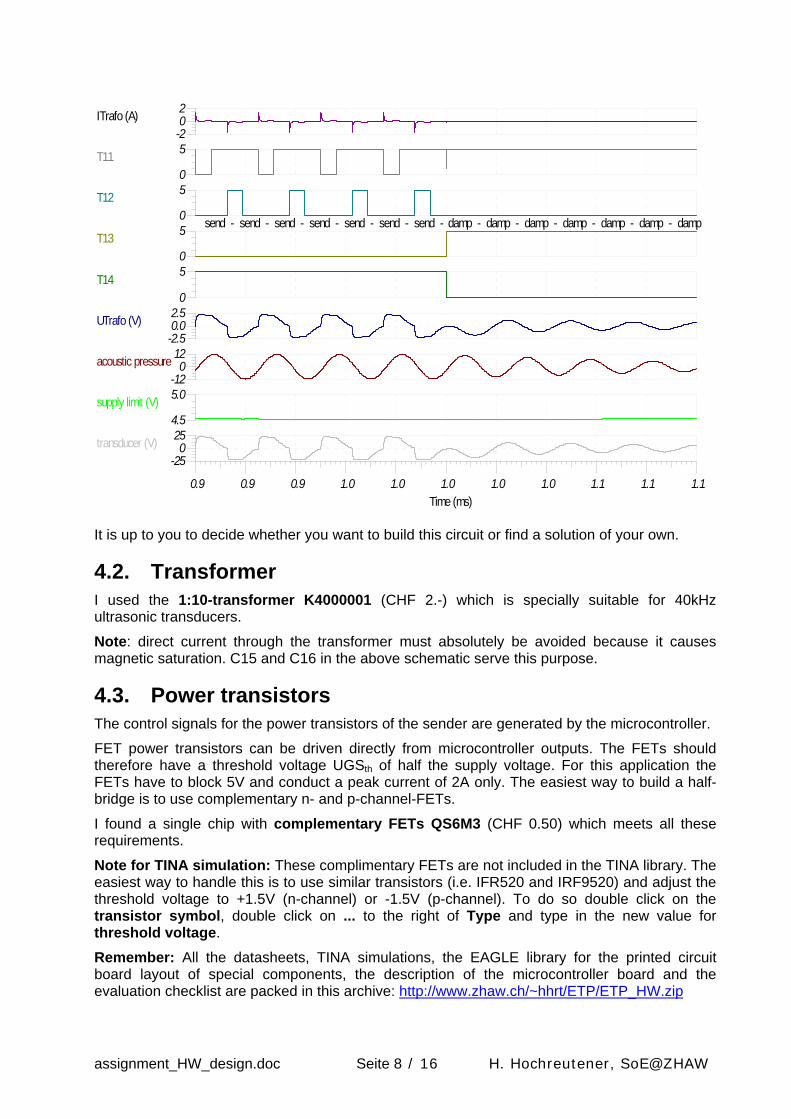
The diagrams show the overall view of the signals (above) and a details (below).
assignment_HW_design.doc Seite 7 / 16 H. Hochreutener, SoE@ZHAW
T
Time (ms)0.9 0.9 0.9 1.0 1.0 1.0 1.0 1.0 1.1 1.1 1.1
ITrafo (A)-202
T110
5
T120
5
T130
5
T140
5
UTrafo (V)-2.50.02.5
acoustic pressure-12
012
supply limit (V)4.5
5.0
transducer (V)-25
0
damp - damp - damp - damp - damp - damp - damp send - send - send - send - send - send - send -
25
It is up to you to decide whether you want to build this circuit or find a solution of your own.
4.2. Transformer I used the 1:10-transformer K4000001 (CHF 2.-) which is specially suitable for 40kHz ultrasonic transducers.
Note: direct current through the transformer must absolutely be avoided because it causes magnetic saturation. C15 and C16 in the above schematic serve this purpose.
4.3. Power transistors The control signals for the power transistors of the sender are generated by the microcontroller.
FET power transistors can be driven directly from microcontroller outputs. The FETs should therefore have a threshold voltage UGSth of half the supply voltage. For this application the FETs have to block 5V and conduct a peak current of 2A only. The easiest way to build a half-bridge is to use complementary n- and p-channel-FETs.
I found a single chip with complementary FETs QS6M3 (CHF 0.50) which meets all these requirements.
Note for TINA simulation: These complimentary FETs are not included in the TINA library. The easiest way to handle this is to use similar transistors (i.e. IFR520 and IRF9520) and adjust the threshold voltage to +1.5V (n-channel) or -1.5V (p-channel). To do so double click on the transistor symbol, double click on ... to the right of Type and type in the new value for threshold voltage.
Remember: All the datasheets, TINA simulations, the EAGLE library for the printed circuit board layout of special components, the description of the microcontroller board and the evaluation checklist are packed in this archive: http://www.zhaw.ch/~hhrt/ETP/ETP_HW.zip
assignment_HW_design.doc Seite 8 / 16 H. Hochreutener, SoE@ZHAW
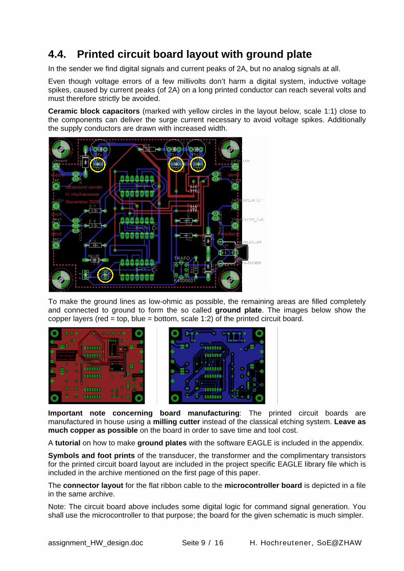
4.4. Printed circuit board layout with ground plate In the sender we find digital signals and current peaks of 2A, but no analog signals at all.
Even though voltage errors of a few millivolts don’t harm a digital system, inductive voltage spikes, caused by current peaks (of 2A) on a long printed conductor can reach several volts and must therefore strictly be avoided.
Ceramic block capacitors (marked with yellow circles in the layout below, scale 1:1) close to the components can deliver the surge current necessary to avoid voltage spikes. Additionally the supply conductors are drawn with increased width.
To make the ground lines as low-ohmic as possible, the remaining areas are filled completely and connected to ground to form the so called ground plate. The images below show the copper layers (red = top, blue = bottom, scale 1:2) of the printed circuit board.
Important note concerning board manufacturing: The printed circuit boards are manufactured in house using a milling cutter instead of the classical etching system. Leave as much copper as possible on the board in order to save time and tool cost.
A tutorial on how to make ground plates with the software EAGLE is included in the appendix.
Symbols and foot prints of the transducer, the transformer and the complimentary transistors for the printed circuit board layout are included in the project specific EAGLE library file which is included in the archive mentioned on the first page of this paper.
The connector layout for the flat ribbon cable to the microcontroller board is depicted in a file in the same archive.
Note: The circuit board above includes some digital logic for command signal generation. You shall use the microcontroller to that purpose; the board for the given schematic is much simpler.
assignment_HW_design.doc Seite 9 / 16 H. Hochreutener, SoE@ZHAW
5. Receiver This chapter is about possibilities and constraints for the receiver and amplifier design.
5.1. Gain control The signal from the receiver can be as low as 0.4mV and as high as 200mV. Ideally the signal at the analog-to-digital converter input is about 1V. This calls for an amplifier with adjustable gain.
Note: The signal levels, the minimum gain of 5 and the maximum gain of 250 are determined using the link budget calculation some pages above.
I considered the following solution possibilities to meet the signal level variation:
• 16bit analog-to-digital converter and fixed gain of 5: The small 0.4mVpp signal yields only 5 significant bits, which is enough for simple pulse edge detection. Availability of required sampling rate at 16-bit resolution must be checked and a noiseless circuit design is crucial. The variable gain could thus be replaced by a sophisticated software algorithm.
• Programmable gain amplifier: As the distance is proportional to elapsed time, the gain is a function not only of distance but also of time. The gain could be set by the micro-controller as a function of time: gain = A0⋅time. The advantage of this solution is the flexibility allowing for more sophisticated software algorithms
• Programmable resistor in the feedback path of the operational amplifier. The resistor value could be set by the micro-controller as a function of time: R = R0⋅time. We suggest using the digital potentiometer AD8400ARZ100 with 256 positions. Note: Datasheet and eagle library are also included in the archive mentioned on the first page of this paper. The advantage of this solution is the flexibility allowing for more sophisticated software algorithms.
• Automatic gain control (AGC) with analog circuitry: A J-FET can be used as voltage controlled resistance in the feedback path of the operational amplifier to adjust the gain to a predefined output signal level. Note: Datasheet and eagle library of the J-FET 2N5458 are also included in the archive mentioned on the first page of this paper. The advantage of this solution is that all the transducer tolerances and variations in reflection factor are automatically ironed out.
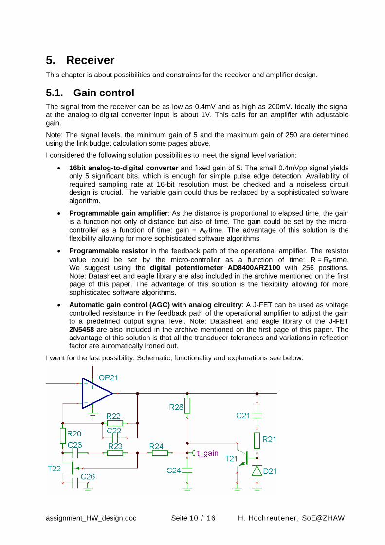
I went for the last possibility. Schematic, functionality and explanations see below:
assignment_HW_design.doc Seite 10 / 16 H. Hochreutener, SoE@ZHAW

The gain of the non-inverting operational amplifier circuit is vU = 1+R22/(R(T22)+R20). R(T22) is a function of the gate-source-voltage UGS: UGS = 0 => R(T22) is small => vU = high (limited by op amp and R20) UGS < -1.5V (pinch off) => R(T22) is ∞ => vU = 1
R24, R23 and C23 perform linearization of the J-FET characteristic for both signal polarities. C26 is for decoupling only and has no influence on the gain. Stability improvement: R20 limits maximum gain and C22 prevents high frequency oscillation.
R28 charges C24 slowly when T21 is blocking. UGS goes towards 0 and gain increases steadily. The time constant can be adjusted by changing the value of R28.
C21, R21, D21 and the base-emitter-diode of T21 form a full wave rectifier. When the voltage at the output of the operational amplifier is above 2⋅0.6V = 1.2Vpp T21 gets a base current and discharges C24 rapidly. UGS gets more and more negative and gain decreases steadily until the output voltage sinks to 1.2Vpp. The time constant can be adjusted by changing the value of R21.
T
edge detection
increasegain
reducegain
Time (1ms)0 1 2 3 4 5 6 7 8 9 10
Input (V)
-50m
0
50m
Output (V)
31m12345
t_gain (V)
0.0
2.5reducegain
edge detection
increasegain
gain = 150 gain = 15gain = 15
As can be seen in the simulation, the whole circuit adjusts gain automatically as to reach 1.2Vpp output signal amplitude, regardless of the input signal level.
The gain adjustment regulation time can be seen well in the timing diagram. These have to be properly chosen. Decreasing gain to fast makes the system vulnerable to noise spikes; decreasing gain to slow yields a square signal at the output. Increasing gain to fast amplifies the noise to much; increasing gain to slow results in missing echoes from a far objects.
Most interesting is the fact that the leading edge of a pulse causes the output to rise temporarily well over the reference value which makes it easy to detect the leading edge of an echo.
Note on J-FETs: The datasheet of the 2N5458 specifies a big specimen spread for the pinch-off voltage of -1V...-7V. In order to work correctly the pinch-off voltage must be less than half the supply voltage. Therefore I selected a specimen with UGS(pinch-off) = -1.5V from the 2N5458 stock.
For the simulation with TINA double click on the 2N5458 symbol, double click on ... to the right of Type and change threshold voltage to -1.5V.
5.2. Operational amplifier The requirements for the operational amplifier are: 3...5V single supply, rail-to-rail output and at least 10MHz gain-bandwidth product (= 40kHz⋅250gain). I chose the operational amplifier TLV2631 (CHF 1.80) which just about meets these requirements. Note: Datasheet and footprint are included in the archive mentioned on the first page of this paper.
assignment_HW_design.doc Seite 11 / 16 H. Hochreutener, SoE@ZHAW
Note: The maximum gain of 250 is determined using the link budget calculation above.
Capacitive load (cable, sample and hold circuit) at the operational amplifier output may lead to undesired oscillation tendency. I suggest using a resistor (i.e. 47Ω) between operational amplifier output and analog-to-digital converter input.
Note for TINA simulation: The TLV2631 is not included in the TINA library. The easiest way to handle this is to use a similar operational amplifier, i.e. the LT1037. The LT1037 however has no rail-to-rail output. This can be handled by increasing both supply voltages of the operational amplifier by 1.5V for simulation purposes.
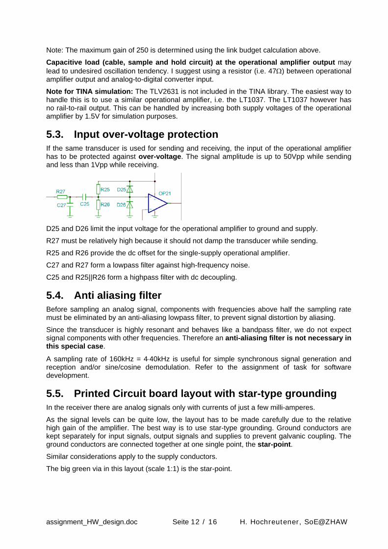
5.3. Input over-voltage protection If the same transducer is used for sending and receiving, the input of the operational amplifier has to be protected against over-voltage. The signal amplitude is up to 50Vpp while sending and less than 1Vpp while receiving.
D25 and D26 limit the input voltage for the operational amplifier to ground and supply.
R27 must be relatively high because it should not damp the transducer while sending.
R25 and R26 provide the dc offset for the single-supply operational amplifier.
C27 and R27 form a lowpass filter against high-frequency noise.
C25 and R25||R26 form a highpass filter with dc decoupling.
5.4. Anti aliasing filter Before sampling an analog signal, components with frequencies above half the sampling rate must be eliminated by an anti-aliasing lowpass filter, to prevent signal distortion by aliasing.
Since the transducer is highly resonant and behaves like a bandpass filter, we do not expect signal components with other frequencies. Therefore an anti-aliasing filter is not necessary in this special case.
A sampling rate of 160kHz = 4⋅40kHz is useful for simple synchronous signal generation and reception and/or sine/cosine demodulation. Refer to the assignment of task for software development.
5.5. Printed Circuit board layout with star-type grounding In the receiver there are analog signals only with currents of just a few milli-amperes.
As the signal levels can be quite low, the layout has to be made carefully due to the relative high gain of the amplifier. The best way is to use star-type grounding. Ground conductors are kept separately for input signals, output signals and supplies to prevent galvanic coupling. The ground conductors are connected together at one single point, the star-point. Similar considerations apply to the supply conductors.
The big green via in this layout (scale 1:1) is the star-point.
assignment_HW_design.doc Seite 12 / 16 H. Hochreutener, SoE@ZHAW
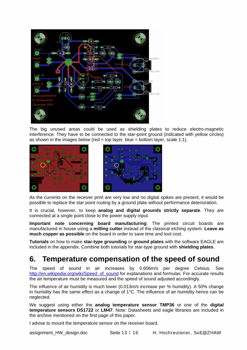
The big unused areas could be used as shielding plates to reduce electro-magnetic interference. They have to be connected to the star-point ground (indicated with yellow circles) as shown in the images below (red = top layer, blue = bottom layer, scale 1:1).
As the currents on the receiver print are very low and no digital spikes are present, it would be possible to replace the star point routing by a ground plate without performance deterioration.
It is crucial, however, to keep analog and digital grounds strictly separate. They are connected at a single point close to the power supply input.
Important note concerning board manufacturing: The printed circuit boards are manufactured in house using a milling cutter instead of the classical etching system. Leave as much copper as possible on the board in order to save time and tool cost.
Tutorials on how to make star-type grounding or ground plates with the software EAGLE are included in the appendix. Combine both tutorials for star-type ground with shielding plates.
6. Temperature compensation of the speed of sound The speed of sound in air increases by 0.606m/s per degree Celsius. See http://en.wikipedia.org/wiki/Speed_of_sound for explanations and formulas. For accurate results the air temperature must be measured and the speed of sound adjusted accordingly.
The influence of air humidity is much lower (0.013m/s increase per % humidity). A 50% change in humidity has the same effect as a change of 1°C. The influence of air humidity hence can be neglected.
We suggest using either the analog temperature sensor TMP36 or one of the digital temperature sensors DS1722 or LM47. Note: Datasheets and eagle libraries are included in the archive mentioned on the first page of this paper.
I advise to mount the temperature sensor on the receiver board.
assignment_HW_design.doc Seite 13 / 16 H. Hochreutener, SoE@ZHAW
7. Testing Everybody agrees that testing is important. But it is often done in an inappropriate way:
• If it doesn’t smell burnt, it’s ok.
• Just check if some signal comes out of the circuit.
• Do hundreds of measurements and pick out the one that looks fine.
• Documentation of tests is waste of time.
It is far better to do only a few, well planned, meticulously documented and reproducible tests to prove that the circuit fulfills the specifications.
Please establish a test plan with distinctive test scenarios.
For the sender the following could be a good approach:
• What wave form is expected at the drains of the “send” transistors T11 and T12? What waveform does actually show up? If there are any differences, give an explanation and prove it with measurements or simulations.
• What signal amplitude and waveform is expected at the transmitter. What does the test say?
• Does the transmitter produce any sound at all? Does the receiver signal level at a defined distance correspond to the calculated value? This can easily be checked with a second transducer connected to an oscilloscope.
• What wave form is expected at the sources of the “damp” transistors T13 and T14?
• Does the ringing of the transmitter correspond to the datasheet and the simulation when T13 and T14 are switched off?
• Is the power consumption according to expectation?
• Repeat each test for 3V instead of 5V supply voltage.
For the documentation of the tests a table could be useful:
Test Expected Measured Difference Remark/Explanation
Waveform at drains of T11 and T12
rectangular: 0V and 5V
rounded shape: 0V and 4.5V T
Time (s)900u 910u 920u 930u 940u 950u
5.0
T11,T12 (V)
0.0
2.5
4.5V instead of 5.0V
not really rectangular
voltage loss across SD11 and R15
T11 is on for 25% both are off for 25%T12 is on for 25% both are off for 25%both off => floating
Signal at transducer
same wave form as at drains of T11 and T12, but amplitude⋅10, no dc offset
... ... ...
... ... ... ... ...
Do set up meaningful tests for the receiver and the temperature sensor in the same manner.
assignment_HW_design.doc Seite 14 / 16 H. Hochreutener, SoE@ZHAW
8. Appendix 8.1. PCB-SW EAGLE: design rules, ground and symbols Note: We have a full licence of EAGLE 4.16r2. Newer versions are not backward compatible.
Download the PCB software EAGLE (PCB = printed circuit board) from http://www.cadsoft.de/download.htm (new version if you use your own computer only) or from ftp://ftp.cadsoft.de/eagle/program/ (version 4.16r2 for compatibility with school computers).
EAGLE can be used as freeware with these limitations: maximum size 100 x 80mm, 2 layers
8.1.1. Design rules I changed the design rules for wider conductor strips and clearances. This minimizes the etching faults and eases dramatically soldering and error detection.
Proceed as follows: in the EAGLE Control Panel double-click on Design-Regeln, then on default.dru. Change the values of these register/entries:
Register Entry Original value Changed to Clearance Different Signals 8mil 16mil Sizes Minimum Width 10mil 24mil Restring Pads Min,Max 10mil, 20mil 20mil, 40mil Restring Vias Min,Max 8mil, 20mil 20mil, 40mil
For information: Measuring unit conversion: 1mil = 0.0254mm 1mm = 40mil
These values/rules apply to the auto-router and the design-rules-check.
It is always possible to increase or decrease the width of conductors or accept small clearances manually for special cases.
8.1.2. Ground plate (digital): property settings for the GND-polygon The outer limit of the ground plate is defined by drawing a polygon. Some properties of the polygon must be changed:
Width 0.024 Spacing 0.05 Isolate 0.05 Name GND
Execute the Ratsnest command to fill the ground plate.
This command should be executed again after changing anything on the PCB layout or when the PCB is opened in EAGLE the next time.
8.1.3. Star-type grounding for analog circuitry: how to proceed • Place a big via near the supply connector and the sieving/blocking capacitors.
• Determine which ground signals must be kept separately: input signal ground, output signal ground, supply ground, ...
• Route each of these grounds manually to the star-point via. You may wish to use a wider conductor size in order to reduce the ohmic resistance.
• Maybe you want to do the same thing for the supply conductors.
• When you have routed all the grounds, use the auto-routing command to route the remaining conductors.
assignment_HW_design.doc Seite 15 / 16 H. Hochreutener, SoE@ZHAW
8.1.4. Ground connections: digital - supply - analog If a circuit consists of mixed digital and analog circuit portions, their ground signals must be kept strictly separate to reduce crosstalk. Otherwise, the digital clock may interfere severely on the analog signal.
The 3GND device from the ground-junctions library serves this purpose. The three ground types are kept apart and connected at just one single spot by soldering bridges in vicinity to the power supply input.
8.2. Related documents: datasheets, simulations, footprints All the documents mentioned in this paper such as datasheets, TINA simulations, the EAGLE library for the printed circuit board layout of special components, the description of the microcontroller board and the evaluation checklist are packed in this archive: http://www.zhaw.ch/~hhrt/ETP/ETP_HW.zip
8.3. Table of contents for the intermediate report The intermediate report HW for ultrasonic distance meter in English has to be delivered printed out and also sent by email.
Use this suggestion (and the checklist evaluation_HW_report.pdf) as a guideline:
• Abstract
• Table of contents
• Introduction
• Specification, functional descriptions and block diagrams
• Sender
o Solution possibilities with advantages and drawbacks
o Justification for chosen implementation, circuit design, important formulas
o Description of the schematics, the inputs and outputs
o Test scenarios with expected results, actual performance and interpretation
o PCB layout, bill of material, commissioning, instruction manual
• Receiver
o points similar to sender
• Temperature sensor
o points similar to sender where appropriate
• Achieved results, outlook and reflection
• Appendix
Hint: The appendix contains all the information that is not needed for fluent reading of the documentation. As a general rule, diagrams go in the main text, data tables in the appendix.
assignment_HW_design.doc Seite 16 / 16 H. Hochreutener, SoE@ZHAW