assessing cres performance for on-line cleaning optimization
TRANSCRIPT
Assessing CRES Performance for On-line Cleaning Optimization
Jerry Broz, Ph.D.Seyedsoheil Khavandi
Gene HumphreyWW Applications Engineering
International Test Solutions, Inc.
Silicon Valley Workshop - 2011
Overview
Silicon Valley Workshop - 2011
Background
Problem – Wafer Yield FalloutProbe cleaning is neededEffects of aggressive cleaning (technical and commercial)
Challenge – Choosing a Cleaning ProcessOn-line process development is becoming difficultMethodology for cleaning recipe development
Implementation – Customer Benefits
Summary
2
International Test Solutions – Who are we?
Silicon Valley Workshop - 2011
Global supplier of highly engineered on-line and off-line cleaning materials for wafer sort and package test industries.
Cost-effective cleaning solutions and related technical support services focused on improvement solutions.Patented processes and materials (UPTO 6,777,966 and 7,202,683)Pending US and International IP applications for front-end, wafer-sort, and back-end testing.
“Manufacturing Center” for advanced polymer materialsControlled Compliance Technology (CCT) manufacturing methods.Materials characterization, development, and testing laboratories.
“Test Analysis Center” for performance characterization.Analytical laboratory focused on CRES performance testing.Probe technology and cleaning recipe assessment with optimization.
3
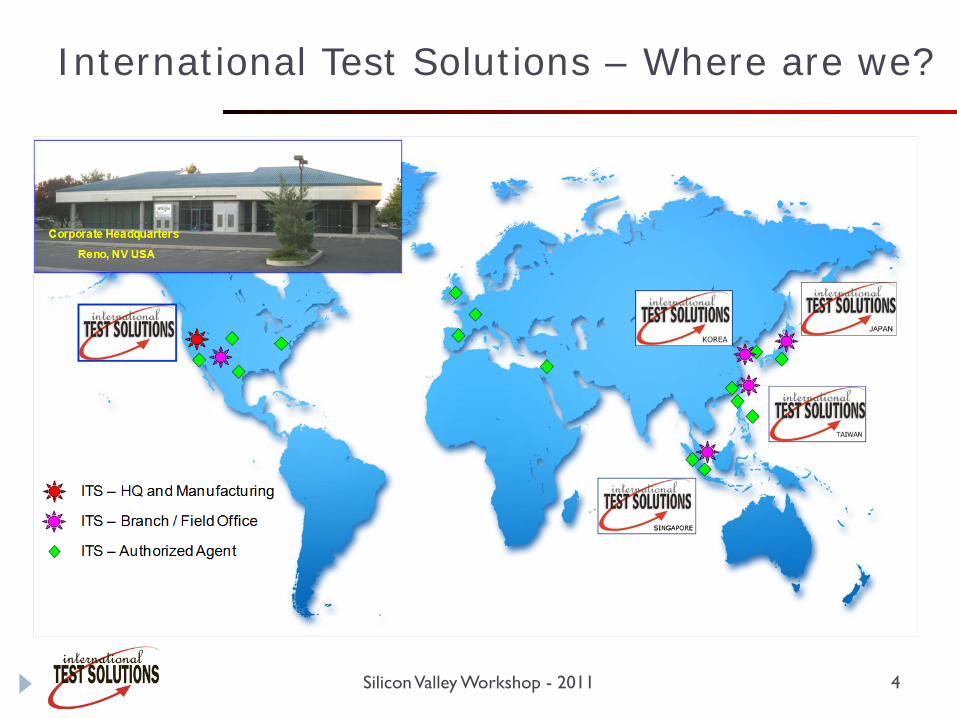
International Test Solutions – Where are we?
Silicon Valley Workshop - 2011 4

Background
Silicon Valley Workshop - 2011
Contact technologies have become advanced; however, the basics of wafer sort and package test have not really changed.
ALL contactor technologies have a type of “tip” which makes physical contact with the various I/O’s of the DUT.
“Contact and slide” is CRITICAL to break surface oxide(s), but creates some level of localized plastic deformation
Physical damage, a.k.a., “probe mark” affects bondability, packaging, assembly, long term reliability, etc.Amount of material displaced or transferred is a complex function of operational settings, metallic interaction, and tribological properties.
5

Adherent Materials Accumulation
Probe Mark 3D Profile ofDisplaced Pad Material
Aluminum
Adherent Material
Silicon Valley Workshop - 2011 6Broz et al., SW Test 2006
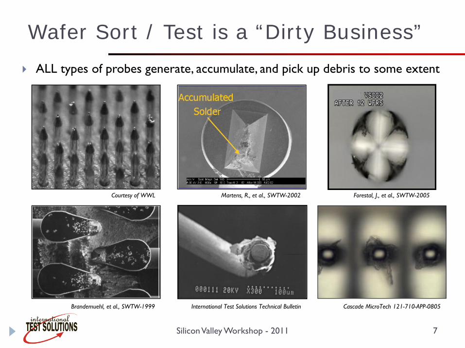
Wafer Sort / Test is a “Dirty Business”ALL types of probes generate, accumulate, and pick up debris to some extent
Courtesy of WWL Martens, R., et al., SWTW-2002 Forestal, J., et al., SWTW-2005
Brandemuehl, et al., SWTW-1999 Cascade MicroTech 121-710-APP-0805
Silicon Valley Workshop - 2011 7
International Test Solutions Technical Bulletin

Contamination Affects Contact Resistance (CRES)
Contact Resistance (CRES) a CRITICAL parameter in wafer sort
CRES affected by two primary parameters“Metal on Metal Contact” between a probe tip and the pads, bumps, pillars, etc.Non-conductive film resistance that interferes with the “Metal on Metal Contact”
ρpad, ρprobe, σfilm = resistivity valuesH = hardness of the pads, bumps, pillars, etc.P = contact pressure applied by probe
Unstable CRES and first pass yield stability is affected film resistance (σfilm) due to build-up of non-conductive materials on the probe tip contact .
( )P
H
PH
4CRES
filmpadprobe σπρρ+
+=
METALLIC CONTACT FILM RESISTANCE
Silicon Valley Workshop - 2011 8
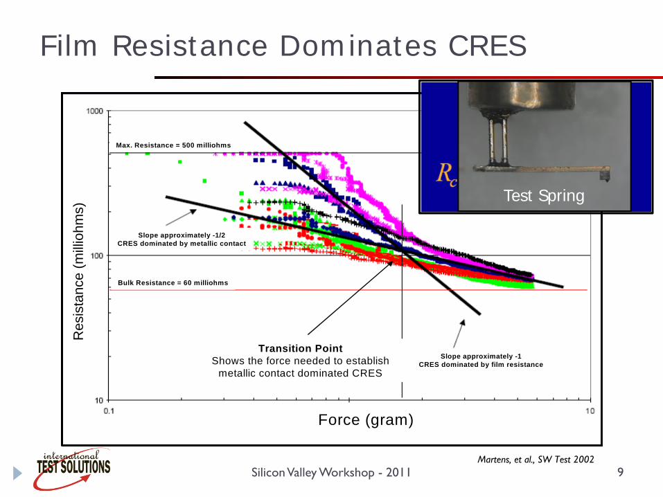
Film Resistance Dominates CRES
Force (gram)
Res
ista
nce
(milli
ohm
s)
Max. Resistance = 500 milliohms
Bulk Resistance = 60 milliohms
Slope approximately -1/2CRES dominated by metallic contact
Slope approximately -1CRES dominated by film resistance
Transition PointShows the force needed to establish
metallic contact dominated CRES
Martens, et al., SW Test 2002
Test Spring
Silicon Valley Workshop - 2011 9
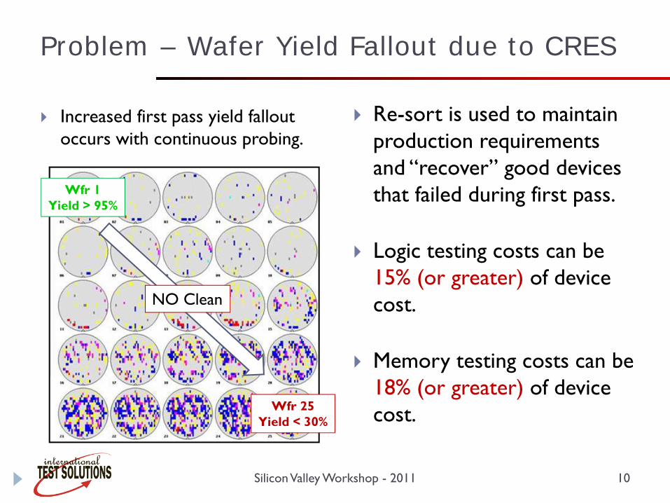
Problem – Wafer Yield Fallout due to CRES
Increased first pass yield fallout occurs with continuous probing.
Re-sort is used to maintain production requirements and “recover” good devices that failed during first pass.
Logic testing costs can be 15% (or greater) of device cost.
Memory testing costs can be 18% (or greater) of device cost.
Silicon Valley Workshop - 2011 10 10
Wfr 1Yield > 95%
Wfr 25Yield < 30%
NO Clean
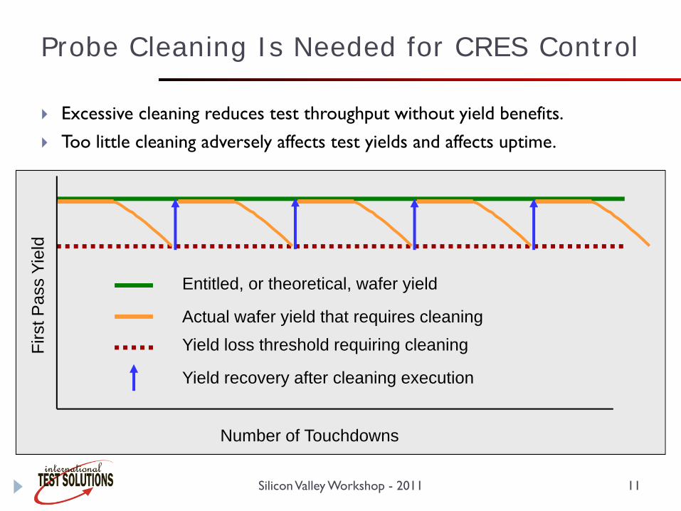
Excessive cleaning reduces test throughput without yield benefits.
Too little cleaning adversely affects test yields and affects uptime.
Entitled, or theoretical, wafer yield
Yield loss threshold requiring cleaningFirs
t Pas
s Yi
eld
Actual wafer yield that requires cleaning
Yield recovery after cleaning execution
Number of Touchdowns
Probe Cleaning Is Needed for CRES Control
Silicon Valley Workshop - 2011 11
Silicon Valley Workshop - 2011
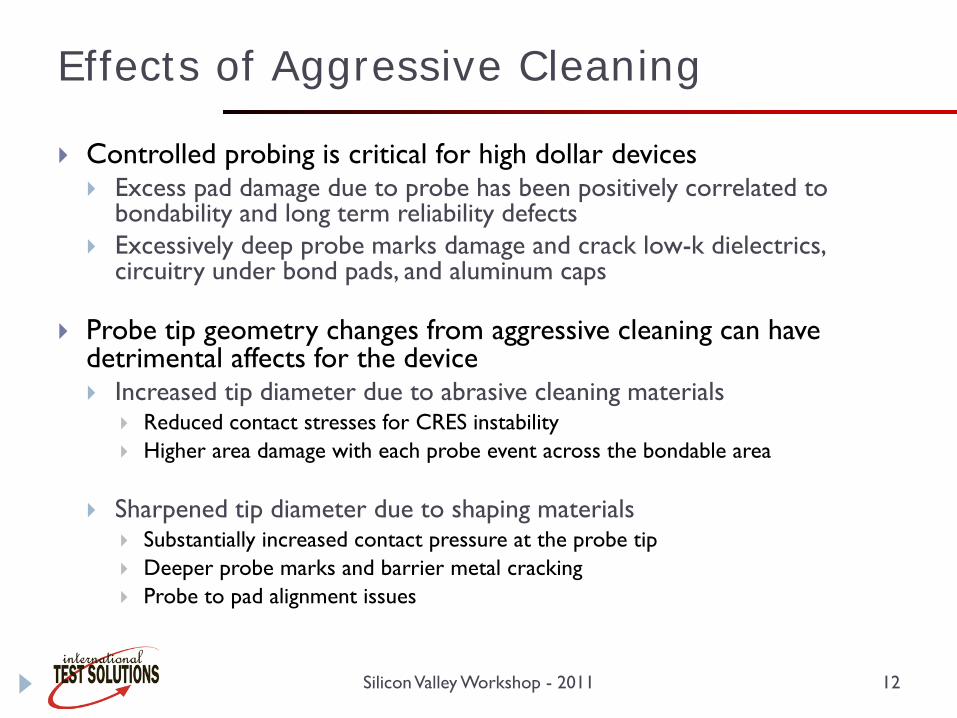
Controlled probing is critical for high dollar devicesExcess pad damage due to probe has been positively correlated to bondability and long term reliability defectsExcessively deep probe marks damage and crack low-k dielectrics, circuitry under bond pads, and aluminum caps
Probe tip geometry changes from aggressive cleaning can have detrimental affects for the device
Increased tip diameter due to abrasive cleaning materialsReduced contact stresses for CRES instabilityHigher area damage with each probe event across the bondable area
Sharpened tip diameter due to shaping materialsSubstantially increased contact pressure at the probe tipDeeper probe marks and barrier metal crackingProbe to pad alignment issues
12
Effects of Aggressive Cleaning
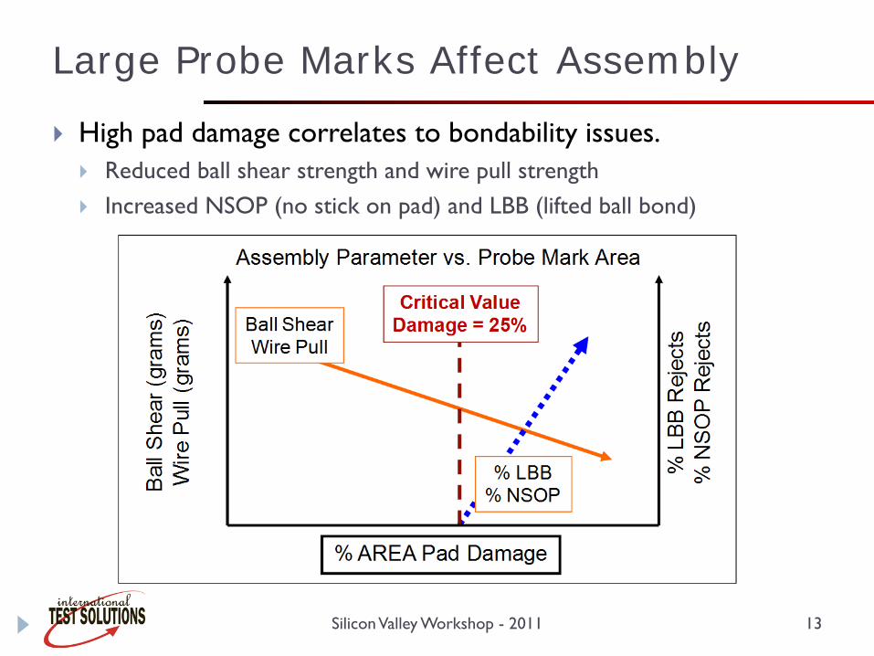
High pad damage correlates to bondability issues.Reduced ball shear strength and wire pull strengthIncreased NSOP (no stick on pad) and LBB (lifted ball bond)
Silicon Valley Workshop - 2011 13
Large Probe Marks Affect Assembly
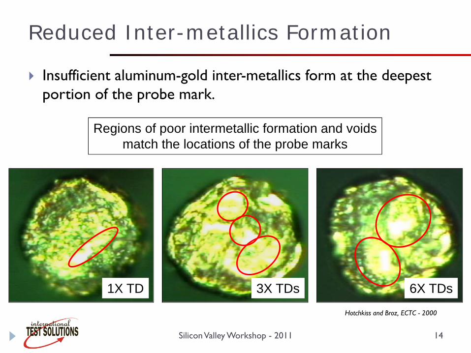
Insufficient aluminum-gold inter-metallics form at the deepest portion of the probe mark.
3X TDs 6X TDs
Regions of poor intermetallic formation and voidsmatch the locations of the probe marks
1X TD
Silicon Valley Workshop - 2011 14
Hotchkiss and Broz, ECTC - 2000
Reduced Inter-metallics Formation

Pad pile-up is correlated to bondability issues.Reduced ball shear strength and wire pull strengthIncreased NSOP (no stick on pad) and LBB (lifted ball bond)
Deep Marks Affect Assembly
Silicon Valley Workshop - 2011 15

Pad Cracking Affects Reliability
Harsh Wafer ProbingProbe mark size increasesProbe mark depth increases% of pads cracked increasesNumber and length of cracks increases
250 µ² 320 µ² 510 µ²
(mils)
Probe Mark Area
2mils OD 3mils OD 4mils OD
Hunter, et al., SW Test 2011
1 TD
Silicon Valley Workshop - 2011 16

17
Poor Cleaning Has Commercial Implications
Silicon Valley Workshop - 2011 17

Challenge – Choosing a Cleaning Process
18Silicon Valley Workshop - 2011 18
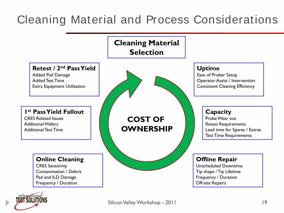
Cleaning Material and Process Considerations
UptimeEase of Prober SetupOperator Assist / InterventionConsistent Cleaning Efficiency
CapacityProbe Wear outRetest RequirementsLead time for Spares / ExtrasTest Time Requirements
Online CleaningCRES SensitivityContamination / DebrisPad and ILD DamageFrequency / Duration
Offline RepairUnscheduled DowntimeTip shape / Tip LifetimeFrequency / DurationOff-site Repairs
Retest / 2nd Pass Yield Added Pad DamageAdded Test TimeExtra Equipment Utilization
1st Pass Yield FalloutCRES Related IssuesAdditional WafersAdditional Test Time
Cleaning MaterialSelection
COST OF OWNERSHIP
Silicon Valley Workshop - 2011 19

Cleaning Process / Recipe Development
Production sort floors are often manpower, materials, and financially limited for detailed characterization studies.
Testing with “full-build” probe cards is expensive and often not feasible, particularly with large array probe cards.
Assessing combinations of key probe process parameters requires substantial resource allocation.
Gaining key insights with a representative test vehicles can be performed quickly under known and controlled conditions.
Probe engineers need “a reasonable starting point” from which to develop on-line cleaning processes.
Silicon Valley Workshop - 2011 20

Testing System OverviewVariable xyz speed and xyz-acceleration.Low probe force measurements.Synchronized load vs. overtravel vs. CRES data acquisition.High resolution video imaging.Current measurement with Keithley source-meter.Micro-stepping to maximize touchdowns.Multi-zone cleaning functions.
Precision Stages
Motion ControlData Acquisition
Probe characterization and cleaning performance testing.
Martens, Allgaier, and Broz , SW Test 2008
Test Under Controlled Test Conditions
Silicon Valley Workshop - 2011 21

Use of Advanced Characterization Tools
Hitachi SEM with EDS capabilitiesCleaning material, probe, device, solder ball, and bond pad imagingElemental surface analysis and assessment.
Veeco 3D Confocal / Metallurgical Microscope Imaging SystemNon-contact, high magnification surface characterization.Cleaning material, probe tip, and probe mark inspection / quantification.
Silicon Valley Workshop - 2011 22

Test vehicle installedonto load cell
High resolution imagingsystem for video acquisition Probe / Material Interaction
and Buckling Visualization
Martens, Allgaier, and Broz, SW Test 2008
Silicon Valley Workshop - 2011 23
Test Vehicle and Cleaning Material
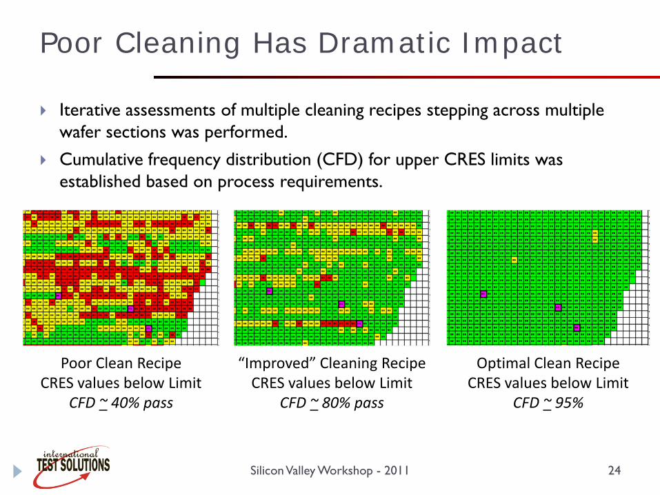
Poor Cleaning Has Dramatic Impact
Silicon Valley Workshop - 2011
Iterative assessments of multiple cleaning recipes stepping across multiple wafer sections was performed.
Cumulative frequency distribution (CFD) for upper CRES limits was established based on process requirements.
Poor Clean RecipeCRES values below Limit
CFD ~ 40% pass
“Improved” Cleaning RecipeCRES values below Limit
CFD ~ 80% pass
Optimal Clean RecipeCRES values below Limit
CFD ~ 95%
24

CFD – Cleaning Process Assessment
After several iterations, cleaning processes were developed for test conditions improved the stability of the CRES.
0.0
20.0
40.0
60.0
80.0
100.0
120.0
0.00 5.00 10.00 15.00 20.00 25.00Contact Resistance (ohms)
Cum
ulat
ive
Perc
enta
ge
CRES ImprovementTrending
CRES SensitivityThreshold
Silicon Valley Workshop - 2011 25
“Cleaning Process Science”
Silicon Valley Workshop - 2011
“Standardized” test method combined with device bond-pad metal touchdowns demonstrated CRES performance.
Iterative cleaning tests with probe test vehicles facilitate cleaning material performance assessment and effective cleaning recipe development under controlled conditions.
On-line optimization and correlation with the test results must be performed at the customer-sites.
26
“Cleaning Process Economics”
For low volume devices and probe card technologies, iterative cleaning process developments are not economical.
Determining cleaning requirement with “full-build” probe cards is often not feasible (or reasonable).
Single touch probes cards warrant special treatment Assessing multiple probe-card technologies is expensiveDemanding electrical requirements may require several different cleaning procedures.
Resources are limited for developing individual cleaning protocols for each probe-card technology and device.
Often a sound “best guess” from past experience is implemented.
Silicon Valley Workshop - 2011 27
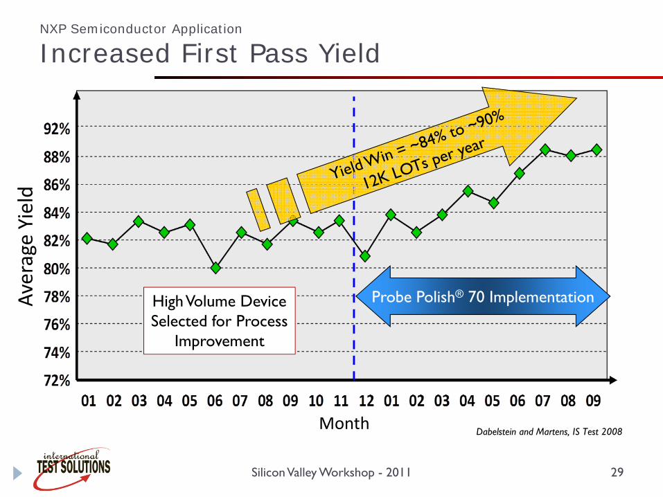
NXP Semiconductor - HamburgHigh volume device sorted with large area array probe cardsInsufficient on-line cleaning to prevent bad performanceFrequent operator intervention and manual on-line cleaningOff-line cleaning and repair time-consuming and expensiveProbe card repair costs were excessive
Objectives for Sort Process ImprovementImplement Probe Polish® based on-line cleaning materials and practices Optimize cleaning to maximize first pass yield and tool utilizationReduce overall probe card repair costs and spares inventory
28Silicon Valley Workshop - 2011 28
Dabelstein and Martens, IS Test 2008
NXP Semiconductor Application
Implementation
Month
Average Yield
NXP Semiconductor Application
Increased First Pass Yield
Probe Polish® 70 Implementation
Silicon Valley Workshop - 2011 29
High Volume DeviceSelected for Process
Improvement
Dabelstein and Martens, IS Test 2008

Event
Month
Probe Polish® 70 Implementation
NXP Semiconductor Application
Reduced Probe Card Repair Events
Silicon Valley Workshop - 2011 30
Large Inventory ofProbe Cards Selected to
Reduce Repair Costs
Dabelstein and Martens, IS Test 2008
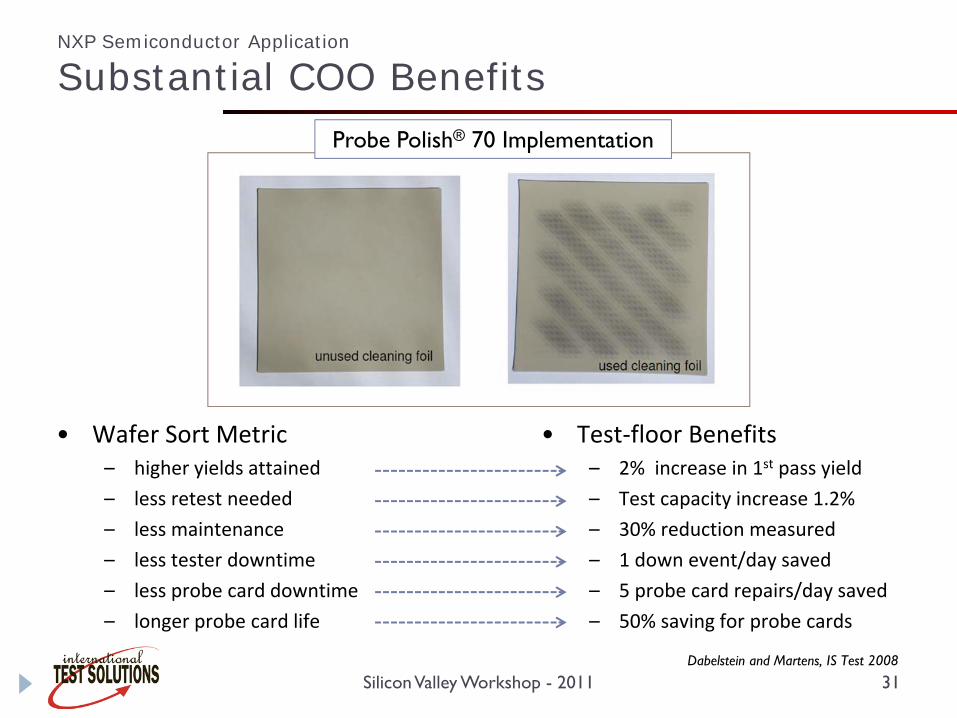
• Wafer Sort Metric– higher yields attained
– less retest needed
– less maintenance
– less tester downtime
– less probe card downtime
– longer probe card life
• Test‐floor Benefits– 2% increase in 1st pass yield
– Test capacity increase 1.2%
– 30% reduction measured
– 1 down event/day saved
– 5 probe card repairs/day saved
– 50% saving for probe cards
NXP Semiconductor Application
Substantial COO Benefits
Silicon Valley Workshop - 2011 31Dabelstein and Martens, IS Test 2008
Probe Polish® 70 Implementation

Summary
For high volume devices, cleaning processes are often optimized to the specific test environment and requirements.
End-Users with multiple probe-card technologies and demanding device requirements may have several different cleaning recipes.
Developing individual cleaning procedures for specific probe-cards and new devices requires extra resource allocation.
ITS has developed a comprehensive suite of tools, methodologies, and infrastructure to provide a critical insights for wafer level test.
Implementing an off-line approach and working with sort-floor engineers can significantly reduce the amount of resources required to develop key aspects of sort processes.
Silicon Valley Workshop - 2011 32

Acknowledgments
ITS WW Applications Team and Sr. Management
ITS Technical PartnersFeinMetallNXP SemiconductorOthers that must remain “nameless”
IEEE SW Test Workshop Archiveshttp://www.swtest.orgAbstract submission for IEEE SW Test 2012 is open !
Silicon Valley Workshop - 2011 33
Thanks for Attending !
Questions ???
Silicon Valley Workshop - 2011 34