asic design for signal processing geoff knagge (9806135) · • the signal processing algorithm,...
TRANSCRIPT

A thesis submitted in partial fulfilment of the requirements for the degree of Bachelor of
Engineering in Computer Engineering at The University of Newcastle, Australia.
ASIC Design for Signal Processing
Geoff Knagge
(9806135)
ASIC Design for Signal Processing
29/05/02 i
Abstract
This thesis describes the methods required to implement a matrix multiplication based algorithm
in hardware. It considers complications such as concurrently updating a matrix while it is being
used for calculations, and developing optimisations for special types of matrices. The goal was
to use some of these multiplications to implement a new signal processing algorithm, of which a
floating point MATLAB model had been provided.
The floating-point model needed to be changed to a fixed-point model, and then implemented in
VHDL. The quantisation of the fixed-point model had to not only provide a small enough error
compared to the optimal result, but also be space efficient when implemented in hardware. To
ensure the correctness of the design, an interface was also needed between the MATLAB model
and the VHDL simulator, so that a test bench could compare the input and output values of each
model. A further concern in chip design is power efficiency, and this formed an extension to the
project, once the basic working design had been created.
This project is an extension to the work that was carried out in an industrial experience project,
between December 2001 and February 2002, with Bell Labs Research. That project was to
create a generically sizable VHDL model of a high speed multiplier, with the goal of meeting
the benchmark of what was thought to be an optimal design. That goal was exceeded, and the
design has since been further enhanced for both this project, and the needs of Lucent
Technologies.
Those multipliers have formed the basis of complex number multipliers, which then formed the
basis of several matrix multiplier designs. Those designs were then analysed, and the most
appropriate ideas were combined to form the arithmetic section of this project. A control unit
was then designed to co-ordinate the unit and interface it to the required memories.
The result is a signal processor that is a fast as possible with the given design specifications.
Furthermore, it contains optimisations to minimise power consumption, and is based on a
multiplier circuit for which a patent has been filed. This document presents a set of techniques
which could ultimately be extended to implement and matrix multiplication based algorithm.

ASIC Design for Signal Processing
29/05/02 ii
Acknowledgements
The opportunity to be able to complete a final year project with a company like Bell Labs
Research has provided highly valuable experience, and has allowed me to extend my knowledge
and skills far beyond what is possible within a university environment. I would like to thank
everyone who has been involved with allowing this to happen, and who assisted me during the
course of my work. In particular:
• Dr Brett Ninness and Dr Steve Weller, of the University of Newcastle, for the time and
effort spent in helping to arrange the industrial experience which later led to the work
described in this thesis.
• Dr Chris Nicol, of Bell Labs Research Sydney, for allowing me to work with his
research team, and especially for the effort in arranging the internship that supported me
for the duration of this project.
• Dr Dave Garrett, of Bell Labs Research Sydney, for providing readily available
guidance and encouragement, as my supervisor for this work.
• Everyone from Bell Labs Research at Lucent Technologies in North Ryde, Sydney.
Almost everyone has provided some form of assistance along the way, and all have
contributed to the great work environment that greatly assisted with working on this
project.

ASIC Design for Signal Processing
29/05/02 iii
Contributions
Work that was contributed by other people:
• The signal processing algorithm, and the associated floating point MATLAB model
• Most of the information provided in Chapter 2. Anything that is not referenced in that
chapter is considered to be general knowledge for this subject matter
• Any other information that is explicitly referenced within this document
• The described patent was based primarily on my own investigations and designs, but
was compiled and filed by Dr Dave Garrett and a Lucent attorney.
Work that I contributed before the commencement of this project:
• Investigation, design, implementation, and testing of various high speed designs for
digital multiplier circuits. The scope of this was only for integers and real numbers.
Work that I contributed as part of this project :
• Generation of the fixed point MATLAB model partly described within this document.
This included all aspects of investigating and resolving the described problems with
quantisation errors and the non-Hermitian nature of quantised matrices.
• Investigation, design, implementation and testing of complex number multiplier circuits
• Enhancements to my existing multiplier designs. This includes the described work on
the designs filed for patent, carried out under the guidance of Dr Dave Garrett and Dr
Chris Nicol.
• Investigation, design, implementation and testing of various matrix multiplier circuits.
While some of the ideas for possible approaches were suggested by my supervisor, Dr
Dave Garrett, the concept behind the design that forms the major part of this project was
entirely my own work.
• All of the described experimentation of varying the parameters of the fixed point model,
and the findings on its behaviour. Much of this work cannot be described within this
document due to the proprietary nature of the algorithm.
• Design, implementation and testing of the signal processing circuit, and the associated
data path and interface. Although not described here, a more general version was also
built, which did not require the matrices to be Hermitian but was slower.
Signed: (student : Geoff Knagge) (Date)
Signed: (Supervisor at Bell Labs Research : Dr Dave Garrett) (Date)
Signed: (Supervisor at University of Newcastle : Dr Brett Ninness) (Date)

ASIC Design for Signal Processing
29/05/02 iv
Table of Contents
����������� � ��������������������������������������������������������������� ��������������������������������������������������������������� ��������������������������������������������������������������� ��� �
���������������������� !�����"� ��������������������������������������������������������������� ��������������������������������������������������������������� ������������������������������� ���
# �������"���%$&�'�(����� ��������������������������������������������������������������� ��������������������������������������������������������������� ������������������������������������������������� �����
)*��������%+ # �����,���&�"� ��������������������������������������������������������������� ��������������������������������������������������������������� ����������������������������������� �.-
/ �102�&�3����4$%���'����� ��������������������������������������������������������������� ��������������������������������������������������������������� ����������������������������������������������� /
5 �&)*����6����������78����&����1$4�&� ��������������������������������������������������������������� ��������������������������������������������������������������� ������������� 9
2.1. Mathematical Background .................................................................... 4 2.1.1. Complex Numbers ..........................................................................................4 2.1.2. Matrices...........................................................................................................5
2.1.2.1 Multiplication............................................................................................5 2.1.2.2 Transpose and Adjoint Matrices ...............................................................6
2.1.3. Hermitian Matrices..........................................................................................6
2.2. Digital Circuit Design............................................................................. 7 2.2.1. ASICs and FPGAs...........................................................................................7
2.2.1.1 FPGAs .......................................................................................................8 2.2.1.2 ASICs ........................................................................................................8
2.2.2. Digital Logic Basics ........................................................................................9 2.2.3. Implementation of gates ................................................................................10 2.2.4. Propagation Delays .......................................................................................11 2.2.5. Power Consumption in Digital Circuits ........................................................11
2.3. Arithmetic in Digital Logic................................................................... 12 2.3.1. Negative Numbers.........................................................................................12 2.3.2. Carry Save Arithmetic...................................................................................12
2.3.2.1 3:2 Compressors......................................................................................14 2.3.2.2 4:2 Compressors......................................................................................15
2.3.3. Booth Multiplication .....................................................................................16 2.3.3.1 Shift and Add Multiplication ..................................................................16 2.3.3.2 Reducing the Number of Partial Products...............................................17 2.3.3.3 Radix-4 Booth Recoding.........................................................................17
2.3.4. Sign Extension Tricks ...................................................................................20
2.4. Synthesis of Digital Circuits ............................................................... 21 2.4.1. Combinatorial Designs..................................................................................21 2.4.2. Synchronous Designs ....................................................................................21 2.4.3. Memories.......................................................................................................23
2.5. Corners ................................................................................................. 23

ASIC Design for Signal Processing
29/05/02 v
������������� ��������������������������! #"%$& (')�*�,+-�� �.�.�/�.�.�.�.�/�.�.�.�.�/�.�.�.�.�/�.�.�.�.�/�.�.�.�.�/�.�.�.� �/�.�.�.�.�/�.�.�.�.�/� 0-1
3.1. Creation of the Fixed Point MATLAB Model ...................................... 24 3.1.1. Performing the Quantisations........................................................................25 3.1.2. The Matrices are Supposed to be Hermitian! ................................................26
3.1.2.1 Quantisation Error...................................................................................26 3.1.2.2 Forcing the Hermitian Property ..............................................................26
3.2. Experimenting with the Fixed Point MATLAB Model ........................ 27 3.2.1. Range and Precision......................................................................................27 3.2.2. “Unstable Algorithms” ..................................................................................28
12����������� ������������������3��4%��5�������,�7689���.�-:��;-�<������� =>�.?@;�6,�A� �.�.�.�.�/�.�.�.�.�/�.�.�.�.�/�.�.�.�.�/�.�.�.�.�/� 0,B
4.1. Beating the Optimal Multiplier ............................................................ 29 4.1.1. Recursive Adder Tree using GENERATE statements..................................29 4.1.2. Adder tree using process statement...............................................................30 4.1.3. Results...........................................................................................................30 4.1.4. Conclusions on multiplier architectures and coding style.............................31 4.1.5. Alternative Algorithms..................................................................................32
4.2. Filed Patent : Power Optimisations Without Affecting Critical Path33
4.3. Complex Number Multipliers .............................................................. 36 4.3.1. Alternative approaches..................................................................................37
4.4. Testing and verification....................................................................... 37
C �84��D<��5�� �<�E�*�-��?F�HGI�768A���.�-/����?�=>�/?@;86,�A�JD �.�.�/�.�.�.�.�/�.�.�.�.�/�.�.�.�.�/�.�.�.�.�/�.�.�.�.�/�.�.�.� �/�.�.�.�.�/�.�.�.�.�/�.�.�.�.�/� �,K
5.1. Fully Parallel Matrix Multipliers .......................................................... 38
5.2. Fully Sequential Matrix Multiplier ....................................................... 40
5.3. Double Buffering Issues...................................................................... 41
5.4. Semi Parallel / Semi Sequential Matrix Multipliers............................ 42 5.4.1. Optimising the Memory Configuration.........................................................43 5.4.2. Implementation of the design........................................................................43
5.4.2.1 Non-conforming matrices.......................................................................44 5.4.2.2 One matrix doesn’ t conform, and the other needs to be overwritten......45
5.5. Squaring Matrices................................................................................ 47
5.6. Multiplying any combination of matrices........................................... 48
5.7. Testing and Verification ...................................................................... 49

ASIC Design for Signal Processing
29/05/02 vi
������������� �� �������������������������������� "!#�%$%%&'&'��! �(�(�(�(�)�(�(�(�(�)�(�(�(�(�)�(�(�(�(�)�(�(�(�(�)�(�(�(�(�)�(� �(�(�)�(�(�(�(�)� *,+
6.1. Ensuring that the output matrices are Hermitian.............................. 51
6.2. Taking Advantage of Hermitian Matrices........................................... 52
6.3. Performing multiplications with Hermitian optimisations................ 53 6.3.1. Multiplication of any Hermitian matrices.....................................................53
6.4. Signal Processor Architecture............................................................ 54
6.5. The Read Stage ................................................................................... 55 6.5.1. Mode 0 – Calculating A = B * B* .................................................................57 6.5.2. Final Mode : Multiplying a 4x4 matrix by a 4x1 matrix...............................59 6.5.3. Other modes : Multiplying two 4x4 matrices ...............................................59
6.6. The Delay Stage ................................................................................... 60
6.7. The Multiplication Stage...................................................................... 61 6.7.1. Mode 0 – Calculating A = B * B* .................................................................62 6.7.2. Other Modes..................................................................................................62
6.8. The Recombine and Output Stage ..................................................... 63 6.8.1. Clamping overflowed values.........................................................................63
6.9. Disabling parts of the matrices........................................................... 64
6.10. Testing and verification..................................................................... 64
6.11. Synthesis of Final Design ................................................................. 65 6.11.1. Changes to described design.......................................................................65
- �/.0����$��21/&/�����3&�����465/7�����3&�����3& �(�(�(�)�(�(�(�(�)�(�(�(�(�)�(�(�(�(�)�(�(�(�(�)�(�(�(�(�)�(�(� �(�)�(�(�(�(�)�(�(�(�(�)�(�(�(�(�)�(�(�(�(�)�(�(�(�(�)� �%�
7.1. Possible Extensions ............................................................................ 67
8 /�#"!#���$%%& �(�(�(�(�)�(�(�(�(�)�(�(�(�(�)�(�(�(�(�)�(�(�(�(�)�(�(�(�(�)�(� �(�(�)�(�(�(�(�)�(�(�(�(�)�(�(�(�(�)�(�(�(�(�)�(�(�(�(�)�(�(�(� �)�(�(�(�(�)�(�(�(�(�)�(�(�(�(�)�(�(�(�(�)�(�(�(�(�)� �%9
: �%��"��4��;7 : �,< :>=@?A:CB .@�%4% �(�(�(�(�)�(�(�(�(�)�(�(�(�(�)�(�(�(�(�)�(�(�(�(�)�(�(�(�(�)�(� �(�(�)�(�(�(�(�)�(�(�(�(�)�(�(�(�(�)�(�(�(�(�)�(�(�(�(�)�(�(�(� �)� �D
A.1. Fixed Point Model................................................................................ 69 A.1.1 Fixed Point Data Type...................................................................................69
A.1.1.1 Staticfixed_pt_matrix .............................................................................69 A.1.1.2 ctranspose...............................................................................................70 A.1.1.3 display ....................................................................................................70 A.1.1.4 minus......................................................................................................70 A.1.1.5 mrdivide .................................................................................................70 A.1.1.6 mtimes....................................................................................................71 A.1.1.7 plus.........................................................................................................71 A.1.1.8 valof ........................................................................................................71
A.1.2 Output of test data to a file............................................................................72

ASIC Design for Signal Processing
29/05/02 vii
�������������� ������������������! "��#%$&�'������(����)���� * ���,+��-���-./�0��� �1�1�1�1�2�1�1�1�1�2�1�1�1�1�2�1�1�1�1�2� 354
B.1. Read Stage........................................................................................... 74 B.1.1 Mode 0 – Multiplication of B * B* ................................................................74 B.1.2 Final Mode : Multiplication of a 4x4 matrix by a 4x1 matrix.......................75 B.1.3 Other Modes : Multiplication of Two 4x4 Hermitian Matrices....................75
B.2. Multiplication Stage............................................................................. 76 B.2.1 Mode 0 : Multiplication of B * B* ..................................................................76 B.2.2 Other modes...................................................................................................77
B.3. Output Stage........................................................................................ 78
�������������76,��89�� *�:1��'<;�=?>A@"6B���)� �1�2�1�1�1�1�2�1�1�1�1�2�1�1�1�1�2�1�1�1�1�2�1�1�1�1�2�1�1�1�1� �1�1�1�1�2�1�1�1�1�2�1�1�1�1�2�1�1�1�1�2�1�1�1�1�2� 35C
C.1. Multiplier Testbench............................................................................ 79 C.1.1 VHDL Code...................................................................................................79
C.1.1.1 Exhaustive Testbench.............................................................................79 C.1.1.2 Random Testbench.................................................................................81
C.1.2 TCL Scripts ...................................................................................................85 C.1.2.1 Exhaustive Testbench.............................................................................85 C.1.2.2 Random Testbench.................................................................................85
ASIC Design for Signal Processing
29/05/02 1
1. Introduction
The motivation to this project comes from the industrial experience that I completed with Bell
Labs Research (Lucent Technologies) between December 2001, and February 2002. The
primary focus of this research group is wireless communications systems, and the development
of digital chips to meet the demands of the next generation of high performance wireless
technologies. The focus of my work was multipli cation circuits, with the challenge to either
match, or improve on, the speed of a benchmark multiplier that was already in existence in the
Lucent component library. This target was exceeded, with a design that was 14% faster than the
existing multiplier, and in some cases matched the speed of the non-configurable design that
was built i nto the synthesis software.
Multipli cation plays many important roles in wireless digital communications, including
filtering, coding and other signal processing. Furthermore, a multiplier component tends to lie in
the criti cal path of a circuit and consumes a large proportion of the power requirements, so it is
important to find a fast, power eff icient design for use in today’s high speed applications.
However, signal processing rarely uses purely real numbers. Use of the complex number system
is almost unavoidable, as it allows mathematical manipulation of variables that would not
otherwise be possible. Hence, for a multiplier circuit to be of any use in a signal processing
system, it must be extended to handle complex numbers.
Multipli cation is not necessaril y as simple as the product of two numbers, whether they are real
or complex. In signal processing it is often necessary to multiply groups of numbers together, in
particular matrices. Implementation of matrix multipli cation is hard to achieve eff iciently in
terms of both time and space, but is a necessary component of many signal processing
algorithms.
Signal processing itself is an area of research that is constantly undergoing technological
change. In particular, the main focus of the Bell Labs Research group in Sydney is the
development of innovations that will be part of the next generations of wireless
communications. Some of the challenges which face researchers are ways to improve the rate of
data transfer, reduce the amount of power consumption of wireless products, and dealing with
the problems of interference that are inherent in many wireless channels. These factors form the
basis of the requirements for this project.
In particular, a new algorithm as been developed that is planned for use in a research chip that is
currently under development. The project of this thesis has thus been to implement that
algorithm in hardware, by writing a VHDL description of a circuit that can be synthesised into a
chip. The particular nature of the algorithm is proprietary, but it requires a number of matrix
multipli cations, using complex numbers. This thesis therefore explores all of the possible

ASIC Design for Signal Processing
29/05/02 2
multipli cation scenarios, of which a subset has been combined in order to implement the
algorithm.
The following specifications describe the challenge that needed to be met
• Implement the algorithm in a design that uses 8ns clock cycles
• It needs to use as few clock cycles as possible for the matrix multipli cations.
• It needs to employ optimisations to use as littl e power as possible
• It cannot use an excessive amount of space on the chip in which it will be implemented
The design tools which were used included:
• ModelSim VHDL compiler and simulation software
• Cadence and Synopsys synthesis software
• TSMC 0.18µm technology library, used by the synthesis tools to determine the
characteristics of a “real” circuit.
• Artisan Components register file generation tool for creating the memories to hold
matrix data.
This document contains a description of the steps required to achieve this goal.
Chapter 2 outlines the background knowledge required for understanding the implementation of
the design. The mathematical background (section 2.1) to this work includes understanding the
complex number system, matrices, and a special type of matrix, Hermitian matrices. A section
on digital circuit design (2.2) describes how modern digital chips are designed, and some of the
issues that need to be addressed. Additionally, there are special techniques that allow relative
ease of implementation of arithmetical operations in digital hardware, as described in section
2.3. Finally, the descriptive model of the must be converted into an actual circuit to be of any
real use, and section 2.4 covers this process of synthesis.
The original algorithm was modelled in MATLAB software, and used floating point numbers of
a high precision. To meet the needs of simulating a hardware model, the MATLAB code needed
to be changed to implement a fixed point model of limited precision. Chapter 3 reveals some of
the problems and issues that were encountered while working with this simulation.
Chapter 4 provides an overview of the implementation, and optimisation, of the multiplier
circuit that is the basic component of this project. Section 4.1 briefly describes my previous
work on creating a high speed multiplier design, of which more detail can be obtained by
referring to my project report on this task [12]. During the course of this project, additional
work was done on techniques to optimise the design so that a power saving enable function
could be added without affecting the criti cal path. This work has resulted in Lucent fili ng a
patent on my design, and is described in section 4.2. Finally, section 4.3 describes the adaption
of the original multiplier into a design that operates on complex numbers.

ASIC Design for Signal Processing
29/05/02 3
The next step was to investigate designs for matrix multipli cation, which is the subject of
Chapter 5. The first section covers a parallel architecture, which requires a lot of circuitry but is
fast. Conversely, the second section, on a fully sequential architecture, describes an algorithm
that requires minimal circuitry but takes much longer to complete its operation. Section 5.4
describes the architecture that was chosen, using a compromise between the previously
described extreme ends of the spectrum of possibiliti es. The rest of this chapter then covers
special cases that need to be addressed in order to perform special cases of multipli cations, such
as squaring, and optimally writing the output over one of the source matrices.
Once a favoured architecture for matrix multipli cation was chosen, it needed to be incorporated
into a design for a signal processor that could handle many different multipli cations, including
the “problem types” that are addressed in Chapter 5. Chapter 6 describes this implementation in
detail , including how the matrix multiplier can be optimised for the special types of matrices
that are to be used, and the operation of the various functional blocks of the design.
Chapter 7 concludes this document by describing the results and findings obtained, and
describing possibiliti es for further work on this project.
Finally, there a number of appendix pages are included to provide some insight into the actual
design work that was implemented:
• Appendix A contains portions of the MATLAB code that was used to simulate the fixed
point model of the algorithm
• Appendix B contains flow charts, describing the general operation of the different
stages of the signal processor.
• Appendix C consists of samples of some of the code that was written to test the designs
described within this document.

ASIC Design for Signal Processing
29/05/02 4
2. Technical Background
The work described in this document incorporates two distinct components. The first of these is
the mathematical theoretical model of how the signal processor is supposed to work. The second
is the VHDL implementation, which can then be synthesised for incorporation in future chip
designs.
2.1. Mathematical Background
The specified algorithm for this project involves an equation requiring the manipulation of
matrices. Furthermore, these matrices involve arithmetic of complex numbers. Hence, it is
necessary to review the relevant background theory to these topics in order to understand the
detail of the following chapters.
2.1.1. Complex Numbers
[1]
Complex numbers are a superset of the real number set that is most famili ar to people. They
consist of a “real” component, x, and an “ imaginary” component, y, and are written as
z = x + iy
The symbol “ i” designates the imaginary component, and is defined as
1−=i
All further mathematical manipulation, that is required in this project, can be done by simply
treating the “i” symbol li ke any other algebraic variable. Multipli cation of complex numbers is
covered in chapter 4.

ASIC Design for Signal Processing
29/05/02 5
2.1.2. Matrices
[2]
A matrix is simply a table of values, which is typically used to represent sets of simultaneous
equations. For example,
Figure 2-1: Matrices are used to represent sets of simultaneous equations
This system of equation could be then be simpli fied to y = Ax. The notation used for matrices is
that an m x n matrix has m rows and n columns, and that aij represents the value of the cell at
row i and column j.
2.1.2.1 Multiplication
[3]
Multipli cation of matrices is more involved than addition, and requires the following conditions
for the product C = AB :
• The number of rows in A is the same as the number of columns in B
• The number or columns in A is the same as the number of columns in C
• The number of rows in B is the same as the number of rows in B
In summary, (a x b matrix)(b x c matrix) = (a x c matrix).
Given an l x m matrix A, a m x n matrix B, and a l x n matrix C, we can calculate
∑=
=≤≤≤≤∀m
nnjinij BACnjliji
1
,1 and 1|,
That is, for a particular cell i n C, we take the row from A and the column from B that
corresponds to that cell ’ s row and column in C. We then take each pair of elements one at a
time, starting from the left and top respectively, and multiply them together. The final value for
the cell i n C is then the sum of these multipli cations.
++++++
=
+
222313212222122122211121
121313111222121112211111
232221
131211
2221
1211
abbaabbaabba
abbaabbaabba
bbb
bbb
aa
aa
Matrix multipli cation is associative, but generally not commutative.
y1 = a11x1 + a12x2 + … + a1nxn
y2 = a21x1 + a22x2 + … + a2nxn
… ym = am1x1 + am2x2 + … + amnxn
=
mmnmm
n
n
m x
x
x
aaa
aaa
aaa
y
y
y
...
...
............
...
...
...2
1
21
22221
11211
2
1

ASIC Design for Signal Processing
29/05/02 6
2.1.2.2 Transpose and Adjoint Matrices
[4,5]
The transpose of a matrix Q is denoted QT, which can be defined as
jiijT
ji QQQQji ,,, ,|, =∈∀
Such matrices hold the following special property, that can be useful for simpli fying matrix
equations:
( ) TTT ABAB =
A special type of transposed matrix is the adjoint matrix, defined as TAA ≡*
That is, the adjoint of a matrix is made up of the complex conjugate of each element of it’ s
transpose:
jiijji QQQQji ,,*
, ,|, =∈∀
Adjoint matrices also hold the property:
( ) ***ABAB =
Note: The MATLAB notation for the adjoint matrix is A’
2.1.3. Hermitian Matrices
[7,8]
Hermitian matrices are special matrices, characterised by the following qualiti es
• The matrix is square
• The matrix is self-adjoint. This means that for a matrix Q, if Q(a,b) = x + iy, then Q(b,a)
= x – iy.
They contain the following special properties that often allows considerable simpli fication of
matrix equations:
• (A*)* = A
• (A + B)* = A* + B*
• ( ) **AkkA =
• (AB)* = A*B*
• An addition or multipli cation between two Hermitian matrices will produce an answer
that is also Hermitian

ASIC Design for Signal Processing
29/05/02 7
2.2. Digital Circuit Design [9] Digital circuit design was once a process of manual schematic design, involving selection of
individual gates, and determining how they should be physically connected to each other to
achieve the desired function. The problem with this method is that it is slow, tedious, and prone
to error. Furthermore, the design of today’s advanced VLSI (very large scale integration) chips,
such as the AMD and Intel microprocessors used to create this document, would be near
impossible with such methods.
An alternative, that is used is to describe the intended behaviour and architecture of a design, is
by using a high level Hardware Description Language (HDL). The two competing standards,
Verilog and VHDL, are HDLs which allow circuit designs to be represented in a way that is
much more intuiti ve to create and understand. Furthermore, the designs can be created much
more rapidly, and the only errors are li kely to be with the logic design, as opposed to wrongly
connected gates.
HDL designs can then be compiled into a vendor specific encoding, for use with simulation and
testing tools. Then, once the design is believed to work correctly, a synthesis tool processes it, to
produce a design for an ASIC or FPGA chip. The resulting output is analysed for performance
data, the code may be refined and recompiled, and the process is repeated.
Figure 2-2 : Design process for digital circuits. ModelSim and Cadence are specific products which
were used in this project to perform the designated steps in the process.
2.2.1. ASICs and FPGAs [9] Both Application Specific Integrated Circuits (ASICs) and Field Programmable Gate Arrays
(FPGAs) are types of custom chips, which differ in their properties, cost, and in the way that
they are manufactured. The choice of which to use depends on the required application.
VHDLCoding
CompileSimulate
andCheck
SynthesiseDesign Analyse
Results
ModelSimCadence
PKSText Editor
FinalDesign

ASIC Design for Signal Processing
29/05/02 8
2.2.1.1 FPGAs FPGA devices typically contain an architecture that is vendor specific. A major advantage is
that the designer is then able to quickly program them as required, with no additional
manufacturing necessary. If testing fails, then the design can be changed and another device
immediately reprogrammed. In addition, circuit design outside of the chip can be
simultaneously performed, since the function of FPGA pins can be assigned before the internal
design is complete. However, FGPA devices cost on average between US$100 to US$200,
making them relatively expensive for mass production.
2.2.1.2 ASICs Older style ASIC chips initiall y contained arrays of unconnected transistors, created during the
most complex and costly phase of manufacture. Known as “gate arrays” , these contained a set
of basic cells across the chip, which included logic gates, registers, and macro functions such as
multiplexors and comparators. Gate arrays may or may not contain predefined “channels” , used
for routing between the basic cells.
The most common type of ASIC currently used is the standard cell format. These contain no
components and the time of initial manufacture, and do not contain any type of basic cell .
Instead, custom layouts are created for each part of the design, making more eff icient use of the
available sili con.
A final manufacturing process involves the connection of the generic units to form the specified
design, and can take two or more weeks. Individual devices can cost as littl e as US$10, but the
initial engineering costs can be US$20,000 to over US$100,000.
The designs described in this document are targeted for ASIC chips, and make use of the TSMC
0.18µm Standard Cell Library.
ASIC Design for Signal Processing
29/05/02 9
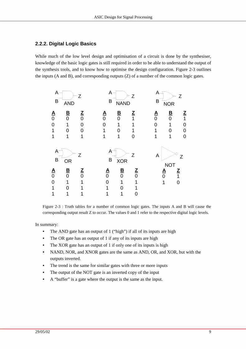
2.2.2. Digital Logic Basics While much of the low level design and optimisation of a circuit is done by the synthesiser,
knowledge of the basic logic gates is still required in order to be able to understand the output of
the synthesis tools, and to know how to optimise the design configuration. Figure 2-3 outlines
the inputs (A and B), and corresponding outputs (Z) of a number of the common logic gates.
A B Z 0 0 0 0 1 0 1 0 0 1 1 1
A B Z 0 0 1 0 1 1 1 0 1 1 1 0
NAND
Z A
B AND
Z A
B NOR
Z A
B
OR Z
A
B Z
A
B XOR
A B Z 0 0 1 0 1 0 1 0 0 1 1 0
A B Z 0 0 0 0 1 1 1 0 1 1 1 1
A B Z 0 0 0 0 1 1 1 0 1 1 1 0
NOT
Z A
A Z 0 1 1 0
Figure 2-3 : Truth tables for a number of common logic gates. The inputs A and B will cause the
corresponding output result Z to occur. The values 0 and 1 refer to the respective digital logic levels.
In summary:
• The AND gate has an output of 1 (“high” ) if all of its inputs are high
• The OR gate has an output of 1 if any of its inputs are high
• The XOR gate has an output of 1 if only one of its inputs is high
• NAND, NOR, and XNOR gates are the same as AND, OR, and XOR, but with the
outputs inverted.
• The trend is the same for similar gates with three or more inputs
• The output of the NOT gate is an inverted copy of the input
• A “buffer” is a gate where the output is the same as the input.

ASIC Design for Signal Processing
29/05/02 10
2.2.3. Implementation of gates Physical logic gates are built with transistors, and the particular characteristics of an individual
gate depend upon the type of transistors used to implement it. For example, the CMOS
implementation of a NOR gate could be represented by figure 2-4.
Figure 2-4 : CMOS implementation of an AND gate
Since they are built from transistors, logic gates inherit a number of characteristics that are
important to digital design:
• All transistors contain some form of capacitance, which affects the speed of the device,
and the power it dissipates.
• Transistors are only capable of supplying a limited amount of power through their
output pins, and all real logic gates consume an amount of current through their inputs.
Therefore, an output of a logic gate can only reliably drive a limited number of inputs
on other gates, and this number is called the fan-out of the gate.
A
B
Z

ASIC Design for Signal Processing
29/05/02 11
2.2.4. Propagation Delays An additional complexity of digital analysis is that the outputs of logic gates do not change
instantaneously with the inputs. Each takes a finite amount of time, known as the propagation
delay, which is caused by the capacitances within the logic gates, and by the fact that a potential
difference cannot instantaneously change. Furthermore, different types of gate are constructed
with different configurations of transistors, so they also vary in their propagation delay.
In any reasonably sized digital asynchronous circuit, there are a large number of possible paths
between the inputs and each of the outputs. The propagation delay for an individual path is the
sum of the propagation delays of the gates through which it passes. The path that has the highest
delay is known as the critical path for the circuit.
2.2.5. Power Consumption in Digital Circuits The power dissipated by a digital circuit becomes an important issue when it is being designed
for use in a chip. This is not only from the practical aspect, that a chip can only withstand a
certain amount of heat generated from power dissipation, but also from the commercial aspect
that lower power products are more competiti ve. There are two broad categories for power
consumption:
• Static power: This is the power used by a logic gate when its output is held at a constant
level. It is caused by leakage currents, which are characteristic to any circuit.
• Dynamic power: Dynamic power is used when a gate is changing state. A small
proportion comes from the switching current generated by the change, but the major
part is due to the charging of the gate’s capacitance to reflect the new voltage level.
Of the two, dynamic power is the most significant, and the one that can be influenced by the
logic design. If the number of transitions in the state of a circuit’s gates can be minimised, then
so will be the power consumption of that circuit. There are a number of ways in which this can
be attempted:
• Disabling unused parts of the circuit. By placing an AND gate in front of each of the
inputs, with one input attached to an enable signal, then the entire circuit will remain in
a static state whilst that enable pin is at a low logic level.
• Reducing glitches in a circuit. A glitch is simply a temporary change in the logic level
of a signal before it reaches its final value. These are often unnecessary if the logic is
arranged appropriately, and removing them can make significant power improvements.

ASIC Design for Signal Processing
29/05/02 12
2.3. Arithmetic in Digital Logic
There are many occasions where the accepted standard methods for manual execution of
arithmetic operations are highly ineff icient when implemented into hardware. Two such
examples are addition and multipli cation.
2.3.1. Negative Numbers
Binary numbers only have 0’s and 1’s, so there is no plus or minus signs. Therefore, to work
with negative numbers, we need a special way of representing these values. One such technique
is called 2’s complement.
A 2’s complement number uses the most significant bit as the “sign bit” , with a “1” indicating a
negative number, and a “0” representing a positi ve number. To take the negative value of a 2’s
complement number, simply:
• Invert all of the bits
• Add 1 to the result.
2.3.2. Carry Save Arithmetic
One of the major speed enhancement techniques used in modern circuits is the abilit y to add
numbers with minimal carry propagation. The basic idea is that three numbers can be reduced to
2, in a 3:2 compressor, by doing the addition while keeping the carries and the sum separate.
This means that all of the columns can be added in parallel without relying on the result of the
previous column, creating a two output “adder” with a time delay that is independent of the size
of its inputs.
10111001
00101010
00111001
Sum: 10101010
Carry: 00111001
Result: 100011100
Figure 2-5 : Example of carry-save arithmetic. A normal adder generates the result at a later stage.
The sum and carry can then be recombined in a normal addition to form the correct result. This
process may seem more complicated and pointless in the above trivial example, but the power
of this technique is that any amount of numbers can be added together in this manner. It is only
the final recombination of the final carry and sum that requires a carry propagating addition.
ASIC Design for Signal Processing
29/05/02 13
Figure 2-6, from [10], is called a Wallace Tree and is one method of combining 3:2 carry save
adders to add together 7 numbers, of size k bits.
Figure 2-6 : Wallace tree method of carry-save arithmetic [10]
The first level of the tree generates two carries and two sums, as well as the left over term,
which is not added. Since the carries from any single column actually means “add one to the
next column” , the carry bits must be shifted left one position before they can be added to the
result. Hence, they are aligned with bits k down to 1.
The two sum values and the leftover term are all aligned with bits k-1 down to 0, so they can be
fed into another 3:2 compressor to form another carry and sum. The three carries can then be
added to form another carry and sum, and all of the results are then pushed into the larger carry-
save adder to produce the final carry and sum. A carry propagate adder, usually an adder using
carry look-ahead, produces the final result.
The above technique arranged the adder tree so that all of the output bits could be obtained
while minimising the size of the circuit. However, in the case of multipliers, we know what the
expected output size will be, and so we can set all of the input and output sizes to that value. We
do not care about any overflowing sign bits, so they can be discarded and the carries can simply
be shifted left to the correct alignment. All of the results can then be grouped together as one
and continually reduced until we are left with two values. This is demonstrated by figure 2-7.

ASIC Design for Signal Processing
29/05/02 14
Figure 2-7: Carry-save adder tree for when overflowing carries from the MSB do not matter This method may appear wasteful because a lot of bits in the first stages of the adder tree will be
frozen to zero. However, these will be optimised during synthesis, and this technique seems to
produce more favourable synthesis results than trying to code the design efficiently.
2.3.2.1 3:2 Compressors
The design of the 3:2 compressor is simple, with the following truth table showing that it is
nothing more than a 3 bit adder:
Inputs Outputs
A B C Sum Carry
0 0 0 0 0
0 0 1 1 0
0 1 0 1 0
0 1 1 0 1
1 0 0 1 0
1 0 1 0 1
1 1 0 0 1
1 1 1 1 1
Table 2-1 : Truth table for the 3:2 compressor. In reality, it is simply a full adder. Adding three k-bit numbers together simply involves an array of k 3:2 compressors, each being
independent of each other, and operating on a single bit position:
Figure 2-8: Architecture of the full word 3:2 compressor, using individual bit 3:2 compressors.
3:2 CSA 3:2 CSA
3:2 CSA
3:2 CSA
3:2 CSA
Carryk Sumk-
1
3:2
ak-1bk1ck-1
Carryk-1 Sumk-
2
3:2
ak-2bk-2ck-
2
Carryk-2 Sumk-
1
3:2
ak-3bk-3ck-3
Carry3 Sum2
3:2
a2 b2 c2
Carry2 Sum1
3:2
a1 b1 c1
Carry1 Sum0
3:2
a0 b0 c0

ASIC Design for Signal Processing
29/05/02 15
2.3.2.2 4:2 Compressors The discussion so far has referred only to 3:2 carry-save adders, but it is also possible to add
four bits in this format. In reality, as ill ustrated in figure 2-9, there are actually five inputs (one
being a carry in), and three outputs (two carries and the sum).
Figure 2-9 : High level view of the 4:2 compressor
The characteristics of the 4:2 compressor are:
o The outputs represent the sum of the five inputs, so it is really a 5 bit adder
o Both carries are of equal weighting (i.e. add “1” to the next column)
o To avoid carry propagation, the value of Cout depends only on A, B, C and D. It is
independent of Cin.
o The Cout signal forms the input to the Cin of a 4:2 of the next column.
The behaviour of the 4:2 compressor is described by table 2-2.
Inputs Cin = 0 Cin = 1
A B C D Carry Sum Carry Sum
Cout
0 0 0 0 0 0 0 1 0 0 0 0 1 0 0 1 0 0 1 0 0 1 0 0 0
0 1 1 0 0
0 0 1 1 0 1 1 0 1 1 0 0 0 1 0 1 1 0 1 0 1 0 0 1
0 1 1 0 1
0 1 1 1 1 1 1 0 1 1 0 1 1 0 1 1
0 1 1 0 1
1 1 1 1 1 0 1 1 1 Table 2-2 : Truth table for the 4:2 compressor cell
4:2
A B C D
Carry Sum
Cin Cout

ASIC Design for Signal Processing
29/05/02 16
A k-bit 4:2 word adder is then formed as shown below, in figure 2-10.
Figure 2-10: Architecture of the full word 4:2 compressor, using individual bit 4:2 compressors.
2.3.3. Booth Multiplication
Booth multipli cation is a technique that allows for smaller, faster multipli cation circuits, by
recoding the numbers that are multiplied. It is the standard technique used in chip design, and
provides significant improvements over the “long multipli cation” technique.
2.3.3.1 Shift and Add Multiplication
A standard approach that might be taken by a novice to perform multipli cation is to “shift and
add” , or normal “ long multipli cation” . That is, for each column in the multiplier, shift the
multipli cand the appropriate number of columns and multiply it by the value of the digit in that
column of the multiplier, to obtain a partial product. The partial products are then added to
obtain the final result, as depicted by figure 2-11.
0 0 1 0 1 1
0 1 0 0 1 1
0 0 1 0 1 1
0 0 1 0 1 1
0 0 0 0 0 0
0 0 0 0 0 0
0 0 1 0 1 1
0 0 1 1 0 1 0 0 0 1
Figure 2-11 : Sample multiplication, using the shift and add technique.
With this system, the number of partial products is exactly the number of columns in the
multiplier.
4:2 4:2 4:2 4:2
Ak-1Bk-1Ck-1Dk-1 Ak-2Bk-2Ck-2Dk-2 A1 B1 C1 D1 A0 B0 C0 D0
Carryk-1 Sumk-2 Sumk-1 Carry2 Sum1 Carry1 Sum0

ASIC Design for Signal Processing
29/05/02 17
2.3.3.2 Reducing the Number of Partial Products
[11] It is possible to reduce the number of partial products by half, by using the technique of radix 4
Booth recoding. The basic idea is that, instead of shifting and adding for every column of the
multiplier term and multiplying by 1 or 0, we only take every second column, and multiply by
±1, ±2, or 0, to obtain the same results. So, to multiply by 7, we can multiply the partial product
aligned against the least significant bit by –1, and multiply the partial product aligned with the
third column by 2:
Partial Product 0 = Multipli cand * -1, shifted left 0 bits (x –1)
Partial Product 1 = Multipli cand * 2, shifted left 2 bits (x 8)
This is the same result as the equivalent “shift and add” method:
Partial Product 0 = Multipli cand * 1, shifted left 0 bits (x 1)
Partial Product 1 = Multipli cand * 1, shifted left 1 bits (x 2)
Partial Product 2 = Multipli cand * 1, shifted left 2 bits (x 4)
Partial Product 3 = Multipli cand * 0, shifted left 3 bits (x 0)
The advantage of this method is the halving of the number of partial products. This is important
in circuit design as it relates to the propagation delay in the running of the circuit, and the
complexity and power consumption of its implementation.
It is also important to note that there is comparatively littl e complexity penalty in multiplying by
0, 1 or 2. All that is needed is a multiplexer or equivalent, which has a delay time that is
independent of the size of the inputs. Negating 2’s complement numbers has the added
complication of needing to add a “1” to the LSB, but this can be overcome by adding a single
correction term with the necessary “1”s in the correct positions.
2.3.3.3 Radix-4 Booth Recoding
To Booth recode the multiplier term, we consider the bits in blocks of three, such that each
block overlaps the previous block by one bit. Grouping starts from the LSB, and the first block
only uses two bits of the multiplier (since there is no previous block to overlap), as ill ustrated by
figure 2-12.
0 1 0 1 1 0 1 0 1 0
Figure 2-12 : Grouping of bits from the multiplier term, for use in Booth recoding. The least
significant block uses only two bits of the multiplier, and assumes a zero for the third bit.

ASIC Design for Signal Processing
29/05/02 18
The overlap is necessary so that we know what happened in the last block, as the MSB of the
block acts like a sign bit. We then consult the table 2-3 to decide what the encoding will be.
Block Partial Product
000 0
001 1 * Multiplicand
010 1 * Multiplicand
011 2 * Multiplicand
100 -2 * Multiplicand
101 -1 * Multiplicand
110 -1 * Multiplicand
111 0 Table 2-3 : Booth recoding strategy for each of the possible block values.
Since we use the LSB of each block to know what the sign bit was in the previous block, and
there are never any negative products before the least significant block, the LSB of the first
block is always assumed to be 0. Hence, we would recode our example of 7 (binary 0111) as
such in figure 2-13.
0 1 1 1 block 0 : 1 1 0 Encoding : * (-1) block 1 : 0 1 1 Encoding : * (2)
Figure 2-13 : Booth recoding for the two partial products with a multiplier term of 0111.
In the case where there are not enough bits to obtain a MSB of the last block, as in figure 2-14,
we sign extend the multiplier by one bit.
0 0 1 1 1 block 0 : 1 1 0 Encoding : * (-1) block 1 : 0 1 1 Encoding : * (2) block 2 : 0 0 0 Encoding : * (0)
Figure 2-14 : Booth recoding for the multiplier term of 00111. In order to obtain three bits in the last
block, we need to sign extend the multiplier by an extra bit.

ASIC Design for Signal Processing
29/05/02 19
The example from figure 2-11 can then be rewritten in the form of f igure 2-15.
0 0 1 0 1 1 , multipli cand
0 1 0 0 1 1 , multiplier
1 1 -1 , booth encoding of multiplier
1 1 1 1 1 1 0 1 0 0 , negative term sign extended 0 0 1 0 1 1
0 0 1 0 1 1
0 0 0 0 1 , error correction for negation
0 0 1 1 0 1 0 0 0 1 , discarding the carried high bit Figure 2-15: An example of a Booth recoded multiplication.
One possible implementation is in the form of a Booth recoder entity, such as the one in figure
2-16, with its outputs being used to form the partial product:
Figure 2-16 : Booth Recoder and its associated inputs and outputs. [7]
In figure 2-16,
• The zero signal indicates whether the multipli cand is zeroed before being used as a
partial product
• The shift signal is used as the control to a 2:1 multiplexer, to select whether or not the
partial product bits are shifted left one position.
• Finally, the neg signal indicates whether or not to invert all of the bits to create a
negative product (which must be corrected by adding “1” at some later stage)
The described operations for booth recoding and partial product generation can be expressed in
terms of logical operations if desired but, for synthesis, it was found to be better to implement
the truth tables in terms of VHDL case and if/then/else statements.
Bo
oth
Rec
ode
r neg
zero
shift (x2)
Bits from multiplier
3

ASIC Design for Signal Processing
29/05/02 20
2.3.4. Sign Extension Tricks
Once the Booth recoded partial products have been generated, they need to be shifted and added
together in the following fashion:
[Partial Product 1]
[Partial Product 2] 0 0
[Partial Product 3] 0 0 0 0
[Partial Product 4] 0 0 0 0 0 0
The problem with implementing this in hardware is that the first partial product needs to be sign
extended by 6 bits, the second by four bits, and so on. This is easily achievable in hardware, but
requires additional logic gates than if those bits could be permanently kept constant, and the
additional logic also consumes more power.
1 1 1 1 1 1 1 0 0 1 0
0 0 0 0 0 1 0 1 1
0 0 0 0 1 0 0
0 1 1 1 0
0 1 1 1 1 0 1 1 1 1 0
Fortunately, there is a technique that achieves this:
• Invert the most significant bit (MSB) of each partial product
• Add an additional ‘1’ to the MSB of the first partial product
• Add an additional ‘1’ in front of each partial product
This technique allows any sign bits to be correctly propagated, without the need to sign extend
all of the bits.
0 1 0 1 0 1 1 (additional “1”s)
0 0 0 1 0
1 1 0 1 1
1 0 1 0 0
1 1 1 1 0
0 1 1 1 1 0 1 1 1 1 0

ASIC Design for Signal Processing
29/05/02 21
2.4. Synthesis of Digital Circuits
Synthesis is the process of converting the VHDL model into an actual circuit design, which can
be implemented in a silicon chip. This is done by a software tool, such as those available from
Synopsys or Cadence, which attempts to produce an optimal layout, subject to the design
constraints set by the user.
2.4.1. Combinatorial Designs
To set the specifications for a purely combinatorial design, we need to create a clock signal,
which is used as a reference for the target speed of the design.
set_clock clk –waveform {0 4.00} –period 8.0
We can then set the other timing constraints, as illustrated in figure 2-17.
Figure 2-17 : Timing constraints for synthesis of an asynchronous circuit.
set_input_delay –clock clk 0.0 [find –ports –inputs *]
set_external_delay –clock clk 0.0 [find –ports –outputs *]
Further constraints that may be set include the fan-out limit, and slew time limit for signals.
With all of these constraints set, the synthesis can begin to optimise both speed and size of the
circuit, with preference given to speed.
2.4.2. Synchronous Designs
Synthesis of synchronous designs is very similar to the combinatorial designs, except that a
clock signal is already present. The consequence of this is that we need to make the synthesis
tool aware of this signal, and take steps to ensure that clock skewing does not occur.
The assumption in any synchronous design is that the clock signals arrive at their destinations
simultaneously. Clock skewing is the phenomenon where some clock signals arrive faster than
others, and therefore some parts of the circuit are enabled by the clock change before others.
The result, amongst other things, is that the circuit may not perform correctly under these
conditions. By requesting that Cadence does not try to optimise certain global signals, we can
ensure this problem does not occur:
C lock (8ns)
Input D elay (2ns) E xte rna lD e lay(1ns)C onstra int Tim e (5ns)

ASIC Design for Signal Processing
29/05/02 22
set_dont_modify –network –hier [find –port clk122]
set_dont_modify –network –hier [find –port rst]
Furthermore, Cadence uses a clock tree structure to ensure that clock skewing does not occur.
The problem with clocks is that several inputs may need to be driven, but the fan out property of
a signal limits how many of these may be directly driven. The solution is then to use the clock to
drive a buffer, and that buffer is then able do drive a number of additional gates, as specified by
its fan out. However, a side-effect of a buffer is to delay the signal, so we need to ensure that
each clock signal passes through the same amount of buffers before reaching the input which it
drives. This is the function of the clock tree, as represented by figure 2-18.
Figure 2-18: The clock tree structure, which ensures that all clock signals reach their destinations at
the same time. This simple example assumes a fan-out of two for both the original clock, and the
buffers.
c lk
C lk_out
C lk_out
C lk_out
C lk_out
C lk_out
C lk_out
C lk_out
C lk_out

ASIC Design for Signal Processing
29/05/02 23
2.4.3. Memories
A register file generation tool from Artisan Components creates the memories used in this
project. The memories generated are optimised for size and speed for the chip technology that is
used, and can be customised to suit the requirements of the project. The options of primary
interest are:
• Instance name, so that the component can be referenced from VHDL as a component
• Number of memory locations
• Number of bits to be stored in each location
• Word-write mask and word partition size
The last of these allows portions of a memory location to be overwritten with new data, while
the rest remains unchanged. If this feature is enabled, then the word in each memory location is
split i nto equally sized partitions of the specified size, and each partition has its own write
enable signal.
The architecture of the memories themselves consists of:
• A read port with an address line, a data output, and an enable signal
• A separate write port with address and data inputs, an enable signal, and also partition
enable signals if that option is enabled.
• “Active low” enable signals
• Reads and writes may occur at the same time, but reading from an address that is being
written to may cause unpredictable results if timing constraints are not obeyed.
2.5. Corners
The speed at which a circuit is able to run depends on its operating environment. The
synthesiser can be set to operate in one of three predefined operating conditions, called
“corners” .
• Slow corner : 125°C operating temperature and 1.62V supply. This represents the
slowest possible operating conditions.
• Typical corner : 25°C operating temperature and 1.8V supply.
• Fast corner : 0°C operating temperature and 1.98V supply.
The actual values are specific to the TSMC 0.18µm technology that has been used for this
project, but the concept remains the same for all technologies. In most cases we are interested in
the worst case scenario, so designs are usually synthesised in the slow corner.

ASIC Design for Signal Processing
29/05/02 24
3. Implementation of the MATLAB Model
It is important that the behaviour of any proposed circuit or algorithm is correctly modelled
before any implementation is attempted. The reason for this is twofold. Firstly, such a model
verifies that the design will actually do what is intended, and hence whether it is worth
implementing. Secondly, it provides a useful tool by which the behaviour of any
implementation can be compared against for correctness.
The work that had previously been done on this project was to the extent that a working
floating-point MATLAB model was available. However, this had littl e use, other than to
ill ustrate the behaviour of an ideal implementation of the algorithm. In practice, it was infeasible
to create a floating point implementation in hardware for three important reasons:
• Impracticality in terms of the physical space which would be required on the chip
• The amount of time required by the circuit to implement the entire algorithm would be
too large
• The power consumption of such a circuit would be undesirably high
The only alternative approach was to implement a fixed-point model. That is, the
implementation would manipulate pieces of data with precision of a fixed number of binary bits,
and with a predefined range and number of fraction bits. Hence, my task was then to take the
floating point MATLAB model, and modify it to emulate the behaviour of a fixed-point model.
When that was done, it was necessary to examine the effects of adjusting the various
parameters, to determine the combination required to balance performance with ease and
simplicity of implementation. Finally, I could then modify the script to generate sets of test data
for use in verifying the VHDL implementation.
3.1. Creation of the Fixed Point MATLAB Model
The requirement of a fixed point model, that emulates the desired performance of a physical
implementation, is that it stores each piece of data within a given number of bits. Therefore, it
needs to specify:
• The number of bits available in which to store the data
• The desired range of values that the data can take. This allows us to specify how
many bits give the integer part of the value, by taking the next power of 2 for the
range. For example, the range ±3 becomes ±4, and is specified by 2 integer bits and
one sign bit
• The rest of the bits are “fractional bits” , the bits that make up the binary equivalent
of decimal places. If there are n fractional bits, then the values will be quantised to a
precision of 2-n.

ASIC Design for Signal Processing
29/05/02 25
I also needed to isolate the pieces of data to which this quantisation occurs. This is anything that
will be implemented in, or manipulated by, hardware. The specific values for ranges and bit
sizes can be set as constants or input parameters, and tweaked at a later stage of development
when the needs of the hardware and performance are better known.
3.1.1. Performing the Quantisations
The next thing that is required is a mechanism for performing the quantisations. A simple
method for this would be to quantise each result after it is calculated:
Quantise(a*b, numBits, precision)
Such a function would need to quantise the result to the required precision, and then check that
it is within the allowed range. A requirement of the operation of the algorithm is that out of
range values are clamped at their maximum allowed size, so the function must also enforce this.
However, this can become messy, and one must be careful not to make the following mistake :
Quantise(a*b*c, numBits, precision)
The reason that this is wrong is because the quantised calculation is actually performing several
steps within one line. The problem with that is that a hardware implementation is only capable
of performing one operation at a time. Each multipli cation, subtraction, and division, must be
performed individually, in the correct order, and with each result being quantised :
Quantise(a* Quantise(b*c,numBits,precision), numBits, precision)
A more elegant solution is to create a special data type for fixed point values, and do all of the
quantisation work “behind the scenes” via overloaded MATLAB operators. This also removes
the possible error described above, since MATLAB processes the operations one at a time, in
accordance to standard order of operations rules. After the initial creation of the data types, the
script can be written as normal, with littl e need to pay attention to the fixed point calculations.
The latter solution is the one that I have used, and the code that implements this data type is
li sted in Appendix A.1. One point of care that should be taken is that the data type preserves
quantisation by using the range and precision specified in the variables used. If variables with
confli cting quantisation are used, then the quantisation of the first one will be preserved and
implemented on the final answer.

ASIC Design for Signal Processing
29/05/02 26
For example, if A was 24 bits with a range of ±64, and B was 16 bits with a range of ±256, then
• AB would give an answer that is 24 bits with a range of ±64
• (ATBT)T would give the same answer, but in 16 bits with a range of ±256
For this project, that did not prove to be an issue because most of the matrices were set to the
same quantisation configuration. Where this was not the case, conversion was simply a matter
of extending sign bits and padding least significant bits, or cropping data to make it fit into the
required form.
3.1.2. The Matrices are Supposed to be Hermitian!
One of the key properties of this algorithm is that most of the matrices are Hermitian. The
importance of this property is that it allows the simpli fied versions of the equation to be used,
and also allows significant simpli fication of the hardware implementation.
However, examination of the original output of the script showed that this was not the case.
When run over a small number of iterations, the values on either side of the matrix diagonal
were not quite conjugates of each other, differing by just a few significant figures.
3.1.2.1 Quantisation Error
The method I used for quantisation is to simply crop the value at the required precision, since it
is too expensive to expect hardware to do any type of rounding. The problem with this is that
the negative version of a number will not necessaril y have the same magnitude once quantised.
For example,
Take the number 5.25 : 0101.01
Its 2’s complement is : 1010.11
Cropping each to an integer value, we get : 0101 and 1010
Taking the 2’s Complement of the second number : 0110
We end up with the numbers +5 and –6, instead of the ±5 or ±6 that we might expect. In effect,
quantising in this way is simply rounding to the next lowest number, but for negative numbers
this means increasing the magnitude by one. This is the effect of the flooring function that has
been used.
3.1.2.2 Forcing the Hermitian Property
The quantisation error is not significant, and in practice makes no noticeable difference to the
error level of the final result. However, it is enough to destroy the Hermitian property of the
matrices and its advantages to a hardware implementation. A hardware implementation could
work by only calculating half of the matrix, and use the Hermitian property to assume what the

ASIC Design for Signal Processing
29/05/02 27
other half is supposed to be. However, the MATLAB script would then be modelli ng a different
algorithm and could not be used for comparison with the hardware model.
To overcome this issue, I simply needed to make sure that the script behaves in exactly the same
way as the intended hardware, and uses one half of the matrix to “guess” the other half. This is
easily achieved by adding code to the “behind the scenes” requantisation that occurs, and is
represented by the lines 30 – 40 of Appendix A.1.1.
3.2. Experimenting with the Fixed Point MATLAB Model
Much of the implementation issues for the fixed point model have been discussed in the
previous sections. All that was left was to implement a method of writing test data to a file for
later comparison with the VHDL model (generated by code in Appendix A.1.2), and to
experiment with the model parameters to ensure that it performs correctly.
3.2.1. Range and Precision
Two of the main parameters that I needed to consider were the number of bits that could be used
to store each type of value in the memories, and how many of those bits were required to store
the integer part of the value.
The easiest issue to resolve was the range required for each value, which was found by adding
code to the MATLAB model to keep record of the maximum absolute value that was obtained
for the various values. Several tests were run to ensure that an adequate set of data was
obtained, and the range was set to the next highest power of two.
Once that was set, the only parameter left was the number of bits to use. Since the range was
now fixed, this affected the precision of the fractional parts of the values. A technique was in
already in place in the MATLAB script to measure the “quality” of the final result compared to
a “perfect” answer, so this could be used to measure the effect of the number of bits used. This
number of bits had to be chosen to provide a high enough quality of result, but low enough as to
not unnecessaril y complicate the hardware with a large sized word width.

ASIC Design for Signal Processing
29/05/02 28
3.2.2. “ Unstable Algorithms”
One problem that I encountered was that, although a reasonable quality of result was being
produced, occasionally the algorithm went “unstable” and forced all of the values to near their
positi ve or negative extremes.
Experimentation indicated that this seemed to be related to the number of bits used in the
quantisation. However, this explanation was not good enough because it did not reveal why the
problem was occurring, and whether or not there was another unrelated problem with the
algorithm that needed to be fixed.
My solution was to add additional code that output the matrix values to a file as the calculation
evolved. This revealed that the initial values of the algorithm were too small for the quantisation
used, occupying only a few significant bits. As the algorithm progressed, the propagation of the
quantisation error was large enough to completely distort the characteristics of the matrices, and
therefore cause the instabilit y. The possible solutions were to either increase the number of bits,
or decrease the range. A combination of both was finally chosen since, although some values
did get cropped in the algorithm, this did not seem to affect the quality of the final answer.

ASIC Design for Signal Processing
29/05/02 29
4. Implementation of a Digital Multiplication Circuit
Multipli cation plays many important roles in wireless digital communications, including
filtering, coding and other signal processing. Furthermore, a multiplier component tends to lie in
the criti cal path of a circuit and consumes a large proportion of the power requirements, so it is
important to find a fast, power eff icient design for use in today’s high-speed applications.
However, signal processing rarely uses purely real numbers. Use of the complex number system
is almost unavoidable, as it allows mathematical manipulation of variables that would not
otherwise be possible. Hence, for a multiplier circuit to be of any use in a signal processing
system, it must be extended to handle complex numbers. This chapter documents the
development of such a multiplier.
4.1. Beating the Optimal Multiplier
This section provides a brief overview of the outcomes of my industrial experience project with
Bell Labs Research. A number of architectures were built and analysed, but only the final
design is described here.
4.1.1. Recursive Adder Tree using GENERATE statements This design, ill ustrated in figure 4-1, is not the one used, but ill ustrates the concepts used in the
chosen architecture.
Figure 4-1 : Architecture of the “recursive” design. Instances of the adder entity
may instantiate further instance of the same entity within themselves.
4:2 4:2 4:2 4:2 4:2
Recursive Adder
Partial Product Generator
Recursive Adder
ASIC Design for Signal Processing
29/05/02 30
This architecture works by feeding all of the partial products and correction terms into a
recursive array adder. This adder uses a series of VHDL generate statements to:
• If there are 5 or more inputs to add,
o Create as many 4:2 compressors as it can
o Feed any leftovers into another instance of the array adder (with 4 or less
inputs)
o Put all of the results into a new array, which forms the input to another instance
of the array adder. Return the results of this new instance.
• Otherwise,
o If there were 4 inputs, create a 4:2 compressor and return the results
o If there were 3 inputs, create a 3:2 compressor and return the results
o If there were 2 inputs, return those inputs as the sum and carry
o If there was 1 input, return it as the sum, and return a zero carry.
The problem with this technique is that it does not synthesise well , but this can be overcome by
alternative methods of coding the same concept.
4.1.2. Adder tree using process statement This design has a similar approach to the first, but uses a process statement and loops. It
takes an array of partial products, and continually reduces them with 4:2 and 3:2 compressors
until there are only two left.
The inputs to the top level of adders are the size of the output, containing the partial products
shifted to the appropriate columns. The extra bits around the partial product are padded with
zeros, and it is left to the synthesiser to remove and optimise these.
4.1.3. Results
Tables 4-1 and 4-2 summaries some of the results on the performance of the final design
Target = 2.5ns Target = 3ns Target = 4ns Target = 5ns Bits Time Size Time Size Time Size Time Size 10 x 10 3.12 13917 16 x 16 <3.7 3.92 41317 4.06 35845 5.00 23587 24 x 24 4.32 77715 4.27 79804 5.05 55764 32 x 32 5.26 141498
Table 4-1 : Synthesis results for the “Together” design, of various sizes in the slow corner with no
final adder on the outputs. Time units are nanoseconds, and size units are microns.

ASIC Design for Signal Processing
29/05/02 31
Target = 1.5ns Target = 2ns Target = 2.5ns Target = 3ns Corner final add? Time Size Time Size Time Size Time Size
Slow No 3.12 13917 Slow Yes 4.20 20367 Fast No 1.50 9477 1.96 6486 2.19 6303 2.31 6290 fast Yes 1.82 17214 2.01 13133 2.50 9071 Typical No 2.03 12424 2.50 8855 2.97 6829 Typical Yes 2.60 18887 3.01 13575
Table 4-2 : Synthesis results for the 10 x 10 bit design under various conditions and target speeds.
The time unit is nanoseconds, and the size unit is microns.
These results provide an indication of the type of performance that can be expected under
various conditions. Varying the target speed affects the synthesis results, as Cadence attempts to
optimise both speed and size.
4.1.4. Conclusions on multiplier architectures and coding style
It was found that the speed of a synthesised circuit is dependant on not only the architecture
chosen, but also the coding style used to implement that design.
In particular, the following conclusions were drawn about the effect of coding style on the
performance of a design:
• Process statements synthesise better than “generate”s
• Function calls synthesise better than entity instantiations
• From a synthesis viewpoint, it seems to be better to write code in more small steps
rather than fewer complex steps
• It seems to be better to write wasteful code and let Cadence optimise it, rather than to
write it eff iciently yourself. For example, the described designs use large arrays
containing cells that are either never used, or forced to a constant value. The original
design was hand-coded bit-by-bit, so that all operations were performed with no wasted
or extra variables.
One of main time saving techniques used in the fastest designs is the use of carry-save adders to
combine the partial products into a final answer. The abilit y of these to combine three or four
numbers to two, in a time that is independent of the width of the numbers, is a much more
eff icient alternative than using traditional adder. Using these, a carry propagate is only required
for the final addition of the adder tree.
These observations have been followed when incorporating the multipliers into complex
multipliers, which in turn form the basis for the matrix multipliers, and ultimately the signal
processor.

ASIC Design for Signal Processing
29/05/02 32
4.1.5. Alternative Algorithms
Several possible architectures were considered and built , and the following are two of the more
interesting of the alternative ideas:
• [15] describes the use of the redundant binary number system for multipli cation. This
number system uses three values for each “bit” , being 1, 0, and –1, so that additions
may be carried out without propagation delay. However, traditionally, this technique
still requires a carry-propagation in the conversion from RB to normal binary. This
paper claims to have a technique to overcome this, but analysis and experimentation
have been unable to verify this claim. Further investigation has indicated that this paper
may be fundamentally flawed, but this has not yet been off iciall y confirmed.
• [16] uses the concept of left-to-right multipliers to improve the speed of the design. The
concept is that the most significant bits of the answer are known before the lesser
significant bits, so it is possible to “guess” two alternatives for what the top half should
be. The bottom half is created as normal, with a carry-propagate addition, and the carry-
out is used to select which of the two alternatives is to be used. This technique did not
prove to be as fast for synthesised designs, and does not offer carry-save outputs.
ASIC Design for Signal Processing
29/05/02 33
4.2. Filed Patent : Power Optimisations Without Affecting Critical Path
In most applications multiplier circuits have their inputs tied to some form of data bus, and their
outputs are sampled as needed. For much of the time the multiplier output is not needed, but it
still operates on the continually changing data of the inputs. The problem with this is that
changes in the state of logic gates consume considerably more power than remaining in a static
state, and so a large amount of “useless” data inputs will cause a large amount of power to be
wasted in a complex circuit block such as a multiplier.
Hence, it is desirable to incorporate an “enable” input which, when not asserted, will effectively
zero the inputs and place the majority of the circuit into a static, low power, state. A simple
method might be to gate all of the inputs, as depicted in figure 4-2.
Figure 4-2 : Simple enable pin, by gating both multiplier inputs
While this method works, it increases the size of the criti cal path, by the addition of an AND
gate. Since the multiplier generally lies in the criti cal path of most circuits, it is desirable to
maximise the speed of this component. The challenge is then to find a method of adding the
enable function, without increasing the length of the criti cal path.
Dr Chris Nicol’s US patents #6,275,824 and #6,065,032 make use of the fact that neither the
multipli cand, nor the NEG booth recoded signal, are in the criti cal path of the circuit. He shows
that by gating both of these, the objective can be achieved. However, he uses a different form of
booth recoding, as described in [11], which uses x1, x2, and NEG signals. This is different to
my multipliers, which use x0, x2, and NEG booth recoded signals.
Due to the different form of Booth recoding, this technique cannot be directly used. Close study
of the required implementation logic and synthesis results found that my method proved to be
simpler and faster, so it was preferable to use this technique if possible. By using a similar
strategy of examining the components containing the criti cal paths, the circuits of f igure 4-3
were derived.
Figure 7: Simple method of gating inputs with an enable pin
Multiplicand
Multiplier
Enable
Multiplier

ASIC Design for Signal Processing
29/05/02 34
XOR1
XOR2
OR1
b(0)
b(1)
b(2)zero out
"Zero" Logic
"Neg" Logic
NAND1AND1
b(0)
b(1)
b(2)
Neg out
XOR3
XOR4
b(0)
b(1)
b(2)
"Shift" Logic
Shif t
multiplicand(k)
enable
Zero out
Neg out
XOR5
Shif t
Partial P roductbit(0)
A ND 4
A ND 2
signal f romAND2 gate o f
multiplicand(k-1)
AND5
AND6
OR2
multiplicand(0)
enable
Zero out
Neg out
XOR5
Shif t
Partial Productbit(0)
AND3
AND4
AND2AND5
AND6
OR2
Figure 4-3(a) : Possible logic for the Booth recoded zero (x0) signal
Figure 4-3(b) : Possible logic for the Booth recoded Neg signal
Figure 4-3(c) : Possible logic for the Booth recoded Shift (x2) signal
Figure 4-3(d) : Logic for the generation of the least significant bit of the partial product, with enable
logic that is outside of the critical path. The dotted box represents a multiplexer
Figure 4-3(e) : Logic for all of the other bits of a partial product, with enable logic that is outside of
the critical path. The dotted box represents the multiplexer.

ASIC Design for Signal Processing
29/05/02 35
The key points of this design are
• Synthesis analysis has shown that while the shift, neg, and zero logic of figure 4-
3(a),(b), and (c), each theoretically contain two gates, it is the shift logic which has the
longest delay. The other signals are roughly equal in delay.
• Figure 4-3(d) contains a critical path through the Neg Out signal from figure 4-3(b), and
through the XOR gate and AND gate.
• The enable logic passes through AND4, which is not in, or is at worst equal to, the
critical path. Hence, removing the gating of the zero signal does not improve the critical
path.
• For the least significant bit of the partial product, shown in figure 4-3(d), the NEG
signal may also need to be gated, but this is well outside of the critical path. This is not
required for the other bits of the partial product, shown in figure 4-3(e).
Hence, we now have a technique for adding the enable pin without theoretically affecting the
critical delay of the circuit. In practice, the synthesis tools tend to rearrange the logic and issues
such as fan out limits may affect the results. However, in all cases, synthesis simulations have
shown the enable signal to remain outside of the critical path.
This technique has found to be significantly different enough to the existing patent, and so it has
also been filed for patent. It provides the additional benefits of not requiring gating of the
multiplicand inputs, thus reducing the number of gates and potentially allowing for further
speed increases. The outcome of this patent application is not yet known.
ASIC Design for Signal Processing
29/05/02 36
4.3. Complex Number Multipliers
Once an eff icient design for a multiplier had been designed, it could then be extended to
multiply complex numbers. However, since complex numbers consist of two components,
multipli cation is more involved.
A typical complex multipli cation is (a + ib)(c + id), but to perform this calculation in hardware
we need to separate the two components:
(a + ib)(c + id) = (ac – bd) + i(bc + ad)
This means that four separate multipli cations are required in total. By observing that the
multipli cations can be arranged so that “a” and “b” are always the multipliers, and “c” and “d”
are always the multipli cands, we can make some savings in logic. Only two, not four, booth
recoder sections are required, as shown in figure 4-2.
Figure 4-2: Architecture for a complex multiplier circuit, based on the components of the original
multiplier.
In addition, it is only necessary to have one adder tree for each component of the output. The
only inconsistent part of the design is dealing with the subtraction of the “bd” term, but this can
easily be handled by inverting the NEG booth recoded input to the partial product generator.
A further complication is that sometimes, in this particular project, it is necessary to multiply by
the conjugate of the value that is read from the inputs. Explicitl y taking the conjugate of those
values would involve the problem of having to add “1” to the result, especially when we may
need to do so again after the booth recoding. Instead, I found it was easier to incorporate this
feature into the multiplier, after observing the output of such a calculation:
(a + ib)(c - id) = (ac + bd) + i(bc - ad)
All that is required is to invert the NEG signal for the bd and ad partial products.
Booth Recoder Booth Recoder
Partial Product Generator
Negative Partial Product Generator
Partial Product Generator
Partial Product Generator
c a d d c b
Carry-save adder tree Carry-save adder tree
Carry-save output for real part Carry-save output for imaginary part
ASIC Design for Signal Processing
29/05/02 37
4.3.1. Alternative approaches
There have been numerous designs for complex multipli cation algorithms. Two particular
approaches of interest are:
• [13] shows how some of the results can be reused to prevent redundant calculations. For
(a+ib)(c+id), the real part of the answer is ac – bd. The imaginary part is bc + ad, but
can also be expressed as (a + b)(c + d) – ac – bd. This requires one less multipli cation,
and three more additions. The algorithm involves using lookup tables and full adders to
generate the result, but this technique was not feasible for this project.
• The use of the redundant binary number system for complex numbers is described in
[14]. This number system involves the use of three possible values for each “bit” , being
–1, 0 and 1, to allow for more eff icient arithmetic operations. Previous experience with
this number system, for the previous multiplier project, did not make this a suitable
candidate.
The most appropriate design was the previously described method of using carry-save adder
trees. Unlike the above methods, this technique allows data values to be kept in carry-save
format, and manipulated in that form, until the normal binary form is required. This proves
particularly useful for matrix multipli cation, because the results for an output cell of a matrix
consist of the addition of several separate multipli cations. In these cases, we only need to know
the value of total sum, and not the individual multipli cations, so there is no need to convert the
multipli cation results out of carry-save form.
4.4. Testing and verification
Each of the multiplier designs that I have built have been verified for correctness, by use of a
pair of VHDL test benches:
• An exhaustive test covers all possible inputs for a given multiplier configuration. The
test scripts are set up to run exhaustive tests for 2x2, 3x3, up to 9x9 bit multipliers.
• For larger multipliers, a random test bench is used to pick arbitrary values for the inputs
to the multipliers.
For each of the first two tests, the result is compared to the value that is returned from the
VHDL multipli cation operator. If the results differ, then the simulator will halt with an error
message. The code for these tests is provided in appendix C1.

ASIC Design for Signal Processing
29/05/02 38
5. Design of Matrix Multiplier Circuits
The second major stage to the implementation part of the project was to investigate possible
methods for performing matrix multipli cations. The approaches I considered can be categorised
into three groupings:
• Fully parallel: all multipli cations are performed simultaneously
• Fully sequential: There is only one hardware multiplier, and all the multipli cations are
performed one at a time
• Semi parallel/semi sequential: There are a number of multipliers, so several
calculations can be done at once, but several steps are needed to obtain the full result
I have implemented all designs in VHDL for comparison, and also for the reason that they may
later prove useful for other projects. Each design is briefly described in the following sections,
and the integration of most appropriate design into the core part of the signal processor is
described in chapter 6.
5.1. Fully Parallel Matrix Multipliers
The parallel matrix multiplier contains one multiplier instance for every multipli cation that is
required, as depicted in figures 5-1 and 5-2 on the next page. Therefore, multiplying an (m x n)
matrix by an (n x p) matrix would require:
• n multipli cations for each cell i n the output matrix
• An output matrix of size (m x p)
• A total of mnp multipli cations.
The advantages of such an architecture include:
• All of the results are available together
• It is the fastest possible architecture. Since all multipli cations are done simultaneously,
and each cell ’ s results are talli ed together simultaneously, we only need the time taken
to perform one multipli cation and collate the results for an individual cell
However, there are also major disadvantages:
• It requires mnp instances of the multiplier circuit. For any matrices much bigger than
2x2, and with more than a few bits in each matrix cell , the surface area required to
implement the circuit on a chip would be unreasonably huge.
• All i nput data must be available simultaneously, so this technique is not suited to
normal memories where only one or two words of data may be read at one time. An
alternative might be to latch the data into the inputs, but in most cases this would defeat
the purpose of performing a parallel calculation by the time required to load the latches
from memories.
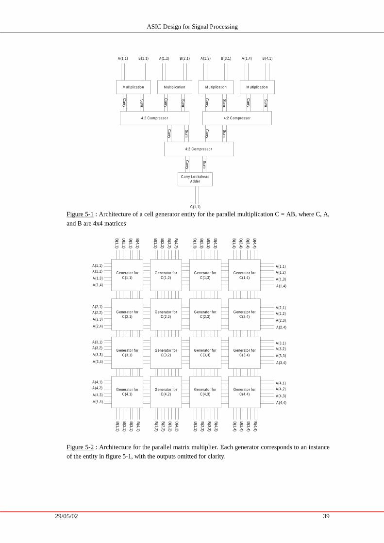
ASIC Design for Signal Processing
29/05/02 39
Figure 5-1 : Architecture of a cell generator entity for the parallel multiplication C = AB, where C, A,
and B are 4x4 matrices
Figure 5-2 : Architecture for the parallel matrix multiplier. Each generator corresponds to an instance
of the entity in figure 5-1, with the outputs omitted for clarity.
M ultiplicatio n M ultiplicatio n M ultiplicatio n M ultiplicatio n
A (1,1) B (1,1) A (1,2) B (2,1) A (1,3) B (3,1) A (1,4) B (4,1)
Carry
Sum
Carry
Sum
Carry
Sum
Carry
Sum
4:2 Co m presso r
Carry
Sum
4:2 Co m presso r
Carry
Sum
4:2 Co m presso r
Carry
Sum
Carry Lo o kaheadAdder
C(1,1)
B(1,1)
B(2,1)
B(3,1)
B(4,1)
G enerato r fo rC(1,1)
A (1,1)A (1,2)
A (1,3)
A (1,4)
A (2,1)
A (2,2)
A (2,3)
A (2,4)
A (3,1)
A (3,2)
A (3,3)
A (3,4)
A (4,1)
A (4,2)
A (4,3)
A (4,4)
G enerato r fo rC(4,1)
G enerato r fo rC(3,1)
G enerato r fo rC(2,1)
B(1,2)
B(2,2)
B(3,2)
B(4,2)
G enerato r fo rC(1,2)
G enerato r fo rC(4,2)
G enerato r fo rC(3,2)
G enerato r fo rC(2,2)
B(1,3)
B(2,3)
B(3,3)
B(4,3)
G enerato r fo rC(1,3)
G enerato r fo rC(4,3)
G enerato r fo rC(3,3)
G enerato r fo rC(2,3)
B(1,4)
B(2,4)
B(3,4)
B(4,4)
G enerato r fo rC(1,4)
G enerato r fo rC(4,4)
G enerato r fo rC(3,4)
G enerato r fo rC(2,4)
B(1,1)
B(2,1)
B(3,1)
B(4,1)
B(1,2)
B(2,2)
B(3,2)
B(4,2)
B(1,3)
B(2,3)
B(3,3)
B(4,3)
B(1,4)
B(2,4)
B(3,4)
B(4,4)
A(1,1)
A (1,2)
A (1,3)
A (1,4)
A (2,1)
A (2,2)
A (2,3)
A (2,4)
A (3,1)A (3,2)
A (3,3)
A (3,4)
A (4,1)
A (4,2)
A (4,3)
A (4,4)

ASIC Design for Signal Processing
29/05/02 40
5.2. Fully Sequential Matrix Multiplier
The fully sequential design contains a single multiplier, and hence must calculate each cell one
at a time. The consequence of this is that all of the results must be stored in some kind of
readable memory, and the design also needs to be synchronous.
This allows the use of pipelining in the design, which can significantly shorten the time required
by the matrix multiplication. Hence, the clock cycle length only needs to be as long as the
slowest pipeline stage, but several cycles are required for the entire operation. In summary, the
required stages are:
1. Read the data from memory. Two separate memories hold the two matrices, so
that they can both be read at once.
2. Wait for the data to arrive from the memory. This is required because the
memories that are to be used have clocked outputs, meaning that the read
address will be latched into the memory at the start of this stage, but the data
will not be latched to the output until the start of the next stage.
3. Perform the multiplication
4. Add the multiplication result to the tally
5. Resolve from carry-save into normal binary form
6. Write the result to memory
Combining stages could further optimise the design, but the specific nature of these adjustments
depends on the required implementation. Combining stages means that less pipeline registers
are required, and one clock cycle of operating time is saved for each stage that is merged.
However, one must be careful that the new combined stage does not have the longest delay over
any of the other stages, otherwise the clock cycle time may need to be increased.
In addition, the pipeline registers prevent the changing output signals of each stage from
reaching the next stage until they are at their final value. Removing a pipeline register between
two stages will not affect the accuracy of the result if the clock cycle is long enough, but it is
likely that the logic gates in the second stage will undergo more state transitions than
previously. The consequence of this is that the device may consume more power because, as
already outlined in chapter 2, logic gates that undergo a state transition consume more power
than gates which remain at a static level.
In summary, the advantages of this design are:
• There is only one multiplier, so comparatively small surface area required on the chip
• Inputs are only required one at a time, which could minimise complexities with routing
the input signals around the chip.

ASIC Design for Signal Processing
29/05/02 41
The main disadvantage is that a fully sequential matrix multiplier takes the most time to
complete its operation. Multiplying two 4x4 matrices would require at least 64 clock cycles. (16
cells x 4 multiplications for each)
5.3. Double Buffering Issues
One of the issues that has needed addressing in this project is the situation when the memory
which provides the input matrix is also the destination for the output matrix, such as the
calculation A = B*A. A simple approach is to simply use a double buffering approach where we
use a different memory for the output, effectively creating two different versions of A.
The double buffering technique may not always be a desirable approach:
• The additional memory requires surface area on the silicon chip
• In an implementation where the same matrix was used several times, logic would be
required to keep track of which version of A is the current one, and multiplexers would
be required to switch between the two.
By studying the ordering in which values are read and written, we can devise an alternative
approach. Considering the calculation C = AB,
• For each cell of C, we need to
o Read a row of cells from A
o Read a column of cells from B
• The most efficient method of generating C is to calculate each cell one at a time, either
working across the rows one at a time, or down the columns one at a time
• For each cell in a given column of C, we require the same column from B. That column
from B is not required for calculation of cells in any other column of C.
• For each cell in a given row of C, we require the same row from A. That row from A is
not required for calculation of cells in any other row of C.
Therefore,
• Once we have generated any given column of C, we no longer need the corresponding
column from B.
• Once we have generated any given row of C, we no longer need the corresponding row
from A.
This is illustrated in figure 5-3, for the case of generating columns of C at one time.

ASIC Design for Signal Processing
29/05/02 42
Figure 5-3 : Order in which rows and columns are read when the output matrix is written by working
down the columns. The output cells are in the same column of the output matrix as the cells that are
being read from the second input matrix. When the column of the output matrix is complete, we no
longer need the corresponding column from the input matrix.
The solution to the problem is then
• If C and A are the same, then for every row of C,
o Read in the appropriate row of A for the first cell in that row of C
o Latch it, and use the latched value for all other cells in that row of C
o The values that are output will go to the row of C/A that is latched, so the
original values can still be used for the time that they are needed.
• If C and B are the same, then for every column of C,
o Read in the appropriate column of B for the first cell in that column of C
o Latch it, and use the latched value for all other cells in that column of C
o The values that are output will go to the column of C/B that is latched, so the
original values can still be used for the time that they are needed.
However, only one of these solutions can be used at one time.
5.4. Semi Parallel / Semi Sequential Matrix Multipliers
Each of the cases described so far has a major disadvantage that prevents it being suitable for
use within this signal processor. The parallel architecture requires excessive surface area in
order to implement the required amount of the multipliers. The sequential design is efficient in
terms of surface area, but is too slow for the requirements of the signal processor. Hence, a
technique is required that uses a small amount of multipliers, but operates over a small enough
number of clock cycles.
X = X =
X = X =
X = X =
X = X =
1. 2. 3. 4.
5. 6. 7. 8.
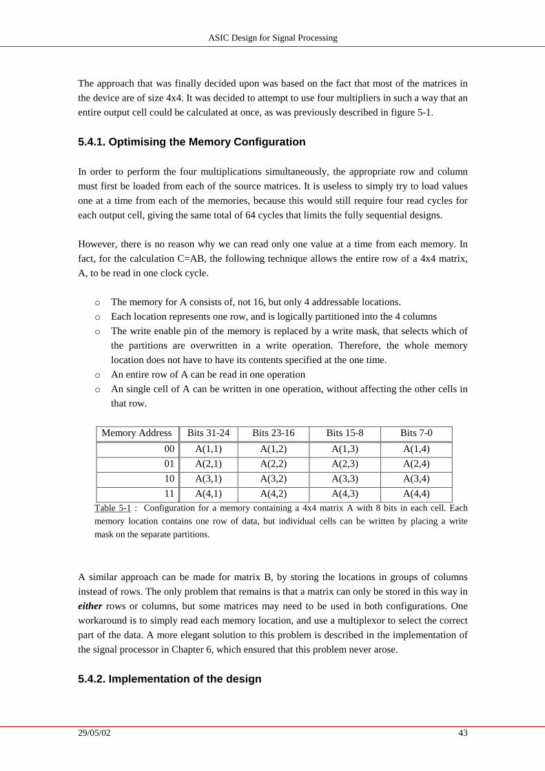
ASIC Design for Signal Processing
29/05/02 43
The approach that was finally decided upon was based on the fact that most of the matrices in
the device are of size 4x4. It was decided to attempt to use four multipliers in such a way that an
entire output cell could be calculated at once, as was previously described in figure 5-1.
5.4.1. Optimising the Memory Configuration
In order to perform the four multiplications simultaneously, the appropriate row and column
must first be loaded from each of the source matrices. It is useless to simply try to load values
one at a time from each of the memories, because this would still require four read cycles for
each output cell, giving the same total of 64 cycles that limits the fully sequential designs.
However, there is no reason why we can read only one value at a time from each memory. In
fact, for the calculation C=AB, the following technique allows the entire row of a 4x4 matrix,
A, to be read in one clock cycle.
o The memory for A consists of, not 16, but only 4 addressable locations.
o Each location represents one row, and is logically partitioned into the 4 columns
o The write enable pin of the memory is replaced by a write mask, that selects which of
the partitions are overwritten in a write operation. Therefore, the whole memory
location does not have to have its contents specified at the one time.
o An entire row of A can be read in one operation
o An single cell of A can be written in one operation, without affecting the other cells in
that row.
Memory Address Bits 31-24 Bits 23-16 Bits 15-8 Bits 7-0
00 A(1,1) A(1,2) A(1,3) A(1,4)
01 A(2,1) A(2,2) A(2,3) A(2,4)
10 A(3,1) A(3,2) A(3,3) A(3,4)
11 A(4,1) A(4,2) A(4,3) A(4,4) Table 5-1 : Configuration for a memory containing a 4x4 matrix A with 8 bits in each cell. Each
memory location contains one row of data, but individual cells can be written by placing a write
mask on the separate partitions.
A similar approach can be made for matrix B, by storing the locations in groups of columns
instead of rows. The only problem that remains is that a matrix can only be stored in this way in
either rows or columns, but some matrices may need to be used in both configurations. One
workaround is to simply read each memory location, and use a multiplexor to select the correct
part of the data. A more elegant solution to this problem is described in the implementation of
the signal processor in Chapter 6, which ensured that this problem never arose.
5.4.2. Implementation of the design

ASIC Design for Signal Processing
29/05/02 44
With these memory optimizations, it is possible to create a multiplier of two 4x4 matrices that
takes only 16 clock cycles, plus the additional cycles required to clear the pipeline. For the
operation C=AB, the pipeline stages are
1. Read a row from A, and a column from B
2. Delay so that data has time to arrive from the latched memory outputs
3. Perform the multiplications
4. Tally the multiplication outputs into two carry-save results
5. Resolve the carry-save results into a standard binary form
6. Output result to memory
As with the sequential design, if C is the same as A or B, then the appropriate row or column
may be latched when it is first read.
5.4.2.1 Non-conforming matrices If the memory locations representing the matrix B, in C=AB, do not contain columns of data,
then the data can be read as such:
o For each column of output cells,
o Read each cell for the appropriate column in B, simultaneously reading one of
the rows of A (4 read cycles)
o Store the column that has been read and perform the multiplications as normal
o Read each of the other three rows and perform the calculations for the
respective cells of C, using the remembered column (3 read cycles)
This technique requires only 7 reads per output column, giving a total of 7*4 columns=28
cycles for the operation, plus the time required to clear the pipeline.

ASIC Design for Signal Processing
29/05/02 45
5.4.2.2 One matrix doesn’t conform, and the other needs to be overwritten
One problem which arose with the original design was an equation of the form B = AB, where
both A and B needed to be stored in memory cells containing columns. It is wasteful to simply
store the answer in a different memory, and this can further complicate other parts of the design.
o For the problem of reading and writing the same matrix in the sequential design, we
would simply store the current column from B while we used its contents and overwrote
those values in the memory. We would write B by working down the columns,
remembering the column input from B and reading cells from each row of A as required
o For the problem of matrix A not conforming to containing a complete row in one
memory location, we decided to read in the row from A, and store it in a latch so that
we would not have to repeat those four read operations. We would then work across the
rows of the output matrix
Clearly there is a major clash in these two solutions – we cannot calculate the output matrix by
working across both the rows and the columns at the same time!
The most criti cal problem with B = AB is that the output is the same as one of its inputs, so this
must be addressed first. The issue of the cells of A being grouped in columns instead of rows
requires additional read cycles, but does not affect the output. The solution is then:
o Read the four locations in order to obtain the require row of A. At an appropriate time,
read in the column from B that is to be overwritten, and also read in the same column
from A. Store both columns, since the second matrix will be overwritten and we want to
save some read cycles from the first matrix. (4 read cycles)
o Perform the multipli cations as normal for that cell
o For the other cells in the same column of the output matrix, use the stored column of B.
For A, we have also stored one column, so we already know one value from the next
row. Read the other columns in order to obtain the rest of the row (three reads)
o After each set of 3 reads, perform the calculations as normal
This process is ill ustrated by figure 5-4.

ASIC Design for Signal Processing
29/05/02 46
Figure 5-4: Order in which matrix cells are read, for the calculation of the third column of the output
matrix, for the case where both matrices are stored with columns in each address. The cells of the
first row need to be read one at a time (a,b,d), but at an appropriate time we read and store the
required column for both matrices (c). For the rest of the cells in that output column, we then only
need to read the cells from the columns that were not stored (e,f,g for row 2, and h,i for row 3)
This gives a total of 4+3*3=13 read cycles for each column of the output matrix, with a total of
52 cycles to perform the entire operation. The time required is 1.85 times more than the 28
cycles that would be needed by doing the following, if space permitted:
o using an extra memory to eliminate the problem of reading and writing to the same
memory
o using the previously described solution to handle the fact that the contents of A are
stored in columns instead of rows.
X X X
X X X
X X X
a. b. c.
d. e. f.
g. h. i.

ASIC Design for Signal Processing
29/05/02 47
5.5. Squaring Matrices
A further problem is that fact that some of the multipli cations that are required involve the same
matrix on both inputs. While the solutions in section 5.4.2.1 ensure that we can work around the
problem of the matrix not conforming to both the row and columns format, it cannot deal with
the problem of needing to read two different memory addresses at the same time. One simple
approach may be to insert an extra read cycle into the pipeline, but it may not always be
desirable to increases the pipeline length in this way. Fortunately, even in the absence of dual
read port memories, there exists a solution that does not require additional clock cycles.
As an example, take the 4x4 matrix A, which is stored with an entire column in each memory
location. To perform the calculation of one output cell , we need to read an entire row and an
entire column, as depicted by figure 5-5.
Figure 5-5 : The row and column required for the calculation of a given output cell
Figure 5-6 demonstrates that, since that row and column are sourced from the same matrix, they
overlap by one cell:
Figure 5-6 : The row and column required from a single matrix that is to be squared, required to
calculate the output cell .
The required row can be read one cell at a time. However, since we actually need to read the
whole column in order to obtain that value, at some stage the entire column that is required will
also be read. In this way, we can obtain the column “ for free”, the same as if it had been read
from a separate memory.
Figure 5-7 : If the matrix of figure 5-5 is stored so that each address contains an entire column, then
to read the row we need to read each column at a time and extract the relevant data for the row. One
of these reads will also allow us to obtain the required column “ for free”.
Further optimizations may also be obtained by storing a row or column to prevent the need to
reread data, as described in section 5.4.2.1. The result is a squaring operation that can be
performed in the same amount of time as an equivalent two matrix multipli cation.
X =
2
=

ASIC Design for Signal Processing
29/05/02 48
5.6. Multiplying any combination of matrices
In summary, this chapter has described methods that would allow the multiplication of any
combination of matrices, as described by table 5-2. In all cases, the sources are 4x4 matrices,
but these methods could easily be adapted for any size, and not just square matrices. This
assumes that the matrices are stored with either entire rows, or entire columns, in each memory
address. For multiplications where there is one cell per memory address, see section 5.2.
Calculation Cycles Sections Comments
C = AB 16 5.4.2 A is stored with rows in each memory address, B with
columns in each memory address
C = AB 28 5.4.2.1 Both A and B are stored with rows in each memory address,
or with columns in each memory address.
B = AB 52 5.4.2.2 A and B are both stored with columns in each memory
address. The same method can be adapted for rows, by
latching the columns one cell at a time
A = AB 52 5.4.2.2 Same as B=AB, but the output is calculated by working
across the rows, rather than down the columns.
B = A2 52 5.5 A is stored with columns in each memory address, but the
same method can be adapted for if A contained rows in each
address.
A = A2 Not possible. The described method, for when the destination
is also one of the sources, is that we calculate the answer by
working across either rows or columns of the output, while
remembering the corresponding contents of the original.
Since squaring requires both rows and columns, this cannot
be done unless we use the form B = A2. Table 5-2 : Multiplications for 4x4 matrices can be done for almost any configuration. Where a letter
A or B appears twice in a single calculation, it is referring to the same matrix.

ASIC Design for Signal Processing
29/05/02 49
5.7. Testing and Verification
I have implemented and tested the three types of designs with a series of VHDL test benches:
• The first step was to verify the correct operation of the matrix multiplier logic, without
having to be concerned with the additional complication of memory accesses. To
achieve this, the test bench acted as a set of dummy memories that were guaranteed to
work. In addition, these multipli cations used only integers. The control logic of the
design was then the only component under test, as the multipliers were already
guaranteed to work and the requantisation logic was not used.
• Next, the requantisation logic needed to be tested, by using fixed point real numbers in
the tests.
• The final step was to build a realistic memory interface for the multiplier circuits, and
coordinate reads and writes between that, the test bench, and multiplier design. This
involved testing of both the interface, and the read/write logic of the multiplier design.
In order to test the correctness of the designs, a known accurate result was required. This was
obtained from a MATLAB script, which ran a random multipli cation of quantised matrices and
output the results to a file. The actual test bench consisted of a number of modes, each
performing a separate function:
1. Initiali se test bench and read data from the test file, including the number of
tests and configuration of the matrices. Change to mode 2 after 1 cycle
2. Read in all of the data from the test file for one test. This consists of the real
and imaginary parts of the input and output matrices. Change to mode 3 after 1
cycle
3. Initiali se the memories of the matrix multiplier. Write one address in each
matrix per cycle, and change to mode 4 when finished
4. Reset the matrix multiplier, telli ng it to start calculating. Change to mode 5
5. Wait one cycle for the multiplier’s signals to reach the test bench. Change to
mode 6
6. Wait until the multiplier’s “busy” signal becomes deasserted. When this occurs,
prepare the output memory for reading of the first value and change to mode 8
7. Read the data on the memory’s output line and store it in the test bench. If there
are more values left, then prepare the memory for the next read and change to
mode 8, otherwise change to mode 9.
8. Wait for a cycle while the data is read from the memory and becomes latched to
its outputs. Change to more 7
9. Compare the data read from the output memory with the answer read from the
test file. If they differ, generate a failure message. If there are more tests left,
then go to mode 2.

ASIC Design for Signal Processing
29/05/02 50
6. Implementation of the Signal Processor
In order to implement the algorithm, the signal processor needs to perform the following
additional types of operations:
• A multiplication A = B * B*, where B is a 4 x 128 matrix
• A number of multiplications of pairs 4x4 Hermitian matrices, of the configuration types
that were covered in Chapter 5.
• A multiplication of a 4x4 Hermitian matrix by a 4x1 matrix
The matrix multiplier that was chosen to form the core of the design is the semi-parallel
architecture described in section 5.4. Only the final design, which takes advantage of the
Hermitian properties, is described here, but an earlier version for general matrix multiplications
was also built on the same principles and techniques outlines in chapter 5.
The challenge that forms the key part of the architecture was to solve the following
complications:
1. There is only enough physical space to implement the one matrix multiplier. This means
that as much of the architecture as possible must be common for each multiplication
that is to be performed
2. Some matrices appear as the first term in some multiplications, and the second term in
others. Since the matrices can only be stored as either columns or rows, and not both,
this means that these matrices will be in the wrong form for some of the calculations.
3. The results of the matrix multiplications must be Hermitian when required. As already
discussed in section 3.1.2, the simple cropping techniques that are used in hardware do
not allow this.
The first problem is simply a design constraint that needs to be adhered to when addressing the
other issues, while the third problem is the easiest to solve.

ASIC Design for Signal Processing
29/05/02 51
6.1. Ensuring that the output matrices are Hermitian
The approach to the solution of this problem has already been specified by the fixed point
MATLAB model, which is to calculate the top diagonal half of the matrix, and guess the other
half. It is necessary to follow exactly the same approach so that the two models may be checked
for accuracy.
On this occasion, the design specifications work in favour of the problem, providing a simple
method of implementation. The key is in how the matrix cells are addressed, ill ustrated in figure
6-1.
0000 0001 0010 0011
0100 0101 0110 0111
1000 1001 1010 1011
1100 1101 1110 1111
Figure 6-1 : Memory addresses for the cells in a 4x4 matrix, in binary form
Each output matrix is of size 4x4, and each cell i s given a four bit address. The least significant
2 bits correspond to the physical memory address that is used to store the value, and the most
significant two bits match the partition number within the memory write mask.
Table 6-1 : Mapping of logical memory addresses to positions within the physical memory locations.
The trick to writing Hermitian matrices is to notice the similarity between the addresses of cells
that are mirrored across the main diagonal. Such pairs of cells are 0100 and 0001, 1001 and
0110, 1000 and 0010, etc. In all cases, if the least significant two bits are swapped with the most
significant two bits, then the address of that cell ’ s partner is formed.
Therefore, the algorithm for writing these matrices is simple:
o Write the cell i n the top half of the matrix with the calculated value
o Swap the two halves of the address, and take the conjugate of the calculated value.
o Write the new value to the modified address.
The problem which this leaves is that only one write can be done per clock cycle, so this needs
to be considered in the rest of the design. However, the need to wait for an extra clock cycle
also gives the circuit time to form the conjugate of the original calculation.
Physical Address
Bits 31-24
Bits 23-16
Bits 15-8
Bits 7-0
00 1100 1000 0100 0000 01 1101 1001 0101 0001 10 1110 1010 0110 0010 11 1111 1011 0111 0011

ASIC Design for Signal Processing
29/05/02 52
6.2. Taking Advantage of Hermitian Matrices
A further property of the algorithm’s matrices allows a simpli fication that solves the second of
the design problems. If it can be assured, by section 6.1, that the input matrices are Hermitian,
then they will be of the following form:
A B C D
/B E F G
/C /F H I
/D /G /I J
Figure 6-2 : Form of the 4x4 Hermitian matrix. “ /B” means “conjugate of B”
The key observation is that for any row n, the corresponding column n contains the conjugates
of the same values. The diagonal contains entirely real numbers, which are conjugates of
themselves.
In addition, the complex multiplier has already been designed to allow multipli cation by the
conjugate of its inputs, to cater for the calculation of A*A*. This provides the necessary
components to implement the following simple solution:
o Implement all matrices by storing them in the form of one column within each memory
address.
o When a column is needed, simply read the appropriate address
o When a row is needed, read the address of the corresponding column, and set the
multiplier to use the conjugate of its input value.
This solution further simpli fies the hardware implementation due to the fact that every matrix
multipli cation requires the reading of rows from one of the matrices. Therefore, the multipliers
will always be taking the conjugate of one of the inputs, and the signal that controls this
function will be constantly asserted. The synthesis tool will recognise this, and optimise the
circuit to remove the redundant case.

ASIC Design for Signal Processing
29/05/02 53
6.3. Performing multiplications with Hermitian optimisations
Using the technique described in section 6.1, when we calculate any non-diagonal cell of the
output matrix the conjugate value is also written to its corresponding cell on the other side of the
diagonal. Therefore, once the first row of the output matrix has been calculated, the first column
has also been assigned new values. The next cell to be calculated is then in the second row and
the second column. This pattern continues, and the output matrix is completed in the manner
depicted by figure 6-3.
Figure 6-3 : Order in which the Hermitian matrices are fill ed in. Dark squares represent the cells
currently being written, and light squares represent the cells already calculated.
This information is helpful for performing the squaring of Hermitian matrices. Since the rows
and columns come from the same matrix, it may first appear that it is necessary to perform two
reads per output cell . However, on closer inspection, that is not necessary.
The key observation in figure 6-3 is that the first cell to be explicitl y written on each row of the
output matrix lies on the diagonal. That means that the row and column required for that
calculation have the same memory address. For the matrix squaring, by section 6.2, the first
location read for each output row contains both the data for the row to be read, and the column
required for the first calculation. All that is required is to store that row’s data, and for the other
output cells in that row, read each column as required and use the stored row.
For general Hermitian matrix multipli cations, exactly the same technique can be used. Although
it is not necessary to remember the row data in this case, it is more consistent to do so and
allows for simpler circuitry.
6.3.1. Multiplication of any Hermitian matrices
The technique described in this section allows for the calculation of any of the cases from table
5-2 in 16 cycles, when all of the source matrices are known to be Hermitian. When one, or none
of the source matrices are Hermitian, then the techniques described in section 5.6 may be used.
Hence, we now have a way for multipli cation of almost any combination of valid matrices, so
the next step was to build the signal processor that demonstrated an implementation of this
theory.

ASIC Design for Signal Processing
29/05/02 54
6.4. Signal Processor Architecture
Once the design problems had been resolved, it was possible to fully develop the processor data
path and control sequence. The concept behind how each type of multiplication works is the
same, and the general sequence of events for the generation of each matrix cell is summarised in
figure 6-4.
Figure 6-4 : The four stages required for performing matrix multiplication. Each piece of data read
from the memories passes through each stage, and these stages can be pipelined to improve the
circuit performance.
The system can be divided into four pipeline stages, providing the following functionality:
1. The Read stage generates the address of the row or column that is to be read from
each matrix, and the address of the cell that will be written to the output matrix with
the results of this newly addressed data.
2. The delay stage waits for the data to become available from the memories
3. The Multiplication stage performs the four multiplications, and tallies the results
together in carry-save format.
4. Finally, the results are resolved into standard binary form and written to the
destination memory.
Several of the original stages described in the semi-parallel architecture have been merged in the
final design, mainly because propagation delay was not an issue. One reason for this is that the
merged stages easily fit within the specified 8ns clock cycle time. Another advantage is that
reducing the number of clock cycles between the read and write stages removes complications
with timing synchronisation and read-after-write dependencies.
An overview of the processor architecture is provided by figure 6-5. The control unit, as
described within this chapter, generates one set of addresses and data, which is sent to each of
the memories. The data read from each of the memories is fed into multiplexors, to select which
pieces of data are currently required by the controller. A separate set of signals is used for the
special mode 0 memory, which is of a different size to the others.
Stage 2:
W ait for data tobe read from
memories
Stage 1:
G enerate readaddresses for
memories
Stage 3:
PerformM ultip lications
Stage 4:
Add results tota lly and/or output
to ta l to m em ory
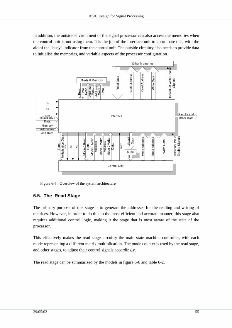
ASIC Design for Signal Processing
29/05/02 55
In addition, the outside environment of the signal processor can also access the memories when
the control unit is not using them. It is the job of the interface unit to coordinate this, with the
aid of the “busy” indicator from the control unit. The outside circuitry also needs to provide data
to initiali se the memories, and variable aspects of the processor configuration.
Figure 6-5 : Overview of the system architecture
6.5. The Read Stage The primary purpose of this stage is to generate the addresses for the reading and writing of
matrices. However, in order to do this in the most eff icient and accurate manner, this stage also
requires additional control logic, making it the stage that is most aware of the state of the
processor.
This effectively makes the read stage circuitry the main state machine controller, with each
mode representing a different matrix multipli cation. The mode counter is used by the read stage,
and other stages, to adjust their control signals accordingly.
The read stage can be summarised by the models in figure 6-6 and table 6-2.
M UX
M o de 0 M emory
Co ntro l Unit
Interface
Rea
dA
ddre
ssW
rite
Add
ress
Writ
eD
ata
Rea
dD
ata
Other M emories
Rea
d A
ddre
ss
Writ
e A
ddre
ss
Writ
e D
ata
Rea
d D
ata
Indi
vidu
al W
rite
Ena
ble
Sig
nals
Rea
dD
ata
Writ
e A
ddre
ss
Rea
d A
ddre
ss
Writ
e D
ata
Indi
vidu
al W
rite
Ena
ble
Sig
nals
Mod
e 0
Rea
dA
ddre
ss
Mod
e 0
Writ
eA
ddre
ssM
ode
0 W
rite
Dat
a
Mod
e 0
Rea
dD
ataC
lk
Rst
Start
InitialisationData
C lk
Rst
S ta rt
M emoryAddressesand Data
Results andOther Data
Som
eIn
itial
isat
ion
Dat
a
BU
SY

ASIC Design for Signal Processing
29/05/02 56
Figure 6-6 : Conceptual view of the pipeline read stage. Numbers in parentheses represent the bus
size, while others are one bit signals.
Signal Type Description Clk Input 8ns system clock signal Rst Input When set low, resets the processor Restart Input When asserted high on a rising clock edge, signals the processor to
begin calculating the equation, using the current input values. Running Input Signal which indicates whether or not the processor should be doing
anything. If low, everything is disabled. Mode0_address1 Internal First address to read for a calculation in mode 0 Mode0_address2 Internal Second address to read for a calculation in mode 0 Mode0_read_Address Output Address to be read from memory on next clock cycle Int_out_addr Output Address of the output matrix cell which is to be calculated from the
data that is currently being addressed. Diagonal Output If high, then the cell addressed by int_out_addr is one the diagonal of
the output matrix. Do_wrt Output If high then, when the data which was addressed in the previous clock
cycle reaches the output stage, the result is to be written to memory. Mode Output The mode of the state machine. Allows control of multiplexors to
correctly direct data to/from memories. Mode0_counter Output Used for when stage 0 needs to read two addresses for each set of data,
by counting how many reads have been done. Read_delay Internal When low, stalls the pipeline for one cycle. This is because the output
stage sometimes requires two clock cycles, to write to both halves of the Hermitian matrix.
Mode0_delayed Internal Similar to read_delay, but specific to mode 0 Table 6-2 : Summary of signals for pipeline read stage.
The read addresses for memories, other than those used by mode 0, can be obtained directly
from the output address, since the row and column required for reading correspond directly to
the row and column of the cell that is to be written:
For example, Cell to be written : 0111
Row to be read : 01
Column to be written : 11
Clk
Rst
Restart
Running
Mode0_read_address (7)
Diagonal
Do_wrt
Int_out_addr (4)
Delay_running
Read Stage
Mode
Mode0_counter

ASIC Design for Signal Processing
29/05/02 57
6.5.1. Mode 0 – Calculating A = B * B*
The distinguishing features about mode 0 is that
o The input matrix is not square. For this analysis, it is considered to be 4x128, but the
width could be any power of two that is larger than 4.
o The multipli cation is of the matrix B, with the conjugate transpose of itself
In order to perform a matrix multipli cation of this type, we need to read a row and a column as
normal. The difference is that there are more than four multipli cations necessary for the
calculation of each output cell . In fact, the exact number will be the width of the input matrix B,
which is a multiple of 4 if the above constraints are met.
For the 4x128 matrix, this will require 128 multipli cations to obtain each output cell , using only
the 4 available multipliers. It is therefore clear that, for each output cell , 32 sets of 4 values must
be read, multiplied, and talli ed. When all 32 sets of data have been processed, the result can be
written to the output memory and the tally is cleared. The nature of this arrangement means that
it is best to structure the memory so that each address contains four values that are adjacent in
the same row of the matrix. Part of this matrix is shown in Figure 6-7
1 2 3 4 5 6 7 8 9 10 11 12 13 14 15 16
1 0000000 0000001 0000010 0000011
2 0100000 0100001 0100010 0100011
3 1000000 1000001 1000010 1000011
4 1100000 1100001 1100010 1100011 Figure 6-7 : Depiction of the 16 leftmost columns of a 4x128 matrix, and the memory locations
which contain their values.
However, there is a further complication. The problem is that the columns from the “second”
matrix of the multipli cation are really rows from the same matrix that is acting as the “first”
matrix of the multipli cation. Since the widths are much larger than four, it is not feasible to use
the techniques of remembering previously read data, that has been previously described. The
only practical solution is to alternately read data from the two different rows. Table 6-3
ill ustrates this process for calculating the output cell i n the first row and third column of the
output matrix.
Clock Cycle +0 +1 +2 +3 +4 +5 … +60 +61 +62 +63
Mode0_address1 0 1 2 … 30 31
Mode0_address2 64 65 66 … 94 95
Mode0_read_address 0 64 1 65 2 66 … 30 94 31 95
Mode0_counter 0 1 0 1 0 1 … 0 1 0 1
Do_wrt 1 0 0 0 0 0 …. 0 0 0 0 Table 6-3: Signal values for multiplication involving two different rows of the input matrix

ASIC Design for Signal Processing
29/05/02 58
However, for output cells on the diagonal, the two sets of rows that are read are the same.
Therefore, as shown in table 6-4, there is no need to waste clock cycles by performing two reads
for each pair of four values.
Clock cycle +0 +1 +2 +3 … +29 +30 +31
Mode0_address1 32 33 34 35 … 61 62 63
Mode0_address2 32 33 34 35 … 61 62 63
Mode0_read_address 32 33 34 35 … 61 62 63
Mode0_counter 0 0 0 0 … 0 0 0
Do_wrt 1* 0 0 0 … 0 0 0 Table 6-4 : Signal values for multiplications involving one row of the input matrix. * : For the first
row, Do_wrt is initially low because that is the first calculation of the mode.
It is also convenient that the cells which only require one read for each pair of four values, the
diagonals, are also the ones which only require one write cycle. This makes some calculations
take more cycles than others, but no pipeline delays are required because there is at least a 31
cycle delay between writes, and the output stage is the only stage that would be affected by this
situation. The next mode is not affected either, because the final cell only requires a single write
cycle.
Using this information, we can calculate how many cycles are required for each stage of the
operations. Table 6-5 ill ustrates the start cycle of the calculation of each of the output values,
after which the signals take on one values in one of the above tables, as appropriate.
Clock Cycle 0 32 96 160 224 256 320 384 416 480 512
Mode0_address1 0 32 64 96 32 64 96 64 96 96 next
Mode0_address2 0 0 0 0 32 32 32 64 64 96 mode
Mode0_base1 0 0 0 0 32 32 32 64 64 96
Diagonal 1 0 0 0 1 0 0 1 0 1 1 Table 6-5 : Signal values for the first clock cycle of the start of the calculation of each output cell .

ASIC Design for Signal Processing
29/05/02 59
6.5.2. Final Mode : Multiplying a 4x4 matrix by a 4x1 matrix
This mode involves the multiplication of the matrix stored in one of the memories, by a 4x1
matrix that is latched in from the inputs at the start of the calculation of the output matrix. The
output matrix is a 4x1 matrix, so each column of the 4x4 input only needs to be read once.
Clock Cycle 0 1 2 3 4
Int_out_addr 0000 0100 1000 1100 next
Diagonal 1 1 1 1 mode Table 6-6 : Signal values for the first clock cycle of the start of the calculation of each output cell.
The memory read addresses are obtained directly from the int_out_addr signal, as previously
described.
6.5.3. Other modes : Multiplying two 4x4 matrices
All of the other modes involve multiplying together two 4x4 Hermitian matrices, which can be
achieved using the principles described in sections 5.4.2.1, 5.5, and 6.2. The timing of the read
cycle then becomes as shown in table 6-7.
Clock Cycle 0 1 2 3 4 5 6 7
Int_out_addr 0000 0001 0001 0010 0010 0011 0011 0101
Read_delay 1 0 1 0 1 0 1 1
Diagonal 1 0 0 0 0 0 0 1
Clock Cycle 8 9 10 11 12 13 14 15 16
Int_out_addr 0110 0110 0111 0111 1010 1011 1011 1111 next
Read_delay 1 0 1 0 1 0 1 1 mode
Diagonal 0 0 0 0 1 0 0 1
Table 6-7 : Signal values for the first clock cycle of the start of the calculation of each output cell.
The memory read addresses are obtained directly from the int_out_addr signal, as previously
described.
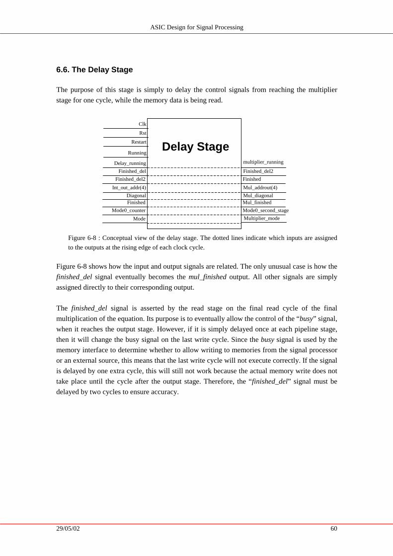
ASIC Design for Signal Processing
29/05/02 60
6.6. The Delay Stage The purpose of this stage is simply to delay the control signals from reaching the multiplier
stage for one cycle, while the memory data is being read.
Figure 6-8 : Conceptual view of the delay stage. The dotted lines indicate which inputs are assigned
to the outputs at the rising edge of each clock cycle.
Figure 6-8 shows how the input and output signals are related. The only unusual case is how the
finished_del signal eventually becomes the mul_finished output. All other signals are simply
assigned directly to their corresponding output.
The finished_del signal is asserted by the read stage on the final read cycle of the final
multipli cation of the equation. Its purpose is to eventually allow the control of the “busy” signal,
when it reaches the output stage. However, if it is simply delayed once at each pipeline stage,
then it will change the busy signal on the last write cycle. Since the busy signal is used by the
memory interface to determine whether to allow writing to memories from the signal processor
or an external source, this means that the last write cycle will not execute correctly. If the signal
is delayed by one extra cycle, this will still not work because the actual memory write does not
take place until the cycle after the output stage. Therefore, the “finished_del” signal must be
delayed by two cycles to ensure accuracy.
Clk
Rst
Restart
Running Delay Stage
Delay_running
Finished_del
Finished_del2
Int_out_addr(4)
Diagonal Finished
Mode0_counter
Finished_del2
Finished
Mul_addrout(4)
Mul_diagonal Mul_finished
Mode0_second_stage
multiplier_running
Mode Multiplier_mode

ASIC Design for Signal Processing
29/05/02 61
6.7. The Multiplication Stage The multiplication stage receives four pairs of numbers from the memories, multiplies them,
and adds the results together to form the value for the appropriate output cell. For mode 0, there
are more than four multiplications to be done, so the result must be added to a tally by the
output stage until all values have been calculated.
Figure 6-9 : Conceptual View of the multiplication pipeline stage.
Most of the input signals come from either the delay stage, or are global control signals (clk, rst,
restart, and running) The only exceptions are
• The data that is read from the memories, after being addressed by the read stage
• The do_wrt signal. This signal indicates whether the results of the multiplication stage
are to be written to memory, or tallied for later use. For simplicity of code, it is
generated by the read stage at the start of the calculation of the next result. Hence, it is
generated a cycle later than required, and bypasses the delay stage in order to regain
synchronisation.
Most of the output signals are simply copies of the input signals, as indicated by figure 6-8. The
only thing that is generated by this stage is the results of the multiplication.
Data from memories
Clk
Rst
Restart
Running
Multiplication Stage
multiplier_running
Mul_addrout(4)
Mul_diagonal Mul_Finished
Mode0_second_stage
Comb_addrout(4)
comb_diagonal comb_finished
output_running
Multiplier_Mode comb_mode
Chanel_mask
Do_wrt
Results of multiplication
comb_wrt comb_twowrites

ASIC Design for Signal Processing
29/05/02 62
6.7.1. Mode 0 – Calculating A = B * B*
The main difference of this mode from others is that there is the situation where two reads need
to be done before the multipli cation can take place. The mechanism for coping with this is
simple:
• On the first cycle, store the data in a register
• On the second cycle retrieve that data and use it as one of the inputs to each multiplier.
The other inputs come directly from the memory data that was just read.
For the case where only one read is required, we can simply direct the data read from the
memory to both multiplier inputs. This works because the multipliers are set up to automatically
take the conjugate of the second input, so no further manipulation is required. Appendix B2.2.1,
and figure 6-10, summarise this process.
Figure 6-10: Data path for multiplication mode 0. Where we require data from two different rows of
the input matrix, it is stored in the register on the first read, for use in the multiplier when data is
available from the second read. Where both pieces of data come from the same row (i.e. the same
piece of data), both value are taken directly from the incoming data stream.
6.7.2. Other Modes
The technique used to perform these multipli cations has already been outlined in section 6.3,
and this is fairly simple to implement:
• If the output cell being calculated is on the diagonal, then read both multiplier inputs
from memory and store the row for later use.
• Otherwise, use the remembered row as one input, and read the column from the
appropriate memory.
• For the multipli cation by a 4x1 matrix, we do not use the stored the row but read it from
memory. The column is read from a latched direct input.
In the above, a “row” is actually a column of the Hermitian matrix, of which the conjugate is
taken. The flowchart for this mode is provided in Appendix B2.2.2
a x bb
aX
Zb
a2:1
da ta
resu lt
R eg is te r

ASIC Design for Signal Processing
29/05/02 63
6.8. The Recombine and Output Stage The final stage in the pipeline, presented in figure 6-11, involves converting the carry-save
components into standard binary numbers.
Figure 6-11: Conceptual view of the output pipeline stage.
Details of the implementation are ill ustrated in Appendix B5.
6.8.1. Clamping overflowed values
When a multipli cation between two signed 16 bit numbers occurs, the result is a 31 bit value.
That is, twice the number of integer bits, twice the number of fractional bits, and one sign bit.
However, numbers of this size are too big to be stored in the memories, and so they must be
cropped in some way. Furthermore, since some of the results are to be reused in the
calculations, they need to be cropped so that they keep the original number of fractional and
integer bits.
The fractional bits can simply be cropped, with no further processing necessary. However, this
is not the case with the integer bits. In particular, we need to deal with the case where the value
of the result is outside of the allowed range.
For example, consider an 8 bit integer result, with an allowed range of ±16. That range consists
of the least significant 5 bits, so designate the 5th least significant bit as the “cropped sign bit” .
Now consider four examples:
5 : 00000101 17 : 00001011
-5 : 11111011 -17 : 11110101
Output to memory
Addr_out
Clk
Rst
Restart
Running
Recombine and Output
Stage
Comb_addrout(4)
comb_diagonal comb_finished
output_running
comb_mode
Results of multiplication
comb_wrt comb_twowrites
wrt

ASIC Design for Signal Processing
29/05/02 64
The examples 5 and –5 are within the allowed range, while 17 and –17 are not. Examination of
the binary encoding of these numbers will reveal that, for the numbers within the allowed range,
all of the bits from the cropped sign bit to the original sign bit are the same. This is not the case
for numbers that are not within range. Hence, we have a mechanism for detecting range
overflows.
The technique for clamping is then:
• Check if all of the bits above the clamping point are the same
• If they are, simply crop the number
• If not,
o Set the sign bit of the cropped number to the original sign bit
o Set all of the other bits to the inverse of the sign bit.
This will t hen ensure that and out of range numbers will be cropped to their upper or lower
extreme, as appropriate.
6.9. Disabling parts of the matrices
An extension to the design was to consider ways of “disabling” certain rows and columns of the
matrix, so that the 4x4 matrices would behave li ke 3x3, or 2x2 matrices. The disabled rows and
columns would simply contain zeroes. This proved to be a simple matter of:
• Disabling the appropriate multiplier. Due to the technique of reading in columns or
rows at a time, it happens that each multiplier always operates on data from the same
row or column. (The only exception is for mode 0.)
• Initiali se the appropriate rows or columns to zero at the start of the algorithm.
The result is that the matrices behave as if the disabled sections were not present. Furthermore,
the power consumption will also approach the levels as if the disabled sections were missing,
since the disabled multiplier saves power by preventing any glitches from propagating through
it. The calculation will still use the same number of clock cycles, but this is not an issue for this
design.
6.10. Testing and verification The testing of the final design made use of test benches that were heavily based on those used
for the matrix multiplier designs. Similar testing steps were followed, but were modified as
required to suit the algorithm. The only additional steps were to vary the various model
parameters, such as quantisation bits and range, to ensure that the design would match the
MATLAB model for all combinations.

ASIC Design for Signal Processing
29/05/02 65
6.11. Synthesis of Final Design
Synthesis of the signal processor was performed using the Synopsys software, since the
Cadence PKS license was not available for the time that it would be required. Since this
software is not believed have as accurate timing as Cadence PKS, the initial target was set to
7ns clock cycles. This was to ensure that the design would comfortably meet the timing
requirements of 8.2ns. A summary of results is given in table 6-8.
Timing Target
(ns)
Required Time (ns) Worst Path time (ns) Size (mm2)
7 6.61 6.62 2.45
8.2 7.72 7.71 2.00
Table 6-8 : Synthesis results for the signal processor, using Synopsys software.
Although the result for the 7ns target is reported as having violated the timing constraint (6.62 >
6.61), this is not a concern because it is merely the result of rounding errors and significant
digits. Simply reducing the target further would allow the worst path to fit within 6.61ns.
The size is an indicator of the physical space that the circuit would require on a silicon chip, and
includes the four 20x20 bit multipliers, the memories, and the control logic. As the results
indicate, the synthesis tool will attempt to optimise the circuit to provide a trade-off between
size and speed. As the timing constraint is relaxed to 8.2ns, it is able to reduce the size by using
slower, but more compact, logic.
6.11.1. Changes to described design
The initial synthesis indicated that the design may not quite fit within the design constraints, or
would at least be uncomfortably close to exceeding them. Analysis of the synthesis data
revealed that the worst path was through the multipliers, so this was the stage that had to be
modified.
A simple solution was applied, involving splitting this stage into two pipeline stages. The work
involved was simply the addition of a pipeline register in the manner that was described for the
delay stage. For the purposes of this thesis, it is more intuitive to describe these two stages as
one block. However, further splitting of pipeline stages would introduce read-after-write
hazards, and would be a more complicated process.

ASIC Design for Signal Processing
29/05/02 66
7. Conclusions and Extensions
This project has involved the implementation of a signal processing algorithm in a VHDL
model, which successfully matches the output of a corresponding MATLAB model with the
same quantisation configuration. This thesis has generalised the algorithm by describing a set of
techniques that can be applied to multiply almost any configuration of matrices, whether they
are Hermitian or not. A subset of these techniques was required for the signal processor,
demonstrating the practicality of implementation.
In particular, steps that I have completed to achieve this goal included:
• Research, design, implementation, and testing of high speed architectures for the
digital multiplication of numbers. This work is the only part which had been done
prior to the commencement of the project.
• Enhancing these multipliers with power saving optimisations, that disable the
multiplier circuit without increasing the critical delay. This technique has since been
filed for patent by Lucent Technologies.
• Research into alternative methods for implementing complex number multipliers
• Design, implementation, and testing of a complex number multiplier design
• Research, design, implementation, and testing of various architectures for the
multiplication of matrices, as described by chapter 5. Consequently, I have devised
methods for hardware multiplication of various combinations of matrices, as
summarised in 5.6 and 6.3.1
• Conversion of a floating point MATLAB model of the algorithm into a fixed point
quantised model, which emulates the desired performance of a hardware
implementation. This includes analysing the effects of adjusting the various model
parameters, and selecting the most appropriate combination.
• Incorporating the most appropriate matrix multiplier design into a control unit, to
produce the signal processor detailed by chapter 6.
All stages of the hardware implementations additionally required:
• Design of testing mechanisms to verify the correctness of the implementations
• Synthesis of the designs, and analysis of these results to determine the best way in
which to arrange the code.
• All of the multipliers have been written in a form that makes them generically sizable to
any width of input.

ASIC Design for Signal Processing
29/05/02 67
The result is a signal processor that performs the required calculations, meeting the following
specifications:
• It operates within 8ns clock cycles
• By use of optimisations specific to Hermitian matrices, the result is calculated in the
least number of cycles possible. This time is limited only by the number of reads and
writes that are required.
• It saves power, by performing as few calculations as needed. This includes taking the
conjugate of already calculated results (section 6.1) for the output matrices, and the
disabling of multipliers that are not in use (section 6.9).
• An appropriate amount of quantisation has been chosen to balance the physical size
with performance of the design.
7.1. Possible Extensions
This project has been built for a specific purpose, so all of the foreseen requirements of the
design have already been fulfill ed. Furthermore, I believe that the number of clock cycles
required for the algorithm is almost, if not exactly, minimal for the design constraints that have
been set. Therefore, any further extension to this project would involve only optimisation of the
various components of the design.
One obvious area would be further optimisation of the multiplier circuit, and this is an area that
is under constant research. The designs described in this document have been built for synthesis
by a tool such as Cadence PKS and Synopsys. However, experimentation by staff at Bell Labs
Research has shown that a “full -custom” design of the circuit and associated layout on the chip
has the potential to offer significant savings in surface area and speed.
One possibilit y could then be the generation of custom multipliers in much the same way as the
Artisan Components tool generates the memories used by this project. This would then allow
for the use of larger word widths in the processor, generating a better quality of result.
Furthermore, it would also allow the implementation of other architecture of multiplier, which
failed to produce their claimed benefits under normal synthesis.
In a similar way, other components of the design could also be optimised, but overall there is
littl e scope for extension to this project.

ASIC Design for Signal Processing
29/05/02 68
References
[1] http://mathworld.wolfram.com/ComplexNumber.html
[2] http://mathworld.wolfram.com/Matrix.html
[3] http://mathworld.wolfram.com/MatrixMultipli cation.html
[4] http://mathworld.wolfram.com/Transpose.html
[5] http://mathworld.wolfram.com/AdjointMatrix.html
[6] http://mathworld.wolfram.com/TraceMatrix.html
[7] http://mathworld.wolfram.com/HermitianMatrix.html
[8] Howard Anton & Chris Rorres, Elementary Linear Algebra Applications Version, John
Wiley & Sons Inc., 1994, 7th Edition, pp559-562,
[9] Douglas J. Smith, HDL Chip Design, Madison, AL, USA: Doone Publications, 1996, pp3-5
[10] Behrooz Parhami, “Computer Arithmetic” , Oxford Press, 2000, pp131
[11] Weste, Neil H.E. and Eshraghian, Kamran, Principles of CMOS VLSI Design: A systems
perspective, Addison-Wesley Publishing Company, 2nd ed., 1993, pp547-555.
[12] G. Knagge, “High Speed Multiplier Architectures” ,
http://geoffknagge.com/fyp/info.shtml#dl
[13] Y. B. Mahdy, S. A. Ali , K. M. Shaaban, “Algorithm and Two Eff icient Implementations
for Complex Multiplier” , Proceedings of ICECS ’99, vol 2, 1999, pp949-952
[14] Kyung-Wook Shin; Bang-Sup Song, “A complex multiplier architecture based on
redundant binary arithmetic”, Proceedings of 1997 IEEE International Symposium on
Circuits and Systems. Circuits and Systems in the Information Age. ISCAS 97, pp 1944-
1947.
[15] Yun Kim, Bang-Sup Song, John Grosspietsch, Steven F. Gilli g, “A carry-free 54b x 54b
Multiplier Using Equivalent Bit Conversion Algorithm”, IEEE Journal of Solid State
Circuits, Vol 36, No. 10, October 2001, pp1538
[16] Ravi K. Kolagotla, Hosahalli R. Srinivas, Geoffrey F. Burns, “VLSI Implementation of a
200-MHz 16x16 Left-to-Right Carry-Free Multiplier in 0.35µm CMOS Technology for
next-generation DSPs” , Proceedings of the IEEE Custom Integrated Circuits Conference,
1997, pp469-472
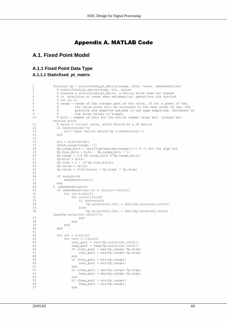
ASIC Design for Signal Processing
29/05/02 69
$SSHQGL � $� 0$7/��� �
RGH
A.1. Fixed Point Model
A.1.1 Fixed Point Data Type A.1.1.1 Staticfixed_pt_matrix 1 function fp = staticfixed_pt_matrix(range, bits, va lue, makeHermitian) 2 % staticfixed_pt_matix(range, bit, value) 3 % creates a staticfixed_pt_matix, a matrix which does not change 4 % in precision or range when mathematical operations are carried 5 % out on it. 6 % range = range of the integer part of the value. If not a power of two, 7 % the value given will be increased to the next power of two. The 8 % positive and negative extreme is the same magnitude, whichever of 9 % the given values is bigger. 10 % bits = number of bits fo r the entire number (sign bit, integer bit,
faction bits) 11 % value = initial value, which should be a 2D matrix 12 if ndims(value)~=2 13 err('input matrix should be 2 - dimensional'); 14 end 15 16 siz = size(value); 17 check_range(range,''); 18 fp.range_bits = ceil(log2(max(abs(range)))); % - 1 for the sign bit 19 fp.frac_bits = bits - fp.range_bits - 1; 20 fp.range = [ - 2^fp.range_bits 2^fp.range_bits]; 21 fp.bits = bits; 22 fp.step = 1 / (2^fp.frac_bits); 23 fp.value = value; 24 fp.value = floor(value / fp.step) * f p.step; 25 26 if (nargin<4) 27 makeHermitian=1; 28 end 29 % makeHermitian=0; 30 if (makeHermitian==1) & (siz(1)==siz(2)) 31 for cnt=1:siz(1) 32 for cnt2=1:siz(2) 33 if (cnt==cnt2) 34 fp.value(cnt2,cnt) = real(fp.value(cnt, cnt2)); 35 else 36 fp.value(cnt2,cnt) = real(fp.value(cnt,cnt2)) -
imag(fp.value(cnt,cnt2))*j; 37 end 38 end 39 end 40 end 41 42 for cnt = 1:siz(1) 43 for cnt2 = 1:siz(2) 44 real_part = real(fp.va lue(cnt,cnt2)); 45 imag_part = imag(fp.value(cnt,cnt2)); 46 if (real_part > max(fp.range) - fp.step) 47 real_part = max(fp.range) - fp.step; 48 end 49 if (real_part < min(fp.range)) 50 real_part = min(fp.range) ; 51 end 52 if (imag_part > max(fp.range) - fp.step) 53 imag_part = max(fp.range) - fp.step; 54 end 55 if (imag_part < min(fp.range)) 56 imag_part = min(fp.range); 57 end

ASIC Design for Signal Processing
29/05/02 70
58 fp.value(cnt,cnt2) = re al_part + j * imag_part; 59 end 60 end 61 62 fp = class(fp,'staticfixed_pt_matrix'); 63 64 return
A.1.1.2 ctranspose 1 function fp = ctranspose(a) 2 bits = a.bits; 3 range = a.range; 4 value = a.value'; 5 fp = staticfixed_pt_matrix(range,bits,value); 6 return;
A.1.1.3 display 1 fun ction display(fp) 2 disp(' '); 3 disp(['Static Fixed point Matrix ',inputname(1),' = ']); 4 disp(' '); 5 disp(fp.value) 6 disp(' '); 7 return
A.1.1.4 minus 1 function fp = minus(p,q) 2 if (~isa(p,'staticfixed_pt_matrix')) 3 if (~isa(q,'staticfixed_pt_matrix')) 4 err('At least one term in multiplication must be of
staticfixed_pt_matrix type.'); 5 else 6 bits = q.bits; 7 range = q.range; 8 value = p - q.value; 9 fp = staticfixed_pt_matrix(range,bits,value); 10 end 11 els e 12 if (~isa(q,'staticfixed_pt_matrix')) 13 bits = p.bits; 14 range = p.range; 15 value = p.value - q; 16 fp = staticfixed_pt_matrix(range,bits,value); 17 else 18 bits = p.bits; 19 range = p.range; 20 value = p.value - q.value; 21 fp = staticfixed_pt_matrix(range,bits,value); 22 end 23 end 24 return
A.1.1.5 mrdivide 1 function fp = mrdivide(p,q) 2 if (~isa(p,'staticfixed_pt_matrix')) 3 err('The first term in the divide must be of staticfixed_pt _matrix
type.'); 4 else 5 if (~isa(q,'staticfixed_pt_matrix')) 6 bits = p.bits; 7 range= p.range; 8 value = p.value / q; 9 fp = staticfixed_pt_matrix(range,bits,value); 10 else
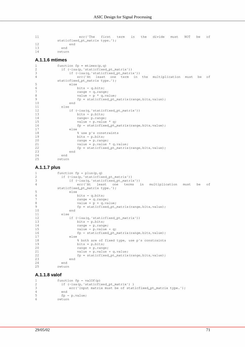
ASIC Design for Signal Processing
29/05/02 71
11 err('The first term in the d ivide must NOT be of staticfixed_pt_matrix type.');
12 end 13 end 14 return
A.1.1.6 mtimes 1 function fp = mtimes(p,q) 2 if (~isa(p,'staticfixed_pt_matrix')) 3 if (~isa(q,'staticfixed_pt_matrix')) 4 err('At least one term in the multiplication must be of
staticfixed_pt_matrix type.'); 5 else 6 bits = q.bits; 7 range = q.range; 8 value = p * q.value; 9 fp = staticfixed_pt_matrix(range,bits,value); 10 end 11 else 12 if (~isa(q,'staticfixed_pt_matrix')) 13 bits = p.bits; 14 range= p.range; 15 value = p.value * q; 16 fp = staticfixed_pt_matrix(range,bits,value); 17 else 18 % use p's constraints 19 bits = p.bits; 20 range = p.range; 21 value = p.value * q.value; 22 fp = staticfixed_pt_matrix(range,bits,value); 23 end 24 end 25 return
A.1.1.7 plus 1 function fp = plus(p,q) 2 if (~isa(p,'staticfixed_pt_matrix')) 3 if (~isa(q,'staticfixed_pt_matrix')) 4 err('At least one terms in multiplication must be of
st aticfixed_pt_matrix type.'); 5 else 6 bits = q.bits; 7 range = q.range; 8 value = p + q.value; 9 fp = staticfixed_pt_matrix(range,bits,value); 10 end 11 else 12 if (~isa(q,'staticfixed_pt_matrix')) 13 bits = p.bits; 14 range = p.range; 15 value = p.value + q; 16 fp = staticfixed_pt_matrix(range,bits,value); 17 else 18 % both are of fixed type, use p's constraints 19 bits = p.bits; 20 range = p.range; 21 value = p.value + q.value; 22 fp = staticfixed_pt_matrix(range,bits,value); 23 end 24 end 25 return
A.1.1.8 valof 1 function fp = valOf(p) 2 if (~isa(p,'staticfixed_pt_matrix') ) 3 err('Input matrix must be of staticfixed_pt_matrix type.'); 4 end 5 fp = p.value; 6 return

ASIC Design for Signal Processing
29/05/02 72
A.1.2 Output of test data to a file
This function writes the contents of a matrix to a file, in text format. It works by generating the
integer value of the binary number that represents the data. For example, the number 5.25,
encoded as 010101 would be written to the file as 21.
1 function output_matrix(fid, matrix, a_bits, a_frac, desc) 2 3 if ndims(matrix) ~= 2 4 err('Input matrix must be two dimensional for file output!'); 5 end 6 fprintf(fid,' ---------------------- '); 7 fprintf(fid,desc); 8 fprintf(fid,' \ r \ n'); 9 siz = size(matrix); 10 a_height = siz(1); 11 a_width = siz(2); 12 a = ones(a_height, a_width); 13 for rows = 1:a_height, 14 fprintf(fid,' '); 15 for columns=1:a_width, 16 %-- a(rows,columns) = matrix(rows,columns)*2^(a_bits - a_frac) -
2^(a_bits - a_frac - 1); 17 fprintf(fid,'%8.0f ',floor(matrix(rows,columns)*2^a_frac)); 18 end 19 fprintf(fid,' \ r \ n'); 20 end 21 fprintf(fid,' \ r \ n'); 22 23 for rows = 1:a_height, 24 fprintf(fid,' '); 25 for columns=1:a_width, 26 % a(rows,columns) = a(rows,columns) + j*(rand*2^(a_bits - a_frac)
- 2^(a_bits - a_frac - 1)); 27 fprintf(fid,'%8.0f
',floor(imag(matrix(rows,columns )*2^a_frac))); 28 end 29 fprintf(fid,' \ r \ n'); 30 end 31 fprintf(fid,' \ r \ n'); 32 33 return 34

ASIC Design for Signal Processing
29/05/02 73
$SSHQGL� %� )ORZFKDUW � R�
6LJQD � 3URFHVVR � ([HFXWLRQ
The signal processor architecture is made up of four pipeline stages:
• read data from memory
• delay to allow data to arrive from memory
• Multipli cation of data
• Output of results and/or tall ying data for later use
Each of the four stages consists of the following basic design:
The behaviour of the specific signals are described in chapter 6. The following sections of this
appendix detail the flowcharts for each of the pipeline stages.
NOTE: Although flowcharts are sequential by nature, a feature of VHDL is that signal
assignments within a process statement do not occur until either
• The end of the process statement is reached
• A time delay or wait statement is reached
Hence, assignments of the form a<= b in these flow charts should be read as “b is the value that
will be assigned to a, but the assignment will not take place until the termination point of this
flow chart” .
Begin
End
rst = '1'
rising clockedge
restart= '0''
running
stage_running
do mode/stage specific operationsnext_stage_running <= true;
next_stage_running <= false;
reset to state o f firstcycle o f firstoperation
true
truefalse
false
truefalse
true
yes
false
no
reset certainsignals

ASIC Design for Signal Processing
29/05/02 74
B.1. Read Stage
B.1.1 Mode 0 – Multiplication o f B * B*
Begin
mode0_delayedmode0_delayed <= false;do_wrt <= '0'; T rue
mode0_do two=mode0_counter
False
do_wrt <= '0';mode0_counter <= '1';mode0_read_address <= mode0_address2;
mode0_address1=xx11111
do_wrt='1';
mode0_address2=1111111
FalseTrue
True
mode0_address1 <= mode0_base1 + "0100000";mode0_address2 <= mode0_base1 + "0100000";mode0_read_address <= mode0_base1 + "0100000";mode0_base1 <= mode0_base1 + "0100000";diagonal <= true;
mode0_address1=1111111
True
mode <= "001";rtog_delayed <= q_toggle xo r '1';delay_running <= true;mode0_delayed <=false;outbase <= "0000";int_out_addr <= "0000";read_delay <= '1';
outbase <= outbase + "0101";int_out_addr <= outbase + "0101";mode0_delayed <= true;delay_running <= false;
True
False
mode0_address1 <= mode0_base1;mode0_address2 <= mode0_address2 + "0000001";mode0_read_address <= mode0_base1;diagonal <= false;int_out_addr <= int_out_addr + "0001";
do_wrt <= '0';mode0_address1 <= mode0_address1 + "0000001";mode0_address2 <= mode0_address2 + "0000001";mode0_read_address <= mode0_address1 + "0000001";
False
False
End
mode0_counter <= '0';
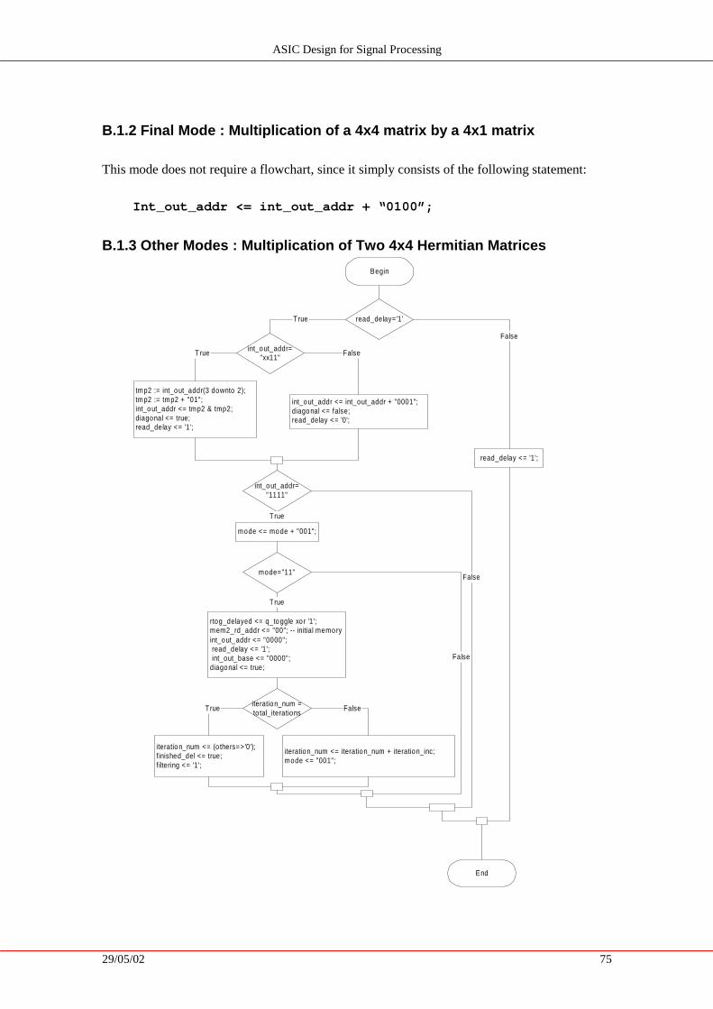
ASIC Design for Signal Processing
29/05/02 75
B.1.2 Final Mode : Multiplication of a 4x4 matrix by a 4x1 matrix
This mode does not require a flowchart, since it simply consists of the following statement:
Int_out_addr <= int_out_addr + “0100”;
B.1.3 Other Modes : Multiplication of Two 4x4 Hermitian Matrices
Begin
read_delay='1'
End
int_out_addr="xx11"
tmp2 := int_out_addr(3 downto 2);tmp2 := tmp2 + "01";int_out_addr <= tmp2 & tmp2;diagonal <= true;read_delay <= '1';
int_out_addr <= int_out_addr + "0001";diagonal <= false;read_delay <= '0';
T rue False
True
int_out_addr="1111"
mode <= mode + "001";
mode="11"
rtog_delayed <= q_toggle xo r '1';mem2_rd_addr <= "00"; -- initial memoryint_out_addr <= "0000"; read_delay <= '1'; int_out_base <= "0000";diagonal <= true;
iteration_num =to tal_iterations
iteration_num <= (o thers=>'0');f inished_del <= true;f iltering <= '1';
iteration_num <= iteration_num + iteration_inc;mode <= "001";
True False
True
True
False
False
read_delay <= '1';
False

ASIC Design for Signal Processing
29/05/02 76
B.2. Multiplication Stage
B.2.1 Mode 0 : Multiplication of B * B*
Begin M ultiplierM o de 0
End M ultiplierM o de 0
Set multiplierenable pins(see 6.7.1)
mul_diagonal
enable multiplicatio ninput data1 := data from memoryinput data2 := data from memory
enable multiplicatio ninput data1 := sto red datainput data2 := data from memory
mo de0_second_stage
disable multiplicationsto red data <= data fro m memo ry
true false
true false

ASIC Design for Signal Processing
29/05/02 77
B.2.2 Other modes
Begin M ultiplierM o de
End M ultiplierM o de
Set multiplierenable pins(see 6.7.1)
mul_diagonal
input data2 := data from memorysto red_ro w <= input data2
input data2 := data from inputs
multiplier_mode=final mode
input data 2 := sto red_row
false true
false false
enable multiplicatio ninput data1 := data from memory

ASIC Design for Signal Processing
29/05/02 78
B.3. Output Stage
Begin Output S tage
End Output M ode
comb_second_out = '1'
out_real and out_imag := conjugate o f sto red values
comb_mode ="000"
Add results to tally
comb_wrt= '1'
set out_real, out_imagclear talliescomb_second_out <= comb_diagonal
sto re tallies
comb_second_out <= comb_diagonalperfo rm mode specific manipulationsset out_real and out_imag
sto re out_real and out_imagcreate second write address
out_real o rout_imag out o f
range
clamp out-o f-rangecomponents atmax/min value
W rite to theappropriate
memory

ASIC Design for Signal Processing
29/05/02 79
$SSHQGL � &� 7HVWL ��� 9+' � &RGH
C.1. Multiplier Testbench
C.1.1 VHDL Code
The multiplier test benches were based on a design that had already been built for the original
10x10 multiplier. However, it required extensive modification in order to work for my
generically sizable multipliers.
C.1.1.1 Exhaustive Testbench 1 --------------------------------------------------------------- ------------------
--- 2 -- exhaustive_testbench.vhd, Testbench for recursive booth multiplier (recmult). 3 -- Author : Geoff Knagge 4 -- Created : 11 DEC 2001 5 -- Modified : 13 DEC 2001 6 -- 7 -- This testbench exhaustively tests all combinations of input for the given word 8 -- sizes. The simulator needs to run for (20 * 2^data_width_a + s^data_width_b
+20) ns 9 ---------------------------------------------------------------------------------
--- 10 11 12 library IEEE; 13 14 use IEEE.std_logic_1164.all; 15 use IEEE.std_logic_arith.a ll; 16 use ieee.std_logic_signed.all; 17 use ieee.std_logic_unsigned.all; 18 use std.textio.all; 19 20 library work; 21 22 entity exhaustive_testbench is 23 generic(data_width_a : integer :=5; 24 data_width_b : integer :=10; 25 carry_save : std_logic :='1 '); 26 end exhaustive_testbench; 27 28 architecture behaviour of exhaustive_testbench is 29 30 constant outwidth : integer := data_width_a + data_width_b - 1; 31 32 33 component arrmult 34 generic (data_width_a : integer:=10; -- number of bits in input a 35 data_width_b : integer:=10; -- number of bits in input b 36 carry_save : STD_LOGIC:='1'); -- whether or not to use the
final adder 37 38 port (signal in0 : in signed(data_width_a - 1 downto 0); 39 signal in1 : in sign ed(data_width_b - 1 downto 0); 40 signal ena : in STD_LOGIC; 41 signal sum : out signed(data_width_a + data_width_b - 2 downto 0); 42 signal carry : out signed(data_width_a + data_width_b - 2 downto 0)); 43 44 end component; 45 46 signal clk : std_logic := '0'; 47
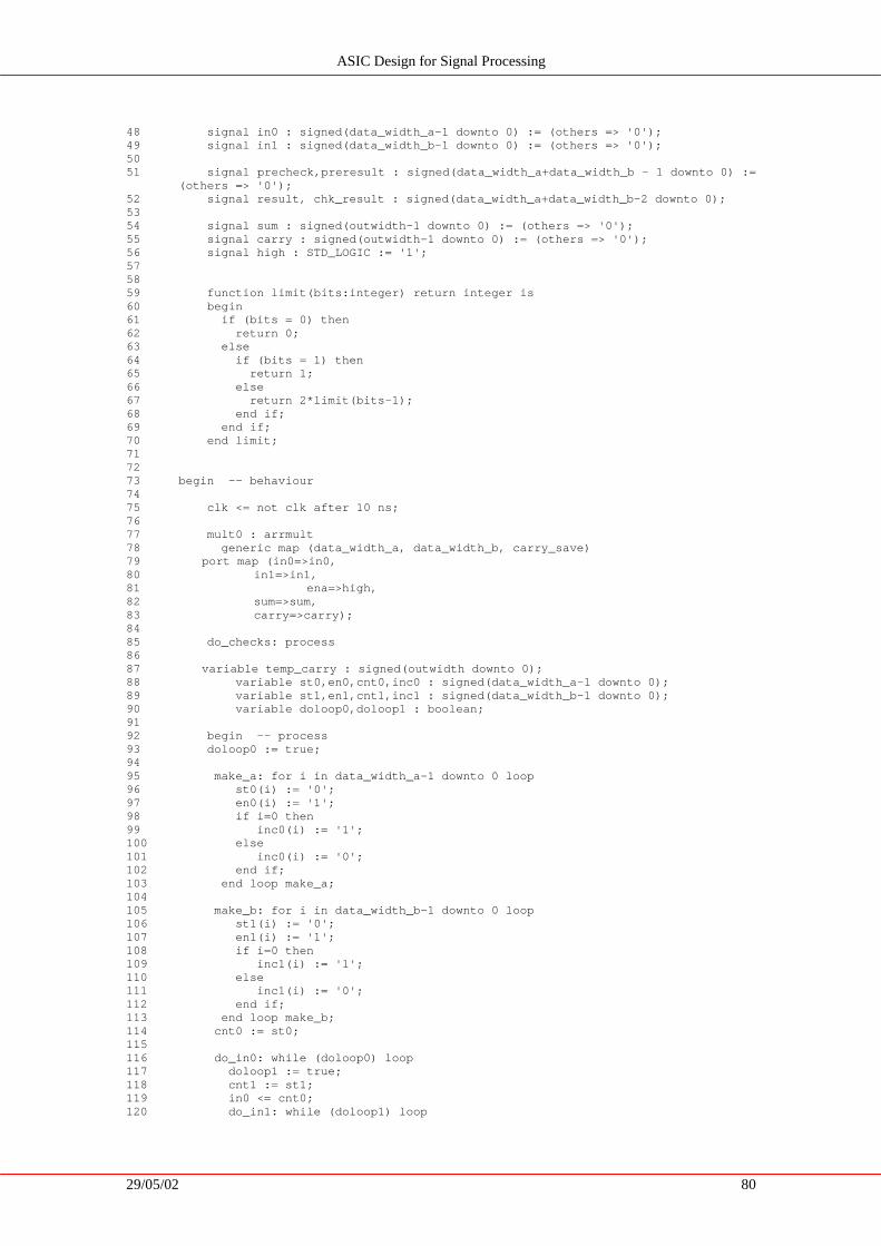
ASIC Design for Signal Processing
29/05/02 80
48 signal in0 : signed(data_width_a - 1 downto 0) := (others => '0'); 49 signal in1 : signed(data_width_b - 1 downto 0) := (others => '0'); 50 51 signal precheck,preresult : signed(data_width_a+data_width_b - 1 downto 0) :=
(other s => '0'); 52 signal result, chk_result : signed(data_width_a+data_width_b - 2 downto 0); 53 54 signal sum : signed(outwidth - 1 downto 0) := (others => '0'); 55 signal carry : signed(outwidth - 1 downto 0) := (others => '0'); 56 signal high : STD_LOGIC := '1' ; 57 58 59 function limit(bits:integer) return integer is 60 begin 61 if (bits = 0) then 62 return 0; 63 else 64 if (bits = 1) then 65 return 1; 66 else 67 return 2*limit(bits - 1); 68 end if; 69 end if; 70 end limi t; 71 72 73 begin -- behaviour 74 75 clk <= not clk after 10 ns; 76 77 mult0 : arrmult 78 generic map (data_width_a, data_width_b, carry_save) 79 port map (in0=>in0, 80 in1=>in1, 81 ena=>high, 82 sum=>sum, 83 carry=>carry); 84 85 do_check s: process 86 87 variable temp_carry : signed(outwidth downto 0); 88 variable st0,en0,cnt0,inc0 : signed(data_width_a - 1 downto 0); 89 variable st1,en1,cnt1,inc1 : signed(data_width_b - 1 downto 0); 90 variable doloop0,doloop1 : boolean; 91 92 begin -- process 93 doloop0 := true; 94 95 make_a: for i in data_width_a - 1 downto 0 loop 96 st0(i) := '0'; 97 en0(i) := '1'; 98 if i=0 then 99 inc0(i) := '1'; 100 else 101 inc0(i) := '0'; 102 end if; 103 end loop make_a ; 104 105 make_b: for i in data_width_b - 1 downto 0 loop 106 st1(i) := '0'; 107 en1(i) := '1'; 108 if i=0 then 109 inc1(i) := '1'; 110 else 111 inc1(i) := '0'; 112 end if; 113 end loop make_b; 114 cnt0 := st0; 115 116 do_in0 : while (doloop0) loop 117 doloop1 := true; 118 cnt1 := st1; 119 in0 <= cnt0; 120 do_in1: while (doloop1) loop

ASIC Design for Signal Processing
29/05/02 81
121 in1 <= cnt1; 122 wait until clk'event and clk='0'; 123 temp_carry(outwidth - 1 downto 1) := carry(outwidth - 2 downto 0); 124 t emp_carry(outwidth) := '0'; 125 temp_carry(0) := '0'; 126 127 128 preresult <= sum + temp_carry; 129 result(outwidth - 1 downto 0) <= preresult(outwidth - 1 downto 0); -- strip
off the unwanted extra bit... 130 131 precheck <= cnt0*cnt1; 132 chk_r esult(outwidth - 1 downto 0) <= precheck(outwidth - 1 downto 0); 133 134 assert result = chk_result report "Calculation Failed" severity error; 135 wait until clk'event and clk='1'; 136 if cnt1=en1 then 137 doloop1 := false; 138 else 139 cnt1 := cnt1 + inc1; 140 end if; 141 142 end loop do_in1; 143 144 if cnt0 = en0 then 145 doloop0 := false; 146 else 147 cnt0 := cnt0 + inc0; 148 end if; 149 end loop do_in0; 150 151 end process do_checks; 152 153 end beha viour;
C.1.1.2 Random Testbench 1 -----------------------------------------------------------------------------
------- 2 -- random_testbench.vhd, Testbench for booth multiplier (arrmult). 3 -- Author : Geoff Knagge 4 -- Created : 11 DEC 2001 5 -- Modified : 22 JAN 200 2 6 -- 7 -- This testbench randomly picks values for testing the multiplier. There is
an 80% 8 -- chance on each input that it will pick one of the extreme values 9 -----------------------------------------------------------------------------
------- 10 11 12 library IEEE ; 13 14 use IEEE.std_logic_1164.all; 15 use IEEE.std_logic_arith.all; 16 use ieee.std_logic_signed.all; 17 use ieee.std_logic_unsigned.all; 18 use std.textio.all; 19 20 library work; 21 22 23 entity random_testbench is 24 generic(data_width_a : integer :=5; 25 data_width_b : integer :=10; 26 carry_save : std_logic :='1'; 27 seedin : integer :=7); 28 end random_testbench; 29 30 architecture behaviour of random_testbench is 31

ASIC Design for Signal Processing
29/05/02 82
32 constant outwidth : integer := data_width_a + data_width_b - 1; 33 34 35 component arrmult 36 generic (data_width_a : integer:=10; -- number of bits in input a 37 data_width_b : integer:=10; -- number of bits in input b 38 carry_save : STD_LOGIC:='1'); -- whether or not to use the
final adder 39 40 port (sig nal in0 : in signed(data_width_a - 1 downto 0); 41 signal in1 : in signed(data_width_b - 1 downto 0); 42 signal ena : in STD_LOGIC; 43 signal sum : out signed(data_width_a + data_width_b - 2 downto 0); 44 signal carry : out signed(data_width_a + data_width_b - 2 downto
0)); 45 46 end component; 47 48 signal clk : std_logic := '0'; 49 50 signal in0 : signed(data_width_a - 1 downto 0) := (others => '0'); 51 signal in1 : signed(data_width_b - 1 downto 0) := (others => '0'); 52 53 signal precheck,preresult : signed(data_width_a+data_width_b - 1 downto
0) := (others => '0'); 54 signal result, chk_result : signed(data_width_a+data_width_b - 2 downto 0); 55 56 signal sum : signed(outwidth - 1 downto 0) := (others => '0'); 57 signal high: STD_LOGIC := '1'; 58 signal carry : signed(outwidth - 1 downto 0) := (others => '0'); 59 60 function limit(bits:integer) return integer is 61 begin 62 if (bits = 0) then 63 return 0; 64 else 65 if (bits = 1) then 66 return 1; 67 else 68 return 2*limit(bits - 1); 69 end if; 70 end if; 71 end limit; 72 73 -- random number generator taken from
http://home.europa.com/~celiac/archive/tidbit13.txt 74 procedure RANDOM (variable Seed: inout integer; variable X_real: out re al)
is 75 ---------------------------------------------------------------------- 76 -- Random Number generator from: 77 -- The Art of Computer Systems Performance Analysis, R.Jain 1991 (p443) 78 -- x(n) := 7^5x(n - 1) mod (2^31 - 1) 79 -- This has period 2^31 - 2, and it works with odd or even seeds 80 -- This code does not overflow for 32 bit integers. 81 ---------------------------------------------------------------------- 82 constant a_int : integer := 16807; -- multiplier 7**5 83 constant m_int : integer := 2147483647; -- modulus 2**31 - 1 84 constant q_int : integer := 127773; -- m DIV a 85 constant r_int : integer := 2836; -- m MOD a 86 constant m_real : real := real(M_int); 87 88 variable seed_div_q : i nteger; 89 variable seed_mod_q : integer; 90 variable new_seed : integer; 91 92 begin 93 seed_div_q := seed / q_int; -- truncating integer division 94 seed_mod_q := seed MOD q_int; -- modulus 95 new_seed := a_int * seed_mod_q - r _int * seed_div_q; 96 if (new_seed > 0) then 97 seed := new_seed; 98 else 99 seed := new_seed + m_int; 100 end if;

ASIC Design for Signal Processing
29/05/02 83
101 X_real := (real(seed) / m_real)*100.0; 102 end RANDOM; 103 104 begin -- behaviour 105 106 clk <= not clk after 10 ns; 107 108 mult0 : arrmult 109 generic map (data_width_a, data_width_b, '1') 110 port map (in0=>in0, 111 in1=>in1, 112 ena=>high, 113 sum=>sum, 114 carry=>carry); 115 116 checker: process 117 variable unf1,unf2,unf3,unf4,unf5,unf6: real; -- Uniform :=
Ini tUniform(7, - 100.0, 100.0); 118 variable seed: integer; 119 variable temp_carry : signed(outwidth downto 0); 120 variable st0,en0,cnt0 : signed(data_width_a - 1 downto 0); 121 variable st1,en1,cnt1 : signed(data_width_b - 1 downto 0); 122 123 begin -- process 124 make_a: for i in data_width_a - 1 downto 0 loop 125 if i = data_width_a - 1 then 126 st0(i) := '0'; 127 else 128 st0(i) := '1'; 129 end if; 130 en0(i) := '1'; 131 end loop make_a; 132 133 make_b: for i in data_width_b - 1 downto 0 loop 134 if i = data_width_b - 1 then 135 st1(i) := '0'; 136 else 137 st1(i) := '1'; 138 end if; 139 en1(i) := '1'; 140 end loop make_b; 141 cnt0 := st0; 142 seed := seedin; 143 144 do_checks: while (true) loop 145 RANDOM(seed,unf1); 146 RANDOM(seed,unf2); 147 RANDOM(seed,unf3); 148 RANDOM(seed,unf4); 149 RANDOM(seed,unf5); 150 RANDOM(seed,unf6); 151 if (unf1 > 80.0) then 152 if (unf2 > 50.0) then 153 cnt0 := st0; 154 else 155 cnt0 := en0; 156 end if; 157 else 158 make_in0: for i in data_width_a - 1 downto 0 loop 159 RANDOM(seed,unf3); 160 if (unf3 > 50.0) then 161 cnt0(i) := '0'; 162 else 163 cnt0(i) := '1'; 164 end if; 165 end loop make_in0; 166 end if; 167 168 if (unf4 > 80.0) then 169 if (unf5 > 50.0) then 170 cnt1 := st1; 171 else 172 cnt1 := en1; 173 end if;

ASIC Design for Signal Processing
29/05/02 84
174 else 175 make_in1: for i in data_width_b - 1 downto 0 loo p 176 RANDOM(seed,unf6); 177 if (unf6>50.0) then 178 cnt1(i) := '0'; 179 else 180 cnt1(i) := '1'; 181 end if; 182 end loop make_in1; 183 end if; 184 185 in0 <= cnt0; 186 in1 <= cnt1; 187 wait unti l clk'event and clk='0'; 188 temp_carry(outwidth - 1 downto 1) := carry(outwidth - 2 downto 0); 189 temp_carry(outwidth) := ‘0’; 190 temp_carry(0) := ‘0’; 191 pre_result <= sum + temp_carry; 192 result(outwidth - 1 downto 0) <= preresult(outwidth - 1 downto 0); 193 precheck <= cnt0 * cnt1; 194 chk_result(outwidth - 1 downto 0) <= precheck(outwidth - 1 downto 0); 195 196 assert result= chk_result report “Calculation Failed” severity failure; 197 wait until clk’event and clk=’1’; 198 end loop do_checks; 199 end process checker; 200 end behaviour;

ASIC Design for Signal Processing
29/05/02 85
C.1.2 TCL Scripts
These scripts are used to run the ModelSim simulation tool, to automatically run the test
benches over various multiplier configurations.
C.1.2.1 Exhaustive Testbench 1 # This scripts runs tests on multipliers f rom size 2x2 up to 64x64 2 # 3 # Switch off the arithmetic package warnings... 4 set IgnoreWarning 1 5 # Run the exhaustive testbench on 3x3, ... 9x9 bit multipliers 6 for {set x 3} {$x<10} {incr x} { 7 echo Attempting to load simulation for $x x $x bit multiplier.. . 8 vsim - Gdata_width_a=$x - Gdata_width_b=$x - Gcarry_save='1'
work.exhaustive_testbench 9 set dw 1 10 set wid 1 11 while {$wid<=$x} { 12 set wid [expr $wid+1] 13 set dw [expr $dw *2] 14 } 15 set IgnoreWarning 1 16 set time [expr 20*$dw*$dw] 17 add wave sim :/exhaustive_testbench/* 18 echo Exhaustively testing $x x $x bit multiplier for $time ns... 19 run $time ns 20 echo Completed testing of $x x $x bit multiplier. 21 }
C.1.2.2 Random Testbench 1 # Switch off the arithmetic package warnings... 2 set IgnoreWarning 1 3 # Run th e random testbench on 10x10, 11x11, ... 64x64 bit multipliers 4 for {set x 10} {$x<64} {incr x} { 5 echo Attempting to load simulation for $x x $x bit multiplier... 6 # 7 # randomly pick a random seed for the testbench, to improve its randomness 8 set seed [ expr {int(rand()*1001)+2}]; 9 # 10 # do one test, with no final adder on the carry - save outputs 11 vsim - Gdata_width_a=$x - Gdata_width_b=$x - Gcarry_save='1' - Gseedin=$seed
work.random_testbench 12 set IgnoreWarning 1 13 # 14 # display all signals so that we can examine them if something goes wrong 15 add wave sim:/random_testbench/* 16 echo Randomly testing $x x $x bit multiplier for 1ms... 17 run 1 ms 18 echo Completed testing of $x x $x bit multiplier. 19 }