asian power electronics journal - perc homeperc.polyu.edu.hk/apej/apej/volume4/no2/vol 4...
TRANSCRIPT

i
Asian Power Electronics Journal PERC, HK PolyU

ii
Copyright © The Hong Kong Polytechnic University 2010 All right reserved. No part of this publication may be reproduced or transmitted in any form or by any means, electronic or mechanical, including photocopying recording or any information storage or retrieval system, without permission in writing form the publisher. First edition August 2010 Printed in Hong Kong by Reprographic Unit The Hong Kong Polytechnic University Published by Power Electronics Research Centre The Hong Kong Polytechnic University Hung Hom, Kowloon, Hong Kong ISSN 1995-1051 Disclaimer Any opinions, findings, conclusions or recommendations expressed in this material/event do not reflect the views of The Hong Kong Polytechnic University

Asian Power Electronics Journal, Vol. 4 No.2 August 2010
iii
Editorial board Honorary Editor Prof. Fred C. Lee Electrical and Computer Engineering, Virginia Polytechnic Institute and State University Editor Prof. Yim-Shu Lee Victor Electronics Ltd. Associate Editors and Advisors Prof. Philip T. Krien Department of Electrical and Computer Engineering, University of Illinois Prof. Keyue Smedley Department of Electrcial and Computer Engineering, University of California Prof. Muhammad H. Rashid Department of Electrical and Computer Engineering, University of West Florida Prof. Dehong Xu College of Electrical Engineering, Zhejiang University Prof. Hirofumi Akagi Department of Electrical Engineering, Tokyo Institute of Technology Prof. Xiao-zhong Liao Department of Automatic Control, Beijing Institute of Technology Prof. Wu Jie Electric Power College, South China University of Technology Prof. Hao Chen Dept. of Automation, China University of Mining and Technology Prof. Danny Sutanto Integral Energy Power Quality and Reliability Centre, University of Wollongong Prof. Siu L.Ho Department of Electrical Engineering, The Hong Kong Polytechnic University Prof. Eric Cheng Department of Electrical Engineering, The Hong Kong Polytechnic University Dr. Norbert Cheung Department of Electrical Engineering, The Hong Kong Polytechnic University Dr. Kevin Chan Department of Electrical Engineering, The Hong Kong Polytechnic University Dr. Tze F. Chan Department of Electrical Engineering, The Hong Kong Polytechnic University Dr. Edward Lo Department of Electrical Engineering, The Hong Kong Polytechnic University Dr. Mark Ho Department of Electrical Engineering, The Hong Kong Polytechnic University Dr. David Cheng Department of Industrial and System Engineering, The Hong Kong Polytechnic University Dr. Martin Chow Department of Electronic and Information Engineering, The Hong Kong Polytechnic University Dr. Frank Leung Department of Electronic and Information Engineering, The Hong Kong Polytechnic University

Asian Power Electronics Journal, Vol. 4 No.2 August 2010
iv
Publishing Director: Prof. Eric Cheng Department of Electrical Engineering, The Hong Kong Polytechnic University Communications and Development Director: Ms. Anna Chang Department of Electrical Engineering, The Hong Kong Polytechnic University Editorial Committee: Prof. Bhim Singh Prof. B.P.Divakar Prof. Dehong Xu Prof. K.Keerthivasan Prof. Wang xiaoyuan Prof. Xiaozhong Liao Prof. Xie Yue Prof. Y. B. Che Prof. Zhe Chen Dr. Benny Y.P.Yeung Dr. B. Geethalakshmi Dr. B.Vinod Dr. C. Christober Asir Rajan Dr. Chi Kwan Lee Dr. Dong Ping Dr. Dong Lei Dr. Durairaj Dr. E. Chandra Sekaran Dr. Frank H. Leung Dr. Gao Yanxia Dr. James Ho Dr. Kai Ding Dr. Lu Yan Dr. Martin Chow Dr. Mohan V Aware Dr. Patrick C. K.Luk Dr. P.Ajay-D-Vimal Raj Dr. Prasad Dr. R. Zaimeddine Dr. S. Chandramohan Dr. Sudhir Kumar Srivastava Dr. Seyed Saeed Fazel Dr. Shu Jie Dr. S. P. Natarajan Dr. S. X.Wang Dr. Tze F. Chan Dr. Wai Chwen Gan Dr. W. N. Fu Dr. Xue Xiang Dang Dr. Yang Jinming Dr. Zeng Jun. Dr. Z. Y. Dong

Asian Power Electronics Journal, Vol. 4 No.2 August 2010
v
Production Coordinator: Mr. Ken Ho Power Electronics Research Centre, The Hong Kong Polytechnic University Secretary: Ms. Canary Tong Department of Electrical Engineering, The Hong Kong Polytechnic University

Asian Power Electronics Journal, Vol. 4 No.2 August 2010
vi
Table of Content Design and Development of an Optimal Capacitor Charger D. Louhibi, R. Beggar, F. Almabouada and A. Noukaz
46
Modeling and Simulation of Wind Turbine Driven Permanent Magnet Generator with New MPPT Algorithm R. Bharanikumar, A.C. Yazhini and A. Nirmal Kumar
52
Improvemed Power Quality Using Photovoltaic Unified Static Compensation Techniques Narayanappa and K.Thanushkodi
59
Frequency Domain Analysis of Adjustable Speed Drive Systems Based on Transfer Switching Function V. Mohan, J. Raja and S. Jeevananthan
64
On Closed-loop Decoupling Control Strategy for Grid-connected Double-fed Generator CHE Yanbo, WANG Yu and WANG Chengshan
69
Integrated Electronic Load Controller with T-Connected Transformer for Isolated Asynchronous Generator Bhim Singh and V. Rajagopal
74
Author Index 81
Asian Power Electronics Journal, Vol. 4 No.2 August 2010
46
Design and Development of an Optimal Capacitor Charger
D. Louhibi1 R. Beggar2 F. Almabouada3 A. Noukaz4
Abstract – With coupled inductances, we can load a capacitor placed in parallel with the secondary inductance by the transfer of magnetic energy stored in the primary inductance (flyback principle). Calculations have shown that the time required to the complete energy transfer decreases with the incremental initial value of the voltage between the terminals of the capacitor. That behaviour has led us to model a simple circuit (based on the NE555) which allows minimizing dead time between the command pulses of the switching transistor in order to optimize the speed of the charge. For this optimization only the sensing of the capacitor voltage is needed. The simulation of the model allowed us to confirm the theoretical estimations. The experimental results are in good agreement with those obtained by the simulation performed by MicroSim Relase 8 which constituted a validation of our model. Keywords – Flyback, capacitor charger, energy-storage capacitor, flash lamp pumping.
I. INTRODUCTION The capacitor discharge is a widely used technique in excitation systems, especially for those intended to excite pulsed lasers and plasma-based systems [1]. With the development of new efficient semiconductor components, such as IGBTs (Isolated Gate Bipolar Transistor), capacitor charger systems become solely based on the principle of SMPS (Switch Mode Power Supply). Many previous works have been achieved in this context with various topologies. The latter mainly consist of forward configuration, Full bridge configuration [2-3], H-bridge configuration [4-5] and flyback configuration [6]. We have also opted for a flyback configuration, where the primary and the secondary excitation current are uncoupled. Indeed the capacitor charge results from energy transfer. Unlike Sokal [6], we have chosen a system with a complete energy transfer. The minimization of the time between the command pulses of the switching transistor is based on a relationship predetermined analytically and carried out with a simple an intelligent circuit based on a NE555. For this control, only the sensing of the capacitor voltage is needed. That avoids difficulties and perturbations inherent to secondary current measurement. The discrete pulse number allowing the load of the capacitor is determined according to the energy value transferred per pulse, the loading duration and the total energy to load. Our system stops the charge when this one reaches a predetermined value. Also our charging system doesn’t need an auxiliary wending to detect the demagnetization of the transformer core and the driving circuit doesn’t need a soft-start feature as a conventional driving circuit. The paper first received 7 July 2009 and in revised form 22 Mar 2010. Digital Ref: Digital Ref: A170701234 Centre de Développement des Technologies Avancées, Algérie, 1E-mail: [email protected]; 2 E-mail: [email protected]; 3 E-mail: [email protected] ; 4 E-mail: [email protected]
II. FUNDAMENTAL RELATIONS
The basic flyback circuit is given in Fig 1. [7]
Fig. 1: Flyback circuit
The primary current pulse ip, the secondary current pulse isk, the switching command pulses V and the voltage of the capacitor C are respectively represented in Fig 2. The variation of the primary current flowing through the primary winding of the transformer writes:
τtI)t(i maxPP =
(1)
where IPmax is the maximum primary current, t is the time and τ is the pulse command width of the switching transistor (S) as shown in figure 2. The maximal primary current is:
τP
p LEI =max
(2)
where E is the rectified and filtered main power voltage and LP is the primary inductance. The secondary current varies according to the relationship:
( ) ( )tsinZ
VtcosI)t(i 0
C0maxSS
1kk
ωω −−= (3)
with:
CLS
10 =ω ,
CL
Z S=
where ISmax is the maximum secondary current, LS is the secondary inductance, C is the storage capacitor, Vck-1 is the storage capacitor voltage and the index k is an integer and corresponds to the kth pulse. The transfer of the stored energy in the magnetic circuit towards the capacitor C is complete when the secondary current is cancelled. We can thus deduce the needed time for the energy transfer from a pulse to another as follows:
⎟⎟
⎠
⎞
⎜⎜
⎝
⎛ ⋅=
−1kC
maxS
0k V
IZarctg1t
ωΔ
(4)

D. Louhibi et.al: Design and Development…..
47
We notice that ktΔ decreases as 1−kCV increases.
For: 1kCmaxS V)IZ(−
<<⋅ , equation (4) becomes:
⎟⎟
⎠
⎞⎜⎜
⎝
⎛ ⋅=
−1kC
maxS
0k V
IZ1tω
Δ (5)
The evolution of kCV from pulse to pulse is given as:
⎥⎥⎦
⎤
⎢⎢⎣
⎡
⎟⎟
⎠
⎞
⎜⎜
⎝
⎛ ⋅
⋅=
−1k
k
C
maxs
maxSC
VIZarctgsin
IZV (6)
Fig. 2: Temporal variation of the primary current pulses,
the secondary current pulses and the voltage of C.
As shown in Fig 2 the necessary time to the cancellation of the secondary current decreases from a pulse to another. To allow the complete demagnetization of the transformer’s secondary winding for the first pulse we must choose a period great or equal to )t( 1 τΔ + . But if we use this fixed period the lost time would increase between the next pulses and the load of C would be slowed down. To solve this problem we had to minimize this dead time, in other way to compress these command pulses.
III. MODELLING
Fig. 3: The Synoptic scheme of the system.
The purpose is to design an electronic circuit which supplies pulses to the switch depending on the voltage load capacitor. The low level width of these pulses has to vary in the same manner as the time necessary to cancellation of the secondary winding current. The scheme of this system appears in Fig 3. The circuit which allows following the variation of ktΔ in
terms of 1−kCV is given in Fig 4.
Fig. 4: The scheme of the pulses compression circuit.
The designed circuit is based on a NE555 assembled in astable. The values of the components R, R1 and C1 (Fig 4) were calculated so that the period of the control signal (low level for Vc0=0V) performs a complete demagnetization of the secondary winding during the first energy transfer. The capacitor C1 discharges through R1 resistance during a fixed time representing the low level of the pulses at the output of the NE555, while the time of load of C1, which represents the high level, is modulated by sensing the storage capacitor voltage of C. The signal obtained at the output of the NE555 attacks the entry of the monostable of precision that provided the control signal to the switch having constant high level to fix the IPmax value and variable low level which follows the time of cancellation of the secondary current. This circuit also makes it possible to stop the load of C when this one reaches a predetermined value by blocking the monostable. As we see it on Fig. 4, the output voltage Vck-1 controls the base current of the transistor (T) through the feedback resistor RB. The emitter current charges the capacitor C1 of NE555. This transistor constitutes a current generator and can be schematized as in Fig 5. The calculation of the necessary time to charge the capacitor C1 of NE555 between 1/3 and 2/3 of supply voltage of the circuit Vcc gives the following relationship:
⎟⎟⎟⎟⎟
⎠
⎞
⎜⎜⎜⎜⎜
⎝
⎛
−
⋅
⋅⋅⋅+
+⋅⋅=− CC
D
BCC
C1k V
V6
RVVR3
1
11LnCRT1k
βΔ
(7)
where VD is the threshold voltage of the diodes D1 and D2 and β is the gain of the transistor (T),

Asian Power Electronics Journal, Vol. 4 No.2 August 2010
48
Fig. 5: The equivalent scheme of the current generator.
In the case where:
β.R.3RV.6Vc B
D1k >>− , the first term of the series
expansion of relation (7) gives the new relation:
VccV.6
R.VccVc..R.31
C.RTD
B
1k1
k−+
=−β
Δ (8)
In order to determine the value of the resistor R of the NE555 circuit, we rewrite the equations (4) and (7) for k=1 (Vck-1 =Vc0 =0V). The new equations are:
01 2
tωπΔ =
(9)
⎥⎥⎥⎥
⎦
⎤
⎢⎢⎢⎢
⎣
⎡
⎟⎠
⎞⎜⎝
⎛ −+=
VccV
.61
11Ln.C.RTD
11Δ
(10)
Equalising equations (9) and (10) we have:
Fig. 6: The variation of k
BR⎟⎟⎠
⎞⎜⎜⎝
⎛β
versus 1−kCV
⎥⎦
⎤⎢⎣
⎡−
=
CC
D10 V
V.62Ln.C..2R
ω
π (11)
For a fixed value of C1 we calculate the R value. Also from equalising equations (5) and (8) results the following expression:
)I.Z.V.6VccI.ZV.Vcc.C.R.(
V.R.3.I.Z)
R(
maxsDmaxsC10
Cmaxsk
B
1k
1k
+−=
−
−
ωβ
(12)
Fig 6 represents the variation of k
BR⎟⎟⎠
⎞⎜⎜⎝
⎛β
in terms of1kCV
−.
We notice on figure 6 that after a certain load voltage the
ratio k
BR⎟⎟⎠
⎞⎜⎜⎝
⎛β
tends to be constant. By choosing a
transistor with a known gain β we calculate the correspondent value of RB. The curve of both ktΔ and kTΔ (using equations (4), (6)
and (7)) versus 1−kCV for 5
k
B 10R=⎟⎟
⎠
⎞⎜⎜⎝
⎛β
kΩ, is
represented in figure 7.
Fig. 7: Variation of ktΔ and kTΔ versus1−kCV .
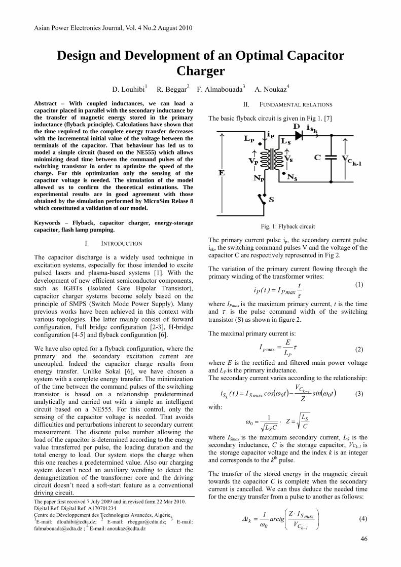
We notice on this figure that the two curves coincide that prove the efficiency of our model. We can see clearly from the Fig 8 that the pulses compression makes the capacitor charging faster. The curves represented in Figs 6, 7 and 8 were plotted by using the software Matlab.
D. Louhibi et.al: Design and Development…..
49
Fig. 8: Capacitor charging with and without pulses compression.
IV. SIMULATION
The proposed circuit was simulated with MicroSim Relase 8 software. The obtained results are given in the following figures.
Fig. 9: The primary and secondary currents without pulses
compression.
Fig. 10: The primary and secondary currents with pulses
compression.
Figs 9 and 10 show the variation of the primary and secondary currents without and with pulses compression.
These figures point out clearly the advantage of our circuit, which consists of practically complete delete of the dead time. We can also see this advantage in the charging process in Fig 11 where the charge is becoming faster.
Fig. 11: The capacitor charging with and without pulses
compression. The curves of the Figs 6, 7, 8, 9, 10 and 11 were obtained with the following parameters value: LS =14.3 mH, IPmax=10A, ISmax=2A, C=40µF, C1=82nF, VD =0.6V VCC=12V,
kBR
⎟⎠⎞⎜
⎝⎛
β=105 kΩ.
V. EXPERIMENTAL RESULTS
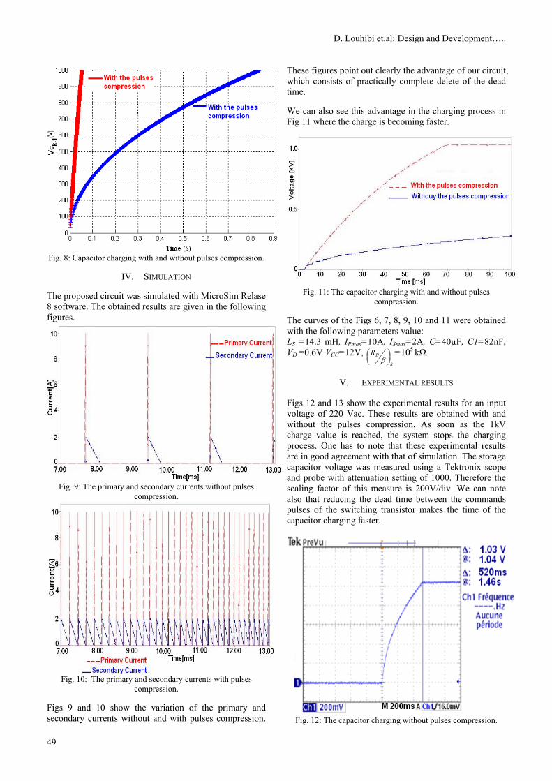
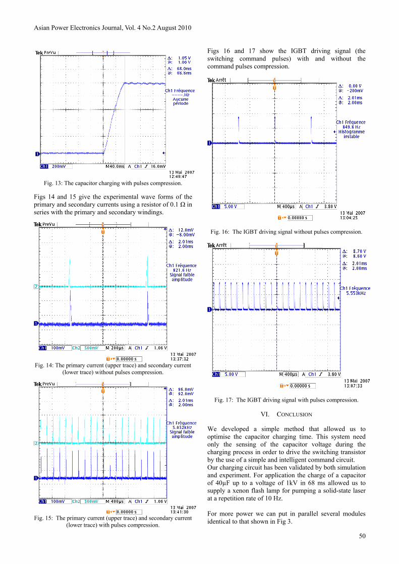
Figs 12 and 13 show the experimental results for an input voltage of 220 Vac. These results are obtained with and without the pulses compression. As soon as the 1kV charge value is reached, the system stops the charging process. One has to note that these experimental results are in good agreement with that of simulation. The storage capacitor voltage was measured using a Tektronix scope and probe with attenuation setting of 1000. Therefore the scaling factor of this measure is 200V/div. We can note also that reducing the dead time between the commands pulses of the switching transistor makes the time of the capacitor charging faster.
Fig. 12: The capacitor charging without pulses compression.
Asian Power Electronics Journal, Vol. 4 No.2 August 2010
50
Fig. 13: The capacitor charging with pulses compression.
Figs 14 and 15 give the experimental wave forms of the primary and secondary currents using a resistor of 0.1 Ω in series with the primary and secondary windings.
Fig. 14: The primary current (upper trace) and secondary current
(lower trace) without pulses compression.
Fig. 15: The primary current (upper trace) and secondary current
(lower trace) with pulses compression.
Figs 16 and 17 show the IGBT driving signal (the switching command pulses) with and without the command pulses compression.
Fig. 16: The IGBT driving signal without pulses compression.
Fig. 17: The IGBT driving signal with pulses compression.
VI. CONCLUSION
We developed a simple method that allowed us to optimise the capacitor charging time. This system need only the sensing of the capacitor voltage during the charging process in order to drive the switching transistor by the use of a simple and intelligent command circuit. Our charging circuit has been validated by both simulation and experiment. For application the charge of a capacitor of 40µF up to a voltage of 1kV in 68 ms allowed us to supply a xenon flash lamp for pumping a solid-state laser at a repetition rate of 10 Hz. For more power we can put in parallel several modules identical to that shown in Fig 3.
D. Louhibi et.al: Design and Development…..
51
REFERENCES
[1] W. Koechner, “Solid-State Laser Engineering” (Springer 6th ed, 2006).
[2] M. Gliesselmann and T. Heeren, “Rapid capacitor charger”, the twenty-fifth International IEEE Power Modulator Symposium, 2002 and 2002 High-Voltage Workshop. Vol, 30, June-3 July 2002, pp. 146-149.
[3] M. Gliesselmann, B. McHale and T. Heeren, “New developments in high power capacitor charging technology”, the twenty-sixth IEEE International Power Modulator Symposium, 2004 High-Voltage Workshop. 23-26 May 2004, pp.395-398.
[4] M. Gliesselmann, and E. Kristiansen “Design of 30kV power supply for rapid capacitor charging”, the twenty-fourth International IEEE Power Modulator Symposium, 26-29 June 2000, pp. 115-118.
[5] M. Gliesselmann, T. Heeren, T. Helle: “Compact High power capacitor charger”, the 14th International IEEE Pulsed Power Conference, Vol 1, 15-18 June 2003, pp.701-710.
[6] Nathan.O. Sokal and R. Redl, “Control Algorithms and Circuit Designs for Optimal Flyback-Charging of an Energy-Storage Capacitor (e.g., for Flash Lamp od Defibrillator) ”, IEEE Transactions on Power Electronics, Vol. 12, No 5, September 1997, pp. 885-894.
[7] M. Brown: “Practical Switching Power Supply Design”. Series in Solid State Electronics, Motorola, 1991, pp. 29-34.
BIOGRAPHIES
D. Louhibi obtained his engineer degree in electronic from the National Polytechnic College of Algiers in 1977 and his magister degree in quantum electronics in 1982 from the University of Science and Technology Houari Boumediene USTHB. He is a full-time reasercher at the CDTA (The Advanced Technologies development Center) since 1985 and in 2000 he was promoted as a master of research. he is also an associated teacher at the
USTHB. R. Beggar obtained his engineer degree in electronic from the University of Blida. He joined the CDTA (The Advanced Technologies development Center) in 2002 as an assistant reasercher. F. Almabouada obtained his engineer degree in electronic from the University of Blida. He joined the CDTA (The Advanced Technologies development Center) in 2004 as an assistant reasercher. A. Noukaz He is working in the CDTA since 1992 as a specialized engineer on laser electronic systems.
Asian Power Electronics Journal, Vol. 4 No.2 August 2010
52
Modeling and Simulation of Wind Turbine Driven Permanent Magnet Generator with New MPPT
Algorithm
R. Bharanikumar1 A.C. Yazhini2 A. Nirmal Kumar3
Abstract – This paper presents Maximum Power Point Control for variable speed wind turbine driven permanent-magnet generator. The wind turbine generator is operated such that the rotor speed varies according to wind speed to adjust the duty cycle of power converter and maximizes Wind Energy Conversion System (WECS) efficiency. The maximum power point for each speed value is traced using Maximum Power Point Tracking (MPPT) algorithm. The rotating speed of permanent-magnet generator should be adjusted in the real time to capture maximum wind power. The system includes the wind-turbine, permanent-magnet generator (PMG), three-phase rectifier, boost chopper, inverter and load. The control parameter is the duty cycle of the chopper. PMG is made to operate at variable speed to achieve good performance. The entire WECS model consists of wind turbine model, PMG model and power converters model. The MATLAB / SIMULINK are used for simulation and the results are compared with laboratory setup. Keywords – PMG, rectifier, boost chopper, inverter, wind turbine, MPPT.
I. NOMENCLATURE ρ - Air density A - Area swept by the blades Iq,Id - q - axis, d -axis current, respectively Xq,Xd - Reactance of q -axis , d - axis, respectively δ - Power Angle p - Differential Operator (d/dt) Te - Electromagnetic Torque produced V - Velocity of the Wind λ - Tip Speed Ratio ωt - Turbine Speed Tg - Generator Torque Vabc - Phase Voltages Rabc - Phase Resistances λabc - Flux Linkages in the phases β - Pitch Angle G - Gear ratio Cp - Power Coefficient
II. INTRODUCTION Consumption of energy based on fossil fuels is considered to be the major factor for global warming and environment degradation. The utilization of naturally occurring renewable energy sources as an alternative energy supply has been assuming more importance of less Power generation utilizing solar rays, geothermal energy, wind force and wave force has became a reality. The paper first received 8 July 2009 and in revised form 21 April 2010. Digital Ref: Digital Ref: A170701235 1, 2, 3 Department of Electrical and Electronics Engineering, Bannari Amman Institute of Technology, Anna University, TamilNadu India E-mail: [email protected]
Research on performance improvement of and cost reduction in such non–conventional energy conversion systems is being accorded the highest priority [8].Wind power generation has a strong connection to rotating machinery and hence its practical application is most promising. Wind generator control methods have already been proposed to efficiently utilize the wind power which is prone to fluctuation every moment. The induction type machine has the advantages of robustness, low cost and maintenance-free operation. However, they have the drawbacks of low power factor and need for an AC excitation source. Permanent magnet generator is chosen so as to eliminate the drawbacks of induction generator. Boost chopper circuit with a single switching device is the choice for power control that provides an improved efficiency [9]. For analysis of the above wind generator system, the generator and boost chopper are represented by their equivalent circuits. Performance characteristics such as generated output power and DC output voltage are expressed as functions of the duty cycle of chopper and shaft speed of generator. The power generated varies with load with the peak occurring at certain load. Therefore, the optimum duty cycle for maximum power can be deduced by differentiating the output power with respect to duty cycle. The validity of the technique for arriving at the maximum power is confirmed in the simulation study. In the present analysis, the value of each part is calculated on the basis of the rotational speed observed by the rotation sensor. Considerations of the characteristics of the wind mill are not necessary, because the torque is a function of the generator speed and characteristics of the wind mill are reflected in the rotational speed [8].
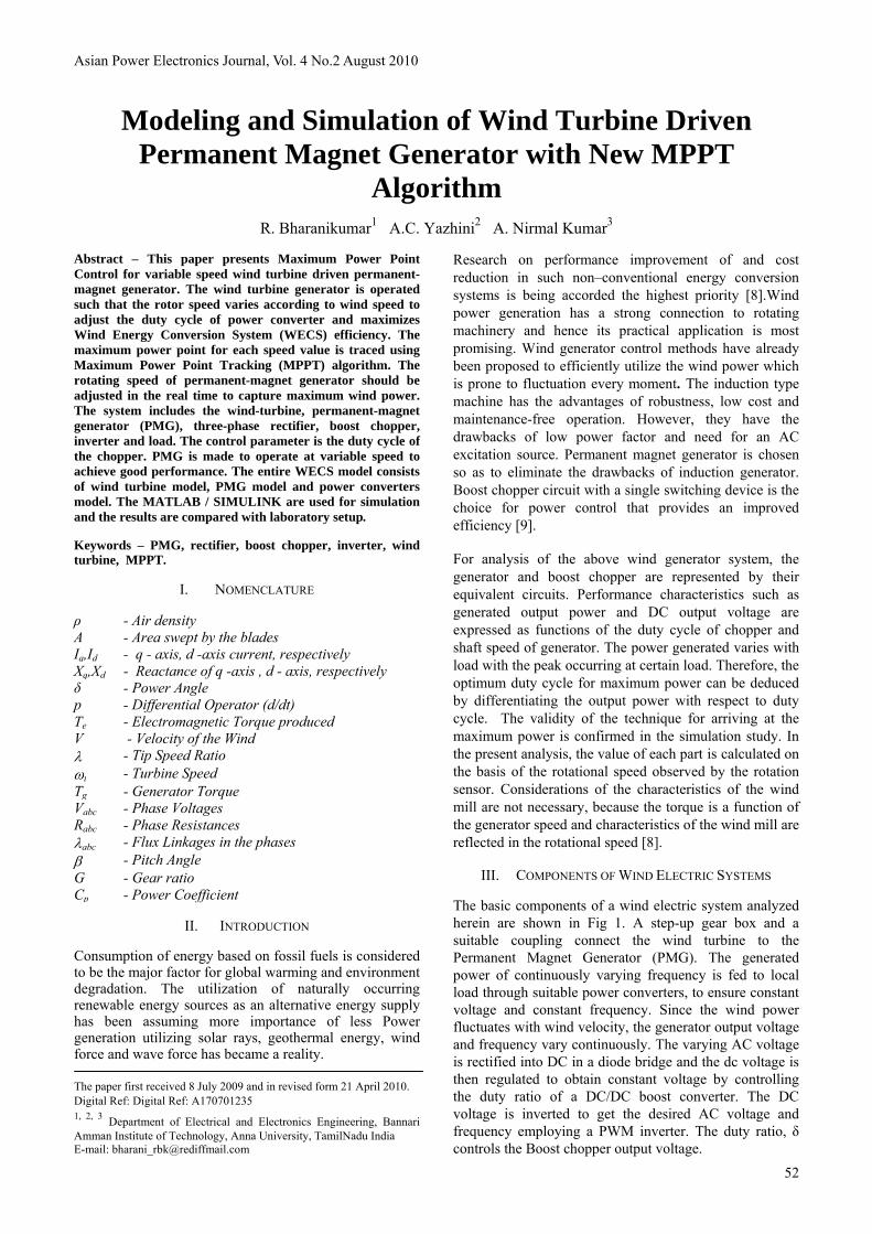
III. COMPONENTS OF WIND ELECTRIC SYSTEMS The basic components of a wind electric system analyzed herein are shown in Fig 1. A step-up gear box and a suitable coupling connect the wind turbine to the Permanent Magnet Generator (PMG). The generated power of continuously varying frequency is fed to local load through suitable power converters, to ensure constant voltage and constant frequency. Since the wind power fluctuates with wind velocity, the generator output voltage and frequency vary continuously. The varying AC voltage is rectified into DC in a diode bridge and the dc voltage is then regulated to obtain constant voltage by controlling the duty ratio of a DC/DC boost converter. The DC voltage is inverted to get the desired AC voltage and frequency employing a PWM inverter. The duty ratio, δ controls the Boost chopper output voltage.
R. Bharanikumar et.al: Modeling and Simulation…..
53
Fig. 1: Block diagram of wind electric generator system
IV. THEORETICAL ANALYSIS
A. Wind turbine model There are two types of wind turbines namely vertical axis and horizontal axis types. Horizontal axis wind turbines are preferred due to the advantages of ease in design and lesser cost particularly for higher power ratings. The power captured by the wind turbine is obtained as
3 212 pP R V Cπρ=
(1)
where the power coefficient Cp is a nonlinear function of wind velocity and blade pitch angle and is highly dependent on the constructive features and characteristics of the turbine. It is represented as a function of the tip speed ratio λ given by [2].
tRVω
λ = (2)
It is important to note that the aerodynamic efficiency is maximum at the optimum tip speed ratio. The torque value obtained by dividing the turbine power by turbine speed is formed obtained as follows:
( ) ( )2 31,2t t tT V R C Vω πρ λ=
(3)
where Ct (λ) is the torque co-efficient of the turbine, given by
( )( )p
tC
Cλ
λλ
= (4)
The power co-efficient is given by [3]
( ) ( )16.5
1116 0.4* 5 0.51pC e λλ βλ
−⎛ ⎞= − −⎜ ⎟⎝ ⎠
(5)
where
( )
1
3
1
1 0 .0 3 50 .0 8 9 1
λ
λ β β
=⎛ ⎞
−⎜ ⎟⎜ ⎟+ +⎝ ⎠
(6)
B. Permanent Magnet Generator Model Permanent Magnet Generator provides an optimal solution for varying-speed wind turbines, of gearless or single-stage gear configuration. This eliminates the need for separate base frames, gearboxes, couplings, shaft lines, and pre-assembly of the nacelle. The output of the generator can be fed to the power grid directly. A high level of overall efficiency can be achieved, while keeping the mechanical structure of the turbine simple.
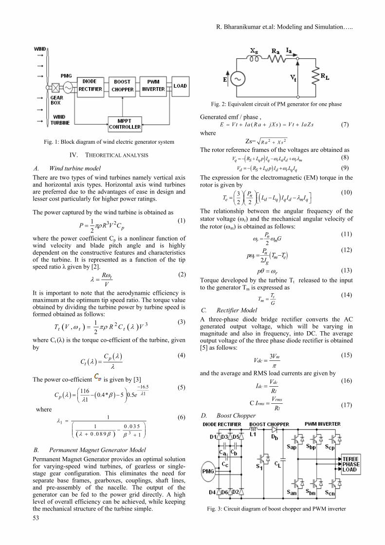
Fig. 2: Equivalent circuit of PM generator for one phase
Generated emf / phase ,
( )E V t Ia R a jX s V t Ia Z s= + + = + (7)where
Zs= 2 2R a X s+ The rotor reference frames of the voltages are obtained as
( )q S q q r d d r mV R L p I L Iω ω λ=− + − + (8)
( )d S d d r q qV R L p I L Iω=− + + (9)The expression for the electromagnetic (EM) torque in the rotor is given by
( )32 2
ne d q q d m q
PT L L I I Iλ⎛ ⎞⎛ ⎞ ⎡ ⎤= − −⎜ ⎟⎜ ⎟ ⎣ ⎦⎝ ⎠⎝ ⎠
(10)
The relationship between the angular frequency of the stator voltage (ωr) and the mechanical angular velocity of the rotor (ωm) is obtained as follows:
2n
r mP
Gω ω= (11)
( )2
nr m e
g
Pp T T
Jω = −
(12)
rpθ ω= (13)Torque developed by the turbine Tt released to the input to the generator Tm is expressed as
tm
TT
G= (14)
C. Rectifier Model A three-phase diode bridge rectifier converts the AC generated output voltage, which will be varying in magnitude and also in frequency, into DC. The average output voltage of the three phase diode rectifier is obtained [5] as follows:
3 mdc
VVπ
= (15)
and the average and RMS load currents are given by dc
dcl
VIR
= (16)
C rmsrms
l
VIR
=
(17)D. Boost Chopper
Fig. 3: Circuit diagram of boost chopper and PWM inverter
Asian Power Electronics Journal, Vol. 4 No.2 August 2010
54
The conversion of rectified DC voltage to any specified DC output voltage can be carried out employing a DC–DC converter or chopper circuit. Fig 3 shows the circuit diagram of boost chopper and PWM inverter. The boost chopper output voltage is obtained [8] as
( )o
o n
TV V sT T
=−
(18)
(1 )o
VsVδ
=−
(19)
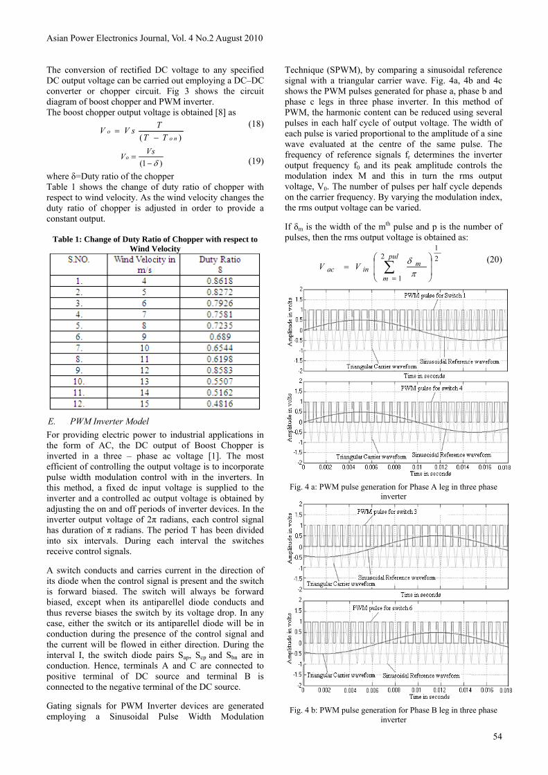
where δ=Duty ratio of the chopper Table 1 shows the change of duty ratio of chopper with respect to wind velocity. As the wind velocity changes the duty ratio of chopper is adjusted in order to provide a constant output.
Table 1: Change of Duty Ratio of Chopper with respect to Wind Velocity
E. PWM Inverter Model For providing electric power to industrial applications in the form of AC, the DC output of Boost Chopper is inverted in a three – phase ac voltage [1]. The most efficient of controlling the output voltage is to incorporate pulse width modulation control with in the inverters. In this method, a fixed dc input voltage is supplied to the inverter and a controlled ac output voltage is obtained by adjusting the on and off periods of inverter devices. In the inverter output voltage of 2π radians, each control signal has duration of π radians. The period T has been divided into six intervals. During each interval the switches receive control signals. A switch conducts and carries current in the direction of its diode when the control signal is present and the switch is forward biased. The switch will always be forward biased, except when its antiparellel diode conducts and thus reverse biases the switch by its voltage drop. In any case, either the switch or its antiparellel diode will be in conduction during the presence of the control signal and the current will be flowed in either direction. During the interval I, the switch diode pairs Sap, Scp and Sbn are in conduction. Hence, terminals A and C are connected to positive terminal of DC source and terminal B is connected to the negative terminal of the DC source. Gating signals for PWM Inverter devices are generated employing a Sinusoidal Pulse Width Modulation
Technique (SPWM), by comparing a sinusoidal reference signal with a triangular carrier wave. Fig. 4a, 4b and 4c shows the PWM pulses generated for phase a, phase b and phase c legs in three phase inverter. In this method of PWM, the harmonic content can be reduced using several pulses in each half cycle of output voltage. The width of each pulse is varied proportional to the amplitude of a sine wave evaluated at the centre of the same pulse. The frequency of reference signals fr determines the inverter output frequency f0 and its peak amplitude controls the modulation index M and this in turn the rms output voltage, V0. The number of pulses per half cycle depends on the carrier frequency. By varying the modulation index, the rms output voltage can be varied. If δm is the width of the mth pulse and p is the number of pulses, then the rms output voltage is obtained as:
21
2
1⎟⎟
⎠
⎞
⎜⎜
⎝
⎛= ∑
=
pul
m
minac VV
πδ
(20)
Fig. 4 a: PWM pulse generation for Phase A leg in three phase
inverter
Fig. 4 b: PWM pulse generation for Phase B leg in three phase
inverter
R. Bharanikumar et.al: Modeling and Simulation…..
55
Fig. 4 c: PWM pulse generation for Phase C leg in three phase
inverter
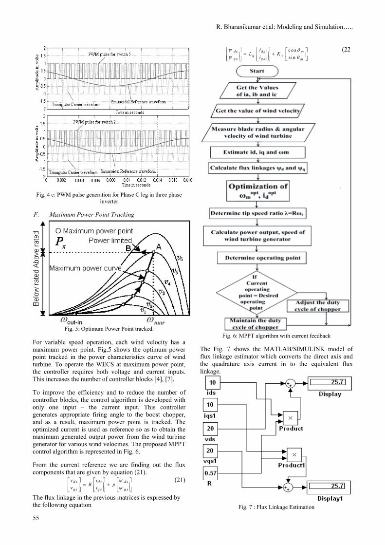
F. Maximum Power Point Tracking
Fig. 5: Optimum Power Point tracked.
For variable speed operation, each wind velocity has a maximum power point. Fig.5 shows the optimum power point tracked in the power characteristics curve of wind turbine. To operate the WECS at maximum power point, the controller requires both voltage and current inputs. This increases the number of controller blocks [4], [7]. To improve the efficiency and to reduce the number of controller blocks, the control algorithm is developed with only one input – the current input. This controller generates appropriate firing angle to the boost chopper, and as a result, maximum power point is tracked. The optimized current is used as reference so as to obtain the maximum generated output power from the wind turbine generator for various wind velocities. The proposed MPPT control algorithm is represented in Fig. 6. From the current reference we are finding out the flux components that are given by equation (21).
d s d s d s
q s q s q s
v iR p
v iψψ
⎡ ⎤ ⎡ ⎤ ⎡ ⎤= +⎢ ⎥ ⎢ ⎥ ⎢ ⎥
⎢ ⎥ ⎢ ⎥ ⎢ ⎥⎣ ⎦ ⎣ ⎦ ⎣ ⎦
(21)
The flux linkage in the previous matrices is expressed by the following equation
c o ss in
d s d s t mq e
q s q s t m
iL K
iψ θψ θ⎡ ⎤ ⎡ ⎤ ⎡ ⎤
= +⎢ ⎥ ⎢ ⎥ ⎢ ⎥⎢ ⎥ ⎢ ⎥ ⎣ ⎦⎣ ⎦ ⎣ ⎦
(22
Fig. 6: MPPT algorithm with current feedback
The Fig. 7 shows the MATLAB/SIMULINK model of flux linkage estimator which converts the direct axis and the quadrature axis current in to the equivalent flux linkage.
Fig. 7 : Flux Linkage Estimation
Asian Power Electronics Journal, Vol. 4 No.2 August 2010
56
In the MPPT algorithm as shown in Fig. 5 the values of ia, ib and ic is taken as input and id , iq and ωm are calculated using the equations (23),(24) and (25),
(2 / 3)( sin sin( ) sin( ))d a b ci i i t i tθ θ ω θ ω= + − + + (23)(2 / 3)( cos cos( ) cos(q a b ci i i t iθ θ ω θ= + − + + ))tω (24)
2 rm
np Gω
ω = (25)
The value of flux linkages are obtained by using equations (26) and (27),
d ds dsv Riψ = + (26)
q qs qsv Riψ = + (27)
The optimized speed is given by equation (28), 3 2 2
0 2 1 12
1(( )3 )) ( * )3
optm rc k k k k v
kω = − + −
(28)
Tip speed ratio (λ) and power output are obtained from the equations (1) and (2), given in the wind turbine model. For a particular wind velocity, the current operating point is determined by using the power-speed relationship and the desired operating point is determined by using the optimized value. If current operating point is equal to desired operating point then the duty cycle of chopper is maintained as the same otherwise the duty cycle of chopper is adjusted to make to make both operating points equal and again the process is repeated.
V. MATLAB IMPLEMENTATIONLM) Fig. 8 shows the overall simulation model of Wind Energy Conversion System. This model is simulated in MATLAB/SIMULINK for various wind velocities.
Fig. 8: MATLAB model of Wind Energy Conversion System
VI. RESULTS
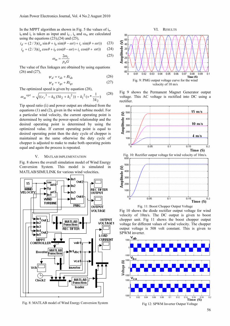
Fig. 9: PMG output voltage curve for the wind
velocity of 10 m/s
Fig 9 shows the Permanent Magnet Generator output voltage. This AC voltage is rectified into DC using a rectifier.
Fig. 10: Rectifier output voltage for wind velocity of 10m/s.
Fig. 11: Boost Chopper Output Voltage
Fig 10 shows the diode rectifier output voltage for wind velocity of 10m/s. The DC output is given to boost chopper unit. Fig 11 shows the boost chopper output voltage for different values of wind velocity. The chopper output voltage is 508 volt constant. This is given to SPWM inverter.
Fig 12: SPWM Inverter Output Voltage
R. Bharanikumar et.al: Modeling and Simulation…..
57
Fig. 13: Sinusoidal Output Voltage of SPWM Inverter
Figs 12 and 13 show the inverter output voltage of 415Volt AC is constant for that all wind velocities. This is given to load.
Fig 14: Duty cycle variation for variation in wind velocity
Fig 15: Maximum Power Point Tracking
Fig. 16: Optimum Power Trajectory
Fig. 14 shows the variation in duty cycle for different values of wind velocity. As the wind velocity is varied, the
duty cycle of chopper varies accordingly to maintain operation of WECS at maximum power point. Fig 15 shows the maximum power point tracked for different values of wind velocity. Fig 16 shows the optimum power trajectory. The maximum power point for various wind velocities are tracked in the graph.
Fig. 17: Optimum Torque Trajectory
Fig 17 shows the Optimum Torque Trajectory of the wind turbine generator model. From the above two figures the maximum power and torque points for each wind velocity can be determined.
VII. CONCLUSION The variable-speed wind energy conversion system using a permanent magnet generator has been discussed in this paper and the optimal control strategy of PMG maximizing the generated power was proposed. The optimum current value that maximizes output power is determined and used as reference for MPPT algorithm. Also MPPT control is achieved without a wind speed sensor. The control algorithm is made simple from other existing algorithms by this current reference. The system configuration is also simple, but the operation of wind turbine generator is optimized. Simulation study on a Wind Energy Conversion System employing MATLAB/SIMULINK model is the core coverage in this paper.
APPENDIX PMG - 0.75kW, 380V, 1000rpm Converter unit -500V, 10A Load - 3 phase, 415V, 10A
REFERENCES [1] Yaow-Ming Chen,Yuan-Chuan Liu, Shih-Chieh Hung and
Chung-Sheng Cheng, “Multi-Input Inverter for Grid-Connected Hybrid PV/Wind Power System” , IEEE Tansactions on Power Electronics, Vol. 22. No. 3, May 2007, pp. 1070-1077.
[2] Monica Chinchilla, Santiago Arnaltes and Juan Carlos Burgos, “Control of Permanent-Magnet Generators Applied to Variable-Speed Wind-Energy Systems connected to the Grid”, IEEE Transactions on Energy Conversion, Vol. 21, No. 1, March 2006, pp. 130-135.
[3] P. Anandavel, K. Rajambal and C. Chellamuthu, “Power optimization in a Grid-connected wind energy conversion system”, IEEE Conf. PEDS 2005, pp.1617-1621.

Asian Power Electronics Journal, Vol. 4 No.2 August 2010
58
[4] ShigeoMorimoto, Hideaki Nakayama, Masayuki Sanada, Yoji Takeda,“Sensorless Output Maximization Control for Variable Speed Wind Generation System using IPMSG”, IEEE Transactions on Industry Applications, Vol. 41, No. 1, Jan/Feb 2005, pp. 60-67.
[5] Kelvin Tan, Syed Islam“Optimum Control Strategies in Energy Conversion of PMSG Wind Turbine System without Mechanical Sensors”, IEEE Transactions on Energy Conversion, Vol. 19, No. 2, June 2004, pp. 392-399.
[6] A.B. Raju, K.Chatterjee and B.G. Fernandes, “A Simple Power Point Tracker for Grid connected Variable Speed Wind Energy Conversion System with reduced Switch Count Power Converters”, IEEE Power Electronics Specialist Conference, Vol. 2, 2003. pp. 748-753.
[7] Jia Yaoqin, Yang Zhongqing and Cao Binggang, “A New Maximum Power Point Tracking Control Scheme for Wind Generation”, IEEE Power System Technology, Proceedings, Conferences, Vol. 1, pp. 144-148.
[8] Kenji Amei, Yukichi Takayasu, Takahisa Ohji and Masaaki Sakui, “A Maximum Power Control of Wind Generator System using a Permanent Magnet Synchronous Generator and a Boost Chopper Circuit”, PCC-Osaka Vol. 3, 2002, pp.1477- 1452.
[9] N. Yamamura, M. Ishida and T.Hori, “A Simple Wind Power Generating System with Permanent Magnet Type Synchronous Generator”, IEEE Conf. PEDS’99, Vol. 2, pp.849- 854.
BIOGRAPHIES R. Bharanikumar was born in Tamilnadu, India, on May 30, 1977. He received the B.E degree in Electrical and Electronics Engineering from Bharathiyar University, in 1998. He received his M.E Power Electronics and Drives from College of Engineering Guindy Anna University in 2002. He has 9 yrs of teaching experience. Currently he is working as Asst. Professor in EEE department, Bannari Amman Institute of Technology, Sathyamangalam,
TamilNadu, India. Currently he is doing research in the field of power converter for wind energy conversion system, vector controller for synchronous machine drives.
A. C. Yazhini was born on Nov14, 1984. She received her B.E Degree in Electrical and Electronics Engineering from V.L.B. Janakiammal College of Engineering and Technology, Coimbatore, Anna University. She completed M.E in Power Electronics and Drives at Bannari Amman Institute of Technology, affiliated to Anna University. She is working as Lecturer in EEE department, Bannari Amman Institute of Technology, Sathyamangalam, TamilNadu,
India. Her current research is in the field of controller for PMG and ZSI.
A. Nirmal Kumar was born in the year 1951. He completed his PG and UG in Electrical Engineering from Kerala and Calicut University respectively. He completed PhD in Power Electronics in the year 1992 from P.S.G. College of Technology, Coimbatore under Bharathiar University. He was with N.S.S. College of Engineering for nearly 28 years in various posts before joining Bannari Amman Institute of Technology, Sathyamangalam,
TamilNadu, India in the year 2004. He is a recipient of Institution of Engineers Gold Medal in the year 1989. His current research areas include Power converters for Wind Energy Conversion System and Controller for Induction motor drives.

Narayanappa et.al: Improvemed Power Quality…..
59
Improvemed Power Quality Using Photovoltaic Unified Static Compensation Techniques
Narayanappa1 K. Thanushkodi2
Abstract - This paper describes the design and simulation of custom power controller photovoltaic based power electronic device used for mitigations in voltage sag, swells and reactive power compensation and also controlled current harmonics. This system increases efficiency when compared to the conventional power distribution system. A new PWM based control scheme is performed by using digital simulator PSCAD/EMTDC.4.2 and the simulation was carried out. The simulation results prove the capability of the photovoltaic based system in mitigating voltage sag, flicker reduction and voltage unbalanced mitigation in a power distribution system. Keywords - Voltage sag, custom power, PVUC, PSCAD/EMDC, photovoltaic cells.
I. INTRODUCTION In recent years power quality issues have become more and more important both in practice and in research. Power quality can be considered to be the proper characteristics of supply voltage and also a reliable and effective process for delivering electrical energy to consumers. Binding standards and regulations impose on suppliers and consumers, the obligation to keep required power quality parameters at the point of common coupling (PCC). Interest in power quality issues results not only from the legal regulations but also from growing consumer demands. Owing to increased sensitivity of applied receivers and process controls, many customers may experience severe technical and economical consequences of poor power quality. Disturbances such as voltage fluctuations, flicker, or imbalance can prevent appliances from operating properly and make some industrial processes shut down. On the other hand, such phenomena now appear more frequently in the power system because of systematic growth in the number and power of nonlinear and frequently time variable loads. When good power quality is necessary for technical and economical reasons, some kind of disturbance compensation is needed and that is why applications of power quality equipment have been increasing.
II. OPERATION OF PHOTOVOLTAIC UNIFIED OMPENSATION (PVUC)
The general structure of the Photovoltaic Unified Compensation (PVUC) contains two "back to back" voltage source converters using Insulated-Gate-Bipolar Transistor (IGBT) with a common DC link in Fig.1. Shunt converter is connected as parallel and another converter is series with distribution system. The paper first received 9 Nov2009 and in revised form 18 Mar 2010. Digital Ref: Digital Ref: A170701257 1 Department of Electrical Engineering, Adhiyamaan college of
Engineering, Anna University, Email:[email protected]
2 Director in ACET, Anna University, Coimbatore, Email: [email protected]
The shunt converter is used to provide active power demanded by the series converter through a common DC link. The series converter provides the main function of the PVUC by injecting an AC voltage with controllable magnitude and phase angle. To the Distribution system through series converter and it exchanges the active and reactive power with the AC system. Since the converters are connected to a common DC link, they exchange only active power and there is no reactive power between them. It means that reactive power can be controlled independently at both converters. The Fig.1 enables voltage control by the shunt inverter and the series inverter controls active and reactive power.
Fig.1: Diagram of the photovoltaic unified compensator. In the shunt branch of PVUC the controlled by the phase angle of the converter and output voltage. In the series branch of PVUC the active and reactive power in the transmission line are influenced by the amplitude as well as phase angle of the injected voltage. Therefore the active power controller indicated with the reactive power and vice versa. In order to improve the interaction between the active and reactive power control, by decoupled control algorithm based on d-q axis theory was used [8,9]. Photovoltaic models have been presented by several authors [8, 6]. The PVUC model consists of a controllable voltage source connected in series with the Distribution system and two current sources added in shunt. The present model is connected in series and shunt with Distribution system.
III. CONTROL STRATEGY OF PVUC
The control system of PVUC has two parts and is described in the following subsections. A. Control system of shunt Inverter The controlling magnitude and phase of line voltage and power flow can be controlled. By the PV array supplies the voltage and inverter injected voltage to the distribution system shown Fig 2. The design of controllers for shunt and series inverter as follows.
Asian Power Electronics Journal, Vol. 4 No.2 August 2010
60
The inverter output voltage represented by in three phase system as follows.
nNkNkn vvv −= k= a, b, c
nNaNan vvv −= similarly b and c phases.
(1)
Each phase voltage can be written as:
dtdi
Lvv CkcSkkn −=
(2)
In a three phase, three wire system voltage represent with respect neutral:
( )cNbNaNnN vvvv ++=31
(3)
Substituting nNV in equation (1)
cNbNaNn vvvv31
31
32
1 −−= (4)
Similar equation can be written for phase b and c. The phase voltage can be also written as:
[ ]1
2
3
2 1 13 3 31 2 13 3 31 1 23 3 3
an
bn
cn
v Tv V T
Tv
⎡ ⎤− −⎢ ⎥⎡ ⎤ ⎡ ⎤⎢ ⎥⎢ ⎥ ⎢ ⎥⎢ ⎥= − −⎢ ⎥ ⎢ ⎥⎢ ⎥⎢ ⎥ ⎢ ⎥⎢ ⎥ ⎣ ⎦⎣ ⎦
⎢ ⎥− −⎢ ⎥⎣ ⎦
(5)
The variables Tk represent the states of inverter switches operation. Tk is ‘0’ for open the Switches and ‘1’ for closed the Switches. Defining the d k switching state function.
2 1 11 1 2 13
1 1 2
a a
b b
c c
d Td Td T
− −⎡ ⎤ ⎡ ⎤⎡ ⎤⎢ ⎥ ⎢ ⎥⎢ ⎥= − −⎢ ⎥ ⎢ ⎥⎢ ⎥⎢ ⎥ ⎢ ⎥⎢ ⎥− −⎣ ⎦⎣ ⎦ ⎣ ⎦
(6)
Converter devices voltage represents.
( )1dca Ca b Cb c Cc
idv T i T i T idt C C
= = + + (7)
The system model is complete in the ‘abc’ reference equation (8) in Fig 3.
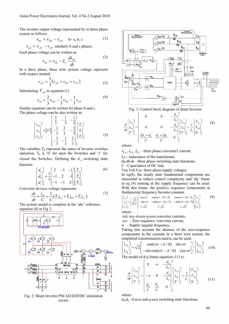
Fig. 2: Shunt Inverter PSCAD/EMTDC simulation
circuit.
Fig. 3: Control block diagram of shunt Inverter.
1
2
0 0
10 00
2 2 0
a
CCa Ca S
aCb Cb S
C c
a b a b
dLi i Vdd i i V
dt L LV V
d d d dC C
⎡ ⎤−⎢ ⎥⎢ ⎥⎡ ⎤ ⎡ ⎤ ⎡ ⎤⎢ ⎥⎢ ⎥ ⎢ ⎥ ⎢ ⎥= − +⎢ ⎥⎢ ⎥ ⎢ ⎥ ⎢ ⎥⎢ ⎥⎢ ⎥ ⎢ ⎥ ⎢ ⎥⎣ ⎦ ⎣ ⎦ ⎣ ⎦⎢ ⎥+ +⎢ ⎥⎣ ⎦
(8)
where:
Cai , Cbi , Cci - three phase converter1 current, Lc - inductance of the transformer, da,db,dc - three phase switching state functions, C - Capacitance of DC link, Vsa,Vsb,Vsc- three phase supply voltages. In eq(8), the steady state fundamental components are sinusoidal to reduce control complexity and ‘dq’ frame in eq (9) rotating at the supply frequency can be used. With this frame, the positive sequence components at fundamental frequency become constant.
cos cos( 2 / 3) cos( 2 / 3)2 sin sin( 2 / 3) sin( 2 / 3)3
1/ 2 1/ 2 1/ 2
cd ca
cq cb
co cc
i wt wt wt ii wt wt wt ii i
π ππ π
⎡ ⎤− +⎡ ⎤ ⎡ ⎤⎡ ⎤ ⎢ ⎥⎢ ⎥ ⎢ ⎥= − − − − +⎢ ⎥ ⎢ ⎥⎢ ⎥ ⎢ ⎥⎣ ⎦ ⎢ ⎥⎢ ⎥ ⎢ ⎥⎣ ⎦ ⎣ ⎦⎣ ⎦
(9)
where: icd, icq -d-axis q-axis converter currents, ico - Zero sequence converter current, w - Supply angular frequency, Taking into account the absence of the zero-sequence components in the currents in a three wire system, the simplified transformation matrix can be used.
⎥⎦
⎤⎢⎣
⎡⋅⎥
⎦
⎤⎢⎣
⎡−−
−=⎥
⎦
⎤⎢⎣
⎡
Cb
Ca
Cq
Cd
ii
wtwtwtwt
ii
cos)6/cos(sinsin)6/cos(
2π
π (10)
The model of d-q frame equation (11) is:
0
10
00
d
CCd Cd Sd
qCq Cq Sq
C c
qd
dwL
i i Vdd i w i V
dt L LV V
ddC C
⎡ ⎤−⎢ ⎥⎢ ⎥⎡ ⎤ ⎡ ⎤ ⎡ ⎤⎢ ⎥⎢ ⎥ ⎢ ⎥ ⎢ ⎥= − − +⎢ ⎥⎢ ⎥ ⎢ ⎥ ⎢ ⎥⎢ ⎥⎢ ⎥ ⎢ ⎥ ⎢ ⎥⎣ ⎦ ⎣ ⎦ ⎣ ⎦⎢ ⎥⎢ ⎥⎣ ⎦
(11)
where: dd,dq –d-axis and q-axis switching state functions,

Narayanappa et.al: Improvemed Power Quality…..
61
Vsd,Vsq-d-axis an dq-axis supply voltages. The equation (11) changes in to the current equation models.
SddCqCcd
C VdViwLdt
diL +−= ...
(12)
SqqCdCcq
C VdViwLdt
diL +−−= ... (13)
Define SddCqCd VdViwLu +−= ... (14)
SqqCdCq VdViwLu +−−= ... (15)
and considering that the current control is realized by using PI controller, the equations (16) and (17) using in Fig. 3.
. .Sd C Cq dd
v L w i ud
V− −
= (16)
. .Sq C C d qv L w i udq
V− −
= (17)
The voltage equation in the model (13) can be written as:
.d C d q C qdvC d i d id t
= + (18)
. .p v d C d q C qu d i d i= + (19)And considering that voltage control is realized by using a PI controller, the equation (20) using in Fig. 3 is:
23 supdcr pv
Vi uV
= (20)
B. Control system of series inverter The voltage compensator is a system based on power electronics inverter injected voltage and compensate the voltage sags, and keeping the load voltage around its rated value Fig 4. Under balanced condition the series inverter output voltage The variables 2kT represent the
states of series inverter operation of switches. 2kT is ‘0’ for open the Switches and ‘1’ for the closing the Switches. Defining the kd as switches state function.
2 2
2 2
2 2
2 1 11 1 2 13
1 1 2
a a
b b
c c
d Td Td T
− −⎡ ⎤ ⎡ ⎤⎡ ⎤⎢ ⎥ ⎢ ⎥⎢ ⎥= − −⎢ ⎥ ⎢ ⎥⎢ ⎥⎢ ⎥ ⎢ ⎥⎢ ⎥− −⎣ ⎦⎣ ⎦ ⎣ ⎦
(21)
The filter output voltage is
( )1kofk Lk
f
dv i idt C
= − − (22)
The dq complete model of the system as shown Fig. 4. 2
2
10 0
10 0
1 10 0
1 10 0
d
ff
qfd fd
f ffq fq
od odld
foq oq f
Lqf f
d VwLLdi iw V
L Li idv vdt w i
Cv v C
w iC C
⎡ ⎤⎡ ⎤ −⎢ ⎥⎢ ⎥⎢ ⎥⎢ ⎥⎢ ⎥⎢ ⎥⎡ ⎤ ⎡ ⎤− −⎢ ⎥⎢ ⎥⎢ ⎥ ⎢ ⎥⎢ ⎥⎢ ⎥⎢ ⎥ ⎢ ⎥= + ⎢ ⎥⎢ ⎥⎢ ⎥ ⎢ ⎥⎢ ⎥−⎢ ⎥⎢ ⎥ ⎢ ⎥⎢ ⎥⎢ ⎥⎢ ⎥ ⎢ ⎥⎣ ⎦ ⎣ ⎦⎢ ⎥⎢ ⎥⎢ ⎥⎢ ⎥− −⎢ ⎥⎢ ⎥⎣ ⎦ ⎣ ⎦
(23)
where: Cai , Cbi , Cci three phase converter currents
Lc - inductance of the transformer, da, db, dc - three phase switching state functions, C - Capacitance of DC link, Vsa,Vsb,Vsc- three phase supply voltages. The steady state fundamental component is sinusoidal to reduce control complexity in the dq frame when rotating at the supply frequency can be used. With this fame the positive sequence components at fundamental frequency becomes constant. The current equation in the models can be written as:
202 ddfqfd VdviLu −+= ω (24)
202 qqfdfq VdviLu −+−= ω (25)
Considering that the current control is realized by using PI compensators the equations (26) and (27) using in Fig. 5.
VuiLv
d dfqfodd
22
−+=
ω (26)
VuiLv
d qfdfoqq
22
−+=
ω (27)
The voltage equation in the model (23) can be written as:
.d C d q C qdvC d i d id t
= + (28)
. .pv d Cd q Cqu d i d i= + (29)
and considering that voltage control is realized by using a PI compensator, the equations (26) and (27).
23 supdcr pv
Vi uV
= (30)
Figs 3 and 5 shows the gate pulse generator circuit of the series and shunt inverters based on SPWM technique. In the presented SPWM technique, the error signal is applied to a PI controller and the output signal of PI controller is the reference signal of the SPWM technique. Voltage sag compensate equation is
Vper-sag - Vper(pu) %Sag = -------------------- * 100
V per-sag (p u)
(31)
IV. SIMULATION RESULTS
The schematics diagrams Figs. 2 and 4 are simulated by using PSCAD/ EMTDC, The PVUC is placed in a 11 kV distribution system with static load of 2.7 MVA. The simulations are carried out and illustrate the effectiveness of the PVUC as a unified compensator for voltage regulation, voltage sag compensation, voltage flicker reduction, and voltage unbalance mitigation. Load is increased from 0.5 to 1.0 per unit as shown in Fig 6. The load voltage decreases and returns to its rated voltage due to the voltage sag compensation capability of PVUC system. Fig 7 (a).shows the line voltage sag without PVUC and the Fig 7 (b) shows that line voltage sag compensation with PVUC.
The simulation period 300ms-600ms, the load is increased by closing switch C. In this case, the voltage drops by almost 34% with respect to the reference value.

Asian Power Electronics Journal, Vol. 4 No.2 August 2010
62
At 600ms. The switch C is opened and remains so throughout the rest of the simulation the load voltage is very close to the reference value.
In this same interval A is closed and the PVUC starts operating to mitigate the voltage sag and restore the voltage back to the reference value.
The simulation also carried initially an unbalanced voltage due to two phase to ground faults that are phase A and phase C at time t = 300ms to t = 600ms. As shown in Fig 8.
a) Without PVUC.
b) With PVUC.
Fig.6: Per unit Voltage Vrms at the load point.
a) Without PVUC.
b) With PVUC.
Fig 7: Line Voltage Vab at the load point.
a) PV voltage without boost converter
b) PV voltage with boost converter
Time in sec
a) Without PVUC
Time in sec
b) With PVUC
Time in sec
c) With supply voltage of PVUC
Fig. 8: Phase faults

Narayanappa et.al: Improvemed Power Quality…..
63
V. CONCLUSION The use of computer programs in simulation of custom power controllers including photo voltaic is extremely important for the development and understanding of the power electronics based technology. The result is achieved through digital simulation which clearly shows the capability of the PVUC to mitigate the voltage sags providing a continuously variable level of shunt compensation of voltage sages and regulates the voltage a new PVUC design which incorporates PV module as a DC voltage source to mitigate voltage sags in a distribution system has been presented. The PVUC is modeled with a new feedback controller scheme to control the IGBT switches of the inverter. The output is filtered in order to mitigate the harmonics generated from switching. The PV is connected to a boost converter so as to achieve a higher output voltage for charging the capacitor efficiently. Simulation results prove that the PV is a useful alternative DC source for the PVUC.
VI. REFERENCES [1] Z .A. Zakaria, B.C .Chen M.O. Hassan and J.X Yuan
“Distribution static compensator used as custom power Equipment and its simulation Using PSCAD” Information Technology Journal, Vol 7, No. 8, pp. 1141-1148.
[2] Introduction to PSCAD/EMTDC, Manitoba HVDC Research centre, March 2000.
[3] Anaya. Lar, E. Acha, “Modeling and analysis of custom power systems by PSCAD/EMTDC” IEEE Trans Power delivery, Vol. 17, No. 1, January 2002, pp. 266-272.
[4] Math .H.J. Bollen “understanding power quality problems-voltage sags and interruption” IEEE Press, 2000, pp. 2-5.
[5] S. Kim, Gwonjongyoo. Jinsoo Song “A Bifunctional Utility connected Photovoltaic system with power factor correction and UPS facility” IEEE,PVSC Vol. 25, May 1996, pp.1363-1369.
[6] Y. Chen and O. Boon-Teck “STATCOM Based an multimodel’s of multilevel converters under multiple regulation feedback control” IEEE Trans, Power Electronics, Vol. 14, Sept 1999, pp. 959-965.
[7] Kim Hyosung and Ki Sul Seung “Compensation voltage control in dynamic voltage restorer by use of feed forward and state feedback scheme” IEEE Transaction on Power Electronics, Vol. 20, No. 5, 2005, pp. 1169-77.
[8] B. Sawir, M.R. Ghani, A. A.Zin, A.H. Yatin and H. Shaibon “VoltageSag” Malaysia Experinence, IEEE, Vol. 2, Aug 1998, pp. 18-21.
[9] Bhim Singh, Alka Adya, AP. Mittal and J.R.P. Gupta “Modelling of DSTATCOM for distribution system” International Journals of Eenrgy and Technology Policy, Vol. 4, No. 1/2, 2006, pp. 142-160.
[10] M.A. Hannan and AzahMohamed “PSCAD /EMTDC simulation of unified series- shunt compensator for power quality improvement”. IEEE Trancation on Power Delivery, Vol. 20, No. 2, April 2005, pp. 1650-1657.
[11] D.G. Cho, E.Ho. Song, “A Simple UPFC control algorithm and simulation on stationary reference frame”, ISIE Conference, Pusan, Korea, 2001, pp.1810-1815.
[12] J. Jung, M. Dai and A. Keyhani “Modeling and control of a fuel Cell Based Z-source converter,” IEE Applied Power Electronics Conference, APEC’05, Vol. 2, March 6-10, 2005, pp. 1112-1118.
BIOGRAPHIES
Narayanappa received ME, Degree in power electronics in UVCE and at presently working as Asst. Professor, Adhiyamaancollege of Engineering, Hosur.
K. Thanushkodi BE. MSc (Engg), Ph. D. He Served as Principal in Government Engineering Colleges and also as member of Research Board Anna University, presently working as Director in ACET, Coimbator.

Asian Power Electronics Journal, Vol. 4 No.2 August 2010
64
Frequency Domain Analysis of Adjustable Speed Drive Systems Based on Transfer Switching Function
V. Mohan1 J. Raja2 S. Jeevananthan3
Abstract – A frequency domain analysis (FDA) is proposed to build an accurate model of the front end rectifier and pulse width modulated (PWM) inverter in an ac-ac conversion scheme, in order to analyze the harmonic currents generated by the adjustable speed drive (ASD) systems. The harmonic currents cause detrimental effects, such as an abrupt termination of the load power or oscillations, which may impose higher stresses on all the components of the power path. The impact of the interaction between non-linear loads and the power sources need to be characterized, which necessitates the accurate model. Simulation and experimental results of the suggested approach are compared with those obtained using time domain simulation, to highlight its validity. Keywords - Frequency domain analysis, PWM inverter, transfer switching function.
I. INTRODUCTION The present day systems are powered by non-ideal sources whose output impedance is not negligible, besides most of the loads are non-linear in nature [1]. The analysis of harmonic components is an inevitable part of the study, due to the requirements of higher power quality. Numerical techniques offer a good representation of the non-characteristic waveform distortion generated by the converters. The most widely used method to calculate the harmonic components is a numerical time domain simulation method, in which the various components are analyzed by solving differential equations. The time domain methods are easy to use and allow verification of system operation under any number of different operating states. However they do not provide an analytical insight required for optimal design; besides frequency dependence cannot be accurately modeled [2-3]. An alternative method for calculating the harmonic currents of a power converter uses the Fourier series and the switching functions. With a frequency domain model, the closed loop frequency responses can be established, which will facilitate the analysis of system stability and design optimization. The frequency response test is cumbersome to perform, for systems with large time constants, as the time required for the output to reach the steady state for each frequency of the test signal is exceedingly long. However frequency domain modeling is significant for power electronic circuits, which offer a faster response. The paper first received 20 Oct 2009 and in revised form 11 Apr 2010. Digital Ref: Digital Ref: A170701250 1 Professor, E.G.S.Pillay Engineering College, Nagapattinam, INDIA, E-mail: [email protected] 2 Assistant Professor, Anna University Tirchirappalli, INDIA, E- mail: [email protected] 3 Assistant Professor, Pondicherry Engineering College, Pondicherry, INDIA, E- mail:[email protected]
Sakui et al. have proposed an analytical method to calculate the harmonic currents of three-phase rectifier with a dc filter by accounting the ac side reactance [4]. They have further improved it by including the ac side resistance for continuous and discontinuous modes of conduction [5]. Hu and Yacamini have developed another analytical method to show how harmonics are transferred in the both directions through three phase bridges [6]. Larsen et. al have proposed a three-port network and analyzed the low order harmonic interactions on HVDC systems [7]. Wood and Arrillaga have developed a three-port model and used it to predict the composite resonant frequency. The same authors have shown that HVDC rectifiers and other nonlinear power electronic switching devices are almost completely linear in frequency domain [2]. This paper presents a transfer switching function (TSF) based frequency domain analysis (FDA) for adjustable speed drive (ASD) system consisting of an uncontrolled inverter and pulse width modulated (PWM) inverter. The developed FDA results are compared with time domain analysis (TDA) and experimental results.
II. FDA OF UNCONTROLLED RECTIDIERS A typical single phase diode rectifier (SPDR) is shown in Fig 1. Generally the rectifier operates as a modulator, since its primary function is to convert the fundamental power frequency ac (50 or 60 Hz) to dc. The modulation is achieved by the alternate switching action of the diodes. The instantaneous output voltage, Vdc shown in Fig.2(c), is expressed in terms of the rectifier switching function ‘S’ and ac source voltage, Vac as in (1). Fig 2 (b) shows the TS) of the SPDR, which represents the switching of the alternate diode pairs, to connect the supply voltage to the dc-bus. This switching function operates as a frequency transfer function in that it describes the way an ac side frequency signal is transferred to the dc side [8,9,10]. The Fourier series of switching function is given in (2).
Fig. 1: Uncontrolled rectifier

V. Mohan et.al: Frequency Domain Analysis…..
65
dc acV V * S= (1)
01 1
cos( ) sin( )n nn n
S a a n t b n tω ω= =
= + +∑ ∑ (2)
As the switching function is symmetrical, the Fourier coefficients ao and an are zero and the switching function S is
1,3,..
4 sin( )n
S n tn
ωπ=
= ∑ (3)
(a) (b) (c) Fig. 2 (a): Rectifier input (b): Switching function and
(c): Rectifier output Substituting (3) in (1) gives
dc m1,3 ,..
4V sin ( ) * V sin( )n
n t tn
ω ωπ=
= ∑ (4)
m m2
2 , 4 , . . .
2 V 4 V c o s ( )1n
n tn
ωπ π =
= −−∑
(5)
The final rectifier output is given by (5) and the rectifier load side current is given by
m md c 2
2 nn = 1 ,2 ,3 . . .
2 V 4 V c o s (2 nω t )I = -πR π (4 n -1 )* Z∑ (6)
where, Z2n is the impedance offered to even order harmonic components. The rectifier source side current can also be obtained by using the same switching function (S) and the load side current, expressed as
a c d cI = I * S (7)
By substituting (6) and (3) in (7)
mac 2
n=1,3,5...
m2 2
2nn=1,2,3... n=1,3,5...
8V sin(nω t)I =nR
16V cos(2nω t) sin(nω t) - *n(4n -1)*Z
π
π
∑
∑ ∑
(8)
III. FDA OF PWM INVERTERS
The typical single-phase inverter is shown in Fig 3. The typical switching function ‘SI’ of the inverter is shown in Fig 4 (b) which is derived from comparison of sine reference and triangular carrier. Figs 4(a) and 4(b) show the inverter input and output respectively. The switching angles are found using following expressions [11].
i2P int sec , sin 0
2 2th
m a mf f
jer tion MM Mπα α+ − =
(9)
i +12P int sec , sin 0
2 2th
m a mf f
jer tion MM Mπα α− − =
The Fourier coefficients for a pair of pulse is given as 34 sin( ) sin ( ) sin ( )
4 4 4m m mn m m
nB n n
nδ δ δ
α π απ
⎡ ⎤= + − + +⎢ ⎥
⎣ ⎦ (10)
Fig. 3: Single-phase full-bridge inverter
(a) (b) (c)
Fig. 4 (a): Inverter input, (b): Switching function and (c): Inverter output
Where, mα is the starting point of the pulse and mδ is the width of each pulse. The over all switching function is given as
mp m
mI
mn=1.3.5.. m=1m
3δsinn(α + )nδ4 4S = sin( ) sin(nωt)
δn 4 -sinn( +α + )4
π π
⎡ ⎤⎢ ⎥⎢ ⎥⎢ ⎥⎢ ⎥⎣ ⎦
∑ ∑
(11)
The output of the inverter is given by Vo(t)=Vdc*SI
dc m
pm
o mn=1.3.5.. m=1
mm
4V nδsin( )
n 43δV (t) = sin(nωt)sinn(α + )
4δ
- sinn( +α + )4
π
π
⎛ ⎞⎜ ⎟⎜ ⎟⎜ ⎟⎡ ⎤⎜ ⎟⎢ ⎥⎜ ⎟⎢ ⎥⎜ ⎟⎢ ⎥⎜ ⎟⎢ ⎥⎣ ⎦⎝ ⎠
∑ ∑
(12)
The inverter output current is the ratio between the output voltage and the load resistance, expressed as
dc m
pm
o mn=1.3.5.. m=1
mm
4V nδsin( )nπR 4
3δI (t) = sin(nω t)sinn(α + )4
δ- sinn(π+α + )4
⎛ ⎞⎜ ⎟⎜ ⎟⎜ ⎟⎡ ⎤⎜ ⎟⎢ ⎥⎜ ⎟⎢ ⎥⎜ ⎟⎢ ⎥⎜ ⎟⎢ ⎥⎣ ⎦⎝ ⎠
∑ ∑
(13)
The inverter input current is obtained by using the inverter output current and the same switching function (SI), given by

Asian Power Electronics Journal, Vol. 4 No.2 August 2010
66
i o II ( t ) = I ( t ) * S (14)2
m
pdc m
mn=1.3.5.. m=1
mm
nδ4 sin( )nπ 4
V 3δ= sin(nωt)sinn(α + )R 4
δ-sinn(π+α + )
4
⎡ ⎤⎛ ⎞⎢ ⎥⎜ ⎟⎢ ⎥⎜ ⎟⎢ ⎥⎜ ⎟⎡ ⎤⎢ ⎥⎜ ⎟⎢ ⎥⎢ ⎥⎜ ⎟⎢ ⎥⎢ ⎥⎜ ⎟⎢ ⎥
⎜ ⎟⎢ ⎥⎢ ⎥⎣ ⎦⎝ ⎠⎣ ⎦
∑ ∑
(15)
IV. PROBLEM FORMULATION
It is envisaged to develop a frequency domain based model of a single phase uncontrolled rectifier and a SPFB inverter, in order to evaluate the performance of the ac-ac conversion system, suitable for variable frequency system through MATLAB simulation and FPGA based hardware implementation. The simulation results are to be validated by comparing with those obtained using time domain analysis. Besides, the analytical (FDA) and experimental results are to be compared.
V. SIMULATION RESULTS The simulation is performed on a SPWM inverter using MATLAB both in time and frequency domain for various values of Ma and Mf. However the results obtained by the analytical method are compared with those available in the time domain for Ma, 0.8 and Mf, 10.
5 (a)
5 (b)
Fig. 5 (a): Output voltage (b): Output current waveform FDA -
calculated, TDA-simulated
The results are obtained for a rectifier of load resistance of 10Ω and inductance of 0.1H. The FDA results are shifted in the Y-axis scale for clarity. Fig 5 shows the dc voltage of the rectifier. It follows that the frequency domain analysis output voltage and time domain simulation output are almost the same, but the output dc current shown in Fig 5 (b) reveals that the time domain analysis takes a longer time to reach steady state. The source side current
of the rectifier is seen in Fig 6. The output voltage of inverter and fundamental component of the output are depicted in Figs 7 (a) and (b) respectively. Fig 8 shows the simulated harmonic spectrum of the inverter output voltage. The dominant harmonic components of PWM controlled inverter are pushed to higher frequency as expected. It is seen that the inverter output current waveform is the same as that of the voltage for a resistive load.
Fig. 6: Source side current waveform of rectifier
(FDA -Calculated, TDA-simulated)
7 (a)
7 (b)
Fig. 7 (a): Output voltage and (b): Fundamental of output
(Ma= 0.8, Mf=10, Vdc=300V)
Fig. 8: Harmonic spectrum of output voltage -SPWM
Ma=0.8, Mf=15 and Vdc= 300V

V. Mohan et.al: Frequency Domain Analysis…..
67
VI. HARDWARE IMPLEMENTATION The SPWM strategy is implemented on a SPFB inverter using FPGA architecture (Xilinx-Spartan-3 xc3s400-4-pq208). The design is complied, simulated using ModelSim and finally downloaded to the device through Xilinx software. The PWM pulses are generated using TRR algorithm, in which the basic idea is to generate carrier waves of any frequency, acquired by fetching the triangular samples while the reference of any magnitude is obtained through a suitable multiplying factor [12]. The FPGA processor acquires the values of Ma, Mf, base reference wave (at Ma=1) and base carrier wave (at Mf =1) as inputs. The first step is to modify the base reference to the given Ma and obtain the actual reference wave. The base reference samples are multiplied by a transitory Ma (ten times the actual Ma) and later divided by ten. The values of the actual reference wave are stored in an array of fresh adjacent locations. The second step is to compare the reference and carrier waves. The subroutine determines the actual carrier wave from the base carrier wave. The modified sine pointer (MSP) and formed pattern pointer (FPP-where the PWM pattern is to be stored) are initialized and thereafter the carrier pointer (CP) is calculated recursively.
Fig. 9: Experimental output voltage waveform with SPWM
Fig. 10: Frequency spectrum with SPWM (Ma=0.8, Mf=15)
Fig. 9 shows the typical output waveform resulted in hardware testing. The corresponding harmonic spectrum is presented in Fig. 10. A detailed comparison of analytical and experimental results is presented in Fig.11 in terms of total harmonic distortion (THD) as a function of Ma. Tables 1 and 2 shows similar comparison for Ma=0.8 and Mf=15 highlighting the dominant harmonics. Fig 12 shows the FDA and time domain analysis results of dc link current while Fig 13 gives similar results of representative dominant harmonics.
Fig.11: Comparison of analytical (FDA) and experimental values
Fig. 12: Input current of inverter (Ma= 0.8, Mf=10, Vdc=300V,
R=10Ω)
13 (a) 19th harmonic
13 (b) 21st harmonic
Fig. 13: Dominant harmonic components of SPWM inverter (Ma= 0.8, Mf=10, Vdc=300V, R=10Ω)

Asian Power Electronics Journal, Vol. 4 No.2 August 2010
68
Table 1: THD fundamental and lower order harmonics Method THD
9%) V3 (%) V5 (%) V7 (%)
TDA 76.68 12.45 8.62 2.28 FDA 68.02 0.18 0.12 0.03
Experimental 69.68 1.45 0.62 0.28
Table 2: Comparison of carrier frequency harmonics
VII. CONCLUSION
The approach has served to develop accurate FD models of the front end rectifier and PWM inverter. The importance of switching functions has been illustrated through the analysis. The scheme has created a new dimension in the harmonic analysis of power converters. The results show that TDA is very accurate and reflects the circuit behavior right from the first cycle of its working. The frequency domain modeling has highlighted a technique by which the linear operating range of the PWM inverters can be identified. The close comparison of the simulated and implemented results reveals the superiority of the proposed method. This idea will go a long way in exploring newer variable speed techniques suitable for ac drives to meet state- of-the- art applications.
REFERENCES
[1] Uffe Borup, Prasad N. Enjeti and Frede Blaabjerg, “A new space-vector-based control method for UPS systems powering nonlinear and unbalanced loads”, IEEE Transactions on Industry Applications, Vol. 37, No. 6, November/December 2001, pp. 1864-1870.
[2] A.R. Wood and J. Arrillaga, “Composite resonance: A circuit approach to the waveform distortion dynamics of an HVDC converter”, IEEE Transactions on Power Delivery, Vol. 10, No. 4, Oct. 1995, pp. 1882-1888.
[3] A.R. Wood and J Arrillaga, “HVDC converter waveform distortion: a frequency-domain analysis”, IEE. Proc.-Gener. Transm. Distrib. Vol. 142, No. 1, Jan. 1995, pp. 88-96.
[4] Masaaki Sakui, Hiroshi Fujita and Mitsuo Shioya “A method for calculating harmonic currents of a three-phase bridge uncontrolled rectifier with dc filter”, IEEE Transactions on Industrial Electronics, Vol.36, No.3, Aug 1989, pp.434-440.
[5] Masaaki Sakui and Hiroshi Fujita, “An analytical method for calculating harmonic currents of a three-phase diode-bridge rectifier with dc filter”, IEEE Transactions on Power Electronics, Vol. 9, No. 6, 1994, pp. 631-637.
[6] Lihua Hu and Robert Yacamini, “Harmonic transfer through converters and HVDC links”, IEEE Transactions on Power Electronics, Vol. 7, No. 3, Jul, 1992, pp. 514-525.
[7] E.V.Larsen, D.H.Baker and J.C.Mciver, “Low-order Harmonic interaction on AC\DC systems”, IEEE Transactions on Power Delivery, Vol. 4, No. 1, Jan.1989, pp. 493-501.
[8] A.I. Maswood, G.Joos, P.D. Ziogas and J.F. Lindsay, “Problems and solution associated with the operation of phase-controlled rectifiers under unbalanced input voltage
conditions”, IEEE Transactions on Industry Applications, Vol. 27, No. 4, July/Aug 1991, pp.765-772.
[9] Hamish D. Liard, Simon D. Round and Richard M. Duke, “A frequency domain analytical model of an uncontrolled single phase voltage source rectifier”, IEEE Transactions on Industrial Electronics, Vol. 47, No. 3, Jun 2000, pp. 525-532.
[10] Min Chen, Zhaoming Qian and Xiaoming Yuan, “Frequency domain analysis of uncontrolled rectifiers”, Proceedings of Applied Power Electronics Conference and Exposition (APEC '04), Vol. 2, 2004, pp. 804-809.
[11] S. Jeevananthan, P. Danjayan and S.Venkatesan “SPWM-An analytical characterization, performance appraisal of power electronic simulation softwares”, proceedings of International conference on Power Electronics and Drive systems (PEDS2005), Nov.28, Dec.1 2005, pp. 681-686.
[12] S. Jeevananthan, P. Dananjayan and S.Rakesh, “A unified time ratio recursion (TRR) algorithm for SPWM and TEHPWM methods: Digital implementation and mathematical analysis”, Technical Review-Journal of Institution of Electronics and Telecommunication Engineers, Vol. 22, No. 6, January/February, 2006, pp. 423-442.
BIOGRAPHIES V. Mohan obtained his Bachelor’s degree in the area of Electrical and Electronics Engineering and did his Master’s degree in Power Electronics and Drives in the year 1995 and Nov 2001 respectively. Now he is pursuing his research in the area of Random Pulse Width Modulation at Anna University Tiruchirappalli, Tiruchirappalli,Tamil Nadu. He has around 13 years of teaching experience. Currently he is working as a Professor
in the Department of Electrical and Electronics Engineering at E.G.S.Pillay Engineering College, Nagapattinam and also heading the institution as the Principal in charge.
J. Raja obtained his Batchelor’s degree in the area of Electronics and Communication Engineering and did his Master’s in Control and Instrumentation in the year 1988 and Jan 1992 respectively. He pursued his research in the area of ATM networks. He proposed modification in the ATM switching architectures by employing coding techniques as part of his Ph.D. thesis and obtained his Ph.D. degree in the year 2003. Currently he is
guiding research scholars in the areas of Error Control Coding, Congestion Control Techniques, WSN Routing Techniques and Random Pulse width modulation. He has around 18 years of teaching experience. He has taught the courses like Digital Communication Techniques, High Performance Communication Networks, High speed Switching Architectures and Communication Switching Systems at both under graduate and post graduate level. Currently he is heading the department of Electronics and Communication Engineering at Anna University, Tirchirappalli, Tamilnadu. He has published about 11 papers in national and international journals and about 35 papers in various conferences.
S. Jeevananthan received the B.E. degree in Electrical and Electronics Engineering from MEPCO SCHLENK Engineering College, Sivakasi, India, in 1998, and the M.E. degree from PSG College of Technology, Coimbatore, India, in 2000. He completed his Ph.D. degree from Pondicherry University in 2007. Since 2001, he has been with the Department of Electrical and Electronics Engineering, Pondicherry Engineering College, Pondicherry, India, where he is an
Assistant professor. He has made a significant contribution to the PWM theory through his publications and has developed close ties with the international research community in the area. He has authored more than 50 papers published in international and national conference proceedings and professional journals. Dr.S.Jeevananthan regularly reviews papers for all major IEEE Transactions in his area and AMSE periodicals (France). He is an active member of the professional societies, IE (India), MISTE., SEMCE., and SSI.
Method
2Mf-3 V27 (%)
2Mf-1 V29 (%)
2Mf+1 V31 (%)
2Mf+3 V33 (%)
TDA 27.20 51.48 43.41 9.63 FDA 17.55 38.92 38.86 17.55 Experimental 19.20 40.48 36.41 13.63
Yanbo Che et. Al: On Closed-loop…..
69
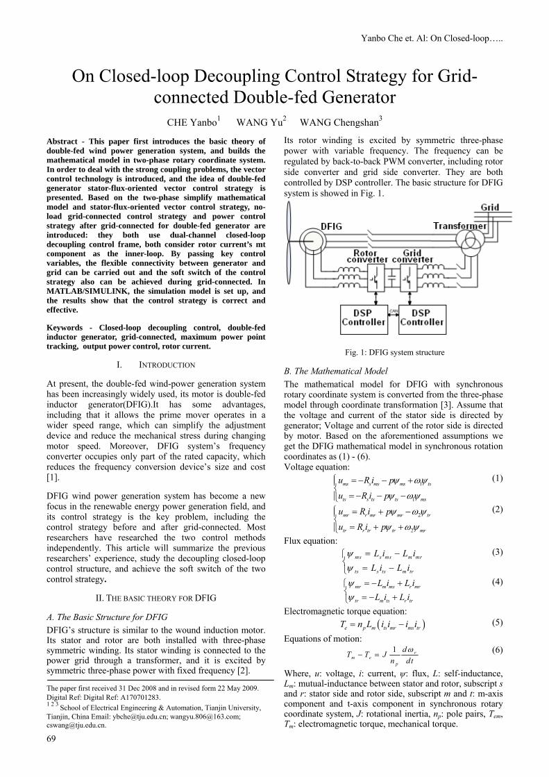
On Closed-loop Decoupling Control Strategy for Grid-connected Double-fed Generator
CHE Yanbo1 WANG Yu2 WANG Chengshan3
Abstract - This paper first introduces the basic theory of double-fed wind power generation system, and builds the mathematical model in two-phase rotary coordinate system. In order to deal with the strong coupling problems, the vector control technology is introduced, and the idea of double-fed generator stator-flux-oriented vector control strategy is presented. Based on the two-phase simplify mathematical model and stator-flux-oriented vector control strategy, no-load grid-connected control strategy and power control strategy after grid-connected for double-fed generator are introduced: they both use dual-channel closed-loop decoupling control frame, both consider rotor current’s mt component as the inner-loop. By passing key control variables, the flexible connectivity between generator and grid can be carried out and the soft switch of the control strategy also can be achieved during grid-connected. In MATLAB/SIMULINK, the simulation model is set up, and the results show that the control strategy is correct and effective. Keywords - Closed-loop decoupling control, double-fed inductor generator, grid-connected, maximum power point tracking, output power control, rotor current.
I. INTRODUCTION
At present, the double-fed wind-power generation system has been increasingly widely used, its motor is double-fed inductor generator(DFIG).It has some advantages, including that it allows the prime mover operates in a wider speed range, which can simplify the adjustment device and reduce the mechanical stress during changing motor speed. Moreover, DFIG system’s frequency converter occupies only part of the rated capacity, which reduces the frequency conversion device’s size and cost [1]. DFIG wind power generation system has become a new focus in the renewable energy power generation field, and its control strategy is the key problem, including the control strategy before and after grid-connected. Most researchers have researched the two control methods independently. This article will summarize the previous researchers’ experience, study the decoupling closed-loop control structure, and achieve the soft switch of the two control strategy.
II. THE BASIC THEORY FOR DFIG
A. The Basic Structure for DFIG DFIG’s structure is similar to the wound induction motor. Its stator and rotor are both installed with three-phase symmetric winding. Its stator winding is connected to the power grid through a transformer, and it is excited by symmetric three-phase power with fixed frequency [2]. The paper first received 31 Dec 2008 and in revised form 22 May 2009. Digital Ref: Digital Ref: A170701283. 1 2 3 School of Electrical Engineering & Automation, Tianjin University, Tianjin, China Email: [email protected]; [email protected]; [email protected].
Its rotor winding is excited by symmetric three-phase power with variable frequency. The frequency can be regulated by back-to-back PWM converter, including rotor side converter and grid side converter. They are both controlled by DSP controller. The basic structure for DFIG system is showed in Fig. 1.
Fig. 1: DFIG system structure
B. The Mathematical Model The mathematical model for DFIG with synchronous rotary coordinate system is converted from the three-phase model through coordinate transformation [3]. Assume that the voltage and current of the stator side is directed by generator; Voltage and current of the rotor side is directed by motor. Based on the aforementioned assumptions we get the DFIG mathematical model in synchronous rotation coordinates as (1) - (6). Voltage equation:
1
1
ms s ms ms ts
ts s ts ts ms
u R i p
u R i p
ψ ωψ
ψ ωψ
⎧ = − − +⎪⎨
= − − −⎪⎩
(1)
2
2
mr r mr mr tr
tr r tr tr mr
u R i p
u R i p
ψ ωψ
ψ ωψ
⎧ = + −⎪⎨
= + +⎪⎩
(2)
Flux equation: ms s ms m mr
ts s ts m tr
L i L iL i L i
ψψ
= −⎧⎨ = −⎩
(3)
mr m ms r mr
tr m ts r tr
L i L iL i L i
ψψ
= − +⎧⎨ = − +⎩
(4)
Electromagnetic torque equation: ( )e p m ts mr ms trT n L i i i i= − (5)
Equations of motion: 1 r
m ep
dT T Jn dt
ω− = (6)
Where, u: voltage, i: current, ψ: flux, L: self-inductance, Lm: mutual-inductance between stator and rotor, subscript s and r: stator side and rotor side, subscript m and t: m-axis component and t-axis component in synchronous rotary coordinate system, J: rotational inertia, np: pole pairs, Tem, Tm: electromagnetic torque, mechanical torque.
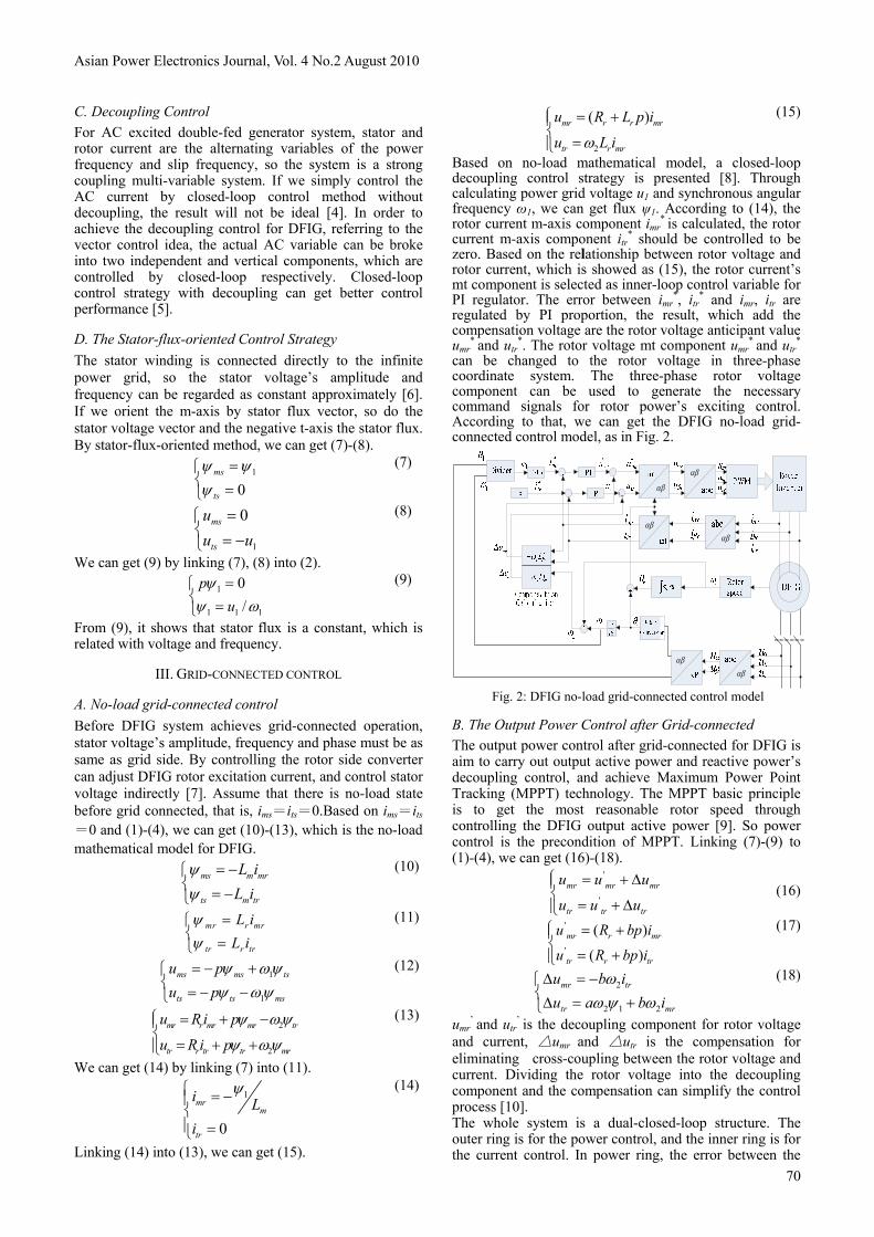
Asian Power Electronics Journal, Vol. 4 No.2 August 2010
70
C. Decoupling Control For AC excited double-fed generator system, stator and rotor current are the alternating variables of the power frequency and slip frequency, so the system is a strong coupling multi-variable system. If we simply control the AC current by closed-loop control method without decoupling, the result will not be ideal [4]. In order to achieve the decoupling control for DFIG, referring to the vector control idea, the actual AC variable can be broke into two independent and vertical components, which are controlled by closed-loop respectively. Closed-loop control strategy with decoupling can get better control performance [5]. D. The Stator-flux-oriented Control Strategy The stator winding is connected directly to the infinite power grid, so the stator voltage’s amplitude and frequency can be regarded as constant approximately [6]. If we orient the m-axis by stator flux vector, so do the stator voltage vector and the negative t-axis the stator flux. By stator-flux-oriented method, we can get (7)-(8).
1
0ms
ts
ψ ψψ
=⎧⎨ =⎩
(7)
1
0ms
ts
uu u
=⎧⎨ = −⎩
(8)
We can get (9) by linking (7), (8) into (2).
1
1 1 1
0/
pu
ψψ ω
=⎧⎨ =⎩
(9)
From (9), it shows that stator flux is a constant, which is related with voltage and frequency.
III. GRID-CONNECTED CONTROL
A. No-load grid-connected control Before DFIG system achieves grid-connected operation, stator voltage’s amplitude, frequency and phase must be as same as grid side. By controlling the rotor side converter can adjust DFIG rotor excitation current, and control stator voltage indirectly [7]. Assume that there is no-load state before grid connected, that is, ims=its=0.Based on ims=its
=0 and (1)-(4), we can get (10)-(13), which is the no-load mathematical model for DFIG.
ms m mr
ts m tr
L iL i
ψψ
= −⎧⎨ = −⎩
(10)
mr r mr
tr r tr
L iL i
ψψ
=⎧⎨ =⎩
(11)
1
1
ms ms ts
ts ts ms
u pu p
ψ ωψψ ωψ
= − +⎧⎨ = − −⎩
(12)
2
2
mr r mr mr tr
tr r tr tr mr
u R i p
u R i p
ψ ωψ
ψ ωψ
⎧ = + −⎪⎨
= + +⎪⎩
(13)
We can get (14) by linking (7) into (11).
1
0
mrm
tr
i Li
ψ⎧ = −⎪⎨⎪ =⎩
(14)
Linking (14) into (13), we can get (15).
2
( )mr r r mr
tr r mr
u R L p i
u L iω
⎧ = +⎪⎨
=⎪⎩
(15)
Based on no-load mathematical model, a closed-loop decoupling control strategy is presented [8]. Through calculating power grid voltage u1 and synchronous angular frequency ω1, we can get flux ψ1. According to (14), the rotor current m-axis component imr
* is calculated, the rotor current m-axis component itr
* should be controlled to be zero. Based on the relationship between rotor voltage and rotor current, which is showed as (15), the rotor current’s mt component is selected as inner-loop control variable for PI regulator. The error between imr
*, itr* and imr, itr are
regulated by PI proportion, the result, which add the compensation voltage are the rotor voltage anticipant value umr
* and utr*. The rotor voltage mt component umr
* and utr*
can be changed to the rotor voltage in three-phase coordinate system. The three-phase rotor voltage component can be used to generate the necessary command signals for rotor power’s exciting control. According to that, we can get the DFIG no-load grid-connected control model, as in Fig. 2.
αβ
αβ
αβ
αβ
αβ
αβ
Fig. 2: DFIG no-load grid-connected control model
B. The Output Power Control after Grid-connected The output power control after grid-connected for DFIG is aim to carry out output active power and reactive power’s decoupling control, and achieve Maximum Power Point Tracking (MPPT) technology. The MPPT basic principle is to get the most reasonable rotor speed through controlling the DFIG output active power [9]. So power control is the precondition of MPPT. Linking (7)-(9) to (1)-(4), we can get (16)-(18).
'
'
mr mr mr
tr tr tr
u u u
u u u
⎧ = + Δ⎪⎨
= + Δ⎪⎩
(16)
'
'
( )
( )mr r mr
tr r tr
u R bp i
u R bp i
⎧ = +⎪⎨
= +⎪⎩
(17)
2
2 1 2
mr tr
tr mr
u b iu a b i
ωωψ ω
Δ = −⎧⎨Δ = +⎩
(18)
umr’ and utr
’ is the decoupling component for rotor voltage and current, umr
and utr is the compensation for eliminating cross-coupling between the rotor voltage and current. Dividing the rotor voltage into the decoupling component and the compensation can simplify the control process [10]. The whole system is a dual-closed-loop structure. The outer ring is for the power control, and the inner ring is for the current control. In power ring, the error between the
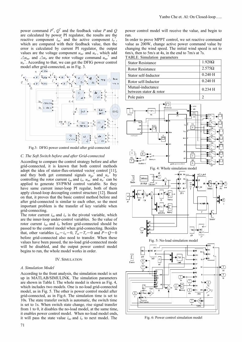
Yanbo Che et. Al: On Closed-loop…..
71
power command P*, Q* and the feedback value P and Q are calculated by power PI regulator, the results are the reactive component imr
* and the active component itr*,
which are compared with their feedback value, then the error is calculated by current PI regulator, the output values are the voltage component umr
’ and utr’, which add
umr and utr are the rotor voltage command umr
* and utr
*. According to that, we can get the DFIG power control model after grid-connected, as in Fig. 3.
rdtω∫
ddt
bricri
ari
rω
riαriβ
asu
csubsu
csibsiasi
suα
suβ
siβsiα
msu
sθ
tsimsitsu
1ψ
rθ
s rθ θ−
1ωsω
P∗
Q∗
msi∗
SP
SQ
tsi∗
1ψmri∗
tri∗
mritri
'mru
'tru
mruΔ
truΔ
mru∗
tru∗
ruα
ruβ crubruaru
Fig.3: DFIG power control model after grid-connected C. The Soft Switch before and after Grid-connected According to compare the control strategy before and after grid-connected, it is known that both control methods adopt the idea of stator-flux-oriented vector control [11], and they both get command signals umr
* and utr* by
controlling the rotor current imr and itr, umr* and utr
* can be applied to generate SVPWM control variable. So they have same current inner-loop PI regular, both of them apply closed-loop decoupling control structure [12]. Based on that, it proves that the basic control method before and after grid-connected is similar to each other, so the most important problem is the transfer of key variable when grid-connecting. The rotor current imr
and itr is the pivotal variable, which are the inner-loop under-control variables. So the value of rotor current imr
and itr before grid-connected should be passed to the control model when grid-connecting. Besides that, other variables ims=its=0, Tm=Te=0 and P=Q=0 before grid-connected also need to transfer. When these values have been passed, the no-load grid-connected mode will be disabled, and the output power control model begins to run, the whole model works in order.
IV. SIMULATION
A. Simulation Model According to the front analysis, the simulation model is set up in MATLAB/SIMULINK. The simulation parameters are shown in Table I. The whole model is shown as Fig. 4, which includes two models. One is no-load grid-connected model, as in Fig. 5. The other is power control model after grid-connected, as in Fig.6. The simulation time is set to 10s. The state transfer switch is automatic, the switch time is set to 1s. When switch state change, rise signal transfer from 1 to 0, it disables the no-load model, at the same time, it enables power control model. When no-load model ends, it will pass the state value imr
and itr to next model. The
power control model will receive the value, and begin to run. In order to prove MPPT control, we set reactive command value as 200W, change active power command value by changing the wind speed. The initial wind speed is set to 6m/s, then to 5m/s at 4s, in the end to 7m/s at 7s. TABLE. Simulation parameters
Stator Resistance 1.920Ω
Rotor Resistance 2.575Ω
Stator self-Inductor 0.240 H
Rotor self-Inductor 0.240 HMutual-inductance between stator & rotor 0.234 H
Pole pairs 2
Fig. 4: Whole simulation model
Fig. 5: No-load simulation model
Fig. 6: Power control simulation model
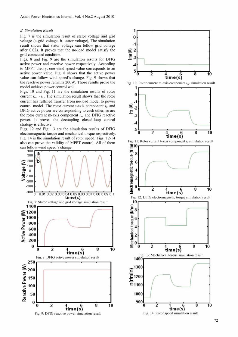
Asian Power Electronics Journal, Vol. 4 No.2 August 2010
72
B. Simulation Result Fig. 7 is the simulation result of stator voltage and grid voltage (a-grid voltage, b- stator voltage), The simulation result shows that stator voltage can follow grid voltage after 0.02s. It proves that the no-load model satisfy the grid-connected condition. Figs. 8 and Fig. 9 are the simulation results for DFIG active power and reactive power respectively. According to MPPT theory, one wind speed value corresponds to an active power value. Fig. 8 shows that the active power value can follow wind speed’s change. Fig. 9 shows that the reactive power remains 200W. Those results prove the model achieve power control well. Figs. 10 and Fig. 11 are the simulation results of rotor current imr、itr. The simulation result shows that the rotor current has fulfilled transfer from no-load model to power control model. The rotor current t-axis component itr and DFIG active power are corresponding to each other, so are the rotor current m-axis component imr and DFIG reactive power. It proves the decoupling closed-loop control strategy is effective. Figs. 12 and Fig. 13 are the simulation results of DFIG electromagnetic torque and mechanical torque respectively. Fig. 14 is the simulation result of rotor speed. Figs. 12-14 also can prove the validity of MPPT control. All of them can follow wind speed’s change.
Fig. 7: Stator voltage and grid voltage simulation result
Fig. 8: DFIG active power simulation result
Fig. 9: DFIG reactive power simulation result
Fig. 10: Rotor current m-axis component imr simulation result
Fig. 11: Rotor current t-axis component itr simulation result
Fig. 12: DFIG electromagnetic torque simulation result
Fig. 13: Mechanical torque simulation result
Fig. 14: Rotor speed simulation result

Yanbo Che et. Al: On Closed-loop…..
73
V. CONCLUSION
The simulation results show that the closed-loop decoupling control strategy on wind power generation is effective. Before grid-connected, no-load control model can satisfy grid-connected condition by controlling rotor current imr and itr. The stator voltage’s amplitude and frequency are as same as grid. When grid-connected operation happens, model can achieve the transfer for rotor current decoupling component imr and itr, and realize the soft switch between two control models. The out power control model after grid-connected can achieve active and reactive power respectively decoupling control and MPPT control also by regulating rotor current imr and itr. They both adopt closed-loop decoupling control strategy, the simulation results prove the strategy is correct and it can be applied for double-fed wind power system.
ACKNOWLEDGMENT This work is supported by Youth Foundation Project of National Natural Science Foundation Committee “Distributed Generation System Simulation and Optimization Control” (NO.50625722); National Basic Research Program of China (973 Program) “Distributed Generation Supply System Pertinent Foundational Research” (NO.2009CB219700), and National Natural Science Foundation Key Project “Key Technique Research of Distributed Generation Micro-Grid System Control and Protection” (NO. 50837001).
REFERENCES [1] T. Ackermann, L. Soder “An overview of wind energy
status 2002”, Renewable and Sustainable Energy Reviews, Vol. 6, No. 1-2, 2002, pp. 67-127.
[2] S. Muller, M. Deicke, R.W. De Doncker “Doubly Fed Induction Generator Systems for Wind Turbines”, IEEE Industry Applications Magazine, Vol. 8, No. 3, May/June 2002, pp. 26-33.
[3] R. Pena, J. C. Clare and G. M. Asher “Doubly fed induction generator using back-to-back PWM converters and its application to variable speed wind-energy generation”, IEE Proc.-Electr. Power Appl., Vol. 143, No 3, May 1996, pp. 231-241.
[4] A. Petersson, "Analysis, Modeling and Control of Doubly-Fed InductionGenerators for Wind Turbines", Chalmers Univ. Goteborg, Sweden, 2005.
[5] J. G. Slootweg, S. W. H. de Haan, H. Polinder and W. L. King “General model for representing variable speed wind turbines in power system dynamics simulations”, IEEE Trans. On Power Systems, Vol. 18, No. 1, February 2003, pp. 144-151.
[6] D. I. Kim, I. J. Ha and M. S. Ko. “Contrl of induction motor via feedback linearization with input-output decoupling”, Int. J. Contr. Vol. 51, No. 4, Mar 1990, pp. 863-883.
[7] Y. Lei, A. mullane, G. Lightbody and R. Yacamini, "Modeling of the Wind Turbine with a Doubly Fed Induction Generator for Grid Integration Studies", IEEE Transactions on Energy Conversion. Vol. 21, No. 1, 2006, pp. 257-264.
[8] Hui Li and Zhe Chen "A new current control strategy of maximizing the generated power from a doubly fed induction generator system", 12th International Power Electronics and Motion Control Conference, 2006, pp. 1557 – 1562.
[9] F. Mei and B. C. Pal, "Modeling and small-signal analysis of a grid connected doubly-fed induction generator", Proceedings of IEEE PES General Meeting 2005, San Francisco, USA, Vol. 3, 2005, pp. 2101-2108.
[10] M. Yamamoto and O. Motoyoshi "Active and reactive power control for doubly-fed wound rotor induction generator", IEEE Trans. on Power Electronics, Vol.6, No. 4, Aug. 1991. pp. 624-629.
[11] Y. Tang and L. Xu "A flexible active and reactive power control strategy for a variable speed constant frequency generating systmmm", IEEE Transactions on Power Electronics, Vol. 10, No. 4, 1995, pp. 472 -478.
[12] Nitin N. Joshi and N. Mohan "New scheme to connect DFIG to power grid", The 32nd Annual Conference of the IEEE Industrial Electronics Society, 2006, pp. 4225-4230.
BIOGRAPHIES
Che Yanbo received his B.E degree from Zhejiang University in 1993, and obtained his M.E and PhD degrees both from Tianjin University in 1996 and 2002 respectively. The major fields of study were Industrial Automation and Power System respectively. He joined in the School of Electrical Engineering & Automation, Tianjin University since 1996 and was appointed as Lecturer, Associate Professor in 1998 and 2003 respectively. Now he is the tutor of graduate students majoring in Power Electronics and
Drives. In recent years his research interests focus on the field of renewable energy, especially on the inverter technology for the micro-grid operation. He has taken charge of many projects in the field of electrical engineering and control, so far he has published over 50 papers.
Wang Yu was born on June 28th, 1984. He was form ShenYang, Liaoning Province, P.R. China. He obtained both his B.E. and M.E. degrees from School of Electrical Engineering and Automation, Tianjin University in 2007 and 2009 respectively. His research interests are all aspects of Power Electronics and Electric Drive, particularly in Doubled-fed inductor generation control.

Asian Power Electronics Journal, Vol. 4 No.2 August 2010
74
Integrated Electronic Load Controller with T-Connected Transformer for Isolated Asynchronous Generator
Bhim Singh1 V. Rajagopal2
Abstract – This paper deals with a integrated Electronic Load Controller (IELC) for an isolated asynchronous generator (IAG), used in constant power pico hydro power generation for feeding three-phase four-wire loads. The proposed IELC is used to control the voltage and frequency of IAG in the integrated manner. This IELC is realised using a T-connected transformer and three-leg insulated gate bipolar transistors (IGBTs) based current controlled voltage source converter (VSC) a capacitor, a chopper switch and an auxiliary load on its dc bus. The proposed IELC with an isolated generating system is modeled and simulated in MATLAB along with Simulink and power system blockset (PSB) toolboxes. The simulated results of IAG-IELC system are presented to demonstrate its performance for feeding three-phase four-wire linear/nonlinear (balanced/unbalanced) loads with the neutral current compensation. Keywords – Integrated electronic load controller, isolated asynchronous generator, voltage source converter, point of common coupling.
I. INTRODUCTION Conventional power generation using fossil fuels such as coal, hydrocarbons etc. cause environmental pollution and degradation. Besides, these sources are limited and at the current rate of their exploitation, are not likely to last very long. Therefore, there is need to give utmost importance to harnessing non-conventional and renewable energy sources such as wind energy, small hydro, bio-mass, solar, geothermal energy etc to reach the consumers in remote and isolated places. This leads to develop small isolated pico hydro generating plants and cost reductions may be obtained by utilizing run of the river schemes [1- 2]. The IELC (integrated electronic load controller) is used to regulate the voltage and frequency constant. Asynchronous machines like a squirrel cage type offers simple and rugged brushless rotor construction with least maintenance requirements over any conventional synchronous machines [3- 4]. As the induction machine is isolated, the reactive power for its operation may be supplied by a VAR generating unit connected across its terminals, which is generally realized in the form of capacitor banks. The capacitor banks are such selected that when driven at rated speed should produce the rated voltage at no load operating under the magnetic saturation at some stable point [5]. These IAGs have inherent voltage and frequency regulation problems in constant power applications, along with these poor voltage and frequency problems it has poor power quality [6]. Therefore, use of an IELC with a suitable scheme becomes necessary for uncontrolled pico hydro turbine driven IAG based power generation. The paper first received 21 Jan 2010 and in revised form 18 June 2010. Digital Ref: Digital Ref: A170701263 1, 2 Department of Electrical Engineering, Indian Institute of Technology, Delhi E-mail: [email protected] , [email protected]
In this paper, a synchronous reference frame theory [7-8] based control of an IELC is proposed which is having capability of controlling the voltage and frequency in integrated manner. The dc bus with this type of controller is more stable as compared to other controllers. The control scheme is fast in response as compared to any other control scheme. For controlling the voltage and frequency of IAG system, an IELC with a chopper switch and an auxiliary load at its dc bus is used. The active power of the IAG system is controlled by the chopper switch and an auxiliary load on the dc link of IELC and the reactive power is compensated by the VSC with a capacitor on the dc link. IELC acts as a reactive power compensator along with a harmonic eliminator and a load balancer a chopper switch with an auxiliary load at its DC link to absorb surplus active power not used by consumer loads. For the neutral current compensation a T-connected transformer neutral terminal can be used for non linear and unbalanced linear loads where the neutral current is compensated in primary windings of T-connected transformer keeping the VSC free from circulating currents [9-11].
II. SYSTEM CONFIGURATION AND PRINCIPLE OF OPERATION
Fig. 1 shows the system configuration of IAG, an IELC (consisting a chopper switch and an auxiliary load at its DC link and three-leg VSC with isolation T-connected transformer) and the consumer loads. A three phase capacitor bank is used for the VAR requirement of the asynchronous generator and the value of this capacitor bank is selected to generate the rated voltage at no load. The IAG generates the constant power and when consumer loads power changes, the DC chopper of IELC absorbs the difference in active power into the auxiliary load. The three-leg VSC of IELC regulates the voltage due to changes in consumer loads. Thus the voltage and frequency of IAG system is not affected and remain constant during the frequent changes in consumer loads. The IELC is connected to the IAG terminals (point of common coupling (PCC)) through a T-connected transformer and AC filtering inductors. The DC bus capacitor is used to mitigate voltage ripples and provides self supporting DC bus of VSC. Fig. 1 also shows the control strategy of an IELC for regulating constant voltage and frequency along with constant excitation capacitor of an IAG driven by uncontrolled pico hydro turbine. The control algorithm for the control of an IELC is based on the generation of reference source currents and a constant generated power of the IAG system. The T-connected transformer is used to change the voltage to an optimum level and for the neutral current compensation.

Bhim Singh et. Al: Integrated Electronic Load…..
75
III. CONTROL STRATEGY
The synchronous reference frame theory [7-8] is used for the control of the voltage and frequency of an IAG in the integrated manner. A block diagram of the control scheme along with generating system and consumer loads is shown in Fig. 1. The load currents (iLa, iLb, iLc), the terminal voltages (va, vb, vc) and dc bus voltage (vdc) of VSC are sensed as feedback signals. A. In-phase and Quadrature Component of Reference Source Currents The load currents in the three phases are converted into the d-q-0 frame using the Park’s transformation as,
L d L a
L q L b
L o L c
2 π 2 πc o sθ c o s (θ - ) c o s (θ+ )3 3i i
2 2 π 2 πi = s in θ s in (θ - ) s in (θ + ) i3 3 3
i i1 1 12 2 2
⎡ ⎤⎢ ⎥⎢ ⎥⎡ ⎤ ⎡ ⎤⎢ ⎥⎢ ⎥ ⎢ ⎥⎢ ⎥⎢ ⎥ ⎢ ⎥⎢ ⎥⎢ ⎥ ⎢ ⎥⎣ ⎦ ⎣ ⎦⎢ ⎥⎢ ⎥⎣ ⎦
(1)
A three-phase PLL (phase locked loop) is used to synchronize these signals with the terminal voltages. The d-q components are then passed through low pass filters (LPF) to extract the dc component of load currents corresponding to the active power idd and reactive power iqd. The fundamental active power component of the generator current for constant power operation can be calculated as
id* = idd+ iloss (2)
This id* is considered amplitude of an active power
component of the source current of an IAG system. The error in DC bus voltage of an IELC (Vdcer (n)) of H-bridge at nth sampling instant is as,
Vdcer(n) = Vdcref(n) – Vdc(n) (3)where Vdcref (n) is the reference DC voltage and Vdc(n) is the sensed DC link voltage of the VSC. The output of the PI controller for maintaining DC bus voltage of the VSC at the nth sampling instant is expressed as, Iloss(n) = Iloss(n-1) + Kpd Vdcer(n) – Vdcer(n-1) + Kid Vdcer(n) (4) where Iloss(n) is considered as part of active power component of source current. Kpd and Kid are the
Fig. 1: Schematic diagram of IAG with IELC and its control scheme.
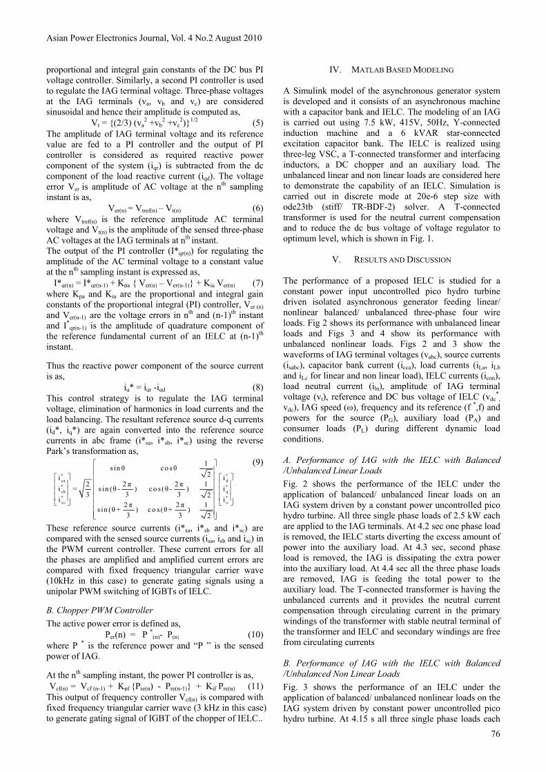
Asian Power Electronics Journal, Vol. 4 No.2 August 2010
76
proportional and integral gain constants of the DC bus PI voltage controller. Similarly, a second PI controller is used to regulate the IAG terminal voltage. Three-phase voltages at the IAG terminals (va, vb and vc) are considered sinusoidal and hence their amplitude is computed as,
Vt = (2/3) (va2 +vb
2 +vc2)1/2 (5)
The amplitude of IAG terminal voltage and its reference value are fed to a PI controller and the output of PI controller is considered as required reactive power component of the system (iqr) is subtracted from the dc component of the load reactive current (iqd). The voltage error Ver is amplitude of AC voltage at the nth sampling instant is as,
Ver(n) = Vtref(n) – Vt(n) (6)where Vtref(n) is the reference amplitude AC terminal voltage and Vt(n) is the amplitude of the sensed three-phase AC voltages at the IAG terminals at nth instant. The output of the PI controller (I*qr(n)) for regulating the amplitude of the AC terminal voltage to a constant value at the nth sampling instant is expressed as,
I*qr(n) = I*qr(n-1) + Kpa Ver(n) – Ver(n-1) + Kia Ver(n) (7)where Kpa and Kia are the proportional and integral gain constants of the proportional integral (PI) controller, Ver (n) and Ver(n-1) are the voltage errors in nth and (n-1)th instant and I*
qr(n-1) is the amplitude of quadrature component of the reference fundamental current of an IELC at (n-1)th instant. Thus the reactive power component of the source current is as,
iq* = iqr -iqd (8)This control strategy is to regulate the IAG terminal voltage, elimination of harmonics in load currents and the load balancing. The resultant reference source d-q currents (id*, iq*) are again converted into the reference source currents in abc frame (i*sa, i*sb, i*sc) using the reverse Park’s transformation as,
* *sa d* *sb q* *sc o
1s in θ c o sθ2i i
2 2 π 2 π 1i = s in (θ - ) c o s (θ - ) i3 3 3 2i i
2 π 2 π 1s in (θ+ ) c o s (θ+ )3 3 2
⎡ ⎤⎢ ⎥⎢ ⎥⎡ ⎤ ⎡ ⎤⎢ ⎥⎢ ⎥ ⎢ ⎥⎢ ⎥⎢ ⎥ ⎢ ⎥⎢ ⎥⎢ ⎥ ⎢ ⎥
⎣ ⎦ ⎣ ⎦⎢ ⎥⎢ ⎥⎢ ⎥⎣ ⎦
(9)
These reference source currents (i*sa, i*sb and i*sc) are compared with the sensed source currents (isa, isb and isc) in the PWM current controller. These current errors for all the phases are amplified and amplified current errors are compared with fixed frequency triangular carrier wave (10kHz in this case) to generate gating signals using a unipolar PWM switching of IGBTs of IELC. B. Chopper PWM Controller The active power error is defined as,
Per(n) = P *(n)- P(n) (10)where P * is the reference power and “P ” is the sensed power of IAG. At the nth sampling instant, the power PI controller is as, Vcf(n) = Vcf (n-1) + Kpf Pre(n) - Pre(n-1) + Kif Pre(n) (11)
This output of frequency controller Vcf(n) is compared with fixed frequency triangular carrier wave (3 kHz in this case) to generate gating signal of IGBT of the chopper of IELC..
IV. MATLAB BASED MODELING A Simulink model of the asynchronous generator system is developed and it consists of an asynchronous machine with a capacitor bank and IELC. The modeling of an IAG is carried out using 7.5 kW, 415V, 50Hz, Y-connected induction machine and a 6 kVAR star-connected excitation capacitor bank. The IELC is realized using three-leg VSC, a T-connected transformer and interfacing inductors, a DC chopper and an auxiliary load. The unbalanced linear and non linear loads are considered here to demonstrate the capability of an IELC. Simulation is carried out in discrete mode at 20e-6 step size with ode23tb (stiff/ TR-BDF-2) solver. A T-connected transformer is used for the neutral current compensation and to reduce the dc bus voltage of voltage regulator to optimum level, which is shown in Fig. 1.
V. RESULTS AND DISCUSSION The performance of a proposed IELC is studied for a constant power input uncontrolled pico hydro turbine driven isolated asynchronous generator feeding linear/ nonlinear balanced/ unbalanced three-phase four wire loads. Fig 2 shows its performance with unbalanced linear loads and Figs 3 and 4 show its performance with unbalanced nonlinear loads. Figs 2 and 3 show the waveforms of IAG terminal voltages (vabc), source currents (isabc), capacitor bank current (icca), load currents (iLa, iLb and iLc for linear and non linear load), IELC currents (icon), load neutral current (iln), amplitude of IAG terminal voltage (vt), reference and DC bus voltage of IELC (vdc
*,
vdc), IAG speed (ω), frequency and its reference (f *,f) and powers for the source (PG), auxiliary load (PA) and consumer loads (PL) during different dynamic load conditions. A. Performance of IAG with the IELC with Balanced /Unbalanced Linear Loads Fig. 2 shows the performance of the IELC under the application of balanced/ unbalanced linear loads on an IAG system driven by a constant power uncontrolled pico hydro turbine. All three single phase loads of 2.5 kW each are applied to the IAG terminals. At 4.2 sec one phase load is removed, the IELC starts diverting the excess amount of power into the auxiliary load. At 4.3 sec, second phase load is removed, the IAG is dissipating the extra power into the auxiliary load. At 4.4 sec all the three phase loads are removed, IAG is feeding the total power to the auxiliary load. The T-connected transformer is having the unbalanced currents and it provides the neutral current compensation through circulating current in the primary windings of the transformer with stable neutral terminal of the transformer and IELC and secondary windings are free from circulating currents B. Performance of IAG with the IELC with Balanced /Unbalanced Non Linear Loads Fig. 3 shows the performance of an IELC under the application of balanced/ unbalanced nonlinear loads on the IAG system driven by constant power uncontrolled pico hydro turbine. At 4.15 s all three single phase loads each
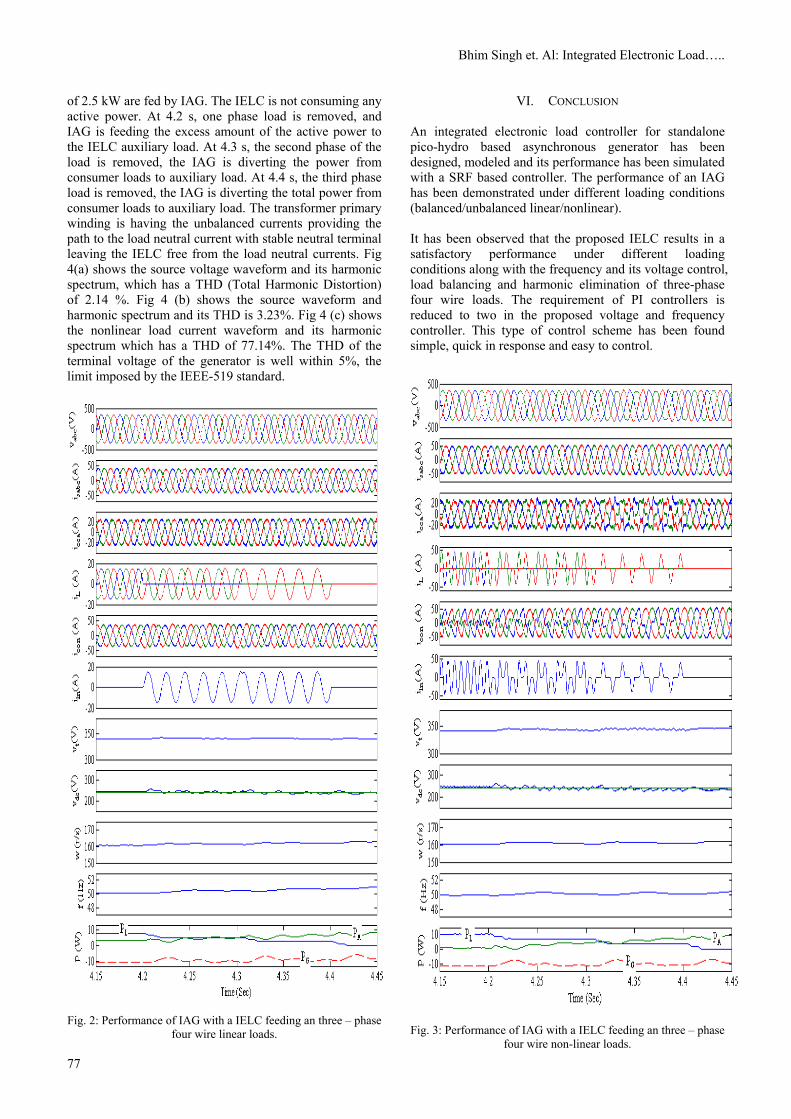
Bhim Singh et. Al: Integrated Electronic Load…..
77
of 2.5 kW are fed by IAG. The IELC is not consuming any active power. At 4.2 s, one phase load is removed, and IAG is feeding the excess amount of the active power to the IELC auxiliary load. At 4.3 s, the second phase of the load is removed, the IAG is diverting the power from consumer loads to auxiliary load. At 4.4 s, the third phase load is removed, the IAG is diverting the total power from consumer loads to auxiliary load. The transformer primary winding is having the unbalanced currents providing the path to the load neutral current with stable neutral terminal leaving the IELC free from the load neutral currents. Fig 4(a) shows the source voltage waveform and its harmonic spectrum, which has a THD (Total Harmonic Distortion) of 2.14 %. Fig 4 (b) shows the source waveform and harmonic spectrum and its THD is 3.23%. Fig 4 (c) shows the nonlinear load current waveform and its harmonic spectrum which has a THD of 77.14%. The THD of the terminal voltage of the generator is well within 5%, the limit imposed by the IEEE-519 standard.
Fig. 2: Performance of IAG with a IELC feeding an three – phase four wire linear loads.
VI. CONCLUSION An integrated electronic load controller for standalone pico-hydro based asynchronous generator has been designed, modeled and its performance has been simulated with a SRF based controller. The performance of an IAG has been demonstrated under different loading conditions (balanced/unbalanced linear/nonlinear). It has been observed that the proposed IELC results in a satisfactory performance under different loading conditions along with the frequency and its voltage control, load balancing and harmonic elimination of three-phase four wire loads. The requirement of PI controllers is reduced to two in the proposed voltage and frequency controller. This type of control scheme has been found simple, quick in response and easy to control.
Fig. 3: Performance of IAG with a IELC feeding an three – phase
four wire non-linear loads.
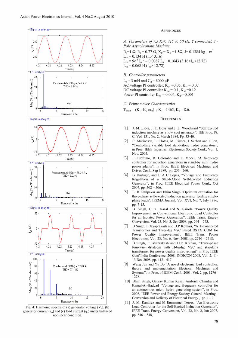
Asian Power Electronics Journal, Vol. 4 No.2 August 2010
78
Fig. 4: Harmonic spectra of (a) generator voltage (Va), (b)
generator current (isa) and (c) load current (ilb) under balanced nonlinear condition.
APPENDICES A. Parameters of 7.5 KW, 415 V, 50 Hz, Y connected, 4 - Pole Asynchronous Machine Rs=1 Ω, Rr = 0.77 Ω, Xlr = Xls =1.5Ω, J= 0.1384 kg – m2 Lm = 0.134 H (Im< 3.16) Lm = 9e-5 Im
2 – 0.0087 Im + 0.1643 (3.16<Im<12.72) Lm = 0.068 H (Im> 12.72) B. Controller parameters Lf = 3 mH and Cd = 6000 μF AC voltage PI controller: Kpa =0.05, Kia = 0.07 DC voltage PI controller Kpd = 0.1, Kid =0.12 Power PI controller Kpp = 0.004, Kip =0.001 C. Prime mover Characteristics Tshaft = (K1- K2 ωm) ; K1= 1465, K2 = 8.6.
REFERENCES
[1] J. M. Elder, J. T. Boys and J. L. Woodward “Self excited induction machine as a low cost generator”, IEE Proc. Pt. C, Vol. 131, No. 2, March 1984. Pp. 33-40.
[2] C. Marinescu, L. Clotea, M. Cirstea, I. Serban and C Ion, “Controlling variable load stand-alone hydro generators”, in Proc. IEEE Industrial Electronics Society Conf., Vol. 1, Nov. 2005.
[3] F. Profumo, B. Colombo and F. Mocci, “A frequency controller for induction generators in stand-by mini hydro power plants”, in Proc. IEEE Electrical Machines and Drives Conf., Sep 1989, pp. 256 - 260.
[4] G Dastagir, and L A C Lopes, “Voltage and Frequency Regulation of a Stand-Alone Self-Excited Induction Generator”, in Proc. IEEE Electrical Power Conf., Oct 2007, pp. 502 – 506.
[5] L. B. Shilpakar and Bhim Singh "Optimum excitation for three-phase self-excited induction generator feeding single-phase loads", IEEMA Journal, Vol. XVI, No. 7, July 1996, pp. 7-15.
[6] B. Singh, G. K. Kasal and S. Gairola “Power Quality Improvement in Conventional Electronic Load Controller for an Isolated Power Generation”, IEEE Trans. Energy Conversion, Vol. 23, No. 3, Sep 2008, pp. 764 – 773.
[7] B Singh, P Jayaprakash and D.P Kothari, “A T-Connected Transformer and Three-leg VSC Based DSTATCOM for Power Quality Improvement”, IEEE Trans. Power Electronics, Vol. 23, No. 6, Nov. 2008, pp. 2710 – 2718.
[8] B Singh, P Jayaprakash and D.P. Kothari, “Three-phase four-wire dstatcom with H-bridge VSC and star/delta transformer for power quality improvement” in Proc IEEE Conf India Conference, 2008. INDICON 2008, Vol. 2, 11-13 Dec 2008, pp. 412 - 417.
[9] Wang Jun and Yu Bo “A novel electronic load controller: theory and implementation Electrical Machines and Systems”, in Proc. of ICEM Conf. 2001, Vol. 2, pp. 1276 - 1278.
[10] Bhim Singh, Gaurav Kumar Kasal, Ambrish Chandra and Kamal-Al-Haddad “Voltage and frequency controller for an autonomous micro hydro generating system”, in Proc. 2008, IEEE Power and Energy Society General Meeting - Conversion and Delivery of Electrical Energy., pp.1 – 9.
[11] J. M. Ramirez and M Emmanuel Torres, “An Electronic Load Controller for the Self-Excited Induction Generator”, IEEE Trans. Energy Conversion, Vol. 22, No. 2, Jun 2007, pp. 546 – 548,

Bhim Singh et. Al: Integrated Electronic Load…..
79
BIOGRAPHIES
Bhim Singh was born in Rahamapur, India, in 1956. He received the B.E. degree in Electrical Engineering from University of Roorkee (Now IIT Roorkee), Roorkee, India, in 1977, and M.Tech. and Ph.D. degrees in Electrical Engineering from Indian Institute of Technology Delhi (IIT-Delhi), New Delhi, India, in 1979 and 1983, respectively. In 1983, he joined Department of Electrical Engineering, University of Roorkee, as a Lecturer, and in 1988, became a Reader. In
December 1990, he joined the Department of Electrical Engineering, IIT-Delhi, as an Assistant Professor, became an Associate Professor in 1994 and a Professor in 1997. He has received Khosla Research Prize of University of Roorkee in the year 1991. He is recipient of JC Bose and Bimal K Bose awards of The Institution of Electronics and Telecommunication Engineers (IETE) for his contribution in the field of Power Electronics in the year 2000. He is also a recipient of Maharashtra State National Award of Indian Society for Technical Education (ISTE) in recognition of his outstanding research work in the area of Power Quality in the year 2006. He has received PES Delhi Chapter Outstanding Engineer Award for the year 2006. He has been the General Chair of the IEEE International Conference on Power Electronics, Drives and Energy Systems (PEDES’2006) held in New Delhi. His current research interests include power electronics, electrical machines and drives, active filters, flexible ac transmission system (FACTS), high-voltage dc (HVDC), and power quality. Dr. Singh is a Fellow of the Indian National Academy of Engineering (INAE), the National Academy of Science, India (NASI), the Institution of Engineers (India) (IE (I)), and the Institution of Electronics and Telecommunication Engineers (IETE). He is a Life Member of the Indian Society for Technical Education (ISTE), the System Society of India (SSI), and the National Institution of Quality and Reliability (NIQR), and a Fellow of the Institute of Electrical and Electronics Engineers (IEEE).
V. Rajagopal was born in Kazipet, Warangal, India, in 1969. He received the AMIE (Electrical) degree from The Institution of Engineers (India), in 1999 and the M.Tech. degree from the Uttar Pradesh Technical University India, in 2004, His area of interest includes power electronics and drives, renewable energy generation and applications, FACTS, and power quality. He is currently working towards Ph D degree at the Department of Electrical Engineering, Indian
Institute of Technology (IIT) Delhi, India. He is a life member of the Indian Society for Technical Education (ISTE) and the Institution of Engineers (India) (IE (I)) and a Student Member of the Institute of Electrical and Electronics Engineers (IEEE).

Asian Power Electronics Journal, Vol. 4 No.2 August 2010
80

Asian Power Electronics Journal, Vol. 4 No.2 August 2010
81
A Almabouada F. 46
B Beggar R. 46Bharanikumar R. 52 C CHE Yanbo 69 J
Jeevananthan S. 64M Mohan V. 64 N Noukaz A. 46Nirmal Kumar A. 52Narayanappa 59 L Louhibi D. 46 R Raja J. 64Rajagopal V. 74 S Singh Bhim 74 T Thanushkodi K. 59
W WANG Chengshan 69WANG Yu 69
Y Yazhini A.C. 52

Asian Power Electronics Journal, Vol. 4 No.2 August 2010
82
Submission details Only online submission will be accepted. Please first register and submit online. The paper is in double column and is similar to most IET or IEEE journal format. This is no page limit. Any number of pages of more than 6 will be subject to additional charge. The paper guidelines can be downloaded using the link: http://perc.polyu.edu.hk/apejournal/ Any queries, please contact Prof. Eric Cheng, Publishing Director of APEJ, Dept. of Electrical Engineering, The Hong Kong Polytechnic University, Hung Hom, Hong Kong. Email: [email protected] Fax: +852-2330 1544 Any secretarial support and production related matters, please contact Mr. Ken Ho, Power Electronics Research Centre, The Hong Kong Polytechnic University, Hung Hom, Hong Kong. Email: [email protected] Tel: +852-3400 3348 Fax: +852-3400 3343 Publication Details The Journal will be published 3 times a year. The first issue was published in 2007. Response time for paper acceptance is within 3 months. Financial Charge All the accepted papers will be printed without charge for 6 or less pages. An additional page charge is HK$100 per page. A hardcopy of the journal will be posted to the corresponding author free of charge. Additional copies of the journal can be purchased at HK$200 each. The charge includes postage and packing. All Chinese Papers will be subjected to a translational fee of HK$350 per page. It will be charged when the paper is accepted for publication. Advertising Advertisement is welcome. Full page advertisement is HK$1000. For colour advertisement, the amount is doubled. All the advertisement will be both posted online in the journal website and hardcopy of the journal. For advertising enquiries and details, please contact Ms. Anna Chang, [email protected] . Tel: +852-3400 3348 Fax: +852-3400 3343 For payment, please send your cheque, payable to ‘The Hong Kong Polytechnic University, address to Ms. Canary Tong, Secretary of APEJ, Dept. of Electrical Engineering, The Hong Kong Polytechnic University, Hung Hom, Hong Kong.