as a high-performance lithium-ion battery supporting ... · pdf filesupporting information...
TRANSCRIPT

Supporting InformationFlexible All Inorganic Nanowire Bilayer Mesh as a High-Performance Lithium-Ion Battery Anode
Wei-Chung Chang, Tzu-Lun Kao, Yow Lin, and Hsing-Yu Tuan*
Department of Chemical Engineering, National Tsing Hua University, 101, Section 2,
Kuang-Fu Road, Hsinchu, Taiwan 30013, ROC
*Corresponding authors
Phone: (886)3-571-5131 ext:42509
Email: [email protected]
Electronic Supplementary Material (ESI) for Journal of Materials Chemistry A.This journal is © The Royal Society of Chemistry 2017
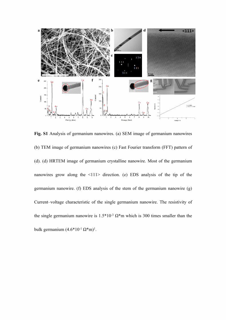
Fig. S1 Analysis of germanium nanowires. (a) SEM image of germanium nanowires
(b) TEM image of germanium nanowires (c) Fast Fourier transform (FFT) pattern of
(d). (d) HRTEM image of germanium crystalline nanowire. Most of the germanium
nanowires grow along the <111> direction. (e) EDS analysis of the tip of the
germanium nanowire. (f) EDS analysis of the stem of the germanium nanowire (g)
Current–voltage characteristic of the single germanium nanowire. The resistivity of
the single germanium nanowire is 1.5*10-3 Ω*m which is 300 times smaller than the
bulk germanium (4.6*10-1 Ω*m)1.

Fig. S2 Photographs of fabricating process of layered Ge/Cu nanowire mesh
electrode. (a) The solution of copper nanowires was dropped into a PTFE mold. (b)
Dried Cu nanowire mesh, the toluene fully evaporated. (c) The solution of germanium
nanowires was then dropped onto the copper nanowires in PTFE mold. (d) Dried
Ge/Cu nanowire mesh electrode, the toluene fully evaporated. (e), (f) The flexible

Ge/Cu nanowire mesh electrode was peeled form the PTFE mold and tailored to
adequate size for following electrochemical test or other analysis.
Fig. S3 Photographs of the mass of (a) Cu foil and (b) Cu nanowire mesh.
Fig. S4 Coulombic efficiency of layered Ge/Cu nanowire mesh electrode at the rate of
0.1 C and 1 C with FEC/DEC electrolyte.

Fig. S5 Cycling performance of the Ge nanowire mesh/Cu foil electrode at a rate of
0.1 C.

Fig. S6 Cycling performance of the Ge/Cu nanowire mesh electrode with EC/DMC
electrolyte. (a) 0.1 C. (b) 1 C.
Fig. S7 Analysis of layered Ge/Cu nanowire mesh electrode after 200 cycles at a rate
of 1 C with EC/DMC electrolyte. (a) Photograph of disassembling CR2032 coin cell.
(b) Photograph of the fragments of Ge/Cu nanowire mesh electrode. Ge/Cu nanowire
mash electrode was hard to peel from coin cell. (c) SEM image of Cu layer of layered
Ge/Cu nanowire mesh electrode. (d) SEM image of Ge layer of Ge/Cu nanowire mesh

electrode. Most of the germanium nanowires were cracked and covered with thick
SEI layer (e) High magnification SEM image of germanium nanowires. (f) TEM
image of germanium nanowires. The inset image shows the germanium nanowire with
incompact SEI layer. (g) Nyquist plots of layered Ge/Cu nanowire mesh electrode
half-cell after various cycle 1st, 15th, 30th, 50th, 100th at a rate of 1 C (1st cycle at a rate
of 0.1 C). (h) Differential capacity profile of layered Ge/Cu nanowire mesh electrode
with the initial cycle at a rate of 0.1 C and the remaining 99 cycles at a rate of 1 C.
The green arrow points out the first cycle. The red and blue arrow point out the
gradually inward curve, which means the continuous fading of the cell.

Fig. S8 Half-cell test of commercial Li(Ni0.5Co0.3Mn0.2)O2 cathode (a) Cycling
performance. (b) Voltage profile corresponding (a) 1 C = 160 mA g-1.
Table S1 Comparison of bilayer Ge/Cu nanowire mesh electrode and conventional
slurry-coating Ge nanomaterial electrodes.
MaterialsGravimetric
Capacity (only
Loading mass
(mg cm-2)
Current
rateCycle
Gravimetric
CapacityRef.

active materials mA
h g-1)
(include binder,
conductivity agent)
(mA h g-1)
(whole
electrode)
Ge/Cu mesh 832 0.5 1 C 1000 208
Graphite*** 330 12.012 1 C 1000 193
Ge NWs 940 1 1 C 50 72 2
Ge NPS 1152 0.5 1 C 200 37 3
Ge NWs 600* 1 1 C 300 64 4
Ge NTs 765 1** 1 C 10 63 5
Gr/Ge NWs 1150* 1-1.9 1 C 200 115 6
Ge/RGO/C 993 0.6 1 C 600 48. 7
3D porous Ge 1415 1** 1 C 100 116 8
C-Ge/C 896 1 1 C 120 73 9
Sn-Ge 990 0.5 1 C 100 34 10
Ge NPs 1100 1** 0.8 C 40 90 11
Ge@C/RGO 800* 1** 0.9 C 40 70 12
Ge VNWs 550 1** 0.8 C 30 45 13
Ge/C 736 1 0.1 C 20 60 14
Ge NWs 660* 0.75 ** 0.5 C 100 41 15
Ge NPs 789 1** 0.15 C 20 65 16
Ge/Cu3Ge/C 530 1** 0.1 C 50 38 17
*The estimation of graphs of literatures.
**The literature does not provide the loading mass; we assume that the loading mass
is 1 mg cm-2.
*** Assume the areal capacity of graphite is 4 mA h cm-2 and the reversible capacity
is 330 mA h g-1.
Table S2 Comparison of bilayer Ge/Cu nanowire mesh electrode and conventional
slurry-coating Si nanomaterial electrodes.

Materials
Gravimetric
Capacity
(mA h g-1 )
(only active
materials)
Loading mass
(mg cm-2)
(include binder,
conductivity
agent)
Curren
t rateCycle
Gravimetric
Capacity
(mA h g-1)
(whole electrode)
Ref.
Ge/Cu mesh 832 0.5 1 C 1000 208
Graphite*** 330 12.012 1 1000 193
Si NWs 1800 1 0.1 C 100 129 18
Si NPs 2600 0.5 0.2 C 100 56 19
Si NWs 1500 0.2 (Si) 0.05 C 30 33 20
Si NPs 1500* 1** 1 C 500 100 21
Si fabric 804 1** 0.05 C 20 82 22
Si NPs 1250* 1** 0.5 C 100 90 23
Si NPs 1160 0.2 (Si) 0.5 C 1000 25 24
Si NWs 1300* 0.1 (Si) 0.5 C 800 14 25
Si MPs 1750 0.7 (Si) 0.1 C 130 125 26
Si NPs 1600* 0.3 (Si) 0.3 C 500 52 27
Si NPs 2200 0.2 (Si) 0.2 C 100 48 28
*The estimation of graphs of literatures.
**The literature does not provide the loading mass; we assume that the loading
weight is 1 mg cm-2.
*** Assume the areal capacity of graphite is 4 mA h cm-2 and reversible capacity is 330 mA h g-1.
Table S3 Loading mass and volumetric capacities of graphite, Ge/Cu nanowire mesh and other Ge flexible electrodes.
Loading
mass of
active
materials
(mg cm-2
)
Thickness
of Cu
(μm)
Thickness
of
active
materials
(μm)
Thickness
of
whole
electrodes
(μm)
Volumetric
capacity
based on the
total volume
of
whole
electrode
Ref.

(m Ah cm-3
)
Graphite 4 10 146.6 156.6 255.3
Ge/Cu mesh 0.5~6 15 8~96.3 23~111.3 217~539
Ge@CNFs 0.291 - - 500 5.82 29
Ge@CNFs-2 0.504 - - 200 25.2 30
Ge@Graphene 1.32 - - - - 31
Ge@CNFs-3 0.404 - - - - 32
Reference1. R. A. Serway and J. W. Jewett, Physics for Scientists and Engineers with Modern
Physics, Cengage Learning, 9th edn., 2013.2. F.-W. Yuan, H.-J. Yang and H.-Y. Tuan, ACS Nano, 2012, 6, 9932-9942.3. K. C. Klavetter, S. M. Wood, Y.-M. Lin, J. L. Snider, N. C. Davy, A. M. Chockla, D. K.
Romanovicz, B. A. Korgel, J.-W. Lee, A. Heller and C. B. Mullins, Journal of Power Sources, 2013, 238, 123-136.
4. A. M. Chockla, K. C. Klavetter, C. B. Mullins and B. A. Korgel, ACS applied materials & interfaces, 2012, 4, 4658-4664.

5. M. H. Park, Y. Cho, K. Kim, J. Kim, M. Liu and J. Cho, Angewandte Chemie, 2011, 50, 9647-9650.
6. H. Kim, Y. Son, C. Park, J. Cho and H. C. Choi, Angewandte Chemie, 2013, 52, 5997-6001.
7. F.-W. Yuan and H.-Y. Tuan, Chemistry of Materials, 2014, 26, 2172-2179.8. M.-H. Park, K. Kim, J. Kim and J. Cho, Advanced Materials, 2010, 22, 415-418.9. K. H. Seng, M.-H. Park, Z. P. Guo, H. K. Liu and J. Cho, Angewandte Chemie
International Edition, 2012, 51, 5657-5661.10. M. I. Bodnarchuk, K. V. Kravchyk, F. Krumeich, S. Wang and M. V. Kovalenko,
ACS Nano, 2014, 8, 2360-2368.11. F.-S. Ke, K. Mishra, L. Jamison, X.-X. Peng, S.-G. Ma, L. Huang, S.-G. Sun and X.-D.
Zhou, Chemical Communications, 2014, 50, 3713-3715.12. D. J. Xue, S. Xin, Y. Yan, K. C. Jiang, Y. X. Yin, Y. G. Guo and L. J. Wan, Journal of
the American Chemical Society, 2012, 134, 2512-2515.13. L. P. Tan, Z. Lu, H. T. Tan, J. Zhu, X. Rui, Q. Yan and H. H. Hng, Journal of Power
Sources, 2012, 206, 253-258.14. C. Yao, J. Wang, H. Bao and Y. Shi, Materials Letters, 2014, 124, 73-76.15. M.-H. Seo, M. Park, K. T. Lee, K. Kim, J. Kim and J. Cho, Energy & Environmental
Science, 2011, 4, 425-428.16. L. C. Yang, Q. S. Gao, L. Li, Y. Tang and Y. P. Wu, Electrochemistry
Communications, 2010, 12, 418-421.17. Y. Hwa, C.-M. Park, S. Yoon and H.-J. Sohn, Electrochimica Acta, 2010, 55, 3324-
3329.18. A. M. Chockla, K. C. Klavetter, C. B. Mullins and B. A. Korgel, Chemistry of
Materials, 2012, 24, 3738-3745.19. Y.-M. Lin, K. C. Klavetter, P. R. Abel, N. C. Davy, J. L. Snider, A. Heller and C. B.
Mullins, Chem. Commun., 2012, 48, 7268-7270.20. C. K. Chan, R. N. Patel, M. J. O’Connell, B. A. Korgel and Y. Cui, ACS Nano, 2010,
4, 1443-1450.21. N. Liu, H. Wu, M. T. McDowell, Y. Yao, C. Wang and Y. Cui, Nano Lett., 2012, 12,
3315-3321.22. A. M. Chockla, J. T. Harris, V. A. Akhavan, T. D. Bogart, V. C. Holmberg, C.
Steinhagen, C. B. Mullins, K. J. Stevenson and B. A. Korgel, Journal of the American Chemical Society, 2011, 133, 20914-20921.
23. T. H. Hwang, Y. M. Lee, B.-S. Kong, J.-S. Seo and J. W. Choi, Nano letters, 2011, 12, 802-807.
24. N. Liu, Z. Lu, J. Zhao, M. T. McDowell, H. W. Lee, W. Zhao and Y. Cui, Nature nanotechnology, 2014, 9, 187-192.

25. H. Wu, G. Chan, J. W. Choi, I. Ryu, Y. Yao, M. T. McDowell, S. W. Lee, A. Jackson, Y. Yang, L. Hu and Y. Cui, Nature nanotechnology, 2012, 7, 310-315.
26. C. Wang, H. Wu, Z. Chen, M. T. McDowell, Y. Cui and Z. Bao, Nature chemistry, 2013, 5, 1042-1048.
27. H. Wu, G. Yu, L. Pan, N. Liu, M. T. McDowell, Z. Bao and Y. Cui, Nat Commun, 2013, 4, 1943.
28. N. Liu, K. Huo, M. T. McDowell, J. Zhao and Y. Cui, Scientific reports, 2013, 3, 1919.
29. W. Li, Z. Yang, J. Cheng, X. Zhong, L. Gu and Y. Yu, Nanoscale, 2014, 6, 4532-4537.
30. W. Li, M. Li, Z. Yang, J. Xu, X. Zhong, J. Wang, L. Zeng, X. Liu, Y. Jiang, X. Wei, L. Gu and Y. Yu, Small, 2015, 11, 2762-2767.
31. R. Mo, D. Rooney, K. Sun and H. Y. Yang, Nat. Commun., 2017, 8, 13949.32. C. J. Peng, L. Wang, Q. W. Li, Y. Y. Li, K. Huo and P. K. Chu, ChemElectroChem,
2017, 4, 1002-1006.