arsh environment acquisition terminal - ti.com · – for demonstration purposes of the above...
TRANSCRIPT

Harsh Environment Acquisition Terminal

2
Outline • HT electronics need • High level overview of H.E.A.T
– Description and block level diagram
• Core Devices – Key features
• Channel Content – Overview and functional description
• Detailed Analog Implementation and Sample Measurements • Additional Key Points • Summary • Acknowledgements
3
The Need for HT Electronics • Temperature requirements have been increasing within industrial, avionics,
military and oil exploration markets for the past 20 years.
• In the energy exploration sector, the need to find new oil and natural gas resources has driven the industry to drill deeper and deeper. Wells of 15,000ft to 20,000ft (4.5 – 6.1km) are increasing common with some natural gas wells researching beyond 30,000ft, 9.4km. – With nominal Earth temperature gradients of 25 °C and 30 °C per kilometer, these
deep well can reach very high temperatures.
• Today, the military standard of 125°C is simply not HOT enough. Several semiconductor companies, like Texas Instruments, are reaching out to the industry with new products manufactured to meet >175°C temperature requirements.
4
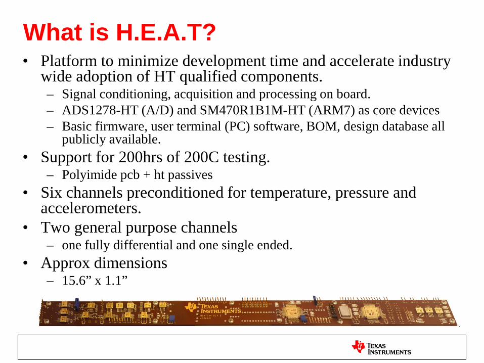
What is H.E.A.T? • Platform to minimize development time and accelerate industry
wide adoption of HT qualified components. – Signal conditioning, acquisition and processing on board. – ADS1278-HT (A/D) and SM470R1B1M-HT (ARM7) as core devices – Basic firmware, user terminal (PC) software, BOM, design database all
publicly available. • Support for 200hrs of 200C testing.
– Polyimide pcb + ht passives • Six channels preconditioned for temperature, pressure and
accelerometers. • Two general purpose channels
– one fully differential and one single ended. • Approx dimensions
– 15.6” x 1.1”
5
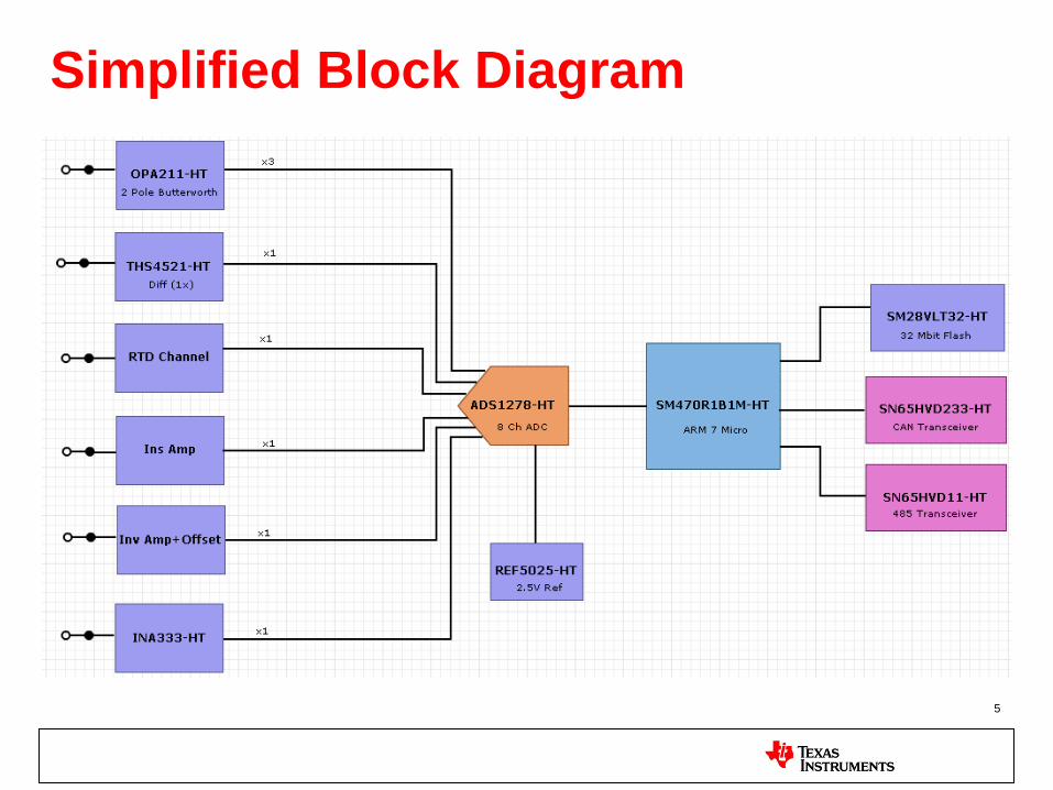
Simplified Block Diagram
6
Core Devices
• SM470R1B1M-HT – ARM7 architecture, 60 MHz system clk, 16/32-Bit RISC – On Chip 1MB flash – Flexible I/O options
• ADS1278-HT
– Up to128KSPS, Sigma Delta Architecture – High Resolution (24 bits), 17 bits enob @ 210C. – Simultaneous Sampling Capabilities, 8 Ch.
7
Featured Analog Inputs • OPA211-HT, accelerometer inputs
– All three axis inputs have a buffer amplifier with two poles in a Butterworth filter at 20Hz using the OPA211-HT
– For demonstration purposes of the above signal path we created a low temp sensor board and cabling.
• Temperature Sensing – based on the THS4521-HT and OPA2333-HT – If the on board RTD is not in place, there is a connection for a four wire
external RTD
• Pressure Sensing – A high impedance bridge amplifier using the THS4521-HT and the
OPA2333-HT to create an instrumentation amplifier. – This circuit is a high gain (251X) circuit for measuring downhole pressure – Alternatively, we are proving dedicated input with INA333-HT to be used
for pressure transducer coupling.
8
General Purpose Analog Inputs • To use the remaining two A/D inputs the following
were added – Inverting amplifier with DC offset for proper A/D dynamic
range (the user can exercise full dynamic range of A/D) • OPA211 + buffered Vref (REF5025-HT)
– One standard (1x) differential inputs using THS4521-HT.
• In addition, REF5025-HT, buffered references and other basic analog using OPA211-HT, OPA2333-HT are present in the board.

9
Firmware, interfaces and memory to uP
• Two HVD233-HT – CAN transciever (transmitter/receiver)
• One HVD11-HT – RS485 transciever (transmitter/receiver)
• In the HEAT design, a serial (SPI) interface links the ARM7 to the A/D – Basic firmware layer for A/D SPI and data relay.
10
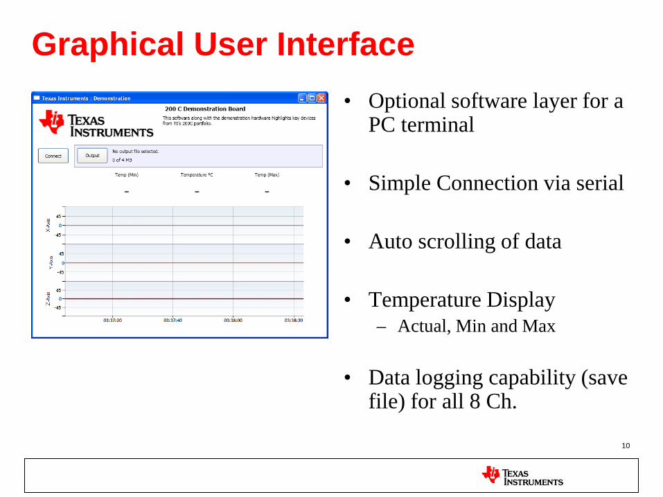
Graphical User Interface • Optional software layer for a
PC terminal • Simple Connection via serial • Auto scrolling of data • Temperature Display
– Actual, Min and Max
• Data logging capability (save file) for all 8 Ch.
11
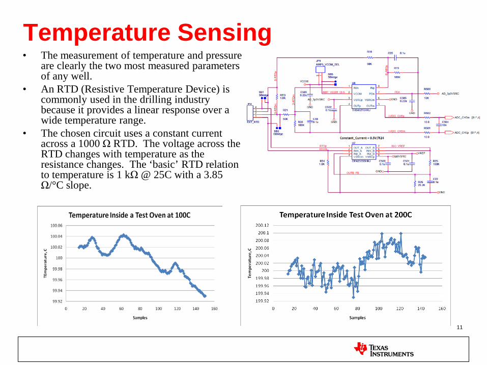
Temperature Sensing • The measurement of temperature and pressure
are clearly the two most measured parameters of any well.
• An RTD (Resistive Temperature Device) is commonly used in the drilling industry because it provides a linear response over a wide temperature range.
• The chosen circuit uses a constant current across a 1000 Ω RTD. The voltage across the RTD changes with temperature as the resistance changes. The ‘basic’ RTD relation to temperature is 1 kΩ @ 25C with a 3.85 Ω/°C slope.
12
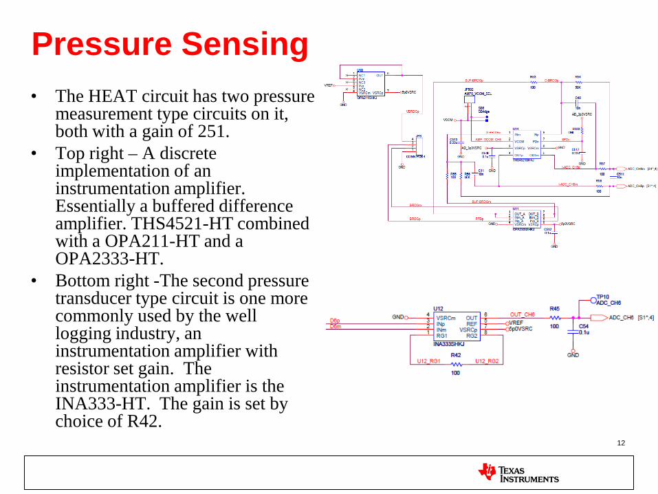
Pressure Sensing • The HEAT circuit has two pressure
measurement type circuits on it, both with a gain of 251.
• Top right – A discrete implementation of an instrumentation amplifier. Essentially a buffered difference amplifier. THS4521-HT combined with a OPA211-HT and a OPA2333-HT.
• Bottom right -The second pressure transducer type circuit is one more commonly used by the well logging industry, an instrumentation amplifier with resistor set gain. The instrumentation amplifier is the INA333-HT. The gain is set by choice of R42.
13
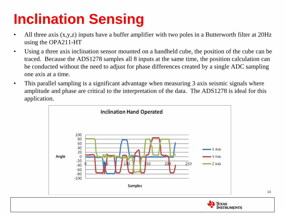
Inclination Sensing • All three axis (x,y,z) inputs have a buffer amplifier with two poles in a Butterworth filter at 20Hz
using the OPA211-HT • Using a three axis inclination sensor mounted on a handheld cube, the position of the cube can be
traced. Because the ADS1278 samples all 8 inputs at the same time, the position calculation can be conducted without the need to adjust for phase differences created by a single ADC sampling one axis at a time.
• This parallel sampling is a significant advantage when measuring 3 axis seismic signals where amplitude and phase are critical to the interpretation of the data. The ADS1278 is ideal for this application.
14
General Analog
• Fully differential path leveraging THS4521-HT into the A/D. – Ideal to get an evaluation window into the A/D. – Good for general purpose sensor evaluation.
• Inverting amplifier
– Added DC offset for dynamic input range correction into A/D
– Added a small high frequency RC filter – OPA211 + buffered Vref (REF5025-HT)
15
Power • Three main supply rails
– Five volts (5V) for analog A/D core and conditioning circuits. – Three point three volts (3.3V) for interfaces (I/O). – One point eight (1.8V) for digital cores in both A/D and processor
• Separate 1.8V rail and 3.3V rail each for A/D and ARM7 to satisfy power sequencing requirements.
• Power rails and sequencing to the HEATEVM need to be
provided externally.
16
Additional Points • Solder material type #240 (Sn95, Sb5) by Senju
• Onboard HT clocking running at 7.5 MHz
• Lifetime of 200 hrs driven by conservative de-rating of wet
tantalums capacitors.
• There is no shock testing or long term qualification in place.
• All documentation, BOM, firmware source code and design database are available.
17
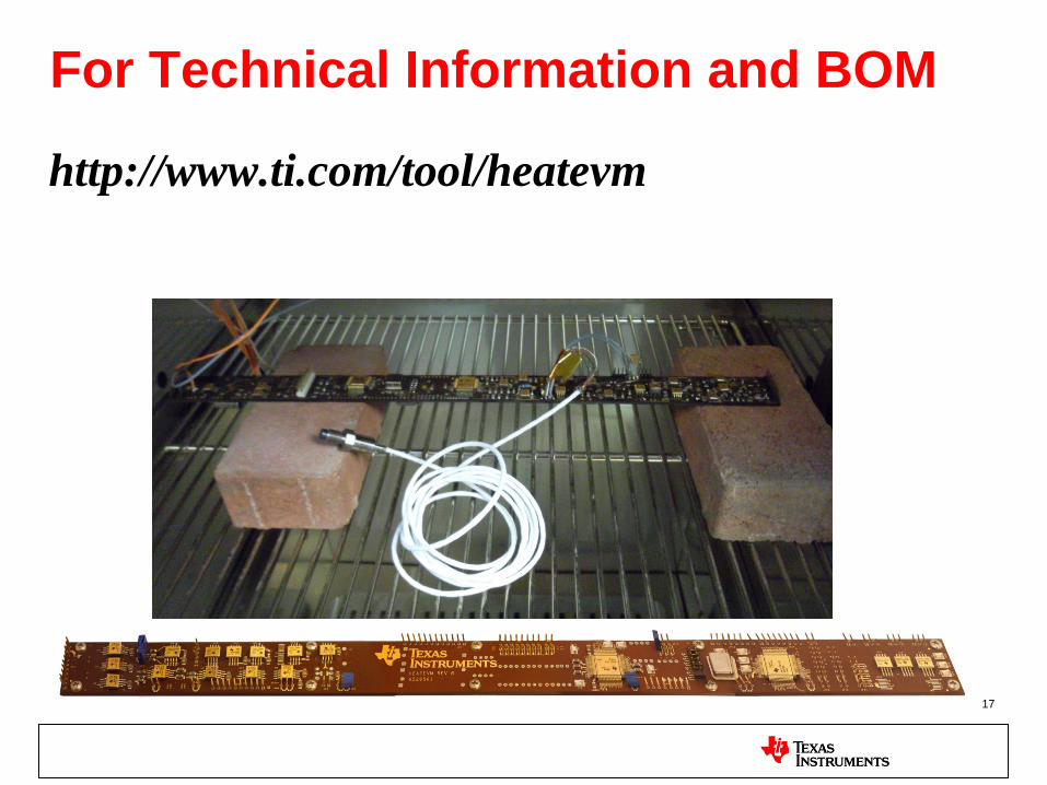
For Technical Information and BOM
http://www.ti.com/tool/heatevm
18
Closing Remarks and Summary • The HEAT circuit board is built around the SM470R1B1M-HT
(ARM7 core) microprocessor and the ADS1278-HT, A/D. – The ARM7 has a 32bit architecture, operating with a 60MHz internal core
and 1MB flash. – The ADS1278 has 8, 24 bit analog to digital converters channels
supporting simultaneous sampling.
• Pre-conditioned analog channels for a number of commonly used scenarios.
• Our main intend is to accelerate adoption of manufacturer
qualified HT components.
IMPORTANT NOTICE FOR TI REFERENCE DESIGNS
Texas Instruments Incorporated ("TI") reference designs are solely intended to assist designers (“Buyers”) who are developing systems thatincorporate TI semiconductor products (also referred to herein as “components”). Buyer understands and agrees that Buyer remainsresponsible for using its independent analysis, evaluation and judgment in designing Buyer’s systems and products.
TI reference designs have been created using standard laboratory conditions and engineering practices. TI has not conducted anytesting other than that specifically described in the published documentation for a particular reference design. TI may makecorrections, enhancements, improvements and other changes to its reference designs.
Buyers are authorized to use TI reference designs with the TI component(s) identified in each particular reference design and to modify thereference design in the development of their end products. HOWEVER, NO OTHER LICENSE, EXPRESS OR IMPLIED, BY ESTOPPELOR OTHERWISE TO ANY OTHER TI INTELLECTUAL PROPERTY RIGHT, AND NO LICENSE TO ANY THIRD PARTY TECHNOLOGYOR INTELLECTUAL PROPERTY RIGHT, IS GRANTED HEREIN, including but not limited to any patent right, copyright, mask work right,or other intellectual property right relating to any combination, machine, or process in which TI components or services are used.Information published by TI regarding third-party products or services does not constitute a license to use such products or services, or awarranty or endorsement thereof. Use of such information may require a license from a third party under the patents or other intellectualproperty of the third party, or a license from TI under the patents or other intellectual property of TI.
TI REFERENCE DESIGNS ARE PROVIDED "AS IS". TI MAKES NO WARRANTIES OR REPRESENTATIONS WITH REGARD TO THEREFERENCE DESIGNS OR USE OF THE REFERENCE DESIGNS, EXPRESS, IMPLIED OR STATUTORY, INCLUDING ACCURACY ORCOMPLETENESS. TI DISCLAIMS ANY WARRANTY OF TITLE AND ANY IMPLIED WARRANTIES OF MERCHANTABILITY, FITNESSFOR A PARTICULAR PURPOSE, QUIET ENJOYMENT, QUIET POSSESSION, AND NON-INFRINGEMENT OF ANY THIRD PARTYINTELLECTUAL PROPERTY RIGHTS WITH REGARD TO TI REFERENCE DESIGNS OR USE THEREOF. TI SHALL NOT BE LIABLEFOR AND SHALL NOT DEFEND OR INDEMNIFY BUYERS AGAINST ANY THIRD PARTY INFRINGEMENT CLAIM THAT RELATES TOOR IS BASED ON A COMBINATION OF COMPONENTS PROVIDED IN A TI REFERENCE DESIGN. IN NO EVENT SHALL TI BELIABLE FOR ANY ACTUAL, SPECIAL, INCIDENTAL, CONSEQUENTIAL OR INDIRECT DAMAGES, HOWEVER CAUSED, ON ANYTHEORY OF LIABILITY AND WHETHER OR NOT TI HAS BEEN ADVISED OF THE POSSIBILITY OF SUCH DAMAGES, ARISING INANY WAY OUT OF TI REFERENCE DESIGNS OR BUYER’S USE OF TI REFERENCE DESIGNS.
TI reserves the right to make corrections, enhancements, improvements and other changes to its semiconductor products and services perJESD46, latest issue, and to discontinue any product or service per JESD48, latest issue. Buyers should obtain the latest relevantinformation before placing orders and should verify that such information is current and complete. All semiconductor products are soldsubject to TI’s terms and conditions of sale supplied at the time of order acknowledgment.
TI warrants performance of its components to the specifications applicable at the time of sale, in accordance with the warranty in TI’s termsand conditions of sale of semiconductor products. Testing and other quality control techniques for TI components are used to the extent TIdeems necessary to support this warranty. Except where mandated by applicable law, testing of all parameters of each component is notnecessarily performed.
TI assumes no liability for applications assistance or the design of Buyers’ products. Buyers are responsible for their products andapplications using TI components. To minimize the risks associated with Buyers’ products and applications, Buyers should provideadequate design and operating safeguards.
Reproduction of significant portions of TI information in TI data books, data sheets or reference designs is permissible only if reproduction iswithout alteration and is accompanied by all associated warranties, conditions, limitations, and notices. TI is not responsible or liable forsuch altered documentation. Information of third parties may be subject to additional restrictions.
Buyer acknowledges and agrees that it is solely responsible for compliance with all legal, regulatory and safety-related requirementsconcerning its products, and any use of TI components in its applications, notwithstanding any applications-related information or supportthat may be provided by TI. Buyer represents and agrees that it has all the necessary expertise to create and implement safeguards thatanticipate dangerous failures, monitor failures and their consequences, lessen the likelihood of dangerous failures and take appropriateremedial actions. Buyer will fully indemnify TI and its representatives against any damages arising out of the use of any TI components inBuyer’s safety-critical applications.
In some cases, TI components may be promoted specifically to facilitate safety-related applications. With such components, TI’s goal is tohelp enable customers to design and create their own end-product solutions that meet applicable functional safety standards andrequirements. Nonetheless, such components are subject to these terms.
No TI components are authorized for use in FDA Class III (or similar life-critical medical equipment) unless authorized officers of the partieshave executed an agreement specifically governing such use.
Only those TI components that TI has specifically designated as military grade or “enhanced plastic” are designed and intended for use inmilitary/aerospace applications or environments. Buyer acknowledges and agrees that any military or aerospace use of TI components thathave not been so designated is solely at Buyer's risk, and Buyer is solely responsible for compliance with all legal and regulatoryrequirements in connection with such use.
TI has specifically designated certain components as meeting ISO/TS16949 requirements, mainly for automotive use. In any case of use ofnon-designated products, TI will not be responsible for any failure to meet ISO/TS16949.
Mailing Address: Texas Instruments, Post Office Box 655303, Dallas, Texas 75265Copyright © 2013, Texas Instruments Incorporated