arsenic-doping of silicon by molecular beam epitaxy - harris group
TRANSCRIPT
ARSENIC-DOPING OF SILICON BY MOLECULAR BEAM EPITAXY
A DISSERTATION
SUBMITTED TO THE DEPARTMENT OF MATERIALS SCIENCE AND
ENGINEERING
AND THE COMMITTEE ON GRADUATE STUDIES
OF STANFORD UNIVERSITY
IN PARTIAL FULFILLMENT OF THE REQUIREMENTS
FOR THE DEGREE OF
DOCTOR OF PHILOSOPHY
Xian Liu
May 2003

ii
Copyright by Xian Liu 2003
All Rights Reserved

iii
I certify that I have read this dissertation and that in my opinion it is fully adequate, in scope and quality, as dissertation for the degree of Doctor of Philosophy.
__________________________________ James S. Harris, Principal Advisor
I certify that I have read this dissertation and that in my opinion it is fully adequate, in scope and quality, as dissertation for the degree of Doctor of Philosophy.
__________________________________ Theodore I. Kamins
I certify that I have read this dissertation and that in my opinion it is fully adequate, in scope and quality, as dissertation for the degree of Doctor of Philosophy.
__________________________________ William D. Nix
Approved for the University Committee on Graduate Studies.
iv
Abstract
As MOSFETs scale to the deep-submicrometer regime, the need for ultra-shallow
junctions and modulation-doped structures has brought an increasing demand for silicon
epitaxial layers with abrupt doping profiles. For these devices, arsenic is an attractive n-
type dopant because of its high solubility and low diffusion rate, but suffers from severe
surface segregation during epitaxy, making high-concentration incorporation with abrupt
transitions difficult.
This dissertation describes arsenic surface segregation and incorporation during Si
molecular beam epitaxy (MBE) using a unique combination of solid and gas sources.
Using disilane gas for silicon and dimer molecules for arsenic sources, it is shown that
relatively high substrate temperatures are needed to activate surface reactions during
growth. Surface segregation of arsenic under these conditions is investigated, and a new
segregation energy model is proposed based on surface 2-D islanding of arsenic. Arsenic
incorporation in SiGe at these high temperatures is much improved compared to that in
silicon, which is attributed to competitive surface segregation. Replacing disilane with an
elemental silicon source, on the other hand, eliminates surface reaction steps and enables
deposition at lower temperatures, where surface segregation becomes kinetically
suppressed. Under these conditions extremely high arsenic concentrations can be
achieved. In this work, we demonstrate Si (100) epilayers with As concentrations up to 4
x 1021 cm-3 and doping transitions better than 3 nm/decade. Other mechanisms that can
v
limit arsenic incorporation in Si and SiGe in this regime are discussed. Electrical
properties of heavily doped as-grown and annealed materials are investigated and
correlated to atomic-scale defects. While electrical properties in thicker epilayers are
limited by bulk values, confining dopants to a thin sheet a few nanometers thick leads to
significant improvements in both dopant activation and carrier mobility. The former is
correlated to geometric suppression of arsenic clustering and the latter to quantum
confinement. Effects of layer thickness and spacing are also discussed.
vi
ACKNOWLEDGMENTS
This work would not have been possible without the support and advice form a number
of people.
I’d like to express my gratitude to my advisor, professor James Harris, also known as
“coach” to students working with him. I thank him for creating a unique research
environment which maximizes students’ freedom to explore their own research objectives
and utilize the extensive pool of knowledge available in the various departments and
research labs it brings together. His address on building independent problem-solving
skills as well as the teamwork spirit will benefit me for a lifetime.
I’d like to thank my oral and reading committee members, professors Stacy Bent,
William Nix, Paul McIntyre, and Ted Kamins. Their insightful and supportive feedback
has been very helpful in shaping the final form of this work. I’d especially like to thank
Ted for his continuous guidance and demonstration of the true spirit of scientific research
in the past four years.
I’d like to thanks past and present members of the Harris group. Gail Chun-Creech and
Lu Miao not only did a great job in keeping such a large group functional, but have also
helped myself and other students far beyond their administrative responsibilities. They
have made my life at Stanford much easier and I’m truly grateful to their work. I thank
Hong Liu for being an amazing source of useful information and a good friend. I thank

vii
Glenn Solomon, Dan Grupp, and Barden Shimbo for their insightful comments and ideas
during our bi-weekly “quantum-dot” meetings. I thank Chris Ebert, Chris Coldron, and
Silvia Spruytte for their help and guidance during my earlier days in the MBE lab. I thank
Chien-Chung Lin and Thierry Pinguet for guiding my through the intimidating learning
curve of becoming an MBE guru, and for their friendship and support over the years. I
thank Qiang Tang for his helping hands in bringing system 2 up, as well as Xiaojun Yu,
Junxian Fu, Kai Ma, Homan Yuan, Seth Bank, and Yu-Hsuan Kuo for their help in
keeping the lab running smoothly. I’m grateful to Mark Wistey, who has helped me in
many ways, from fixing computer bugs, to trouble-shooting lab electronics, to bringing
home-baked goodies from time to time. I thank Vincent Gambin for his help with my
computer problems and for highlighting our days with various free-food events. I also
thank everyone else in the group for making it such a fun place to work.
Much of the material characterization was performed in the Gebelle Labaratory for
Advanced Materials. I thank Ann Marshall, Arturas Vailionis and Professor Mike Kelly
for facilitating the use of the TEM, XRD and XPS labs.
Among our neighbors in the Center for Integrated Systems, I’d like to thank Judy Hoyt
and Peter Griffin for generously sharing their extensive knowledge on silicon epitaxy and
processing. I also thank Stephen Hung, Ji-Won Son, Yayoi Takamura, Sameer Jain, and
Ali Mokhaberi for their help in various labs. I’m especially grateful to Bob Wheeler for
his help during the design and assembling of the disilane handing system.

viii
I enjoyed having inspiring discussions with professor Oscar Dubon from UC Berkeley.
His insightful comments and suggestions always set me on the right path. Among the
people from Intel Corp., I’m thankful to Gang Bai, Brian Doyle and Baylor Triplet for
their early guidance, to Don Gardner for interesting discussions on optoelectronics, and to
John Richards for performing SIMS measurements. I’d like to thank Gary Mount, Steven
Smith, and Luncun Wei from Charles Evans Surface Science group for additional SIMS
and RBS measurements. I also thank Pierre Pianetta, Catharina Luenning, and Serena
Gorge from the Stanford Linear Acceleration Center for their help in pursuing EXAFS
measurements.
Finally, I’d like to thank my family for their continuous support. I thank my parents for
always giving me the maximum freedom to pursue my dreams, and supporting me with
all they could offer. I thank Tao, my husband, for all his love and support over the years.
This work was made possible by funding from DARPA as part of the Advanced
Microelectronics Program under grant N66001-97-1-8905, as well as an FMA Fellowship
from Intel Corp. through the Center for Integrated Systems.
ix
TABLE OF CONTENTS
List of tables........................................................................................................................ xi
List of figures..................................................................................................................... xii
Chapter 1: Introduction........................................................................................................1
1.1 Device Background ..................................................................................................1
1.2 Importance of Arsenic Doping.................................................................................2
1.3 Comparison of Available Arsenic Incorporation Processes ....................................5
1.3.1 Ion Implantation..............................................................................................5
1.3.2 Chemical Vapor Deposition (CVD) and Related Epitaxy Techniques..........6
1.3.2.1 CVD Background ...................................................................................6
1.3.2.2 Challenges to Arsenic Incorporation .....................................................9
1.3.3 Molecular Beam Epitaxy (MBE) ..................................................................10
1.4 Organization...........................................................................................................13
Chapter 2: Arsenic incorporation during mixed solid- and gas-source growth.................15
2.1 Experimental Procedure .........................................................................................15
2.2 Results ....................................................................................................................19
2.2.1 Arsenic Incorporation in Silicon...................................................................19
2.2.2 Arsenic Incorporation in SiGe ......................................................................24
2.3 Discussion..............................................................................................................25
2.3.1 Growth Mechanism.......................................................................................25
2.3.2 Arsenic Surface Segregation.........................................................................26
Chapter 3: Arsenic incorporation during low-temperature solid-source growth...............37
3.1 Experimental Procedure .........................................................................................37
3.2 Results and Discussion ..........................................................................................39
3.2.1 Arsenic Incorporation in Silicon...................................................................39
3.2.2 Arsenic Incorporation in SiGe ......................................................................41
3.2.3 Surface Roughening......................................................................................43
x
3.2.4 Critical Epitaxy Thickness............................................................................45
Chapter 4: Electrical and Structural Characterization of Heavily Arsenic-Doped
Silicon ..........................................................................................................................48
4.1 Background ............................................................................................................48
4.2 Experimental Procedure .........................................................................................50
4.3 Experimental Results .............................................................................................52
4.3.1 Electrical Properties ......................................................................................52
4.3.2 Microstruc ture Characterization ...................................................................56
4.4 Discussion..............................................................................................................61
Chapter 5: Modulation Doping ..........................................................................................64
5.1 Background ............................................................................................................64
5.2 Growth Technique ..................................................................................................67
5.3 Electrical Properties of Modulation-Doped Structures ..........................................69
Chapter 6: Summary and Future Work ..............................................................................75
6.1 Summary................................................................................................................75
6.2 Suggestions for Future Work .................................................................................77
6.2.1 Surface Segregation Energetics and Kinetics in Heavily Doped Silicon .....77
6.2.2 Detailed Analysis of Arsenic Incorporation in SiGe ....................................78
6.2.3 Optimization of Modulation doping .............................................................78
6.2.4 Arsenic Diffusion Mechanism in Silicon and SiGe ......................................79
Bibliography.......................................................................................................................80

xi
LIST OF TABLES
Number Page
Table 1. Ionization energies of commonly used dopants in silicon. [6] ..............................3
Table 2. List of ARXPS parameters. .................................................................................39
Table 3. List of total concentration with substitutional and active fractions of As in
as-grown and annealed epilayers. ....................................................................59
xii
LIST OF FIGURES
Number Page
Figure 1. Solid solubility limits of commonly used dopants in silicon. After [7]. ..............4
Figure 2. Intrinsic diffusion coefficients of commonly used dopants in silicon. After
[8]. ......................................................................................................................4
Figure 3. Silicon growth rate vs. incorporated arsenic concentration, as measured by
SIMS. All samples were grown using a substrate temperature of 655 ºC
and disilane flux of 2 × 1015 cm-2sec-1. ............................................................20
Figure 4. AFM images of the epilayer topography corresponding to the two data
points in Figure 3 with (a) the lowest and (b) the highest arsenic
concentrations, respectively. ............................................................................21
Figure 5. (a) Bright-field, (b) dark-field, and (c) high resolution (see next page) cross-
section TEM images of sample shown in Figure 4(b). Under the two-beam
diffraction conditions used for (a) and (b), the images are sensitive to
disorder caused by extended defects, such as dislocations, precipitates, and
stacking faults. .................................................................................................22
Figure 6. Incorporated arsenic concentration and silicon growth rate (both measured
by SIMS) as functions of Ge%. All samples were grown using a substrate
temperature of 655 ºC, disilane flux of 2 × 1015 cm-2sec-1, and arsenic
pressure of 10-8 torr. .........................................................................................24
Figure 7. Schematic diagram of surface segregation on silicon (001) surface. .................27
Figure 8. Incorporated arsenic concentration as a function of surface arsenic fraction,
calculated from data in Figure 3 using Equation 5. .........................................31
Figure 9. Segregation energy as a function of surface arsenic fraction, calculated from
data in Figure 8 using Equation 4. The dashed line is a guide to the eye. .......32
Figure 10. Incorporated arsenic concentration vs. surface arsenic fraction during low-
temperature solid-source MBE (data points) in comparison with

xiii
equilibrium surface segregation relations at corresponding temperatures
(solid curves) calculated using segregation energy values derived in
Chapter 2. .........................................................................................................40
Figure 11. Incorporated arsenic concentration in Si and SiGe as a function of atomic
Ge fraction. All samples were grown using a substrate temperature of 480
ºC and arsenic pressure of 7 × 10⁻⁹ torr............................................................42
Figure 12. Epilayer surface morphology and corresponding RHEED patterns : (a)
after 18 nm of growth at 480 °C; and (b) after growth at 480°C and in-situ
annealing at 675 °C. AFM images are 1 µm × 1 µm in size...........................44
Figure 13. Critical epitaxy thickness in heavily doped low-temperature silicon
epilayers as characterized by the crystalline-amorphous transition
observed through RHEED (solid data points). Also plotted for comparison
are data points taken from the literature for undoped low-temperature
silicon epitaxy (open data points) [45][49][50][51].........................................46
Figure 14. Electron concentration (from Hall measurements) vs. total arsenic
concentration (from SIMS) for as-grown (? ) and annealed (? ) epilayers.
Growth temperatures range from 485 to 530 ºC. Annealing conditions are
730 ºC/ 5 minutes for data point (a), and 730 ºC/ 5 minutes followed by
655 ºC/ 4.3 hours for data point (b). The dashed line represents unity
activation; the dotted line is a guide to the eye. ...............................................53
Figure 15. Electron concentration vs. annealing temperature for data points (a) and (b)
in Figure 14 (? ). Solid curve represents equilibrium values calculated
from Berding’s model based on As4-V cluster deactivation [62]. ...................54
Figure 16. Electron mobility vs. electron density in as-grown (? ) and annealed (? )
epilayers. Solid curve is calculated using an empirical model based on
ionized dopant scattering and represents bulk values. .....................................55
Figure 17. (a) Bright-field cross-section, (b) high-resolution cross-section, and (c)
high-resolution plan-view images of as-grown epilayer with an arsenic
concentration of 8 × 1020 cm-3. Image in (a) was taken under two-beam

xiv
conditions using (004) diffracted beam parallel to the film growth
direction. (figure continues on next page) .......................................................57
Figure 18. High-resolution cross-section TEM images of epilayer with an arsenic
concentration of 8 × 1020 cm-3, after annealing at 730 ºC for 5 minutes. .......58
Figure 19. Relative lattice constant (a0/aSi) vs. carrier concentration for samples with
the same arsenic concentration of 8 × 1020 cm-3, but different thermal
history. ..............................................................................................................61
Figure 20. Self-consistent potential (solid line) , level structure and associated
densities (dashed lines) and Fermi lavel (short-dashed line) for n-type d-
doped silicon, after reference [69]. ..................................................................66
Figure 21. An example of arsenic modulation doping with high concentration and
abrupt transitions..............................................................................................69
Figure 22. Data points: active concentration (from Hall measurements) vs. total
arsenic concentration (from SIMS) of modulation-doped layers with
various thicknesses. Solid lines: Equilibrium values calculated using
Berding’s model [62]. ......................................................................................71
Figure 23. Data points: Electron mobilty vs. active concentration of modulation-
doped layers with various thicknesses. Solid lines: bulk values calculated
using Masetti’s model[64]. Above 5 × 1020 cm-3 bulk values are not
established, and the dotted line represents an extrapolation of the existing
curve.................................................................................................................72
Figure 24. Data points: Electron mobility vs. active concentration of coupled
modulation-doped layers with different spacing between doped layers. All
doped layers have similar FWHM of roughly 3.1 nm. Solid lines: bulk
values calculated using Masetti’s model[64]. ..................................................73

1
CHAPTER 1: INTRODUCTION
As semiconductor devices are scaled to deep sub-micrometer dimensions, their design
and fabrication become increasingly complex. One of the key fabrication processes is
incorporation of dopants into semiconductor regions. This chapter introduces the
motivation behind this dissertation, including the need for precise and heavy doping in
silicon-based materials, and current challenges to utilizing arsenic, the dopant-of-choice
for n-type silicon, in such structures. An overview will then be given at the end of the
chapter as to the organization of this dissertation.
1.1 DEVICE BACKGROUND
An important component of scaling devices into the deep-submicrometer regime is
scaling of doping profiles. For metal-oxide-semiconductor field effect transistors
(MOSFETs), the source and drain regions are heavily doped in order to achieve lower
parasitic resistance. With the scaling of junction depth, active doping concentration in
these regions needs to be scaled accordingly to maintain low parasitic resistance. The
2001 International Technology Roadmap for Semiconductors (ITRS) predicted scaling of
junction dimensions beyond the capabilities of current technology by the year 2005 [1].
Scaling also requires more precise control of the channel doping profile. As the lateral
and vertical dimensions of a MOSFET are scaled down, short-channel effects occur,
which lead to a lack of pinch-off and non-ideal current-voltage characteristics in the

2
saturation regime. In order to minimize short-channel effects, the gate length must be
much larger than the gate-to-channel distance and the spatial extent of the channel.
Modulation-doping profiles can clearly improve and optimize device performance based
on the reduction of spatial dimensions made possible by this technique.
Besides the continued effort to scale conventional planar devices, novel 3-D device
structures have also emerged to enable even more aggressive scaling. Such devices
include the vertical pillar MOSFET[2], the vertical power MOSFET[3], SOI devices[4],
and the FinFET[5]. The vertical concept in device design makes it possible to build
structures smaller in dimension than that limited by optical lithography. Doping profile
control will be very challenging for these devices and will likely involve techniques other
than those well developed in current MOS technology.
From the above discussion, it is apparent that well-defined doping profiles have a great
potential for improving semiconductor technology. It is critical for the realization of next-
generation devices to develop and understand processes that are capable of achieving
such doping profiles.
1.2 IMPORTANCE OF ARSENIC DOPING
Semiconductor technology relies on the ability to fabricate two different types of
electrically conducting layers: n-type and p-type. An electrically active dopant atom
provides a free carrier to the conduction or valence band by creating an energy level that

3
is very close to one of the bands. An ideal dopant should therefore have a shallow
donor/acceptor level and high solubility.
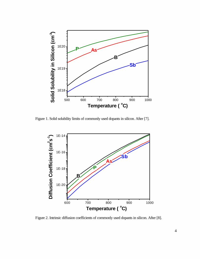
Table 1 lists the ionization energy values of various dopants in silicon, while Figure 1
compares their solubility limits [7]. Arsenic and phosphorous stand out as the best
choices for n-type doping. For deep-submicrometer devices that require abrupt doping
profiles, an additional requirement is a small diffusion rate of the dopant, which minimize
profile smearing during subsequent thermal processing steps. Figure 2 compares
diffusion coefficients of the same dopants in the typical IC processing temperature range
[8]. Compared to phosphorous, arsenic has a clear advantage of a much smaller diffusion
coefficient. For the above reasons, arsenic has become the best choice for heavy n-type
doping of silicon. It is important to study and understand its incorporation and activation
mechanism.
Dopant B As P Sb
Type acceptor donor donor donor
Ionization Energy (meV) 45 54 45 39
Table 1. Ionization energies of commonly used dopants in silicon. [6]
4
Figure 1. Solid solubility limits of commonly used dopants in silicon. After [7].
Figure 2. Intrinsic diffusion coefficients of commonly used dopants in silicon. After [8].
500 600 700 800 900 1000
1E18
1E19
1E20
Sb
AsP
BS
olid
Sol
ubili
ty in
Sili
con
(cm
-3)
Temperature ( oC)
600 700 800 900 1000
1E-20
1E-18
1E-16
1E-14
SbAs
P
B
Diff
usio
n C
oeff
icie
nt (c
m2 s-1
)
Temperature ( oC)

5
1.3 COMPARISON OF AVAILABLE ARSENIC INCORPORATION PROCESSES
1.3.1 ION IMPLANTATION
There are several ways of introducing dopant atoms into the Si lattice. Ion implantation is
the most widely used technology for this purpose because of its excellent controllability
and reproducibility. Dopants are accelerated to a certain energy and targeted to the silicon
substrate. They penetrate the surface, collide with host atoms, and eventually lose all their
energy and come to a stop in the lattice. Implantation distributes dopant atoms over a
range of distances from the surface. Atomic collisions disturb the crystalline structure of
silicon and create point defects and amorphous regions that require post-anneal to
activate the dopant and repair damage to the substrate. Dopant diffusion during this
anneal is significant due to implant-induced crystal defects. These pose limits on the
depth resolution. In the case of arsenic, the minimum junction depth achievable by
implantation was estimated to be about 20 nm, insufficient to meet the ITRS roadmap
requirement beyond year 2008 [1]. Additionally, implantation could not achieve abrupt
buried layers needed for modulation doping.
In conventional ion implantation followed by rapid thermal anneal (RTA), a dopant
profile is formed that is either Gaussian or exponential, neither of which is the optimum
rectangular box-shaped form. It has been proposed that laser thermal annealing (LTA) is
a method that has potential for avoiding some of the problems associated with RTA. The
approaches that have been recommended include melting the silicon crystal in the
presence of the dopant, or pre-amorphizing the silicon surface via implantation followed

6
by a dopant implant into the amorphous region, and then laser melting the amorphous
region [9][10]. Amorphous silicon has a melting temperature 300 ºC lower than
crystalline silicon. This large difference in melting temperature could provide an
opportunity for controlling junction depth by choosing the laser power to be sufficient to
melt the amorphous silicon, but insufficient for melting crystalline silicon. In this case,
the dopant will diffuse only through the melted amorphous region and will be electrically
activated during crystal regrowth. The process of melting the amorphous rather than
crystalline material overcomes some of the integration problems such as gate melting and
deformation that are generated by the laser power required to melt crystalline silicon.
Additional research is required to determine how well the LTA leaves the silicon defect-
free and how the process can be integrated into the process flow.
1.3.2 CHEMICAL VAPOR DEPOSITION (CVD) AND RELATED EPITAXY TECHNIQUES
In recent years, chemical vapor deposition (CVD) has undergone substantial development
for silicon-based epitaxy. Using epitaxy, the maximum doping concentration, thickness
and location of the doping profile can be chosen independently, providing a significant
advantage over ion implantation for applications that require such versatility.
1.3.2.1 CVD Background
Silicon epitaxy, in its simplest form, is performed at atmospheric pressure, employing
high-purity gaseous silicon sources, such as silane (SiH4), or one of a variety of silicon
halides, SiH4-xClx. The precursor, often highly diluted in an inert carrier gas, is passed
through a reactor chamber, where it is thermally decomposed to form a film upon a

7
silicon substrate. A refinement to silicon CVD enabled the addition of dopant species
during deposition, and the fabrication of precisely doped, uniform blanket epitaxial
layers. This contrasts with bulk silicon, which is limited by crystal pulling methods and
have an accuracy of wafer resistivity of roughly a factor of 2. Furthermore, CVD
epilayers also have the advantages of lower impurity and crystalline defect
concentrations. Consequently, bulk silicon wafers capped with CVD epilayers have
become an industry standard as starting material upon which devices are formed.
Besides providing a “substrate”, epitaxy also offers a powerful alternative to device
fabrication when it is used to directly deposit active layers in a device. This capability
creates tremendous new freedom for device design. For such processes, it is critical to
avoid autodoping, a phenomenon where existing doped regions in a substrate transfer
substantial amounts of dopant into the epitaxial layer being deposited, creating vertical
and horizontal distortions in the desired device geometry. Autodoping has been studied in
detail and found to have separate components caused by both solid-state migration of
dopant species from the substrate into the epilayer, and evaporation of dopant from the
substrate into the gas stream, which can subsequently be reincorporated in wafers
downstream in the gas flow [11][12]. Lower operating pressure and temperature were
adopted to reduce autodoping. The reduction of system operating pressure served to
eliminate a slowly flowing boundary layer of gas immediately above the substrate,
allowing more rapid transport of evaporated species away from the substrate, thus
reducing this component of autodoping. Additionally, the reduction of operating
temperatures reduces both dopant evaporation and solid-state diffusion. The resultant
8
process, referred to as low-pressure CVD (LPCVD), has become the growth method of
choice for conventional silicon epitaxy[13]. Further reduction in operating pressure leads
to UHVCVD[14], which utilizes turbo molecular pumps to achieve both low base
pressures in the UHV regime (hence the name), and relatively low operating pressures
typically in the militorr range or lower to achieve more accurate thickness control. The
much reduced operating pressure range and a cold-wall system also decrease gas-phase
reactions and enable the use of disilane (Si2H6), a more efficient Si precursor, to replace
silane, which requires higher growth temperatures.
Another related technique is gas-source molecular beam epitaxy (GSMBE), also known
as chemical beam epitaxy (CBE). It differs from UHVCVD by combining the beam
concept developed in MBE (see section 1.3.3 for more details) with the exclusive use of
chemical precursors. Instead of premixed source gases uniformly flowing through the
reactor chamber, individual gases can be injected toward the substrate from separate
injectors as molecular beams. The beam nature of GSMBE offers several advantages.
First, it eliminates the flow patterns present in CVD reactors, which can cause thickness
and composition non-uniformity. Secondly, it also minimizes any chemical reactions
between the gases before they impinge on the substrate surface. Such reactions can be
detrimental to the growth process. Finally, it reduces gas memory effects and allows, as
in MBE, excellent control of epilayer thickness and abruptness for heterostructure
growth.

9
1.3.2.2 Challenges to Arsenic Incorporation
A critical topic in Si epitaxy is dopant incorporation. When arsenic is used for n-type
doping, heavy doping levels and abrupt transitions are difficult to realize. This is a result
of both poor adherence and surface segregation of arsenic. CVD uses AsH3 as the arsenic
source, which has a narrow temperature window for useful deposition. At growth
temperatures lower than 600 ºC, the surface is largely terminated by hydrogen, which
greatly decreases the reactive sticking probability of AsH3. Above 700 ºC, arsenic
evaporation from the silicon surface becomes large and it is difficult to maintain an
adsorbed layer. Between 600 and 700 ºC, while it is possible to maintain arsenic
chemisorption on the surface, severe surface segregation is observed. Arsenic has one
more valence electron than Si does. Its presence on the Si surface terminates a dangling
bond and reduces surface energy [15]. Incorporated As atoms therefore tend to
segregate to the surface under equilibrium conditions, resulting in incorporated bulk
concentrations lower than those on the surface by several orders of magnitude. The
surface accumulation layer acts as a reservoir of arsenic for the growth. In the beginning
of doped growth, a sufficient amount of arsenic needs to accumulate on the surface
before equilibrium incorporation can be achieved. The incorporated arsenic concentration
therefore gradually ramps up to the maximum value as the equilibrium surface
accumulation layer is established. Similarly, after the AsH3 supply is interrupted at the
end of the doped growth, the surface accumulation layer continues to serve as a source
for doping subsequently grown material, until it is depleted by desorption and
incorporation. This significantly limits the maximum attainable doping level and

10
abruptness of the doping profile. Furthermore, CVD inherently suffers from gas memory
effects resulting from its relatively high operating pressures. After a certain source gas
supply is interrupted, it takes some time for related species to be completely purged from
the ambient and reactor chamber walls. This leads to further smearing of chemical
profiles.
Surface segregation of arsenic not only limits arsenic incorporation, but has other adverse
effects on the growth process. Near unity surface coverage by arsenic is needed in order
to increase the incorporated arsenic level to the 1018 cm-3 range. Surface arsenic
terminates dangling bonds and blocks further hydride adsorption, resulting in a
significant reduction in growth rate. It also retards surface diffusion and interferes with
the step-flow growth mode. As a result, epilayers with arsenic levels higher than 1018 cm-
3 often suffer from surface roughening and electrical degradation [16][17].
Due to the above difficulties with arsenic incorporation, many novel device structures
have only been demonstrated using p-type modulation doping with boron.
Complimentary structures are urgently needed to enhance performance in CMOS circuits.
1.3.3 MOLECULAR BEAM EPITAXY (MBE)
Molecular beam epitaxy (MBE) is a versatile epitaxy technique with the capacity for
monolayer-scale control. The capabilities of realizing well-controlled abrupt doping
profiles and alloy heterojunctions offer many opportunities to implement device
structures which have not been practical or realizable in the past. The development of Si
MBE technology is particularly important since there is an enormous Si technology base

11
already existing in industry, and any new advance in Si technology is extremely
important to the semiconductor industry as a whole.
Material sources are typically Knudsen effusion cells from which molecular beams are
generated by thermal evaporation or sublimation. The solid or liquid elemental source
material is held in an inert crucible typically made of pyrolytic boron-nitride and heated
by radiation. The vapor pressure of each species is controlled by setting the temperature
of the effusion cell and is monitored with a beam-flux ion gauge that can be inserted in
place of the substrate. Tantalum shutters in front of each cell can be opened and closed to
control the deposition of individual elements with monolayer accuracy.
The pressure in an idling MBE growth chamber is maintained in the UHV range,
typically 10-11 to 10-9 torr, by a combination of pumps, including ion pump, cryogenic
pump, turbo molecular pump, and liquid-nitrogen-filled cryo shroud. The UHV
environment allows deposition with extremely low impurity concentrations and enables
the use of in-situ surface analysis tools, such as reflective high energy electron diffraction
(RHEED) and Auger electron spectroscopy (AES). More importantly, it maintains source
fluxes in the molecular flow regime, so that individual molecules do not collide or react
with each other before reaching the substrate, and species that miss or desorb from the
substrate are pumped away immediately.
In the case of conventional silicon MBE, electron-beam evaporators (E-guns) are usually
used for producing silicon beams, since the vapor pressure of silicon is extremely low,
and conventional effusion cells cannot generate sufficient silicon vapor. It offers simple

12
growth control due to the unity sticking coefficient of elemental silicon, and a wide
temperature range for growth. However, E-guns have problems, such as poor growth rate
control, electronic shut-down due to electrical discharge in e-beam source, and generation
of surface defects due to charging of particles in the chamber. In the early work on gas-
source MBE, these problems were found to be easily eliminated by introducing gas
sources instead of E-guns.
Solid-source MBE work on n-type doping of silicon has focused on antimony because of
the ease of source control [18][19][20]. Similar to arsenic, antimony suffers from severe
surface segregation during growth at elevated temperatures. It was demonstrated that
antimony surface segregation can be effectively suppressed and very abrupt transitions
achieved in d-doped layers by using low substrate temperatures. Although active
concentrations higher than the equilibrium solid solubility can be achieved by this low-
temperature process, deactivation during subsequent thermal theatment is likely, and
compatibility with IC processes needs to be established. Arsenic and phosphorous, on the
other hand, have high equilibrium vapor pressures at relatively low temperatures, in the
100 – 200 ºC range, making precise flux control difficult when they are used as dopant
sources. Furthermore, arsenic vapor generated at such low temperatures is mainly
composed of As4, which has low sticking probability and tends to remain in the ambient
for a prolonged time period and cause memory effects. Arsenic-delta-doping was
demonstrated in (111) silicon epitaxy using a thermally evaporated As4 source, and Pb
was used as a surfactant [21]. However the background arsenic concentration was
relatively high, estimated to be in the 1019 cm-3 range, because of the arsenic memory

13
effect. Such a high doping level leads to significant conduction in the capping layer and
complicates electrical evaluation of the d-doped layer.
During the present work, a unique combination of solid and hydride gas sources
facilitates exploration of various growth techniques to carry out in-depth studies of
arsenic incorporation in silicon-based epitaxy. In particular, for the arsenic source, we
used As2 molecules produced by a valved cracking cell. As2 is more reactive than either
AsH3 or As4. To our knowledge this is the first attempt to dope silicon with such a
source.
1.4 ORGANIZATION
The aim of this dissertation is to report the fabrication and characterization of arsenic-
doped silicon-based (001) epitaxial layers. The focus is on silicon homoepitaxy with
limited discussion of SiGe heteroepitaxy on silicon. Chapter 2 discusses arsenic
incorporation and surface segregation during mixed gas- and solid-source MBE of silicon
and SiGe. A new segregation model is proposed to explain observed deviation from
existing segregation theory predictions. Effects of germanium concentration on arsenic
surface segregation in SiGe are also discussed.
Chapter 3 presents results on solid-source MBE of arsenic-doped silicon and SiGe. It is
shown that by using relatively low substrate temperatures, the segregation process
becomes kinetically limited, and extremely high concentrations of arsenic beyond
segregation and solubility limits can be achieved. Additional mechanisms that can limit

14
arsenic incorporation in this regime, as well as adverse effects arsenic has on the growth,
are also discussed.
Chapter 4 examines electrical properties of these heavily doped silicon materials. Carrier
concentrations and mobilities are studied in both as-grown and annealed materials and
compared with bulk values. Microstructure analysis results are discussed in an effort to
understand deactivation and carrier scattering mechanisms associated with heavy doping.
Discussion so far has been limited to relatively thick, uniformly doped epilayers. Chapter
5 investigates improvements to electrical properties over bulk limits by spatially
confining dopants in thin modulation-doped layers. It is shown that a spatial confinement
indeed provides enhancements both in electrical activation and carrier mobility. The
former is explained by reduction of atomic-scale clusters, and the latter by quantum-
mechanical effects.
Finally, Chapter 6 summarizes contributions made in this dissertation and makes
recommendations for future experimental and modeling work needed in the field.

15
CHAPTER 2: ARSENIC INCORPORATION DURING MIXED SOLID- AND GAS-
SOURCE GROWTH
This chapter discusses arsenic incorporation and surface segregation during mixed gas-
and solid-source MBE of silicon and SiGe.
2.1 EXPERIMENTAL PROCEDURE
Epilayers were deposited in a Varian Gen-II MBE system originally designed for III-V
compound growth, but modified during this work for Si-based growth with both solid and
gas sources. Sources used in this part of the experiments include Si2H6 gas, Ge generated
by a standard effusion cell, and As2 generated by a valved cracker cell. Additional
sources available on the system include hot-filament sources for silicon and titanium, as
well as standard effusion cells for aluminum, gallium, and boron.
To maintain UHV and minimize contamination during wafer loading, the system has a
separate loading chamber, which is connected to the growth chamber through a transition
tube. The vacuum in the growth chamber is maintained by the combination of a 2000
l/minute turbo molecular and mechanical pumping system, a 400 l/minute ion pump, and
a liquid nitrogen cryo shroud that surrounds the growth area. The growth chamber
pressure is typically in the 10-11 torr range when idling, in the 10-9 torr range during solid-
source growth, and in the 10-7 torr range during growth with Si2H6. The cryo shroud is
warmed to room temperature after each growth to release disilane gas trapped on its cold
16
surface during the growth. The gas is evacuated by the turbo molecular pump into an
enclosed manifold, where it is diluted with large amounts of nitrogen and bubbled
through a water scrubber before being released to air.
Nominally (100)-oriented p-type Si wafers 3” in diameter and 1-10 ohm-cm in resistivity
were used as substrates. Wafers were cleaned with a modified chemical etching process
consisting of 10 minutes in a H2SO4:H2O2 (4:1) bath maintained at 90°C, 30 seconds in a
H2O:HF (50:1) bath at room temperature, and 10 minutes in a H2O:H2O2:HCl (5:1:1) bath
maintained at 70°C, with 6 cycles of dump DI water rinse following each step. This
cleaning procedure leaves a thin and volatile oxide protection layer on the surface. After
wet cleaning, wafers are spun-dry and immediately loaded. The loading chamber is
pumped to high vacuum and wafers are pre-baked at 200 °C for 1 hour in the loading
chamber to desorb water. Baked wafers are then stored in the transition tube maintained
at 5 × 10⁻¹⁰ torr. Immediately before growth, the protective oxide is desorbed in-situ in
the growth chamber at 850 °C to yield a clean, well-ordered surface characterized by
double domain (1 × 2) + (2 × 1) surface reconstruction, as observed by RHEED. Using
this cleaning procedure, no residual oxide can be observed at the substrate-epilayer
interface by SIMS, which has a detection limit of roughly 1018 cm-3 for oxygen.
During growth, the substrate is heated radiatively and the temperature is monitored with a
thermocouple located in close proximity to the back side of the wafer. The thermocouple
temperature reading is calibrated with a two-channel SVT pyrometer, and verified by
observing the Si-Al eutectic at 577°C. A substrate temperature of 655 °C is used for all

17
experiments discussed in this chapter. Background impurities are monitored by an SRS
residual gas analyzer equipped with an electron multiplier, while the wafer surface is
monitored by reflective high-energy electron diffraction (RHEED) using a Creekside
electron gun operating at 11 KeV.
The disilane gas used is of 99.999% purity by Votaix. The gas is injected into the
chamber toward the substrate through a Riber gas injector with a diffuser attachment to
enhance uniformity. The gas flow rate is controlled with a digital mass-flow controller. A
gas flow rate of 2.5 sccm is used throughout the following experiments, which
corresponds to a beam flux pressure of 8 × 10⁻⁶ torr, or a flux of 2 × 1015 cm-2s-1. Typical
germanium cell temperatures range from 1000 to 1120 ºC, which yields growth rates
ranging from 0.005 to 0.12 nm/minute.
Use of a solid arsenic source eliminates the lower limit to substrate temperature imposed
by thermal decomposition of AsH3 and allows more room in optimizing growth
parameters to improve arsenic incorporation. Arsenic has very high vapor pressures and
requires relatively low temperatures, in the range of 100 to 400 ºC, to generate typical
MBE fluxes. Vapor generated at these low temperatures is mainly composed of As4
molecules, which do not stick well to the substrate. At higher temperatures, As4 can be
thermally cracked into more reactive As2 molecules, which are more efficient precursors
for deposition. The arsenic cracker cell was developed to supply As2 in a flux range
useful for MBE. It operates in two zones. The sublimation zone generates As4 vapor by
heating solid arsenic to relatively low temperatures, up to 450 ºC. The final beam flux is
18
largely controlled by the temperature in this zone. The vapor is then injected toward the
substrate through a cracking zone at the tip of the cell, which is heated to a higher
temperature, typically in the range of 700 to 800 ºC, to crack As4 into As2 molecules. A
stem valve at the tip of the cell further adjusts the flux to desired values. The cracker cell
was originally developed for III-V semiconductor deposition. To our knowledge this is
the first attempt to use it as a dopant source for group IV deposition. In order to generate
smaller source fluxes suitable for doping, the sublimation zone is maintained at 120 ºC,
while the cracking zone temperature is varied between 600 and 700 ºC to control the
percentage of active As2 molecules in the source vapor. It is estimated that the fractions
of As2 in the vapor cracked at these temperatures are roughly 60% and 85%
respectively[22]. The total flux is further adjusted by the stem valve to be in the range of
2 × 10⁻⁹ – 1.6 × 10⁻⁸ Torr.
Epilayer topography was characterized by contact-mode atomic-force microscopy (AFM)
using a Digital Instruments Multi-mode Scanning Probe Microscope. Arsenic,
germanium, and background impurity concentration profiles were measured by secondary
ion mass spectroscopy (SIMS) using 500 or 1000 eV Cs+ primary ion beams. Impurity
concentrations are calibrated by simultaneously measuring standard samples with known
profiles of the measured elements, and profile depths are calibrated by measuring the
depth of the sputtered raster with a profilometer. Arsenic profile depth resolutions are
estimated to be roughly 3 and 2 nm/dec in the leading and trailing edges respectively.
High-resolution transmission electron microscopy (HRTEM) was performed using a
Philips CM20 microscope operating at 200 kV with a field-emission tip. Cross-section

19
samples were prepared by manually polishing to ~10 micrometers, followed by ion
milling on a Precision Ion Processing System. Ar ion beams with an energy of 3.5 KeV
and incident angle of 6º were used. High-resolution imaging was performed along the
[110] zone axis perpendicular to the wafer surface. Bright- and dark-field imaging were
performed under two-beam conditions using the (004) diffracted beam parallel to the film
growth direction.
2.2 RESULTS
2.2.1 ARSENIC INCORPORATION IN SILICON
Similar to previous reports on CVD and GSMBE results [16][23], addition of arsenic
significantly reduced the silicon growth rate from disilane. Figure 3 plots silicon growth
rate as a function of incorporated arsenic concentration in a series of samples grown with
the same substrate temperature and disilane flux, but different arsenic fluxes. While there
is a modest change in incorporated arsenic concentration from mid-1017 cm-3 to low 1018
cm-3 range, the silicon growth rate was reduced by more than an order of magnitude for
the more heavily doped materials. Efforts to achieve higher doping concentrations by
increasing the arsenic flux or by using lower substrate temperatures were unsuccessful
because of the prohibitively small growth rates.
20
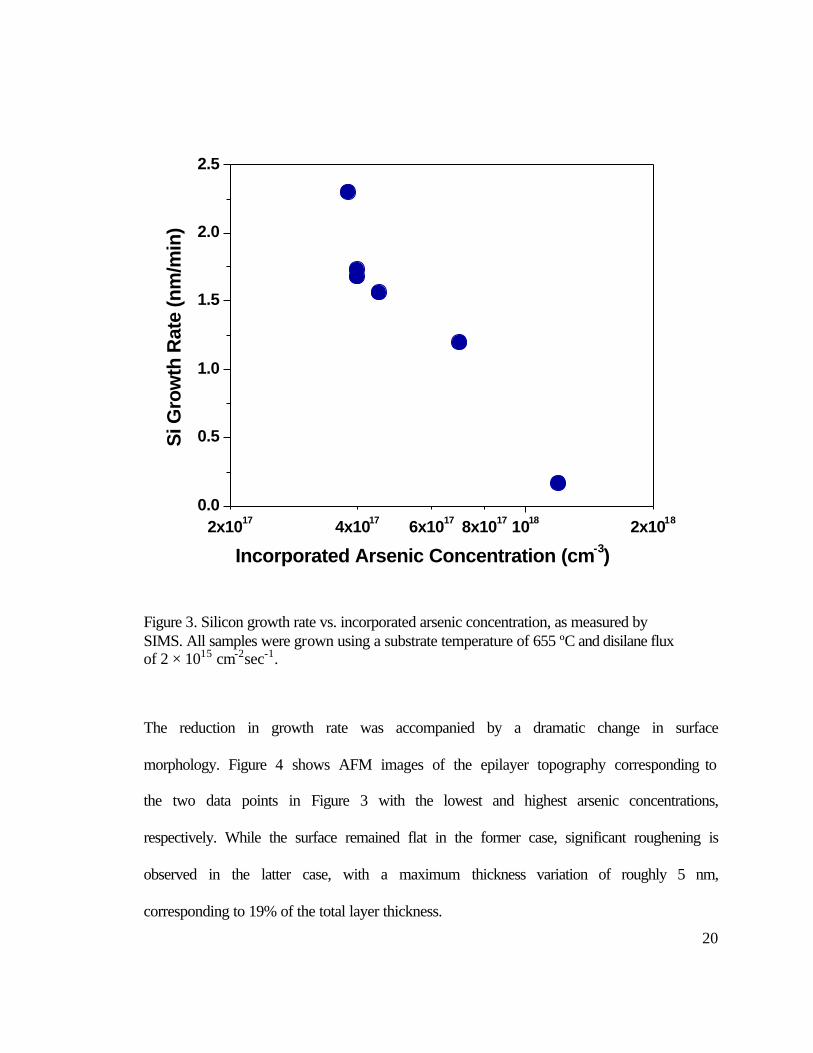
Figure 3. Silicon growth rate vs. incorporated arsenic concentration, as measured by SIMS. All samples were grown using a substrate temperature of 655 ºC and disilane flux of 2 × 1015 cm-2sec-1.
The reduction in growth rate was accompanied by a dramatic change in surface
morphology. Figure 4 shows AFM images of the epilayer topography corresponding to
the two data points in Figure 3 with the lowest and highest arsenic concentrations,
respectively. While the surface remained flat in the former case, significant roughening is
observed in the latter case, with a maximum thickness variation of roughly 5 nm,
corresponding to 19% of the total layer thickness.
2x10¹⁷ 4x10¹⁷ 6x10¹⁷ 8x10¹⁷ 1018 2x10180.0
0.5
1.0
1.5
2.0
2.5S
i Gro
wth
Rat
e (n
m/m
in)
Incorporated Arsenic Concentration (cm-3)

21
Figure 4. AFM images of the epilayer topography corresponding to the two data points in Figure 3 with (a) the lowest and (b) the highest arsenic concentrations, respectively.
Figure 5 shows bright-field, dark-field, and high-resolution cross-section TEM images of
the sample shown in Figure 4 (b). A curvature on the epilayer surface is apparent, which
corresponds to the roughness shown in Figure 4 (b). An important observation from these
images is the absence of extended defects, such as dislocations or stacking faults, in
association with the roughness. The morphology appears to be related to surface growth
mechanisms and not to the development of any specific crystallographic defect visible in
TEM.
(a) (b)

22
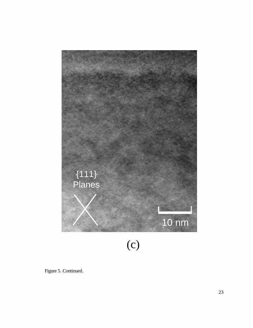
Figure 5. (a) Bright-field, (b) dark-field, and (c) high resolution (see next page) cross-section TEM images of sample shown in Figure 4(b). Under the two-beam diffraction conditions used for (a) and (b), the images are sensitive to disorder caused by extended defects, such as dislocations, precipitates, and stacking faults.
Epilayer
Substrate
26nm
(a)
(b)
23
Figure 5. Continued.
{111}Planes
10 nm
(c)
24
2.2.2 ARSENIC INCORPORATION IN SiGe
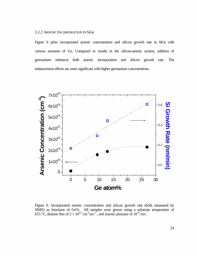
Figure 6 plots incorporated arsenic concentration and silicon growth rate in SiGe with
various amounts of Ge. Compared to results in the silicon-arsenic system, addition of
germanium enhances both arsenic incorporation and silicon growth rate. The
enhancement effects are more significant with higher germanium concentrations.
Figure 6. Incorporated arsenic concentration and silicon growth rate (both measured by SIMS) as functions of Ge%. All samples were grown using a substrate temperature of 655 ºC, disilane flux of 2 × 1015 cm-2sec-1, and arsenic pressure of 10-8 torr.
0 5 10 15 20 25 30
0
1x10¹⁹
2x10¹⁹
3x10¹⁹
4x10¹⁹
5x10¹⁹
6x10¹⁹
7x10¹⁹
Ge atom%
Ars
enic
Con
cent
ratio
n (c
m-3)
0.0
0.2
0.4
0.6
Si G
rowth R
ate (nm/m
in)

25
2.3 DISCUSSION
2.3.1 GROWTH MECHANISM
The pyrolysis of Si2H6 during homoepitaxy of Si is known to occur through dissociative
chemisorption followed by sequential loss of hydrogen [24]. The reduction of SiH3 and
SiH2 to the monohydride phase is considered to be fast. The Si2H6 dissociative adsorption
and the eventual hydrogen desorption from the monohydride control the overall growth
rate. H atoms on the surface terminate dangling bonds, prohibiting further disilane
adsorption on these sites. Disilane adsorption rate, and therefore the silicon growth rate,
follow a second order relationship with respect to dangling bond density. From the above
discussion, one can anticipate two distinctive growth modes resulting from competition
between the dissociative adsorption of Si2H6 and the hydrogen desorption from the
monohydride. If the hydrogen desorption rate is high enough compared with the Si2H6
adsorption rate, the growth is determined by the Si2H6 supply, and the growth rate
becomes proportional to the Si2H6 flux. If the growth temperature is relatively low and
the hydrogen desorption rate is not high enough, the growth is limited solely by hydrogen
desorption. The latter growth mode is called reaction-limited growth, while the former is
called supply-limited growth.
Under the conditions used in these experiments, undoped growth occurs in the strongly
supply-limited regime [25], and surface H coverage is estimated to be less than 5%.
Surface H has been observed to change the apparent surface segregation energy of
arsenic by blocking surface sites needed for segregation [26]. Its presence also changes
26
the adsorption behavior of arsenic and Si2H6, adding second-order effects to arsenic
incorporation. It is therefore important, in order to quantitatively study the true atomic
segregation of arsenic, that surface H coverage remains low during growth. During the
following discussions on arsenic surface segregation, we will neglect the effects of
surface H. A simple calculation using the model developed in reference [26] shows that,
even with 5% of the surface occupied by H, the error incurred in our model by making
this simplification is still insignificant and less than the fluctuations in the measured data.
2.3.2 ARSENIC SURFACE SEGREGATION
In the following, we attempt to interpret the above results of arsenic incorporation in
terms of a two-site exchange surface segregation model [27][19][28]. Figure 7 shows a
schematic diagram of a silicon (001) surface with some atomic sites occupied by arsenic.
Each silicon atom has four valence electrons. A clean silicon (001) surface is
characterized with alternating (2 x 1) and (1 x 2) reconstruction domains. Each silicon
atom bonds with two atoms in the underlying layer and one other atom on the surface. In
this configuration each silicon atom has a lone valence electron, or dangling bond,
making the surface very reactive. On the other hand, arsenic atoms on the silicon (001)
surface have only three valence electrons available for bonding and are found to form
symmetric dimers [29], with each arsenic atom bonding with two silicon atoms in the
underlying atomic layer and one other arsenic atom in the surface layer. Surface arsenic
atoms in this configuration are fully coordinated without dangling bonds, and are
expected to reduce surface energy significantly.

27
Figure 7. Schematic diagram of surface segregation on silicon (001) surface.
Energy
Location of As
Segregation Energy
SiAs
surface bulkimpinging flux
28
Immediately following deposition of a monolayer of silicon, arsenic atoms are buried into
subsurface sites, while surface sites are occupied by silicon atoms with dangling bonds. It
is energetically favorable for the arsenic atoms to migrate back to the surface. A
schematic potential energy diagram, also shown in Figure 7, can be used to describe this
exchange process. Assuming the subsurface state is energetically above the surface state
by the amount ?Gs, and the activation barrier between the two states is ?G+, the rate
equation to describe arsenic concentration in the subsurface layer can be written as
)()1()1( bsb
ss
bb nn
aNn
nKNn
nKt
n−+−+−−=
∂∂
−+β
Equation 1
where ns and nb represent arsenic concentrations in the surface and subsurface layers
respectively, N is the atomic density of bulk silicon (5 × 1022 cm-3), and K+ and K- are
thermally activated transition rates that can be represented as follows:
)exp(kTG
K ++
∆−= ν Equation 2
)exp()exp(kTG
KkT
GGK ss ∆
−=∆+∆
−= ++
− ν Equation 3
The “successful attempt” frequency ? is generally taken to be the same as the Debye
frequency, which has a typical value of 1013 sec-1. The third term in Equation 1 represents
a kinetic limit to segregation imposed by the burying process from continued deposition
of new material, where ß is the growth rate and a the atomic layer height. In the limit of
high growth temperatures or small growth rates, such as those used in the current work,
this term becomes small compared to the other terms and can be neglected [19][30][26].
29
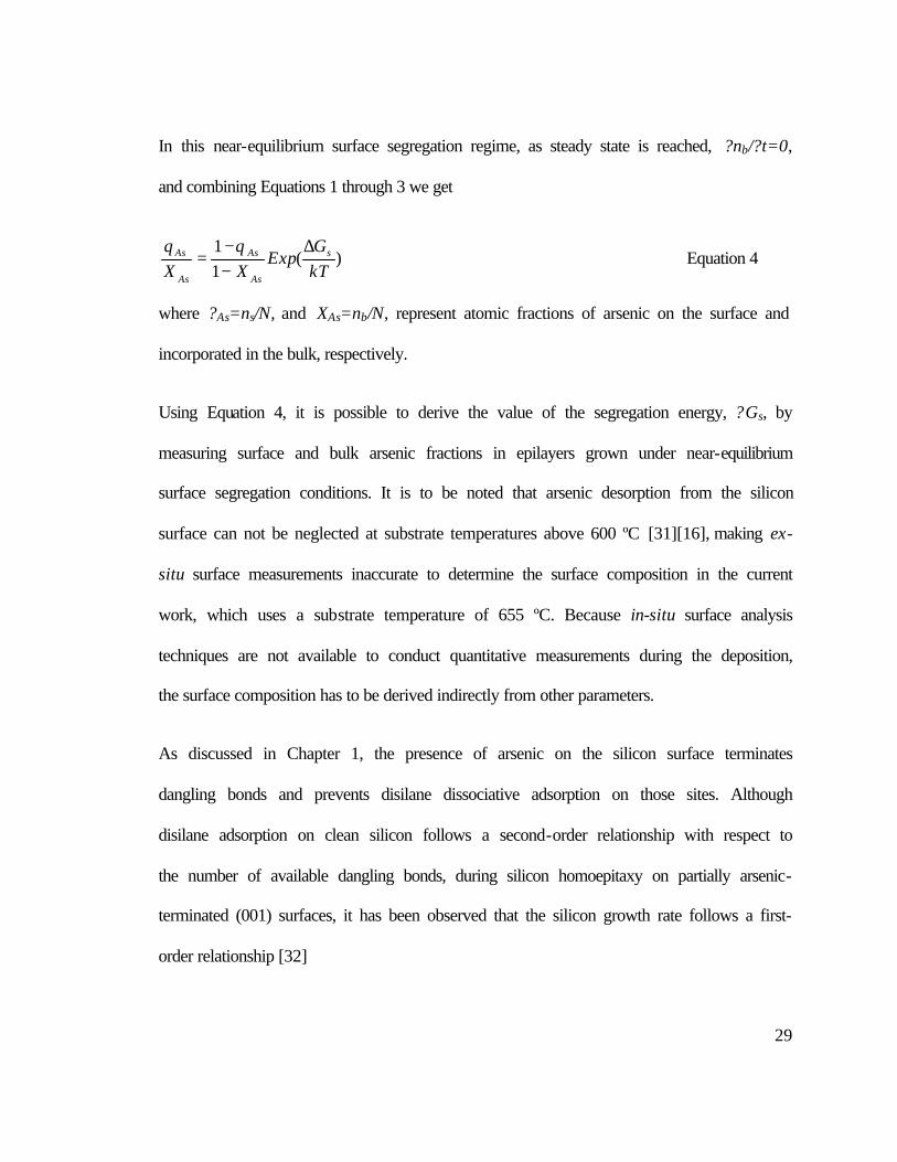
In this near-equilibrium surface segregation regime, as steady state is reached, ?nb/?t=0,
and combining Equations 1 through 3 we get
)(11
kTG
ExpXX
s
As
As
As
As ∆−−
=θθ
Equation 4
where ?As=ns/N, and XAs=nb/N, represent atomic fractions of arsenic on the surface and
incorporated in the bulk, respectively.
Using Equation 4, it is possible to derive the value of the segregation energy, ?Gs, by
measuring surface and bulk arsenic fractions in epilayers grown under near-equilibrium
surface segregation conditions. It is to be noted that arsenic desorption from the silicon
surface can not be neglected at substrate temperatures above 600 ºC [31][16], making ex-
situ surface measurements inaccurate to determine the surface composition in the current
work, which uses a substrate temperature of 655 ºC. Because in-situ surface analysis
techniques are not available to conduct quantitative measurements during the deposition,
the surface composition has to be derived indirectly from other parameters.
As discussed in Chapter 1, the presence of arsenic on the silicon surface terminates
dangling bonds and prevents disilane dissociative adsorption on those sites. Although
disilane adsorption on clean silicon follows a second-order relationship with respect to
the number of available dangling bonds, during silicon homoepitaxy on partially arsenic-
terminated (001) surfaces, it has been observed that the silicon growth rate follows a first-
order relationship [32]

30
)( As0 1RR θ−×= Equation 5
where R is the silicon growth rate on partially arsenic-terminated silicon surfaces, R0 is
the silicon growth rate on clean surfaces under otherwise identical conditions, and θAs is
the fraction of surface sites occupied by arsenic. This first-order relationship was
attributed to the strong tendency of surface arsenic to dimerize, which correlates the
number of missing neighboring dangling bond pairs with the fraction of surface sites
occupied by arsenic dimers. The above observation enables the calculation of the arsenic
surface fraction by comparing the silicon growth rate in these samples with that on a
clean substrate.
Figure 8 replots the data points in Figure 3 by converting growth rates into arsenic
surface fractions using Equation 5. It shows that the improvement in arsenic
incorporation under these growth conditions is very limited given the wide range of
arsenic surface fractions. Equation 4 is then used to calculate the segregation energy, with
results plotted as a function of arsenic surface fraction in Figure 9. It is shown that, the
segregation energy is not a constant, but varies with surface arsenic fraction. Linear
extrapolation of the data to zero and unity surface arsenic fractions gives segregation
energy values of 0.8 eV and 1.075 eV, respectively. The former value is consistent with
the 0.8 ± 0.05 eV given in reference [26], which is also established for small surface
arsenic fractions in the range of 3 to 8%.

31
Figure 8. Incorporated arsenic concentration as a function of surface arsenic fraction, calculated from data in Figure 3 using Equation 5.
The configuration of arsenic ad-atoms on the silicon (001) surface has been extensively
studied [15][33][29]. It is generally recognized that arsenic atoms have a strong tendency
to form symmetric dimers with no dangling bond. Furthermore, through both first-
principle calculations[15] and experimental observations [33], it was shown that arsenic
dimers on the surface attract each other and favor 2-dimensional islanding. In this
configuration, surface segregation of incorporated arsenic is energetically favored, with a
0.0 0.2 0.4 0.6 0.8 1.02E17
3E17
4E17
5E17
6E177E178E179E171E18
2E18
CA
s: A
rsen
ic B
ulk
Con
cent
ratio
n (c
m-3)
θAs
: Arsenic Surface Coverage
32
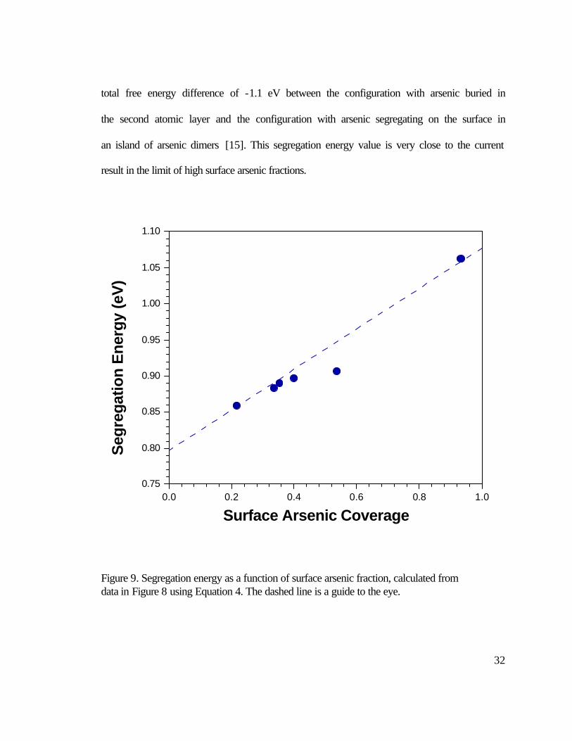
total free energy difference of -1.1 eV between the configuration with arsenic buried in
the second atomic layer and the configuration with arsenic segregating on the surface in
an island of arsenic dimers [15]. This segregation energy value is very close to the current
result in the limit of high surface arsenic fractions.
Figure 9. Segregation energy as a function of surface arsenic fraction, calculated from data in Figure 8 using Equation 4. The dashed line is a guide to the eye.
0.0 0.2 0.4 0.6 0.8 1.00.75
0.80
0.85
0.90
0.95
1.00
1.05
1.10
Seg
rega
tion
Ene
rgy
(eV
)
Surface Arsenic Coverage

33
Under growth conditions used in the current work, the surface is at an elevated
temperature with significant arsenic desorption. The surface arsenic population is
maintained by a dynamic balance between the incoming and the desorbing fluxes. It is
reasonable to speculate that, in the limit of low arsenic surface coverage, islanding is
suppressed kinetically, and a significant fraction of arsenic exists as isolated dimer pairs.
These isolated dimers have a somewhat higher energy compared to those forming islands,
corresponding to a smaller segregation energy. As arsenic coverage approaches unity,
island density increases and most arsenic atoms now reside in islands, resulting in an
increase in the average segregation energy. We therefore propose, based on the above
discussion, that the surface-composition-dependence of segregation energy observed in
the current experiments reflects a change in the configuration of surface arsenic dimers,
from mostly isolated dimers in the limit of low arsenic fractions, to mostly islands in the
limit of high arsenic fractions.
The above model is also consistent with the observed surface roughening associated with
high arsenic fractions, as shown in Figure 4. Because arsenic inhibits disilane dissociative
adsorption, it is reasonably speculated that growth of silicon on top of arsenic islands can
only occur through surface diffusion. However, as will be discussed in Chapter 3, high
surface fractions of arsenic also appear to retard surface diffusion, therefore the growth
rate in areas covered by large arsenic islands could be much lower than in those areas
covered by silicon, leading to variations in the epilayer thickness. Speculating further,
arsenic evaporation, deposition and surface migration during the growth can lead to

34
continuous disintegration of existing islands and nucleation of new ones. This would
explain why the indentations eventually fill in and only persist as slight depressions.
The enhancement effects of SiGe on arsenic incorporation can be explained by
competitive surface segregation. Germanium is a larger atom compared to silicon and
tends to surface segregate as well [34]. When both Ge and As are present, they compete
for surface sites. The number of available surface sites for arsenic segregation is therefore
reduced and its segregation is suppressed.
It is well know that germanium has an effect on the silicon surface which acts to enhance
the growth rate during GSMBE using hydride sources [35]. Presumably, the presence of
germanium on the surface enhances hydrogen desorption from germanium atoms and
increases the dangling bond density. This mechanism does not apply to the current
experiments, however, since surface hydrogen density is very low and does not limit the
growth rate. In fact, an enhancement in silicon growth rate was not observed in undoped
SiGe compared to that in undoped Si. The enhanced silicon growth rate in arsenic-doped
SiGe compared to arsenic-doped silicon reflects an increase in dangling bond density.
The steady-state surface arsenic fraction is maintained by a balance of three fluxes: the
incoming source flux, desorption, and incorporation into the epilayer. While the incoming
flux remains constant, incorporation is enhanced in SiGe. The desorption rate from
germanium is also enhanced, because the As-Ge bonding energy is smaller than that for
As-Si [36]. The net effect is a reduction of surface arsenic fraction, which leads to an
increase in dangling bond density and hence an increase in the silicon growth rate from

35
disilane. It should be noted that, despite this reduction in surface density, arsenic
incorporation is still greatly enhanced in SiGe because of the strong suppression of
surface segregation.
SiGe has great potential for device applications, such as strained-channel MOSFETs and
HBTs. The ability to dope SiGe in-situ is very important for such applications. However,
relying on the addition of germanium to silicon epitaxy to achieve heavy doping also
imposes other limitations, such as band-gap modification and strain. Development of
processes that can decouple arsenic incorporation from the SiGe composition is still
desirable.
Surface segregation is a thermally activated process and in principle can be kinetically
suppressed by using lower substrate temperatures or high growth rates. Under these
conditions, the segregation rate can be slow compared to the growth rate, and it is
possible to bury arsenic into the bulk before it has a chance to segregate back to the
surface. Once an arsenic atom is buried by a few monolayers of material, the energy
barrier for it to migrate back to the surface will be much higher and equal to the bulk
diffusion energy barrier, which requires higher temperatures to overcome. During the
above experiments, it has been shown that growth from disilane in the MBE mode
dictates the use of relatively high substrate temperatures to generate realistic growth
rates, particularly when arsenic is present. Such high temperatures combined with the
relatively small growth rates do not provide sufficient kinetic suppression. Furthermore,
because silicon growth on arsenic-terminated areas is retarded, kinetic suppression would
36
likely be ineffective, even if lower temperatures and higher growth rates can be
combined, for example by using much higher gas fluxes. A possible solution to this
problem is to replace disilane with a highly reactive silicon source that does not require
elevated temperatures or dangling bonds to incorporate.

37
CHAPTER 3: ARSENIC INCORPORATION DURING LOW-TEMPERATURE
SOLID-SOURCE GROWTH
This chapter presents results on solid-source MBE of arsenic-doped silicon and SiGe
using elemental sources for both silicon and germanium. The elemental silicon source has
unity sticking coefficient and does not require dangling bonds or high temperatures for
efficient adsorption. It is shown that, by combining elemental sources with relatively low
substrate temperatures, the segregation process becomes kinetically limited, and
extremely high concentrations of arsenic, well beyond surface segregation and solubility
limits, can be achieved. Additional mechanisms that may limit arsenic incorporation in
this regime are discussed. Adverse aspects of low-temperature epitaxy and effects of
arsenic are also investigated.
3.1 EXPERIMENTAL PROCEDURE
The growth setup used in this part of the experiments is identical to that described in
section 2.1, except that a solid silicon source was used for Si growth instead of disilane
gas. Elemental silicon vapor is generated by directly heating a high-purity silicon
filament with DC current. The temperature of the filament is estimated to be near 1000 ºC
by observing a thermocouple located behind the filament. Growth rates range from 3 to 8
nm/hour. Substrate temperatures during growth range from 300 to 545 °C. After
deposition, some samples were annealed in-situ at various temperatures. A temperature
ramp rate of 30 °C/minute is used.

38
Using a solid silicon source decouples the growth rate from arsenic coverage, so that
arsenic coverage can no longer be derived from growth rate. However, substrate
temperatures below 600 °C enable the use of ex-situ surface characterization tools to
directly measure the surface composition. Surface arsenic coverage was measured by
angle-resolved X-ray photoelectron spectroscopy (ARXPS) using Al (Ka) radiation
(1486 eV) as a probe. In XPS, soft X-rays illuminate a region of the sample being
analyzed, and photoelectrons emanating from it are energy analyzed. From the energy
spectrum, the elements present and their chemical state can be determined. Because only
electrons emitted by atoms near the surface of the sample can escape without losing
energy, the technique is very surface-sensitive. The electron escape depth ranges from
0.5-10 nm, depending on the electron energy, but is not a strong function of the material
composition. It is possible, by collecting photoelectrons at two different angles from the
sample surface, to extract information about the distribution of sample constituents with
depth. This is particularly useful in the current work because surface contaminants such
as water and organics can mask the arsenic signal. The detailed ARXPS procedure is
described in reference [37]. Elements detected on epilayer surfaces include Si, As, C and
O. Table 2 lists specific energy levels analyzed during the measurements, as well as
sensitivity and escape depth values used for the calculation.

39
Element Si As C O
Electron Energy Level 2s 3d 1s 1s
Sensitivity Factor[38] 1.03 2.07 1 2.49
Escape Depth (nm) [39] 0.62 0.55 0.87 1.2
Table 2. List of ARXPS parameters.
Arsenic and background impurity profiles were measured by SIMS. Epilayer topography
was characterized by RHEED and contact-mode AFM, as described in section 2.1.
3.2 RESULTS AND DISCUSSION
3.2.1 ARSENIC INCORPORATION IN SILICON
Figure 10 plots arsenic surface segregation relationships during low-temperature solid-
source MBE in the temperature range of 300 to 545 °C. Also plotted in Figure 10 are
equilibrium segregation curves, calculated from Equation 4 using the segregation energy
values derived in Chapter 2. The experimental results strongly deviate from the
equilibrium curves, with larger deviations at lower temperatures, indicating strong kinetic
suppression of segregation in this temperature range. As a result, extremely high arsenic
concentrations can be incorporated with relatively low surface fractions.
40
Figure 10. Incorporated arsenic concentration vs. surface arsenic fraction during low-temperature solid-source MBE (data points) in comparison with equilibrium surface segregation relations at corresponding temperatures (solid curves) calculated using segregation energy values derived in Chapter 2.
The equilibrium arsenic solubility limit at these temperatures is estimated to be in the
low 1019 cm-3 range [40]. Incorporated concentrations are up to two orders of magnitude
higher than this limit, consistent with the metastable nature of the growth.
Kinetic processes depend strongly on growth rates, as can be seen from Equation 1.
The Si growth rates used in these experiments are relatively small. Further kinetic
0.0 0.2 0.4 0.6 0.8 1.0
1E14
1E15
1E16
1E17
1E18
1E19
1E20
1E21 300 oC 460 oC 480 oC 525 oC 545 oC
300 °C
460 °C480 °C
545 °C 525 °C
CA
s: A
s B
ulk
Con
cent
ratio
n (c
m-3)
θAs
: Surface Coverage

41
suppression and better incorporation are possible with higher growth rates achievable
with an electron-beam-heated Si source. However, it should be pointed out that, as
surface segregation is suppressed and incorporated concentrations become significant,
further arsenic incorporation may be limited by other mechanisms. For example, when
neighboring arsenic atoms are only separated by a few silicon atoms, the Coulomb field
will no longer be completely screened, and ionized arsenic atoms will repel each other
through this field [41]. It has been proposed that such Coulombic repulsion may limit
dopant incorporation at high concentrations. Arsenic atoms also create local strain fields
(see Chapter 4). Such fields are a source of repulsive interaction similar to Coulomb
fields. Furthermore, during growth, an internal field is established near the surface as the
result of surface Fermi level pinning. The electrostatic dipole interaction between carriers
localized in surface states and their parent donors causes the donor to migrate along with
the surface as well [42]. During this work, an effort to model measured results with
Equation 1 did indicate an apparent enhancement of surface segregation at higher
concentrations, which may be related to the mechanisms discussed above.
3.2.2 ARSENIC INCORPORATION IN SiGe
Figure 11 compares incorporated arsenic concentrations in Si and SiGe during low-
temperature MBE. Contrary to the case in the strong surface segregation limit, where
germanium enhances arsenic incorporation by suppressing segregation, here the addition
of germanium appears to reduce arsenic incorporation. Several mechanisms may
contribute to this effect: as discussed in Chapter 2, germanium enhances arsenic

42
desorption from the surface, resulting in significant desorption at temperatures above 400
ºC[36], which in turn reduces its surface density when the source flux is maintained
constant. Also, the solubility limit of arsenic in germanium is lower than that in silicon
[43][44], which may suppress arsenic incorporation in SiGe even under kinetic limits.
Finally, germanium creates local compressive strain fields, which may repel incorporated
arsenic atoms toward the surface as well. A closer look into this material system is
needed to separate these effects, which is beyond the scope of this work.
Figure 11. Incorporated arsenic concentration in Si and SiGe as a function of atomic Ge fraction. All samples were grown using a substrate temperature of 480 ºC and arsenic pressure of 7 × 10⁻⁹ torr.
0 2 4 6 8 10 12 14 16 182E20
3E20
4E20
5E20
6E20
7E20
8E209E20
Ars
enic
Con
cent
ratio
n (c
m-3)
Ge%
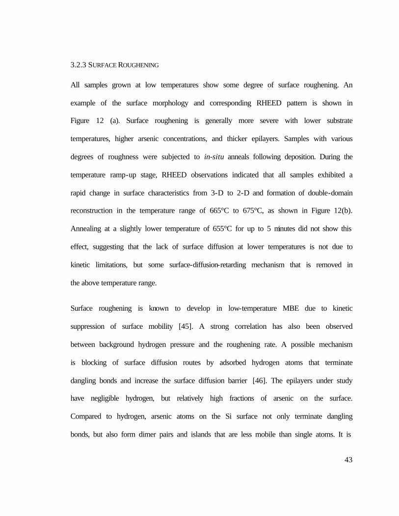
43
3.2.3 SURFACE ROUGHENING
All samples grown at low temperatures show some degree of surface roughening. An
example of the surface morphology and corresponding RHEED pattern is shown in
Figure 12 (a). Surface roughening is generally more severe with lower substrate
temperatures, higher arsenic concentrations, and thicker epilayers. Samples with various
degrees of roughness were subjected to in-situ anneals following deposition. During the
temperature ramp-up stage, RHEED observations indicated that all samples exhibited a
rapid change in surface characteristics from 3-D to 2-D and formation of double-domain
reconstruction in the temperature range of 665°C to 675°C, as shown in Figure 12(b).
Annealing at a slightly lower temperature of 655°C for up to 5 minutes did not show this
effect, suggesting that the lack of surface diffusion at lower temperatures is not due to
kinetic limitations, but some surface-diffusion-retarding mechanism that is removed in
the above temperature range.
Surface roughening is known to develop in low-temperature MBE due to kinetic
suppression of surface mobility [45]. A strong correlation has also been observed
between background hydrogen pressure and the roughening rate. A possible mechanism
is blocking of surface diffusion routes by adsorbed hydrogen atoms that terminate
dangling bonds and increase the surface diffusion barrier [46]. The epilayers under study
have negligible hydrogen, but relatively high fractions of arsenic on the surface.
Compared to hydrogen, arsenic atoms on the Si surface not only terminate dangling
bonds, but also form dimer pairs and islands that are less mobile than single atoms. It is
44
speculated that arsenic plays a similar role to that of hydrogen in promoting surface
roughening in these materials. Arsenic starts to desorb from (100) Si surfaces in the
temperature range of 650-700°C [16][31], consistent with the observed surface diffusion
enhancement near these temperatures.
Figure 12. Epilayer surface morphology and corresponding RHEED patterns : (a) after 18 nm of growth at 480 °C; and (b) after growth at 480°C and in-situ annealing at 675 °C. AFM images are 1 µm × 1 µm in size.
45
3.2.4 CRITICAL EPITAXY THICKNESS
During low-temperature MBE, a critical epitaxy thickness exists beyond which
crystalline growth is followed by a transition to amorphous deposition. This critical
epitaxy thickness has been studied by a variety of groups for undoped silicon
homoepitaxy. It has been found to be a strong function of the growth temperature, and
also related to the growth rate and presence of background hydrogen in the vacuum [46].
Although the exact mechanism is not fully understood, several models have been
proposed that relate the critical epitaxy thickness to accumulation of point-defects in the
material [19], surface roughening [46] or a super-saturation of the growing layer with
atomic hydrogen, which is mainly generated by the E-beam evaporator used for silicon
deposition [47][48]. Hydrogen has been linked to interruption of the step-flow growth
mode and promotion of roughening and defect formation [46].
Epilayers grown in this work all have thicknesses below the reported values of critical
epitaxy thickness at corresponding temperatures, and those grown above 400°C indeed
remained single-crystalline, as observed by RHEED. However, heavily doped epilayers
grown at 300 and 400 °C became amorphous at thicknesses far below reported critical
epitaxy thickness values for undoped growths at corresponding temperatures, as shown in
Figure 13. It should be noted that the background atomic hydrogen pressure, as well as
the growth rates used during the current experiments, are smaller than those typical for E-
beam evaporation, which is the case for all the cited data in Figure 13. These conditions
would predict higher critical epitaxy thickness values for the current experiments, if

46
kinetic roughening and surface hydrogen were considered as the only causes for the
breakdown of epitaxy.
Figure 13. Critical epitaxy thickness in heavily doped low-temperature silicon epilayers as characterized by the crystalline-amorphous transition observed through RHEED (solid data points). Also plotted for comparison are data points taken from the literature for undoped low-temperature silicon epitaxy (open data points) [45][49][50][51].
1.2x10⁻³ 1.6x10⁻³ 2.0x10⁻³ 2.4x10-30.1
1
10
100 Undoped Growth
400 oC 300 oC 200 oC
θAs
~0.3C
As=2.9e21cm-3
θAs
~0.4C
As=4.3e21cm-3
Cri
tical
Epi
taxy
Thi
ckne
ss (n
m)
1/T (K-1)
0.1nm/sec [Nikiforov 1998] 0.07nm/sec [Eaglesham 1990] 0.06nm/sec [Murty 1994] 0.05nm/sec [Varhue 1996] 0.024-0.035nm/sec (this work)

47
The observed reduction in critical epitaxy thickness is likely related to the high density of
arsenic present both in the bulk and on the surface of the epilayers. As discussed above,
surface arsenic enhances roughening, which can induce nucleation of defects and
eventually lead to breakdown of epitaxy. Furthermore, as will be discussed in Chapter 4,
the extremely high arsenic concentrations in the material disrupt the lattice through strain
and point defects, which can accelerate this breakdown process.
48
CHAPTER 4: ELECTRICAL AND STRUCTURAL CHARACTERIZATION OF
HEAVILY ARSENIC-DOPED SILICON
After the achievement of heavily doped epilayers, the natural next step is to study their
electrical properties. Heavy doping of silicon is often associated with defects that degrade
electrical properties. This part of the work investigates defects generated by the low-
temperature growth process, as well as those intrinsically related to heavy arsenic doping.
An effort is then made to correlate these defect structures with observed electrical
properties.
4.1 BACKGROUND
The process of arsenic deactivation has been the subject of extensive and ongoing
research. Experimental work has focused on deactivation during thermal annealing of
ion-implanted and subsequently laser-annealed material that originally has higher or full
activation. Several TEM observations have revealed precipitate-like defects, rod-shaped
structures, and/or dislocation loops developing during deactivation [44][52][53][54].
Similar extended defects have also been observed in heavily arsenic-doped silicon
formed by thermal diffusion or ion implantation with no subsequent laser anneal [55].
Although precipitation is related to deactivation, its population is usually too low to
account for the inactive fraction [52]. Clusters are responsible for the deactivation as
well, especially below the solid solubility limit. Structural measurements show that in this
case arsenic remains coherent with the lattice during deactivation, suggesting clusters
49
instead of incoherent precipitates [56]. Much experimental work indicates the generation
of vacancies during deactivation. Extended X-ray absorption fine structure (EXAFS)
measurements show arsenic nearest neighbors changing from four to three during
deactivation, an indication of a nearest neighbor vacancy interaction with the arsenic
[57][58]. Rousseau et al. observed strong diffusion enhancements in boron layers buried
beneath a highly arsenic-doped surface layer during deactivation and concluded that the
deactivation mechanism releases large numbers of silicon interstitials, indicative of
vacancies forming in the arsenic-doped layer [59]. The presence of vacancies in the
deactivated material was further supported by positron beam experiments, which
indicates between two and four arsenic atoms as nearest neighbors to these vacancies
[60].
Pandey et al. have shown theoretically that a neutral complex, consisting of a lattice
vacancy surrounded by four arsenic atoms, As4V, is an energetically favorable structure
and proposed it as the deactivating complex [57]. On the other hand, Chadi et al.
proposed that formation of donor-pair defects, consisting of two nearby donor atoms
separated by second or “fourth”-neighbor distances and slightly shifted toward each
other, is the dominant deactivation mechanism under conditions that prevent the
formation of precipitates or vacancies [20]. This model is consistent with the
experimental observation of donor pairs through Z-contrast scanning transmission
electron microscopy (STEM) of heavily antimony-doped silicon grown by low-
temperature MBE [61], but has not been confirmed in the Si-As system experimentally.
Berding et al. developed a full free energy model to determine the deactivation

50
mechanism, which considers various As-V clusters as well as donor pairs [62]. It was
shown that under equilibrium conditions, while there is a finite concentration of all of the
defects mentioned above, As4V dominates the deactivation mechanism, and
concentrations of other defects are lower by at least an order of magnitude. The
equilibrium active concentration was also calculated as a function of arsenic
concentration and temperature.
4.2 EXPERIMENTAL PROCEDURE
Electron concentration and mobility in heavily doped silicon epilayers were obtained
from conductivity and Hall measurements using the van der Pauw configuration. Hall
measurements were performed under a magnetic field of 0.604 T. Samples for Hall
measurements have a minimum epilayer thickness of 18 nm. A Hall correction factor of
unity was used, which is generally accepted for heavily doped n-type silicon [63].
Ion Channeling Rutherford backscattering spectroscopy (RBS) was used to quantify
substitutional and interstitial fractions of arsenic. Ion channeling is an application of RBS
in which the absence of backscattering signal is quantified. A crystalline sample is made
up of regularly spaced and repeating atoms. In an ion backscattering application, the
correct sample orientation will allow the incident ions to be channeled down the open
regions of the crystal lattice, resulting in a reduction in backscattering yield with the
minimum backscattering occurring when the sample is optimally channeled. For a
channeled orientation, the incident ions can be transported to very great depths (>3-5 µm)
from which backscattering events cannot be detected. Varying degrees of channeling will

51
result in an increase in detectable backscattering events. Thus, the degree of ion
channeling can be quantified. If the lattice contains atoms which are not coherent with the
crystal structure, such as interstitials or precipitates, backscattering events can quantify
the concentration of these incoherent atoms. When the sample is rotated, the sample
normal is precessed about the incident beam. The backscattering spectrum from this
orientation is representative of a spectrum from a polycrystalline sample and is
normalizable as the signal for 100% amorphization at all depths. The channeled spectra
can then be compared to the rotating random spectra to yield quantifiable channeling
parameters. Channeled and rotating random RBS spectra were acquired at a detector
angle of 160° from the forward trajectory of the incident He ion beam, which has an
energy of 2.275 MeV. The spectra are fit by applying a theoretical model and iteratively
adjusting elemental concentrations until good agreement is found between the theoretical
curve and experimental spectrum. The channeling spectra were then compared to the
random spectra to calculate the substitutionality of arsenic.
High-resolution and bright-field TEM for cross-section samples were performed as
described in Section2.1. Plan-view samples were prepared by dimpling the backside of
the wafer to 30 µm, followed by ion milling the backside with the PIPS until a small hole
appears in the center. Plan-view imaging was performed along the [004] zone axis
perpendicular to the wafer surface.
High-Resolution X-ray Diffraction (HRXRD) was performed on a Philips X’Pert
Instrument. A hybrid monochromator is used to convert the divergent X-ray incident
52
beam from a line tube to a quasi-parallel beam with a pure Ka1 radiation component. The
hybrid monochromator consists of a parabolic-shaped multilayer mirror and a 2-crystal
Ge (220) 4-bounce monochromator. The acceptance angle from line focus of the X-ray
tube is 0.8º. The diffracted beam is analyzed with a triple-axis unit for high resolution.
The diffracted beam passes through a channel-cut Ge crystal where it undergoes two
(220) reflections before entering the detector. The acceptance angle of the analyzer
crystal is 12 arc sec. High-resolution ? -2? scans were performed around the silicon (004)
diffraction peak to quantify lattice misfit in the epilayer.
4.3 EXPERIMENTAL RESULTS
4.3.1 ELECTRICAL PROPERTIES
Figure 14 and Figure 15 show electrical activation in as-grown and annealed epilayers. In
as-grown layers, activation is less than unity for all concentrations investigated, with
slightly lower active ratios at higher arsenic concentrations. It should be pointed out that
these values are still much higher than equilibrium active concentrations calculated using
Berding’s model, which range from 3 - 4.1 × 1019 cm-3 based on the corresponding
arsenic concentrations and growth temperatures. Annealing at higher temperatures further
reduced the carrier density to levels consistent with equilibrium active concentrations at
these temperatures, as shown in Figure 15 [62].

53
Figure 14. Electron concentration (from Hall measurements) vs. total arsenic concentration (from SIMS) for as-grown (? ) and annealed (? ) epilayers. Growth temperatures range from 485 to 530 ºC. Annealing conditions are 730 ºC/ 5 minutes for data point (a), and 730 ºC/ 5 minutes followed by 655 ºC/ 4.3 hours for data point (b). The dashed line represents unity activation; the dotted line is a guide to the eye.
5E19 1E20 5E20 1E21
6E19
8E191E20
2E20
4E20
6E20
8E201E21
(b)
(a)
Unity Activation Line
Ele
ctro
n C
once
ntra
tion
(cm
-3)
Arsenic Concentration (cm-3)

54
Figure 15. Electron concentration vs. annealing temperature for data points (a) and (b) in Figure 14 (? ). Solid curve represents equilibrium values calculated from Berding’s model based on As4-V cluster deactivation [62].
Figure 16 compares measured electron mobility in as-grown and annealed epilayers with
a widely accepted empirical model developed by Masetti [64]. Masetti’s model only
takes into account carrier scattering from ionized arsenic and applies to defect-free, fully
activated material. In as-grown materials, measured values are lower than the empirical
curve, suggesting the presence of additional carrier scattering mechanisms. Upon
annealing, mobility is improved and becomes consistent with the model within
experimental accuracy, indicating removal of the additional scattering centers. Arsenic
600 650 700 750 800 8507E19
8E199E191E20
2E20
(b)
(a)
Ele
ctro
n C
once
ntra
tion
(cm
-3)
Annealing Temperature (°C)
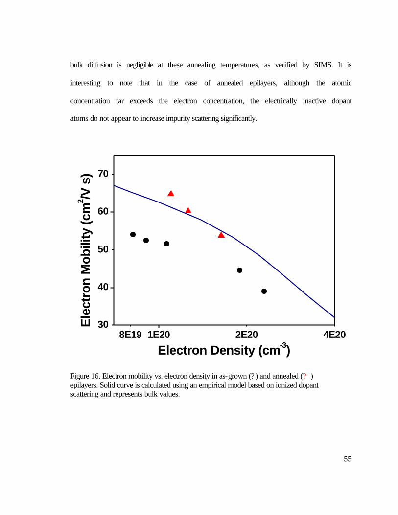
55
bulk diffusion is negligible at these annealing temperatures, as verified by SIMS. It is
interesting to note that in the case of annealed epilayers, although the atomic
concentration far exceeds the electron concentration, the electrically inactive dopant
atoms do not appear to increase impurity scattering significantly.
Figure 16. Electron mobility vs. electron density in as-grown (? ) and annealed (? ) epilayers. Solid curve is calculated using an empirical model based on ionized dopant scattering and represents bulk values.
8E19 1E20 2E20 4E2030
40
50
60
70
Ele
ctro
n M
obili
ty (c
m2 /V
s)
Electron Density (cm-3)
56
4.3.2 MICROSTRUCTURE CHARACTERIZATION
Heavy arsenic doping of silicon by ion implantation, laser annealing or thermal diffusion
is often accompanied by extended defects, such as stacking faults, dislocation loops and
precipitates that can degrade the electrical properties. TEM analyses were performed on
both as-grown and annealed epilayers to investigate the presence of these defects. Figure
17 (a) through (c) show bright-field and high-resolution images of a heavily doped as-
grown epilayer. The rough surface texture observed in Figure 17(b) is consistent with
that observed by AFM and RHEED as shown in Figure 12(a), and appears to be an
undulating variation in the film thickness, but not associated with extended defects within
the epilayer. The {111} lattice fringes are continuous and straight across the epilayer-
substrate interface, indicating that the layer is coherent, and there is no evidence of
arsenic precipitation. Figure 18 shows a high-resolution cross-section image of a similar
sample after in-situ anneal at 730 ºC for 5 minutes. Here one observes a smooth surface,
consistent with AFM and RHEED results shown in Figure 12(b), and again no evidence
of extended defects in the epilayer. TEM analysis on similarly doped samples annealed at
temperatures between 485 and 850 ºC for extended periods also did not indicate the
presence of extended defects.

57
Figure 17. (a) Bright-field cross-section, (b) high-resolution cross-section, and (c) high-resolution plan-view images of as-grown epilayer with an arsenic concentration of 8 × 1020 cm-3. Image in (a) was taken under two-beam conditions using (004) diffracted beam parallel to the film growth direction. (figure continues on next page)
26nm
Epilayer
Substrate
(a)
{111}Planes
10 nm
(b)
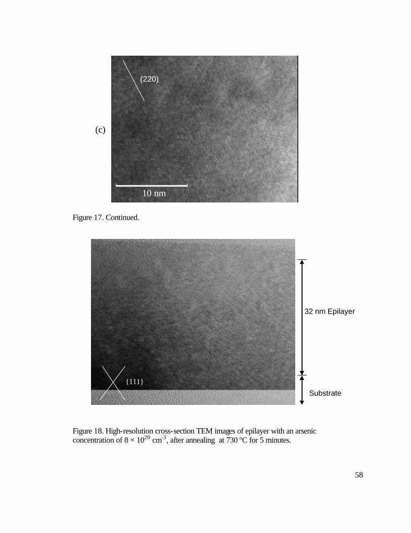
58
Figure 17. Continued.
Figure 18. High-resolution cross-section TEM images of epilayer with an arsenic concentration of 8 × 1020 cm-3, after annealing at 730 ºC for 5 minutes.
(220)
(c)
10 nm
32 nm Epilayer
{111}
Substrate

59
Ion-channeling RBS measurements were performed on both as-grown and annealed
heavily doped epilayers to evaluate arsenic substitutional fraction. The results are listed
in Table 3 and compared with inactive arsenic fractions calculated through Hall and
SIMS measurements. In the as-grown material, there is a significant interstitial
component in the arsenic population, corresponding to 26% of the arsenic occupying
interstitial sites. However, this fraction is much smaller than the fraction of electrically
inactive arsenic. Interstitials are essentially eliminated after annealing, while the inactive
fraction increases further.
Sample Thermal History
Total Arsenic Concentration (cm-3)
Fraction of Interstitial Arsenic
Fraction of Inactive Arsenic
as-grown at 485 ºC 8 × 10²⁰ 26±5% 81.0%
after 730 ºC/5min anneal 8 × 10²⁰ 5±5% 83.6%
Table 3. List of total concentration with substitutional and active fractions of As in as-grown and annealed epilayers.
High-resolution XRD ? -2? scans reveal shifts in the (004) diffraction peak of the
epilayers with respect to that of the substrate, indicating an expansion of the lattice in the
epilayer. The epilayer lattice constant was calculated using
Sin 2
a004 θλ= Equation 6
where a004 is the epilayer lattice constant in the [004] direction, ? is the x-ray wavelength
(0.15406 nm), and ? is the measured diffraction angle. The silicon substrate peak is used

60
to calibrate ?. Assuming the epilayers are coherently strained without relaxation, the
unstrained natural lattice constant a0 is then calculated using
)/C(C21
)a a)/C(C(2 a
1112
004Si11120 ×+
+××= Equation 7
where aSi is the substrate lattice constant, and c11 and c12 are elastic stiffness coefficients.
Because the Si-As material system is a dilute alloy, values for bulk silicon (c11=1.66 and
c12=0.64) [65] are used for this calculation. The relative lattice constant, a0/aSi, is plotted
in Figure 19 as a function of the carrier concentration, for three samples with the same
arsenic concentration, but different degrees of deactivation due to different thermal
history. A decrease in lattice constant is observed with increasing deactivation. It should
be pointed out that all epilayers have thicknesses below the critical thickness values for
their corresponding misfit levels, therefore the coherent strain assumption is justified and
relaxation through generation of misfit dislocations is ruled out as the cause for the
measured change in (004) lattice constant. The absence of misfit dislocations is also
verified by TEM.

61
Figure 19. Relative lattice constant (a0/aSi) vs. carrier concentration for samples with the same arsenic concentration of 8 × 1020 cm-3, but different thermal history.
4.4 DISCUSSION
Because extended defects have been ruled out by TEM, the electrical degradation is most
likely related to atomic-scale clusters and point defects.
1.0x10²⁰ 1.2x10²⁰ 1.4x10²⁰ 1.6x10²⁰ 1.8x10²⁰ 2.0x10²⁰
1.0006
1.0008
1.0010
1.0012
1.0014
1.0016
1.0018
730 oC / 5 minute + 655 oC / 4.3 hour anneal
730 oC / 5 minute anneal
as-growna 0/a
Si:
Rel
ativ
e La
ttic
e C
onst
ant
Carrier Concentration (cm-3)

62
The epilayers were grown at relatively low substrate temperatures with limited surface
diffusion. These conditions are very similar to those used for MBE of heavily antimony-
doped silicon, in which case partially interstitial donor pairs have been observed[61].
Considering the facts that As2 was used as the arsenic source, and that surface arsenic
dimers are energetically stable, it is reasonable to speculate that arsenic-pair-type defects
are incorporated in the as-grown material and contribute to electrical degradation. Low
temperature MBE is known to generate low vacancy densities, typically at the 1015-1016
cm-3 level [66]. Arsenic-termination of the surface further suppresses vacancy formation
[67], therefore enhancement of vacancy incorporation by adding arsenic is not likely. The
lack of vacancies in the as-grown material can suppress the formation of As-V clusters,
which would otherwise dominate arsenic deactivation. According to Chadi’s model [20],
donor pairs become the dominating deactivating defect under such conditions. Because
donor atoms in the pairs are slightly shifted toward each other, they are partially visible
during ion-channeling RBS, consistent with our observations. The difference between
the interstitial arsenic fraction (26%) calculated from ion-channeling RBS and the
electrically inactive fraction (81%) is consistent with the partially interstitial nature of the
defect. These defects also appear to act as additional carrier scattering centers besides
ionized arsenic to degrade electron mobility. The removal of both interstitials and
additional scattering centers by a 730 ºC anneal confirms a link between the two.
Annealing at 730 ºC also reduces the active concentration to equilibrium concentrations
calculated using Berding’s model [62]. The observed changes reflect two simultaneous
processes: disintegration of donor pairs, which releases active arsenic, and formation of
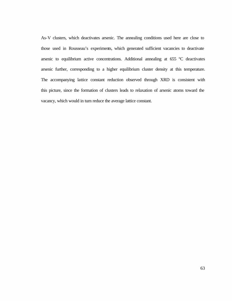
63
As-V clusters, which deactivates arsenic. The annealing conditions used here are close to
those used in Rousseau’s experiments, which generated sufficient vacancies to deactivate
arsenic to equilibrium active concentrations. Additional annealing at 655 ºC deactivates
arsenic further, corresponding to a higher equilibrium cluster density at this temperature.
The accompanying lattice constant reduction observed through XRD is consistent with
this picture, since the formation of clusters leads to relaxation of arsenic atoms toward the
vacancy, which would in turn reduce the average lattice constant.

64
CHAPTER 5: MODULATION DOPING
Discussions so far have been limited to relatively thick, uniformly doped epilayers. A
unique advantage of MBE is the ability to fabricate extremely thin and abrupt chemical
profiles. This chapter discusses processes for generating such arsenic doping profiles and
their unique electrical properties.
5.1 BACKGROUND
As the thickness of a heavily doped layer decreases to the atomic scale, defect
configuration as well as fundamental physics governing its electrical properties can
change dramatically. The extreme of such structures has dopant atoms confined to a
single atomic layer embedded in the host semiconductor, and can be described by the d-
function.
Citrin et al. recently observed an enhancement of dopant activation and reduction of
lattice disorder in antimony-d-doped silicon as compared to similarly doped 3-D layers
[68]. They reasoned that the confinement of dopants in a d-layer reduces the number of
neighboring dopant atoms in the third dimension. As a result donor-pair defect formation
is geometrically suppressed and higher active concentrations can be established. Their
measurements were made exclusively on metastable low-temperature MBE layers
without post-growth anneal. The thermal stability of such an enhancement has yet to be
addressed.
65
The free carrier distribution in silicon depends on the distribution of ionized dopants. In
materials with gradual changes of doping concentration, the free carrier profile follows
the doping profile to a good approximation. However, in d-doped materials which exhibit
large doping concentration variations over short distances, the free carrier distribution is
spread out further than the doping distribution. This is a result of quantum confinement
by the potential well associated with the d-layer. Self-consistent calculations based on the
simultaneous solution of Schrödinger and Poisson equations for d-doped n-type silicon
indicate confinement in a nearly V-shaped potential well, as shown in Figure 20 [69]. The
two occupied energy levels are ground state sub-bands corresponding to the longitudinal
and transverse electron effective masses, respectively. The calculations indicate that the
majority of the electrons occupy the second sub-band, which has a wider spacial extent.
This is related to the smaller transverse effective mass associated with this sub-band.
Because of the quantum confinement, a significant fraction of the electrons are
distributed away from the heavily doped region. The separation of electrons from ionized
scattering centers is expected to greatly enhance electron mobility. Such enhancement has
been observed in antimony and boron d-layers in silicon [70][71], but has not been
reported for arsenic-doped materials.

66
Figure 20. Self-consistent potential (solid line) , level structure and associated densities (dashed lines) and Fermi lavel (short-dashed line) for n-type d-doped silicon, after reference [69].
The separation between neighboring d-layers also appears to have an effect on the carrier
mobility. When two potential wells approach each other, their wavefunctions begin to
overlap, which changes carrier distribution. For p-type doping of silicon with boron, an
apparent enhancement of mobility has been reported for coupled d-layers compared to a
67
single d-layer [70]. For n-type doping with antimony, on the other hand, mobility
enhancement becomes weaker when d-layers are placed in close proximity to each other
[71]. The inconsistency between the two reports is likely a result of different sub-band
structures associated with p- and n-type silicon.
This chapter investigates the above effects in the Si-As material system. Instead of
idealized d-function-like doping spikes, modulation-doped layers with various
thicknesses will be compared. Effects of doping layer thickness as well as spacing
between neighboring doping layers will be discussed.
5.2 GROWTH TECHNIQUE
The modulation-doped structures were grown using a combination of gas- and solid-
silicon sources. While the heavily doped layer requires the exclusive use of solid sources
to facilitate low-temperature growth, undoped layers on either side of the doped layer
were grown using disilane to utilize the higher growth rate.
Before the heavily doped growth, a buffer layer, typically 40 nm thick, is first grown at
655 ºC using disilane. The disilane gas is then stopped and the substrate is cooled to a
lower temperature, typically between 400 and 500 ºC. A modulation-doped layer of the
desired thickness is deposited at this temperature using solid silicon and arsenic sources,
as described in Chapter 3. If multiple doping layers are grown, the arsenic source is
stopped and the substrate is ramped to 655 ºC following the growth of each doped layer.
A spacer layer continues to grow at this higher temperature, which allows equilibrium
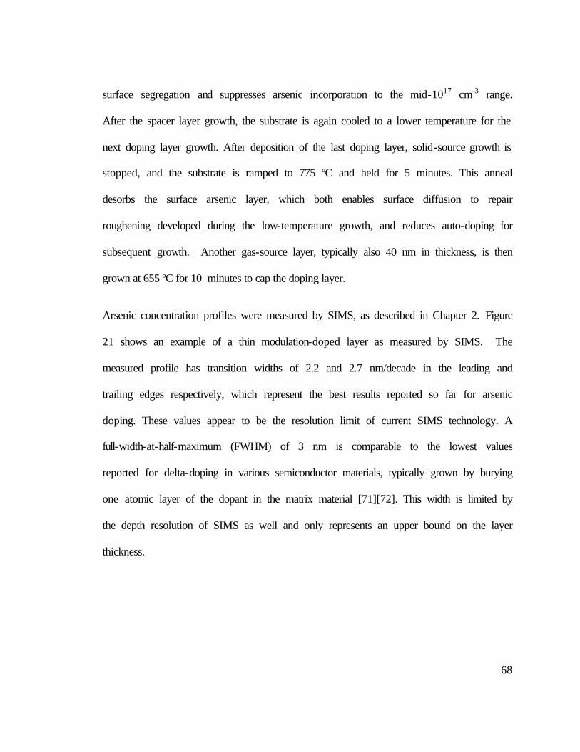
68
surface segregation and suppresses arsenic incorporation to the mid-1017 cm-3 range.
After the spacer layer growth, the substrate is again cooled to a lower temperature for the
next doping layer growth. After deposition of the last doping layer, solid-source growth is
stopped, and the substrate is ramped to 775 ºC and held for 5 minutes. This anneal
desorbs the surface arsenic layer, which both enables surface diffusion to repair
roughening developed during the low-temperature growth, and reduces auto-doping for
subsequent growth. Another gas-source layer, typically also 40 nm in thickness, is then
grown at 655 ºC for 10 minutes to cap the doping layer.
Arsenic concentration profiles were measured by SIMS, as described in Chapter 2. Figure
21 shows an example of a thin modulation-doped layer as measured by SIMS. The
measured profile has transition widths of 2.2 and 2.7 nm/decade in the leading and
trailing edges respectively, which represent the best results reported so far for arsenic
doping. These values appear to be the resolution limit of current SIMS technology. A
full-width-at-half-maximum (FWHM) of 3 nm is comparable to the lowest values
reported for delta-doping in various semiconductor materials, typically grown by burying
one atomic layer of the dopant in the matrix material [71][72]. This width is limited by
the depth resolution of SIMS as well and only represents an upper bound on the layer
thickness.
69
Figure 21. An example of arsenic modulation doping with high concentration and abrupt transitions.
5.3 ELECTRICAL PROPERTIES OF MODULATION-DOPED STRUCTURES
Sheet electron concentration and mobility in modulation-doped layers were obtained
from conductivity and Hall measurements, as described in Chapter 4. To facilitate
comparison with bulk values, the FWHM value from SIMS profiles is taken as the layer
thickness. The 3-D arsenic concentration in the layer is determined by dividing the
integrated arsenic dose in the layer by the FWHM. The equivalent active concentration is
0 20 40 60 80 1001E17
1E18
1E19
1E20
1E21A
rsen
ic C
once
ntra
tion
(cm
-3)
Depth (nm)
70
calculated by dividing the sheet carrier concentration from Hall measurements by the
FWHM. It should be kept in mind that the SIMS FWHM tends to over-estimate the
thickness, especially for thinner layers, which in turn under-estimates 3-D arsenic and
carrier concentrations.
Figure 22 compares electrical activation in samples which have a single modulation-
doped layer of various thicknesses. Because the doping layers have been heat-treated at
775 ºC for 5 minutes during the anneal, and again at 655 ºC for 10 minutes during growth
of the capping layer, equilibrium values for these two temperatures are also plotted for
comparison. 3-D materials with the same thermal history are expected to have an active
concentration in the range between the two curves. This was verified by the sample with
a relatively thick doping layer (FWHM of 16.1 nm). However, as the layer thickness
decreases, an enhancement in activation over equilibrium bulk values is observed, similar
to previous reports on antimony doping [68]. Although the deactivating defect
configuration for the two material systems is different, in both cases neighboring dopant
atoms are needed to form the defect. In the case of arsenic deactivation, the dominating
defect is the As4-V cluster, which requires four arsenic atoms. In the absence of extensive
diffusion, as is the current case, these atoms have to come from nearby regions. With an
arsenic concentration of 1021 cm-3, the average distance between neighboring arsenic
atoms is 1 nm. In a doping layer 3 nm in total thickness, the number of available arsenic
atoms in the direction perpendicular to the doping layer is very limited. This imposes a
geometric constraint on their ability to form clusters and become inactive. The thermal
treatments of the current samples are typical of IC processes. It is speculated that, even

71
with further heat treatment, such an enhancement will be sustained as long as dopant
diffusion is avoided. This stability would be very useful for real device applications.
Figure 22. Data points: active concentration (from Hall measurements) vs. total arsenic concentration (from SIMS) of modulation-doped layers with various thicknesses. Solid lines: Equilibrium values calculated using Berding’s model [62].
Figure 23 plots measured electron mobility vs. active concentration from the same
modulation-doped layers discussed above. While thicker layers exhibit mobility values
consistent with the bulk curve, an enhancement in electron mobility is observed for
doping layers thinner than 5.5 nm. The enhancement is greater for thinner layers,
1E20 1E212E19
4E19
6E198E191E20
2E20
4E20
6E208E201E21
FWHM 16.1 nm
equilibrium
@ 655 o C
equilibrium
@ 775
o C
FWHM 5.5 nm
FWHM 3.7 nm
FWHM 3.0 nm
Act
ive
Con
cent
ratio
n (c
m-3)
Total Arsenic Concentration (cm-3)

72
consistent with the quantum confinement model [69]. When the quantum well width
decreases, sub-band levels become more elevated, which leads to less confinement of the
wavefunctions, corresponding to more electrons distributed away from ionized dopants.
The vast difference between the two data points with FWHM values of 3.7 and 3.0 nm
indicates a strong confinement effect in the latter. The physical thickness of this layer is
likely much smaller, since 3.0 nm represents the lowest limit for SIMS.
Figure 23. Data points: Electron mobilty vs. active concentration of modulation-doped layers with various thicknesses. Solid lines: bulk values calculated using Masetti’s model[64]. Above 5 × 1020 cm-3 bulk values are not established, and the dotted line represents an extrapolation of the existing curve.
1E20 2.5E20 5E20 7.5E201E2120
40
60
80
100
120
FWHM 16.1 nm
FWHM 5.5 nmFWHM 3.7 nm
FWHM 3.0 nm
Ele
ctro
n M
obili
ty (c
m2 /V
s)
Active Concentration (cm-3)
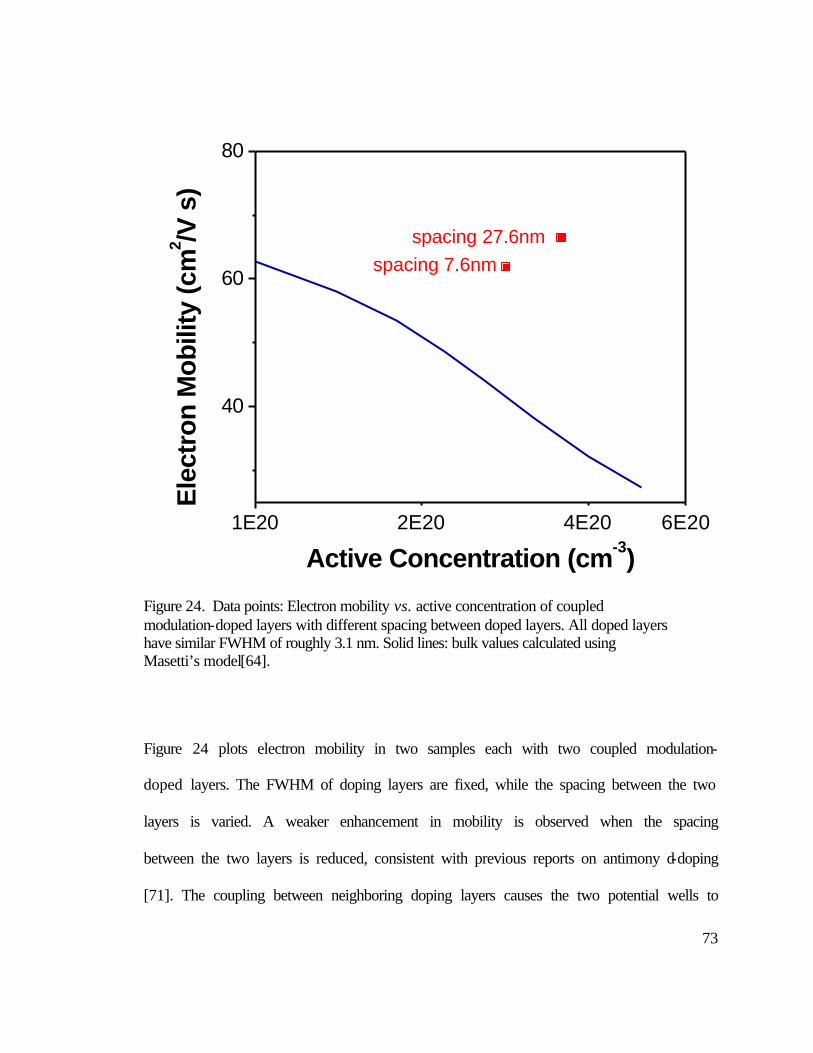
73
Figure 24. Data points: Electron mobility vs. active concentration of coupled modulation-doped layers with different spacing between doped layers. All doped layers have similar FWHM of roughly 3.1 nm. Solid lines: bulk values calculated using Masetti’s model[64].
Figure 24 plots electron mobility in two samples each with two coupled modulation-
doped layers. The FWHM of doping layers are fixed, while the spacing between the two
layers is varied. A weaker enhancement in mobility is observed when the spacing
between the two layers is reduced, consistent with previous reports on antimony d-doping
[71]. The coupling between neighboring doping layers causes the two potential wells to
1E20 2E20 4E20 6E20
40
60
80
spacing 7.6nmspacing 27.6nm
Ele
ctro
n M
obili
ty (c
m2 /V
s)
Active Concentration (cm-3)

74
overlap, which in turn modifies the electron wavefunctions. In this case the modification
appears to increase the electron density in heavily doped regions where Coulombic
scattering occurs. While a detailed calculation is needed to quantify this coupling effect,
calculations based on a single potential well with d-doping levels similar to those used in
this work suggest the spacial extent of electron wavefunctions in the two occupied
ground states to be roughly 5 nm [69]. When the separation between neighboring
potential wells approach this scale, their interaction should be significant, which is
consistent with our observations.
75
CHAPTER 6: SUMMARY AND FUTURE WORK
The incorporation mechanism of arsenic in silicon and SiGe epitaxial layers, as well as
electrical properties of such materials, are important issues for the semiconductor
industry. This dissertation has contributed to the understanding of these topics. In this
chapter we review the major contributions of this dissertation and discuss future avenues
worth exploring.
6.1 SUMMARY
Surface segregation has been a major problem facing dopant incorporation in silicon
epitaxy. The mechanism for arsenic surface segregation was investigated in the absence
of other interfering factors, such as surface hydrogen. Evaluation of the segregation
relations indicated a surface-fraction-dependence of the segregation energy. This
dependence was correlated to 2-D islanding of surface arsenic dimers.
While silicon growth from disilane dictates the use of relatively high substrate
temperatures at which surface segregation prevents effective arsenic incorporation and
reduces the silicon growth rate, much improved arsenic incorporation was achieved in
SiGe as a result of competitive surface segregation between arsenic and germanium.
Addition of germanium also enhances the silicon growth rate by promoting arsenic
desorption. Alternatively, heavy doping of silicon without resorting to adding other
matrix elements can be achieved by utilizing kinetic suppression of surface segregation.

76
Such suppression was realized by using elemental sources combined with lower substrate
temperatures. Extremely high concentrations of arsenic, up to 4×1021 cm-3 and well
beyond the equilibrium solubility limits, were achieved by this method. In the limit of
high arsenic concentrations and kinetic suppression of surface segregation, the addition of
germanium reduces arsenic incorporation. This was attributed to enhanced arsenic
desorption, and possibly other effects, such as solubility and strain.
The high arsenic fractions on the surface and in the bulk of the heavily doped epilayers
appear to exaggerate adverse aspects of low-temperature MBE. A surface roughness
develops during the growth, which was attributed to blocking of surface diffusion routes
by immobile arsenic dimers and islands. The roughening can be repaired by an in-situ
anneal which desorbs the surface arsenic and allows silicon surface diffusion. The critical
epitaxy thickness was also reduced by the addition of arsenic. This effect was attributed
to the presence of high fractions of arsenic both on the surface, where it induces
roughening and nucleates defects, and in the bulk, where it disrupts the lattice through the
introduction of strain and point defects.
Epilayers grown at low temperatures exhibit partial deactivation of incorporated arsenic.
The electron mobility is also degraded, indicating the presence of scattering mechanisms
in addition to Coulombic scattering from ionized arsenic. These effects were tentatively
attributed to partially interstitial donor-pair-type defects formed under the kinetically
limited growth conditions. Annealing recovers the electron mobility to bulk values, but
leads to further deactivation. These effects were attributed to the disintegration of donor

77
pairs and formation of As-V clusters. Microstructure characterization results, as well as
previously reported theoretical calculations, are consistent with these models.
While d-doping studies on other silicon dopants have indicated enhancements in
electrical properties over bulk values, results are inconsistent among different dopants
and are not available for arsenic doping. This work developed growth techniques to
achieve abrupt modulation-doped structures with arsenic. Effects of the doped layer
thickness were studied for the first time, and indicate significant improvements in both
dopant activation and carrier mobility with layer thicknesses below 5.5 nm. The former
was attributed to geometrical suppression of arsenic clustering, and the latter to quantum
confinement effects. Such structures can withstand typical IC thermal processes and have
great potential for device applications. Finally, coupling between neighboring doping
layers was found to modify wavefunctions in a way that reduces carrier mobility. This
effect should be taken into account when the need for low sheet resistance in certain
applications calls for the use of multiple modulation-doped layers.
6.2 SUGGESTIONS FOR FUTURE WORK
6.2.1 SURFACE SEGREGATION ENERGETICS AND KINETICS IN HEAVILY DOPED SILICON
As pointed out in Chapter 3, when surface segregation is kinetically suppressed and
dopant incorporation is significant, other mechanisms, such as Coulombic repulsion,
strain, or band-bending can influence arsenic incorporation. A closer look at the growth
process in this regime is needed to identify and separate these effects. For example, band-
78
bending can be reduced by screening, which is achieved by appropriate background
doping; Strain effects can be addressed by growing a silicon epilayer on relaxed SiGe,
which provides a tensive strain in the Si layer; A wider range of growth rates can be
realized by an E-gun silicon source, to enable more accurate modeling of the rate
processes.
6.2.2 DETAILED ANALYSIS OF ARSENIC INCORPORATION IN SiGe
This dissertation has focused on arsenic incorporation in silicon, and provided very
limited discussion of SiGe. A better understanding of the Si-As system, however, reduces
unknown parameters for the more complicated ternary system. A more detailed study of
the Si:Ge:As material system, using similar techniques to those used for Si-As in this
work, should help provide a better understanding of the interaction between the three
elements.
6.2.3 OPTIMIZATION OF MODULATION DOPING
The current work has explored a very small fraction of modulation doping control
parameters. Further optimization is needed to evaluate its potential for various
applications. It will be interesting to find out, for example, whether modulation doping in
the optimal geometry has an advantage over bulk materials in terms of activation or
mobility, or both. A systematic evaluation of the thermal stability and deactivating rate
processes of such structures would also be beneficial to their device application.

79
6.2.4 ARSENIC DIFFUSION MECHANISM IN SILICON AND SiGe
Arsenic diffusion is closely coupled to point defects. Several models have been proposed
based on mobile As-V clusters [73] or percolation theory [74]. The ability to generate
abrupt modulation doping profiles offers a sensitive method of measuring the
redistribution and diffusion of arsenic during high-temperature growth and post-growth
annealing. The absence of extended defects in these materials also allows one to focus on
point defect mechanisms, as diffusion along extended defects can sometimes be
significant.
80
BIBLIOGRAPHY
[1]. International Technology Roadmap for Semiconductors, 2001 Edition, Front End
Processes (Semiconductor Industry Association, 2001).
[2]. C.K. Date and J.D. Plummer, “Suppression of the Floating-Body Effect Using SiGe
Layers in Vertical Surrounding-Gate MOSFETs”, IEEE Trans. Electron. Dev. 48
(2001) 2684.
[3]. C. Tolksdorf, C. Fink, J. Schulze, S. Sedlmaier, W. Hansch, W. Werner, W. Kanert,
and I. Eisele, “The Vertical Concept of Power MOSFETs”, Mat. Sci. and Eng. B89
(2002) 439.
[4]. H.P. Wong, D.J Frank, and P.M. Solomon, “Device Design Considerations for
Double-Gate, Ground-Plane, and Single-Gated Ultra-Thin SOI MOSFET’s at the 25
nm Chanel Length Generation”, IEDM (1998) 407.
[5]. Y.K. Choi, N. Lindert, P. Xuan, S. Tang, D. Ha, E. Anderson, T.J. King, J. Bokor,
and C. Hu, “Sub-20 nm CMOS FinFET Technologies”, IEDM (2001) 421.
[6]. R.F. Pierret, Semiconductor Fundamentals, 2nd ed., in Modular Series on Solid State
Devices, Vol. 1, Ed. R.F. Pierret and G.W. Neudeck (Addison-Wesley Publishing
Co., Reading, Massachusetts, 1987) p. 34.

81
[7]. D. Nobili, “Solubility of B, P, As and Sb in Si”, EMIS Data Review, (1987), p.384,
394, 410.
[8]. R.B. Fair, “Concentration Profiles of Diffused Dopants in Silicon”, in Impurity
Doping Processes in Silicon, Ed. F.F.Y. Wang (North Holland, Amsterdam, The
Netherlands, 1981) p. 342, 344.
[9]. K.-J. Kramer, S. Talwar, I.T. Lewis, J.E. Davison, K.A. Williams, K.A. Benton, and
K.H. Weiner, “Resistless, Area-Selective Ultrashallow P + /N Junction Fabrication
Using Projection Gas Immersion Laser Doping”, Appl. Phys. Lett. 68 (1996) 2320.
[10]. P.G. Carey, T.W. Sigmon, R.L. Press, and T.S. Fahlen, “Ultra-Shallow High-
Concentration Boron Profiles for CMOS Processing”, IEEE Electron. Dev. Lett. 6
(1985) 291.
[11]. M. Ogirima, H. Saida, M. Sutuki, and M. Maki, “Low Pressure Silicon Epitaxy”, J.
Electrochem. Soc. 124 (1977) 903.
[12]. R. Reif, “Phosphorous Incorporation During Silicon Epitaxy in a CVD Reactor”, J.
Electrochem. Soc. 129 (1982) 1122.
[13]. C. Dominguez and E. Dominguez, “Low Pressure Silicon Epitaxy in a Hot-Wall
Reactor”, Vacuum 37 (1987) 419.

82
[14]. L.P. Chen, G.W. Huang, and C.Y. Chang, “Phosphorus Doping of Si and Si1-x Gex
Grown by Ultrahigh Vacuum Chemical Vapor Deposition Using Si2H6 and GeH4”,
Appl. Phys. Lett. 68 (1996) 1498.
[15]. T. Ohno, “Site Exchange Mechanism in Surfactant-Mediated Epitaxial Growth”,
Phys. Rev. Lett. 73 (1994) 460.
[16]. H. Kim, G. Glass, J.A.N.T. Soares, P. Desjardins, and J.E. Greene, “Arsenic
Incorporation During Si (001): As Gas-Source Molecular-Beam Epitaxy from Si2H6
and AsH3: Effects on Film-Growth Kinetics”, J. Appl. Phys. 88 (2000) 7067.
[17]. J.H. Comfort, and R. Rief, “Plasma-Enhanced Chemical Vapor Deposition of in-
situ Doped Epitaxial Silicon at Low Temperatures. I. Arsenic Doping”, J. Appl.
Phys. 65 (1989) 1053.
[18]. H.-J. Gossmann, F.C. Unterwald, and H.S. Luftman, “Doping of Si Thin Films by
Low-Temperature Molecular Beam Epitaxy”, J. Appl. Phys. 73 (1993) 8237.
[19]. H. Jorke, “Surface Segregation of Sb on Si (100) During Molecular Beam Epitaxy
Growth”, Surf. Sci. 193 (1988) 569.
[20]. D.J. Chadi, P.H. Citrin, C.H. Park, D.L. Adler, M.A. Marcus and H.-J. Gosmann,
“Fermi-Level-Pinning Defects in Highly n-Doped Silicon”, Phys. Rev. Lett. 79
(1997) 4834.

83
[21]. O.D. Dubon, P.G. Evans, J.F. Chervinsky, M.J. Aziz, F. Spaepen, M.F. Chisholm,
and D.A. Muller, “Doping by Metal-Mediated Epitaxy: Growth of As Delta-Doped
Si Through a Pb Monolayer”, Appl. Phys. Lett. 78 (2001) 1505.
[22]. G.J. Davies and D. Williams, “III-V MBE Growth Systems”, in The Technology
and Physics of Molecular Beam Epitaxy, Ed. E. H. C. Parker (Plenum Press, New
York, 1985).
[23]. T.I Kamins and D. Lefforge, “Control of n-type Dopant Transitions in Low-
Temperature Silicon Epitaxy”, J. Electrochem. Soc. 144 (1997) 674.
[24]. R.W. Price, E.S. Tok, and J. Zhang, “Probing the Disilane Adsorption Kinetics: As
Alternative Approach”, Phys. Rev. B 59 (1999) R5292.
[25]. T.R. Bramblett, Q. Lu, T. Karasawa, M.-A. Hasan, S.K. Jo, and J.E. Greene, “Si
(001) 2x1 Gas-Source Molecular-Beam Epitaxy from Si2H6: Growth Kinetics and
Boron Doping”, J. Appl. Phys. 76 3 (1994) 1884.
[26]. M.-H. Xie, A.K. Lees, J.M. Fernandez, J. Zhang, and B.A. Joyce, “Arsenic Surface
Segregation and Incorporation in Si and Si1-xGex During Gas Source Molecular
Beam Epitaxy”, J. Crystal Growth 173 (1997) 336.
[27]. J.J. Harris, D.E. Ashenford, C.T. Foxon, P.J. Dobson and B.A. Joyce, “Kinetic
Limitations to Surface Segregation during MBE Growth of III-V Compounds - Sn
in GaAs”, Appl. Phys. A-Materials Science & Processing 33 (1984) 87.

84
[28]. S.A. Barnet and J.E. Greene, “Si Molecular Beam Epitaxy: a Model for
Temperature Dependent Incorporation Probabilities and Depth Distributions of
Dopants Exhibiting Strong Surface Segregation”, Surf. Sci. 151 (1985) 67.
[29]. R.I.G. Uhrberg, R.D. Bringans, R.Z. Bachrach, and J.E. Northrup, “Symmetric
Arsenic Dimers on the Si (100) Surface, Phys. Rev. Lett. 56 (1986) 520.
[30]. A.D. Hartell, E.S. Tok, and J. Zhang, “The Development of RAS and RHEED as
in-situ Probes to Monitor Dopant Segregation in GS-MBE on SI (001)”, J. Crystal
Growth 227-228 (2001) 729.
[31]. A.L. Alstrin, P.G. Strupp, and S.R. Leone, “Direct Detection of Atomic Arsenic
Desorption From Si (100)”, Appl. Phys. Lett. 63 (1993) 815.
[32]. E.S. Tok, A.D. Hartell and J.Zhang, “Kinetics of Si Growth From Hydride
Precursors on As-Passivated Si (001) Surface”, Appl. Phys. Lett. 78 (2001) 919.
[33]. L. Kipp, R.D. Bringans, D.K. Biegelsen and L.-E. Swartz, “Arsine Adsorption on Si
(100) 2 x 1: A Photoemission and Scanning-Tunneling-Microscopy Study”, Phys.
Rev. B 50 (1994) 5448.
[34]. E.S. Tok, N.J. Woods, and J. Zhang, “RHEED and SIMS Studies of Germanium
Segregation During Growth and SiGe/Si Heterostructures: A Two-Site Exchange
Model with Growth Rate Dependence”, J. Crystal Growth 209 (2000) 321.

85
[35]. B.S. Meyerson, K.J. Uram, and F.K. LeGoues, “Cooperative Growth Phenomina in
Silicon/Germanium Low-Temperature Epitaxy”, Appl. Phys. Lett. 53 (1988) 2555.
[36]. C.L. Berrie and S.R. Leone, “Desorption of Arsenic Species During the Surfactant
Enhanced Growth of Ge on Si (100)”, J. Phys. Chem. B 106 (2002) 6488.
[37]. S. Spruytte, C. Coldren, J. Harris, D. Pantelidis, H.-J. Lee, J. Bravman, and M.
Kelly, “Use of Angle Resolved X-Ray Photoelectron Spectroscopy for
Determination of Depth and Thickness of Compound Layer Structures”, J. Vac. Sci.
Technol. A 19 (2) (2001) 603.
[38]. SSI S-Probe Monochromatized XPS Spectrometer software default values.
[39]. G. Sommerjai, Chemistry in Two Dimensions: Surfaces (Cornell University Press,
Ithaca, NY, 1981).
[40]. K. Suzuki, H. Tashiro, and Y. Aoyama, “Time Evolution of the Resistance of
Arsenic, Phosphorous, and Boron-Doped Crystalline Silicon”, J. Electrochem. Soc.
149 (2002) G175.
[41]. E.F. Schubert, G.H. Gilmer, R.F. Kopf and H.S. Luftman, “Maximum
Concentration of Impurities in Semiconductors”, Phys. Rev. B 46 (1992) 15078.
[42]. E.F. Schubert, J.M. Kuo, R.F. Kopf, A.S. Jordan, H.S. Luftman and L.C. Hopkins,
“Fermi-Level-Pinning-Induced Impurity Redistribution in Semiconductors During
Epitaxial Growth”, Phys. Rev. B 42 (1990) 1364.

86
[43]. W.J. Edwards, Y.-S. Chein, S.Lin, D.G. Ast, P. Krusius, and T.I. Kamins, “Dopant
Implantation and Activation in Polycrystalline SiGe”, Mater. Res. Soc. Symp. Proc.
343 (1994) 685.
[44]. A. Lietolia, J.F. Gibbons and T.W. Sigmon, “The Solid Solubility and Thermal
Behavior of Metastable Concentration of As in Si”, Appl. Phys. Lett. 36 (1980) 765.
Confirm.
[45]. A.I. Nikiforov, B.Z. Kanter, and O.P. Pchelyakov, “RHEED Investigation of
Limiting Thickness Epitaxy During Low-Temperature Si–MBE on (100) Surface”,
Thin Solid Films 336 (1998) 179.
[46]. D.J. Eaglesham, “Semiconductor Moledular-Beam Epitaxy at Low Temperatures”,
J. Appl. Phys. 77 (1995) 3597.
[47]. J. Thiesen, H.M. Branz, and R.S. Crandall, “Explanation of the Limiting Thickness
Observed in Low-Temperature Silicon Epitaxy”, Appl. Phys. Lett. 77 (2000) 3589.
[48]. P. Asoka-Kumar, S. Szpala, B. Nielsen, Cs. Szeles, and K.G. Lynn, “Hydrogen-
Induced Breakdown of Low-Temperature Molecular-Beam Epitaxy of Si”, Phys.
Rev. B 51 (1995) 4630.
[49]. D.J. Eaglesham, H.-J. Gosmann, and M. Cerullo, “Limiting Thickness hepi for
Epitaxial Growth and Room-Temperature Si Growth on Si (100)”, Phys. Rev. Lett.
65 (1990) 1227.
87
[50]. M.V.R. Murty and H.A. Atwater, “Very Low Temperature (<400 °C) Silicon
Molecular Beam Epitaxy: The Role of Low Energy Ion Irradiation”, Appl. Phys.
Lett. 62 (1994) 2566.
[51]. W.J. Vahue, J.L. Rodgers, P.S. Audrey, and E. Adams, “Epitaxial Film Thickness
in the Low-Temperature Growth of Si(100) by Plasma Enhanced Chemical Vapor
Deposition”, Appl. Phys. Lett. 68 (1996) 349.
[52]. A. Armigliato, D. Nobili, and S. Solmi, “Electron Microscopy of As Supersaturated
Silicon”, J. Electrochem. Soc. 133 (1986) 2560.
[53]. A. Parsini, A. Bourret, A. Armigliato, M. Servidori, S. Solmi, and R. Fabbri,
“Electrical Activity and Structural Evolution Correlations in Laser and Thermally
Annealed As-Implanted Si Specimens”, J. Appl. Phys. 67 (1990) 2320.
[54]. O. Dokumaci, P. Rousseau, S. Luning, V. Krishnamoorthy, K.S. Jones, and M.E.
Law, “Transmission Electron Microscopy Analysis of Heavily As-Doped, Laser,
and Thermally Annealed Layers in Silicon”, J. Appl. Phys. 78 (1995) 828.
[55]. Y. Komem, “An Electron Microscopy Study of Arsenic Segregration in Silicon”,
Acta Metalurgica 25 (1977) 809.
[56]. W.K. Chu and B.J. Masters, “Laser-Solid Interactions and Laser Processing”, AIP
Conf. Proc. No. 50, et. S.D. Ferris, H.J. Leamy and J.M. Poate (AIP, New York,
1979) p. 305.
88
[57]. K.C. Pandey, A. Erbil, G.S. Cargill, R.F. Boehme, and D. Vanderbilt, “Annealing
of Heavily Arsenic-Doped Silicon: Electrical Deactivation and a New Defect
Complex”, Phys. Rev. Lett. 61 (1988) 1282.
[58]. J.L. Allain, J.R. Regnard, A. Bourret, A. Parisini, A. Armigiliato, g. Tourillon, and
S. Pizzini, “Extended X-Ray-Absorption Fine-Structure Study of The Local Atomic
Structure in As+ Heavily Implanted Silicon”, Phys. Rev. B 46 (1992) 9434.
[59]. P.M. Rousseau, P.B. Griffin, and J.D. Plummer, “Vacancy Generation Resulting
from Electrical Deactivation of Arsenic”, Appl. Phys. Lett. 67 (1995) 3575.
[60]. U. Myler, P.J. Simpson, D.W. Lawther, and P.M. Rousseau, “On the Electrical
Deactivation of Arsenic in Silicon”, J. Vac. Sci. Technol, B 15 (1997) 757.
[61]. P.M. Voyles, D.A. Muller, J.L. Grazul, P.H. Citrin, and H.-J. Gossmann, “Atomic-
Scale Imaging of Individual Dopant Atoms and Clusters in Highly n-Type Bulk Si”,
Nature 416 (2002) 826.
[62]. M.A. Berding and A. Sher, “Electronic Quasichemical Formalism: Application to
Arsenic Deactivation in Silicon”, Phys. Rev. B 58 (1998) 3853.
[63]. F. Mousty, P. Ostoja, and L. Passari, “Relationship between Resistivity and
Phosphorous Concentration in Silicon”, J. Appl. Phys. 45 (1974) 4576.
89
[64]. G. Masetti, M. Severi, and S. Solmi, “Modeling of Carrier Mobility Against Carrier
Concentration in Arsenic-, Phosphorous-, and Boron-Doped Silicon”, IEEE Trans.
Electron devices Ed-30 (1983) 764.
[65]. J.J.Wortman, “Young's Modulus, Shear Modulus, and Poisson's Ratio in SIlicon
and Germanium”, J. Appl. Phys. 36 (1965) 153.
[66]. H.-J. Gossmann, P. Asoka-Kumar, T.C. Leung, B. Nielsen, K.G. Lynn, F.C.
Unterwald, and L.C. Feldman, “Point Defects in Si Thin Films Grown by Molecular
Beam Epitaxy”, Appl. Phys. Lett. 61 (1992) 540.
[67]. M. Ramamoorthy, E.L. Briggs, and J. Bernhole, “Defect Energetics and Impurity
Incorporation Mechanisms at the Arsenic-Passivated Si (100) Surface”, Phys. Rev.
B 60 (1999) 8178.
[68]. P.H. Citrin, D.A. Muller, H.-J. Gossmann, R. Vanfleet, and P.A. Northrup,
“Geometric Frustration of 2D Dopants in Silicon: Surpasing Electrical Saturation”,
Phys. Rev. Lett. 83 (1999) 3234.
[69]. C.R. Proetto, “Electrnic Structure of Delta-Doped Semiconductors”, in Delta-
Doping of Semiconductors, Ed. E.F. Schubert (Cambridge University Press, 1996)
p.55.
[70]. T.K. Carns, X. Zheng, and K.L. Wang, “Enhancement of Si Hole Mobility in
Coupled Delta-Doped Wells”, Appl. Phys. Lett. 62 (1993) 3455.
90
[71]. H.-J. Gossmann and F.C. Unterwald, “Dopant Electrical Activity and Majority-
Carrier Mobility in B- and Sb-Delat-Doped Si Thin Films”, Phys. Rev. B 47 (1993)
12618.
[72]. E.F. Schubert, in Delta-Doping of Semiconductors, Ed. E.F. Schubert (Cambridge
University Press, 1996) p. 10.
[73]. M. Ramamoorthy and S.T. Pantelides, “Complex Dynamical Phenomena in Heavily
Arsenic Doped Silicon”, Phys. Rev. Lett. 76 (1996) 4753.
[74]. J. Xie and S.P. Chen, “Diffusion and Clustering in Heavily Arsenic-Doped Silicon:
Discrepancies and Explanation”, Phys. Rev. Lett. 83 (1999) 1795.