armv8-a aarch64 isa overview - microsoft you more about a64, an instruction set which is going to be...
TRANSCRIPT

64-bit Android on ARM, Campus London, September 20150839 rev 12368 1
ARMv8-A A64 ISA Overview
presented by
Matteo Franchin <[email protected]>

64-bit Android on ARM, Campus London, September 20150839 rev 12368 2
Agenda
Introduction
Registers
Loads and stores
Data processing and control flow
Scalar floating-point and SIMD
64-bit Android on ARM, Campus London, September 20150839 rev 12368 3
Motivation
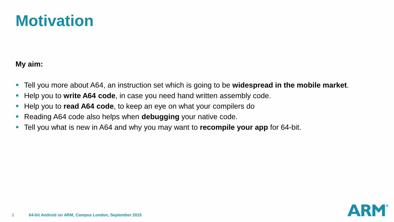
My aim:
Tell you more about A64, an instruction set which is going to be widespread in the mobile market.
Help you to write A64 code, in case you need hand written assembly code.
Help you to read A64 code, to keep an eye on what your compilers do
Reading A64 code also helps when debugging your native code.
Tell you what is new in A64 and why you may want to recompile your app for 64-bit.

64-bit Android on ARM, Campus London, September 20150839 rev 12368 4
Introduction
This is a general introduction to the A64 instruction set
But does not cover all available instructions
Does not detail all forms, options, and restrictions for each instruction
For more information, see the following on infocenter.arm.com:
ARMv8-A Architecture Reference Manual. Document number: DDI 0487
ARM® Compiler 6 armasm Reference Guide. Document number: DUI 0802
Has an A-Z listing of all available instructions and can be easier to digest than the ARMv8-A Architecture Reference Manual
ARM Architecture Procedure Call Standard for 64-bit (AAPCS64). Document number IHI 0055B
How registers are used by compilers, how arguments are passed, etc.
For presentations on 64-bit Android on ARM see:
LCU14-504: Taming ARMv8 NEON: from theory to benchmark results – YouTube: Using NEON™ in native code
HKG15-300: Art's Quick Compiler: An unofficial overview – YouTube: A64 support in the Android Java runtime
LCU14-100: Dalvik is Dead, Long Live Dalvik! OR Tuning ART – YouTube: Porting Android to 64-bit ARM
More Presentations on Porting to 64-bit
64-bit Android on ARM, Campus London, September 20150839 rev 12368 5
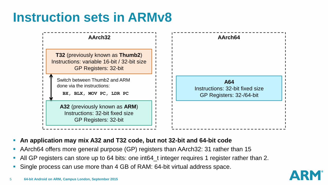
An application may mix A32 and T32 code, but not 32-bit and 64-bit code
AArch64 offers more general purpose (GP) registers than AArch32: 31 rather than 15
All GP registers can store up to 64 bits: one int64_t integer requires 1 register rather than 2.
Single process can use more than 4 GB of RAM: 64-bit virtual address space.
Instruction sets in ARMv8
T32 (previously known as Thumb2)
Instructions: variable 16-bit / 32-bit size
GP Registers: 32-bit
A32 (previously known as ARM)
Instructions: 32-bit fixed size
GP Registers: 32-bit
A64
Instructions: 32-bit fixed size
GP Registers: 32-/64-bit
AArch32 AArch64
Switch between Thumb2 and ARM
done via the instructions:
BX, BLX, MOV PC, LDR PC
64-bit Android on ARM, Campus London, September 20150839 rev 12368 6
Agenda
Introduction
Registers
Loads and stores
Data processing and control flow
Scalar floating-point and SIMD
64-bit Android on ARM, Campus London, September 20150839 rev 12368 7
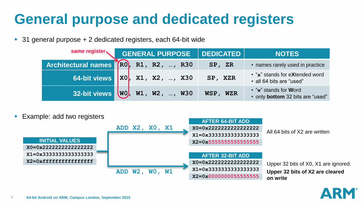
General purpose and dedicated registers
31 general purpose + 2 dedicated registers, each 64-bit wide
Example: add two registers
GENERAL PURPOSE DEDICATED NOTES
Architectural names R0, R1, R2, …, R30 SP, ZR • names rarely used in practice
64-bit views X0, X1, X2, …, X30 SP, XZR • “x” stands for eXtended word
• all 64 bits are “used”
32-bit views W0, W1, W2, …, W30 WSP, WZR • “w” stands for Word
• only bottom 32 bits are “used”
same register
INITIAL VALUES
X0=0x2222222222222222
X1=0x3333333333333333
X2=0xffffffffffffffff
AFTER 64-BIT ADD
X0=0x2222222222222222
X1=0x3333333333333333
X2=0x5555555555555555
AFTER 32-BIT ADD
X0=0x2222222222222222
X1=0x3333333333333333
X2=0x0000000055555555
ADD X2, X0, X1
Upper 32 bits of X0, X1 are ignored.
Upper 32 bits of X2 are cleared
on write
All 64 bits of X2 are written
ADD W2, W0, W1
AFTER 64-BIT ADD
X0=0x2222222222222222
X1=0x3333333333333333
X2=0x5555555555555555
AFTER 32-BIT ADD
X0=0x2222222222222222
X1=0x3333333333333333
X2=0x0000000055555555
64-bit Android on ARM, Campus London, September 20150839 rev 12368 8
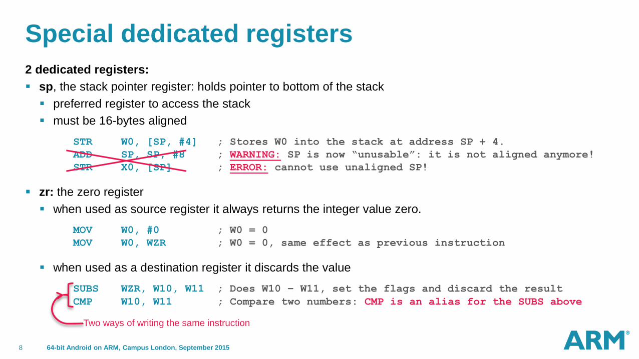
Special dedicated registers
2 dedicated registers:
sp, the stack pointer register: holds pointer to bottom of the stack
preferred register to access the stack
must be 16-bytes aligned
STR W0, [SP, #4] ; Stores W0 into the stack at address SP + 4.
ADD SP, SP, #8 ; WARNING: SP is now “unusable”: it is not aligned anymore!
STR X0, [SP] ; ERROR: cannot use unaligned SP!
zr: the zero register
when used as source register it always returns the integer value zero.
MOV W0, #0 ; W0 = 0
MOV W0, WZR ; W0 = 0, same effect as previous instruction
when used as a destination register it discards the value
SUBS WZR, W10, W11 ; Does W10 – W11, set the flags and discard the result
CMP W10, W11 ; Compare two numbers: CMP is an alias for the SUBS above
Two ways of writing the same instruction
64-bit Android on ARM, Campus London, September 20150839 rev 12368 9
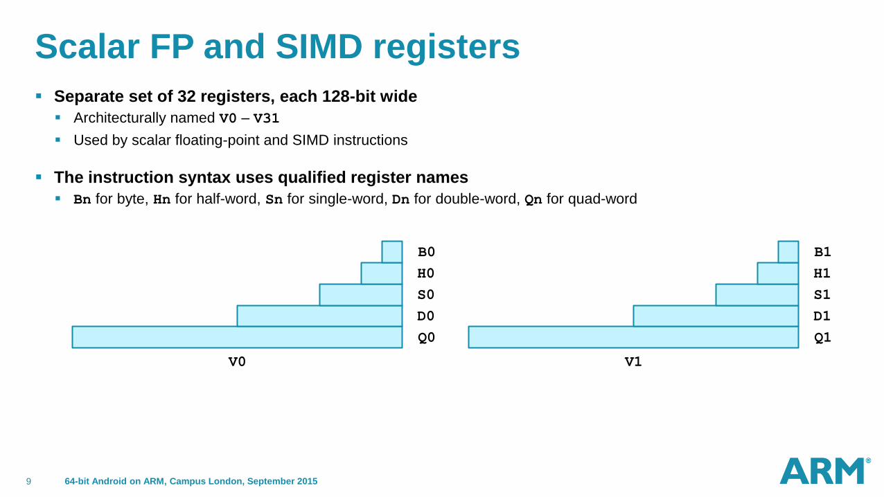
Scalar FP and SIMD registers
Separate set of 32 registers, each 128-bit wide
Architecturally named V0 – V31
Used by scalar floating-point and SIMD instructions
The instruction syntax uses qualified register names
Bn for byte, Hn for half-word, Sn for single-word, Dn for double-word, Qn for quad-word
B0
H0
S0
D0
Q0
B1
H1
S1
D1
Q1
V0 V1
64-bit Android on ARM, Campus London, September 20150839 rev 12368 10
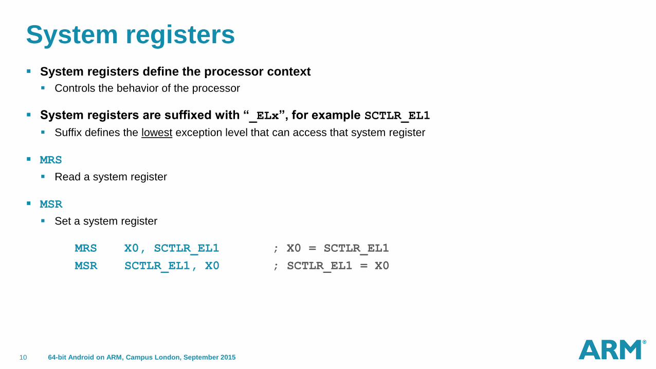
System registers
System registers define the processor context
Controls the behavior of the processor
System registers are suffixed with “_ELx”, for example SCTLR_EL1
Suffix defines the lowest exception level that can access that system register
MRS
Read a system register
MSR
Set a system register
MRS X0, SCTLR_EL1 ; X0 = SCTLR_EL1
MSR SCTLR_EL1, X0 ; SCTLR_EL1 = X0

64-bit Android on ARM, Campus London, September 20150839 rev 12368 11
Agenda
Introduction
Registers
Loads and stores
Data processing and control flow
Scalar floating-point and SIMD
64-bit Android on ARM, Campus London, September 20150839 rev 12368 12
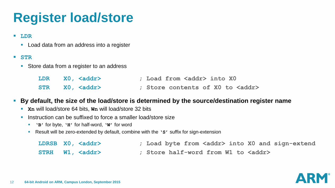
Register load/store
LDR
Load data from an address into a register
STR
Store data from a register to an address
LDR X0, <addr> ; Load from <addr> into X0
STR X0, <addr> ; Store contents of X0 to <addr>
By default, the size of the load/store is determined by the source/destination register name
Xn will load/store 64 bits, Wn will load/store 32 bits
Instruction can be suffixed to force a smaller load/store size
‘B’ for byte, ‘H’ for half-word, ‘W’ for word
Result will be zero-extended by default, combine with the ‘S’ suffix for sign-extension
LDRSB X0, <addr> ; Load byte from <addr> into X0 and sign-extend
STRH W1, <addr> ; Store half-word from W1 to <addr>
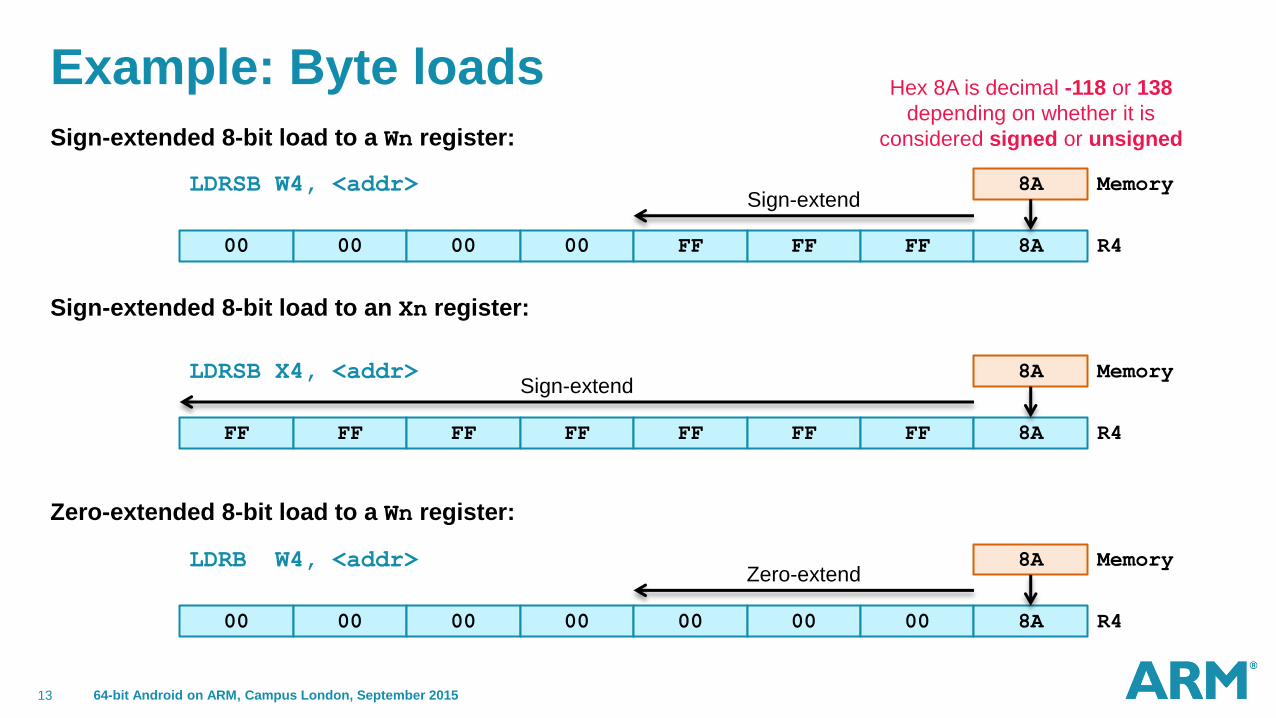
64-bit Android on ARM, Campus London, September 20150839 rev 12368 13
Example: Byte loads
00 00 00 00 FF FF FF 8A
8A
FF FF FF FF FF FF FF 8A
8A
00 00 00 00 00 00 00 8A
8A
Memory
R4
Memory
R4
Memory
R4
Sign-extend
Sign-extend
Zero-extend
LDRSB W4, <addr>
LDRSB X4, <addr>
LDRB W4, <addr>
Sign-extended 8-bit load to a Wn register:
Sign-extended 8-bit load to an Xn register:
Zero-extended 8-bit load to a Wn register:
Hex 8A is decimal -118 or 138
depending on whether it is
considered signed or unsigned
64-bit Android on ARM, Campus London, September 20150839 rev 12368 14
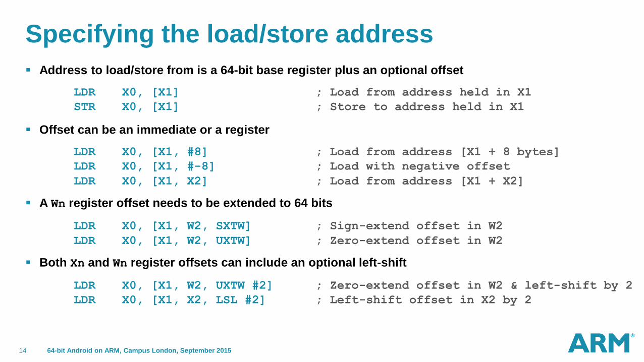
Specifying the load/store address
Address to load/store from is a 64-bit base register plus an optional offset
LDR X0, [X1] ; Load from address held in X1
STR X0, [X1] ; Store to address held in X1
Offset can be an immediate or a register
LDR X0, [X1, #8] ; Load from address [X1 + 8 bytes]
LDR X0, [X1, #-8] ; Load with negative offset
LDR X0, [X1, X2] ; Load from address [X1 + X2]
A Wn register offset needs to be extended to 64 bits
LDR X0, [X1, W2, SXTW] ; Sign-extend offset in W2
LDR X0, [X1, W2, UXTW] ; Zero-extend offset in W2
Both Xn and Wn register offsets can include an optional left-shift
LDR X0, [X1, W2, UXTW #2] ; Zero-extend offset in W2 & left-shift by 2
LDR X0, [X1, X2, LSL #2] ; Left-shift offset in X2 by 2
64-bit Android on ARM, Campus London, September 20150839 rev 12368 15
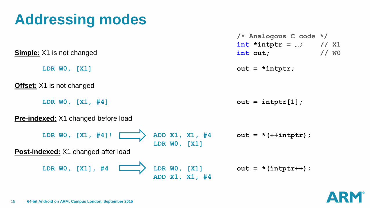
/* Analogous C code */
int *intptr = …; // X1
Simple: X1 is not changed int out; // W0
LDR W0, [X1] out = *intptr;
Offset: X1 is not changed
LDR W0, [X1, #4] out = intptr[1];
Pre-indexed: X1 changed before load
LDR W0, [X1, #4]! ADD X1, X1, #4 out = *(++intptr);
LDR W0, [X1]
Post-indexed: X1 changed after load
LDR W0, [X1], #4 LDR W0, [X1] out = *(intptr++);
ADD X1, X1, #4
Addressing modes
64-bit Android on ARM, Campus London, September 20150839 rev 12368 16
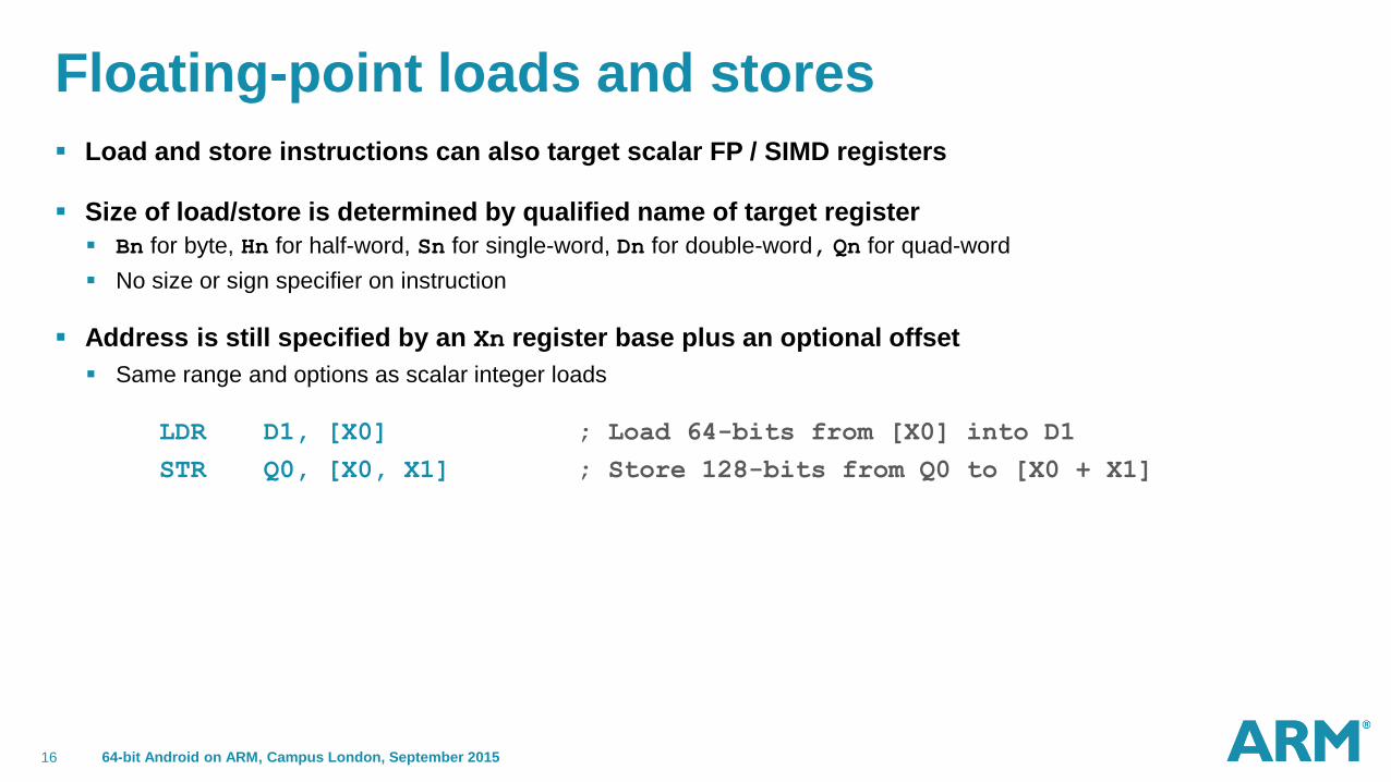
Floating-point loads and stores
Load and store instructions can also target scalar FP / SIMD registers
Size of load/store is determined by qualified name of target register
Bn for byte, Hn for half-word, Sn for single-word, Dn for double-word, Qn for quad-word
No size or sign specifier on instruction
Address is still specified by an Xn register base plus an optional offset
Same range and options as scalar integer loads
LDR D1, [X0] ; Load 64-bits from [X0] into D1
STR Q0, [X0, X1] ; Store 128-bits from Q0 to [X0 + X1]
64-bit Android on ARM, Campus London, September 20150839 rev 12368 17
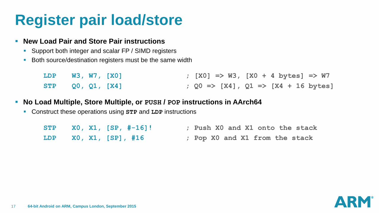
Register pair load/store
New Load Pair and Store Pair instructions
Support both integer and scalar FP / SIMD registers
Both source/destination registers must be the same width
LDP W3, W7, [X0] ; [X0] => W3, [X0 + 4 bytes] => W7
STP Q0, Q1, [X4] ; Q0 => [X4], Q1 => [X4 + 16 bytes]
No Load Multiple, Store Multiple, or PUSH / POP instructions in AArch64
Construct these operations using STP and LDP instructions
STP X0, X1, [SP, #-16]! ; Push X0 and X1 onto the stack
LDP X0, X1, [SP], #16 ; Pop X0 and X1 from the stack
64-bit Android on ARM, Campus London, September 20150839 rev 12368 18
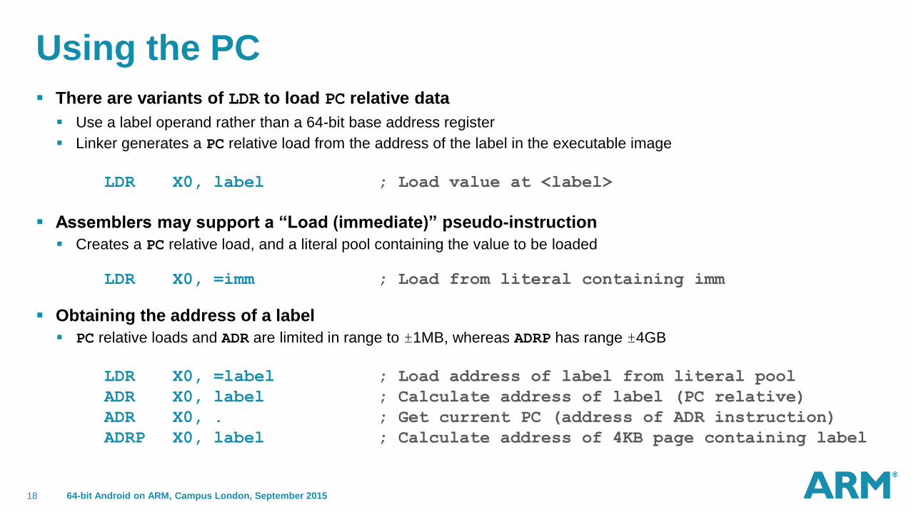
Using the PC
There are variants of LDR to load PC relative data
Use a label operand rather than a 64-bit base address register
Linker generates a PC relative load from the address of the label in the executable image
LDR X0, label ; Load value at <label>
Assemblers may support a “Load (immediate)” pseudo-instruction
Creates a PC relative load, and a literal pool containing the value to be loaded
LDR X0, =imm ; Load from literal containing imm
Obtaining the address of a label
PC relative loads and ADR are limited in range to ±1MB, whereas ADRP has range ±4GB
LDR X0, =label ; Load address of label from literal pool
ADR X0, label ; Calculate address of label (PC relative)
ADR X0, . ; Get current PC (address of ADR instruction)
ADRP X0, label ; Calculate address of 4KB page containing label
64-bit Android on ARM, Campus London, September 20150839 rev 12368 19
Agenda
Introduction
Registers
Loads and stores
Data processing and control flow
Scalar floating-point and SIMD
64-bit Android on ARM, Campus London, September 20150839 rev 12368 20
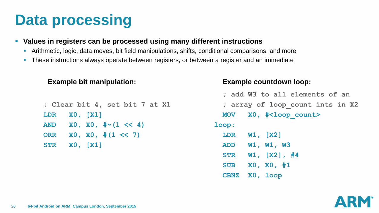
Data processing
Values in registers can be processed using many different instructions
Arithmetic, logic, data moves, bit field manipulations, shifts, conditional comparisons, and more
These instructions always operate between registers, or between a register and an immediate
Example bit manipulation: Example countdown loop:
; add W3 to all elements of an
; Clear bit 4, set bit 7 at X1 ; array of loop_count ints in X2
LDR X0, [X1] MOV X0, #<loop_count>
AND X0, X0, #~(1 << 4) loop:
ORR X0, X0, #(1 << 7) LDR W1, [X2]
STR X0, [X1] ADD W1, W1, W3
STR W1, [X2], #4
SUB X0, X0, #1
CBNZ X0, loop
64-bit Android on ARM, Campus London, September 20150839 rev 12368 21
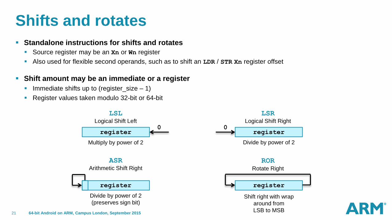
Shifts and rotates
Standalone instructions for shifts and rotates
Source register may be an Xn or Wn register
Also used for flexible second operands, such as to shift an LDR / STR Xn register offset
Shift amount may be an immediate or a register
Immediate shifts up to (register_size – 1)
Register values taken modulo 32-bit or 64-bit
register
register
register
register
Multiply by power of 2 Divide by power of 2
Divide by power of 2
(preserves sign bit) Shift right with wrap
around from
LSB to MSB
0 0
LSL Logical Shift Left
LSR Logical Shift Right
ASR Arithmetic Shift Right
ROR Rotate Right

64-bit Android on ARM, Campus London, September 20150839 rev 12368 22
These are just some examples, there are many more bit manipulation instructions
Bit manipulation (1)
0 0 0 0 0 0 0 0 1 0 1 0 1 1 0 0 0 1 0 0 1 1 1 0 0 1 1 0 1 0
0 0 0 0 0 0 0 1 0 1 0 1 0 0 0 1 0 1 0 0 0 1 1 1 0 1 0 0
0 0 0 0 0 0 0 0 0 0 0 0 0 0 0 0 0 0 0 0 0 0 0 0 0 1 0 1 0 1
0 0 0 0 0 0 0 0 0 0 0 0 0 0 0 0 0 0 0 0 0 0 0 0 0 0 1 1
0 31
31
31
31
0
0
0
W0
W0
W1
W1
BFI W0, W0, #9, #6 ; Bit Field Insert
UBFX W1, W0, #18, #7 ; Bit Field Extract
BFI W1, WZR, #3, #4 ; Bit Field Clear 0 0 WZR
1 0
0 1 1 0
0 1
0 0
0 0 0 0
64-bit Android on ARM, Campus London, September 20150839 rev 12368 23
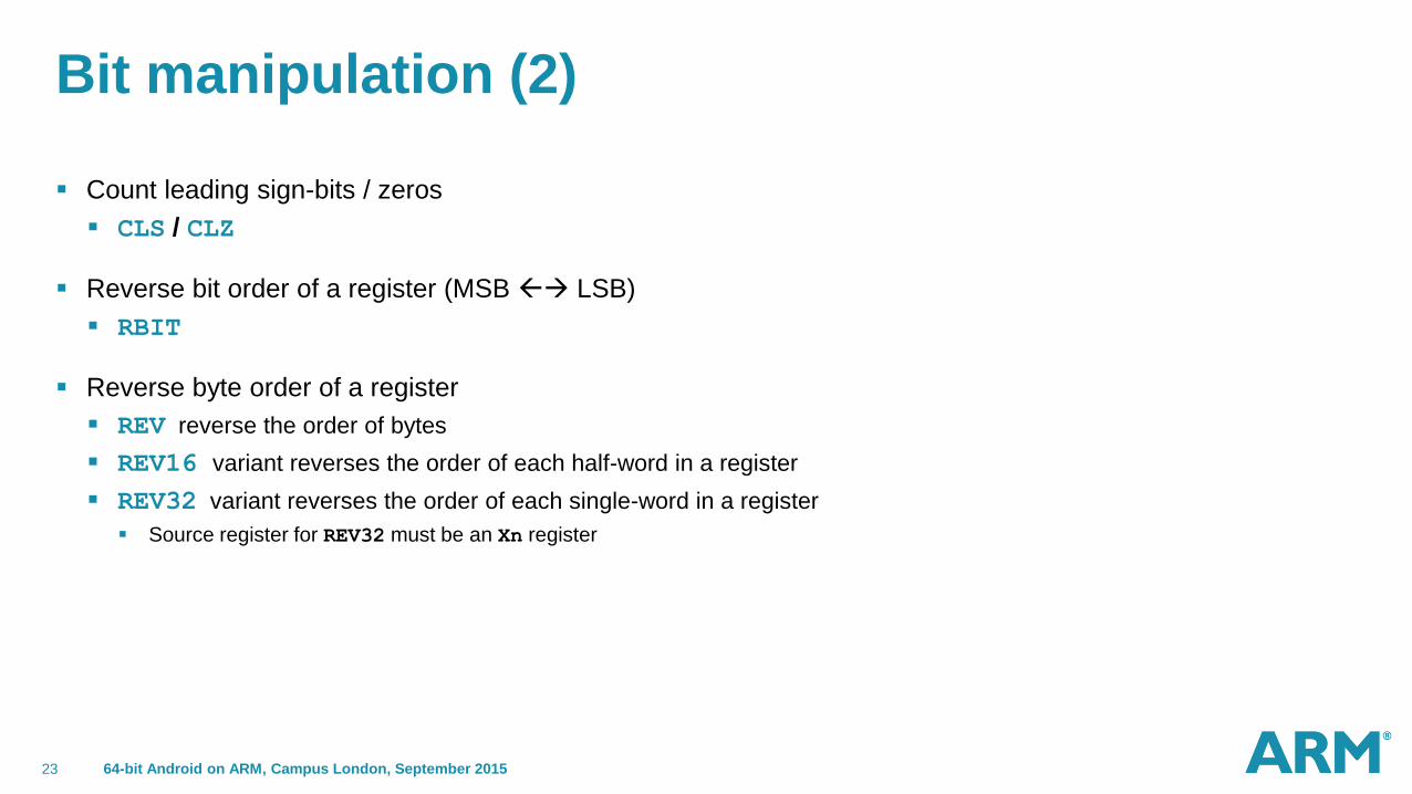
Bit manipulation (2)
Count leading sign-bits / zeros
CLS / CLZ
Reverse bit order of a register (MSB LSB)
RBIT
Reverse byte order of a register
REV reverse the order of bytes
REV16 variant reverses the order of each half-word in a register
REV32 variant reverses the order of each single-word in a register
Source register for REV32 must be an Xn register
64-bit Android on ARM, Campus London, September 20150839 rev 12368 24
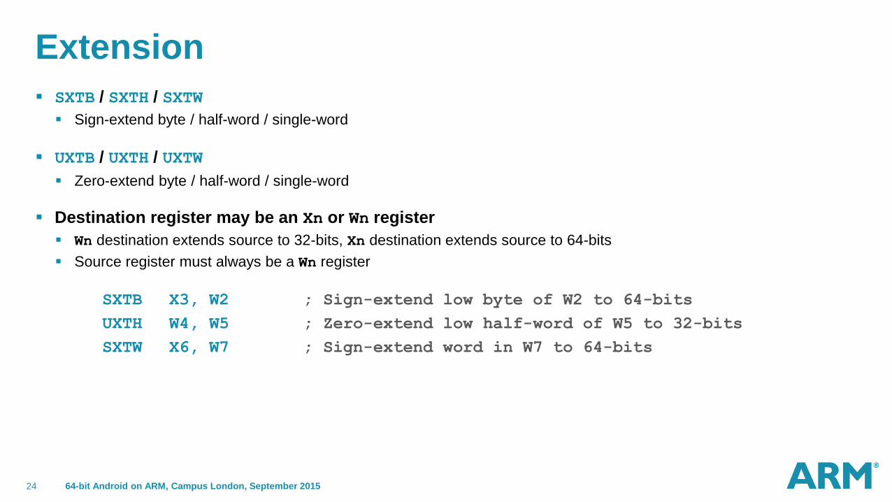
Extension
SXTB / SXTH / SXTW
Sign-extend byte / half-word / single-word
UXTB / UXTH / UXTW
Zero-extend byte / half-word / single-word
Destination register may be an Xn or Wn register
Wn destination extends source to 32-bits, Xn destination extends source to 64-bits
Source register must always be a Wn register
SXTB X3, W2 ; Sign-extend low byte of W2 to 64-bits
UXTH W4, W5 ; Zero-extend low half-word of W5 to 32-bits
SXTW X6, W7 ; Sign-extend word in W7 to 64-bits
64-bit Android on ARM, Campus London, September 20150839 rev 12368 25
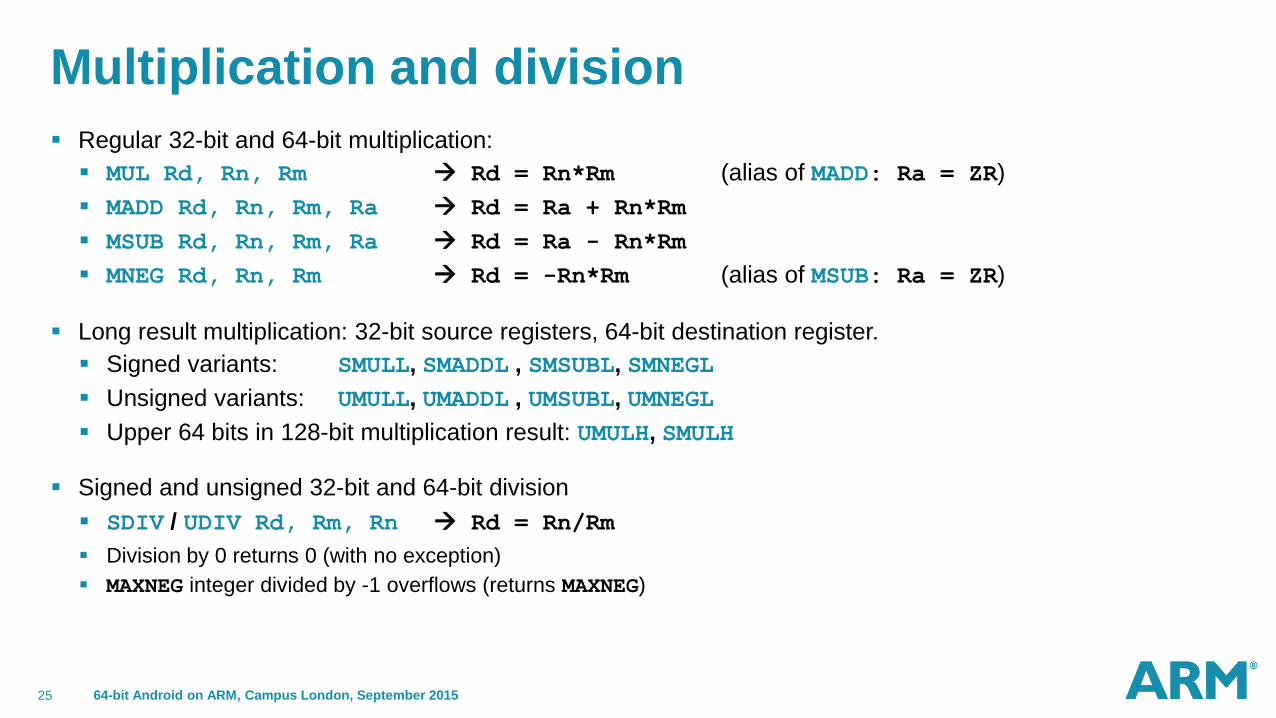
Multiplication and division
Regular 32-bit and 64-bit multiplication:
MUL Rd, Rn, Rm Rd = Rn*Rm (alias of MADD: Ra = ZR)
MADD Rd, Rn, Rm, Ra Rd = Ra + Rn*Rm
MSUB Rd, Rn, Rm, Ra Rd = Ra - Rn*Rm
MNEG Rd, Rn, Rm Rd = -Rn*Rm (alias of MSUB: Ra = ZR)
Long result multiplication: 32-bit source registers, 64-bit destination register.
Signed variants: SMULL, SMADDL , SMSUBL, SMNEGL
Unsigned variants: UMULL, UMADDL , UMSUBL, UMNEGL
Upper 64 bits in 128-bit multiplication result: UMULH, SMULH
Signed and unsigned 32-bit and 64-bit division
SDIV / UDIV Rd, Rm, Rn Rd = Rn/Rm
Division by 0 returns 0 (with no exception)
MAXNEG integer divided by -1 overflows (returns MAXNEG)
64-bit Android on ARM, Campus London, September 20150839 rev 12368 26
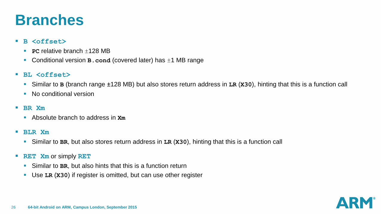
Branches
B <offset>
PC relative branch ±128 MB
Conditional version B.cond (covered later) has ±1 MB range
BL <offset>
Similar to B (branch range ±128 MB) but also stores return address in LR (X30), hinting that this is a function call
No conditional version
BR Xm
Absolute branch to address in Xm
BLR Xm
Similar to BR, but also stores return address in LR (X30), hinting that this is a function call
RET Xm or simply RET
Similar to BR, but also hints that this is a function return
Use LR (X30) if register is omitted, but can use other register
64-bit Android on ARM, Campus London, September 20150839 rev 12368 27
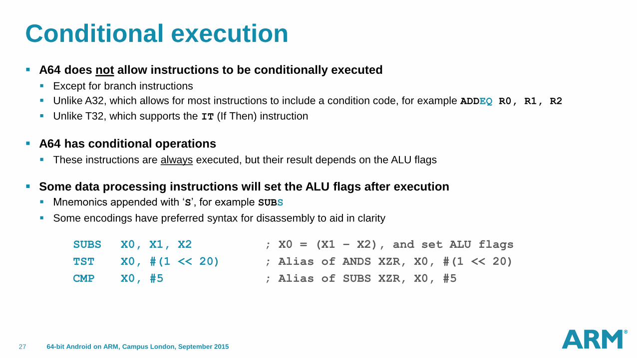
Conditional execution
A64 does not allow instructions to be conditionally executed
Except for branch instructions
Unlike A32, which allows for most instructions to include a condition code, for example ADDEQ R0, R1, R2
Unlike T32, which supports the IT (If Then) instruction
A64 has conditional operations
These instructions are always executed, but their result depends on the ALU flags
Some data processing instructions will set the ALU flags after execution
Mnemonics appended with ‘S’, for example SUBS
Some encodings have preferred syntax for disassembly to aid in clarity
SUBS X0, X1, X2 ; X0 = (X1 – X2), and set ALU flags
TST X0, #(1 << 20) ; Alias of ANDS XZR, X0, #(1 << 20)
CMP X0, #5 ; Alias of SUBS XZR, X0, #5
64-bit Android on ARM, Campus London, September 20150839 rev 12368 28
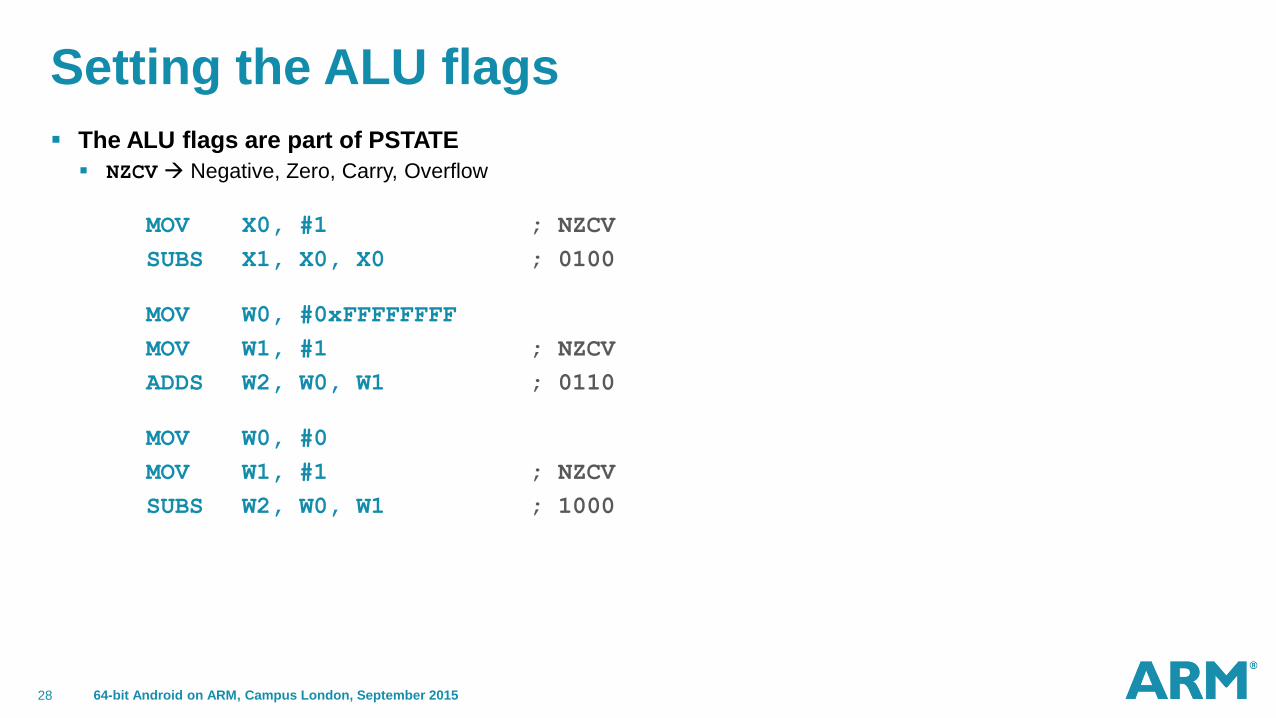
Setting the ALU flags
The ALU flags are part of PSTATE
NZCV Negative, Zero, Carry, Overflow
MOV X0, #1 ; NZCV
SUBS X1, X0, X0 ; 0100
MOV W0, #0xFFFFFFFF
MOV W1, #1 ; NZCV
ADDS W2, W0, W1 ; 0110
MOV W0, #0
MOV W1, #1 ; NZCV
SUBS W2, W0, W1 ; 1000
64-bit Android on ARM, Campus London, September 20150839 rev 12368 29
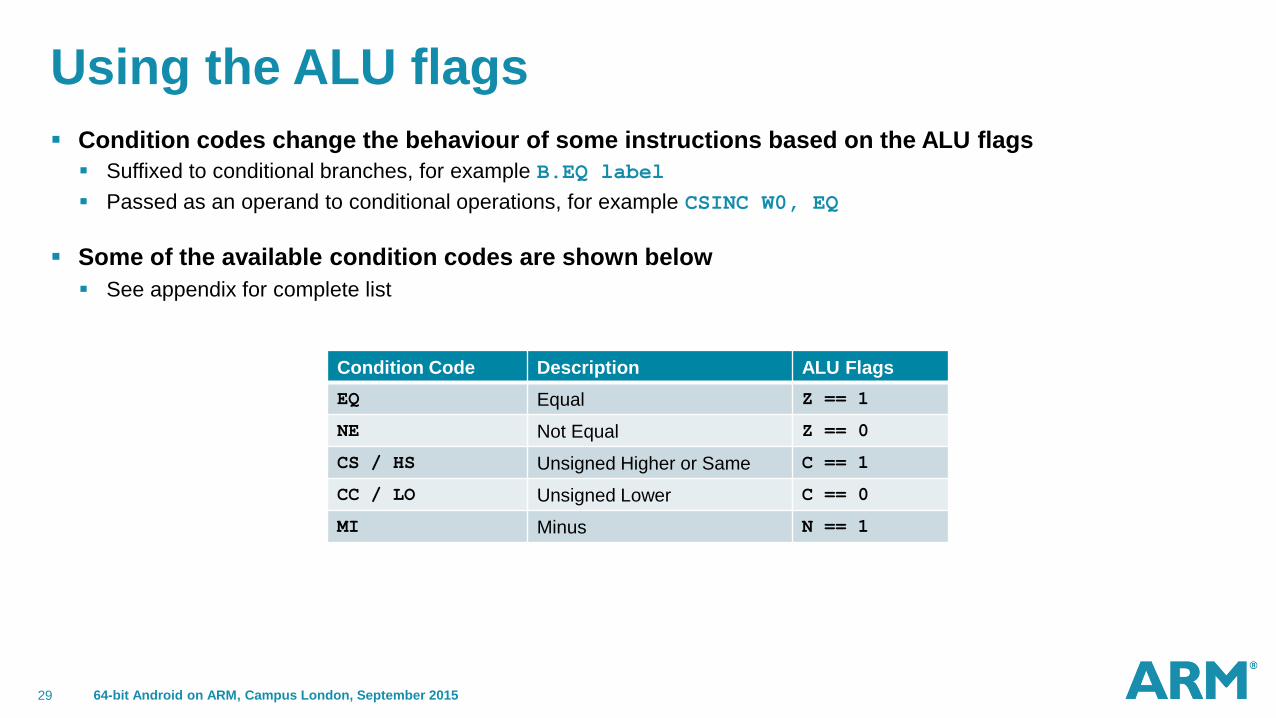
Using the ALU flags
Condition codes change the behaviour of some instructions based on the ALU flags
Suffixed to conditional branches, for example B.EQ label
Passed as an operand to conditional operations, for example CSINC W0, EQ
Some of the available condition codes are shown below
See appendix for complete list
Condition Code Description ALU Flags
EQ Equal Z == 1
NE Not Equal Z == 0
CS / HS Unsigned Higher or Same C == 1
CC / LO Unsigned Lower C == 0
MI Minus N == 1
64-bit Android on ARM, Campus London, September 20150839 rev 12368 30
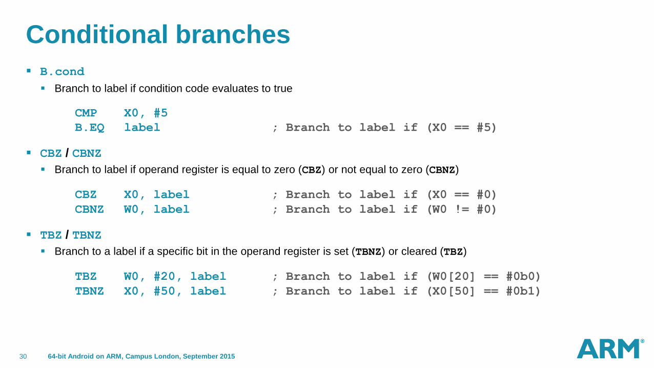
Conditional branches
B.cond
Branch to label if condition code evaluates to true
CMP X0, #5
B.EQ label ; Branch to label if (X0 == #5)
CBZ / CBNZ
Branch to label if operand register is equal to zero (CBZ) or not equal to zero (CBNZ)
CBZ X0, label ; Branch to label if (X0 == #0)
CBNZ W0, label ; Branch to label if (W0 != #0)
TBZ / TBNZ
Branch to a label if a specific bit in the operand register is set (TBNZ) or cleared (TBZ)
TBZ W0, #20, label ; Branch to label if (W0[20] == #0b0)
TBNZ X0, #50, label ; Branch to label if (X0[50] == #0b1)
64-bit Android on ARM, Campus London, September 20150839 rev 12368 31
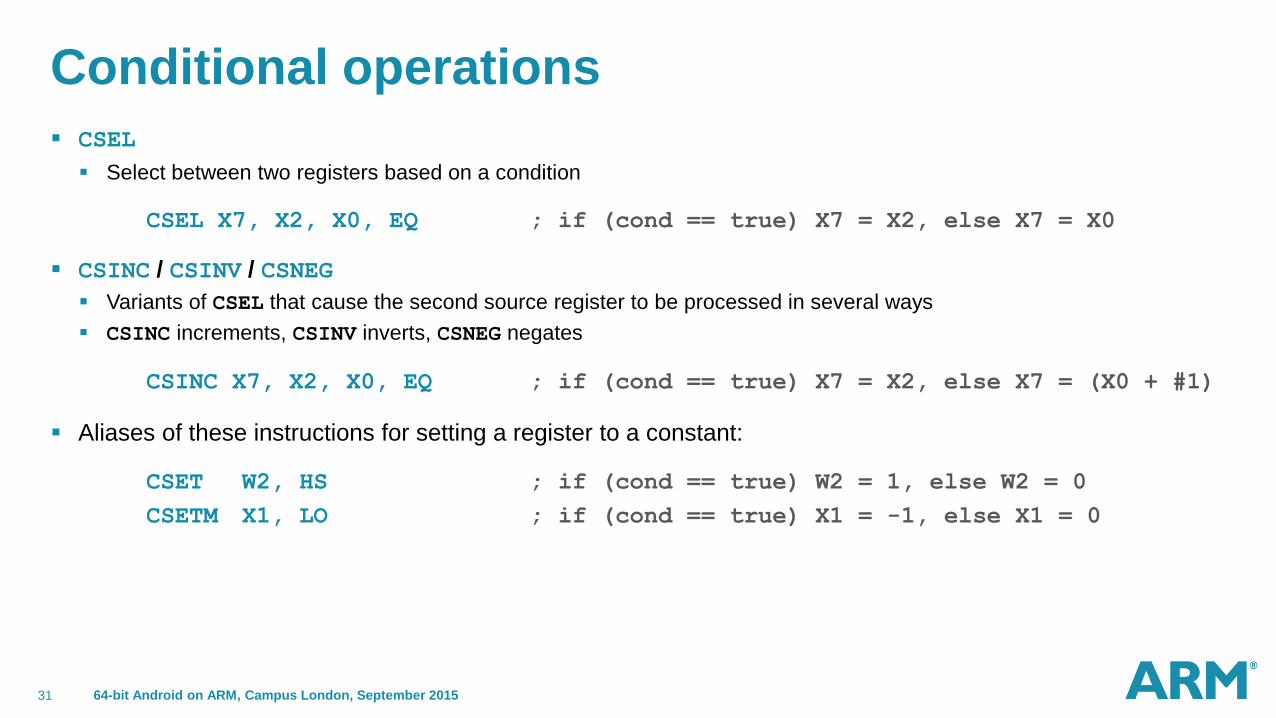
Conditional operations
CSEL
Select between two registers based on a condition
CSEL X7, X2, X0, EQ ; if (cond == true) X7 = X2, else X7 = X0
CSINC / CSINV / CSNEG
Variants of CSEL that cause the second source register to be processed in several ways
CSINC increments, CSINV inverts, CSNEG negates
CSINC X7, X2, X0, EQ ; if (cond == true) X7 = X2, else X7 = (X0 + #1)
Aliases of these instructions for setting a register to a constant:
CSET W2, HS ; if (cond == true) W2 = 1, else W2 = 0
CSETM X1, LO ; if (cond == true) X1 = -1, else X1 = 0
64-bit Android on ARM, Campus London, September 20150839 rev 12368 32
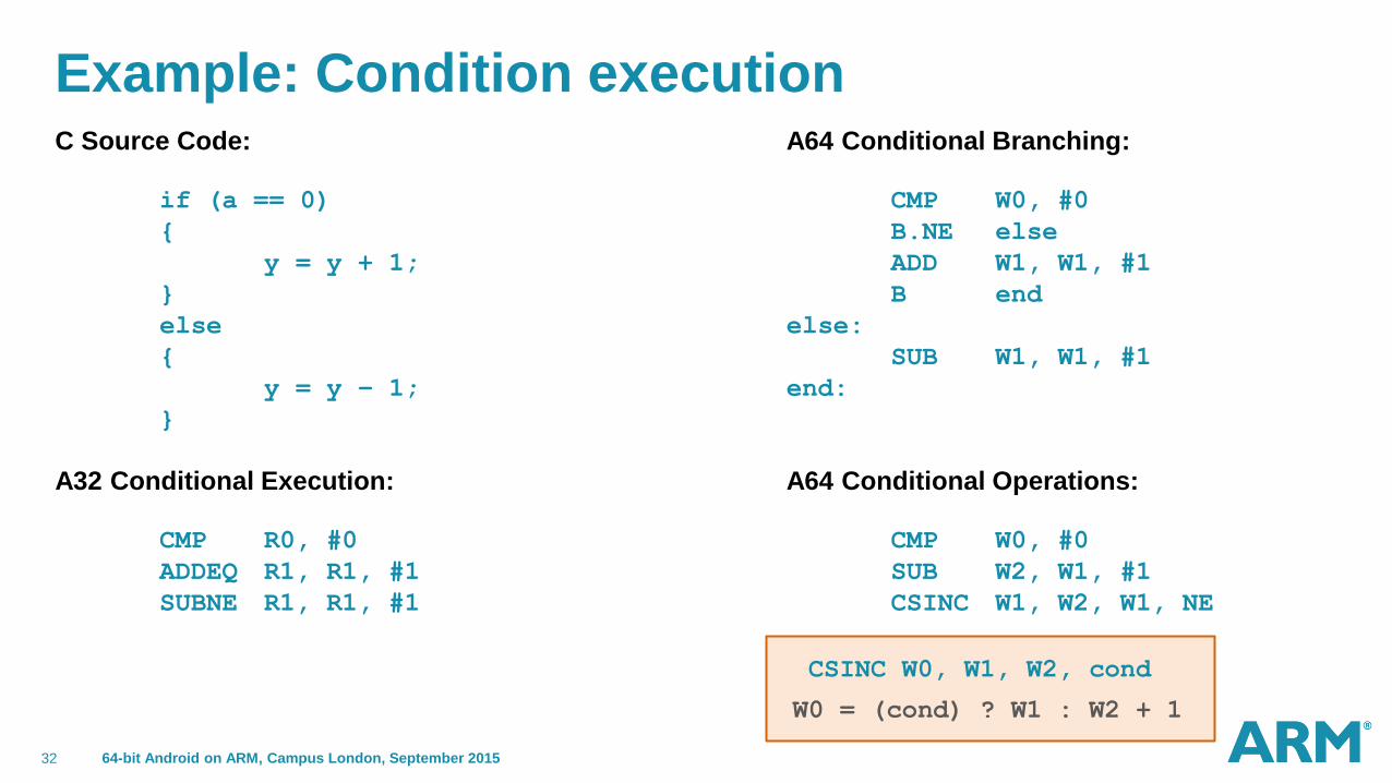
Example: Condition execution C Source Code: A64 Conditional Branching:
if (a == 0) CMP W0, #0
{ B.NE else
y = y + 1; ADD W1, W1, #1
} B end
else else:
{ SUB W1, W1, #1
y = y – 1; end:
}
A32 Conditional Execution: A64 Conditional Operations:
CMP R0, #0 CMP W0, #0
ADDEQ R1, R1, #1 SUB W2, W1, #1
SUBNE R1, R1, #1 CSINC W1, W2, W1, NE
CSINC W0, W1, W2, cond
W0 = (cond) ? W1 : W2 + 1

64-bit Android on ARM, Campus London, September 20150839 rev 12368 33
Agenda
Introduction
Registers
Loads and stores
Data processing and control flow
Scalar floating-point and SIMD
64-bit Android on ARM, Campus London, September 20150839 rev 12368 34
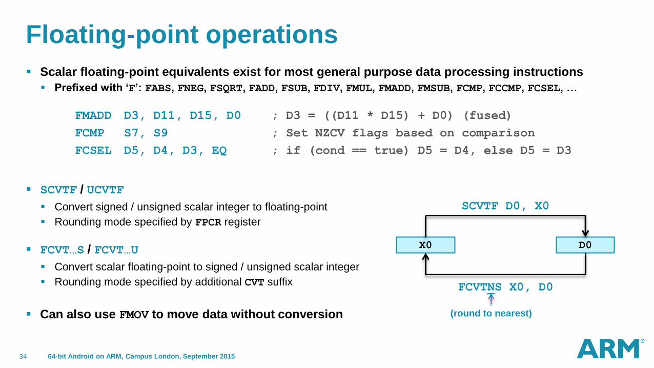
Floating-point operations
Scalar floating-point equivalents exist for most general purpose data processing instructions
Prefixed with ‘F’: FABS, FNEG, FSQRT, FADD, FSUB, FDIV, FMUL, FMADD, FMSUB, FCMP, FCCMP, FCSEL, …
FMADD D3, D11, D15, D0 ; D3 = ((D11 * D15) + D0) (fused)
FCMP S7, S9 ; Set NZCV flags based on comparison
FCSEL D5, D4, D3, EQ ; if (cond == true) D5 = D4, else D5 = D3
SCVTF / UCVTF
Convert signed / unsigned scalar integer to floating-point
Rounding mode specified by FPCR register
FCVT…S / FCVT…U
Convert scalar floating-point to signed / unsigned scalar integer
Rounding mode specified by additional CVT suffix
Can also use FMOV to move data without conversion
X0 D0
SCVTF D0, X0
FCVTNS X0, D0
(round to nearest)
64-bit Android on ARM, Campus London, September 20150839 rev 12368 35
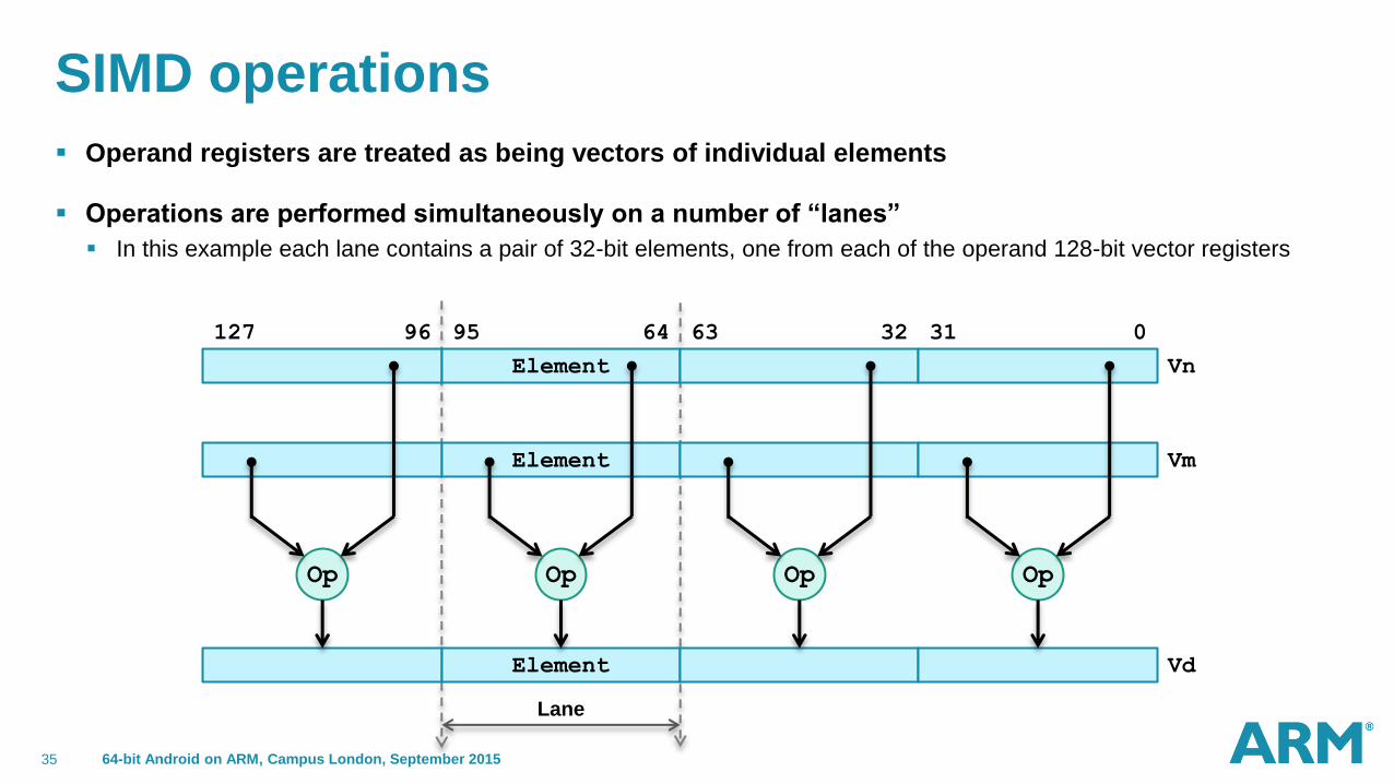
SIMD operations
Operand registers are treated as being vectors of individual elements
Operations are performed simultaneously on a number of “lanes”
In this example each lane contains a pair of 32-bit elements, one from each of the operand 128-bit vector registers
Element
Element
Op
Element
Op Op Op
Vn
Vm
Vd
0 31 32 63 64 95 96 127
Lane

64-bit Android on ARM, Campus London, September 20150839 rev 12368 36
Vectors
When accessing a SIMD vector, the Vn register name is used, with an extension to indicate the
number and size of elements in the vector
Vn.xy
n is the register number, x is the number of elements, y is the size of the elements encoded as a letter
FADD V0.2D, V5.2D, V6.2D ; 2x double-precision floats
Total vector length must be either 128-bits or 64-bits
If 64-bits are written, Vn[127:64] are automatically cleared to 0
ADD V0.8H, V3.8H, V4.8H ; 8x 16-bit integers
ADD V0.8B, V3.8B, V4.8B ; 8x 8-bit integers, clear top of V0
Some instructions refer to a single element of a vector
Example: V3.B[3] – Byte in V3[23:16]
Rest of register is unaffected when an element is written
FMUL V0.4S, V2.4S, V3.S[2] ; Multiply each element of V2 by V3.S[2]
64-bit Android on ARM, Campus London, September 20150839 rev 12368 37
ARMv8-A A64 ISA Overview

64-bit Android on ARM, Campus London, September 20150839 rev 12368 38
Appendix
64-bit Android on ARM, Campus London, September 20150839 rev 12368 39
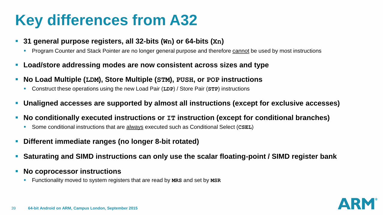
Key differences from A32
31 general purpose registers, all 32-bits (Wn) or 64-bits (Xn)
Program Counter and Stack Pointer are no longer general purpose and therefore cannot be used by most instructions
Load/store addressing modes are now consistent across sizes and type
No Load Multiple (LDM), Store Multiple (STM), PUSH, or POP instructions
Construct these operations using the new Load Pair (LDP) / Store Pair (STP) instructions
Unaligned accesses are supported by almost all instructions (except for exclusive accesses)
No conditionally executed instructions or IT instruction (except for conditional branches)
Some conditional instructions that are always executed such as Conditional Select (CSEL)
Different immediate ranges (no longer 8-bit rotated)
Saturating and SIMD instructions can only use the scalar floating-point / SIMD register bank
No coprocessor instructions Functionality moved to system registers that are read by MRS and set by MSR
64-bit Android on ARM, Campus London, September 20150839 rev 12368 40
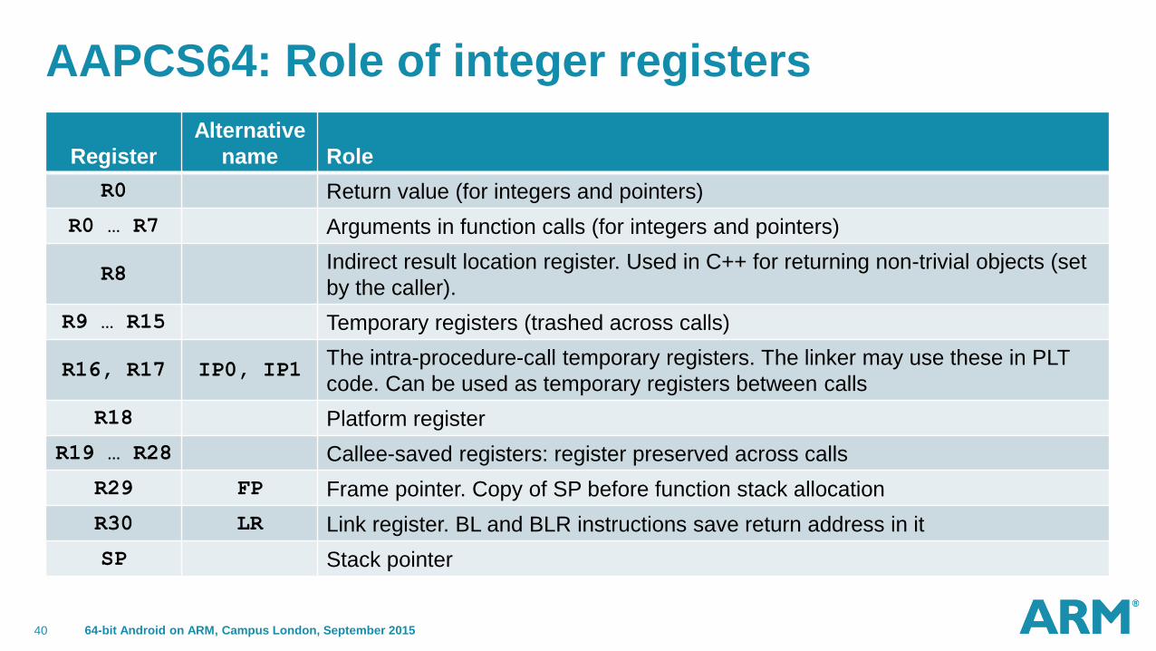
AAPCS64: Role of integer registers
Register
Alternative
name Role
R0 Return value (for integers and pointers)
R0 … R7 Arguments in function calls (for integers and pointers)
R8 Indirect result location register. Used in C++ for returning non-trivial objects (set
by the caller).
R9 … R15 Temporary registers (trashed across calls)
R16, R17 IP0, IP1 The intra-procedure-call temporary registers. The linker may use these in PLT
code. Can be used as temporary registers between calls
R18 Platform register
R19 … R28 Callee-saved registers: register preserved across calls
R29 FP Frame pointer. Copy of SP before function stack allocation
R30 LR Link register. BL and BLR instructions save return address in it
SP Stack pointer
64-bit Android on ARM, Campus London, September 20150839 rev 12368 41
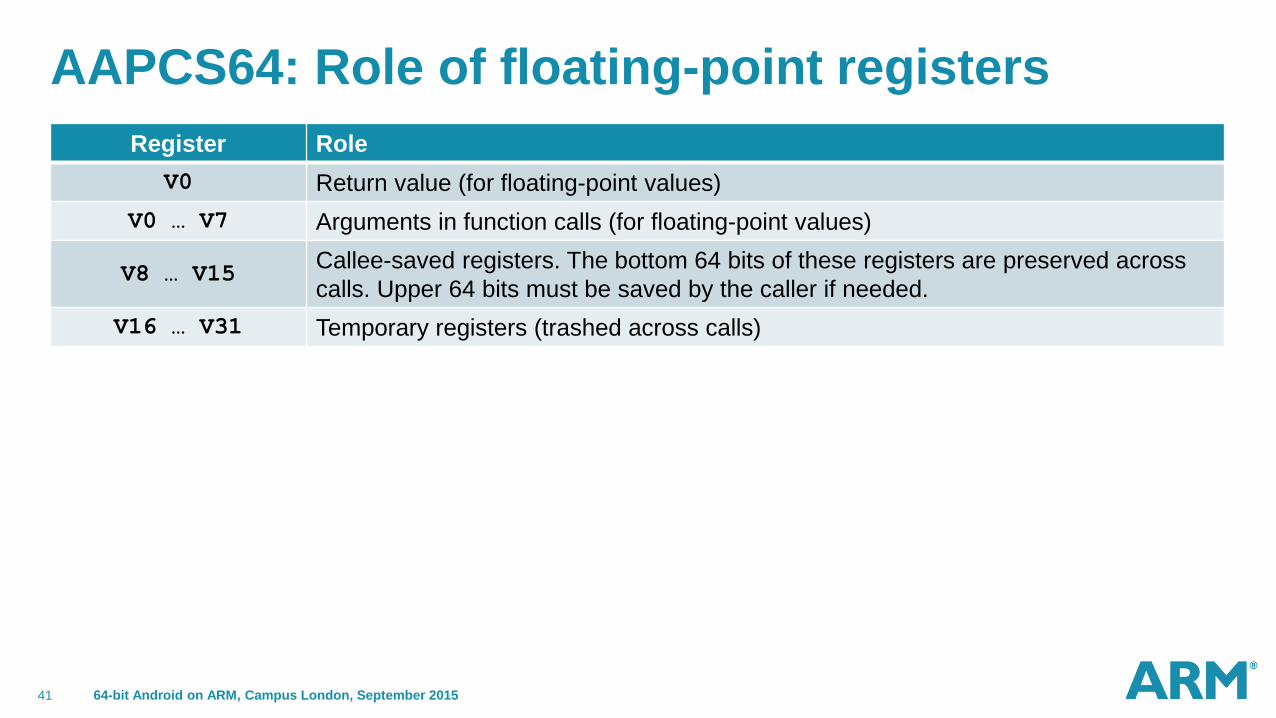
AAPCS64: Role of floating-point registers
Register Role
V0 Return value (for floating-point values)
V0 … V7 Arguments in function calls (for floating-point values)
V8 … V15 Callee-saved registers. The bottom 64 bits of these registers are preserved across
calls. Upper 64 bits must be saved by the caller if needed.
V16 … V31 Temporary registers (trashed across calls)

64-bit Android on ARM, Campus London, September 20150839 rev 12368 42
Specifying register load size
Load Size Extension Xn Wn
8-bit Zero -- LDRB
Sign LDRSB LDRSB
16-bit Zero -- LDRH
Sign LDRSH LDRSH
32-bit Zero -- LDR
Sign LDRSW --
64-bit Zero LDR --
There is no encoding for a zero-extended load of less than 64-bits to an Xn register
Writing to a Wn register automatically clears bits [63:32], which accomplishes the same thing
Store Size Xn Wn
8-bit -- STRB
16-bit -- STRH
32-bit -- STR
64-bit STR --
64-bit Android on ARM, Campus London, September 20150839 rev 12368 43
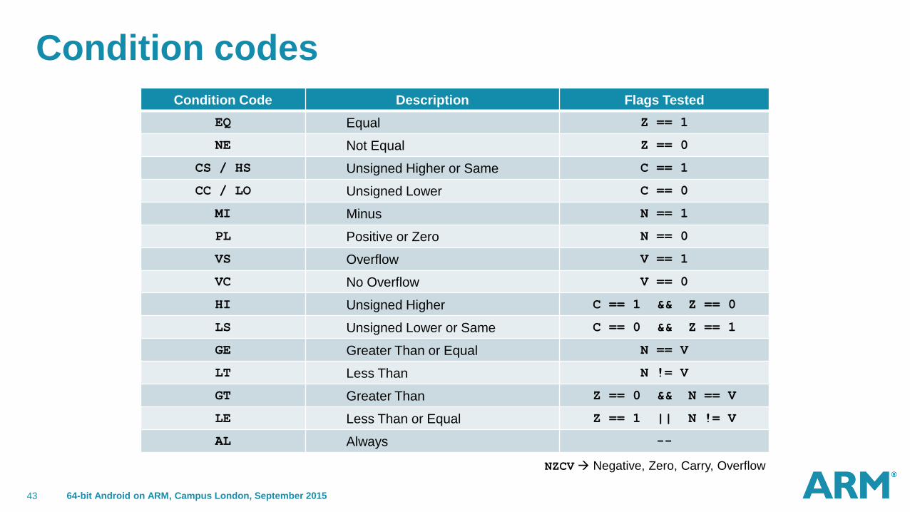
Condition codes
Condition Code Description Flags Tested
EQ Equal Z == 1
NE Not Equal Z == 0
CS / HS Unsigned Higher or Same C == 1
CC / LO Unsigned Lower C == 0
MI Minus N == 1
PL Positive or Zero N == 0
VS Overflow V == 1
VC No Overflow V == 0
HI Unsigned Higher C == 1 && Z == 0
LS Unsigned Lower or Same C == 0 && Z == 1
GE Greater Than or Equal N == V
LT Less Than N != V
GT Greater Than Z == 0 && N == V
LE Less Than or Equal Z == 1 || N != V
AL Always --
NZCV Negative, Zero, Carry, Overflow
64-bit Android on ARM, Campus London, September 20150839 rev 12368 44
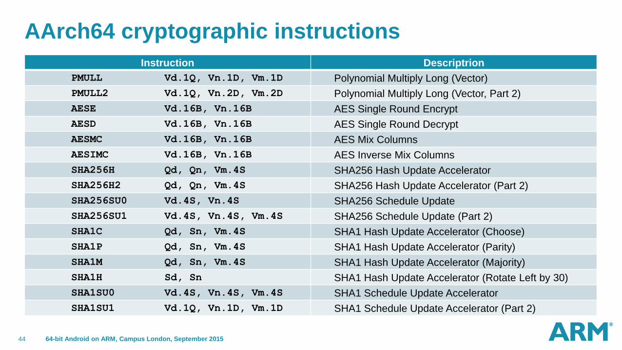
AArch64 cryptographic instructions
Instruction Descriptrion
PMULL Vd.1Q, Vn.1D, Vm.1D Polynomial Multiply Long (Vector)
PMULL2 Vd.1Q, Vn.2D, Vm.2D Polynomial Multiply Long (Vector, Part 2)
AESE Vd.16B, Vn.16B AES Single Round Encrypt
AESD Vd.16B, Vn.16B AES Single Round Decrypt
AESMC Vd.16B, Vn.16B AES Mix Columns
AESIMC Vd.16B, Vn.16B AES Inverse Mix Columns
SHA256H Qd, Qn, Vm.4S SHA256 Hash Update Accelerator
SHA256H2 Qd, Qn, Vm.4S SHA256 Hash Update Accelerator (Part 2)
SHA256SU0 Vd.4S, Vn.4S SHA256 Schedule Update
SHA256SU1 Vd.4S, Vn.4S, Vm.4S SHA256 Schedule Update (Part 2)
SHA1C Qd, Sn, Vm.4S SHA1 Hash Update Accelerator (Choose)
SHA1P Qd, Sn, Vm.4S SHA1 Hash Update Accelerator (Parity)
SHA1M Qd, Sn, Vm.4S SHA1 Hash Update Accelerator (Majority)
SHA1H Sd, Sn SHA1 Hash Update Accelerator (Rotate Left by 30)
SHA1SU0 Vd.4S, Vn.4S, Vm.4S SHA1 Schedule Update Accelerator
SHA1SU1 Vd.1Q, Vn.1D, Vm.1D SHA1 Schedule Update Accelerator (Part 2)