arm corelink mmu-500 system memory management unit...
TRANSCRIPT

ARM® CoreLink™ MMU-500 SystemMemory Management Unit
Revision: r2p4
Technical Reference Manual
Copyright © 2013, 2014, 2016 ARM. All rights reserved.ARM DDI 0517F (ID041216)

ARM CoreLink MMU-500 System Memory Management UnitTechnical Reference Manual
Copyright © 2013, 2014, 2016 ARM. All rights reserved.
Release Information
The following changes have been made to this book.
Proprietary Notice
This document is protected by copyright and other related rights and the practice or implementation of the information contained in this document may be protected by one or more patents or pending patent applications. No part of this document may be reproduced in any form by any means without the express prior written permission of ARM. No license, express or implied, by estoppel or otherwise to any intellectual property rights is granted by this document unless specifically stated.
Your access to the information in this document is conditional upon your acceptance that you will not use or permit others to use the information for the purposes of determining whether implementations infringe any third party patents.
THIS DOCUMENT IS PROVIDED “AS IS”. ARM PROVIDES NO REPRESENTATIONS AND NO WARRANTIES, EXPRESS, IMPLIED OR STATUTORY, INCLUDING, WITHOUT LIMITATION, THE IMPLIED WARRANTIES OF MERCHANTABILITY, SATISFACTORY QUALITY, NON-INFRINGEMENT OR FITNESS FOR A PARTICULAR PURPOSE WITH RESPECT TO THE DOCUMENT. For the avoidance of doubt, ARM makes no representation with respect to, and has undertaken no analysis to identify or understand the scope and content of, third party patents, copyrights, trade secrets, or other rights.
This document may include technical inaccuracies or typographical errors.
TO THE EXTENT NOT PROHIBITED BY LAW, IN NO EVENT WILL ARM BE LIABLE FOR ANY DAMAGES, INCLUDING WITHOUT LIMITATION ANY DIRECT, INDIRECT, SPECIAL, INCIDENTAL, PUNITIVE, OR CONSEQUENTIAL DAMAGES, HOWEVER CAUSED AND REGARDLESS OF THE THEORY OF LIABILITY, ARISING OUT OF ANY USE OF THIS DOCUMENT, EVEN IF ARM HAS BEEN ADVISED OF THE POSSIBILITY OF SUCH DAMAGES.
This document consists solely of commercial items. You shall be responsible for ensuring that any use, duplication or disclosure of this document complies fully with any relevant export laws and regulations to assure that this document or any portion thereof is not exported, directly or indirectly, in violation of such export laws. Use of the word “partner” in reference to ARM’s customers is not intended to create or refer to any partnership relationship with any other company. ARM may make changes to this document at any time and without notice.
If any of the provisions contained in these terms conflict with any of the provisions of any signed written agreement covering this document with ARM, then the signed written agreement prevails over and supersedes the conflicting provisions of these terms.
Words and logos marked with ® or ™ are registered trademarks or trademarks of ARM Limited or its affiliates in the EU and/or elsewhere. All rights reserved. Other brands and names mentioned in this document may be the trademarks of their respective owners. Please follow ARM’s trademark usage guidelines at http://www.arm.com/about/trademarks/guidelines/index.php
Copyright © 2013, 2014, 2016 ARM Limited or its affiliates. All rights reserved.
ARM Limited. Company 02557590 registered in England.
Change history
Date Issue Confidentiality Change
22 August 2013 A Non-Confidential First release for r0p0.
28 November 2013 B Non-Confidential First release for r1p0.
25 February 2014 C Non-Confidential First release for r2p0.
03 June 2014 D Non-Confidential First release for r2p1.
28 November 2014 E Non-Confidential First release for r2p2.
12 February 2016 F Non-Confidential First release for r2p4.
ARM DDI 0517F Copyright © 2013, 2014, 2016 ARM. All rights reserved. iiID041216 Non-Confidential

110 Fulbourn Road, Cambridge, England CB1 9NJ.
LES-PRE-20349
Confidentiality Status
This document is Non-Confidential. The right to use, copy and disclose this document may be subject to license restrictions in accordance with the terms of the agreement entered into by ARM and the party that ARM delivered this document to.
Product Status
The information in this document is final, that is for a developed product.
Web Address
http://www.arm.com
ARM DDI 0517F Copyright © 2013, 2014, 2016 ARM. All rights reserved. iiiID041216 Non-Confidential

ContentsARM CoreLink MMU-500 System Memory Management Unit Technical Reference Manual
PrefaceAbout this book .......................................................................................................... viiFeedback ..................................................................................................................... x
Chapter 1 Introduction1.1 About the MMU-500 ................................................................................................. 1-21.2 Compliance .............................................................................................................. 1-61.3 Features ................................................................................................................... 1-71.4 Interfaces ................................................................................................................. 1-91.5 Configurable options ............................................................................................. 1-101.6 Product documentation and design flow ................................................................ 1-121.7 Test features .......................................................................................................... 1-141.8 Product revisions ................................................................................................... 1-15
Chapter 2 Functional description2.1 About the functions .................................................................................................. 2-22.2 Interfaces ................................................................................................................. 2-42.3 Operation ............................................................................................................... 2-122.4 Cache structures of the MMU-500 ......................................................................... 2-192.5 Constraints and limitations of use .......................................................................... 2-21
Chapter 3 Programmers model3.1 About this programmers model ................................................................................ 3-23.2 Modes of operation and execution ........................................................................... 3-33.3 Memory model ......................................................................................................... 3-43.4 Register summary .................................................................................................... 3-9
ARM DDI 0517F Copyright © 2013, 2014, 2016 ARM. All rights reserved. ivID041216 Non-Confidential

3.5 Global address space 0 ......................................................................................... 3-123.6 Global address space 1 ......................................................................................... 3-243.7 Translation context address space ........................................................................ 3-253.8 Integration registers ............................................................................................... 3-263.9 Peripheral and component identification registers ................................................. 3-36
Appendix A Signal descriptionsA.1 Clock and reset signals ............................................................................................ A-2A.2 ACE-Lite signals ...................................................................................................... A-3A.3 Low-power interface signals .................................................................................. A-11A.4 Miscellaneous signals ............................................................................................ A-13
Appendix B Revisions
ARM DDI 0517F Copyright © 2013, 2014, 2016 ARM. All rights reserved. vID041216 Non-Confidential

Preface
This preface introduces the ARM® Corelink™ MMU-500 System Memory Management Unit Technical Reference Manual. It contains the following sections:• About this book on page vii.• Feedback on page x.
ARM DDI 0517F Copyright © 2013, 2014, 2016 ARM. All rights reserved. viID041216 Non-Confidential

Preface
About this bookThis book is for the MMU-500.
Product revision status
The rnpn identifier indicates the revision status of the product described in this book, where:rn Identifies the major revision of the product.pn Identifies the minor revision or modification status of the product.
Intended audience
This book is written for system designers, system integrators, and programmers who are designing or programming a device that uses the MMU-500.
Using this book
This book is organized into the following chapters:
Chapter 1 Introduction Read this for an introduction to the MMU-500 and its features.
Chapter 2 Functional description Read this for an overview of the major functional blocks and the operation of the MMU-500.
Chapter 3 Programmers model Read this for a description of the MMU-500 memory map and registers.
Appendix A Signal descriptions Read this for a description of the MMU-500 signals.
Appendix B Revisions Read this for a description of the technical changes between released issues of this book.
Glossary
The ARM® Glossary is a list of terms used in ARM documentation, together with definitions for those terms. The ARM® Glossary does not contain terms that are industry standard unless the ARM meaning differs from the generally accepted meaning.
See ARM® Glossary, http://infocenter.arm.com/help/topic/com.arm.doc.aeg0014-/index.html.
Conventions
This book uses the conventions that are described in:• Typographical conventions on page viii.• Signals on page viii.
ARM DDI 0517F Copyright © 2013, 2014, 2016 ARM. All rights reserved. viiID041216 Non-Confidential

Preface
Typographical conventions
The following table describes the typographical conventions:
Signals
The signal conventions are:
Signal level The level of an asserted signal depends on whether the signal is active-HIGH or active-LOW. Asserted means:• HIGH for active-HIGH signals.• LOW for active-LOW signals.
Lowercase n At the start or end of a signal name denotes an active-LOW signal.
Additional reading
This section lists publications by ARM and by third parties.
See Infocenter, http://infocenter.arm.com, for access to ARM documentation.
ARM publications
This book contains information that is specific to this product. See the following documents for other relevant information:
• ARM® System Memory Management Unit Architecture Specification (ARM IHI 0062).
• ARM® CoreSight™ Architecture Specification (ARM IHI 0029).
• ARM® Architecture Reference Manual ARMv7-A and ARMv7-R edition (ARM DDI 0406).
• ARM® Architecture Reference Manual, ARMv8, for ARMv8-A architecture profile (ARM DDI 0487).
• ARM® AMBA® AXI and ACE Protocol Specification AXI3, AXI4, and AXI4-Lite ACE and ACE-Lite (ARM IHI 0022).
Typographical conventions
Style Purpose
italic Introduces special terminology, denotes cross-references, and citations.
bold Highlights interface elements, such as menu names. Denotes signal names. Also used for terms in descriptive lists, where appropriate.
monospace Denotes text that you can enter at the keyboard, such as commands, file and program names, and source code.
monospace Denotes a permitted abbreviation for a command or option. You can enter the underlined text instead of the full command or option name.
monospace italic Denotes arguments to monospace text where the argument is to be replaced by a specific value.
monospace bold Denotes language keywords when used outside example code.
<and> Encloses replaceable terms for assembler syntax where they appear in code or code fragments. For example:MRC p15, 0 <Rd>, <CRn>, <CRm>, <Opcode_2>
SMALL CAPITALS Used in body text for a few terms that have specific technical meanings, that are defined in the ARM® Glossary. For example, IMPLEMENTATION DEFINED, IMPLEMENTATION SPECIFIC, UNKNOWN, and UNPREDICTABLE.
ARM DDI 0517F Copyright © 2013, 2014, 2016 ARM. All rights reserved. viiiID041216 Non-Confidential

Preface
• Low Power Interface Specification, ARM® Q-Channel and P-Channel Interfaces (ARM IHI 0068).
The following confidential books are only available to licensees:
• ARM® CoreLink™ MMU-500 System Memory Management Unit Supplement to AMBA® Designer (ADR-400) User Guide (ARM DSU 0031).
• ARM® CoreLink™ MMU-500 System Memory Management Unit Technical Reference Manual Supplement (ARM DSU 0030).
• ARM® CoreLink™ MMU-500 System Memory Management Unit Implementation Guide (ARM DII 0289).
• ARM® CoreLink™ MMU-500 System Memory Management Unit Integration Manual (ARM DIT 0051).
ARM DDI 0517F Copyright © 2013, 2014, 2016 ARM. All rights reserved. ixID041216 Non-Confidential

Preface
FeedbackARM welcomes feedback on this product and its documentation.
Feedback on this product
If you have any comments or suggestions about this product, contact your supplier and give:• The product name.• The product revision or version.• An explanation with as much information as you can provide. Include symptoms and
diagnostic procedures if appropriate.
Feedback on content
If you have comments on content then send an e-mail to [email protected]. Give:• The title.• The number, ARM DDI 0517F.• The page numbers to which your comments apply.• A concise explanation of your comments.
ARM also welcomes general suggestions for additions and improvements.
Note ARM tests the PDF only in Adobe Acrobat and Acrobat Reader, and cannot guarantee the quality of the represented document when used with any other PDF reader.
ARM DDI 0517F Copyright © 2013, 2014, 2016 ARM. All rights reserved. xID041216 Non-Confidential

Chapter 1 Introduction
This chapter provides an overview of the MMU-500. It contains the following sections:• About the MMU-500 on page 1-2.• Compliance on page 1-6.• Features on page 1-7.• Interfaces on page 1-9.• Configurable options on page 1-10.• Product documentation and design flow on page 1-12.• Test features on page 1-14.• Product revisions on page 1-15.
ARM DDI 0517F Copyright © 2013, 2014, 2016 ARM. All rights reserved. 1-1ID041216 Non-Confidential

Introduction
1.1 About the MMU-500The MMU-500 is a system-level Memory Management Unit (MMU) that translates an input address to an output address, based on address mapping and memory attribute information available in the MMU-500 internal registers and translation tables.
An address translation from an input address to an output address is described as a stage of address translation.
The MMU-500 supports the translation table formats defined by the ARM architecture, ARMv7 and ARMv8, and can perform:
• Stage 1 translations that translate an input Virtual Address (VA) to an output Physical Address (PA) or Intermediate Physical Address (IPA).
• Stage 2 translations that translate an input IPA to an output PA.
• Combined stage 1 and stage 2 translations that translate an input VA to an output IPA, and then translate that IPA to a PA. The MMU-500 performs translation table walks for each stage of the translation.
Address translation can span over two stages, namely stage 1 and stage 2. Address translation can require multiple translation table lookups. Each translation table lookup is described as a level of address lookup. Each level of stage 1 translation might require additional stage 2 translation.
In addition to translating an input address to an output address, a stage of address translation also defines the memory attributes of the output address. With a two-stage translation, the stage 2 translation can modify the attributes defined by the stage 1 translation.
A stage of address translation can be disabled or bypassed, and the MMU-500 can define memory attributes for disabled and bypassed stages of translation.
The MMU-500 uses inputs from the requesting master to identify a context. This context tells the MMU-500 what resources to use for the translation, including the translation tables to use.
For the stage 1 translations that are typically associated with application and OS-level operation, the VA range can be split into two subranges, translated by Translation Table Base registers, TTBR0 and TTBR1, each with associated translation tables and control registers.
These features mean the MMU-500 can perform address translations with the following page size limitations, for memory accesses from either AArch32 state or from AArch64 state:
ARMv7 architecture The MMU-500 supports all page sizes.
ARMv8 architecture Apart from the 16KB page granule, the MMU-500 supports all page sizes.
Stage 1 translations are supported for both Secure and Non-secure translation contexts. Usually, the appropriate OS:
• Defines the translation tables, in memory, for the stage 1 translations for its security state.
• Programs the MMU-500 to configure stage 1 translations, and then enables the translations.
ARM DDI 0517F Copyright © 2013, 2014, 2016 ARM. All rights reserved. 1-2ID041216 Non-Confidential

Introduction
Stage 2 translations are supported only for Non-secure translation contexts. The typical usage model for two stages of address translation is as follows:
• The Non-secure operating system defines the stage 1 address translations for application-level and OS-level operation. It does this assuming it is mapping from the VAs used by the processors to PAs in the physical memory system. However, it actually maps VAs to IPAs.
Note This mapping means that all the addresses the OS uses in the translation tables that it
defines are in the IPA address space, and require a stage 2 translation to map them to the PA address space.
• The hypervisor defines the stage 2 address translations that map the IPAs to PAs. It does this as part of its virtualization of one or more Non-secure guest operating systems.
The MMU-500 can cache the result of a translation table lookup in a Translation Lookaside Buffer (TLB) that means the MMU-500 also supports TLB maintenance operations.
For more information about:
• The supported architectural features of the MMU-500, see the ARM® System Memory Management Architecture Specification.
• Address translation, including the translation table formats and TLB maintenance operations, see:
— The ARM® Architecture Reference Manual, ARMv7-A and ARMv-7 R edition.— The ARM® Architecture Reference Manual, ARMv8, for ARMv8-A architecture
profile.
The MMU-500 has the following key components:
Translation Buffer Unit (TBU) The TBU contains a TLB that caches page tables. The MMU-500 implements a TBU for each connected master, and the TBU is designed, so that it is local to the master.
Translation Control Unit (TCU) Controls and manages the address translations. The MMU-500 implements a single TCU.
Interconnect Connects multiple TBUs to the TCU.
Figure 1-1 on page 1-4 shows the MMU-500 block diagram.
ARM DDI 0517F Copyright © 2013, 2014, 2016 ARM. All rights reserved. 1-3ID041216 Non-Confidential

Introduction
Figure 1-1 MMU-500 block diagram
For more information about logical processing steps, interfaces, and operational features, see Chapter 2 Functional description.
The following are example masters for the MMU-500:• Graphics Processor Unit (GPU).• Video engines.• Direct Memory Access (DMA) controllers.• Color LCD (CLCD) controllers.• Network controllers.
1.1.1 MMU-500 example system
Figure 1-2 on page 1-5 shows the MMU-500 in an example ARM processor and CoreLink Cache Coherent Interconnect-400 (CCI-400) system, performing address translation functions for multiple masters including a GPU.
TCUTBU0
TLB Low-power interface for TBU0
ACE-Lite for TBU0
TBU1
TLB
ACE-Litefor TBU1
TBU0 event
ACE-Lite for TBU1
TBU1 event
TBUn
TLB
ACE-Lite for TBUn
ACE-Lite for TBUn
TBUn event
Programming interface
Interconnect
Invalidation +
DVM
Low-power interface
ACE-Lite
Distributed Virtual Memory (DVM)
AXI4 programming interface
Page Table Walk (PTW)
Interrupts
Low-power interface
Low-power interfacefor TBU1
Low-power interfacefor TBUn
ACE-Litefor TBU0
AXI stream interface
ARM DDI 0517F Copyright © 2013, 2014, 2016 ARM. All rights reserved. 1-4ID041216 Non-Confidential

Introduction
In the example system, transactions sent by the GPU master are received by the TBU on its slave interface to search for a TLB hit. On a miss, the TBU interacts with the TCU through its AXI stream interface, and initiates a page table walk. On receiving the page table entry or a TLB hit, the TBU then forwards the transaction to its master interface after the pending translation based on the page entry.
Figure 1-2 MMU-500 in system context
Note If an AXI3 or AXI4 interface is connected to an ACE-Lite port, then the unused ACE-Lite signals must be tied off to the values shown in Table 2-2 on page 2-21.
TBU2
AXI3
Clock and
power bridge
Clock and
power bridge
TBU5
AXI4
AXI4
TBU3
AXI4
AXI4
Clock and
power bridge
Clock and
power bridge
TBU4
AXI3
AXI3
TBU1
Sidebandc
TBU0
Performance event_busc
ACE-Lite
ACE-Lite
CCIb
spniden
arqosarb
cfg_cttw
Programming I/F 64-bit AXI
Interrupts
AXIStream
AXI StreamAXI Stream
AXIStream
PTW
DVM
a. GPU is an example master for the MMU-500.b. CCI-400 is not a part of the MMU-500.c. The sysbardisable_<tbuname> signals, performance event bus, and other sideband signals are present on all TBUs. These are shown on only one TBU for convenience.
ACE-Lite
ACE-Lite
ACE-Lite
Interconnect TCU
integ_sec_override
GPUa
sysbardisable_tbu1c
AXI3
cfg_normalize
ARM DDI 0517F Copyright © 2013, 2014, 2016 ARM. All rights reserved. 1-5ID041216 Non-Confidential

Introduction
1.2 ComplianceThis TRM complements architecture reference manuals, architecture specifications, protocol specifications, and relevant external standards. It does not duplicate information from these sources.
ARM SMMU architecture The MMU-500 implements the ARM SMMU architecture v2.
See the ARM® System Memory Management Unit Architecture Specification.
ARMv7 and v8 architecture The MMU-500 supports the ARMv7 and ARMv8 address translation schemes. That is, it supports VMSAv7, VMSAv8-32, and VMSAv8-64, including the long-descriptor and short-descriptor translation table formats.
Note The 16KB page granule is not supported in the MMU-500.
See the following documents:
• ARM® Architecture Reference Manual, ARMv8, for ARMv8-A architecture profile.
• ARM® Architecture Reference Manual ARMv7-A and ARMv7-R edition.
Low-power interface support For more information about the MMU-500 low-power interface support, see the following documents: • Low Power Interface Specification, ARM® Q-Channel and P-Channel
Interfaces.• ARM® AMBA® AXI and ACE Protocol Specification AXI3, AXI4, and
AXI4-Lite ACE and ACE-Lite.
ARM DDI 0517F Copyright © 2013, 2014, 2016 ARM. All rights reserved. 1-6ID041216 Non-Confidential

Introduction
1.3 FeaturesThe MMU-500 provides the following features:
• Address virtualization to other masters in an ARM processor based system and other bus masters in the system.
• Support for the following translations:— Stage 1.— Stage 2.— Stage 1 followed by stage 2.
• Programmable Quality of Service (QoS).
• Distributed translation support for up to 32 TBUs.
• Translation support for 32-bit to 49-bit virtual address ranges and 48-bit physical address ranges.
• Multiple transaction contexts to apply to address translations for specific streams of transactions.— Supports up to 128 configurable contexts and programmable page size. The
MMU-500 maps each context by using an input stream ID from the master device that requires address translation.
• Translation support for the following:— Stage 1 ARMv7 VMSA.— Stage 1 and Stage 2 ARMv8 AArch32.— Stage 1 and Stage 2 ARMv8 AArch64 with 4KB and 64KB granules.— Stage 1 followed by stage 2 translations.
• No page size restrictions. All page sizes are supported apart from the 16KB page granule defined by ARMv8 architecture.
• Arbitration of PTW requests from different TBUs by using the programmed QoS value.
• Page table walk cache for storing intermediate page table walk data.
• Page table entry cache in the TLB.
• Support for TLB Hit-Under-Miss (HUM).
• Configurable PTW depth using parallel PTWs.
• TLB invalidation through the AMBA 4 DVM signaling or register programming.
• Translation and protection check support including TrustZone® extension support.
• Fault handling, logging, and signaling that includes demand paging and support for the stall model.
• One AMBA slave interface that supports ACE-Lite per TBU for connecting the bus master device that requires address translations. See AXI3 and AXI4 support on page 2-21.
• One AMBA master interface for master device transactions or PTWs that support ACE-Lite and DVM. See AXI3 and AXI4 support on page 2-21.
• An AXI4 interface for programming.
ARM DDI 0517F Copyright © 2013, 2014, 2016 ARM. All rights reserved. 1-7ID041216 Non-Confidential

Introduction
• Page table entry cache in the TLB at two levels, namely:— Macro TLB.— Micro TLB.
• The TLB at two levels and the walk cache RAMs support single bit error detection and invalidation on error detection. The context disambiguation Multi-FIFO (MFIFO) RAM supports single bit error detection and correction.
• Debug and performance-monitoring events.
• The TCU core can run at half the clock speed of the TCU external interfaces.
• A prefetch buffer to prefetch the next 4K or 64K leaf page entry to reduce latency.
• An IPA2PA cache to speed up stage 1 followed by stage 2 translations.
• Support for 256 outstanding transactions for each TBU master interface.
• Support for priority elevation as part of the QoS scheme.
For more information, see the following documents:
• ARM® AMBA® AXI and ACE Protocol Specification AXI3, AXI4, and AXI4-Lite ACE and ACE-Lite
• ARM® Architecture Reference Manual, ARMv8, for ARMv8-A architecture profile.
• ARM® Architecture Reference Manual ARMv7-A and ARMv7-R edition.
ARM DDI 0517F Copyright © 2013, 2014, 2016 ARM. All rights reserved. 1-8ID041216 Non-Confidential

Introduction
1.4 InterfacesThe MMU-500 supports the following interfaces:• TCU interfaces:
— Programming interface.— Interrupts.— DVM interface.— Configurable PTW interface.
• TBU interfaces:— ACE-Lite interface.— Sideband interface. The sideband interface is classified into the stream interface and
security state determination interface.• Common interfaces:
— Low-power interface and clock gating.— Performance interface.— Tie-off signal interface.
For more information, see Interfaces on page 2-4.
ARM DDI 0517F Copyright © 2013, 2014, 2016 ARM. All rights reserved. 1-9ID041216 Non-Confidential

Introduction
1.5 Configurable options The MMU-500 implementer can configure the following options: • TCU Options
— Number of configurable TBUs
— Number of TBUs
— Stream ID - width of the sideband signal
— AXI ID signal width of the programming interface
— PTW has a separate AXI port
— PTW AXI data bus width
— Only stage 2 translations
— Number of contexts
— Number of SMR groups
— Walk caches depth
— Macro TLB depth
— PTW depth
— TCU half clock
• TBUn Mapping— Instance u_tbun
• TBU CFGn Options— Name
— AXI ID signal width
— AXI data bus width
— Depth of the write buffer
— TLB depth
— TBU queue depth
— Implement the TLB using a memory
— Width of the AXI slave interface AWUSER signals
— Width of the AXI slave interface WUSER signals
— Width of the AXI slave interface BUSER signals
— Width of the AXI slave interface ARUSER signals
— Width of the AXI slave interface RUSER signals
— TBU in a separate clock and power domain
— Depth of the asynchronous fifo buffer on the TCU to the TBU channel
— Serial data bus width
— SSD index signal width
— Number of stages for synchronization
— Specify use of SSDIndex0-7
— Specify SSDIndex0-7
• TBU CFGn Timing— AW channel slave interface registering options
— W channel slave interface registering options
— B channel slave interface registering options
— AR channel slave interface registering options
— R channel slave interface registering options
— TBU-TCU channel pre-bridge register slice 1 options
— TBU-TCU channel pre-bridge register slice 2 options
— TBU-TCU channel post-bridge register slice 1 options
ARM DDI 0517F Copyright © 2013, 2014, 2016 ARM. All rights reserved. 1-10ID041216 Non-Confidential

Introduction
— TBU-TCU channel post-bridge register slice 2 options
— TCU-TBU channel pre-bridge register slice 1 options
— TCU-TBU channel pre-bridge register slice 2 options
— TCU-TBU channel post-bridge register slice 1 options
— TCU-TBU channel post-bridge register slice 2 options
1.5.1 Output ID width
The following equation defines the output ID width of all the TBUs, other than TBU0 in multiplexed configurations:
• TBU output width = Incoming AXI ID width + 1.
Note The extra bit is required to identify barrier transactions generated by the TBU.
If the TCU has separate AXI interfaces, then:
• TCU Output ID width = TCUIDW + 1.Where— TCUIDW = log2(Nummax_of_parallel_PTW).
— Nummax_of_parallel_PTW is the number of parallel PTW queues adjusted to the smallest power of two that is greater than this number, if the number is not already a power of 2.
Note The extra bit is required to identify the DVM complete transaction.
If the AXI interface between TBU0 and the TCU is multiplexed, the output ID width is based on:• The number of parallel PTWs supported in the TCU.• The input AXI ID width in TBU0.
The output AXI ID width follows the following rules:• When the TBU ID width is in the range 0-TCUIDW, the output width is TCUIDW + 2.• For TBUIDW > TCUIDW, the output width is TBUIDW + 1.
The value driven on the AXI ID signal is:
• The incoming ID is padded with all 0s in the most significant bits, when passing through the incoming transaction on the TBU.
• All 1s when the TBU generates a synchronous transaction.
• 0b10 followed by 0s until TCUIDW when the TCU generates a PTW transaction. The TCU drives the ID in the range (TCUIDW-1) to 0.
• 0b110 followed by 0s when the TCU generates a synchronous complete transaction.
ARM DDI 0517F Copyright © 2013, 2014, 2016 ARM. All rights reserved. 1-11ID041216 Non-Confidential

Introduction
1.6 Product documentation and design flowThis section describes the MMU-500 books and how they relate to the design flow.
For more information about the books described in this section, see Additional reading on page viii.
For information on the relevant architectural standards and protocols, see Compliance on page 1-6.
1.6.1 Documentation
The MMU-500 documentation is as follows:
Technical Reference Manual The Technical Reference Manual (TRM) describes the functionality and the effects of functional options on the behavior of the MMU-500. It is required at all stages of the design flow. The choices made in the design flow can mean that some behavior described in the TRM is not relevant. If you are programming the MMU-500, then contact:• The implementer to determine:
— The build configuration of the implementation.— What integration, if any, was performed before implementing the
MMU-500.• The integrator to determine the pin configuration of the device that you are
using.
Implementation Guide The Implementation Guide (IG) describes:• The available build configuration options and related issues in selecting
them.• How to configure the RTL with the build configuration options.• The processes to sign off the configured design.The ARM product deliverables include reference scripts and information about using them to implement your design.The IG is a confidential book that is only available to licensees.
Integration Manual The Integration Manual (IM) describes how to integrate the MMU-500 into a SoC. It describes the pins that the integrator must tie off to configure the macrocell for the required integration. Some of the integration is affected by the configuration options used when implementing the MMU-500.The IM is a confidential book that is only available to licensees.
User Guide Supplement This supplement describes how to use AMBA Designer to build and configure the MMU-500.The User Guide Supplement is a confidential book that is only available to licensees.
ARM DDI 0517F Copyright © 2013, 2014, 2016 ARM. All rights reserved. 1-12ID041216 Non-Confidential

Introduction
Technical Reference Manual Supplement This supplement describes how to initialize the MMU-500, and how the MMU-500 generates final memory attributes.The TRM Supplement is a confidential book that is only available to licensees.
ARM DDI 0517F Copyright © 2013, 2014, 2016 ARM. All rights reserved. 1-13ID041216 Non-Confidential

Introduction
1.7 Test featuresThe MMU-500 includes clock gating circuitry that you can use to enable the clock during MMU-500 testing.
The Design for Test (DFT) port, dftclkenable, allows bypassing of architectural clock gates during a DFT shift.
You can use the DFT port, dftmcphold, to bypass a clock divider, when you select the half clock mode.
ARM DDI 0517F Copyright © 2013, 2014, 2016 ARM. All rights reserved. 1-14ID041216 Non-Confidential

Introduction
1.8 Product revisionsThis section describes the differences in functionality between product revisions of the MMU-500:
r0p0 First release.
r0p0 - r1p0 r1p0 delivers:• 16-deep TBU queue support. • 32-deep write buffer support. • Support for half-clock configuration. The TCU core runs at half the
speed of the I/O clock, permitting the synchronous interfaces to run at a higher clock speed. The clock division is handled internally by the TCU.
r1p0 - r2p0 r2p0 delivers:• Ability to configure the StreamID width as 15 bits. • Support for up to 256 outstanding transactions for read and write
channels on the TBU master interface.
r2p0 - r2p1 r2p1 delivers:• Support for normalization.
r2p1 - r2p2 r2p2 delivers:• No technical updates.
r2p2 - r2p4 r2p4 delivers:• Change to behavior to prevent cases where a Sync complete
transaction fails to generate when a stalled transaction exists.• Change to behavior to prevent starvation of entries in the PTW
queue when the queue is full.
ARM DDI 0517F Copyright © 2013, 2014, 2016 ARM. All rights reserved. 1-15ID041216 Non-Confidential
Chapter 2 Functional description
This chapter describes the functional operation of the MMU-500. It contains the following sections:• About the functions on page 2-2.• Interfaces on page 2-4.• Operation on page 2-12.• Cache structures of the MMU-500 on page 2-19.• Constraints and limitations of use on page 2-21.
ARM DDI 0517F Copyright © 2013, 2014, 2016 ARM. All rights reserved. 2-1ID041216 Non-Confidential

Functional description
2.1 About the functionsThe TBU and TCU are the major functional blocks of the MMU-500. The TBU caches frequently used address ranges and the TCU performs the page table walk.
Figure 2-1 shows the block diagram for the MMU-500.
Figure 2-1 MMU-500 block diagram
The MMU-500 applies the following logical processing steps to every transaction:
1. Determines the security state of the device that originates the transaction. The security attribute presented on AWPROT[1] and ARPROT[1] signals is different from the security state of the device. Identifying the security state of the device is called security state determination.
2. Maps an incoming transaction to one of the contexts using an incoming StreamID.
3. Caches frequently used address ranges using the TLB. The best-case hit latency of this caching is two clocks when the TBU address slave register slices are not implemented. The best-case latency is three clocks when the TBU address slave register slices are specified.
TCUTBU0
TLB Low-power interface for TBU0
ACE-Lite for TBU0
TBU1
TLB
ACE-Litefor TBU1
TBU0 event
ACE-Lite for TBU1
TBU1 event
TBUn
TLB
ACE-Lite for TBUn
ACE-Lite for TBUn
TBUn event
Programming interface
Interconnect
Invalidation +
DVM
Low-power interface
ACE-Lite
Distributed Virtual Memory (DVM)
AXI4 programming interface
Page Table Walk (PTW)
Interrupts
Low-power interface
Low-power interfacefor TBU1
Low-power interfacefor TBUn
ACE-Litefor TBU0
AXI stream interface
ARM DDI 0517F Copyright © 2013, 2014, 2016 ARM. All rights reserved. 2-2ID041216 Non-Confidential

Functional description
4. Performs the main memory PTW automatically on an address miss.• The MMU-500 shares the page table formats with the processor as specified in the
Large Physical Address Extension (LPAE) for maximum efficiency.For more information on LPAE addresses, see the following documents:— ARM® Architecture Reference Manual ARMv7-A and ARMv7-R edition.— ARM® Architecture Reference Manual, ARMv8, for ARMv8-A architecture
profile.
5. Applies the memory attributes and translates the incoming address.
6. Applies the required fault handling for every transaction.
7. Performs debug and performance monitoring through programmable performance counters and reports statistics, for example, TLB refills or number of read or write accesses.
ARM DDI 0517F Copyright © 2013, 2014, 2016 ARM. All rights reserved. 2-3ID041216 Non-Confidential

Functional description
2.2 InterfacesFigure 2-2 shows the MMU-500 interfaces.
Figure 2-2 Interfaces of the MMU-500
Note If an AXI3 interface is connected to an ACE-Lite port, then the unused ACE-Lite signals must be tied off to the values shown in Table 2-2 on page 2-21.
The MMU-500 contains the following interfaces:• TCU interfaces.• TBU interfaces on page 2-6.• Common interfaces on page 2-8.
2.2.1 TCU interfaces
The MMU-500 supports the following TCU interfaces:• Programming interface.• Interrupts on page 2-5.• DVM interface on page 2-5.• PTW interface on page 2-6.
Programming interface
The MMU-500 requires a programming interface to permit the software to configure the controller and to initialize the memory devices. For information about using the 64-bit AXI4 programming interface, see Modes of operation and execution on page 3-3.
MMU-500
ACE-Litemaster
for TBU0
ACE-Litemaster
for TBU1
ACE-Lite master
for TBUn
ACE-Lite masterfor TCU
LPI for TBU0
LPI for TBU1
ACE-Lite slave
for TBU0
ACE-Liteslave
for TBU1
ACE-Lite slave
for TBUn
LPI for TCU
Interrupts AXI4 programming interface
DVM
TBU0 event
TBU1 event
TBUn event LPI for TBUn
ARM DDI 0517F Copyright © 2013, 2014, 2016 ARM. All rights reserved. 2-4ID041216 Non-Confidential
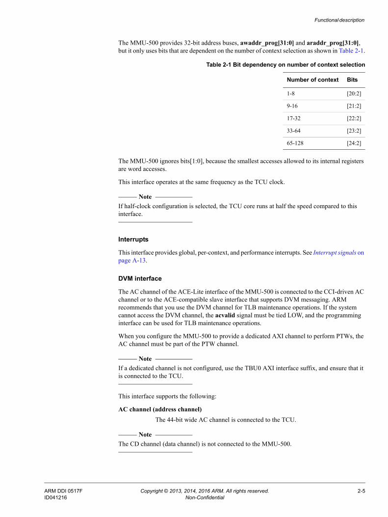
Functional description
The MMU-500 provides 32-bit address buses, awaddr_prog[31:0] and araddr_prog[31:0], but it only uses bits that are dependent on the number of context selection as shown in Table 2-1.
The MMU-500 ignores bits[1:0], because the smallest accesses allowed to its internal registers are word accesses.
This interface operates at the same frequency as the TCU clock.
Note If half-clock configuration is selected, the TCU core runs at half the speed compared to this interface.
Interrupts
This interface provides global, per-context, and performance interrupts. See Interrupt signals on page A-13.
DVM interface
The AC channel of the ACE-Lite interface of the MMU-500 is connected to the CCI-driven AC channel or to the ACE-compatible slave interface that supports DVM messaging. ARM recommends that you use the DVM channel for TLB maintenance operations. If the system cannot access the DVM channel, the acvalid signal must be tied LOW, and the programming interface can be used for TLB maintenance operations.
When you configure the MMU-500 to provide a dedicated AXI channel to perform PTWs, the AC channel must be part of the PTW channel.
Note If a dedicated channel is not configured, use the TBU0 AXI interface suffix, and ensure that it is connected to the TCU.
This interface supports the following:
AC channel (address channel) The 44-bit wide AC channel is connected to the TCU.
Note The CD channel (data channel) is not connected to the MMU-500.
Table 2-1 Bit dependency on number of context selection
Number of context Bits
1-8 [20:2]
9-16 [21:2]
17-32 [22:2]
33-64 [23:2]
65-128 [24:2]
ARM DDI 0517F Copyright © 2013, 2014, 2016 ARM. All rights reserved. 2-5ID041216 Non-Confidential
Functional description
PTW interface
In the MMU-500, there can be a dedicated interface that provides access to memory for page table walks.
If the MMU-500 is configured to support a dedicated interface for PTWs, you must connect the read address and read data channels of the slave interface associated with the PTWs to the MMU-500 PTW channel. In this configuration, the PTW channel contains the _ptw suffix. For example, araddr_ptw and acaddr_ptw.
Note • The write interface on the dedicated PTW interface is not used.
• If the MMU-500 is configured not to support a dedicated interface for PTWs, PTWs are performed on the ACE-Lite interface connected to TBU0.
2.2.2 TBU interfaces
The MMU-500 supports the following TBU interfaces:• ACE-Lite interfaces.
The ACE-Lite interface supports the following interfaces:— AXI slave interface.— AXI master interface on page 2-7.— TBU barrier support on page 2-7.
• Sideband interface on page 2-7.The sideband interface supports the following interfaces:— StreamID interface on page 2-7.— Security State Determination (SSD) interface on page 2-7.
ACE-Lite interfaces
The MMU-500 uses the ACE-Lite interfaces to receive and forward transactions after a translation.
An AXI3 or AXI4 bus can be connected to this interface with certain limitations as described in AXI3 and AXI4 support on page 2-21.
When an ACE-Lite interface is used, the MMU-500 generates barrier transactions and updates attributes of input barrier transactions. Barrier transactions guarantee the ordering and observation of transactions in a system.
For more information on barrier transactions, see the ARM® AMBA® AXI and ACE Protocol Specification AXI3, AXI4, and AXI4-Lite ACE and ACE-Lite.
AXI slave interface
The MMU-500 supports only the ACE-Lite slave interface for every TBU. To connect to an AXI3 or AXI4 interface, you must: • Tie the extra ACE-Lite signals to their inactive values.• Tie the sysbardisable_<tbuname> signal HIGH.
ARM DDI 0517F Copyright © 2013, 2014, 2016 ARM. All rights reserved. 2-6ID041216 Non-Confidential

Functional description
The ACE-Lite slave interface, with _s suffix, drives the untranslated address to the TBU. You must connect pin-to-pin the read address, write address, read data, write data, and buffered write response channels of the ACE-Lite slave interface to an ACE-Lite master interface. In a system, the master interface can be the AXI bus infrastructure output or the output of a bridge that converts another bus protocol to AXI.
AXI master interface
The MMU-500 supports only the ACE-Lite master interface for every TBU. You must tie the extra ACE-Lite signals to their inactive values and the sysbardisable_<tbuname> signal to HIGH to use AXI3 or AXI4 master interfaces.
The ACE-Lite master interface, with _m suffix, drives the translated address to the downstream slave. You must connect pin-to-pin the read address, write address, read data, write data, and buffered write response channels to the corresponding ACE-Lite slave interface.
If the MMU-500 is configured to support a dedicated interface for PTWs, you must connect the read address and read data channels of the slave interface associated with the PTWs to the MMU-500 PTW channel. In this configuration, the PTW channel contains the _ptw suffix. For example, araddr_ptw and acaddr_ptw.
TBU barrier support
The TBU in the MMU-500 receives, passes on, and generates barriers of its own.
The MMU-500 generates a DSBSYS barrier on its own, after ensuring that all invalidation-related transactions are initiated when sysbardisable_<tbuname> is LOW, and on receiving one of the following:• The SYNC message received on the programming interface.• The DVM SYNC message.
For more information on SYNC and DVM SYNC messages, see the ARM® AMBA® AXI and ACE Protocol Specification AXI3, AXI4, and AXI4-Lite ACE and ACE-Lite.
Sideband interface
The sideband interface provides associated information, such as data byte, transfer, packet, or frame-based information along with the ACE-Lite interface. See Sideband signals on page A-13.
Note The StreamID and security state determination are associated with the ACE-Lite slave interface to each TBU.
StreamID interface
The StreamID interface is a sideband interface for the MMU-500 TBU slave interface. It provides additional information about the source of the incoming transaction. This information permits the transaction to be mapped to a particular context for translation.
The MMU-500 samples signals in the interface along with each valid address transaction.
See StreamID on page 2-13.
Security State Determination (SSD) interface
The SSD interface is a sideband interface for the MMU-500 TBU slave interface. It provides information about the security state of a transaction.
ARM DDI 0517F Copyright © 2013, 2014, 2016 ARM. All rights reserved. 2-7ID041216 Non-Confidential

Functional description
The MMU-500 samples signals in this interface along with each valid address transaction, in a similar manner to the StreamID on page 2-13.
See Security determination on page 2-14.
2.2.3 Common interfaces
The MMU-500 supports the following interfaces that are common to TBUs and the TCU:• Low-power interface for clock gating and power control.• Performance interface on page 2-11.• Tie-off signal interface on page 2-11.
Low-power interface for clock gating and power control
The MMU-500 contains Q-channel low-power interfaces that enable:• Power gating of the TBU module.• Clock gating of the TBU module.• Clock gating of the TCU module.
You can control the power-control interfaces at the system level by a system power-control module. Alternatively, if there is no system control block, you must tie the qreqn_* inputs HIGH, and can leave the outputs, qacceptn_* and qactive_* unconnected.
The MMU-500 never denies a powerdown request on any Q-channel, and so you must tie LOW the qdeny_* input to the system power controller.
The TCU module must be powered up before, or at the same time as, any TBU module is powered up. The TCU module must remain powered up while any TBU module is powered up.
Note The low-power interface signals are not synchronized. The system must provide the synchronous signals to the MMU-500.
The MMU-500 provides a Q-channel low-power interface for clock gating support. This interface is used as follows:
• The TBU and TCU have dedicated low-power Q-channel interfaces for clock gating:— qreqn_tbu_<tbuname>_cg, qacceptn_tbu_<tbuname>_cg, and
qactive_tbu_<tbuname>_cg.— qreqn_tcu, qacceptn_tcu, and qactive_tcu.
• The TBU and the clock or power bridge each have a dedicated Q-channel interface for entering the powerdown state:— qreqn_tbu_<tbuname>_pd and qacceptn_tbu_<tbuname>_pd.— qreqn_pd_slv_br_<tbuname> and qacceptn_pd_slv_br_<tbuname>.— qreqn_pd_mst_br_<tbuname> and qacceptn_pd_mst_br_<tbuname>.
• The clock or power bridge contains the following qactive signals:— The qactive_br_tbu_<tbuname> signal for handling the cross-boundary clock
wakeup to wake up the TBU clock.— The qactive_br_tcu_<tbuname> signal for handling the cross-boundary clock
wakeup to wake up the TCU clock.
Figure 2-3 on page 2-9 shows the possible clock and power domains of the MMU-500.
ARM DDI 0517F Copyright © 2013, 2014, 2016 ARM. All rights reserved. 2-8ID041216 Non-Confidential

Functional description
Figure 2-3 Clock and power domains of the MMU-500
Figure 2-4 on page 2-10 shows that TBU0 and TCU share a common clock or power domain. The TCU page table walk read channel shares the AXI interface with the TBU0.
TCU
Deserializer
Asynchronousbridge master
interface
SerializerAsynchronousbridge slave
interface
Asynchronousbridge slave
interface
Asynchronousbridge master
interface
a. AXI stream register slice
TBUn
Interrupts
ACE-Lite slave
interface
ACE-Lite master
interface
GPU
Interconnect
TBUn clock and power domain
TBU0 clock and power domain
TCU clock and power domain
Q channel
DVM channel
Programming channel
Tie-offs
Interconnect
Q-channel power
Q-channel power
Half clockbFull clockTransitionb
b. Present only in the half-clock configurations
TCU-TBU Invalidation
channel
TCU-TBU programming
channel
TCU-TBU fault
channel
TBU-TCU PTW request
channel
TBU-TCUPTW result
channel
Serializer
Deserializer
Register slice
Register slice
Q-channel power
Q-channel clock gate
Register slice
Register slice
Register slicea
Register slicea
Register slicea
Register slicea
Deserializer
Asynchronousbridge master
interface
SerializerAsynchronousbridge slave
interface
Asynchronousbridge slave
interface
Asynchronousbridge master
interface
TBU0
ACE-Lite slave
interface
ACE-Lite master
interface
DMA
Interconnect
Q-channel power
Q-channel power
Serializer
Deserializer
Register slice
Register slice
Q-channel power
Q-channel clock gate
Register slice
Register slice
Register slicea
Register slicea
Register slicea
Register slicea
PTW address
readchannel
PTW read data
channel
ARM DDI 0517F Copyright © 2013, 2014, 2016 ARM. All rights reserved. 2-9ID041216 Non-Confidential

Functional description
Figure 2-4 TBU0 and TCU sharing a common clock or power domain
The full clock to half clock configuration feature shown in Figure 2-3 on page 2-9 and Figure 2-4 is also applicable to:• Interrupts.• Programming interfaces.• PTW interfaces.
If you configure the TCU PTW interface to be shared with the TBU0 master interface by disabling the PTW has a separate AXI port configuration parameter, a multiplexer is instantiated in the design. You can use the multiplexer to share the ACE-Lite interface of TBU0 with the PTW interface generated by the TCU, provided you ensure that the TBU0 data width is the same as that of the TCU.
In this shared configuration, TBU and TCU still have two separate LPI interfaces for clock gating. Consequently, when TBU0 is clock gated, you can still see accesses coming from the TCU PTW interface and being output from the shared TBU0 master interface.
The MMU-500 supports the half clock feature as shown in Figure 2-3 on page 2-9 and Figure 2-4 depending on the specified configuration.
For more information about the Q-channel low-power interface, see the Low Power Interface Specification, ARM® Q-Channel and P-Channel Interfaces.
TCU
Deserializer
Asynchronousbridge master
interface
SerializerAsynchronousbridge slave
interface
Asynchronousbridge slave
interface
Asynchronousbridge master
interface
a. AXI stream register slice
TBUn
Interrupts
ACE-Lite slave
interface
ACE-Lite master
interface
GPU
Interconnect
TBUn clock and power domain TBU0 + TCU clock and power domain
Q channel
DVM channel
Programming channel
Tie-offs
Interconnect
Q-channel power
Q-channel power
Half clockbFull clockTransitionb
b. Present only in the half-clock configurations
TCU-TBU Invalidation
channel
TCU-TBU programming
channel
TCU-TBU fault
channel
TBU-TCU PTW request
channel
TBU-TCUPTW result
channel
Serializer
Deserializer
Register slice
Register slice
Q-channel power
Q-channel clock gate
Register slice
Register slice
Register slicea
Register slicea
Register slicea
Register slicea
Deserializer
Serializer
TBU0
ACE-Lite slave
interfaceDMA Serializer
Deserializer
Register slice
Register slice
Q-channel power
Q-channel clock gate
Register slice
Register slice
Register slicea
Register slicea
Register slicea
Register slicea
ACE-Lite master
interfaceInterconnect PTW
address read
channel
PTW readdata
channel
ARM DDI 0517F Copyright © 2013, 2014, 2016 ARM. All rights reserved. 2-10ID041216 Non-Confidential
Functional description
Performance interface
This interface contains the input signal spniden that enables the counting of events resulting from Secure translations, and contains an event output interface that provides updates from each TBU to the performance counters.
See Performance event signals on page A-15 and Authentication interface signal on page A-14.
Tie-off signal interface
This interface provides configuration information about AXI or ACE-Lite interface operations and page table walk coherency. See Tie-off signals on page A-15.
ARM DDI 0517F Copyright © 2013, 2014, 2016 ARM. All rights reserved. 2-11ID041216 Non-Confidential

Functional description
2.3 OperationThe MMU-500 routes each translation through the following logical processing steps:1. Security state determination.2. Context determination.3. Page table walk, if the translation is not cached in the TLB.4. Protection checks.5. Attribute generation or merging, depending on the programming.
You can configure the MMU-500 to bypass the transaction process for a transaction or to fault a transaction regardless of the translation state.
The primary function of the MMU-500 is to provide address and memory attribute translations, based on the address mapping and memory attribute information stored in translation tables.
The MMU-500 performs the following steps to achieve this:
1. Receives an address transaction, along with security and stream information.
2. Uses the security information received along with a transaction to determine additional processing steps for the transaction. The received security information is the security state of the originator of a transaction. The MMU-500 uses a Secure or Non-secure set of registers for additional processing of a transaction, depending on whether the security state of the originator is Secure or Non-secure, respectively. See Security determination on page 2-14.
3. Uses the (S)CR0.CLIENTPD to determine whether stream matching is required. The transaction is bypassed if CLIENTPD is disabled.
4. Uses the stream information received along with the transaction to determine the translation mechanism to apply to the transaction. The translation mechanism can be a bypass, a stage 1 translation, a stage 2 translation, or a stage 1 followed by stage 2 translation. See the ARM® System Memory Management Unit Architecture Specification.
5. Adds the fault information to the Global Fault Status Register if a fault is identified in the translation process before a context is mapped. The MMU-500 adds the fault information to the Fault Status Register for the context bank, if a fault is identified after the context mapping.A fault results in an interrupt when interrupt reporting is enabled. You can clear interrupts by clearing the Fault Status Register.
Note The MMU-500 does not support configuration errors. It treats the CAF bit in the Global
Fault Status Register as RAZ.
See the ARM® System Memory Management Unit Architecture Specification.
The MMU-500 supports both little and big endian translation tables. You can program endianness in the SMMU_CBn_SCTLR register. See the ARM® Architecture Reference Manual ARMv7-A and ARMv7-R edition.
For information about initialization and configuration, see Additional reading on page viii.
This section describes how the ARM® CoreLink™ MMU-500 System Memory Management Unit operates. It contains the following subsections:• StreamID on page 2-13.• Security determination on page 2-14.
ARM DDI 0517F Copyright © 2013, 2014, 2016 ARM. All rights reserved. 2-12ID041216 Non-Confidential

Functional description
• Hit-Under-Miss on page 2-16.• Fault handling on page 2-17.• Implementation-defined operational features on page 2-17.
2.3.1 StreamID
A StreamID maps the incoming transaction to a context by using the stream mapping table. The characteristics of the StreamID are as follows:
• The width of the StreamID is selected during the MMU-500 configuration.
• You must specify the StreamID on a dedicated AXI sideband signal. Select the StreamID - width of the sideband signal parameter value from the range 1-10 bits or 15 bits. Dedicated sideband signals are used for read and write transactions.
For more information about StreamID signals, see Sideband signals on page A-13.
When the StreamID is configured as 1-10 bits The StreamID width in the TCU is a constant 15 bits. The MMU-500 zero-extends each TBU StreamID to form a 10-bit field that it appends to the 5-bit TBU ID field, making the StreamID the required 15 bits wide by the time it reaches the TCU.When the StreamID presented to each TBU is not unique
You must ensure that a unique ID is presented to the TCU, by appending the StreamID to the 5-bit TBU ID field as shown in Figure 2-5.
Figure 2-5 StreamID is not unique
When the StreamID presented to each TBU is unique If the StreamID presented to each TBU is already unique, and the TBU ID addition is not required, then you can use the SMR to mask the TBU ID if required, as shown in Figure 2-6 on page 2-14.
Master
TBU1
TBU2
TBUn
TCU
10000
000010000010000
000100000010000
100000000010000
10-bit zero-extended StreamID5-bit TBUID
10000
StreamID 10000
ARM DDI 0517F Copyright © 2013, 2014, 2016 ARM. All rights reserved. 2-13ID041216 Non-Confidential

Functional description
Figure 2-6 StreamID is unique
When the StreamID is configured as 15 bits The StreamID widths in the TBU and the TCU are both 15 bits, meaning that the TBU ID is not appended.
For more information on StreamID-to-context mapping, see the ARM® System Memory Management Unit Architecture Specification.
2.3.2 Security determination
The MMU-500 determines the Secure ownership of a transaction in one of the following ways:
• Assigns the Non-secure state to an incoming sideband signal along with a transaction:— For write accesses, the Non-secure state is the write sideband signal for security.
Writes The security state is taken from wsb_ns_<tbuname>_s. The value of the SSD index can be:0 Indicates Secure access.1 Indicates Non-secure access.
— For read accesses, the Non-secure state is the read sideband signal for security.Reads The security state is taken from rsb_ns_<tbuname>_s. The value of the
SSD index can be:0 Indicates Secure access.1 Indicates Non-secure access.
• Determines the security state of a master by using the input signals, wsb_ssd_<tbuname>_s and rsb_ssd_<tbuname>_s. These signals form an SSD index into the SSD table. The entry in the SSD table determines whether the master that initiated the transaction is Secure or Non-secure. For more information about SSD signals, see Sideband signals on page A-13.— You can configure the width of the SSD index in the range 0-10 bits. The MMU-500
uses a separate SSD index for each TBU.
Master
TBU1
TBU2
TBUn
Stream Match Register
10000
000010000010000
000100000011000
100000000011100
10-bit zero-extended StreamID
5-bit TBUID
11100
StreamID 11000
000000000010000
000000000011000
000000000011100
TCU
10-bit zero-extended StreamID
5-bit TBUID masked by SMR
ARM DDI 0517F Copyright © 2013, 2014, 2016 ARM. All rights reserved. 2-14ID041216 Non-Confidential

Functional description
— You can configure the number of programmable entries in the SSD table in the range 1- (Number of TBU * 8). The security state determination address space supports 15-bit wide SSD indices. This space is equally divided among 32 TBUs starting with TBU0 from the address 0x0 of the address space. Each TBU contains 1024 entries.
— You can program the security state of the SSD table entries at runtime, or specify the non-programmable and fixed SSD table entries at configuration time.
After the SSD index is determined, the SSD table contains bits from 0 to 2SSD index signal width-1. You must determine the status of the bits as follows:
An SSD index can be programmable or non-programmable, and can be in the Secure or Non-secure state. By default, an SSD index is in the non-programmable Non-secure state.
List of non-programmable indices For these indices, the security state of the master is defined, and does not change.You must specify the indices of the masters whose security states are always Secure.
List of programmable indices You can program the security state of the programmable indices.You must determine the default state of each master whose security state is programmable.
Note An entry must not be duplicated in more than one list.
You must specify at least one programmable or fixed Non-secure entry for every configuration.
The number of indices is determined by the configured SSD index signal width. For example, if the SSD index signal width is 6 bits, there are 64 indices in the range 0-63. You must program the indices to be one of:• Programmable Secure. • Programmable Non-secure. • Non-programmable Secure.
The unprogrammed indices default to non-programmable Non-secure.
The MMU-500 supports Secure debug TLB accesses that can access Secure and Non-secure TLBs.
The SSD table has a maximum of 32Kb space that is divided into 32 parts, with 1Kb assigned to each TBU. For example, the TBU0 space is from 0-1Kb, the TBU1 space is from 1-2Kb, and the TBU2 space is from 2-3Kb. The SSD index that is generated at each TBU, and is a maximum of 10 bits, is indexed into the 1Kb space allocated to the TBU. You must program the SSD table using this information.
Note The security determination descriptions are valid when the integ_sec_override signal is set to zero.
ARM DDI 0517F Copyright © 2013, 2014, 2016 ARM. All rights reserved. 2-15ID041216 Non-Confidential

Functional description
When the integ_sec_override signal is set to one, the following conditions are true:
• All implementation and integration registers can be accessed with a Non-secure access. This includes the following global space 0 registers: — Auxiliary Configuration Register (ACR).— Debug registers.
• You cannot access any Secure registers.
• All transactions are treated as originating from a Non-secure master.
For more information on security determination and extensions, see the ARM® System Memory Management Unit Architecture Specification.
2.3.3 Hit-Under-Miss
Hit-Under-Miss (HUM) translates a TLB miss transaction and passes the transaction to a downstream slave if the translated TLB miss transaction results in a TLB hit. HUM allows responding to the master if there is a TLB hit for a subsequent transaction while the MMU-500 is performing a translation for a previous transaction that had a TLB miss. HUM characteristics for read and write transactions are as follows:
• If the transactions are read accesses, HUM is automatically enabled.
• If the transactions are write operations, HUM is enabled or disabled based on the write buffer depth. You can specify the write buffer depth during configuration.— If the depth of the write buffer is zero, HUM is automatically disabled.— If the depth of the write buffer is non-zero, a write hit transaction is translated only
if the write data from a missed transaction can be accommodated in the write buffer.
• The number of outstanding missed transactions is determined by the depth of the write buffer. For example, if the depth of the buffer is four, then it can hold two transactions of length two. Each buffer entry holds only one beat of the transaction, even if it is of a narrow width.
Example 2-1 shows a HUM condition.
Example 2-1 HUM condition
Consider that the write buffer depth is eight and there are two missed write transactions of lengths four and three. Both missed write transactions are stored in the write buffer during the PTWs for the transactions. If you perform another transaction before the missed write transactions are processed, the new transaction is passed through, if that access results in a TLB hit.
Note If the write buffer is full with missed write transactions, HUM cannot occur.
ARM DDI 0517F Copyright © 2013, 2014, 2016 ARM. All rights reserved. 2-16ID041216 Non-Confidential

Functional description
2.3.4 Fault handling
The MMU-500 supports the terminate and stall fault handling modes. However, the MMU-500 does not support fault model overrides from the global space specified by using the Global Stall Enable (GSE) and Stall Disable (STALLD) bits of the Secure Configuration Register, SMMU_CR0 or SMMU_sCR0.
If the Hit Under Previous Context Fault (HUPCF) bit of the SMMU_CBn_SCTLR is not enabled, the MMU-500 applies the fault model across TBUs that share the same context.
For more information on fault handling. See the ARM® System Memory Management Unit Architecture Specification.
2.3.5 Implementation-defined operational features
The operational features of the MMU-500 are described in the following sections:• Outstanding transactions per TBU.• QoS arbitration.• Address width on page 2-18.• Programmable QoS support in the TCU on page 2-18.
Outstanding transactions per TBU
Outstanding transactions are defined as transactions for which:• The physical address access is generated and accepted by the slave.• Write or read responses are stalled.
For every TBU, the MMU-500 supports 256 outstanding transactions each for write and read accesses.
The MMU-500 generates a PTW when accesses from the master result in a TLB miss. However, based on the configuration, the MMU-500 supports either 8 or 16 such parallel PTWs for a TBU. If more than 8 or 16 PTWs are pending, a TLB miss on a channel indicates that the MMU-500 cannot accept additional transactions on the write or read channels.
QoS arbitration
The PTWs are initiated by the TCU for multiple TBUs. Therefore, when there are multiple outstanding transactions in the TCU, priority is given to the TBU with the highest QoS. The MMU-500 reuses the programmed QoS value for PTWs.
The arqosarb signal, a sideband signal from the MMU-500 to the CCI, has the highest QoS value among all PTW read transactions in the TCU.
Note You can leave the unused output ports unconnected.
For address translations, the MMU-500 uses the programmed QoS value.
For individual prefetch accesses, the MMU-500 uses the QoS value of the hit transaction.
For transactions within the same QoS, the MMU-500 uses a first-come, first-served model.
ARM DDI 0517F Copyright © 2013, 2014, 2016 ARM. All rights reserved. 2-17ID041216 Non-Confidential

Functional description
Address width
The incoming address width is fixed at 49 bits, where A[48] specifies VA sub-ranges. You must tie all unused bits to zero. The output address width is 48 bits and the width of the AC address bus is 48 bits.
Note The MMU-500 does not support peripherals whose address width is greater than 49 bits.
Programmable QoS support in the TCU
You can program the QoS value to be used for each TBU PTW in the TCU. See TBU QoS registers on page 3-33.
ARM DDI 0517F Copyright © 2013, 2014, 2016 ARM. All rights reserved. 2-18ID041216 Non-Confidential

Functional description
2.4 Cache structures of the MMU-500The cache structures of the MMU-500 are described in the following sections:• Micro TLB.• Macro TLB.• Prefetch buffer on page 2-20.• Page table walk cache on page 2-20.• IPA to PA cache on page 2-20.
2.4.1 Micro TLB
The micro TLB in the TBU caches the PTW results returned by the TCU. The TBU compares the PTW results of incoming transactions with the entries in the micro TLB before performing a TCU PTW. The micro TLB is fully associative and you can configure the depth of a micro TLB based on your requirements.
Figure 2-7 shows the micro TLB cache structure.
Figure 2-7 Micro TLB cache
See Additional reading on page viii for more information on the TBU configurability.
2.4.2 Macro TLB
The macro TLB caches PTW results in the TCU. You can configure the depth of the macro TLB based on your requirements.
Figure 2-8 shows the TCU cache structure that consists of macro TLBs, prefetch buffers, IPA2PA cache, and PTW caches.
Figure 2-8 TCU cache
TBU0 TBU1 TBUna
Micro TLB RAM
Micro TLB RAM
Micro TLB RAM
a. n is number of RAMs configured.
Cache
TCU
Macro TLBandPTW cache
Prefetch buffer IPA to
PA cache
ARM DDI 0517F Copyright © 2013, 2014, 2016 ARM. All rights reserved. 2-19ID041216 Non-Confidential

Functional description
See Additional reading on page viii for more information on the TCU configurability.
2.4.3 Prefetch buffer
The MMU-500 fetches in advance 4KB and 64KB sized pages into the prefetch buffer. This reduces latency for future PTWs. You can configure the depth of the prefetch buffer.
The prefetch buffer is a single four-way set associative cache that you can enable or disable, depending on the context. The prefetch buffer shares RAMs with the macro TLB cache. See Macro TLB on page 2-19.
2.4.4 Page table walk cache
The MMU-500 caches partial PTWs to reduce the number of PTWs on a TLB miss. The PTW cache exists in the TCU, and stage 1 and stage 2 level 2 PTWs are cached in the PTW cache.
2.4.5 IPA to PA cache
The MMU-500 implements an IPA to PA cache for stage 1 followed by stage 2 translations.
The IPA to PA cache is a single four-way set associative cache that you can enable or disable depending on the context. The IPA to PA cache shares RAMs with the PTW cache. See Page table walk cache.
ARM DDI 0517F Copyright © 2013, 2014, 2016 ARM. All rights reserved. 2-20ID041216 Non-Confidential

Functional description
2.5 Constraints and limitations of useThis section describes the constraints of the MMU-500.
2.5.1 AXI3 and AXI4 support
The MMU-500 supports the AXI3 and AXI4 protocols when the sysbardisable_<tbuname> input signal is tied HIGH. In such cases, the following AXI3 features are not supported:
Write data interleaving Write data and write address ordering must be the same, otherwise data corruption can occur.
Locked transfer The input interface on a TBU contains only one bit of the AWLOCK and ARLOCK signals to ensure compliance with the AXI4 specification. Therefore, locked transfers are not supported even when the sysbardisable_<tbuname> signal is HIGH.
The WID signal generation The MMU-500 does not generate the WID signals for the TBU write data channels because these signals are not required for AXI4 and ACE-Lite. You must add logic to generate the WID signal based on the WID signal values that are used for the address channel transfer, and use the values for each write data channel transfer for a transaction.The MMU-500 does not support write data interleaving. Therefore, the MMU-500 generates write data transfers in the sequence that the write addresses are issued.Example 2-2 shows a scenario to generate the WID signal.
Example 2-2 Generating the WID signal
At the slave interface, you can connect the WID signal to the WUSER signal. At the master interface, you can generate WID by connecting WID to the same bit positions of the WUSER signal as at the slave interface.
See the ARM® AMBA® AXI and ACE Protocol Specification AXI3, AXI4, and AXI4-Lite ACE and ACE-Lite for more information about the WID and WUSER signals.
Unused ACE-Lite ports If an AXI3 interface is connected to an ACE-Lite port, then the unused ACE-Lite signals must be tied off to the values shown in Table 2-2.
Table 2-2 Unused ACE-Lite signals
Signal name value
axregion b00
axqos b00
axbar b00
axdomain b11
axsnoop b00
ARM DDI 0517F Copyright © 2013, 2014, 2016 ARM. All rights reserved. 2-21ID041216 Non-Confidential

Functional description
Normalization of memory attributes Most ARMv8 processors generate a normalized version of the memory attribute. See SMMU_sACR register bit assignments on page 3-15.By programming the SMMU_SACR.NORMALIZE bit, you can enable the normalization support.
Note You have to enable the normalization support only when the MMU-500 is
instantiated in the ARMv8 system.
ARM DDI 0517F Copyright © 2013, 2014, 2016 ARM. All rights reserved. 2-22ID041216 Non-Confidential

Chapter 3 Programmers model
The MMU-500 requires a programming interface to enable the software to configure the controller. You can also use the programming interface as a debug interface for accessing the TLB information.
This chapter describes the MMU-500 registers and provides information about programming the MMU-500. It contains the following sections:• About this programmers model on page 3-2.• Modes of operation and execution on page 3-3.• Memory model on page 3-4.• Register summary on page 3-9.• Global address space 0 on page 3-12.• Global address space 1 on page 3-24.• Translation context address space on page 3-25.• Integration registers on page 3-26.• Peripheral and component identification registers on page 3-36.
ARM DDI 0517F Copyright © 2013, 2014, 2016 ARM. All rights reserved. 3-1ID041216 Non-Confidential

Programmers model
3.1 About this programmers modelThe following information applies to the MMU-500 registers:
• Registers are implemented according to the ARM® System Memory Management Unit Architecture Specification with the security extensions implemented in the MMU-500 as follows: — Global space 0 registers summary on page 3-9.— Translation context registers summary on page 3-9.— Integration registers summary on page 3-10.— Peripheral and component identification summary on page 3-10.
• Unless otherwise stated in the accompanying text:— Do not modify undefined register bits.— Ignore undefined register bits on reads.— All register values are UNKNOWN on reset unless otherwise stated.
• The access types of the MMU-500 registers are as follows:RAO Read-As-One.RAO/SBOP Read-As-One, Should-Be-One-or-Preserved on writes.RAO/WI Read-As-One, Writes-ignored.RAZ Read-As-Zero.RAZ/SBZP Read-As-Zero, Should-Be-Zero-or-Preserved on writes.RAZ/WI Read-As-Zero, Write-ignored.RO Read-only.RW Read and write.SBO Should-Be-One.SBOP Should-Be-One-or-Preserved.SBZ Should-Be-Zero.SBZP Should-Be-Zero-or-Preserved.UNK Unknown.WI Write-ignored.WNR Write-not-read.WO Write-only.
3.1.1 Dynamic programming
The MMU-500 allows dynamic programming as specified by the architecture. See the ARM® System Memory Management Unit Architecture Specification for more information.
ARM DDI 0517F Copyright © 2013, 2014, 2016 ARM. All rights reserved. 3-2ID041216 Non-Confidential

Programmers model
3.2 Modes of operation and execution
The MMU-500 provides a 64-bit AXI4 programming interface as per the ARM® AMBA® AXI and ACE Protocol Specification AXI3, AXI4, and AXI4-Lite ACE and ACE-Lite. The interface restrictions are as follows:
• A single combined acceptance depth is used for write and read channels.
• All 32-bit register write accesses must:— Be one beat long.— Be used for a word-aligned location.— Be 32 bits wide.— Have all relevant write strobes set.If any of these conditions is not met, the MMU-500 ignores the transaction.
• All 64-bit register write accesses must satisfy one of the following conditions:— Be one beat long, 64 bits wide, used for a double-word aligned location, and have
all write strobes set. — Be two beats long, 32 bits wide, used for a double-word aligned location, and have
all relevant write strobes set.— Be one beat long, 32 bits wide, used for a word aligned location, and have all
relevant write strobes set.If any of these conditions is not met, the MMU-500 ignores the transaction.
• The AXI4 programming interface does not log errors or issue error responses. It treats invalid accesses as either RAZ or WI.
• The AXI4 programming interface ignores the AxBURST, AxLOCK, AxCACHE, AxQOS, AxREGION, and AxUSER signals.
• If a master connected to the MMU-500 generates a FIXED-type burst, and if the translated domain is a shared DOMAIN (Inner-shared or Outer-shared), then the MMU-500 generates an Unsupported Upstream Transaction (UUT) fault. — For single-beat transfers, a master can generate an INCR type burst to avoid this
problem.— For multi-beat transfers, the MMU-500 cannot avoid this problem, and the system
must generate the ouput DOMAIN value as Non-shared or System-shared.
ARM DDI 0517F Copyright © 2013, 2014, 2016 ARM. All rights reserved. 3-3ID041216 Non-Confidential

Programmers model
3.3 Memory model
The address map of the programming interface is consistent with the ARM® System Memory Management Unit Architecture Specification.
In addition to the registers specified in the ARM® System Memory Management Unit Architecture Specification, the MMU-500 implements the following configuration, identification, debug, context, integration, performance, and control registers:• Non-secure Auxiliary Configuration Register (SMMU_ACR).• Secure Auxiliary Configuration Register (SMMU_sACR).• TBU-TLB Debug Read Pointer register (SMMU_DBGRPTRTBU).
TBU-TLB Debug Read Data register (SMMU_DBGRDATATBU).• TCU-TLB Debug Read Pointer register (SMMU_DBGRPTRTCU).• TCU-TLB Debug Read Data register (SMMU_DBGRDATATCU).• Auxiliary Control Register (SMMU_CBn_ACTLR).• Integration Mode Control register (SMMU_ITCTRL).• Integration Test Input register (SMMU_ITIP).• Integration Test Output Global register (SMMU_ITOP_GLBL). • TBU Performance Interrupt register (SMMU_ITOP_PERF_INDEX).• Integration Test Output Context Interrupt registers (SMMU_ITOP_CXTnTOm_RAMx):
— Register for contexts 0-31 (SMMU_ITOP_CXT0TO31_RAM0).— Register for contexts 32-63 (SMMU_ITOP_CXT32TO63_RAM1).— Register for contexts 64-95 (SMMU_ITOP_CXT64TO95_RAM2).— Register for contexts 96-127 (SMMU_ITOP_CXT96TO127_RAM3).
• TBU QoS registers (SMMU_TBUQOSx):— TBU QoS register 0 (SMMU_TBUQOS0).— TBU QoS register 1 (SMMU_TBUQOS1).— TBU QoS register 2 (SMMU_TBUQOS2).— TBU QoS register 3 (SMMU_TBUQOS3).
• Parity Error Checker Register (SMMU_PER). • TBU Power Status Register (SMMU_TBU_PWR_STATUS).• Component Identification registers (SMMU_CIDRn):
— Component Identification register 0 (SMMU_CIDR0).— Component Identification register 1 (SMMU_CIDR1).— Component Identification register 2 (SMMU_CIDR2).— Component Identification register 3 (SMMU_CIDR3).
• Peripheral Identification registers (SMMU_PIDRn):— Peripheral Identification register 0 (SMMU_PIDR0).— Peripheral Identification register 1 (SMMU_PIDR1).— Peripheral Identification register 2 (SMMU_PIDR2).— Peripheral Identification register 3 (SMMU_PIDR3).— Peripheral Identification register 4 (SMMU_PIDR4).— Peripheral Identification registers 5-7 (SMMU_PIDR5-7).
The MMU-500 does not support the following Global Space Invalidation registers for stage 2 configurations:• SMMU_STLBIALLM.• SMMU_TLBIVMIDS1.• SMMU_TLBIVALH.• SMMU_STLBIVAM.
ARM DDI 0517F Copyright © 2013, 2014, 2016 ARM. All rights reserved. 3-4ID041216 Non-Confidential

Programmers model
• SMMU_STLBIVALM.• SMMU_TLBIVAH.• SMMU_TLBIALLH.• SMMU_STLBIALL.
Note The SMMU_SCR1.NSNUMCBO bit field is RO for Only stage 2 translations configurations.
The MMU-500 is configured through a memory-mapped register frame. The total size of the MMU-500 address range depends on the number of implemented translation contexts.
The MMU-500 address map consists of the following equally-sized regions:
The global address space The global address space is located at the bottom of the MMU-500 address space, at SMMU_BASE. See Figure 3-1.
The translation context bank address space The translation context bank address space is located above the top of the global address space, at SMMU_TOP. See Figure 3-1.
Figure 3-1 MMU-500 address map
You can determine the MMU-500 address range by reading the value of the following register fields: • SMMU_IDR1.PAGESIZE.
Note The PAGESIZE refers to the size of the internal memory map, not the MMU-500
translation granule size.
• SMMU_IDR1.NUMPAGENDXB.
See the ARM® System Memory Management Unit Architecture Specification for more information.
You can program the context page size as 4KB or 64KB using the SMMU_SACR.PAGESIZE bit. This bit can be programmed only when the MMU-500 is inactive.
Note The MMU-500 ignores non-word aligned write accesses to any of the registers.
3.3.1 Reset values• MMU-500 Identification registers on page 3-6.• MMU-500 Performance Monitor registers on page 3-7.
Translation context bank address space
Global address spaceSMMU_BASE
SMMU_TOP
SMMU_CB_BASESMMU_GLOBAL_TOP
ARM DDI 0517F Copyright © 2013, 2014, 2016 ARM. All rights reserved. 3-5ID041216 Non-Confidential

Programmers model
MMU-500 Identification registers
Table 3-1 shows the register field reset values for the MMU-500 Identification registers.
Table 3-1 Reset values of SMMU_IDR registers, both Secure and Non-secure
Register field Bitsa Reset values
SMMU_IDR0
SMMU_IDR0.SES [31] 0x1
SMMU_IDR0.S1TS [30] 0x0 Stage 1 translation is not supported.0x1 Stage 1 translation is supported.
SMMU_IDR0.S2TS [29] 0x1
SMMU_IDR0.NTS [28] 0x0 Stage 1 followed by stage 2 translation is not supported.0x1 Stage 1 followed by stage 2 translation is supported.
SMMU_IDR0.SMS [27] 0x1
SMMU_IDR0.ATOSNS [26] 0x1
SMMU_IDR0.PTFS [25:24] 0x0 Stage 1 followed by stage 2 translation is supported.0x1 V7L and V7S supported, and V7L format supported.
SMMU_IDR0.NUMIRPT[7:0] [23:16] 0x01
SMMU_IDR0.CTTW [14] 0x0
SMMU_IDR0.BTM [13] 0x1
SMMU_IDR0.NUMSIDB[3:0] [12:9] 0xF
SMMU_IDR0.NUMSMRG[7:0] [7:0] SMR DEPTH
SMMU_IDR1
SMMU_IDR1.PAGESIZE [31] 0x0
SMMU_IDR1.NUMPAGENDXB [30:28] The reset values for the following contexts are: 1-8 contexts 0x2.9-16 contexts 0x3.17-32 contexts 0x4.33-64 contexts 0x5.64-128 contexts 0x6.
SMMU_IDR1.NUMS2CB[7:0] [23:16] 0x0
SMMU_IDR1.SMCD [15] 0x0
SMMU_IDR1.SSDTP [12] The possible reset values for SMMU_sIDR1.SSDTP (Secure) are: 0x0 Number of SSD entries is zero.0x1 Number of SSD entries is not zero.The reset value for SMMU_IDR1.SSDTP (Non-secure) is 0x0.
Note This bit is configuration-dependent. This bit can have one of the following reset values:0 When the SSD table is not configured.1 When the SSD table is configured.
ARM DDI 0517F Copyright © 2013, 2014, 2016 ARM. All rights reserved. 3-6ID041216 Non-Confidential

Programmers model
MMU-500 Performance Monitor registers
The reset value of the Performance Monitor registers is 0x0, except for the registers that Table 3-2 shows. See the ARM® System Memory Management Unit Architecture Specification for more information.
SMMU_IDR1.NUMSSDNDXB[3:0] [11:8] SMMU_sIDR1.NUMSSDNDBB[3:0] (Secure) 0xF
SMMU_IDR1.NUMSSDNDBB[3:0] (Non-secure) 0x0
SMMU_IDR1.NUMCB [7:0] Number of contexts.
SMMU_IDR2
Reserved [31:15] 0x0
SMMU_IDR2.PTFSv8_64kB [14] 0x1
SMMU_IDR2.PTFSv8_16kB [13] 0x0
SMMU_IDR2.TFSv8_4kB [12] 0x1
SMMU_IDR2.UBS [11:8] 0x5
SMMU_IDR2.OAS [7:4] 0x5
SMMU_IDR2.IAS [3:0] 0x5
SMMU_IDR7
SMMU_IDR7.MAJOR [7:4] 0x2
SMMU_IDR7.MINOR [3:0] 0x4
a. The reserved bits are not shown in Table 3-1 on page 3-6. See the ARM® System Memory Management Unit Architecture Specification for more information.
Table 3-1 Reset values of SMMU_IDR registers, both Secure and Non-secure (continued)
Register field Bitsa Reset values
Table 3-2 Reset values of Performance Monitor Extension registers
Register field Bitsa Reset values
SMMU_PMCGCR.CGNC [27:24] 0x4
SMMU_PMCEID0.EVENT [18:16] 0x7
[10:8] 0x7
[1:0] 0x3
SMMU_PMAUTHSTATUS.SNI [7] 0x1
SMMU_PMDEVTYPE.T [7:4] 0x5
SMMU_PMDEVTYPE.C [3:0] 0x6
SMMU_PMCFGR.NCG [31:24] Number of TBU - 1
SMMU_PMCFGR.UEN [19] 0x0
SMMU_PMCFGR.SIDG [18:17] 0x0
ARM DDI 0517F Copyright © 2013, 2014, 2016 ARM. All rights reserved. 3-7ID041216 Non-Confidential

Programmers model
SMMU_PMCFGR.EX [16] 0x1
SMMU_PMCFGR.CCD [15] 0x0
SMMU_PMCFGR.CC [14] 0x0
SMMU_PMCFGR.SIZE [13:8] 0x1F
SMMU_PMCFGR.N [7:0] (Number of TBU * 4) - 1
SMMU_PMCNTENSETx [31:0] 0x0
SMMU_PMCNTENCLRx [31:0] 0x0
SMMU_PMOVSSETx [31:0] 0x0
SMMU_PMOVSCLRx [31:0] 0x0
a. The reserved bits are not shown in Table 3-2 on page 3-7. See the ARM® System Memory Management Unit Architecture Specification for more information.
Table 3-2 Reset values of Performance Monitor Extension registers (continued)
Register field Bitsa Reset values
ARM DDI 0517F Copyright © 2013, 2014, 2016 ARM. All rights reserved. 3-8ID041216 Non-Confidential

Programmers model
3.4 Register summaryThis section describes the implemented MMU-500 registers in base offset order. The register map contains the following blocks:• Global address space 0 registers summary.• Translation context bank registers summary.• Integration registers summary on page 3-10.• Peripheral and component identification registers summary on page 3-10.
3.4.1 Global address space 0 registers summary
Table 3-3 shows the global space 0 registers in base offset order.
Note The addresses that are not shown in Table 3-3 are reserved.
3.4.2 Translation context bank registers summary
Table 3-4 shows the context registers in base offset order.
Table 3-3 Global space 0 registers summary
Name Type S or NSa Offset Description Notes
SMMU_ACR RW NS 0x00010 Auxiliary Configuration registers on page 3-12
-
SMMU_sACR S Banked with security.
SMMU_DBGRPTRTBU RW S 0x00080 Debug registers on page 3-16 -
SMMU_DBGRDATATBU RO S 0x00084 -
SMMU_DBGRPTRTCU RW S 0x00088 -
SMMU_DBGRDATATCU RO S 0x0008C -
a. S stands for Secure and NS stands for Non-secure.
Table 3-4 Translation context registers summary
Name Type S or NSa Offset Description Notes
SMMU_CBn_ACTLR RW NS/S 0x004 Auxiliary Control registers on page 3-25 -
a. S stands for Secure and NS stands for Non-secure.
ARM DDI 0517F Copyright © 2013, 2014, 2016 ARM. All rights reserved. 3-9ID041216 Non-Confidential

Programmers model
3.4.3 Integration registers summary
Table 3-5 shows the integration registers in base offset order.
3.4.4 Peripheral and component identification registers summary
Table 3-6 shows the peripheral and component identification registers in base offset order.
Table 3-5 Integration registers summary
Name Type S or NS Offset Description
SMMU_ITCTRL RW NS/S 0x2000 Integration Mode Control Register on page 3-26
SMMU_ITIP RO NS/S 0x2004 Integration Test Input register on page 3-27
SMMU_ITOP_GLBL WO NS/S 0x2008 Integration Test Output Global register on page 3-28
SMMU_ITOP_PERF_INDEX WO NS/S 0x200C TBU Performance Interrupt register on page 3-29
SMMU_ITOP_CXTnTOm_RAMx• SMMU_ITOP_CXT0TO31_RAM0• SMMU_ITOP_CXT32TO63_RAM1• SMMU_ITOP_CXT64TO95_RAM2• SMMU_ITOP_CXT96TO127_RAM3
WO NS/S0x2010
0x2014
0x2018
0x201C
Integration Test Output Context Interrupt registers on page 3-32
SMMU_TBUQOSx• SMMU_TBUQOS0• SMMU_TBUQOS1• SMMU_TBUQOS2• SMMU_TBUQOS3
RW NS/S0x2100
0x2104
0x2108
0x210C
TBU QoS registers on page 3-33
SMMU_PER RW NS/S 0x2200 Parity Error Checker Register on page 3-34
SMMU_TBU_PWR_STATUS RW NS/S 0x2204 TBU Power Status register on page 3-34
Table 3-6 Peripheral and component identification summary
Name Type S or NS Offset Description
SMMU_PIDR4 RO NS/S 0x0FD0 Peripheral Identification registers on page 3-36
SMMU_PIDR5 RO NS/S 0x0FD4
SMMU_PIDR6 RO NS/S 0x0FD8
SMMU_PIDR7 RO NS/S 0x0FDC
SMMU_PIDR0 RO NS/S 0x0FE0
SMMU_PIDR1 RO NS/S 0x0FE4
SMMU_PIDR2 RO NS/S 0x0FE8
SMMU_PIDR3 RO NS/S 0x0FEC
SMMU_CIDR0 RO NS/S 0x0FF0 Component Identification registers on page 3-36
SMMU_CIDR1 RO NS/S 0x0FF4
SMMU_CIDR2 RO NS/S 0x0FF8
SMMU_CIDR3 RO NS/S 0x0FFC
ARM DDI 0517F Copyright © 2013, 2014, 2016 ARM. All rights reserved. 3-10ID041216 Non-Confidential

Programmers model
Note The peripheral and component identification registers can be accessed through the SMMU_GR0 register.
ARM DDI 0517F Copyright © 2013, 2014, 2016 ARM. All rights reserved. 3-11ID041216 Non-Confidential

Programmers model
3.5 Global address space 0The MMU-500 global address space 0 provides high-level control of the MMU-500 resources, and maps device transactions to translation context banks. This section provides information about the following registers: • Auxiliary Configuration registers.• Debug registers on page 3-16.
3.5.1 Auxiliary Configuration registers
The SMMU_ACR and SMMU_sACR characteristics are:
Purpose The Auxiliary Configuration registers, SMMU_ACR (Non-secure) and SMMU_sACR (Secure), are defined as shown in Table 3-7 on page 3-13 and Table 3-8 on page 3-15 respectively.
Configuration Available in all MMU-500 configurations.
Usage constraints The S2WC2EN bit is Non-secure only. Other bits are banked with security.
Attributes See Global address space 0 registers summary on page 3-9.
Figure 3-2 shows the bit assignments.
Figure 3-2 SMMU_ACR register bit assignments
31 0
Reserved
1237891011
S2CRB_TLBENMMUDISB_TLBENSMTNMB_TLBEN
S1WC2ENReserved
DP4K_TCUDISB
Reserved
S2WC2EN
4
Reserved
5
IPA2PA_CEN
2324
DP4K_TBUDISB
2526
CACHE_LOCK
27
ARM DDI 0517F Copyright © 2013, 2014, 2016 ARM. All rights reserved. 3-12ID041216 Non-Confidential

Programmers model
Table 3-7 shows the bit assignments.
Table 3-7 SMMU_ACR register bit assignments
Bits Name Reset value Description
[31:27] Reserved - Reserved.
[26] CACHE_LOCK 0b1 Locks the write access to the SMMU_CBn_ACTLR.The SMMU_ACR.CACHE_LOCK bit can have one of the following values:0b0 The SMMU_CBn_ACTLR in all Non-secure contexts is R/W.0b1 The SMMU_CBn_ACTLR in all Non-secure contexts is RO.
[25] DP4K_TBUDISB 0b0 4KB page size dependency check. Enables or disables the 4KB page size dependency check in the TBU. Transactions form a dependency on a transaction that is already performing the PTW. The preconditions are that they are within the same 4KB address space and have the same StreamID and security state as the transaction performing the PTW. This is the default behavior that you can change by programming the bits to not set the dependency. This results in extra latencies and power consumption, and is intended only for debug purposes.This bit resets to zero. When it is set to one, the 4KB dependency check in the TBU is disabled.
[24] DP4K_TCUDISB 0b0 4KB page size dependency check. Enables or disables the 4KB page size dependency check in the TCU.This bit resets to zero. When it is set to one, the 4KB dependency check in the TCU is disabled.
[23:11] Reserved - Reserved.
[10] S2CRB_TLBEN 0b0 Stream-to-context register bypass TLB enable. This bit can have one of the following values:0b0 Do not update the TLB with the stream-to-context register bypass
transaction information.0b1 Update the TLB with the stream-to-context register bypass
transaction information.
Note For the S2CRB_TLBEN, MMUDISB_TLBEN, and SMTNMB_TLBEN bits, the bypass TLB enable bits ensure that the latency is minimal for additional transactions that must undergo the same bypass. However, this comes with the penalty of a TLB entry being occupied for the bypass entry that reduces the effective depth of the TLB available for caching translation operations.
[9] MMUDISB_TLBEN 0b0 MMU disable bypass TLB enable. The MMU-500 caches in the TLB the attribute information for transactions that have been allocated a context, but the SMMU_CBn_SCTLR.M bit is set to 0b0 for the context.This caching reduces the transaction time by six clock cycles, but can save much more, depending on how busy the MMU-500 is.This bit can have one of the following values:0b0 Do not update the TLB with the MMU disable transaction
information.0b1 Update the TLB with the MMU disable transaction information.
ARM DDI 0517F Copyright © 2013, 2014, 2016 ARM. All rights reserved. 3-13ID041216 Non-Confidential

Programmers model
Figure 3-3 shows the bit assignments.
Figure 3-3 SMMU_sACR register bit assignments
[8] SMTNMB_TLBEN 0b0 Stream match table no match TLB enable. This bit can have one of the following values:0b0 Do not update the TLB with the stream match table no match TLB
enable bypass transaction information.0b1 Update the TLB with the stream match table no match TLB
enable bypass transaction information.
[7:5] Reserved - Reserved.
[4] IPA2PA_CEN 0b1 IPA to PA cache enable. This bit can have one of the following values:0b0 Disable the IPA to PA cache.0b1 Enable the IPA to PA cache.
Note This bit is reserved when the Only stage 2 translations option is enabled.
[3] S2WC2EN 0b1 Stage 2 PTW cache 2 enable. The MMU-500 caches the level 2 PTWs in the stage 2 PTW cache 2. This bit can have one of the following values:0b0 Disable the PTW cache 2.0b1 Enable the PTW cache 2.
[2] S1WC2EN 0b1 Stage 1 PTW cache 2 enable. The MMU-500 caches the level 2 PTW in the stage 1 PTW cache 2. This bit can have one of the following values:0b0 Disable the PTW cache 2.0b1 Enable the PTW cache 2.
[1:0] Reserved - Reserved.
Table 3-7 SMMU_ACR register bit assignments (continued)
Bits Name Reset value Description
31 0
Reserved
1237891011
Reserved
S2CRB_TLBENMMUDISB_TLBEN
SMTNMB_TLBEN
S1WC2ENReserved
PAGESIZE
Reserved
16 1517252627
CACHE_LOCK
Reserved
NORMALIZE
28
ARM DDI 0517F Copyright © 2013, 2014, 2016 ARM. All rights reserved. 3-14ID041216 Non-Confidential

Programmers model
Table 3-8 shows the bit assignments.
Table 3-8 SMMU_sACR register bit assignments
Bits Name Reset value Description
[31:27] Reserved - Reserved.
[27] NORMALIZE -a Enables normalization of memory attributes for the ARMv8 system.The SMMU_sACR.NORMALIZE bit can have one of the following values:0b0 Disables normalization.0b1 Enables normalization. When the
SMMU_SACR.NORMALIZATION bit is set, any incoming attribute that is not set as Inner WriteBack Outer WriteBack normal memory is turned into Inner Non-Cacheable Outer Non-Cacheable system shared before sending downstream.
Note You must modify this bit only during the MMU-500 initialization. Otherwise, you must perform the following steps before reprogramming this bit:1. Apply the TLB invalidation followed by the synchronize TLB invalidate
operation. 2. Wait for the TLB maintenance operation to complete.
[26] CACHE_LOCK 0b1 Locks the write access to the SMMU_CBn_ACTLR.The SMMU_sACR.CACHE_LOCK bit can have one of the following values:0b0 The SMMU_CBn_ACTLR in all Secure contexts is R/W and
Non-secure contexts follows SMMU_ACR.CACHE_LOCK.0b1 The SMMU_CBn_ACTLR in all contexts is RO.
[25:17] Reserved - Reserved.
[16] PAGESIZE 0b0 SMMU Page Size.An SMMU register map arranges state into a number of pages. Each page occupies, and is aligned to, a PAGESIZE space in the address map. Such organization permits a hypervisor to permit or deny access to system MMU state on a page-by-page basis.The SMMU architecture permits an implementation to support either 4KB or 64KB PAGESIZE options.This bit can have one of the following values:0b0 4KB.0b1 64KB.
[15:11] Reserved - Reserved.
[10] S2CRB_TLBEN 0b0 Stream to context register bypass TLB enable. This bit can have one of the following values:0b0 Do not update the TLB with the stream to context register bypass
transaction information.0b1 Update the TLB with the stream to context register bypass
transaction information.
ARM DDI 0517F Copyright © 2013, 2014, 2016 ARM. All rights reserved. 3-15ID041216 Non-Confidential

Programmers model
3.5.2 Debug registers
Purpose Use the debug AXI4 programming interface for the following information:• The data stored in the TLB tag. This data is used for transaction
matching.• The physical address and its attributes. These are used for data
transactions.The MMU-500 supports TLB visibility by providing read pointer registers and read data registers to read the values. On a read access to a TLB data register, the MMU-500 performs the following:1. Initializes, that is sets to zero, the read pointer register. 2. Increments the read pointer register by one word, that is, four bytes.3. Reads the TLB data from the read pointer registers.4. Returns the TLB data on the AXI4 programming interface.
[9] MMUDISB_TLBEN 0b0 MMU disable bypass TLB enable. The MMU-500 caches in the TLB the attribute information for transactions that have been allocated a context, but the SMMU_CBn_SCTLR.M bit is set to 0b0 for the context.This caching reduces the transaction time by six clock cycles, but could save much more, depending on how busy the MMU-500 is.This bit can have one of the following values:0b0 Do not update the TLB with the MMU disable transaction
information.0b1 Update the TLB with the MMU disable transaction information.
[8] SMTNMB_TLBEN 0b0 Stream match table no match TLB enable. This bit can have one of the following values:0b0 Do not update the TLB with the stream match table no match TLB
enable bypass transaction information.0b1 Update the TLB with the stream match table no match TLB
enable bypass transaction information.
[7:3] Reserved - Reserved.
[2] S1WC2EN 0b1 Stage 1 walk cache 2 enable. The MMU-500 caches the level 2 PTWs in the stage 1 PTW cache 2. You can enable or disable this behavior by using the SMMU_ACR.S1WC2EN bit. This bit can have one of the following values:0b0 Disable the PTW cache 2.0b1 Enable the PTW cache 2.
[1:0] Reserved - Reserved.
a. When reset is asserted, the input cfg_normalize signal value indicates the reset value of the SACR.NORMALIZE bit as follows:0 The reset value is 0b0.1 The reset value is 0b1.
Table 3-8 SMMU_sACR register bit assignments (continued)
Bits Name Reset value Description
ARM DDI 0517F Copyright © 2013, 2014, 2016 ARM. All rights reserved. 3-16ID041216 Non-Confidential
Programmers model
The read pointer register is writable, but the read data register is read-only. The two lower bits of the read pointer registers are RAZ/WI. This ensures that the addresses for a debug TLB fetch are always word aligned.If the read pointer registers are written with address values that are out-of-bounds of the TLB, the MMU-500 returns zero on the AXI4 programming interface. See Global space 0 registers summary on page 3-9.The following registers define the TLB access mechanism:SMMU_GR0_BASE+0x80
TBU-TLB read pointer register - only Secure domain access.
SMMU_GR0_BASE+0x84 TBU-TLB read data register - only Secure domain access. This 32-bit register contains the part of the TLB pointed to by the read pointer register.
SMMU_GR0_BASE+0x88 TCU-TLB read pointer register - only Secure domain access.
SMMU_GR0_BASE+0x8C TCU-TLB read data register - only Secure domain access. This is a 32-bit register that contains the part of the TLB pointed by the read pointer register.
You can read specific TLB entries by programming the read pointer registers. On an access to the read data register, the MMU-500 returns the TLB entry specified by the read pointer registers and increments the read pointer register. For the next access to the read data register, the MMU-500 reads the read data registers again and returns the next TLB entry.
Note ARM recommends that you perform a TLB read access when there are no
pending transactions. If the TLB read occurs concurrently with transactions, the TLB read can return data before or after the data is updated.
The MMU-500 contains the following debug registers:• TBU-TLB Debug Read Pointer register.• TCU-TLB Debug Read Pointer register on page 3-18.• Debug Read Data registers on page 3-19.
Configuration Available in all MMU-500 configurations.
Usage constraints Only Secure access is possible.
Attributes Global address space 0 registers summary on page 3-9.
TBU-TLB Debug Read Pointer register
Bits[31:16] are always 0 unless specified by an AXI4 access.
Figure 3-4 on page 3-18 shows the bit assignments.
ARM DDI 0517F Copyright © 2013, 2014, 2016 ARM. All rights reserved. 3-17ID041216 Non-Confidential

Programmers model
Figure 3-4 SMMU_DBGRPTRTBU register bit assignments
Table 3-9 shows the bit assignments.
TCU-TLB Debug Read Pointer register
Bits[31:16] are always 0 unless specified by an AXI4 access.
Figure 3-5 shows the bit assignments.
Figure 3-5 SMMU_DBGRPTRTCU register bit assignments
31 0416 15
Reserved TLB Pointer
TLB Entry Pointer
3
TBU ID
2324
Table 3-9 SMMU_DBGRPTRTBU register bit assignments
Bits Name Reset value Description
[31:24] TBU ID 0x00 TBU identifier. Specifies the TBU from which to read the data. The range of values depends on the number of TBUs configured.
[23:16] Reserved - Reserved.
[15:4] TLB Pointer 0x000 The pointer to the specified TLB entry.
[3:0] TLB Entry Pointer 0x0 Words within the TLB entry.
31 0416 15
Reserved TLB Pointer
TLB Entry Pointer
3232425262728
Reserved
WAY_RAMDATASRC
ARM DDI 0517F Copyright © 2013, 2014, 2016 ARM. All rights reserved. 3-18ID041216 Non-Confidential

Programmers model
Table 3-10 shows the bit assignments.
Debug Read Data registers
Table 3-11 shows the Debug Read Data register data format, word 0.
Note If a parity error occurs because of a soft error in a TBU TLB RAM, and if the entry is invalid, the debug read data can be corrupted and contain an incorrect value.
Table 3-10 SMMU_DBGRPTRTCU register bit assignments
Bits Name Reset value Description
[31:28] Reserved - Reserved.
[27:26] DATASRC - Specifies the source from which to read the data. This bit field can have one of the following values:0b00 Macro TLB.0b01 Prefetch buffer.0b10 IPA to PA translation cache.0b11 Walk cache.
[25:24] WAY_RAM 0b00 The way in which to connect the four-way set associative cache. This bit field can have one of the following values:0b00 RAM 1.0b01 RAM 2.0b10 RAM 3.0b11 RAM 4.
[23:16] Reserved - Reserved.
[15:4] TLB Pointer 0x000 The pointer to the specified TLB entry.
[3:0] TLB Entry Pointer 0x0 Words within the TLB entry.
Table 3-11 Debug read data register data format, word 0
Bits Width Description
[31:4] 28 The virtual address to use for address lookup.
[3:2] 2 TLB_WORD_INFO. This bit specifies whether the TLB word information is valid.This bit can have one of the following values:0b0 Valid.0b1 Invalid.
[1] 1 TLB_POINTER_VALID. This bit specifies whether the TLB pointer is valid. This bit can have one of the following values:0b0 Valid.0b1 Invalid.
ARM DDI 0517F Copyright © 2013, 2014, 2016 ARM. All rights reserved. 3-19ID041216 Non-Confidential

Programmers model
Table 3-12 shows the Debug Read Data register data format, word 1. For more information, see the ARM® System Memory Management Unit Architecture Specification.
Table 3-13 shows the Debug Read Data register data format, word 2.
[0] 1 TLB_ENTRY_VALID. This bit field specifies whether the TLB entry is valid. This bit field can have one of the following values:0b00 A word that is not the first or the last of the TLB entry.0b01 First word of the TLB entry.0b10 Last word of the TLB entry.0b11 First word of the TLB.
Table 3-11 Debug read data register data format, word 0 (continued)
Bits Width Description
Table 3-12 Debug read data register data format, word 1
Bits Width Description
[31:16] 16 ASID, Address space identifier.
[15] 1 NSSTATE, Non-secure state.
[14:13] 2 The entry type. This bit field can have one of the following values:0b00 The translation is enabled.0b01 The translation is disabled.0b10 The stage to context register bypass information as programmed in the
SMMU_S2CRn register.0b11 The SMMU_CR0.USFCFG bit is set.
[12:4] 9 The virtual address to use for address lookup.
[3:2] 2 TLB_ENTRY_VALID. See Table 3-11 on page 3-19.
[1] 1 TLB_POINTER_VALID. See Table 3-11 on page 3-19.
[0] 1 TLB_WORD_INFO. See Table 3-11 on page 3-19.
Table 3-13 Debug read data register data format, word 2
Bits Width Description
[31:4] 28 Physical address [39:12] bits.
[3:2] 2 TLB_ENTRY_VALID. See Table 3-11 on page 3-19.
[1] 1 TLB_POINTER_VALID. See Table 3-11 on page 3-19.
[0] 1 TLB_WORD_INFO. See Table 3-11 on page 3-19.
ARM DDI 0517F Copyright © 2013, 2014, 2016 ARM. All rights reserved. 3-20ID041216 Non-Confidential

Programmers model
Table 3-14 shows the Debug Read Data register data format, word 3.
Table 3-14 Debug read data register data format, word 3
Bits Width Description
[31] 1 UCI, User Cache Maintenance Operation Enable. See Additional reading on page viii for more information on the usage of this bit.
[30] 1 MMU-500 Enable. This is the global enable bit for the translation context bank. This bit can have one of the following values:0b0 The MMU-500 behavior for the translation context bank is disabled.0b1 The MMU-500 behavior for the translation context bank is enabled.
[29] 1 S2 RW64. See the ARM® Architecture Reference Manual, ARMv8, for ARMv8-A architecture profile.
[28] 1 S1 RW64. See the ARM® Architecture Reference Manual, ARMv8, for ARMv8-A architecture profile.
[27] 1 S1 EAE. See the following documents for more information on LPAE addresses:• ARM® Architecture Reference Manual ARMv7-A and ARMv7-R edition.• ARM® Architecture Reference Manual, ARMv8, for ARMv8-A architecture profile.
[26:20] 7 Translation Context Index.
[19] 1 Reserved.
[18:16] 3 Stage 2 Page Size. This bit field can have one of the following values:0b000 4KB.0b001 64KB.0b010 Reserved.0b011 2MB.0b100 Reserved.0b101 Reserved.0b110 512MB.0b111 1GB.
[15:13] 3 Stage 1 Page Size. This bit field can have one of the following values:0b000 4KB.0b001 64KB.0b010 1MB.0b011 2MB.0b100 16MB.0b101 Reserved.0b110 512MB.0b111 1GB.
[12] 1 Not global. Determines how the translation is marked in the TLB. See the ARM® Architecture Reference Manual ARMv7-A and ARMv7-R edition.
[11:4] 8 Physical Address [47:40] bits.
[3:2] 2 TLB_ENTRY_VALID. See Table 3-11 on page 3-19.
[1] 1 TLB_POINTER_VALID. See Table 3-11 on page 3-19.
[0] 1 TLB_WORD_INFO. See Table 3-11 on page 3-19.
ARM DDI 0517F Copyright © 2013, 2014, 2016 ARM. All rights reserved. 3-21ID041216 Non-Confidential

Programmers model
Table 3-15 shows the Debug Read Data register data format, word 4. For more information, see the ARM® System Memory Management Unit Architecture Specification.
Table 3-16 shows the Debug Read Data register data format, word 5. For more information, see the ARM® System Memory Management Unit Architecture Specification.
Table 3-15 Debug read data register data format, word 4
Bits Width Description
[31:30] 2 NSCFG, Non-secure configuration.
[29:27] 3 SHCFG, shareability configuration.
[26:25] 2 Inner RACFG, read allocate configuration.
[24:23] 2 Outer RACFG, read allocate configuration.
[22:21] 2 Inner WACFG, write allocate configuration.
[20:19] 2 Outer WACFG, write allocate configuration.
[18] 1 PXN, privilege execute never.
[17] 1 Stage 2 XN, execute never.
[16] 1 Stage 1 XN, execute never.
[15:13] 3 Reserved.
[12:11] 2 HAP, stage 2 access permissions bits.
[10:8] 3 AP, access permissions bits.
[7:6] 2 PRIVCFG, privilege configuration.
[5:4] 2 INSTCFG, instruction configuration.
[3:2] 2 TLB_ENTRY_VALID. See Table 3-11 on page 3-19.
[1] 1 TLB_POINTER_VALID. See Table 3-11 on page 3-19.
[0] 1 TLB_WORD_INFO. See Table 3-11 on page 3-19.
Table 3-16 Debug read data register data format, word 5
Bits Width Description
[31:26] 6 Reserved.
[25:20] 6 Stream ID mask [15:10] when StreamID is configured as 15 bits.
[19:14] 6 Stream ID [15:10] when StreamID is configured as 15 bits.
[13] 1 The parity bit.
[12:11] 2 Inner TRANSIENTCFG, transient configuration, controls the transient allocation hint.
[10:9] 2 Outer TRANSIENTCFG, transient configuration, controls the transient allocation hint.
[8:4] 5 Memory Attribute. The memory attributes can be overlaid if SMMU_CBn_SCTLR.M is set to 0b0.
ARM DDI 0517F Copyright © 2013, 2014, 2016 ARM. All rights reserved. 3-22ID041216 Non-Confidential

Programmers model
Table 3-17 shows the Debug Read Data register data format, word 6.
Performance monitoring
The MMU-500 supports performance monitoring as explained in the ARM® System Memory Management Unit Architecture Specification. One counter group is provided for every TBU that can be used as a global group, as part of a context, or as a stream. The MMU-500 supports four event counters as a global group, and all event classes specified in the ARM® System Memory Management Unit Architecture Specification:
• Each TBU contains all performance counters.
• When performance registers are programmed, the TCU sends the setup information for the counter messages to the TBUs.
• On counter overflows, the TBUs pass the information to the TCU, and the TCU raises an interrupt.
• The TCU can also send a request to the TBUs for the current state of the counters.
Note When the TBU is powered down, the counter data is invalid.
• If the counter value is preset, the TCU updates the TBUs.
[3:2] 2 TLB_ENTRY_VALID. See Table 3-11 on page 3-19.
[1] 1 TLB_POINTER_VALID. See Table 3-11 on page 3-19.
[0] 1 TLB_WORD_INFO. See Table 3-11 on page 3-19.
Table 3-16 Debug read data register data format, word 5 (continued)
Bits Width Description
Table 3-17 Debug read data register data format, word 6
Bits Width Description
[31:24] 8 Reserved.
[23:14] 10 The StreamID mask.
[13:4] 10 The StreamID.
[3:2] 2 TLB_ENTRY_VALID. See Table 3-11 on page 3-19.
[1] 1 TLB_POINTER_VALID. See Table 3-11 on page 3-19.
[0] 1 TLB_WORD_INFO. See Table 3-11 on page 3-19.
ARM DDI 0517F Copyright © 2013, 2014, 2016 ARM. All rights reserved. 3-23ID041216 Non-Confidential

Programmers model
3.6 Global address space 1The SMMU_CBARn.TYPE bit field is RO, if only stage 2 translations are supported. See the ARM® System Memory Management Unit Architecture Specification for more information on the global address space 1 registers that include Context Bank Attribute registers, SMMU_CBARn.
ARM DDI 0517F Copyright © 2013, 2014, 2016 ARM. All rights reserved. 3-24ID041216 Non-Confidential

Programmers model
3.7 Translation context address spaceThis section describes the translation context bank register present in the MMU-500.
3.7.1 Auxiliary Control registers
The SMMU_CBn_ACTLR characteristics are:
Purpose Enable context caching in the macro TLB or prefetch buffer.
Configuration Available in all MMU-500 configurations.
Usage constraints You must modify this register only during the MMU-500 initialization, otherwise the register modification invalidates all TCU caches.
Note You can modify this register only when the ACR.CACHE_LOCK bit is 0.
Attributes See Translation context bank registers summary on page 3-9.
Figure 3-6 shows the bit assignments.
Figure 3-6 SMMU_CBn_ACTLR registers bit assignments
Table 3-18 shows the bit assignments.
31 0
Reserved
1
CMTLBCPRE
2
Table 3-18 SMMU_CBn_ACTLR registers bit assignments
Bits Name Reset value Description
[31:2] Reserved - Reserved.
[1] CPRE 0b1 Enable context caching in the prefetch buffer.
[0] CMTLB 0b1 Enable context caching in the macro TLB.
ARM DDI 0517F Copyright © 2013, 2014, 2016 ARM. All rights reserved. 3-25ID041216 Non-Confidential

Programmers model
3.8 Integration registersThis section describes the MMU-500 integration registers in the following sections: • Integration Mode Control Register.• Integration Test Input register on page 3-27.• Integration Test Output Global register on page 3-28.• TBU Performance Interrupt register on page 3-29.• Integration Test Output Context Interrupt registers on page 3-32.• TBU QoS registers on page 3-33.• Parity Error Checker Register on page 3-34.• TBU Power Status register on page 3-34.
Note All of the integration registers can be accessed in one of the following ways:
• Secure access only.
• When integ_sec_override signal is set, Non-secure accesses can access the integration registers.
3.8.1 Integration Mode Control Register
The SMMU_ITCTRL register characteristics are:
Purpose This register enables the component to switch from functional mode to integration mode. You can directly control the inputs and outputs in integration mode.
Note A device might not operate with the original behavior in integration mode.
After performing integration, you must reset the system to ensure the correct behavior of system components that are affected by the integration.
Writing to this register other than when in the disabled state results in UNPREDICTABLE behavior.
Configuration Available in all MMU-500 configurations.
Attributes See Integration registers summary on page 3-10.
Figure 3-7 shows the bit assignments.
Figure 3-7 SMMU_ITCTRL register bit assignments
31 01
RAM_MODE
8
RAM_DATA
INTGMODE
234
MODULE
ACCESSReserved
9
ARM DDI 0517F Copyright © 2013, 2014, 2016 ARM. All rights reserved. 3-26ID041216 Non-Confidential

Programmers model
Table 3-19 shows the bit assignments.
3.8.2 Integration Test Input register
The SMMU_ITIP register characteristics are:
Purpose Enables the MMU-500 to read the status of the spniden signal.
Configuration Available in all MMU-500 configurations.
Attributes See Integration registers summary on page 3-10.
Figure 3-8 on page 3-28 shows the bit assignments.
Table 3-19 SMMU_ITCTRL register bit assignments
Bits Name Reset value Description
[31:9] Reserved - Reserved.
[8:4] ACCESS - Specifies the access information. The functionality of this bit field is determined by the value of the SMMU_ITCTRL.MODULE bit. If the SMMU_ITCTRL.MODULE bit is set to 0b0, the SMMU_ITCTRL bits[8:5] are ignored, and the SMMU_ITCTRL bit[4] field can have one of the following values:0b00 IPA2PA access. The MMU-500 sets the RAM mode, and accesses it in the
direction specified by the value of the RAM WNR bit. 0b01 MTLB_WC RAM access. The MMU-500 sets the RAM mode and
accesses it in the direction specified by the RAM WNR bit.0b10 CD MFIFO RAM access. The MMU-500 sets the RAM mode and
accesses it in the direction specified by the RAM WNR bit.If the SMMU_ITCTRL.MODULE bit is set to 0b1 (that is, the TBU RAM is specified), this bit field provides the TBU number from which the RAM must read or write. Only log2(Number of TBUs) bits are valid.
[3] MODULE - The TBU or TCU RAM. This bit can have one of the following values:0b0 TCU RAM. Bit[4] provides the TCU RAM information.0b1 TBU RAM. Bit[4] provides the TBU RAM information.
[2] RAM_DATA - RAM data WNR. This bit can have one of the following values:0b0 The MMU-500 reads from the RAM with the index specified in the
SMMU_ITOP_PERF_INDEX register.0b1 The MMU-500 writes to the RAM with the index specified in the
SMMU_ITOP_PERF_INDEX register.
[1] RAM_MODE 0b0 RAM mode. This bit can have one of the following values:0b0 The MMU-500 does not drive the RAM bus or read from the RAM.0b1 The MMU-500 drives the RAM bus or reads from the RAM.
[0] INTGMODE 0b0 Integration mode. Enables the component to switch between functional mode and integration mode. This bit can have one of the following values:0b0 Disable integration mode.0b1 Enable integration mode.
ARM DDI 0517F Copyright © 2013, 2014, 2016 ARM. All rights reserved. 3-27ID041216 Non-Confidential

Programmers model
Figure 3-8 SMMU_ITIP register bit assignments
Table 3-20 shows the bit assignments.
3.8.3 Integration Test Output Global register
The SMMU_ITOP_GLBL register characteristics are:
Purpose Enables the MMU-500 to set the status of the signals as Table 3-21 on page 3-29 shows.
Configuration Available in all MMU-500 configurations.
Attributes See Integration registers summary on page 3-10.
Figure 3-9 shows the bit assignments.
Figure 3-9 SMMU_ITOP_GLBL register bit assignments
31 0
Reserved
1
SPNIDEN
Table 3-20 SMMU_ITIP register bit assignments
Bits Name Reset value Description
[31:1] Reserved - Reserved.
[0] SPNIDEN - The Secure debug input, that is the value of the spniden signal.
31 01
Reserved
GLBLNSF1
28910
GLBLSF1
Reserved
Reserved
1516
Reserved
2223
TCU_RAM_DATA
ARM DDI 0517F Copyright © 2013, 2014, 2016 ARM. All rights reserved. 3-28ID041216 Non-Confidential

Programmers model
Table 3-21 shows the bit assignments.
3.8.4 TBU Performance Interrupt register
The SMMU_ITOP_PERF_INDEX register characteristics are:
Purpose Enables TBU performance interrupts.
Configuration Available in all MMU-500 configurations.
Usage constraints The values of the RAM_MODE and MODULE bits of the SMMU_ITCTRL register define the behavior of this register, as follows:• If the SMMU_ITCTRL.RAM_MODE bit is set to 0b0, the register
specifies the TBU interrupt information.• If the SMMU_ITCTRL.RAM_MODE bit is set to 0b1 and the
SMMU_ITCTRL.MODULE bit is set to 0b0, the register specifies TCU RAM information.
• If the SMMU_ITCTRL.RAM_MODE bit is set to 0b1 and the SMMU_ITCTRL.MODULE bit is set to 0b1, the register specifies TBU RAM information.
Attributes See Integration registers summary on page 3-10.
Table 3-21 SMMU_ITOP_GLBL register bit assignments
Bits Name Reset value Description
[31:23] Reserved - Reserved.
[22:16] TCU_RAM_DATA - This RW bit field has a variable width in the range of 1-log2(Number of contexts), for MTLB or IPA RAMs.This bit field is enabled only for TCU RAMs that is when the SMMU_ITCTRL.RAM_MODE bit is set to 0b1 and the SMMU_ITCTRL.MODULE bit is set to 0b0.The SMMU_ITCTRL.RAM_DATA bit indicates read or write access information and the access direction. The bit field corresponds to the most significant bits of the RAM RW data. The MSB bits for the MTLB or IPA RAMs can be one of the following:[97:91] For only stage 2 translations.[129:123] For stage 1, stage 2, and stage 1 followed by stage 2 translations.
[15:10] Reserved - Reserved.
[9] GLBLSFI - Global Secure fault interrupt. The value of this bit is equal to the value of the gbl_flt_irpt_s signal.This bit can have one of the following values:0b0 Disable global Secure fault interrupt.0b1 Enable global Secure fault interrupt.
[8:2] Reserved - Reserved.
[1] GLBLNSFI - Global Non-secure fault interrupt. The value of this bit is equal to the value of the glbl_flt_irpt_ns signal.This bit can have one of the following values:0b0 Disable global Non-secure fault interrupt.0b1 Enable global Non-secure fault interrupt.
[0] Reserved - Reserved.
ARM DDI 0517F Copyright © 2013, 2014, 2016 ARM. All rights reserved. 3-29ID041216 Non-Confidential

Programmers model
Figure 3-10 shows the bit assignments when the SMMU_ITCTRL.RAM_MODE bit is set to 0b0.
Figure 3-10 SMMU_ITOP_PERF_INDEX register bit assignments-SMMU_ITCTRL.RAM_MODE0
Table 3-22 shows the bit assignments when the SMMU_ITCTRL.RAM_MODE bit is set to 0b0.
Figure 3-11 shows the bit assignments when the SMMU_ITCTRL.RAM_MODE bit is set to 0b1 and the SMMU_ITCTRL.MODULE bit is set to 0b0 to specify TCU RAMs.
Figure 3-11 SMMU_ITOP_PERF_INDEX register bit assignments-SMMU_ITCTRL.RAM_MODE1.MODULE0
31 123789101116 1517 456 0121314181924 2325 20212229 2830 2627
TBUINT
Table 3-22 SMMU_ITOP_PERF_INDEX register bit assignments-SMMU_ITCTRL.RAM_MODE0
Bits Name Reset value Description
[31:0] TBUINT - TBU interrupt to enable or disable. Bitn Represents the interrupt from TBUn. This bit can have one of
the following values:0b1 Enable the interrupt from the TBUn.0b0 Disable the interrupt from the TBUn.
Note You must specify values only for existing TBUs.
31 0
MTLB_WC_INDEXIPA2PA_PF_INDEX
3029 22
Reserved
23 1516 1413 12 11
WAY_MTLB_WCReserved
WAY_IPA2PA_PF
ARM DDI 0517F Copyright © 2013, 2014, 2016 ARM. All rights reserved. 3-30ID041216 Non-Confidential

Programmers model
Table 3-23 shows the bit assignments when the SMMU_ITCTRL.RAM_MODE bit is set to 0b1 and the SMMU_ITCTRL.MODULE bit is set to 0b0 to specify TCU RAMs.
Figure 3-11 on page 3-30 shows the bit assignments when the SMMU_ITCTRL.RAM_MODE bit is set to 0b1 and the SMMU_ITCTRL.MODULE bit is set to 0b1 to specify TBU RAMs.
Figure 3-12 SMMU_ITOP_PERF_INDEX register bit assignments-SMMU_ITCTRL.RAM_MODE1.MODULE1
Table 3-23 shows the bit assignments when the SMMU_ITCTRL.RAM_MODE bit is set to 0b1 and the SMMU_ITCTRL.MODULE bit is set to 0b1 to specify TBU RAMs.
Table 3-23 SMMU_ITOP_PERF_INDEX register bit assignments-SMMU_ITCTRL.RAM_MODE1.MODULE0
Bits Name Reset value Description
[31:30] WAY_IPA2PA_PF - The way in which to read or write the IPA to PA translation prefetch RAM. This bit field can have one of the following values:0b00 Way 0.0b01 Way 1.0b10 Way 2.0b11 Way 3.
[29:23] Reserved - Reserved.
[22:16] IPA2PA_PF_INDEX - The index of the IPA to PA translation prefetch RAM. The number of valid bits depends on the size of the IPA to PA translation cache or the prefetch cache.
[15:14] WAY_MTLB_WC - The way in which to read or write the MTLB_WC RAM. This bit field can have one of the following values:0b00 Way 0.0b01 Way 1.0b10 Way 2.0b11 Way 3.
[13:12] Reserved - Reserved.
[11:0] MTLB_WC_INDEX - The index of the MTLB_WC RAM. The number of valid bits depends on the size of the macro TLB and the PTW cache.
31 0
TLB_RAM_INDEXReserved
67
Table 3-24 SMMU_ITOP_PERF_INDEX register bitassignments-SMMU_ITCTRL.RAM_MODE1.MODULE1
Bits Name Reset value Description
[31:7] Reserved - Reserved.
[6:0] TLB_RAM_INDEX - The TLB RAM index.
ARM DDI 0517F Copyright © 2013, 2014, 2016 ARM. All rights reserved. 3-31ID041216 Non-Confidential

Programmers model
3.8.5 Integration Test Output Context Interrupt registers
The SMMU_ITOP_CXTnTOm_RAMx registers characteristics are:
Purpose Enable the context performance interrupts. The MMU-500 provides the following context performance registers that you can use to select contexts 0-31, 32-63, 64-95, or 96-127: SMMU_ITOP_CXT0TO31_RAM0
Register for contexts 0-31.SMMU_ITOP_CXT32TO63_RAM1
Register for contexts 32-63.SMMU_ITOP_CXT64TO95_RAM2
Register for contexts 64-95.SMMU_ITOP_CXT96TO127_RAM3
Register for contexts 96-127.
Configuration Available in all MMU-500 configurations.
Usage constraints The value of the SMMU_ITCTRL.RAM_MODE bit defines the behavior of this register, as follows:• If the bit is set to 0b0, the register specifies the context interrupt to
enable.• If the bit is set to 0b1, the register specifies the RAM information.
Attributes See Integration registers summary on page 3-10.
Figure 3-13 shows the bit assignments when the SMMU_ITCTRL.RAM_MODE bit is set to 0b0.
Figure 3-13 SMMU_ITOP_CXTnTOm_RAMx registers bit assignments-SMMU_ITCTRL.RAM_MODE0
Table 3-25 shows the bit assignments when the SMMU_ITCTRL.RAM_MODE bit is set to 0b0.
Figure 3-13 shows the bit assignments when the SMMU_ITCTRL.RAM_MODE bit is set to 0b1.
31 123789101116 1517 456 0121314181924 2325 20212229 2830 2627
CONINT
Table 3-25 SMMU_ITOP_CXTnTOm_RAMx registers bit assignments-SMMU_ITCTRL.RAM_MODE0
Bits Name Reset value Description
[31:0] CONINT - The context interrupt to be enabled or disabled. This bit is WO.Bitn Represents the performance interrupt for context n. This bit can have one of
the following values:0b1 Enable the performance interrupt for context n.0b0 Disable the performance interrupt for context n.
ARM DDI 0517F Copyright © 2013, 2014, 2016 ARM. All rights reserved. 3-32ID041216 Non-Confidential

Programmers model
Figure 3-14 SMMU_ITOP_CXTnTOm_RAMx registers bit assignments-SMMU_ITCTRL.RAM_MODE1
Table 3-25 on page 3-32 shows the bit assignments when the SMMU_ITCTRL.RAM_MODE bit is set to 0b1.
3.8.6 TBU QoS registers
The SMMU_TBUQOSx (where x = 0, 1, 2, or 3) registers characteristics are:
Purpose Specify the QoS for TBUs.
Configuration Available in all MMU-500 configurations.
Usage constraints The types of registers are as follows:TBU QoS register 0
Used when the TBUn is in the range 0-7.TBU QoS register 1
Used when the TBUn is in the range 8-15.TBU QoS register 2
Used when the TBUn is in the range 16-23.TBU QoS register 3
Used when the TBUn is in the range 24-31.
Attributes See Integration registers summary on page 3-10.
Figure 3-15 shows the bit assignments.
Figure 3-15 SMMU_TBUQOSx registers bit assignments
31 0
RAM_DATA
Table 3-26 SMMU_ITOP_CXTnTOm_RAMx registers bit assignments-SMMU_ITCTRL.RAM_MODE1
Bits Name Reset value Description
[31:0] RAM_DATA - The RAM data. The SMMU_ITCTRL.RAM_DATA bit indicates read or write access information and the access direction.
31 0
Reserved QOSTBUi, i = ((4 * p)+3) : (4*p)
m m-1
ARM DDI 0517F Copyright © 2013, 2014, 2016 ARM. All rights reserved. 3-33ID041216 Non-Confidential

Programmers model
Table 3-27 shows the bit assignments.
3.8.7 Parity Error Checker Register
The SMMU_PER characteristics include:
Purpose Checks for parity errors in TCU and TBU RAMs.
Configuration Available in all MMU-500 configurations.
Attributes See Integration registers summary on page 3-10.
Figure 3-16 shows the bit assignments.
Figure 3-16 SMMU_PER register bit assignments
Table 3-28 shows the bit assignments.
Note The TBU micro TLB, the TCU macro TLB and the walk cache RAMs support single bit error detection and invalidation on error detection. The TCU MFIFO RAM supports the single bit error detection and correction.
3.8.8 TBU Power Status register
The SMMU_TBU_PWR_STATUS register characteristics include:
Purpose Provides the power status of TBUs.
Configuration Available in all MMU-500 configurations.
Attributes See Integration registers summary on page 3-10.
Table 3-27 SMMU_TBUQOSx registers bit assignments
Bits Name Reset value Description
[31:m] Reserved - Reserved.
[m-1:0] QOSTBUi 0 The QoS for value at index i for TBUn is calculated by the following equation:• i = ((4 * p)+3) : (4*p)
Where p is the number of TBUs. If the value of n is between 0-7, then p=n. Otherwise, p= (n%8).
31 0
Reserved PER_TBU
78
PER_TCU
1516
Table 3-28 SMMU_PER register bit assignments
Bits Name Reset value Description
[31:16] Reserved - Reserved.
[15:8] PER_TCU 0x00 Parity errors found in TCU RAMs. This bit field saturates after reaching the maximum value.
[7:0] PER_TBU 0x00 Parity errors found in TBU RAMs. This bit field saturates after reaching the maximum value.
ARM DDI 0517F Copyright © 2013, 2014, 2016 ARM. All rights reserved. 3-34ID041216 Non-Confidential

Programmers model
Figure 3-16 on page 3-34 shows the bit assignments.
Figure 3-17 SMMU_TBU_PWR_STATUS register bit assignments
Table 3-28 on page 3-34 shows the bit assignments.
31 0
Reserved
NUM_TBU-1NUM_TBU
State
Table 3-29 SMMU_TBU_PWR_STATUS register bit assignments
Bits Name Reset value Description
[31:NUM_TBU] Reserved - Reserved
[NUM_TBU-1:0] State 0x0 Indicates the corresponding TBU as follows:• Bit n corresponds to TBUn.Each bit can have one of the following values:0 The TBU is powered down.1 The TBU is powered up.
ARM DDI 0517F Copyright © 2013, 2014, 2016 ARM. All rights reserved. 3-35ID041216 Non-Confidential

Programmers model
3.9 Peripheral and component identification registersThis section describes the following identification registers: • Component Identification registers.• Peripheral Identification registers.
3.9.1 Component Identification registers
The characteristics of the SMMU_CIDR registers are:
Purpose Bits[7:0] of the SMMU_CIDR 0-3 registers hold preamble information and bits[31:8] are reserved.
Configuration Available in all MMU-500 configurations.
Usage constraints There are no usage constraints.
Attributes See Peripheral and component identification registers summary on page 3-10.
Figure 3-18 shows the bit assignments.
Figure 3-18 SMMU_CIDR 0-3 registers bit assignments
Table 3-30 shows the bit assignments.
3.9.2 Peripheral Identification registers
The characteristics of the SMMU_PIDR registers are:
Purpose Bits[7:0] of the SMMU_PIDR 0-4 registers are used and bits[31:8] are reserved. The SMMU_PIDR 7-5 registers are reserved.
Configuration Available in all MMU-500 configurations.
Usage constraints There are no usage constraints.
Attributes See Peripheral and component identification registers summary on page 3-10.
31 078
PreambleReserved
Table 3-30 SMMU_CIDR 0-3 registers bit assignments
CID Bits Name Reset value Description
0 [7:0] Preamble 0x0D Preamble
1 [7:0] Preamble 0xF0 Preamble
2 [7:0] Preamble 0x05 Preamble
3 [7:0] Preamble 0xB1 Preamble
ARM DDI 0517F Copyright © 2013, 2014, 2016 ARM. All rights reserved. 3-36ID041216 Non-Confidential

Programmers model
The peripheral identification registers are as follows: • Peripheral Identification register 0.• Peripheral Identification register 1.• Peripheral Identification register 2 on page 3-38.• Peripheral Identification register 3 on page 3-38.• Peripheral Identification register 4 on page 3-38.• Peripheral Identification registers 5-7 on page 3-39.
Peripheral Identification register 0
Figure 3-19 shows the bit assignments.
Figure 3-19 SMMU_PIDR0 register bit assignments
Table 3-31 shows the bit assignments.
Peripheral Identification register 1
Figure 3-20 shows the bit assignments.
Figure 3-20 SMMU_PIDR1 register bit assignments
Table 3-32 shows the bit assignments.
31 078
Reserved PartNumber0
Table 3-31 SMMU_PIDR0 register bit assignments
Bits Name Reset value Description
[31:8] Reserved - Reserved.
[7:0] PartNumber0 0x81 Middle and lower-packed BCD value of the device number [7:0].
31 03478
Reserved
PartNumber1JEP106 identity code
Table 3-32 SMMU_PIDR1 register bit assignments
Bits Name Reset value Description
[31:8] Reserved - Reserved.
[7:4] JEP106 identity code 0xB JEP106 identity code.
[3:0] PartNumber1 0x4 Upper packed-BCD value of the device number [11:8].
ARM DDI 0517F Copyright © 2013, 2014, 2016 ARM. All rights reserved. 3-37ID041216 Non-Confidential

Programmers model
Peripheral Identification register 2
Figure 3-21 shows the bit assignments.
Figure 3-21 SMMU_PIDR2 register bit assignments
Table 3-33 shows the bit assignments.
Peripheral Identification register 3
Figure 3-22 shows the bit assignments.
Figure 3-22 SMMU_PIDR3 register bit assignments
Table 3-34 shows the bit assignments.
Peripheral Identification register 4
Figure 3-23 on page 3-39 shows the bit assignments.
31 03478
Reserved
JEP106 identity code
Revision
2
JEDEC
Table 3-33 SMMU_PIDR2 register bit assignments
Bits Name Reset value Description
[31:8] Reserved - Reserved.
[7:4] Architecture Revision 0x1 Indicates ARM SMMU architecture v2.
[3] JEDEC 0x1 Always set, indicates that a JEDEC-assigned value is used.
[2:0] JEP106 identity code 0x3 JEP106 continuation code that identifies the designer. The value of 0x3 indicates ARM.
31 03478
Reserved RevAnd
Customer modified
Table 3-34 SMMU_PIDR3 register bit assignments
Bits Name Reset value Description
[31:8] Reserved - Reserved.
[7:4] RevAnd 0x0 Manufacturer revision number. By default, this value is set to 0x0 (specified by ARM).
[3:0] Customer modified 0x0 Customer modified number. This value is set to 0x0 (specified by ARM).
ARM DDI 0517F Copyright © 2013, 2014, 2016 ARM. All rights reserved. 3-38ID041216 Non-Confidential

Programmers model
Figure 3-23 SMMU_PIDR4 register bit assignments
Table 3-35 shows the bit assignments.
Peripheral Identification registers 5-7
Figure 3-24 shows the bit assignments.
Figure 3-24 SMMU_PIDR 5-7 register bit assignments
Table 3-36 shows the bit assignments.
31 03478
Reserved Reserved
JEP106 Continuation Code
Table 3-35 SMMU_PIDR4 register bit assignments
Bits Name Reset value Description
[31:8] Reserved - Reserved.
[7:4] 4KB Count 0x0 Reserved.
[3:0] JEP106 continuation code 0x4 JEP106 continuation code that identifies the designer. The value of 0x4 indicates ARM.
31 0
Reserved
Table 3-36 SMMU_PIDR 5-7 register bit assignments
Bits Name Reset value Description
[31:0] Reserved - Reserved
ARM DDI 0517F Copyright © 2013, 2014, 2016 ARM. All rights reserved. 3-39ID041216 Non-Confidential

Appendix A Signal descriptions
This appendix describes the MMU-500 signals in the following sections:• Clock and reset signals on page A-2.• ACE-Lite signals on page A-3.• Low-power interface signals on page A-11.• Miscellaneous signals on page A-13.
ARM DDI 0517F Copyright © 2013, 2014, 2016 ARM. All rights reserved. A-1ID041216 Non-Confidential
Signal descriptions
A.1 Clock and reset signalsThis section describes the clock and reset signals of the MMU-500.
Table A-1 shows the clock and reset signals of the TCU.
Table A-2 shows the clock and reset signals of the TBU.
Note When PTW has a separate AXI port is set to zero, then these two clocks and resets must be the same.
Table A-1 TCU clock and reset signals
Signal Width I/O Description
cclk 1 I Clock for the TCU.
cresetn 1 I Reset for the TCU.
Table A-2 TBU clock and reset signals
Signal Width I/O Description
<tbuname>_bclkn 1 I TBUn clock, where n is a value in the range 0-31.If configured to have a separate PTW AXI port, the clock supplied to TBU0 also clocks the multiplexer between TBU0 and the TCU.
<tbuname>_bresetn 1 I TBUn reset, where n is a value in the range 0-31.
ARM DDI 0517F Copyright © 2013, 2014, 2016 ARM. All rights reserved. A-2ID041216 Non-Confidential

Signal descriptions
A.2 ACE-Lite signals
The ARM® AMBA® AXI and ACE Protocol Specification AXI3, AXI4, and AXI4-Lite ACE and ACE-Lite describes the AMBA ACE-Lite signals. The following sections describe the ACE-Lite signals:• Write address channel signals.• Write data channel signals on page A-5.• Write response channel signals on page A-6.• Read address channel signals on page A-7.• Read data channel signals on page A-8.• Snoop channel signals on page A-9.
For more information about the output ID width, see Output ID width on page 1-11.
The awuser_<tbuname>_s and aruser_<tbuname>_s input user signals consist of the following:
• Input user-defined bits that are passed as is. This information is stored at bits[(INPUT_AUSER_WIDTH-3):0].
• Input transient attribute for outer and inner cacheable domains. This information is stored at bits[(INPUT_AUSER_WIDTH-1):(INPUT_AUSER_WIDTH-2)].
Note If the system does not generate this information, you must tie-off
bits[(INPUT_AUSER_WIDTH-1):(INPUT_AUSER_WIDTH-2)] to zero.
There is a 4-bit signal addition to the awuser_<tbuname>_m and aruser_<tbuname>_m input user signals to form the output user signal. Therefore, the output user signals consist of the following parts:
• Output user-defined bits that are the same as the input user-defined bits. This information is stored at bits[(INPUT_AUSER_WIDTH-3):0].Output transient attribute for outer and inner cacheable domains. This information is stored at bits[(INPUT_AUSER_WIDTH-1):(INPUT_AUSER_WIDTH-2)]. These bits are not the same as the input transient attribute, but are translated just like other attributes, based on register programming and page tables.
Note If the system does not use the transient attribute, you can ignore the corresponding output
signal.
• Output cache attributes form the inner cacheable domain. The MMU-500 outputs this information at bits [(INPUT_AUSER_WIDTH+3):(INPUT_AUSER_WIDTH)]. — The page tables provide the cacheability attributes for the outer and inner
cacheability domains.— The arcache and awcache signals contain the outer cacheability domain attributes.— The MMU-500 appends the inner cacheability domain attributes to the user signal.
A.2.1 Write address channel signals
Table A-3 on page A-4 shows the ACE-Lite write address channel signals for the TBU.
ARM DDI 0517F Copyright © 2013, 2014, 2016 ARM. All rights reserved. A-3ID041216 Non-Confidential

Signal descriptions
Note The *_prog signals follow the AXI4 protocol, and the TBU signals follow the ACE-Lite protocol.
Table A-4 shows the ACE-Lite write address channel signals for the TCU.
Note AW, W, and B channels of the PTW interface are not used.
Table A-3 TBU write address channel signals
ACE-Lite TBU slave port Width I/O TBU master port Width I/O
AWID awid_<tbuname>_sa SIW I awid_<tbuname>_mb MIW O
AWADDR awaddr_<tbuname>_s 49 I awaddr_<tbuname>_m 48 O
AWLEN awlen_<tbuname>_s 8 I awlen_<tbuname>_m 8 O
AWSIZE awsize_<tbuname>_s 3 I awsize_<tbuname>_m 3 O
AWBURST awburst_<tbuname>_s 2 I awburst_<tbuname>_m 2 O
AWLOCK awlock_<tbuname>_s 1 I awlock_<tbuname>_m 1 O
AWCACHE awcache_<tbuname>_s 4 I awcache_<tbuname>_m 4 O
AWPROT awprot_<tbuname>_s 3 I awprot_<tbuname>_m 3 O
AWVALID awvalid_<tbuname>_s 1 I awvalid_<tbuname>_m 1 O
AWREGION awregion_<tbuname>_s 4 I awregion_<tbuname>_m 4 O
AWQOS awqos_<tbuname>_s 4 I awqos_<tbuname>_m 4 O
AWSNOOP awsnoop_<tbuname>_s 3 I awsnoop_<tbuname>_m 3 O
AWBAR awbar_<tbuname>_s 2 I awbar_<tbuname>_m 2 O
AWDOMAIN awdomain_<tbuname>_s 2 I awdomain_<tbuname>_m 2 O
AWUSER awuser_<tbuname>_s (IAUW-2)c I awuser_<tbuname>_m (IAUW+2)c O
AWREADY awready_<tbuname>_s 1 O awready_<tbuname>_m 1 I
a. The slave ID width, SIW, that is the same as the configured AXI ID signal width. See Configurable options on page 1-10 for more information.
b. The master ID width, MIW, is the calculated output ID width. See Output ID width on page 1-11 for more information.c. The INPUT_AUSER_WIDTH, IAUW. See ACE-Lite signals on page A-3.
Table A-4 TCU write address channel signals
ACE-Lite TCU slave port Width I/O TCU master porta Width I/O
AWID awid_prog (AXIPID+1)b I awid_ptw MIWc O
AWADDR awaddr_prog 32 I awaddr_ptw 48 O
AWLEN awlen_prog 8 I awlen_ptw 8 O
ARM DDI 0517F Copyright © 2013, 2014, 2016 ARM. All rights reserved. A-4ID041216 Non-Confidential

Signal descriptions
A.2.2 Write data channel signals
Table A-5 shows the ACE-Lite write data channel signals for the TBU.
AWSIZE awsize_prog 3 I awsize_ptw 3 O
AWBURST awburst_prog 2 I awburst_ptw 2 O
AWLOCK awlock_prog 1 I awlock_ptw 1 O
AWCACHE awcache_prog 4 I awcache_ptw 4 O
AWPROT awprot_prog 3 I awprot_ptw 3 O
AWVALID awvalid_prog 1 I awvalid_ptw 1 O
AWREGION awregion_prog 4 I awregion_ptw 4 O
AWQOS awqos_prog 4 I - - -
AWSNOOP - - - awsnoop_ptw 3 O
AWBAR - - - awbar_ptw 2 O
AWDOMAIN - - - awdomain_ptw 2 O
AWUSER - - - awuser_ptw 6 O
AWREADY awready_prog 1 O awready_ptw 1 I
a. For PTW, the write address channel signals are unused.b. The AXI programming interface ID signal width, AXIPID, is the AXI programming interface ID signal
width. See Configurable options on page 1-10 for more information.c. The master ID width, MIW, is the calculated output ID width. See Output ID width on page 1-11 for
more information.
Table A-4 TCU write address channel signals (continued)
ACE-Lite TCU slave port Width I/O TCU master porta Width I/O
Table A-5 TBU write data channel signals
ACE-Lite TBU slave port Width I/O TBU master port Width I/O
WDATA wdata_<tbuname>_s (WDW)a I wdata_<tbuname>_m (WDW) O
WSTRB wstrb_<tbuname>_s (WSW)b I wstrb_<tbuname>_m (WSW) O
WLAST wlast_<tbuname>_s 1 I wlast_<tbuname>_m 1 O
WVALID wvalid_<tbuname>_s 1 I wvalid_<tbuname>_m 1 O
WUSER wuser_<tbuname>_s WUSERc I wuser_<tbuname>_m WUSER O
WREADY wready_<tbuname>_s 1 O wready_<tbuname>_m 1 I
a. The write data width, WDW, that is the same as the configured AXI data bus width parameter. See Configurable options on page 1-10 for more information.
b. The write strobe width, WDW, that is 1/8 times the configured AXI data bus width parameter. See Configurable options on page 1-10 for more information.
c. The width of the wuser signal, specified by the Width of the AXI slave interface WUSER signals parameter. See Configurable options on page 1-10 for more information.
ARM DDI 0517F Copyright © 2013, 2014, 2016 ARM. All rights reserved. A-5ID041216 Non-Confidential

Signal descriptions
Table A-6 shows the ACE-Lite write data channel signals for the TCU.
A.2.3 Write response channel signals
Table A-7 shows the ACE-Lite write response channel signals for the TBU.
Table A-7 shows the ACE-Lite write response channel signals for the TCU.
Table A-6 TCU write data channel signals
ACE-Lite TCU slave port Width I/O TCU master porta
a. For PTW, the write data channel signals are unused.
Width I/O
WDATA wdata_prog 64 I wdata_ptw (WDW)b
b. The write data width, WDW, that is the same as the configured PTW AXI data bus width parameter. See Configurable options on page 1-10 for more information.
O
WSTRB wstrb_prog 8 I wstrb_ptw (WSW)c
c. The write strobe width, WSW, that is 1/8 times the configured PTW AXI data bus width parameter. See Configurable options on page 1-10 for more information.
O
WLAST wlast_prog 1 I wlast_ptw 1 O
WVALID wvalid_prog 1 I wvalid_ptw 1 O
WUSER - - - wuser_ptw WUSER O
WREADY wready_prog 1 O wready_ptw 1 I
Table A-7 TBU write response channel signals
ACE-Lite TBU slave port Width I/O TBU master port Width I/O
BID bid_<tbuname>_s SIWa
a. The slave ID width, SIW, that is the same as the configured AXI ID signal width. See Configurable options on page 1-10 for more information.
O bid_<tbuname>_m MIWb
b. The master ID width, MIW, is the calculated output ID width. See Output ID width on page 1-11 for more information.
I
BRESP bresp_<tbuname>_s 2 O bresp_<tbuname>_m 2 I
BVALID bvalid_<tbuname>_s 1 O bvalid_<tbuname>_m 1 I
BUSER buser_<tbuname>_s BUSERc
c. The width of the buser signal, specified by the Width of the AXI slave interface BUSER signals parameter. See Configurable options on page 1-10 for more information.
O buser_<tbuname>_m BUSER I
BREADY bready_<tbuname>_s 1 I bready_<tbuname>_m 1 O
Table A-8 TCU write response channel signals
ACE-Lite TCU slave port Width I/O TCU master porta Width I/O
BID bid_prog (AXIPID+1)b O bid_ptw MIWc I
BRESP bresp_prog 2 O bresp_ptw 2 I
ARM DDI 0517F Copyright © 2013, 2014, 2016 ARM. All rights reserved. A-6ID041216 Non-Confidential

Signal descriptions
A.2.4 Read address channel signals
Table A-9 shows the ACE-Lite read address channel signals for the TBU.
BVALID bvalid_prog 1 O bvalid_ptw 1 I
BUSER - - - buser_ptw BUSER I
BREADY bready_prog 1 I bready_ptw 1 O
a. For PTW, the write response channel signals are unused.b. The AXI programming interface ID signal width, AXIPID, is the AXI programming interface ID
signal width parameter. See Configurable options on page 1-10 for more information.c. The master ID width, MIW, is the calculated output ID width. See Output ID width on page 1-11 for
more information.
Table A-8 TCU write response channel signals (continued)
ACE-Lite TCU slave port Width I/O TCU master porta Width I/O
Table A-9 TBU read address channel signals
ACE-Lite TBU slave port Width I/O TBU master port Width I/O
ARID arid_<tbuname>_s SIWa I arid_<tbuname>_m MIWb O
ARADDR araddr_<tbuname>_s 49 I araddr_<tbuname>_m 48 O
ARLEN arlen_<tbuname>_s 8 I arlen_<tbuname>_m 8 O
ARSIZE arsize_<tbuname>_s 3 I arsize_<tbuname>_m 3 O
ARBURST arburst_<tbuname>_s 2 I arburst_<tbuname>_m 2 O
ARLOCK arlock_<tbuname>_s 1 I arlock_<tbuname>_m 1 O
ARCACHE arcache_<tbuname>_s 4 I arcache_<tbuname>_m 4 O
ARPROT arprot_<tbuname>_s 3 I arprot_<tbuname>_m 3 O
ARVALID arvalid_<tbuname>_s 1 I arvalid_<tbuname>_m 1 O
ARREGION arregion_<tbuname>_s 4 I arregion_<tbuname>_m 4 O
ARQOS arqos_<tbuname>_s 4 I arqos_<tbuname>_m 4 O
ARSNOOP arsnoop_<tbuname>_s 4 I arsnoop_<tbuname>_m 4 O
ARBAR arbar_<tbuname>_s 2 I arbar_<tbuname>_m 2 O
ARDOMAIN ardomain_<tbuname>_s 2 I ardomain_<tbuname>_m 2 O
ARUSER aruser_<tbuname>_s (IAUW-2)c I aruser_<tbuname>_m (IAUW+2)c O
ARREADY arready_<tbuname>_s 1 O arready_<tbuname>_m 1 I
a. The slave ID width, SIW, that is the same as the configured AXI ID signal width parameter. See Configurable options on page 1-10 for more information.
b. The master ID width, MIW, is the calculated output ID width. See Output ID width on page 1-11 for more information.c. The INPUT_AUSER_WIDTH, IAUW. See ACE-Lite signals on page A-3 for more information.
ARM DDI 0517F Copyright © 2013, 2014, 2016 ARM. All rights reserved. A-7ID041216 Non-Confidential

Signal descriptions
Table A-9 on page A-7 shows the ACE-Lite read address channel signals for the TCU.
A.2.5 Read data channel signals
Table A-11 shows the ACE-Lite read data channel signals for the TBU.
Table A-10 TCU read address channel signals
ACE-Lite TCU slave port Width I/O TCU master port Width I/O
ARID arid_prog (AXIPID+1)a
a. The AXI programming interface ID signal width, AXIPID, is the AXI programming interface ID signal width parameter. See Configurable options on page 1-10 for more information.
I arid_ptw MIWb
b. The master ID width, MIW, is the calculated output ID width. See Output ID width on page 1-11 for more information.
O
ARADDR araddr_prog 32 I araddr_ptw 48 O
ARLEN arlen_prog 8 I arlen_ptw 8 O
ARSIZE arsize_prog 3 I arsize_ptw 3 O
ARBURST arburst_prog 2 I arburst_ptw 2 O
ARLOCK arlock_prog 1 I arlock_ptw 1 O
ARCACHE arcache_prog 4 I arcache_ptw 4 O
ARPROT arprot_prog 3 I arprot_ptw 3 O
ARVALID arvalid_prog 1 I arvalid_ptw 1 O
ARREGION arregion_prog 4 I arregion_ptw 4 O
ARQOS arqos_prog 4 I arqos_ptw 4 O
ARSNOOP - - - arsnoop_ptw 4 O
ARBAR - - - arbar_ptw 2 O
ARDOMAIN - - - ardomain_ptw 2 O
ARUSER - - - aruser_ptw 6c
c. The bit assignments are as follows:[5:2] Inner cache attributes for the PTW.[1] Outer transient attribute for the PTW.[0] Inner transient attribute for the PTW.
O
ARREADY arready_prog 1 O arready_ptw 1 I
Table A-11 TBU read data channel signals
ACE-Lite TBU slave port Width I/O TBU master port Width I/O
RID rid_<tbuname>_sa SIW O arid_<tbuname>_mb MIW I
RDATA rdata_<tbuname>_sc WDW I rdata_<tbuname>_m WDW I
RRESPd rresp_<tbuname>_s 2 O rresp_<tbuname>_m 4 I
RLAST rlast_<tbuname>_s 1 O rlast_<tbuname>_m 1 I
ARM DDI 0517F Copyright © 2013, 2014, 2016 ARM. All rights reserved. A-8ID041216 Non-Confidential

Signal descriptions
Table A-12 shows the ACE-Lite read data channel signals for the TCU.
A.2.6 Snoop channel signals
Table A-13 on page A-10 shows the ACE-Lite snoop channel signals.
RVALID rvalid_<tbuname>_s 1 O rvalid_<tbuname>_m 1 I
RUSER ruser_<tbuname>_s RUSERe O ruser_<tbuname>_m RUSER I
RREADY rready_<tbuname>_s 1 I rready_<tbuname>_m 1 O
a. The slave ID width, SIW, that is the same as the configured AXI ID signal width. See Configurable options on page 1-10 for more information.
b. The master ID width, MIW, is the calculated output ID width. See Output ID width on page 1-11 for more information.
c. The read data width, RDW, that is the same as the configured write data width parameter. See Configurable options on page 1-10 for more information.
d. In the ACE-Lite specification, the RRESP signal is two bits wide. However, when a shared interface is used in the MMU-500 to enable DVM operation, the ACE protocol AC and CR signals are used. As a result, the RRESP signal is increased in size by two bits, that is [3:2]. Bit[3] and bit[2] are not on ACE-Lite interfaces, so you can tie the RRESP[3:2] signal to 0x0.
e. The width of the RUSER signal, specified by the Width of the AXI slave interface RUSER signals parameter. See Configurable options on page 1-10 for more information.
Table A-12 TCU read data channel signals
ACE-Lite TCU slave port Width I/O TCU master port Width I/O
RID arid_prog (AXIPID+1)a
a. The AXI programming interface ID signal width, AXIPID, is the AXI programming interface ID signal width parameter. See Configurable options on page 1-10 for more information.
I arid_ptw MIWb
b. The master ID width, MIW, is the calculated output ID width. See Output ID width on page 1-11 for more information.
I
RDATA rdata_prog 64 O rdata_ptw 128 I
RRESPc
c. In the ACE-Lite specification, the RRESP signal is two bits wide. However, when a shared interface is used in the MMU-500 to enable DVM operation, the ACE protocol AC and CR signals are used. As a result, the RRESP signal is increased in size by two bits, that is [3:2]. Bit[3] and bit[2] are not on ACE-Lite interfaces, so you can tie the RRESP[3:2] signal to 0x0.
rresp_prog 2 O rresp_ptw 4 I
RLAST rlast_prog 1 O rlast_ptw 1 I
RVALID rvalid_prog 1 O rvalid_ptw 1 I
RUSER - - - ruser_ptw RUSER I
RREADY rready_prog 1 I rready_ptw 1 O
Table A-11 TBU read data channel signals (continued)
ACE-Lite TBU slave port Width I/O TBU master port Width I/O
ARM DDI 0517F Copyright © 2013, 2014, 2016 ARM. All rights reserved. A-9ID041216 Non-Confidential

Signal descriptions
Table A-13 Snoop channel signals
ACE-Lite Signala Width I/O Description
Snoop address channel signals
ACADDR acaddr_<ptw>_m 44 I Snoop address.
ACPROT acprot_<ptw>_m 3 I Snoop protection information.
ACVALID acvalid_<ptw>_m 1 I Valid signal for the snoop address channel.
ACSNOOP acsnoop_<ptw>_m 4 I Snoop transaction type.
ACREADY acready_<ptw>_m 1 O Ready signal for the snoop address channel.
Snoop response channel signals
CRRESP crresp_<ptw>_m 5 O Snoop response.
CRVALID crvalid_<ptw>_m 1 O Valid signal for the snoop response channel.
CRREADY crready_<ptw>_m 1 I Ready signal for the snoop response channel.
a. If a separate PTW port is not configured then the signal names are suffixed with the <tbu0name>.
ARM DDI 0517F Copyright © 2013, 2014, 2016 ARM. All rights reserved. A-10ID041216 Non-Confidential

Signal descriptions
A.3 Low-power interface signalsTable A-14 shows the standard TCU low-power interface signals.
Table A-15 shows the standard TBU low-power interface signals.
Table A-16 shows the AWAKEUP signals.
The MMU-500 ensures that the AWAKEUP signal outputs are driven from a flip-flop and along with a transaction AXVALID or WVALID, or for multiplexed configurations the AWAKEUP signal can be delayed by one cycle with respect to an asserted AXVALID or WVALID to ensure it is a registered output.
Table A-14 TCU low-power interface signals
Low-power interface signal TCU block signal Width Direction
QREQn qreqn_tcu 1 I
QACTIVE qactive_tcu 1 O
QACCEPTn qacceptn_tcu 1 O
Table A-15 TBU low-power interface signals
Low-power interface signal TBU block signal Width Direction
QREQn qreqn_tbu_<tbuname>_pd 1 I
qreqn_tbu_<tbuname>_cg 1
qreqn_pd_slv_br_<tbuname>a
a. When the clock or power bridge is not present in the TBU, these signal does not exist.
1
qreqn_pd_mst_br_<tbuname>a 1
QACCEPTn qacceptn_tbu_<tbuname>_pd 1 O
qacceptn_tbu_<tbuname>_cg 1
qacceptn_pd_slv_br_<tbuname>a 1
qacceptn_pd_mst_br_<tbuname>a 1
QACTIVE qactive_tbu_<tbuname>_cg 1 O
qactive_br_tbu_<tbuname>a 1
qactive_br_tcu_<tbuname>a 1
Table A-16 AWAKEUP signals
Signal Width I/O Description Block
awakeup_<tbuname>_s 1 I Indicates that one of address read, address write, or write data channels has active transactions pending at the TBU slave interface.
TBU
awakeup_<tbuname>_m 1 O Indicates that one of address read, address write, or write data channels has active transactions pending at the TBU master interface
TBU
awakeup_ptw 1 O Indicates that a PTW transaction is present at the TCU master interface. This signal is present only when you specify a dedicated PTW channel.
TCU
ARM DDI 0517F Copyright © 2013, 2014, 2016 ARM. All rights reserved. A-11ID041216 Non-Confidential
Signal descriptions
awakeup_dvm_ptw 1 I Indicates that a DVM transaction is present on the TCU AC channel. This signal is present only when you specify a dedicated PTW channel.
TCU
awakeup_dvm_<tbuname> 1 I Indicates that a DVM transaction is present on the TBU AC channel. This signal is present only when you do not specify a dedicated PTW channel.
TBU
awakeup_prog 1 I Indicates that one of address read, address write, or write data channels has active transactions pending at the TCU programming interface.
TCU
Table A-16 AWAKEUP signals (continued)
Signal Width I/O Description Block
ARM DDI 0517F Copyright © 2013, 2014, 2016 ARM. All rights reserved. A-12ID041216 Non-Confidential

Signal descriptions
A.4 Miscellaneous signalsThis section describes the following non-AMBA signals:• Sideband signals.• Interrupt signals.• Authentication interface signal on page A-14.• Tie-off signals on page A-15.• Performance event signals on page A-15.
A.4.1 Sideband signals
Table A-17 shows the sideband signals.
A.4.2 Interrupt signals
Table A-18 shows the interrupt signals generated by the MMU-500. See the ARM® System Memory Management Unit Architecture Specification for more information.
Table A-17 Sideband signals
Signal I/O Width Description
rsb_ns_<tbuname>_s I 1 Determines the Non-secure state of an incoming read transaction. The value of this signal depends on the arvalid signal.
wsb_ns_<tbuname>_s I 1 Determines the Non-secure state of an incoming write transaction. The value of this signal depends on the awvalid signal.
wsb_ssd_<tbuname>_s I 10 Sideband signal to indicate the SSD index. If the rsb_ns or wsb_ns signal exists, then this signal does not exist. The value of this signal depends on the awvalid signal.
rsb_ssd_<tbuname>_s I 10 Sideband signal to indicate the SSD index. If the rsb_ns or wsb_ns signal exists, then this signal does not exist. The value of this signal depends on the arvalid signal.
wsb_sid_<tbuname>_s I 1-10 or 15 Sideband signal to indicate the write StreamID. The value of this signal depends on the awvalid signal.
rsb_sid_<tbuname>_s I 1-10 or 15 Sideband signal to indicate the read StreamID. The value of this signal depends on the arvalid signal.
arqosarb O 4 Highest QoS of all active page table transactions in the MMU-500.
Table A-18 Interrupt signals
Signal I/O Width Description
gbl_flt_irpt_s O 1 Global Secure fault interrupt. This interrupt can be cleared by writing 0xFFFFFFFF to a Secure Global Fault Status register.
gbl_flt_irpt_ns O 1 Global Non-secure fault interrupt. This interrupt can be cleared by writing 0xFFFFFFFF to a Non-Secure Global Fault Status register.
perf_irpt_<tbuname> O 1 Performance counter interrupt, one for every TBU. This interrupt can be cleared by writing one to the corresponding bit in overflowing performance counter, PMOVSCLRx.
ARM DDI 0517F Copyright © 2013, 2014, 2016 ARM. All rights reserved. A-13ID041216 Non-Confidential

Signal descriptions
A.4.3 Authentication interface signal
The authentication interface disables AXI accesses. Table A-19 shows the authentication interface signal. See the ARM® CoreSight™ Architecture Specification for more information.
cxt_irpt_<SMMU_IDR1.NUMCB-1:0> O 1 Non-secure context interrupts for 0-(NUM_CONTEXT - 1), where NUM_CONTEXT is the number of contexts. This interrupt can be cleared by writing 0xFFFF_FFFF to a Fault status register, of the faulting context, followed by a write to a Resume register for contexts in stalled status.
comb_irpt_ns O 1 Non-secure combined interrupt. This combined interrupt is the logical OR of gbl_flt_irpt_ns, perf_irpt_<tbuname>, and cxt_irpt_[(SCR1.NSNUMCBO-1):0].
comb_irpt_s O 1 Secure combined interrupt. This combined interrupt is the logical OR of gbl_flt_irpt_s and cxt_irpt_[(SMMU_IDR1.NUMCB-1): (SMMU_SCR1.NSNUMCBO].
Table A-18 Interrupt signals (continued)
Signal I/O Width Description
Table A-19 Authentication Interface signal
Signal I/O Width Description
spniden I 1 Secure privileged non-invasive debug enable. When the spniden signal is high, it enables counting of the Secure events. You can specify one of the following values:0b0 Do not count Secure events in the performance counters.0b1 Count Secure events in the performance counters.
ARM DDI 0517F Copyright © 2013, 2014, 2016 ARM. All rights reserved. A-14ID041216 Non-Confidential
Signal descriptions
A.4.4 Tie-off signals
Table A-20 shows the tie-off signals.
A.4.5 Performance event signals
Table A-21 shows the performance event signals.
Table A-20 Tie-off signals
Signal I/O Width Description
cfg_cttw I 1 Indicates whether the system supports coherent page table walks.This information is also shown in the SMMU_IDR0. The signal value does not have any impact on the way the MMU-500 generates accesses. Instead, the signal value is generated by the system integrator and it is used to check the coherency of the system to which the TCU is connected.You can specify one of the following options:0b0 The system does not support coherent page table walks.0b1 The system supports coherent page table walks.
dftclkenable I 1 When this signal is HIGH, the MMU-500 bypasses architectural clock gates. This signal is used in the DFT test mode. You can specify one of the following values:0b0 Functional mode.0b1 Bypass architectural clock gates in the DFT test mode.
integ_sec_override I 1 When this signal is set, Non-secure accesses can access the integration registers. See Integration registers on page 3-26
Note When this signal is HIGH, you must tie the spniden input signal LOW.
sysbardisable_<tbuname> I 1 Specifies whether the MMU-500 can generate barriers or not. You can specify one of the following options:0b0 The MMU-500 generates barriers and transmits the barriers that it
receives.0b1 The MMU-500 does not generate barriers. However, it must
transmits the barriers it receives from the master connected to it.
dftmcphold I 1 This signal must be tied HIGH when TCU half clock configuration is selected to enable scan testing.
cfg_normalize I 1 This signal indicates the reset value of the SACR.NORMALIZE bit. You can specify one of the following options:0b0 The reset value of SACR.NORMALIZE is 0b00b1 The reset value of SACR.NORMALIZE is 0b1.
Table A-21 Performance event signals
Signal I/O Width Description
event_clk_<tbuname> O 1 Event of every TBU clock.
event_clk64_<tbuname> O 1 Event for every 64th TBU clock.
event_wr_access_<tbuname> O 1 Event of every write access that passes through the TBU.
ARM DDI 0517F Copyright © 2013, 2014, 2016 ARM. All rights reserved. A-15ID041216 Non-Confidential

Signal descriptions
You can use the performance-related outputs from the system performance monitoring unit to count different events.
You must drive the spniden signal from a module that determines whether Secure events can be traced in the same way as processors that support TrustZone. See the ARM® CoreSight™ Architecture Specification for more information.
event_rd_access_<tbuname> O 1 Event of every read access that passes through the TBU.
event_wr_refill_<tbuname> O 1 Event of the allocation in the TLB because of a write access in the corresponding TBU.
event_rd_refill_<tbuname> O 1 Event of the allocation in the TLB because of a read access in the corresponding TBU.
Table A-21 Performance event signals (continued)
Signal I/O Width Description
ARM DDI 0517F Copyright © 2013, 2014, 2016 ARM. All rights reserved. A-16ID041216 Non-Confidential

Appendix B Revisions
This appendix describes the technical changes between released issues of this book.
Table B-1 Issue A
Change Location Affects
No changes, first release. - -
Table B-2 Differences between Issue A and Issue B
Change Location Affects
Information added on TBU queue depth support. Chapter 1 Introduction.Chapter 2 Functional description.
r1p0.
Information added on 128 contexts support. Chapter 1 Introduction. r1p0.
Information added on support for configuring TCU core to run at half the clock speed compared to TCU external interfaces.
Chapter 1 Introduction.Chapter 2 Functional description.
r1p0.
Modified page size values for S1 and S2 translation. Chapter 3 Programmers model. All revisions.
Information added on Global address space 1 on page 3-24. Chapter 3 Programmers model. All revisions.
Added the dftmcphold signal to Tie-off signals on page A-15. Appendix A Signal descriptions. All revisions.
Information added on Peripheral and component identification registers summary on page 3-10.
Chapter 3 Programmers model All revisions
ARM DDI 0517F Copyright © 2013, 2014, 2016 ARM. All rights reserved. B-1ID041216 Non-Confidential

Revisions
Information added on TCU and TBU interfaces. Chapter 1 Introduction.Chapter 2 Functional description.
All revisions.
Corrected the clock and power domains in TBU0 and TCU sharing a common clock or power domain on page 2-10.
Chapter 2 Functional description. All revisions.
Information added on TBU barrier support on page 2-7. Chapter 2 Functional description. All revisions.
Added SMMU_TBU_PWR_STATUS register to Integration registers on page 3-26.
Chapter 3 Programmers model. All revisions.
Table B-3 Differences between issue B and issue C
Change Location Affects
Information added on the following:• Support for 256 outstanding transactions for each TBU master interface.• Support for priority elevation as part of QoS scheme.
Chapter 1 Introduction. r2p0.
Information added on the dftmchold signal in Test features on page 1-14. Chapter 1 Introduction. All revisions.
Information added on Programming interface on page 2-4. Chapter 2 Functional description. All revisions.
Information added on Low-power interface for clock gating and power control on page 2-8.
Chapter 2 Functional description. All revisions.
Added StreamID configuration information on the following sections:• StreamID on page 2-13.• Debug Read Data registers on page 3-19, Debug read data register data
format, word 5 on page 3-22.• Sideband signals on page A-13.
Chapter 2 Functional description.Chapter 3 Programmers model.Appendix A Signal descriptions.
r2p0.
Added information on AXI3 and AXI4 support on page 2-21. Chapter 2 Functional description. All revisions.
Added illustrations on StreamID on page 2-13. Chapter 2 Functional description. All revisions.
Added information on Modes of operation and execution on page 3-3. Chapter 3 Programmers model. All revisions.
Added new registers in Table 3-2 on page 3-7.
Added information on Performance monitoring on page 3-23.
Added new register bit in Auxiliary Configuration registers on page 3-12.
Added usage constraint for Auxiliary Control registers on page 3-25.
Updated information on Peripheral and component identification registers summary on page 3-10.
Updated information on Peripheral Identification register 2 on page 3-38.
Updated information on Peripheral Identification register 4 on page 3-38.
Updated information on the following sections: • Clock and reset signals on page A-2.• Write address channel signals on page A-3.• Tie-off signals on page A-15.
Appendix A Signal descriptions. All revisions.
Table B-2 Differences between Issue A and Issue B (continued)
Change Location Affects
ARM DDI 0517F Copyright © 2013, 2014, 2016 ARM. All rights reserved. B-2ID041216 Non-Confidential

Revisions
Table B-4 Differences between Issue C and Issue D
Change Location Affects
Added a new signal to MMU-500 in system context on page 1-5. Chapter 1 Introduction. r2p1.
Added information on AXI3 and AXI4 support on page 2-21. Chapter 2 Functional description. r2p1.
Added new register bit in Auxiliary Configuration registers on page 3-12. Chapter 3 Programmers model. r2p1.
Added a new signal information to Tie-off signals on page A-15. Appendix A Signal descriptions. r2p1.
Table B-5 Differences between Issue D and Issue E
Change Location Affects
Changed the value of SMMU_IDR7.MINOR [3:0] from 0x1 to 0x2 in Reset values of SMMU_IDR registers, both Secure and Non-secure on page 3-6.
Chapter 3 Programmers model. r2p2.
Table B-6 Differences between Issue E and Issue F
Change Location Affects
Clarified shared configuration description that accompanies Figure 2-4 on page 2-10.
Low-power interface for clock gating and power control on page 2-8.
All revisions.
Added note to clarify that MMU-500 does not support configuration errors. Operation on page 2-12. All revisions.
Clarified statement about memory attribute normalization. AXI3 and AXI4 support on page 2-21. All revisions.
Added information about error handling. Modes of operation and execution on page 3-3.
All revisions.
Modified SMMU_IDR7.MINOR value. Table 3-1 on page 3-6. r2p4.
Modified SMMU_PMCEID0.EVENT reset values. Table 3-2 on page 3-7. All revisions.
Modified SMMU_PIDR3.RevAnd reset value. Table 3-34 on page 3-38. All revisions.
Clarified WDW and WSW footnotes. Table A-6 on page A-6. All revisions.
Clarified description of cfg_cttw bit. Table A-20 on page A-15. All revisions.
ARM DDI 0517F Copyright © 2013, 2014, 2016 ARM. All rights reserved. B-3ID041216 Non-Confidential