architecture correlation analysis (aca): identifying the
TRANSCRIPT
Architecture Correlation Analysis (ACA):Identifying the Source of Side-channel Leakage at
Gate-levelYuan Yao
Virginia TechBlacksburg, VA, USA
Tarun KathuriaVirginia Tech
Blacksburg, VA, [email protected]
Baris EgeRiscure, B.V.
Delft, [email protected]
Patrick SchaumontWorcester Polytechnic Institute
Worcester, MA, [email protected]
Abstract—Power-based side-channel leakage is a known problemin the design of security-centric electronic systems. As thecomplexity of modern systems rapidly increases through theuse of System-on-Chip (SoC) integration, it becomes difficultto determine the precise source of the side-channel leakage.Designers of secure SoC must therefore proactively apply ex-pensive countermeasures to protect entire subsystems such asencryption modules, and this increases the design cost of thechip. We propose a methodology to determine, at design time,the source of side-channel leakage with much greater accuracy, atthe granularity of a single cell. Our methodology, ArchitectureCorrelation Analysis, uses a leakage model, well known fromdifferential side-channel analysis techniques, to rank the cellswithin a netlist according to their contribution to the side-channel leakage. With this analysis result, the designer canselectively apply countermeasures where they are most effective.We demonstrate Architecture Correlation Analysis (ACA) onan AES coprocessor in an SoC design, and we determine thesources of side-channel leakage at the gate-level within the AESmodule as well as within the overall SoC. We validate ACA bydemonstrating its use in an optimized hiding countermeasure.Index Terms—Side-channel Leakage, Netlist Analysis, Side-Channel Leakage Source, Design-time Analysis;
I. INTRODUCTION
Power-based side-channel leakage occurs when a secure chipperforms operations that depend on an internal secret valuesuch as a cryptographic key. An adversary who observesthe chip power consumption can derive the internal secretvalue through differential analysis techniques that correlate apower model of the secret activity with the observed powerconsumption. Power-based side-channel leakage is preventedusing countermeasures such as power-randomization, hiding,or masking. However, these techniques are expensive, and theircost is proportional to the size of the secure chip that must beprotected. To reduce the cost of these countermeasures, theycould be limited to a small section of the chip, but then thedesigner must identify the precise gates which contribute tothe side-channel leakage. To our knowledge, there are no toolsto identify the source of side-channel leakage in a netlist atthe granularity of a cell.ACA is motivated by the following scenario, common inindustry, where two teams collaborate to create a leakage-freedesign. A design team develops the product, while a securityverification team independently checks for security problems
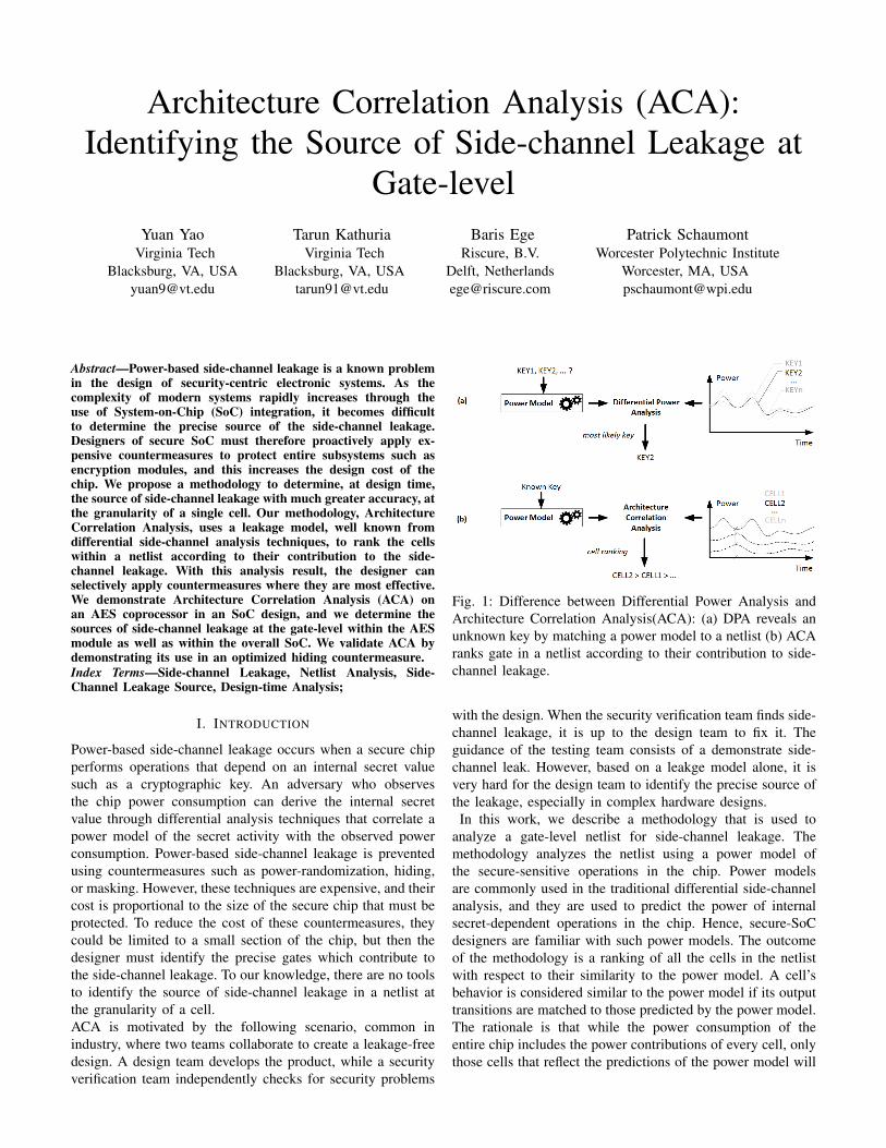
Fig. 1: Difference between Differential Power Analysis andArchitecture Correlation Analysis(ACA): (a) DPA reveals anunknown key by matching a power model to a netlist (b) ACAranks gate in a netlist according to their contribution to side-channel leakage.
with the design. When the security verification team finds side-channel leakage, it is up to the design team to fix it. Theguidance of the testing team consists of a demonstrate side-channel leak. However, based on a leakge model alone, it isvery hard for the design team to identify the precise source ofthe leakage, especially in complex hardware designs.
In this work, we describe a methodology that is used toanalyze a gate-level netlist for side-channel leakage. Themethodology analyzes the netlist using a power model ofthe secure-sensitive operations in the chip. Power modelsare commonly used in the traditional differential side-channelanalysis, and they are used to predict the power of internalsecret-dependent operations in the chip. Hence, secure-SoCdesigners are familiar with such power models. The outcomeof the methodology is a ranking of all the cells in the netlistwith respect to their similarity to the power model. A cell’sbehavior is considered similar to the power model if its outputtransitions are matched to those predicted by the power model.The rationale is that while the power consumption of theentire chip includes the power contributions of every cell, onlythose cells that reflect the predictions of the power model will
contribute to side-channel leakage.The ranking is numerically expressed using the Leakage Im-pact Factor (LIF), a gate-level metric to express side-channelleakage. The higher the LIF, the more a cell contributes topower-side-channel leakage. With the LIF, the designer canthen decide what cells to protect using a countermeasure.While ACA in itself is not a countermeasure, it enables acritical step in applying countermeasures more efficiently.Figure 1 clarifies the difference between Architecture Cor-relation Analysis (ACA) and traditional side-channel anal-ysis. Traditional (differential) side-channel analysis (Figure1a) aims to reveal a secret, such as a cryptographic key. Apower model, dependent on a secret key, is compared withthe measured (or simulated) power trace obtained from a chip.The best-matching power model reveals the most likely key.On the other hand, our proposed ACA (Figure 1b) ranks cellsin a netlist according to their contribution to side-channelleakage. The ranking is determined by comparing the powerconsumption from individual gates with a power model thatuses a known key, and a closer similarity between cell powerand power model leads to a higher ranking. The gate-levelpower consumption is obtained using power simulation. Thus,ACA is not a side-channel analysis technique, but rather anetlist analysis technique.In this contribution, we introduce the ACA methodologyand we apply it to a System-on-Chip Design. We analyzeindividual modules (such as an AES coprocessor) as well assystem-level interconnect. ACA has two different use-modes.First, when a known source of side-channel leakage suchas an unprotected hardware cipher is analyzed, ACA willconfirm the source of side-channel leakage at the granularityof a single cell. Second, with a known side-channel leakagepower model, such as the transfer of a secret value, ACA willidentify every cell that contributes to the side-channel leakagepredicted by the power model. In both cases, our experimentson practical SoC design show that only a small number ofcells are significantly contributing to side-channel leakage.The outline of the paper is as follows. In the next section, wediscuss related work. Section III describes the ACA method-ology. We demonstrate two practical case studies. Section IVintroduces the experimental setup. Section V applies ACA tothe analysis of a coprocessor. Section VI applies ACA to theanalysis of an SoC bus transfer. Section VII illustrates theeffectiveness of ACA by using it to implement an optimizedhiding countermeasure. In Section VIII, we provide severaldiscussions about the relevant issues of ACA. By selectivelyprotecting the cells flagged by ACA as sources of side-channelleakage, we show that the side-channel leakage in the overallsystem can be reduced significantly. We then conclude thepaper.
II. RELATED WORK
Many authors have investigated the problem of predicting side-channel leakage using circuit simulation techniques, includingsimulation of EM-leakage [1], transistor (SPICE-level) powerconsumption [2], gate-level (PrimeTime Px-level) power con-sumption [3], or profiled modeling [4]. These efforts aim atreproducing side-channel leakage at design time, so that a
side-channel attack can be simulated and countermeasures canbe tested. Simulation-based side-channel leakage assessmentmethods make a trade-off between simulation speed andaccuracy. Such simulations result in noiseless power estimates,thereby significantly reducing the number of traces requiredfor a side-channel attack. Nevertheless, none of these methodsinvestigates the ranking of design components according toside-channel leakage, which is the main contribution of ACA.A second related work topic is on how designers can usedesign data, at any level of abstraction, to identify the sourceof side-channel leakage. Information flow tracking techniquesautomatically identify causal dependencies between the dif-ferent parts of a design, and therefore these techniques cananalyze the dependencies between a sensitive or secret inputand an observable design output. At the register-transfer level,SecVerilog [5] analyzes hardware information flow to detecttiming-based channels. At the gate-level, GLIFT [6] simi-larly detects timing-dependent information leaks. However,information-flow based mechanisms cannot express power-based side-channel leakage. RTL-PSC [7] describes a design-time side-channel leakage assessment methodology at theRegister-Transfer level. The authors identify side-channel leak-age at the module-level, when a design is still at RTL.However, RTL-PSC ignores low level effects such as glitches,a known source of side-channel leakage [8], as well as theeffects of physical placement and routing. Other authors haveproposed empirical methods for locating side-channel leakagein a prototype implementation. By systematically scanning achip and establishing a cartography of EM-based side-channelleakage [9], the areas of the chip with the most side-channelleakage can be found. However, the accuracy of these methodsis very coarse and they are unable to identify side-channelleakage at the cell level.Karna [10] is another approach to design-time side-channelleakage assessment which operates at the layout level. Theauthors partition a chip spatially in small cells, and determinea TVLA leakage metric for each area. This reveals the leakagespecific to local area of the chip. TVLA is a generic leakagemetric with known caveats, the most important being that itdoes not confirm that a side-channel attack exists. Second,the resolution of Karna is limited by the layout area overwhich TVLA is computed, which typically will still containmany gates. As previous authors have repeatedly shown, side-channel leaks can often be attributed to a single gate [11],which may trigger the use of specific gate-level countermea-sures. For this reason, we think it remains imperative toidentify the side-channel leakage contributed by a single gate.
III. ACA METHODOLOGY
In this section, we describe the ACA methodology. We mo-tivate principal design choices, recall preliminaries on side-channel leakage models, and introduce the ACA method tocompute the leakage impact factor of a gate.We motivate two of our principal design choices. First, todetect leakage, ACA relies on a leakage model, and it is upto the designer to select the right leakage model. However,these models are commonly known. Internal and externalsecurity testing labs estimate the strength of an implementation
using state of the art side-channel attacks either on silicon orthrough simulations. Such attacks typically use leakage modelsand therefore the designer can obtain the knowledge of the‘right’ leakage model as a result of the testing effort. Weacknowledge that statistical detection methods, such as TVLA,can demonstrate the presence of sensitive variables in a powertrace and that they avoid the difficulty of choosing a leakagemodel. However, TVLA comes with its own risks such as falsepositives [12]. This means that a positive leakage test result forTVLA does not imply that an attack exists. Second, ACA usesgate-level power modeling on post-synthesis or post-layoutnetlists. Power modeling at the gate-level abstraction levelstrikes a balance between simulation efficiency and accuracy. Itis applicable to the complete chip, while still correctly charac-terizing sub-cycle-level power effects. In contrast, RTL powermodeling or toggle-counting misses many of the importantelectrical effects in side-channel leakage, and transistor-levelpower modeling is too complex to achieve at chip-level overextended periods of time.
A. Leakage model
The leakage model, in the context of power-based side-channelanalysis, is an estimate for the information leakage incurredthrough power consumption variations. The leakage model Lis a function computed over a secret intermediate variableV . The objective of side-channel analysis is to reveal thevalue of V through many observations of the measured powerconsumption and correlating those observations with L(V ).Popular choices for L(V ) are the Hamming Weight or theHamming Distance on V ; the Hamming Weight reflects value-based power leakage in CMOS, while the Hamming Distancereflects distance-based power leakage in CMOS.The objective of ACA is to identify, within a gate-levelnetlist, those cells that realize L(V ). Naturally, there aremany possible choices for the leakage function, and ACAmakes the assumption that the designer is able to provideL(V ). If the algorithm and implementation are known, such aleakage function can always be found. For example, a commonchoice for L(V ) for AES hardware implementations is theHamming Distance between the state of different rounds. ForAES software implementations, the Hamming Weight of oneor a few bytes of the AES state is typically used.However, V does not have to be related to a cryptographickey, and any sensitive value processed in a design could beanalyzed. For example, ACA can be used to study bus transferoperations in an SoC. In that case, V is a sensitive valuetransferred over the bus, and L(V ) is the Hamming weightof the value. The Hamming weight reflects the pre-chargednature of a shared bus [13].
B. Computing the Leakage Impact Factor
The purpose of ACA is to define the Leakage Impact Factor(LIF) for every cell in a design. The LIF is a dimensionlessnumber that expresses the contribution of the cell’s powerconsumption to the side-channel leakage of a design, and ahigher LIF indicates a higher contribution. We summarize thesteps of LIF computation. The input of ACA consists of anetlist to be analyzed, a secure asset V , a leakage model L(V ),
TABLE I: Pearson Correlation Threshold Levels as a functionConfidence
Confidence Interval n=600 n=1000 n=200099% ±0.105 ±0.081 ±0.05895% ±0.080 ±0.062 ±0.04490% ±0.067 ±0.052 ±0.037
and a set of stimuli that exercise the netlist and the secure asset.We first identify the Leakage Time Interval (LTI), the timeinterval over which we want to obtain LIF. Next, we computefor every cell i in the design an architecture correlation factorCi as well as the average normalized power consumption Pi
PT.
Finally, we obtain the gate LIF as the product of these two.We discuss each of these steps in detail.a) Selecting the Leakage Time Interval:The first step of ACA is to narrow down the time window overwhich the Leakage Impact Factors are computed. The rationaleis that we want to determine the LIF over an interval duringwhich the leakage model L(V ) is valid and during which side-channel leakage may occur. We therefore narrow the searchwindow to the Leakage Time Interval using power correlation.We use simulated system-level power traces P and correlatethem with the traces from the leakage model L(V ). We thencompute the correlation ρ as
ρL(V ),t =cov(L(V ), P (t))
σL(V )σP(1)
where:
cov = the covarianceσL(V ) = the standard deviation of L(V )σP = the standard deviation of P
The Leakage Time Interval is defined as the time window(s)for which
ρL(V ),t > ρthreshold (2)
The threshold level ρthreshold is based on the designer’sdefinition of a distinguishable correlation peak. We can usethe Pearson Correlation Confidence Interval to define boundsfor ρthreshold. Table I illustrates several choices for ρthreshold.Under the hypothesis that the true ρ is zero, the table showsconfidence intervals in function of the number of traces (n)and the confidence level. Hence, if the observed ρ falls outsideof the confidence interval then we reject the hypothesis andconclude that the design shows leakage.Because we are computing ρ in a noiseless, controlled envi-ronment with full knowledge of the secure asset, we can findsharp correlation peaks with a limited number of traces.b) Architecture Correlation:Within the Leakage Time Interval, we next perform the archi-tecture correlation as follows. First, we obtain a toggle tracefrom a gate-level simulation of the design. A toggle trace Ki
records the activity of each net i (driven by cell i) using thediscrete values −1 and +1. If a cell has multiple outputs, thenwe compute the architecture correlation and leakage impactfactor for each output separately. For each time stamp t inthe simulation, a toggle trace for net i has the value −1 ifthe net does not change value, and it has the value +1 if the
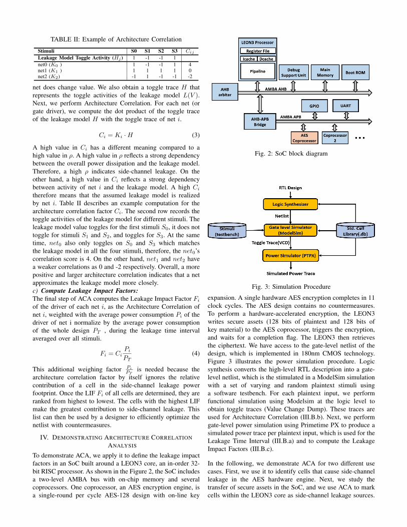
TABLE II: Example of Architecture Correlation
Stimuli S0 S1 S2 S3 Cij
Leakage Model Toggle Activity (Hj ) 1 -1 -1 1net0 (K0 ) 1 -1 -1 1 4net1 (K1 ) 1 1 1 1 0net2 (K2) -1 1 -1 -1 -2
net does change value. We also obtain a toggle trace H thatrepresents the toggle activities of the leakage model L(V ).Next, we perform Architecture Correlation. For each net (orgate driver), we compute the dot product of the toggle traceof the leakage model H with the toggle trace of net i.
Ci = Ki ·H (3)
A high value in Ci has a different meaning compared to ahigh value in ρ. A high value in ρ reflects a strong dependencybetween the overall power dissipation and the leakage model.Therefore, a high ρ indicates side-channel leakage. On theother hand, a high value in Ci reflects a strong dependencybetween activity of net i and the leakage model. A high Ci
therefore means that the assumed leakage model is realizedby net i. Table II describes an example computation for thearchitecture correlation factor Ci. The second row records thetoggle activities of the leakage model for different stimuli. Theleakage model value toggles for the first stimuli S0, it does nottoggle for stimuli S1 and S2, and toggles for S3. At the sametime, net0 also only toggles on S0 and S3 which matchesthe leakage model in all the four stimuli, therefore, the net0’scorrelation score is 4. On the other hand, net1 and net2 havea weaker correlations as 0 and -2 respectively. Overall, a morepositive and larger architecture correlation indicates that a netapproximates the leakage model more closely.c) Compute Leakage Impact Factors:The final step of ACA computes the Leakage Impact Factor Fi
of the driver of each net i, as the Architecture Correlation ofnet i, weighted with the average power consumption Pi of thedriver of net i normalize by the average power consumptionof the whole design PT , during the leakage time intervalaveraged over all stimuli.
Fi = CiPi
PT(4)
This additional weighing factor Pi
PTis needed because the
architecture correlation factor by itself ignores the relativecontribution of a cell in the side-channel leakage powerfootprint. Once the LIF Fi of all cells are determined, they areranked from highest to lowest. The cells with the highest LIFmake the greatest contribution to side-channel leakage. Thislist can then be used by a designer to efficiently optimize thenetlist with countermeasures.
IV. DEMONSTRATING ARCHITECTURE CORRELATIONANALYSIS
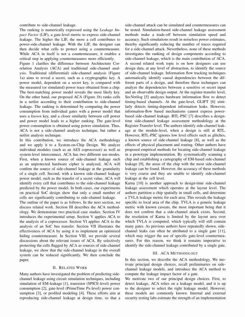
To demonstrate ACA, we apply it to define the leakage impactfactors in an SoC built around a LEON3 core, an in-order 32-bit RISC processor. As shown in the Figure 2, the SoC includesa two-level AMBA bus with on-chip memory and severalcoprocessors. One coprocessor, an AES encryption engine, isa single-round per cycle AES-128 design with on-line key
Fig. 2: SoC block diagram
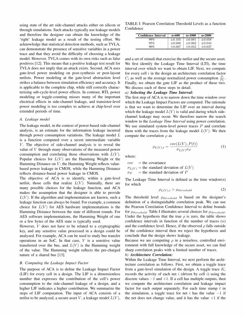
Fig. 3: Simulation Procedure
expansion. A single hardware AES encryption completes in 11clock cycles. The AES design contains no countermeasures.To perform a hardware-accelerated encryption, the LEON3writes secure assets (128 bits of plaintext and 128 bits ofkey material) to the AES coprocessor, triggers the encryption,and waits for a completion flag. The LEON3 then retrievesthe ciphertext. We have access to the gate-level netlist of thedesign, which is implemented in 180nm CMOS technology.Figure 3 illustrates the power simulation procedure. Logicsynthesis converts the high-level RTL description into a gate-level netlist, which is the stimulated in a ModelSim simulationwith a set of varying and random plaintext stimuli usinga software testbench. For each plaintext input, we performfunctional simulation using Modelsim at the logic level toobtain toggle traces (Value Change Dump). These traces areused for Architecture Correlation (III.B.b). Next, we performgate-level power simulation using Primetime PX to produce asimulated power trace per plaintext input, which is used for theLeakage Time Interval (III.B.a) and to compute the LeakageImpact Factors (III.B.c).
In the following, we demonstrate ACA for two different usecases. First, we use it to identify cells that cause side-channelleakage in the AES hardware engine. Next, we study thetransfer of secure assets in the SoC, and we use ACA to markcells within the LEON3 core as side-channel leakage sources.
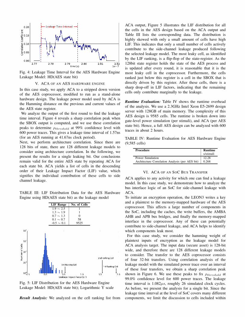
Fig. 4: Leakage Time Interval for the AES Hardware EngineLeakage Model: HD(AES state bit)
V. ACA OF AN AES HARDWARE ENGINE
In this case study, we apply ACA to a stripped down versionof the AES coprocessor, modified to run as a stand-alonehardware design. The leakage power model used by ACA isthe Hamming distance on the previous and current values ofthe AES state register.We analyze the output of the first round to find the leakage
time interval. Figure 4 reveals a sharp correlation peak whenthe SBOX output is computed, and we use these correlationpeaks to determine ρthreshold at 99% confidence level with600 power traces. This gives a leakage time interval of 1.57ns(for an AES running at 41.67ns clock period).Next, we perform architecture correlation. Since there are128 bits of state, there are 128 different leakage models toconsider using architecture correlation. In the following, wepresent the results for a single leaking bit. Our conclusionsremain valid for the entire AES state by repeating ACA foreach state bit. ACA yields a list of cells in the descendingorder of their Leakage Impact Factor (LIF) value, whichsignifies the individual contribution of these cells to sidechannel leakage.
TABLE III: LIF Distribution Data for the AES HardwareEngine using HD(AES state bit) as the leakage model
LIF Range No. of Cells1.9 ∼ 2.5 11.3 ∼ 1.9 10.7 ∼ 1.3 00.1 ∼ 0.7 58-0.5 ∼ 0.1 9525
Fig. 5: LIF Distribution for the AES Hardware EngineLeakage Model: HD(AES state bit); Logarithmic Y scale
Result Analysis: We analyzed on the cell ranking list from
ACA output, Figure 5 illustrates the LIF distribution for allthe cells in the AES design based on the ACA output andTable III lists the corresponding data. The distribution ishighly skewed with only a small amount of cells have highLIF. This indicates that only a small number of cells activelycontribute to the side-channel leakage produced followingthe selected leakage model. The most leaky cell, as identifiedby the LIF ranking, is a flip-flop of the state-register. As the128bit state register holds the state of the AES process andis updated after every round, it is reasonable that it is themost leaky cell in the coprocessor. Furthermore, the cellsranked just below this register is a cell in the SBOX that isdirectly driven by this register. After these cells, there is asharp drop-off in LIF factors, indicating that the remainingcells only contribute marginally to the leakage.
Runtime Evaluation: Table IV shows the runtime overheadof the analysis. We use a 2.3GHz Intel Xeon E5-2699 designserver with 128GB of main memory. The complexity of thisAES design is 9585 cells. The runtime is broken down intogate-level power simulation (per stimuli), and ACA (per AESstate bit). Hence, a full AES design can be analyzed with 600traces in about 2 hours.
TABLE IV: Runtime Evaluation for AES Hardware Engine(9,585 cells)
Procedure Runtimes/stimuli
Power Simulation 12.28Architecture Correlation Analysis (per AES bit) 0.268
VI. ACA OF AN SOC BUS TRANSFER
ACA applies to any activity for which one can find a leakagemodel. In this case study, we demonstrate how to analyze thebus interface logic of an SoC for side-channel leakage withACA.To initiate an encryption operation, the LEON3 writes a keyand a plaintext to the memory-mapped hardware of the AEScoprocessor. This affects a large number of components inthe SoC, including the caches, the write buffers, the AMBAAHB and APB bus bridges, and finally the memory-mappedinterface in the coprocessor. Any of these can potentiallycontribute to side-channel leakage, and ACA helps to identifywhich components leak most.
For this case study, we consider the hamming weight ofplaintext inputs of encryption as the leakage model forACA analysis target. The input data (secure asset) is 128-bitwide, and therefore there are 128 different leakage modelsto consider. The transfer to the AES coprocessor consistsof four 32-bit transfers. Using correlation analysis of theleakage model with the simulated power trace over an intervalof these four transfers, we obtain a sharp correlation peakshown in Figure 6. We use these peaks to fix ρthreshold at99.0% confidence level for 600 power traces. The leakagetime interval is 1.082µs, roughly 26 simulated clock cycles.As before, we present the analysis for a single bit. Since theleakage time interval at the level of SoC covers many differentcomponents, we limit the discussion to cells included within
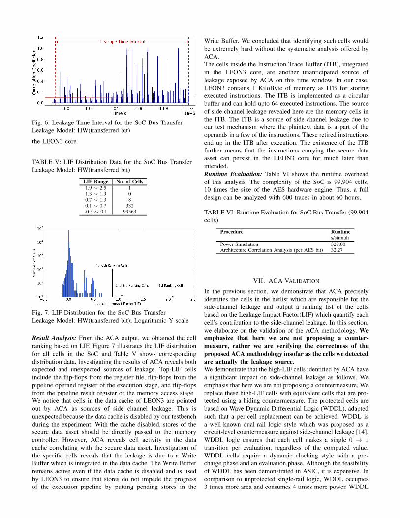
Fig. 6: Leakage Time Interval for the SoC Bus TransferLeakage Model: HW(transferred bit)
the LEON3 core.
TABLE V: LIF Distribution Data for the SoC Bus TransferLeakage Model: HW(transferred bit)
LIF Range No. of Cells1.9 ∼ 2.5 11.3 ∼ 1.9 00.7 ∼ 1.3 80.1 ∼ 0.7 332-0.5 ∼ 0.1 99563
Fig. 7: LIF Distribution for the SoC Bus TransferLeakage Model: HW(transferred bit); Logarithmic Y scale
Result Analysis: From the ACA output, we obtained the cellranking based on LIF. Figure 7 illustrates the LIF distributionfor all cells in the SoC and Table V shows correspondingdistribution data. Investigating the results of ACA reveals bothexpected and unexpected sources of leakage. Top-LIF cellsinclude the flip-flops from the register file, flip-flops from thepipeline operand register of the execution stage, and flip-flopsfrom the pipeline result register of the memory access stage.We notice that cells in the data cache of LEON3 are pointedout by ACA as sources of side channel leakage. This isunexpected because the data cache is disabled by our testbenchduring the experiment. With the cache disabled, stores of thesecure data asset should be directly passed to the memorycontroller. However, ACA reveals cell activity in the datacache correlating with the secure data asset. Investigation ofthe specific cells reveals that the leakage is due to a WriteBuffer which is integrated in the data cache. The Write Bufferremains active even if the data cache is disabled and is usedby LEON3 to ensure that stores do not impede the progressof the execution pipeline by putting pending stores in the
Write Buffer. We concluded that identifying such cells wouldbe extremely hard without the systematic analysis offered byACA.The cells inside the Instruction Trace Buffer (ITB), integratedin the LEON3 core, are another unanticipated source ofleakage exposed by ACA on this time window. In our case,LEON3 contains 1 KiloByte of memory as ITB for storingexecuted instructions. The ITB is implemented as a circularbuffer and can hold upto 64 executed instructions. The sourceof side channel leakage revealed here are the memory cells inthe ITB. The ITB is a source of side-channel leakage due toour test mechanism where the plaintext data is a part of theoperands in a few of the instructions. These retired instructionsend up in the ITB after execution. The existence of the ITBfurther means that the instructions carrying the secure dataasset can persist in the LEON3 core for much later thanintended.Runtime Evaluation: Table VI shows the runtime overheadof this analysis. The complexity of the SoC is 99,904 cells,10 times the size of the AES hardware engine. Thus, a fulldesign can be analyzed with 600 traces in about 60 hours.
TABLE VI: Runtime Evaluation for SoC Bus Transfer (99,904cells)
Procedure Runtimes/stimuli
Power Simulation 329.00Architecture Correlation Analysis (per AES bit) 32.27
VII. ACA VALIDATION
In the previous section, we demonstrate that ACA preciselyidentifies the cells in the netlist which are responsible for theside-channel leakage and output a ranking list of the cellsbased on the Leakage Impact Factor(LIF) which quantify eachcell’s contribution to the side-channel leakage. In this section,we elaborate on the validation of the ACA methodology. Weemphasize that here we are not proposing a counter-measure, rather we are verifying the correctness of theproposed ACA methodology insofar as the cells we detectedare actually the leakage source.We demonstrate that the high-LIF cells identified by ACA havea significant impact on side-channel leakage as follows. Weemphasis that here we are not proposing a countermeasure, Wereplace these high-LIF cells with equivalent cells that are pro-tected using a hiding countermeasure. The protected cells arebased on Wave Dynamic Differential Logic (WDDL), adaptedsuch that a per-cell replacement can be achieved. WDDL isa well-known dual-rail logic style which was proposed as acircuit-level countermeasure against side-channel leakage [14].WDDL logic ensures that each cell makes a single 0 → 1transition per evaluation, regardless of the computed value.WDDL cells require a dynamic clocking style with a pre-charge phase and an evaluation phase. Although the feasibilityof WDDL has been demonstrated in ASIC, it is expensive. Incomparison to unprotected single-rail logic, WDDL occupies3 times more area and consumes 4 times more power. WDDL
KEY1KEY2
KEYn...
Power Model
Time
Power
Time
PowerGATE1GATE2
GATEn...
KEY2
Power Model
GATE2 > GATE1 > ...
Differential PowerAnalysis
ArchitectureCorrelationAnalysis
most likely key
gate ranking
KEY1, KEY2, ... ?
Known Key
(a)
(b)
D QAB Y
D Q
D Q
D Q
D Q
Y
AB
precharge
clk2 clk2
clk2 clk2
precharge
clk2clk
clk
(a)
(b)
(c)
Top‐LIF net
Fig. 8: Selective-replacement WDDL (a) Original Circuit (b)Transformed Circuit (c) Clocking.
is therefore a costly technique to apply chip-wide. Whenwe replace only the high-LIF cells with WDDL versions,the impact on area will be much smaller, while still havinga significant impact on the side-channel leakage. We willfirst explain our countermeasure methodology to implementWDDL on a cell-replacement basis. Next, we evaluate thecost and impact of this countermeasure on the side-channelleakage of the AES hardware.
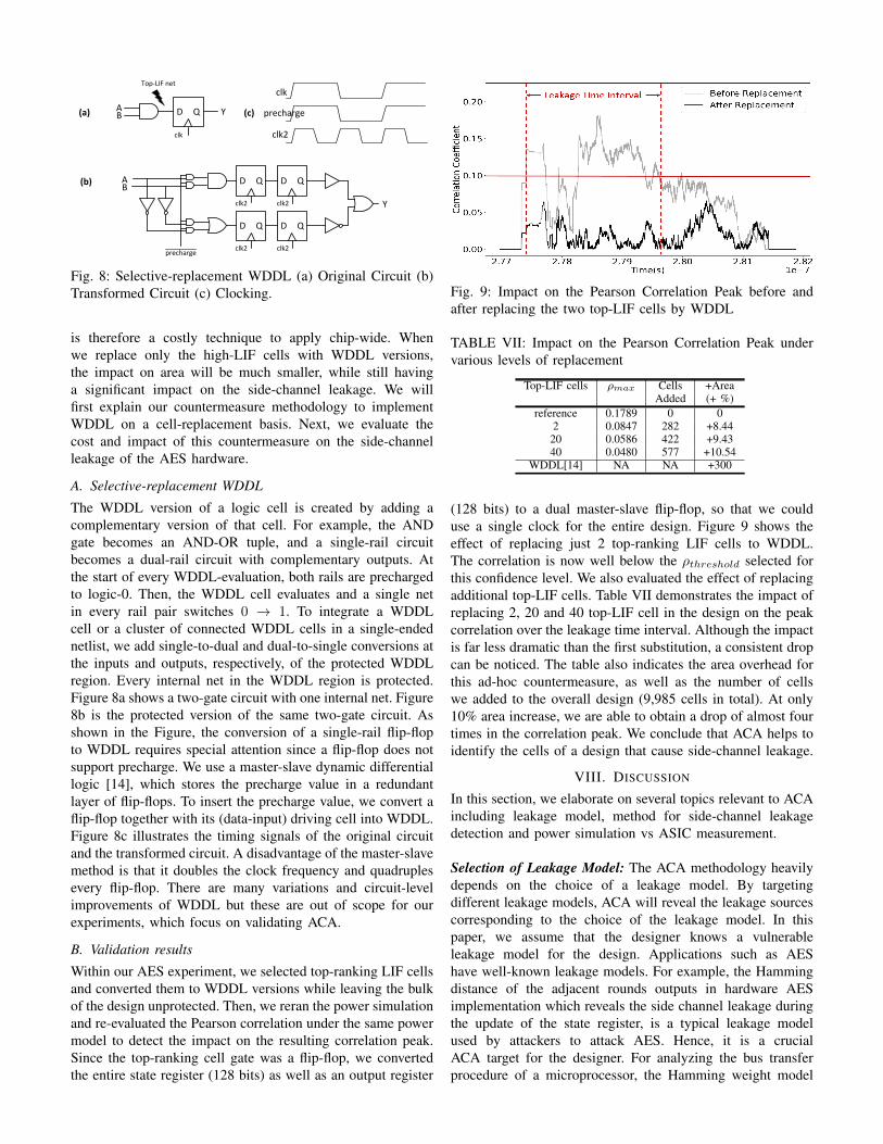
A. Selective-replacement WDDL
The WDDL version of a logic cell is created by adding acomplementary version of that cell. For example, the ANDgate becomes an AND-OR tuple, and a single-rail circuitbecomes a dual-rail circuit with complementary outputs. Atthe start of every WDDL-evaluation, both rails are prechargedto logic-0. Then, the WDDL cell evaluates and a single netin every rail pair switches 0 → 1. To integrate a WDDLcell or a cluster of connected WDDL cells in a single-endednetlist, we add single-to-dual and dual-to-single conversions atthe inputs and outputs, respectively, of the protected WDDLregion. Every internal net in the WDDL region is protected.Figure 8a shows a two-gate circuit with one internal net. Figure8b is the protected version of the same two-gate circuit. Asshown in the Figure, the conversion of a single-rail flip-flopto WDDL requires special attention since a flip-flop does notsupport precharge. We use a master-slave dynamic differentiallogic [14], which stores the precharge value in a redundantlayer of flip-flops. To insert the precharge value, we convert aflip-flop together with its (data-input) driving cell into WDDL.Figure 8c illustrates the timing signals of the original circuitand the transformed circuit. A disadvantage of the master-slavemethod is that it doubles the clock frequency and quadruplesevery flip-flop. There are many variations and circuit-levelimprovements of WDDL but these are out of scope for ourexperiments, which focus on validating ACA.
B. Validation results
Within our AES experiment, we selected top-ranking LIF cellsand converted them to WDDL versions while leaving the bulkof the design unprotected. Then, we reran the power simulationand re-evaluated the Pearson correlation under the same powermodel to detect the impact on the resulting correlation peak.Since the top-ranking cell gate was a flip-flop, we convertedthe entire state register (128 bits) as well as an output register
Fig. 9: Impact on the Pearson Correlation Peak before andafter replacing the two top-LIF cells by WDDL
TABLE VII: Impact on the Pearson Correlation Peak undervarious levels of replacement
Top-LIF cells ρmax Cells +AreaAdded (+ %)
reference 0.1789 0 02 0.0847 282 +8.44
20 0.0586 422 +9.4340 0.0480 577 +10.54
WDDL[14] NA NA +300
(128 bits) to a dual master-slave flip-flop, so that we coulduse a single clock for the entire design. Figure 9 shows theeffect of replacing just 2 top-ranking LIF cells to WDDL.The correlation is now well below the ρthreshold selected forthis confidence level. We also evaluated the effect of replacingadditional top-LIF cells. Table VII demonstrates the impact ofreplacing 2, 20 and 40 top-LIF cell in the design on the peakcorrelation over the leakage time interval. Although the impactis far less dramatic than the first substitution, a consistent dropcan be noticed. The table also indicates the area overhead forthis ad-hoc countermeasure, as well as the number of cellswe added to the overall design (9,985 cells in total). At only10% area increase, we are able to obtain a drop of almost fourtimes in the correlation peak. We conclude that ACA helps toidentify the cells of a design that cause side-channel leakage.
VIII. DISCUSSION
In this section, we elaborate on several topics relevant to ACAincluding leakage model, method for side-channel leakagedetection and power simulation vs ASIC measurement.
Selection of Leakage Model: The ACA methodology heavilydepends on the choice of a leakage model. By targetingdifferent leakage models, ACA will reveal the leakage sourcescorresponding to the choice of the leakage model. In thispaper, we assume that the designer knows a vulnerableleakage model for the design. Applications such as AEShave well-known leakage models. For example, the Hammingdistance of the adjacent rounds outputs in hardware AESimplementation which reveals the side channel leakage duringthe update of the state register, is a typical leakage modelused by attackers to attack AES. Hence, it is a crucialACA target for the designer. For analyzing the bus transferprocedure of a microprocessor, the Hamming weight model
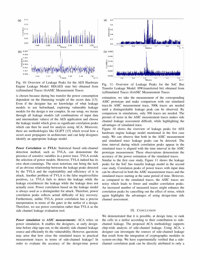
Fig. 10: Overview of Leakage Peaks for the AES HardwareEngine Leakage Model: HD(AES state bit) obtained from(a)Simulated Traces (b)ASIC Measurement Traces
is chosen because during bus transfer the power consumptiondependent on the Hamming weight of the secret data [13].Even if the designer has no knowledge of what leakagemodels to use beforehand, exploring vulnerable leakagemodels for the design is not complex. In our setup, we iteratethrough all leakage models (all combinations of input dataand intermediate values) of the AES application and choosethe leakage model which gives us significant correlation peakswhich can then be used for analysis using ACA. Moreover,there are methodologies like GLIFT [15] which reveal how asecret asset propagates in architecture and can help designersidentify an appropriate leakage model.
Power Correlation vs TVLA: Statistical based side-channeldetection method, such as TVLA, can demonstrate thepresence of sensitive variables in a power trace. TVLA avoidsthe selection of power models. However, TVLA indeed has itsown short-commings. The most notorious one being the lackof an obvious relationship between the leakage peaks detectedby the TVLA and the exploitability and efficiency of it inattack. Another problem of TVLA is the false negatives/falsepositives, i.e. TVLA fails to detect the leakage while theleakage exist/detects the leakage while the leakage does notactually exist. Power correlation based on the leakage modelis always used as a distinguisher for attack. Therefore, powercorrelation peaks reflects actual difficulty of key recovery.Furthermore, unlike TVLA, power correlation has a preciseinterpretation in terms of the gates in the netlist of a design.Therefore, we use power correlation rather than TVLA as theside channel leakage evaluation tool.
Power simulation vs ASIC measurements: ACA relies onpower simulation. It enables the designers, at early design-time before chip tape-out, to the identify side channel leakagesource and efficiently fix the vulnerability. However, questionsmay arise that how close the simulated traces to practicalmeasurement traces in terms of side-channel leakage? Inorder to evaluate the accuracy of the design-time power
Fig. 11: Overview of Leakage Peaks for the SoC BusTransfer Leakage Model: HW(transferred bit) obtained from(a)Simulated Traces (b)ASIC Measurement Traces
estimation, we take the measurement of the correspondingASIC prototype and make comparison with our simulatedtrace.In ASIC measurement trace, 500k traces are neededuntil a distinguishable leakage peak can be observed. Bycomparison in simulations, only 500 traces are needed. Thepresnet of noise in the ASIC measurement traces makes sidechannel leakage assessment difficult, while highlighting theadvantages of simulated trace.Figure 10 shows the overview of leakage peaks for AEShardware engine leakage model mentioned in the first casestudy. We can observe that both in the ASIC measurementand simulated trace leakage peaks can be detected. Thetime interval during which correlation peaks appear in thesimulated trace is aligned with the time interval in the ASICprototype measurement. These observations demonstrate theaccuracy of the power estimation of the simulated traces.Similar to the first case study, Figure 11 shows the leakagepeaks for the SoC bus transfer leakage model in the secondcase study. Correlation peaks of power traces with input datacan be observed in both the ASIC measurement traces and thesimulated traces starting at the same period of time. However,as compared to the simulated traces, the ASIC traces arenoisy which leads to fewer and smaller correlation peaks.An increased number of measured traces might enhance thecorrelation peaks by cancelling out the effect of noise, whichagain highlights the advantages of using design-time sidechannel assessment.
IX. CONCLUSION
We demonstrated that it is possible, at design time, to rankthe cells in a netlist according to their contribution to side-channel leakage. The proposed ACA methodology supportschip-wide analysis of side-channel leakage. Using ACA, adesigner can investigate the sources of side-channel leakagethat result from the integration of cryptographic modules insystem-on-chip. We have experimentally verified that a side-channel correlation peak can be directly attributed to only a
minority of the cells in a netlist. A potential use of ACA istherefore to fix side-channel leakage by selective replacementof cells in the netlist. This can be done iteratively, and it opensup a new perspective for the development of side-channelcountermeasures. Indeed, traditional countermeasures work inan all-or-nothing approach, treating a cryptographic moduleas a black box and protecting all of its cells. This is notonly expensive, it also ignores residual side-channel leakagethat stems from the integration of the module in a system-on-chip. The ACA methodology fits in a design flow thatcomprehensively optimizes the security, timing, and area ofa design.
X. ACKNOWLEDGEMENT
This research was supported in part by National ScienceFoundation Award 1617203. The authors would like to thankanonymous reviewers for their valuable feedback.
REFERENCES
[1] Amit Kumar, Cody Scarborough, Ali Yilmaz, and Michael Orshansky,“Efficient simulation of EM side-channel attack resilience”, in 2017IEEE/ACM International Conference on Computer-Aided Design, IC-CAD 2017, Irvine, CA, USA, November 13-16, 2017, 2017, pp. 123–130.
[2] Francesco Regazzoni, Stephane Badel, Thomas Eisenbarth, JohannGroßschadl, Axel Poschmann, Zeynep Toprak Deniz, Marco Mac-chetti, Laura Pozzi, Christof Paar, Yusuf Leblebici, and Paolo Ienne,“A simulation-based methodology for evaluating the dpa-resistance ofcryptographic functional units with application to CMOS and MCMLtechnologies”, in Proceedings of the 2007 International Conference onEmbedded Computer Systems: Architectures, Modeling and Simulation(IC-SAMOS 2007), Samos, Greece, July 16-19, 2007, 2007, pp. 209–214.
[3] Danilo Sijacic, Josep Balasch, Bohan Yang, Santosh Ghosh, and IngridVerbauwhede, “Towards efficient and automated side channel evalua-tions at design time”, in PROOFS 2018, 7th International Workshopon Security Proofs for Embedded Systems, colocated with CHES 2018,Amsterdam, The Netherlands, September 13, 2018, 2018, pp. 16–31.
[4] Nicolas Debande, Mael Berthier, Yves Bocktaels, and Thanh-Ha Le,“Profiled model based power simulator for side channel evaluation”,IACR Cryptology ePrint Archive, vol. 2012, pp. 703, 2012.
[5] Danfeng Zhang, Aslan Askarov, and Andrew C. Myers, “Language-based control and mitigation of timing channels”, SIGPLAN Not., vol.47, no. 6, pp. 99–110, June 2012.
[6] Jason Oberg, Sarah Meiklejohn, Timothy Sherwood, and Ryan Kastner,“Leveraging gate-level properties to identify hardware timing channels”,IEEE Trans. on CAD of Integrated Circuits and Systems, vol. 33, no. 9,pp. 1288–1301, 2014.
[7] Miao Tony He, Jungmin Park, Adib Nahiyan, Apostol Vassilev, YierJin, and Mark Tehranipoor, “RTL-PSC: automated power side-channelleakage assessment at register-transfer level”, in 37th IEEE VLSI TestSymposium, VTS 2019, Monterey, CA, USA, April 23-25, 2019, 2019,pp. 1–6.
[8] Stefan Mangard and Kai Schramm, “Pinpointing the side-channelleakage of masked AES hardware implementations”, in CryptographicHardware and Embedded Systems - CHES 2006, 8th InternationalWorkshop, Yokohama, Japan, October 10-13, 2006, Proceedings, 2006,pp. 76–90.
[9] Laurent Sauvage, Sylvain Guilley, Florent Flament, Jean-Luc Danger,and Yves Mathieu, “Blind cartography for side channel attacks:Cross-correlation cartography”, Int. J. Reconfig. Comp., vol. 2012, pp.360242:1–360242:9, 2012.
[10] Patanjali SLPSK, Prasanna Karthik Vairam, Chester Rebeiro, and Ka-makoti Veezhinathan, “Karna: A gate-sizing based security aware edaflow for improved power side-channel attack protection”, in Proceedingsof the International Conference on Computer-Aided Design, ICCAD2019, Westminster, CO, USA, November 04-07, 2019.
[11] Stefan Mangard, Thomas Popp, and Berndt M Gammel, “Side-channelleakage of masked cmos gates”, in Cryptographers’ Track at the RSAConference. Springer, 2005, pp. 351–365.
[12] Carolyn Whitnall and Elisabeth Oswald, “A cautionary note regardingthe usage of leakage detection tests in security evaluation”, IACRCryptology ePrint Archive, vol. 2019, pp. 703, 2019.
[13] Eric Peeters, Francois-Xavier Standaert, and Jean-Jacques Quisquater,“Power and electromagnetic analysis: Improved model, consequencesand comparisons”, Integration, the VLSI journal, vol. 40, no. 1, pp.52–60, 2007.
[14] Kris Tiri and Ingrid Verbauwhede, “A logic level design methodologyfor a secure dpa resistant asic or fpga implementation”, in ProceedingsDesign, Automation and Test in Europe Conference and Exhibition.IEEE, 2004, vol. 1, pp. 246–251.
[15] Jason Oberg, Sarah Meiklejohn, Timothy Sherwood, and Ryan Kastner,“Leveraging gate-level properties to identify hardware timing channels”,IEEE Trans. on CAD of Integrated Circuits and Systems, vol. 33, no. 9,pp. 1288–1301, 2014.