architecture and ic design, embedded software · design architectures & embedded...
TRANSCRIPT

Architecture and IC Design, Embedded Software


1
Welcome
CEA is a French government-funded technological research organization. Drawing on its excellence in fundamental research, its activities cover three main areas: Energy, Information and Health Technologies, and Defense and Security. As a prominent player in the European Research Area, with an internationally acknowledged level of expertise in its core competencies, CEA is involved in setting up collaborative projects with many partners around the world. Within CEA Technological Research Division, three institutes lead researches in order to increase the industrial competitiveness through technological innovation and transfers: the CEA-LETI, focused on microelectronics, information & healthcare technologies, the CEA-LIST dedicated to technologies for digital systems, and the CEA-LITEN devoted to new energy technologies. The CEA-LETI is focused on micro and nanotechnologies and their applications, from wireless devices and systems, to biology and healthcare or photonics. Nanoelectronics and Microsystems (MEMS) are at the core of its silicon activities. As a major player in the MINATEC innovation campus, CEA-LETI operates 8,000-m² state-of-the-art clean rooms, on 24/7 mode, on 200mm and 300mm wafer platforms. With 1,700 employees, CEA-LETI trains more than 240 Ph.D. students and hosts 200 assignees from partner companies. Strongly committed to the creation of value for the industry, CEA-LETI puts a strong emphasis on intellectual property and owns more than 1,880 patent families. For more information, visit http://www.leti.fr. The CEA-LIST is a key player in Information and Communication Technologies. Its research activities are focused on Digital Systems with major societal and economic stakes: Embedded Systems, Ambient Intelligence and Information Processing. With its 650 researchers, engineers and technicians, the CEA-LIST performs innovative research in partnership with major industrial players in the fields of ICT, Energy, Transport, Security & Defence, Medical and Industrial Process. For more information, visit http://www-list.cea.fr. Design Architectures & Embedded Software research activity is shared between CEA-LETI and CEA-LIST through a dedicated division. More than 240 people are focusing on RF, digital and SoC, imaging circuits, design environment and embedded software. Theses researchers perform work for both internal clients and outside customers, including Nokia, STMicroelectronics, Sofradir, MicroOLED, Cassidian, Trixell, Kalray, Delphi, Renault, Airbus, Schneider, Magillem, etc…

2

3
Contents
Page 5 Thierry Collette Interview Head of Architecture & IC Design, Embedded Software Division
Page 7 Key Figures
Page 9 Scientific Activity
Page 11 Architecture & IC Design for RF & mmW
Page 17 Architecture & IC Design for Image Sensors
Page 23 Architecture, IC Design & Control for Digital SoCs
Page 43 Architecture & IC Design for Emerging technologies
Page 55 Embedded Software
Page 71 Reliability & Test
Page 79 PhD Degrees Awarded

4

5
Interview with Thierry Collette, Head of Architecture & IC Design, Embedded Software Division Dear reader, Two years ago, CEA-LETI and CEA-LIST decided to join their research teams on advanced technologies, architecture and IC design as well as on embedded software. By adding our strengths, we now reach a critical mass to face the key research challenges to achieve high-performance embedded systems. Moreover, our multidisciplinary skills lead us to cover new fields of investigation to anticipate and support the future needs of our customers. Based on MINATEC Campus in the Laboratory for Electronics & Information Technology (CEA-LETI), and on PARIS-SACLAY Campus in the Laboratory for Applied Research on Software-Intensive Technologies (CEA-LIST), our division is able to benefit from each institute scientific approach. After two years of life, we are satisfied to see emergence of the first accomplishments coming out from our Hardware and Software teams association. Thus, advanced compilers dedicated to our state-of-the-art IPs (Network on Chip, Telecom DSPs …) and manycore platforms are coming out allowing an easy integration for our partners. As another example, our 3D-IC imager project mixes one tier focal plane image acquisition and conversion with two tiers of digital image processing, allowing unprecedented smart imager capabilities. Computing, wireless communications, sensing, imaging and design methodologies are key technologies for the design of embedded and integrated systems. We investigate these topics, developing specific skills like power reduction, hardware and software adaptability, reliability, multicore and many core architectures, real time operating system, programming languages… We hope reading this scientific report will convince you that this strategic alliance brings specific innovations, creating new opportunities to fulfill our first mission: support and promote the industry by innovation and technology transfer. Thierry Collette
Stay tuned with…

6

7
147 Permanent researchers, 88 PhDs and Post-docs
Full suite of IC CAD tools & Test equipments,
for Analog, RF & Digital circuits.
35 granted patents 41 papers & journals
137 conferences & workshops
3 locations: MINATEC campus (Grenoble)
Integration Research Center (Gières) PARIS-SACLAY Campus (Palaiseau)
35M€ budget 85% funding from contracts
2011 Key Figures
Credits © CEA-Leti / CEA-List / G.Cottet

8

9
Publications 178 publications in 2011, including Top conferences like ISSCC, VLSI Circuits Symposium, DAC and DATE.
2011 Prize and Awards Général Ferrié Radio-Electricity Award granted to Michael Pelissier for his works on Ultra Wide Band short range communications Nanoelectronics Forum: Best exhibition award for the demonstrators of the COMCAS European project IEEE ICICDT (Kaoshiung, Taiwan): 3rd Outstanding Student Paper Award granted to Dimitri Soussan
Experts 32 CEA experts: 2 research directors, 1 international expert 8 Researchers with habilitation qualification (to independently supervise doctoral candidates), with 2 new habilitations in 2011 2 IEEE Senior Members
Scientific Committees Editorial Boards: IEEE Design & Test, ACM Transactions on Embedded computing systems, Journal of Low Power Electronics 13 members of Technical Programs and Steering Committees in major conferences: ISSCC, ESSCIRC, DAC, DATE, ES Week, …
2011 Conferences and Workshops organizations MPSoC, DATE (Special day), ES Week, DTC, D43D, VARI, ICE.
International Collaborations Collaborations with more than 20 universities and institutes worldwide Caltech, University of Berkeley, University of Columbia, Carnegie Mellon University (new 2011), EPFL, CSEM, Polito Torino, KIT, Tongji, …
Scientific Activity

10

11
1 Architecture & IC Design for RF & mmW
Inductorless RF Design
Reconfigurability & Accordability
UWB Localization

12
Inductorless Design of RF low Noise Amplifier
Research topics: LNA, ISM band, Inductorless, RF
F. Belmas, F.Hameau, J-M. Fournier (IMEP-LHAC) ABSTRACT: The reduction of silicon area involved by the higher cost of advanced CMOS technology implies inductorless radio frequency design, a major challenge if high performance at low power consumption is expected. A 0.007mm² LNA has been built for the 2.45GHZ band, reaching those requirements.
Wireless sensor network (WSN) and wireless personal area network (WPAN) are expected to play a major role in tomorrow’s smart environment. Today’s radio frequency modules present major limitations in terms of size and power consumption, which prevents a significant economic growth of the sensor network market. The main challenges for such systems lie in the extreme miniaturization, long-lifetime battery, high performance data processing and low-cost. In order to address those requirements, flexible and reconfigurable radio is expected, implying highly digital radio architectures. This new trend leads to envision to use scaling down CMOS technology, improving digital performance and integration. Regarding cost issues, inductorless design seems to be a mandatory constraint since integrated inductors do not benefit from scaling down of technology and are still bulky devices mainly used in analog and RF design. In a Low Noise Amplifier (LNA) inductors are usually used for low noise input matching and high gain at ultra low power consumption (ULP). Inductorless design leads to new challenges to combine both ULP and high gain while keeping low noise figure. A new topology of inductorless LNA has been proposed, based on common gate active boost structure [1], [2]. This structure using double boost architecture provides high gain and input matching while keeping a low noise figure. The boost structure allows reaching high equivalent Gm even at very low power consumption, typically 1.3mW. It provides high voltage gain close to 20dB when keeping the noise figure close to 5dB. This NF is good enough regarding highly digital receiver architectures for ISM bands which usually need high filtering function before sampling to avoid any noise folding. Fig.1 and fig.2 show the good
correlation between simulation and on wafer measurements.
Fig.1 Measured and simulated LNA voltage gain and input matching
Fig.2 Measured and simulated LNA Noise Figure
The compactness of this LNA makes it compatible with most aggressive technology down scaling and highly digital SOC.
Fig.3 Micrograph of the LNA built in 130nm CMOS
References: [1] F. Belmas, F. Hameau, J-M. Fournier, “A 1.3mW 20dB Gain Low Power Inductorless LNA with 4dB Noise Figure For 2.45GHz ISM Band ” Radio Frequency Integrated Circuits Symposium (RFIC), 2011 IEEE, June 2011. [2] F. Belmas, F. Hameau, J-M. Fournier, “A Low Power Differential LNA With Double Gm enhancement in CMOS Technology,” invited for the Special Issue of IEEE JSSC May 2012, submitted in August 2011.

13
A 550μW Inductorless Bandpass Quantizer for 2.45GHZ Digital RF Receivers
Research topics: RF receiver, Quantizer, ADC, Inductorless
D. Lachartre ABSTRACT: An inductorless clockless RF bandpass quantizer in a standard 65nm CMOS technology has been developed in this work. A new approach is used based on the sign and envelope of the RF signal. The quantizer achieves a SNDR of 34dB for an 80MHz bandwidth within a frequency range of 1.4 to 3GHz for a power consumption of 550μW and a silicon area of only 0.04mm2
References: [1] D. Lachartre, “A 550μW Inductorless Bandpass Quantizer in 65nm CMOS for 1.4-to-3GHz Digital RF Receivers,” Symposia on VLSI Technology and Circuits, Kyoto, June 2011.
Versatile radio is moving towards still lower power architectures and the share of digital is increasing to fully exploit the advanced CMOS technologies. However, the keystone of these developments is the analog-to-digital conversion in the RF band. Today’s best ADC’s consume some tens of mW, have a figure of merit higher than 1pJ/S and a SNDR that never goes above 40dB. Moreover, sampling rates as high as 3GS/s induces an important digital processing. In addition, the need of cost reduction also tends to limit the use of expensive components like inductors. Analog to digital conversion is a well-known process of amplitude quantization on a certain number of bits combined to time quantization. The signal is sampled at discrete equispaced times by the sampling clock. In this work, we propose to keep the amplitude quantization and suppress the sampling and especially its high frequency clock. A radio signal is defined by its phase and amplitude. An efficient ADC should be able to convert phase with a large bandwidth and a low dynamic range, while amplitude should be converted with a high dynamic range and a low bandwidth. In our quantizer we propose to convert the phase on 1 bit representing the signal’s sign. The amplitude is approximated by the signal envelope and converted to 1 delta bit. Since the radio bandwidth is much lower than the carrier frequency, the harmonics of the 1-bit quantization are rejected out of band. Moreover, no sampling means no aliasing and noise is kept at the minimum. An asynchronous comparator provides the sign bit Bs while the envelope bit Be is generated by a loop consisting in a detect and hold comparator, a D flipflop and an integrator (Fig. 1.). Note that this architecture does not include any inductor and thus is very area efficient.
+ -
+ - DFF
D Q ∫ dt
+
-
vinp
vinm
dcrf
R1
sign
env
Detect and hold comparator
Integrator DAC
sign
vint env_c
R2
(bias voltage)
Asynchronous comparator
Be
Bs
Fig. 1. 2-bit Quantizer Architecture
Quantizer
LVDS
200μ
m
Fig. 2. Quantizer Layout CMOS 65nm
Fig. 3. Output spectrum of a two-tone signal The measured performances of this quantizer are the following: a 1.6GHz 3dB bandwidth around the 2.44GHz target; a maximum SNDR is at 34dB; a 1dB compression point at -11dBm and an input IP3 at 4.4dBm; an area of only 0.04mm2; and a figure of merit of 64fJ/conversion, a 45-fold improvement over previous art.

14
Adaptive Reconfigurability for Ultra Low Power WPAN Receivers
Research topics: Adaptive reconfigurability, Adaptive power, Receiver, ADC
A. Oguz, D. Morche, C. Dehollain (EPFL) ABSTRACT: In this work, the excessive power dissipation of WPAN receivers resulting from environmental variations is addressed. Adaptive reconfigurability concept is proposed to reduce the excessive power dissipation. Using adaptive reconfigurability, the average power dissipation of the baseband circuits is decreased by a factor of 25 in simulations. A highly reconfigurable ADC prototype is being developed for practical verification.
References: [1] A. Oguz, D. Morche, and C. Dehollain, “Adaptive Power Reconfigurability for Decreasing Power Dissipation of Wireless Personal Area Network Receivers,” 2011 Int. Symp. on Circuits and Systems (ISCAS), May 2011
WPAN receivers are, generally, battery operated devices. For this reason, efforts to reduce their power dissipation are well-appreciated in both academy and industry. Power dissipation of a WPAN receiver is a function of its dynamic range. The dynamic range requirement, however, is not constant as it is a function of operating conditions that are subject to changes during operation. As a consequence, one has to assume the worst operating conditions while designing the receiver. The drawback of this approach is that the resulting receiver dissipates excessive power, while operating under less demanding conditions. The Adaptive Reconfigurability concept is proposed here in order to prevent this excessive power dissipation and obtain more efficient receivers [1]. It is based on letting the receiver continuously sense the operating conditions and reconfigure itself to the lowest power mode satisfying the instantaneous requirements. In our project, the focus is on the baseband circuits of the receiver, namely the baseband filter and the ADC; therefore, adaptive reconfigurability is considered for those circuits. It is necessary to determine whether the baseband filter or the ADC is the dominant power dissipator since the power saving benefits of adaptive reconfigurability are only evident when it is applied on dominant power dissipators. For this purpose, optimum specifications of the filter and ADC are extracted under different operating conditions using high-level power models. The optimization is done for two different cases. In the first case, it is assumed that all the filtering required for anti-aliasing takes place at the baseband filter. In the second case, anti-aliasing is assumed to be performed at the other parts of the receiver chain leaving the baseband filter with the unique task of filtering the blocker. In both cases,
the blocker power is assumed to be at its highest level while the signal power is swept to obtain different operating conditions. Fig. 1 shows the results obtained for the two cases described above. In the first case, the optimum (minimum total power) design is reached using a high order filter which filters out the blocker significantly and enables the use of a low dynamic range ADC. In this case, the filter is the dominant power dissipator. In the second case, the optimum is reached by removing the filter and letting the ADC face all the blockers. It is seen that in both cases, there are two orders of magnitude between the total power dissipation of the best and worst operating conditions. This result indicates a high potential for power savings through adaptive power reconfigurability. To illustrate this high potential, the average power dissipation of the ADC in the second case is calculated using a derived, yet realistic, operating scenario where the percentage operating times for all operating conditions are provided. The average power dissipation under this operating scenario is found to be 24.1 µW. The same ADC would dissipate 602 µW if it always operated in its power mode. Therefore, adaptive reconfigurability feature reduces the power dissipation by a factor of 25 in this example.
Fig. 1 The power dissipation plots as a function of operating conditions.

15
Design of an RF Matching Network Based on a New Tunable Inductor Concept
Research topics: Antenna tuning unit (ATU). Matching Network, Tunable Inductor
M. El Bakkali, F. Chan Wai Po, E. de Foucauld, B. Viala and J.P. Michel ABSTRACT: A new technique of matching impedances consists in replacing a fixed inductor in a matching network by a variable one, based on a new Piezomagnetic MEMS concept. A model of such a tunable inductor is presented and inserted in a matching network with its inductance value varing either discretely or continuously. The obtained matching networks are presented and discussed.
References: [1]:Chan Wai Po F and al.; “A 2.4GHz CMOS automatic matching network design for pacemaker applications “,IEEE NEWCAS-TAISA '09 [2]: B. Viala and al., "Bi-Directional Ferromagnetic Spiral Inductors Using Single Deposition”, IEEE Trans. Mag, 41, 3544, 2005 [3]:Casha O. and al.: ‘Utilization of MEMS Tunable Inductors in the design of RF Voltage-Controlled Oscillators’, Proceedings ICECS ’08, Malta, 2008.
In many RF applications, the antenna impedance is affected by environmental factors producing mismatches between the antenna and the front-end radio circuitry. Since antenna tuning units (ATUs) are developed to eliminate or to reduce these mismatches, the tunable matching network is considered as a key component of the automatic matching system [1]. The concept of a MEMS tunable inductor has been proposed by CEA-LETI in [2] and one application of it was proposed in [3]. It consists of a solenoid inductor with a composite piezomagnetic core consuming negligible power. The core uses a high permeability RF ferromagnetic film, having a high saturation magnetization Ms = 1.8 T and an intermediate positive saturation magnetostriction λS = 20 10-6(exposant?). The magnetic film is deposited on top of a piezoelectric PZT thin film actuator.
Figure 1. Piezomagnetic actuated tunable inductor The approach consists of matching a load impedance range to the source impedance at the frequency of 2.44 GHz, we need a matching network using at least two variable components. Thus, when the inductance is not tunable, the matching network taken is a PI (∏ ?) with two shunted capacitors and a center inductor. The work consists in matching the load impedance RL range
[70 Ohms-150 Ohms] to the source impedance RS of 50 Ohms using first a matching network with a fixed inductor. Then the load impedance range is divided into ranges and a different inductance value on each load impedance range is considered. Finally, a matching network is obtained with a variable inductor and its value depends on the load impedance value. This demonstrates that for the three matching networks, the load impedance in the range of [70-150] Ohms is matched to the source impedance at this frequency. Each of these matching networks fulfills its goal but a further improvement is still possible. A matching network has to present the least possible mismatch loss. For that, we evaluated the efficiency of the three matching networks. The efficiency is obtained by simulation and is expressed as a ratio of output power and input power.
Figure 2. Matching networks efficiency versus load impedance
Comparison of power efficiency of tunable versus non tunable networks showed the advantage of a tunable inductor based matching network. The quality factor of this inductor is the main contributor of losses and its improvement will maximize the efficiency.

16
Fine Localization with double quadrature UWB Receiver Architecture
Research topics: UWB, Impulse Radio, Localization, Beamforming
F.Bautista, D. Morche, G.Masson, F.Dehmas ABSTRACT: In this study, new approaches have been proposed to improve the performance of localisation systems. This work uses a new UWB Impulse receiver Radio [1]. A digital processing method has been setup [2] to achieve beam-forming in order to extend the range of the proposed solution. This solution can be exploited further to offer simultaneously Time of Arrival and Angle of Arrival localization.
The need to survey positions in civil safety and military applications require a new generation of Impulse Radio Ultra Wide Band (IR-UWB) technology for ranges of up to 1 km, capable of communication, precise localization and low consumption. Up to now, most of the IR-UWB localization solutions were based on the implementation of a non coherent receiver with limited performances. In [1], from our knowledge, we presented the first IR-UWB receiver working in the authorized 3.2-to-4.7 GHz frequency band and reaching a ranging accuracy lower than 10 cm. This fine localization is obtained using a double quadrature architecture. High flexibility capability to cope with various channel conditions and a reduction of the synchronization phase has been reached with a sampled baseband architecture. Even if several hundred meter range can be obtained with this solution, it may be desirable to extend even more the range as well as the localization performances. In [2], we have proposed a new solution. The idea is to resort to the use of a multi-antenna solution as described in Fig. 1
Fig. 1 Multi-Antenna UWB Impulse Radio Receiver architecture .
Thanks to some particularity of the double quadrature receiver, the proposed architecture is able to steer the beam by means of digital baseband phase-shifters. It can handle all the scanning angles. The main advantage of the proposed architecture is the low complexity that drives an easy implementation due to the absence of modification on the hardware of the coherent receiver. Such solutions can easily double the range of the single antenna solution. They can also improve the robustness with respect to out of band blockers by setting some null forming in the direction of the blocker. Moreover, it is possible to exploit even more the architecture by extracting the Angle of Arrival of each path of the received signal. While the ranging precision is usually much lower than 1 cm, the AOA estimation gives a RMSE of less than 1° for angles up to ±50° as shown in Fig. 2.
Fig. 2 Simulated Angle of Arrival Error The high reliability of both ranging techniques (TOA and AOA), suggest that a hybrid algorithm could be developed for accurate tracking under difficult NLOS scenarios. This work open the way for the development of new algorithms for robust high precision localization functionality.
References: [1] G.Masson et al. “A 1 nJ/b 3.2-to-4.7 GHz UWB 50 Mpulses/s Double Quadrature Receiver for Communication and Localization” ESSCIRC 2010 [2] Farid Bautista et al. “UWB Beamforming Architecture for RTLS applications using Digital Phase-Shifters” ISCAS 2011 - Rio de Janeiro [3] Farid Bautista, Dominique Morche, François Dehmas and Gilles Masson "Low power beamforming RF architecture enabling fine ranging and AOA techniques” ICUWB' 2011

17
2 Architecture & IC Design for Image Sensors
THz Imager
3D architecture
Image Quality enhancement

18
A CMOS THz Imager
Research topics: Terahertz Imager
F. Schuster, H. Videlier (UM2), A. Dupret, B. Dupont, JP. Rostaing
ABSTRACT: A prototype THz imager in 0.13µm CMOS has been developed, with imaging capabilities from 300GHz to 1THz, low-noise in-pixel amplifiers and multiplexing circuit for single video output.
THz rays are an alternative to X-rays for imaging through thin materials and their non-ionizing character makes them inherently health safe. The THz domain is also suitable for heterodyne detection and the use of radar techniques to perform 3D imaging. Commercial applications range from non-destructive testing, security screening, medical imaging, etc.. Fig 1. presents the architecture of a 3x4 pixel imager prototype. Each pixel consists of a differential bow-tie antenna, a single nMOSFET as detecting element, and a single-ended base band amplifier with capacitive feedback. The pixel size is 190µm x 190µm. The pixel outputs are multiplexed to the array output in a standard way via line and column switches controlled by two shift registers. Even though being far above its cut-off frequency, the FET effectively rectifies the received THz radiation, leading to a dc detection voltage ΔU between source and drain. In order to avoid 1/f noise in the amplifier and external read-out electronics we modulate either the THz radiation itself (mechanical chopper) or the detector’s gate bias. Therefore the source-drain detection signal ΔU becomes a low frequency signal at the modulation frequency (400Hz–30kHz).
MUXShift Register
Clk,row
Rst,row
Clk,colRst,col
Output
Shift
Reg
iste
r
Pixel Imager
Antenna
Amplifier
FET3pF
62fF
120°
60µm
Gate Bias Vg
ΔU
Fig.1. THz test chip and pixel schematic
The amplifier consists of a pMOSFET cascoded common source stage and a source follower. The amplifier is used in feedback mode with a closed-
loop gain of 31dB, an input referred noise of 16nV/Hz0.5 at 30kHz, a 2MHz bandwidth, and a consumption of 97µW under the 1.2V supply. For the photoresponse measurements we used an electronic 292 GHz source or a backward wave oscillator (BWO) source covering the range from 0.85 to 1.1 THz.
-0.2 0.0 0.2 0.4 0.6 0.8 1.0 1.20.0
50.0m
100.0m
150.0m
200.0m
pixbeam APP ⋅==
det
pixbeam
imagelocalout
outv AP
dydxV
PVR
⋅==∫∫ ,
det
Pbeam=2mW
Vg=0.1V
Rv (V
/W)
Vout
(V)
Vgs (V)
Vout (V)
Chopper Modulation 400Hz
0
20k
40k
60k
80k
100k
10 12 14 16 180
2
4
6
8
10
Y po
sitio
n (m
m)
X position (mm)
056m112m165m
Fig.2. Measured detection signal and responsivity over gate bias at 300 GHz. Inset: Raster scan image of the source beam. The pixels achieve a record responsivity of 90kV/W at 300 GHz (Fig. 2) and ~1.8kV/W at 1.05THz. Fig. 3 shows a raster scan image at 300GHz of different tree leaves. The image consists of 600x225 scanned points and the spatial resolution is close to the wave length of 1mm. The inner structure of the leaves is very well revealed.
Fig.3. Transmission mode raster scan image at 300 GHz and its visible counterpart.
These results show that multi-frequency and room temperature imaging systems are possible in cost-effective CMOS technologies
Reference: [1] F. Schuster, H. Videlier, A. Dupret, D. Coquillat, M. Sakowicz, J. Rostaing, B. Giffard, M. Tchagaspanian, and W. Knap, “A Broadband THz Imager in a Low-cost CMOS Technology,” IEEE International Solid-State Circuits Conference, 2011.

19
A 3D architecture for High Dynamic Range image sensor and on-chip data compression
Research topics: Image Sensor, HDR, 3D, Compression
F.Guezzi-Messaoud, A.Dupret, A. Peizerat, Y.Blanchard (ESIEE) ABSTRACT: An original architecture for a high dynamic 3D image sensor with data reduction obtained by local compression is proposed. HDR acquisition is based on a floating point coding shared by a group of pixels, thus giving also a first level of compression. A second level of compression is performed by using a DCT. With this new concept a good image quality and a high dynamic range (120 dB) are obtained within a small pixel area.
HDR sensors overcome the limitation of classical sensor where only details in dark or bright areas can be detected on a captured scene. In this work, we propose to exploit the 3D integration to improve the dynamic range of the Image Sensor while keeping as much as possible the standard 3T or 4T pixel architecture. In 2D image sensors, many techniques have focused on expanding the dynamic range. These methods add some transistors and three dimensional interconnect pitch prevent them from being compatible with 3D integration. We propose a new technique for High Dynamic Range (HDR) keeping the classic pixel architecture and using an original two-step-compression scheme, first by sharing part of the information between pixel coding and then by applying a Discrete Cosine Transform (DCT) . The 3D Image Sensor is composed of two layers: in the first layer we keep the classic 2D architecture and in the second layer we implement all functionalities performing the 2-level compression. The originality of the work is the processing at the pixel group level. The proposed HDR coding technique is based on adjusting integration time according to the received photon quantity. Hence, the dynamic range is increased. This result is obtained by only controlling the reset signal and therefore it does not modify the classic pixel architecture. In fact, the reset signal is generated in the second layer of the image sensor and transmitted to the first layer for each macro-pixel. The proposed principle is summarized in the next figure.
QP×HDR Image
)max( pqc EE =Pixel Array
1 Mantissa/pixel
VNUM = M . 2Ec
8 bits 4 bits
Image > 20 bitsMacro-pixel pxq pixels
QP×HDR Image
QP×HDR Image
)max( pqc EE =Pixel ArrayPixel Array
1 Mantissa/pixel
VNUM = M . 2Ec
8 bits 4 bits
Image > 20 bits
VNUM = M . 2Ec
8 bits 4 bits
Image > 20 bitsMacro-pixel pxq pixels
Fig.1. Principle of HDR proposed Coding
In order to evaluate resulting Image quality, we simulated the PSNR (Peak Signal to Noise Ratio) as a function of different parameters such as the macro-pixel size or the number of bits coding the Mantissa and the Exponent (Fig 2).
Fig.2. PSNR versus macro-pixel size
This algorithm, applied to 22-bit-images, exhibited a good image quality with a PSNR of 62 dB for 32x32 pixel groups. We propose in Fig. 3 an architecture for generating the HDR and saving each macro-pixel Exponent. The Simulink model proved its linear response.
Fig.3. Proposed HDR Coding Architecture
A second level of compression is obtained using DCT and mantissa quantization. A compression ratio of 93% is thus obtained for a PSNR over 40dB, reducing the important quantity of data generated for HDR images while keeping a good image quality. The resulting architecture benefits from 3D integration by keeping a classical image sensor (high fill factor) on the first layer and implementing HDR processing and compression on the second layer.
References: [1] Guezzi-Messaoud F. Dupret A. Peizerat A. and Blanchard Y, “A novel 3D architecture for High Dynamic Range image sensor and on-chip data compression”, SPIE Electronic Imaging, San Francisco, CA, 2011 [2] Guezzi-Messaoud F. Dupret A. Peizerat A. and Blanchard Y, “On-Chip Compression for High Dynamic Range Image Sensor”, DASIP, 2010

20
Perceptual Image Quality Assessment Metric that Handles Arbitrary Motion Blur
Research topics: Image Quality Assessment – Sharpness Metric, Motion Blur
F. Gavant, L. Alacoque, A. Dupret and D. David
ABSTRACT: In order to define specifications for the camera image stabilization chain we have derived a perceptual image quality metric. This metric was validated with visual tests. Comparison to the ground-truth shows a good fitting in the case of straight-line motion blur as well as a fair fitting in the case of arbitrary motion blur. To our best knowledge this is the first metric that can predict image quality degradation in the case of arbitrary blur.
In the digital imaging market, the need for sensitivity and signal-to-noise ratio (SNR) improvement are conflicting with the pixel size reduction that is required to address cost reduction and large format imagers. Longer integration time is therefore required to keep a reasonably high SNR in low lights. A direct drawback is that longer integration times make the quality of the resulting image highly dependent of motion blur. This is especially stringent with lightweight cameras for which the camera displacements due to hand tremor are more important. This makes this issue more dramatic for camera phones. An image stabilization (IS) system is therefore necessary to reduce camera-shake induced blur. The design of an optimal IS depends on a fair knowledge of the human hand tremor as well as a way to measure the impact of blur on human-perceived image quality. Our previous work [1] has led to faithful physiological hand-tremor and camera models that provided accurate insights on the camera-shake noise. This work focuses on an image-quality metric that aims at predicting human-perceived quality from a blur point-spread function (PSF). We found that quality perception is a logarithmic law of 2D-standard deviation of the camera-shake noise. This assumption has been validated using perceptual experiments. Just Noticeable Difference (JND) experiment was selected as an ISO standard [2] for quality evaluation with 20 observers.
Fig.1. Quality metric predicted image degradation (dots) vs. ground-truth from JND experiment (full line).
Results presented in Fig. 1 were used to calibrate our metric and validate it against human perception in the case of straight-line motion blur. As it can be seen, our metric is successful in predicting perceived image quality, in the case of straight-line blur. In a 2nd experiment, we degraded pictures with more realistic arbitrary motion blur and asked 20 observers to match them in quality with slider-adjustable straight-line blur as shown on Fig. 2. This allows to quickly evaluate the perceived quality of arbitrary blur.
Fig.2. Quality ruler experiment with an arbitrary blur in left. Fig. 3 shows the resulting comparison of our metric prediction of the perceived quality plotted against the 2nd experiment.
Fig.3. Results comparison of metric predicted quality with the ground truth of Slider-Adjust QR experiment. Slider-Adjust QR experiment standard deviation is shown as error bars.
In this work we showed that our quality metric was successful in predicting the perceived quality, in the case of straight-line blur, and gave fair results in the more complex case of an arbitrary motion blur.
References: [1] Gavant, F., Alacoque, L., Dupret, A., and David, D., “A physiological camera shake model for image stabilization systems,” IEEE Sensor, 2011. [2] ISO 20462, “Photography – Psychophysical experimental methods for estimating image quality,” Tech. R, 2005.
21
A Compact Saliency Model for Video-Rate Implementation
Research topics: visual attention, saliency model, motion, image sensor.
T. Ho-Phuoc, L. Alacoque, A. Dupret, A. Guérin-Dugué (GIPSA-Lab), and A. Verdant ABSTRACT: This work presents an efficient and compact video-rate saliency model. While relying on three factors: inter-frame difference, spatial contrast, and the central fixation bias, our model predicts human fixation locations better than a state-of-the-art model. Moreover, results show that spatial saliency should be integrated after motion saliency.
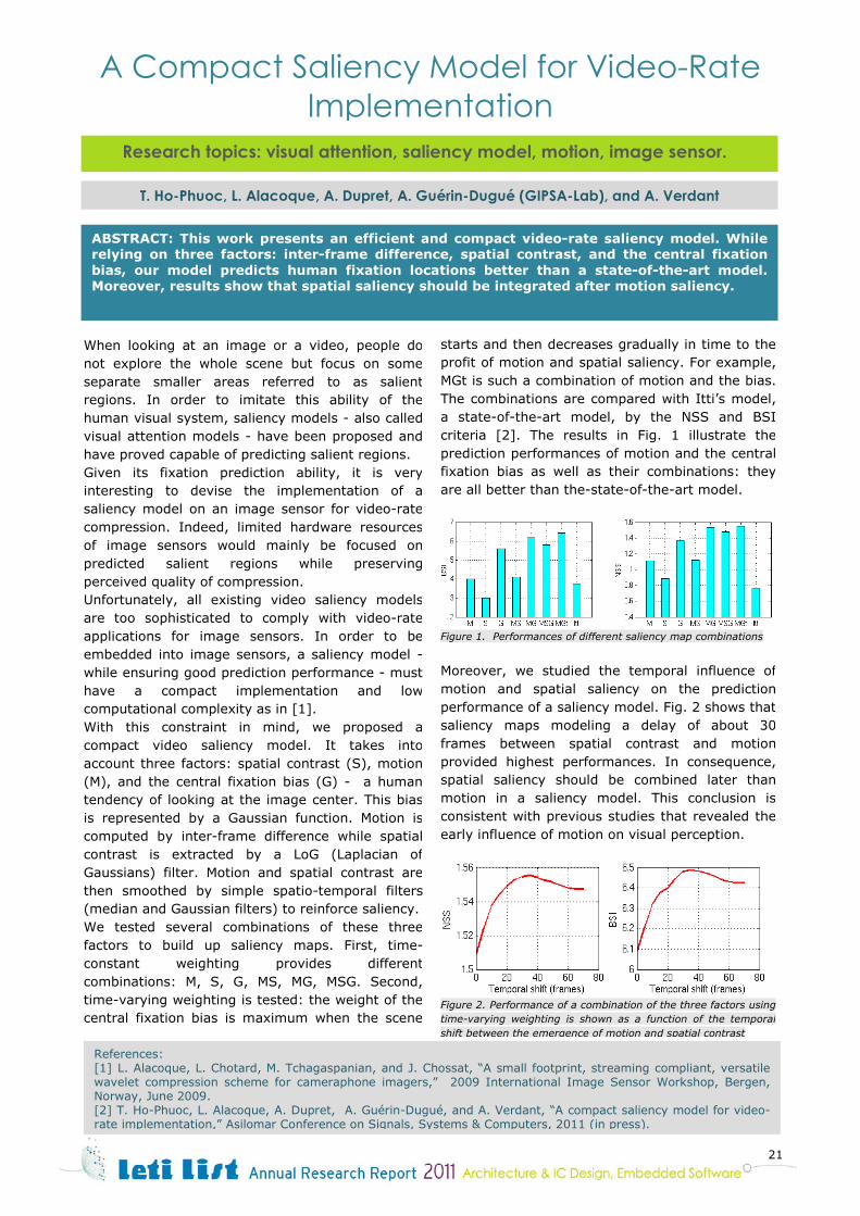
When looking at an image or a video, people do not explore the whole scene but focus on some separate smaller areas referred to as salient regions. In order to imitate this ability of the human visual system, saliency models - also called visual attention models - have been proposed and have proved capable of predicting salient regions. Given its fixation prediction ability, it is very interesting to devise the implementation of a saliency model on an image sensor for video-rate compression. Indeed, limited hardware resources of image sensors would mainly be focused on predicted salient regions while preserving perceived quality of compression. Unfortunately, all existing video saliency models are too sophisticated to comply with video-rate applications for image sensors. In order to be embedded into image sensors, a saliency model - while ensuring good prediction performance - must have a compact implementation and low computational complexity as in [1]. With this constraint in mind, we proposed a compact video saliency model. It takes into account three factors: spatial contrast (S), motion (M), and the central fixation bias (G) - a human tendency of looking at the image center. This bias is represented by a Gaussian function. Motion is computed by inter-frame difference while spatial contrast is extracted by a LoG (Laplacian of Gaussians) filter. Motion and spatial contrast are then smoothed by simple spatio-temporal filters (median and Gaussian filters) to reinforce saliency. We tested several combinations of these three factors to build up saliency maps. First, time-constant weighting provides different combinations: M, S, G, MS, MG, MSG. Second, time-varying weighting is tested: the weight of the central fixation bias is maximum when the scene
starts and then decreases gradually in time to the profit of motion and spatial saliency. For example, MGt is such a combination of motion and the bias. The combinations are compared with Itti’s model, a state-of-the-art model, by the NSS and BSI criteria [2]. The results in Fig. 1 illustrate the prediction performances of motion and the central fixation bias as well as their combinations: they are all better than the-state-of-the-art model.
Figure 1. Performances of different saliency map combinations
Moreover, we studied the temporal influence of motion and spatial saliency on the prediction performance of a saliency model. Fig. 2 shows that saliency maps modeling a delay of about 30 frames between spatial contrast and motion provided highest performances. In consequence, spatial saliency should be combined later than motion in a saliency model. This conclusion is consistent with previous studies that revealed the early influence of motion on visual perception.
Figure 2. Performance of a combination of the three factors using time-varying weighting is shown as a function of the temporal shift between the emergence of motion and spatial contrast
References: [1] L. Alacoque, L. Chotard, M. Tchagaspanian, and J. Chossat, “A small footprint, streaming compliant, versatile wavelet compression scheme for cameraphone imagers,” 2009 International Image Sensor Workshop, Bergen, Norway, June 2009. [2] T. Ho-Phuoc, L. Alacoque, A. Dupret, A. Guérin-Dugué, and A. Verdant, “A compact saliency model for video-rate implementation,” Asilomar Conference on Signals, Systems & Computers, 2011 (in press).

22

23
Architecture, IC Design & Control for Digital SoCs
Adaptive Control & Power Management
3D circuits & NoCs
Multi-Core Architecture
3

24
Control Law Design for Distributed Multi-Agent Systems Applied to Active Clock
Research Topics: PLL network synchronization, Distributed control
A. Korniienko, E. Colinet, G. Scorletti (Ampère Lab.)
ABSTRACT: The problem of PLL network design is reformulated, from a control theory point of view, as a decentralized control law design for a distributed multi-agent system. Inspired by the dissipativity input-output approach, the problem is solved by applying a convex optimization involving simple Linear Matrix Inequality (LMI) constraints.
This usual engineering problem can be generalized as a design problem of a system which is stable and has some desired properties i.e. performance. This problem becomes extremely difficult to solve in the context of networked coupled systems, which is the case for active PLL clock distribution networks [1]. Indeed, we want to design each PLL so as to ensure not only its local stability but also that the overall global system is stable and has some fixed global properties such as synchronization, response time and perturbation rejection. Methods for designing a stand-alone PLL are well-known in the field of microelectronics. However, because of mutual coupling and multiple feedbacks existing in the clock network, there is no guarantee for the global network that it converges to the ”synchronous state” even though each PLL is identical and properly designed to ensure the local convergence on an average input signal. There is also no guarantee that the performance will not be degraded by the network versus the uncoupled separated PLL case. These aspects of global network interconnection and nodes coupling are very important and must be taken into account during the system design procedure. Actually they are beyond the scope of standard one single PLL design methods of microelectronic. Due to the complex dynamic subsystem interactions the design problem becomes a complex control system theory problem. From the decentralized H ∞ control, dissipative input-output approaches and Graph theory, we propose a design procedure which takes into account the network interconnection aspects. This design procedure or algorithm, based on the convex LMI optimization tools, is able to provide a local control law for each subsystem i.e. local PLL filter coefficients that achieve local and global
stability the of overall system as well as some fixed global performance level (see [2] for more details). The algorithm here described was applied to a 4x4 Cartesian two dimensional All-Digital PLL (ADPLL) network where the PLL at the upper-left corner (Fig ?) has one additional external reference input as illustrated. The distribution network generates the clock at 0.97 GHz with frequency divider factor 4. The total number of nodes (PLLs) is 16. As a result, the design algorithm gives a local digital PI filer that ensures local and global stability as well as performance level summarized in Table I. The simulation results are presented in Figure 1.
Time, sec
PLL
freq
uenc
y, H
zEr
ror s
igna
ls, e
.u.
Figure 1. Simulation results of the 4x4 ADPLL network, upper figure represents evolution of node frequencies, and bottom figure is its relative phase error signal evolution
Table I. Ensured performance specification level
Performance objective
Attained level
Synchronization Perfect steady-state reference tracking
Response time At most 3 μsec
Perturbation rejection
Good noise and temperature influence rejection
References: [1] M. Javidan, E. Zianbetov, A. Korniienko, E. Colinet, G. Scorletti, J.–M. Akré, J. Juillard, “All-digital PLL array provides reliable distributed clock for SOCs”, IEEE Conf. ISCAS, Rio de Janeiro, Brazil, mai 2011, pp. 2589–2592. [2] A. Korniienko, G. Scorletti, E. Colinet, E. Blanco, J. Juillard, D. Galayko, “Control Law Synthesis for Distributed Multi-Agent Systems : Application to Active Clock Distribution Network”, IEEE American Control Conference, San Francisco, USA, 2011, pp. 4691–4696.

25
An Innovative Local Adaptive Voltage Scaling Architecture for On-chip Variability
Research topics: MPSoC, energy efficiency, Variability, AVFS, Vdd-hopping
E.Beigné, I. Miro-Panades, Y. Thonnart, P. Vivet ABSTRACT: A fine-grain Adaptive Voltage and Frequency Scaling (LAVFS) architecture is proposed to optimize energy efficiency in presence of in-die variability. For each System-on-Chip power domain, we use a Dynamic Voltage Scaling technique called ‘Vdd-Hopping' as efficient as DC/DC power converters but much easier to integrate and control at fine-grain.
A Local Adaptive Voltage and Frequency Scaling (LAVFS) architecture is proposed by adding adaptive capabilities to a previously proposed Local Dynamic Voltage Scaling (LDVS) scheme [1]. The main objective is to maximize the energy efficiency while complying with performance constraints. The usual AVS paradigm (frequency fixed by the application, supply voltage adjusted by a closed-loop control) is reversed. In our proposal, supply voltages are fixed, while two frequencies and the dithering ratio are dynamically adjusted using an adaptive techniques.
Figure 1. DVS compared to Vdd-hopping with dithering
To avoid using costly and low efficiency DC-DC converters, an efficient and easily integrated method called Vdd-Hopping with dithering [1] is used. At least two voltages are necessary to control the local voltage of a functional core. Figure 1 illustrates the difference between a traditional DVS and the Vdd-Hopping approach. Vdd-Hopping controls the core average frequency Favg by using a dithering ratio between two (or more) power modes and thus reduces the power consumption nearly as efficiently as a continuous voltage converter. In Local Dynamic Voltage Scaling architectures, functional cores are integrated into a wrapper for communication, power supply and power management (Fig 2).
Figure 2. Local DVFS architecture
In such architectures, the clock frequencies associated to the two (or more) selectable power supplies are usually determined at design time using a worst case approach. Our goal is to improve power efficiency by using adaptive techniques at a ‘functional core’ granularity to avoid worst case assumptions and design margins.
Figure 3. Local Adaptive Voltage Scaling architecture proposal
In our innovative system, the voltages are fixed and Fhigh and Flow frequencies are dynamically adjusted according to in-die variability. As those frequencies are changed dynamically, the dithering ratio spent in the ‘high’ and the ‘low’ mode is adjusted accordingly to reach the applicative target average frequency Ftarget. This architecture, based on a GALS approach, is called Local AVFS (Fig. 3) because the frequencies are adjusted independently in every voltage/frequency domain according to local variability factors given by internal HW diagnostic. The performance targets are set by the Global Power Manager providing the most power efficient set of local constraints to optimize the circuit. This architecture allows high gains in terms of energy (from 20% to 60%) and frequency (30%) compared to classic worst-case or DVFS approaches. Using two or three fixed voltage supplies, the circuit is able to dynamically reach an optimal frequency/energy point depending on intrinsic PVT variations and applicative constraints for a low area overhead (~5%).
References: [1] E. Beigné, et al., “An Asynchronous Power Aware and Adaptive NoC based Circuit”, IEEE Journal Of Solid State Circuits, April 2009, vol.44, pp.1167-1177. [3] E. Beigné E., P. Vivet, “An innovative local adaptive voltage scaling architecture for on-chip variability compensation” New Circuits and Systems Conference (NEWCAS), 2011 IEEE 9th International, pp. 510-513

26
Local Condition Monitoring in ICs from a Set of General Purpose Sensors
Research topics: System-on-Chip, power control, variability
L. Vincent, E. Beigné, L. Alacoque, S. Lesecq, C. Bour
ABSTRACT: General purpose sensors such as Ring Oscillators can be used to monitor Voltage (V) and Temperature (T) variations and Process (P) variability. A PVT probe, made of several different Ring Oscillators has been designed to monitor the local condition of a digital circuit. Due to its small size, several PVT probes can be buried within the chip with a very small area overhead, which makes possible the chip monitoring at small scale. The sensors readings must be fused in order to estimate the PVT state. In order to ensure adaptivity capabilities of today computing platforms, sensors must be buried within the chip to monitor the Temperature (T), Voltage (V) and Process (P) variations. From their readings, alarms can be raised in order to set the system in a safe mode. Moreover, in adaptive architectures, some parameters can be tuned in order to ensure, for the platform, given performances, even under PVT variations. Sensors developed to monitor the PVT state can be split in two families. The first one contains ”specialized” sensors designed to be sensitive to only one of the variability factors. Unfortunately, their design is tricky as they must be insensitive to all but one parameter. Moreover, they are mainly analog. The second family contains general purpose sensors, built from standard digital blocks, that are sensitive to several parameters. For example, the frequency F at a Ring Oscillator (RO) output depends on its current PVT state, see Figure 1.
Figure 1: F=f(V,T), at typical process, for the temperature dedicated probe (after RC extraction).
The objective of this study was to design the so-called MultiProbe IP, based on 7 different ROs. All the constituting ROs are sensitive to PVT variations but in a slightly different way. For modularity purpose, all the distributed MultiProbes are chained so that a unique controller needs to be implemented on the circuit. Due to its low area, the MultiProbe can be buried in the Silicon area that has to be monitored. Figure 2 provides a block diagram of the MultiProbe.
Figure 2: block diagram of the MultiProbe. Note that a particular temperature dependent RO based on current-starved inverters biased by a thermally dependent current generator is embedded in the MultiProbe. The output of such sensors cannot directly provide information on the PVT state. Thus, future work will develop data fusion techniques in order to extract from the MultiProbe readings the PVT state of the Silicon area where the sensor is buried.
References: [1] L. Vincent, E. Beigne, L. Alacoque, S. Lesecq, C. Bour, Ph. Maurine, “A New Architecture of a Low Area Integrated Sensor to Measure Process, Temperature and Voltage Variations Along Digital SoCs”, VARI 2011, Grenoble, France.

27
Robust Control of a DFLL for Power Management in MPSoC
Research topics: Control Theory, Variability, System-on-Chip
Y. Akgul, C. Albea-Sanchez, S. Lesecq, D. Puschini
ABSTRACT: The control at fine grain of supply voltage and clock frequency in a GALS architecture requires to develop robust and simple control engine in order to ensure that, even under parameter uncertainties, temperature variations and process variability, the closed-loop system still performs properly. We have developed the control engine of a Digital Frequency Locked Loop using several approaches from the control community.
Fine-grain Dynamic Voltage and Frequency Scaling (DVFS) is becoming a requirement for Globally-Asynchronous Locally-Synchronous (GALS) architectures to ensure low power consumption of the whole chip. Each voltage/frequency island is driven by a voltage “actuator” and a frequency “actuator”. However, due to process variability that naturally appears with technology scaling, the actuator and control law design must be robust [1] and the latter must be as simple as possible [5]. Moreover, the area overhead of adding voltage and frequency control engines to each voltage/frequency island must be taken into account to optimize the circuit. Last but not least, the response time constraints require these controllers to be implemented in hardware [3].
The main objective of this study is to design the control engine of a Digital Frequency Locked Loop (DFLL), see Figure 1. The closed-loop system must fulfill stringent requirements in terms of response time, overshoot, and robustness against parameters uncertainties.
Figure 1: DFLL block diagram
The system has been first modeled with behavioral
models. Especially, the delay that naturally arises in the sensor block has been taken into account.
Several control techniques have been applied to deal with the design of the control engine for the frequency “actuator”. Actually, each one of these techniques allows taking into account particular characteristics of the system. For instance, [4][2] are based upon non-linear control approaches. They naturally take into account saturations that exist at the output of the controller block depicted in Figure 2, via the use of Lyapunov-Krasovskii theory that ensures asymptotic stability, disturbance rejection as well as system robustness with respect to delay presence and parameter uncertainties. [5] makes use of linear control theory while taking account of the parameter uncertainties. The control law is a simple integrator and its parameter tuning is very intuitive, increasing the re-use of this block for other DFLL configurations.
Figure 2: block diagram for the DFLL
The control engine has been implemented in hardware with ad-hoc fixed-point arithmetic [3] format.
References: [1] S. Lesecq, D. Puschini, E. Beigné, P. Vivet, Y. Akgul, “Low-Cost and Robust Control of a DFLL for Multi-Processor System-on-Chip”, IFAC World congress, Milano, Italy, August 28 – September 2, 2011. [2] C. Albea-Sanchez, S. Lesecq, D. Puschini, “Optimal and Robust Saturated Control for a Clock Generator”, 50th IEEE Conference on Decision and Control and European Control Conference CDC-ECC’11, Orlando, USA, Dec. 2011. [3] C. Albea-Sanchez, D. Puschini, P. Vivet, I. Miro-Panades, E. Beigné, S. Lesecq, "Architecture and Robust Control of a Digital Frequency-Locked Loop for Fine-Grain Dynamic Voltage and Frequency Scaling in Globally Asynchronous Locally Synchronous Structures", Journal of Low Power Electronics, Vol. 7, 1–13, 2011. [4] C. Albea-Sanchez, D. Puschini, S. Lesecq, E. Beigné, “Optimal and robust control for a small-area FLL”, 19th Mediterranean Conference on Control and Automation MED’11, Corfu, Greece, June 20-23 2011. [5] S. Lesecq, D. Puschini, E. Beigné, P. Vivet, “Robust pole placement techniques applied to the control design for a DFLL under PVT-variability”, 2nd European Workshop on CMOS Variability, Grenoble, France, May 30-31, 2011.

28
Reducing Power Consumption in Turbo Decoders
Research topics: architecture, turbo-decoders, power-consumption
P. Reddy, F. Clermidy, A. Baghdadi (Telecom Bretagne) ABSTRACT: Turbo-decoders consume up to 50% of a Telecom baseband featuring high throughputs like 3GPP-LTE. These very computing-intensive units are working on an iteration base in order to recover corrupted data. In this work, we show how applying new stopping criteria to iterations can save 23% more power consumption compared to existing techniques.
Turbo-decoding is an attractive channel decoding scheme and is widely used in wireless communication. The superior performance of turbo codes comes from the combination of parallel concatenated coding, recursive encoding, pseudorandom interleaving and iterative decoding. However, this performance comes at the cost of an important computational complexity. In the mobile terminals, this complexity is directly related to power consumption. As an example, the decoder of a 3GPP-LTE application in [2] is responsible for 60% of the total baseband power consumption at 50 Mbits/s throughput. Thus, turbo-decoders have to balance the two conflicting requirements of low-energy consumption and high-performance requirements. A typical turbo-decoder includes two Soft-Input/Soft-Output (SISO) decoders as well as interleaver and de-interleaver units between the decoders and a simple comparator for deducing the hard decision (0 or 1).
DEC1Π
Π-1
DEC2
Π
Fig. 1. Typical Turbo-decoder architecture
As turbo decoding is an iterative process, a special criterion, called stopping criterion can be used to determine the convergence of the decoding, and finally the iteration i where the decoding process can be terminated. However, methods used in state-of-the-art always come with some hardware overhead.
In our work, a new stopping criterion based on internal trellis states is proposed. The advantage of trellis is the low hardware overhead thanks to the use of states coded on few bits as key parameter to stop the iterative process.
LLRC LLRTC TB LCTB
Power (mW)
Memory + Address Generator + Buffer 7.02 - 2.34 -
Registers + Comparator + Counter
0.04 0.04 0.02 0.02
Total Power Overhead (per iteration)
7.06 0.04 2.36 0.02
Area (mm²)
Memory + Address Generator + Buffer 0.0676 - 0.0309 -
Registers + Comparator + Counter
0.0037 0.0037 0.0037 0.0037
Total Area Overhead 0.0713 0.0037 0.0346 0.0037 Fig. 2. Power consumption and area overhead of added hardware for TB techniques compared to LLR-based SOTA techniques
Two versions have been proposed, a basic Trellis Based (TB) technique and a Low-Complexity (LCTB) version further saving real estate. These new stopping criteria have been compared to state-of-the-art techniques and are showing good improvement of 23% power consumption for a comparable Bit Error Rate (BER).
0
50
100
150
200
250
300
350
0 0,1 0,2 0,3 0,4 0,5 0,6 0,7 0,8 0,9 1 1,1 1,2
SNR (db)
Pow
er C
onsu
mpt
ion
(mW
)
FixedMGLLRCLLRTCTBLCTB
0
50
100
150
200
250
300
350
0 0,1 0,2 0,3 0,4 0,5 0,6 0,7 0,8 0,9 1 1,1 1,2
SNR (db)
Pow
er C
onsu
mpt
ion
(mW
)
FixedMGLLRCLLRTCTBLCTB
Fig. 3. Power consumption for different SNR
References: [1] P. Reddy, F. Clermidy, A. Baghdadi, M. Jezequel, “A New Trellis Based Stopping Criteria for Reducing Power Consumption in Turbo Decoders”, Conference on Design Automation and Test in Europe, DATE’11, March 2011 [2] F.Clermidy, C. Bernard, R. Lemaire, J. Martin, I. Miro-Panades, Y. Thonnart, P. Vivet, N. Wehn “A 477mW NoC-Based Digital Baseband for MIMO 4G SDR”, International Symposium on Solid State Circuits, ISSCC’10, San-Francisco, USA, Feb. 2010

29
A multi-source power management module for autonomous sensor nodes
Research topics: Autonomous harvesting microsystem, Asynchronous control
J.F. Christmann, E. Beigné, C. Condemine, J. Willemin, C. Piguet (CSEM)
ABSTRACT: This work focuses on the design of a power management module targeting autonomous wireless sensor node applications. Based on a multiple power paths architecture configured with a dedicated asynchronous controller, the module is implemented in UMC 180nm CMOS process.
In the field of wireless sensor nodes, two key success factors are relevant to reach energy autonomy. On one hand, high global power efficiency is mandatory from the sources to the sensors. On the other hand, the circuit has to implement ultra low energy monitoring and conversion. The aim of this work is to develop a wireless sensing microsystem involving multi-energy harvesting (solar, thermal, electro-magnetic and vibratory energy sources) and an innovative energy management policy which relies on several supply power paths and asynchronous control [1]. Fig. 1 illustrates the classical power paths which can massively be found in the literature .This work proposes al direct power path providing high power efficiency.
DIGITALCONTROLLERPower management
External LoadsC.O.T.S. Components
Energy harvesters
TEG
PV cell
Internal LoadsADC SAR and ΣΔ
MA
NA
GY++
+++
+++
++
-
+-
DIR
ECT
PATH
Microbattery
Vib
RFDIGITAL
CONTROLLERPower management
External LoadsC.O.T.S. ComponentsExternal LoadsC.O.T.S. Components
Energy harvesters
TEG
PV cell
Internal LoadsADC SAR and ΣΔ
Internal LoadsADC SAR and ΣΔ
MA
NA
GY++++
+++ +++
+++
++
- +++
++
-
+-+-
DIR
ECT
PATH
MicrobatteryMicrobattery
Vib
RF
Fig. 1 Multiple power paths principle overview
The classical indirect power path uses the harvested energy to charge a battery. Once energy is needed, the battery is discharged to supply the requesting power load. On the contrary, the direct power path is used when, at the same time, energy is harvested and power supply is requested, providing high power efficiency. As the direct power path depends on the harvested energy level, the indirect power path can also be used at the cost of a lower power efficiency.
Use of these multiple power paths is managed by a dedicated controller which reconfigures the power path according to harvested energy levels and battery state of charge. By dynamically reconfiguring the power paths, the system is thus able to ensure optimal power efficiency. Leveraging asynchronous QDI (Quasi Delay Insensitive) logic benefits such as supply voltage levels and variations robustness, automatic idle mode and smooth current profile, the dedicated controller is event-driven. By converting energy events such as voltage threshold crossing into data events, the controller is informed about energy levels within the microsystem. It can thus perform adaptive energy-driven reconfiguration of the architecture. The whole power management module is implemented in 180nm CMOS process because of its low leakage features. Fig. 2 illustrates the layout of the module, whose area is 0.96mm².
Fig.2 Layout of the power management module Involving a synchronous version of the controller, comparisons between the two controllers will be done in order to validate the choice of asynchronous logic. Moreover, thanks to various typical wireless sensing applications scenarios, this work aims to determine the effective gain of the multi power paths architecture, according to energy availability, compared to the classical indirect power path architecture, charging and discharging the battery.
References: [1] J.-F. Christmann, E. Beigne, C. Condemine, P. Vivet, J. Willemin, N. Leblond, and C. Piguet, « Bringing Robustness and Power Efficiency to Autonomous Energy-Harvesting Microsystems », IEEE Design & Test of Computers, vol. 28, no. 5, p. 84-94, oct. 2011.

30
Power Gating in 65nm PD-SOI Technology
Research topics: SOI, Power Gating, Leakage Current
J. Le Coz (ST), P. Flatresse (ST), A. Valentian, M. Belleville ABSTRACT: This work was carried out on Power Gating in Partially-Depleted SOI technology, in order to reduce one major drawback of this technology, i.e. its leakage current. We have shown that, thanks to SOI-optimized (1) Power Switch structure and (2) retention Flip-Flops, leakage can be lower than in Bulk CMOS when power is gated.
Partially-Depleted SOI technology has a number of advantages over Bulk CMOS technology, namely speed and dynamic power dissipation, due to its lower parasitic capacitances and dynamic threshold voltage (VT) modulation. However, this VT modulation also leads to much higher leakage currents than in Bulk, hampering the adoption of this technology in portable applications. Since it is not possible to tie the body of each SOI transistor for controling its VT value in sleep mode, the only way to cut leakage currents is to gate the power supply by introducing so-called Power Switches, a trend increasingly found in Bulk also. A special kind of Power Switch was developed in order to take benefit from the advantages of SOI technology. This Power Switch is based on a High-VT transistor, for having the lowest leakage currents when OFF, to which we added a Forward-Body-Biasing circuit, described in Fig. 1.
Fig. 1 Auto-adaptive forward-body-biased power switching.
This Forward-Body Biasing circuit is activated only when the Power Switches are ON, in order to reduce their electrical resistance and the associated voltage drop. We call this specific solution “Auto-DTMOS” because it automatically produces a Dynamic Threshold MOS (DTMOS) effect. These Auto-DTMOS Power Switches were
implemented on silicon in PD-SOI 65 nm technology. Their implementation consisted of a ring of 3500 abutted power switches, controlled by four body-biasing circuits (i.e. one for every 1,000 power switches). For comparison purposes, rings of Floating Body (FB) and Body Contacted (BC) Power Switches were also implemented. Results indicate a 20% improvement of the ON resistance of the Auto-DTMOS solution. The previous results were obtained from a standalone testchip. This Power Switch was also implemented in a Low Density Parity Check (LDPC) testchip. Compared to the Bulk implementation, it shows a 20% reduction of leakage current at same Vdd, reaching 50% when considering the same operating frequency (obtained with a lower supply voltage value).
Table 1 Comparison of Bulk and PD-SOI leakage currents.
In addition, during OFF mode, Retention Flip-Flops are required to store the logical state of a circuit, in order to restore it when power is switched ON again. In this work a Retention Flip-Flop, optimized for robust functionality and Low-Stand-by Power features in PD-SOI technology, has also been proposed. The use of body contacted or stacked floating body devices, in the retention memory, has been explored, and the best tradeoff is based on the stacked devices, leading to the best retention leakage gain (50 to 70% reduction), for a small area overhead (6%) and no speed penalty, when compared to a similar floating body implementation. Those results pave the way toward PD-SOI circuits exhibiting a lower operating power for an equivalent stand-by power, than equivalent CMOS bulk circuits
References: [1] Julien Le Coz et al., “Comparison of 65nm LP Bulk and LP PD-SOI with Adaptive Power Gate Body Bias for an LDPC Codec,” ISSCC, San Francisco, USA, Feb. 2011 [2] Julien Le Coz et al., “65nm PD-SOI Glitch-Free Retention Flip-Flop for MTCMOS Power Switch applications,” ICICDT, Kaoshiung, Taiwan, 2011

31
A Low Jitter 65nm PD-SOI Output Buffer
Research topics: Output Buffer, Jitter, PD-SOI, History effect
D. Soussan (ST), S. Majcherczak (ST), A. Valentian, M. Belleville
ABSTRACT: In this work, a new active body-biasing control technique is proposed and used in a PD-SOI output buffer of an I/O library. It allows to overcome the additional jitter related to PD-SOI history effect, as well as the higher static leakage current compared to bulk technology.
An output circuit is made of two paths: the upper one is dedicated to the output buffer pMOS drive whereas the lower one is dedicated to the nMOS drive (Fig. 1.). Each path includes a level shifter and a slew rate control of the N & P output buffers.
In
Pre Driver Output Buffer
ND
PDOUTP
OUTN
Vdd Vdde
Gnd Gnde
Out
Level-Up Shifter
CLOAD
Vdd Vdde
Gnd Gnde
Vdde
Gnde
Vdde
Gnde
Vdd=1.2v Vdde=2.5v
Vdde
Gnde
NBuffer
PBuffer
BODY CONTACTED (to Supply Voltage) SCOPE OF THIS WORK
In
Pre Driver Output Buffer
ND
PDOUTP
OUTN
Vdd Vdde
Gnd Gnde
Out
Level-Up Shifter
CLOAD
Vdd Vdde
Gnd Gnde
Vdde
Gnde
Vdde
Gnde
Vdd=1.2v Vdde=2.5v
Vdde
Gnde
NBuffer
PBuffer
BODY CONTACTED (to Supply Voltage) SCOPE OF THIS WORK
Fig. 1. Output buffer circuit principle Within I/O design, output jitter is one of the main parameters to be considered in order to keep high signal integrity. This work is focused on the Data Dependent (DD) jitter which reflects the timing variation induced by data-type signal. For large capacitive loads and during a short-bit sequence, there is not enough time (due to a lack of drive current) for the output signal to fully reach the supply voltages before the next transition. This leads to timing uncertainty, compared to long-bit sequences. Partially Depleted Silicon-on-Insulator (PD-SOI) technology is attractive for its performance improvement (in core digital and I/O circuits) and also for its latch-up immunity. However, due to its floating body effect, timings can be affected by the so-called « History effect ». In this work case, this leads to about 20ps of additional DD jitter. In addition, the self-body biasing of the floating-body transistors also induces higher static current.
gnde
Out
ND
Nbody gnde
Switching TimeOFF ON
VT VT VT
FBB
gnde
Out
ND
Nbody gnde
Switching TimeOFF ON
VT VT VT
FBBND
Nbody
Out
Gnde
Gnde
Nbuffer
N1
I1 N2
ABC Circuit
B
S
D
G
ND
Nbody
Out
Gnde
Gnde
Nbuffer
N1
I1 N2
ABC Circuit
B
S
D
G
Fig. 2. Active Body-biasing Control (ABC) circuit
The aim of the proposed circuit (Fig. 2.) is to overcome those two problems. To this end, VT of the output buffer is controlled, and dynamically modulated through body biasing so as to improve transition time by lowering VT during switching time, and to reduce static current by increasing VT during steady state.
Fig. 3. Output signal Jitter vs Output Capacitive load
Compared to Floating Body (FB) and Body Contacted to Source (BC) alternatives (Fig. 3.) this circuit suppresses the History effect impact, and exhibits the best results whatever the capacitive load and the temperature.
References: [1] D.Soussan, S. Majcherczak, A. Valentian, M. Belleville, “A Low Jitter Active Body-Biasing Control-based Output Buffer in 65nm PD-SOI”, IEEE International Conference on IC Design & Technology (ICICDT), 2011, Kaoshiung.

32
3D NoC using Through Silicon Via: An Asynchronous Implementation
Research topics: 3D Integration, Network-on-Chip, Asynchronous Design
P. Vivet, F. Darve, Y. Thonnart, D. Dutoit, F. Clermidy ABSTRACT: To offer robust and high bandwidth communication in a 3D stack, a 3D asynchronous NoC has been designed in a CMOS 65nm technology. By using asynchronous serial link to further reduce the TSV count while preserving throughput, the 3D ANOC delivers an aggregate bandwidth of 16 GB/s for a reduced power consumption compared to LPDDR2.
3D stacking is seen as one of the most promising technologies for future System-on-Chip (SoC) developments. However, 3D technologies using Through Silicon Vias (TSV) have not yet proved their viability for deployment in large-range of products. In this paper, we are investigating 3D Network-on-Chip as a promising solution for increased modularity and scalability. The proposed 3D-ANoC communication infra-structure [2,3] is fully implemented in the so-called Quasi-Delay Insensitive asynchronous logic, a very robust class of unclocked logic which brings robustness to Process, Voltage and Temperature. This Globally Asynchronous Locally Synchronous 3D architecture allows to get rid of any global timing and clocking constraints, both in the 2D direction (within die sub-units) as well as in the 3D direction (through the TSVs).
2D NoC Router
3D NoC Router
Processing Unit
NoC Serial Links
Figure 1. 3D-ANoC Architecture overview
In order to further reduce the impact of TSVs on 3D connections, the 3D-ANoC (Fig 1) integrates asynchronous serial links. The serialization is fully implemented with asynchronous logic, using 4 phase protocol and 1-of-4 encoding. The serialization ratio is then a trade-off between TSV count and 3D communication throughput. In this work, we have selected a serialization factor of 4.
For testability and yield purposes, the 3D-ANoC architecture also integrates some 3D DFT infrastructure based on boundary scan using IEEE 1149.1 JTAG; as well as a TSV fault tolerance scheme using spare and repair TSVs. The 3D-ANOC router has been fully implemented, using a TSV middle Vt CMOS 65nm STMicroelectronics technology (fig 2).
Figure 2. 3D Router floorplan
Compared to existing LPDDR2 protocol, our 3D-ANOC serial link achieves 500MHz frequency, for an aggregate bandwidth of 16 GB/s, a reduced power consumption, while using only 178 TSVs.
Table 1: LPDDR2/ANOC performance comparison [1][3].
#IO
#bits & frequency
Throughput
Interface Power
Consumption LPDDR2 208 Pads
2 * 32 bits
@ 533 MHZ 4.264 GB/s 680 mW
ANoC (x4 serial link)
178 TSVs 2 * 128 bits @ 500MHz
16 GB/s 425 mW
Using robust communication, the 3D-ANoC architecture remains functional in case of any source of 3D variability: heterogeneous stack, in-die variability, TSV delay, power or thermal degradation. For future multi-cores, 3D-ANoC also brings an efficient packet based communication infrastructure to connect multiple dies together.
References: [1] Fabien Clermidy, Florian Darve, Denis Dutoit, Walid Lafi, Pascal Vivet, “3D Embedded multi-core: Some perspectives”, DATE 2011, Grenoble, France, March 2011, pp. 1327-1332 [2] Florian Darve, Abbas Sheibanyrad, Pascal Vivet, Frédéric Pétrot, “Physical Implementation of an Asynchronous 3D-NoC Router Using Serial Vertical Links”. ISVLSI 2011, Chennai, India, July 2011, pp. 25-30 [3] Pascal Vivet, Denis Dutoit, Yvain Thonnart, Fabien Clermidy, “3D NoC using through silicon Via: An asynchronous implementation”, VLSI-SoC 2011, Hong Kong, China, Oct 2011, pp. 232-237

33
A Stackable LTE Chip for Cost-effective 3D Systems
Research topics: 3D integration, cost analysis, LTE telecom applications.
W. Lafi, D. Lattard, A. Jerraya
ABSTRACT: To address the problem the of prohibitive cost of advanced manufacturing technologies, one solution consists in reusing masks to address a wide range of ICs. In the case of 4G wireless telecom applications, this could be achieved by a modular circuit that can be stacked to build TSV-based 3D systems with data rate adapted to market segments. In this work, we compare several 3D integration approaches to a 2D reference chip.
In the case of mobile phones, the 4G standard provides several transmission modes depending on the desired throughput and robustness. We propose a reconfigurable NoC-based circuit for 4G telecom applications. When used alone, the proposed circuit can meet the requirements of the Single Input Single Output (SISO) mode of transmission. By stacking multiple instances of this basic circuit, using vertical links of the 3D NoC and performing some software reconfigurations, it will be possible to boost system performance and address several Multiple Input Multiple Output (MIMO) modes [1]. Consequently, it would be possible to meet the requirements of each transmission mode with the same mask set. Coupled to heterogeneous integration, this same die stacking approach, is an efficient way to build modular 3D SoC (as shown in Fig. 1).
Figure 1. Example of a 3D system We have developed a system-level cost analysis tool that allows having a preliminary cost estimation of a 3D system, and deciding on the best options to choose in order to optimize cost [2]. This exploration tool has been used to compare the cost of a 2D reference chip to its 3D versions. We focus on 3 stacking approaches: the Wafer-to-Wafer (W2W), the Die-to-Wafer (D2W)
and the Interposer-based Stacking (IbS). The IbS approach is to stack several dies (fabricated in an aggressive technology such as 28 nm) on top of a silicon interposer fabricated using a mature technology such as 130 nm in order to improve fabrication yield. The cost model takes technology yield, stacking operations, fabrication and test costs into account. Figure 2 shows the variation of unit cost according to die area, in the case of 3D systems based on the same die approach.
Interposer
2D
3D W2W
3D D2W
3D IbS
0
100
200
300
400
500
600
700
800
0 50 100 150 200 250 300
Uni
t cos
t(€)
2D circuit area (mm2)
Production volume = 1 million
2D
3D W2W
3D D2W
3D IbS
2 layers28 nm technology
Figure 2. Cost vs chip area In the case of large-sized design, the D2W and IbS 3D stacking become the most cost-effective approaches. As an illustration, the D2W stacking allows reducing cost (compared to the 2D approach) by 20% when the design area is 250mm2. Due to the statistical location of bad dies, the W2W scheme leads to extremely low yields and is thus economically not viable. We can conclude that 3D stacking involves extra-fees due to additional steps of the 3D fabrication process (such as bonding, TSV formation, known-good-die test...), but also allows cost reduction by reducing the area of the stacked dies and then improving yield. Therefore, the IbS approach is the most cost effective 3D integration scheme in the case of large-sized circuits.
Reference: [1] W. Lafi, D. Lattard and A. Jerraya, “An Asynchronous Hierarchical Router for NoC-based 3D MPSoCs”, Journal of Software, Practice and Experience, Special Issue, published by John Wiley & Sons Ltd, 2012. [2] W. Lafi, D. Lattard and A. Jerraya, “A stackable LTE chip for cost-effective 3D systems”, IPSJ Transactions on System LSI Design Methodology, Invited Paper, Vol.5, February 2012.

34
Dynamic Flow Reconfiguration Strategy to Avoid Communication Hot-Spots
Research topics: dynamic routing, hot spots, re-ordering
Romain Prolonge, Fabien Clermidy, Leonel Tedesco and Fernando Moraes (PUCRS)
ABSTRACT: In Network-on-Chip architectures, data flows are sent from a source unit to a target (one??) through a network. These flows can interact with each other providing a dynamic flow graph which can be handled with a dynamic reconfiguration strategy. However, it can lead to unordered data deliveries with costly re-ordering units. We propose a coarse grain dynamic reconfiguration which avoids data re-ordering requirement.
The variety of applications, associated to high masks costs, are leading to more flexible, more generic, more programmable SoCs. Similarly, applications are moving to be more data-dependent and despite the fact that flows of data are still predictable, their sizes and their occurrence in time become difficult to compute off-line. This problem can lead to over-sizing the Network-on-Chip (NoC), as it will be designed in a worst case configuration. One way to solve this issue is to propose a dynamic flow management. Such strategy is efficient but leads to two issues which must be solved: (a) assuring that the new routing is deadlock-free; (b) re-ordering the data at the arrival. The first problem has been widely studied in the past. The second issue implies a high complexity mechanism, as well as area overhead. We propose a re-ordering free dynamic flow reconfiguration [1]. Contrary to previous works, we propose a solution where, by construction, the re-ordering is not needed. In other words, the method performs an adaptive source routing mechanism and guarantees the right order in the data deliveries without requiring any re-ordering unit in the target node. In the proposed model, we leverage on two concepts: (a) a flow control by the mean of a credit/data exchange mechanism between the source of data and the corresponding target; (b) the source routing which gives the possibility to change the path at the source node. Our method relies on monitoring congestion levels on each routing paths. When a congestion is detected, the flow carries this information towards the target unit. After its reception, the target unit sends a message to the source unit. This message informs the source of the presence and the location of the congestion. Moreover, the source stops immediately the flow emission. Then, the target resource waits until the amount of credits it sent equals the amount of data it received. So, at the
end, there is no remaining data on the jammed path. This feature guarantees the right order in the data arrival. After that, the target unit triggers a new path computation in the source unit. Then, the flow resumes with the new congestion-free path. The implementation of the method shows that the area overhead corresponds to an equivalent storage area of 4 packets in a Low-Power 65nm technology. When compared to previous re-ordering techniques, our method is less area consuming. Based on this methodology and its corresponding implementation, we have performed some experiments in hot-spots contexts to see the impact of the adaptive routing algorithm on the messages latency. As shown in Fig.1, for a given message length, latency reduction increases until the hot spot length becomes greater than the message one. After this point, the latency reduction levels off. This value represents the greatest latency reduction that can obtain a message of this length. Moreover, this value increases with the message length. As a result, up to 33% of latency can be saved.
Fig.1 – Latency reduction according to message and hot-spot lengths
References: [1] R. Prolonge, F. Clermidy, L. Tedesco, et F. Moraes, “Dynamic Flow Reconfiguration Strategy to Avoid Communication Hot-Spots”, in 2011 14th Euromicro Conference on Digital System Design (DSD), 2011, p. 519-524.

35
AHDAM: an Asymmetric Homogeneous Many-core Architecture
Research topics: multithreaded processor, many-core, dynamic applications
C. Bechara and N. Ventroux / D. Etiemble (LRI)
ABSTRACT: In this work, we designed a many-core architecture named AHDAM. This architecture uses a specific control unit to dynamically balance the workload on different tiles. Each tile is composed of a master processor and a set of secondary VLIW processors to process OpenMP loop nets. The 136 many-core architecture reaches 140Gops on 51.92 mm2 (40nm) i.e. 2.69GOPS/mm².
The future high-end embedded applications are characterized by their computation-intensive workloads, their high-level of parallelism, their large data-set requirements, and their dynamism. Those applications require highly-efficient manycore architectures. In response to this problem, we designed an asymmetric homogeneous manycore architecture called AHDAM. AHDAM exploits the parallelism on all its granularity levels (task, loop and instruction levels). It implements multithreading techniques to increase the processors' utilization [1,3]. We designed an easy programming model and reused the semi-automatic source-to-source parallelization tool Par4All from HPC Project. The AHDAM chip architecture uses a specific control unit to dynamically load balance tasks on different tiles, through a control bus, to master processors (MPE) [2]. A tile is composed of on MPE and a set of secondary processors (LPEs) to process net loops. Each task has serial and parallel regions. The parallel regions are the parallelized loop implemented by using a fork-join programming model such as OpenMP. The MPE executes the serial regions of the tasks. When it encounters a loop region using OpenMP pragmas, the MPE executes a scheduling algorithm that uses a heuristic to fork the exact number of child threads in the appropriate Tiles' Thread Context Pool. The local MPE can fork child threads in others Thread Context Pool by verifying their availability using the shared TCP state memory. The master thread who forks the child threads, waits to join until all the child threads have finished their execution. All tiles share a DDR access to handle data and a local instruction memory through a multibus. MPEs are implemented as monothreaded MIPS32 24K with FPU, while LPEs are implemented as 2-threaded 3-way VLIW processors. The CCP is
the AntX 32-bit 5-stage RISC processor.
To study its performance, we used a radio spectrum sensing application from Thales Communication France. On a simulation framework, we evaluated sequential and parallel versions of the application on two platforms: single processor, and AHDAM with a variable number of processors (up to 136). Our architecture meets the real-time deadline of the application and reaches 140 Gops, while occupying 51.92 mm2 at 40 nm technology. This represents a transistor efficiency of 2.69GOPS/mm², compared to 0.11GOPS/mm² for a MIPS24K.
References: [1] C. Bechara, N. Ventroux and D. Etiemble, “AHDAM: an Asymmetric Homogeneous with Dynamic Allocation Manycore chip, Facing the Multicore-Challenge II”, Springer-Verlag LNCS 6310, Karlsruhe, Germany, Sep. 2011. [2] C. Bechara, N. Ventroux and D. Etiemble, “Comparison of different thread scheduling strategies for Asymmetric Chip MultiThreading architectures in embedded systems”, DSD, Oulu, Finland, Sep. 2011. [3] C. Bechara, N. Ventroux and D. Etiemble, “A TLM-based Multithreaded Instruction Set Simulator for MPSoC Simulation Environment”, RAPIDO, Crete, Greece, January 2011.

36
Interleaved Multithreaded Processor for Embedded Systems
Research topics: multithreaded processor, embedded systems
C. Bechara, A. Berhault, N. Ventroux, S. Chevobbe, Y. Lhuillier, R. David, D. Etiemble (LRI)
ABSTRACT: In this work, we designed a small footprint interleaved multithreaded processor based on the AntX 5 stage RISC processor. This processor can support two virtual threads and uses only 13.97 Kgates. The performance gain is 17% when compared to the monothreaded core for a 73.2% area increase.
With the increase in the design complexity of MPSoC architectures and the need for more transistor/energy efficient processor architectures, designers are exploiting the parallelism at the thread level (TLP) through the implementation of embedded multithreaded processors. Moreover, future manycore architectures tend to use small footprint cores. In this work, we present a small footprint, scalar, in-order, 5-stage pipeline, interleaved multithreaded processor with two hardware thread contexts for embedded systems and SoC integration [1]. Recent small multi-threaded processors for embedded systems have been designed. The figure below shows the main existing works among interleaved multithreaded (IMT) and blocked multithreaded embedded (BMT) processors.
The monothreaded core, on which we have based our study, is called AntX. It has lot of similarities with MIPS-I R3000 but has been designed to ease the specialization of the core with dedicated extensions. AntX is a 5-stage pipeline mono-threaded RISC core. It is a mix 16-32-bit instruction set with 32-bit wide datapath. It is well-suited for low-cost control in MPSoC environment. Therefore, there are no complex units such as a branch predictor, FPUs and multipliers. Its register file is composed of 16 32-bit registers. AntX comes along with a dedicated GNU tool chain. The ISA supports a variable instruction size (16/32 bit) in order to reduce the instruction memory footprint. So, some basic arithmetic/logic/comparison/jump
instructions are coded in 16-bit, while other more complex instructions are coded in 32-bit.
Synthesis results in 40 nm TSMC shows that the multithreaded core area is only 19800 µm2 and 13.97Kgates, which is almost equal to a 4KB direct mapped cache memory according to CACTI 6.5 tool. The IMT core area increase is 73.2% compared to the monothreaded core. The IMT RTL model is validated by executing 2 instances of a simple bubble-sort application concurrently, while varying the L1 D$ size. The extracted pipeline statistics showed that the IMT model is able to hide all the pipeline stalls due to data dependencies between instructions and branch penalties. The IMT core gives an average performance gain of 17% compared to the monothreaded core as shown below.
References: [1] C. Bechara, A. Berhault, N. Ventroux, S. Chevobbe, Y. Lhuillier, R. David and D. Etiemble, “A Small Footprint Interleaved Multithreaded Processor for Embedded Systems”, IEEE International Conference on Electronics, Circuits, and Systems (ICECS), Beirut, Lebanon, December 2011.

37
Dynamic Routing Strategy for Embedded Distributed Architectures
Research topics: Embedded distributed manycores ; Routing
C. Azar, S. Chevobbe, Y. Lhuillier and J.P. Diguet (UBS/LABSTICC) ABSTRACT: Manycore architectures gained a large interest over the years but the problem remains in scaling the control fabric and the interconnection network. In this work we present CEDAR, a Configurable Embedded Distributed ARchitecture, and its adaptive routing strategy based on ACO (Ant Colony Optimization). Routing paths for remote data transfers are defined at runtime and allow a homogeneous distribution of traffic.
The number of cores of parallel architectures is expected to scale rapidly and the issue of the interconnection network is a serious threat that jeopardizes their usability. One of the major problems arises from non scalable global wire delays. To overcome this issue, designers have introduced a communication-centric approach based on Network-On-Chips (NoCs), favoring short communication links. While NoCs constitute a fair solution for nowadays interconnection architectures, we believe that, in exceeding thousands of cores on chip in future designs, more efficient interconnection strategies may be proposed. We make a step from communication-centric approach towards PE-centric approach, letting the PE (Processing Element) be in charge of the communication management. We thus introduce CEDAR, a Configurable Embedded Distributed ARchitecture, and its adaptive routing strategy. In order to achieve such an adaptive system, we developed a swarm intelligence algorithm, based on Ant Colony Optimization (ACO), to handle dynamic communication. The CEDAR platform consists of an array of homogeneous PEs. Each PE is an embedded RISC processor having a 5-stage pipeline and operating at 0.9V and 300 MHz. It includes a local data and instruction memories, I/O and co-processor interfaces, and has a total area impact of 16 KGates. The interconnect is a mesh like network, connecting each PE to its four nearest neighbors via distributed shared memories. No control host is settled down. Communication and synchronization between remote tasks are handled automatically and dynamically at the routing PEs by an implemented ACO algorithm. We have developed an ACO algorithm specifically designed to map to the hardware modules of CEDAR. The ACO algorithm finds optimal paths between remote tasks, sources and destinations,
while ensuring a homogeneous distribution of created paths between routing nodes. It releases artificial ants in the network to explore all possible paths, and chooses the one that assembles the least loaded crossed nodes. To study the scalability of the proposed routing strategy, we consider a grid which dimensions grow gradually from a 3x3 to a 24x24 array of PEs. Remote tasks are mapped to corner PEs and the sources communicate with each of the destinations. The variation of the paths exploration and data transmission stages with respect to the total execution time are plotted in Fig. 1.
Fig.1. Percentage of execution of the ACO stages in respect to the total execution time, while varying the grid dimensions. The path exploration first increases to reach then a peak of 32%. This rise is due to the growing system dimensions, which increases the number of possible paths and therefore the waiting at the routing nodes due to the sequential path checking. As for data transmission, it remains at a constant rate, around 65% of the total execution time. Results are encouraging in terms of performance. Despite considering a sequential PE and not bringing hardware optimizations, the overhead due to path exploration at runtime remains little compared to the overall communication process. We intend in the near future to implement hardware optimizations for the ACO routing strategy to decrease the path exploration and the data transmission execution times.
References: [1] C. Azar, S. Chevobbe, Y. Lhuillier and J.P. Diguet, “Dynamic Routing Strategy for Embedded Distributed Architectures”, ICECS’11 : Proceedings of 18th IEEE International Conference on Electronics, Circuits and Systems.

38
Reactive Fine Grain Tasks Management for Homogeneous Many-Core Architectures
Research topics: Embedded Software, Many-core Architectures
M. Ojail, R. David, K. Ben Chehida, Y. Lhuillier, L. Benini (University of Bologna, STM) ABSTRACT: Embedded computing architectures are increasingly shifting towards multi- and many-core designs to achieve high performance and low power consumption. This work presents a hardware-assisted reactive tasks management (RTM) technique enabling the efficient exploitation of the different resources in such many-core architectures. Current embedded computing architectures are
moving toward many-core concepts in order to sustain ever growing computing requirements within complexity and power budgets. Programming many-core architectures not only requires parallel programming skills, but also efficient exploitation of the parallelism at both the architecture and runtime levels. Our work [1] presents a reactive tasks management (RTM) technique that is suitable for fine grain parallelism. Exploiting fine-grain parallelism eases the work of the developer since, most of the time, it is a form of parallelism which is naturally present in applications and doesn't require heavy algorithm rewriting. Development and performance evaluation of the proposed RTM API is done on Platform 2012 (P2012); a many-core architecture, designed by CEA and STM, which aims at moving a significant step forward in dealing with the issues related to exploiting the increasing amount of on-chip resources. The RTM API leverages both hardware and software support to efficiently exploit fine-grain parallelism at the lowest possible cost. The hardware acceleration resources, as well as other resources not used for the programming model presented here are encapsulated in a single IP in P2012 developed by CEA LIST and named HWS (Hardware Synchronizer). The Parallelism expression in the RTM framework presented here is based on forking and duplicating tasks. When the forked or duplicated tasks have finished their execution, the core that has expressed this parallelism joins the tasks in order to continue sequentially. Thus, programming with the RTM API is very simple and consists in using only two functions. The programming model reflected by this RTM API is a synchronous one, in a sense that forking (or duplicating) and joining tasks is done in the same function and by the same
processing element. This leads to a simple API that presents the lowest possible overhead as well as the easiness of programming. The figure bellow depicts an example of the task graph that this API supports. Multiple nesting levels can be implemented using this API but no asymmetric fork-join operations are allowed due to the synchronous nature of the implemented model.
Fig. 1. Supported task graph example Performance estimation was conducted on two versions of the TLM platform: an untimed version, and a timed version taking into account hardware access latency and serialization. Results are summarized in the table below.
Timed TLM Untimed TLM Instruction count
overhead 9 % 7 %
Overhead per scheduled task
58 cycles 46 cycles
The instruction count overhead is partially masked by the waiting time for the critical path. In fact, simulation on the VC-1 decoding application showed that only 3.5% cycle count overhead is induced by this API which makes it truly suitable for fine grain tasks scheduling. Nevertheless, due to the fact that the fork-join operations are done synchronously, it is not possible to join a subset of the forked tasks. Thus implementing asynchronous fork-join operations is a must to model more complex task graphs and will be done in future work.
References: [1] M. Ojail, R. David, K. Ben Chehida, Y. Lhuillier, L. Benini, “Synchronous Reactive Fine Grain Tasks Management for Homogeneous Many-Core Architectures,”, PARMA 2011 Workshop, Como, Italy, Feb. 23rd 2011.

39
SESAM/Par4All: Exploration of MPSoC Architectures
Research topics: MPSoC simulation, exploration, performance analysis
N. Ventroux, T. Sassolas, A. Guerre / B. Creusillet, R. Keryell (HPC Project) ABSTRACT: In this work, we associated a semi-automatic parallelization workflow based on the Par4All retargetable compiler, to the SESAM environment. This new framework can ease the application exploration and help to find the best tradeoffs between complexity and performance for asymmetric homogeneous MPSoCs and dynamic streaming processing.
Due to the increasing complexity of new multiprocessor systems on chip, flexible and accurate simulators become a necessity for exploring the vast design space solution. In a streaming execution model, only a well-balanced pipeline can lead to an efficient implementation. However with dynamic applications, each stage is prone to execution time variations. Only a joint exploration of the application space of parallelization possibilities, together with the possible MPSoC architectural choices, can lead to an efficient embedded system. In this work, we associated a semi-automatic parallelization workflow based on the Par4All retargetable compiler from HPC Project, to the SESAM environment [1,2]. This new framework can ease the application exploration and find the best tradeoffs between complexity and performance for asymmetric homogeneous MPSoCs and dynamic streaming application processing.
SESAM
ProcessingResources
ControlManager
Compiled Application
Application
Control task
BinaryBinaries
ComputationTasks
Par4All code generation
SESAMHAL
SESAMHAL
SESAMHAL
Cross-compilation Compilation
Opt
imiz
atio
n lo
op
As shown on the figure above, Par4All generates the control task, which is a CDFG graph, and all computation tasks source codes based on the SESAM Hardware Abstraction Layer (HAL) corresponding to the application pipeline, including kernel and server tasks. The computation task executables are generated using a C cross-
compiler corresponding to the computing resource type. A specific compiler provided by the SESAM framework is used for the control task. Depending on the execution results and user defined scenarios, it is then possible to change the kernel tasks by only modifying the pragmas used in the input application, and run it again through Par4All, to optimize the load balancing on the application pipeline on computing resources. The efficiency of our framework was studied through the simulation of a complete asymmetric MPSoC architecture running a radio sensing application from Thales Communication France. We demonstrated that SESAM can bring to the designer the possibility to guide the application optimization with Par4All, and that Par4All brings a very convenient way to generate multiple parallelized version of the application in order to find the right balance between the tasks, with a moderate impact on performances. (figure below)
0
1
2
3
4
5
6
7
8
9
10
0
0,5
1
1,5
2
2,5
3
3,5
Manual Semi-auto v1 Semi-auto V2 Manual opt
Acce
lera
tion
Tota
l exe
cutio
n le
ngth
(109
cycl
es) Control overhead
Total data waitsComputation length
To our knowledge, this is an original work on a complete simulation tool chain that supports the exploration of asymmetric MPSoC architectures and associates a semi-automatic code generation for streaming applications. It enables the exploration of new computing paradigmes to face future embedded application needs.
References: [1] N. Ventroux, T. Sassolas, A. Guerre, B. Creusillet and R. Keryell, “SESAM/Par4All: A Tool for Joint Exploration of MPSoC Architectures and Dynamic Dataflow Code Generation”, HIPEAC, Paris, France, 2012. [2] N. Ventroux, A. Guerre, T. Sassolas, L. Moutaoukil, G. Blanc, C. Bechara and R. David, “SESAM: an MPSoC Simulation Environment for Dynamic Application Processing”, IEEE ICESS, Bradford, UK, 2010. [3] N. Ventroux, T. Sassolas, R. David, G. Blanc, A. Guerre, C. Bechara, “SESAM Extension For Fast MPSoC Architectural Exploration And Dynamic Streaming Application”, IEEE/IFIP VLSI-SoC, Madrid, Spain, 2010.

40
Graphic Rendering Application Profiling on a Shared Memory MPSoC Architecture
Multi-core, simulator, graphic rendering, load balancing.
Matthieu Texier, Raphaël David, Karim Ben Chehida and Olivier Sentieys (University of Rennes)
ABSTRACT: This work is about the implementation of a graphic rendering application for an MPSoC architecture initially devoted to the dynamic management of static task graphs. It exhibits a highly non stationary workloads of the application domain. It provides a first feedback on the design of future embedded architectures that will face multiple computation domains like graphics, multimedia and telecommunications.
Embedded devices have to handle an increasing amount of applications. Each has different computing requirements and is dedicated to a specific domain. To efficiently handle this variety of applications, embedded systems usually use different hardware accelerators. Current embedded devices are based on system on chips made of several cores like general purpose processors, multimedia processors (video and audio encoding and decoding) and others IPs that can be dedicated to imaging or telecoms for example. More and more mobile systems also embed a Graphic Processing Unit (GPU). In this work [1] we look at a different approach consisting in extending current MPSoCs to support graphic applications. We study the ability of standard execution models devoted to multi-domain multi-core architectures to sustain performance for graphic applications.
Figure 1: The graphic rendering pipeline stages.
The main Graphic Processing Unit job is to render a three-dimensional scene to a two-dimensional screen. The input data is a set of points (vertices) defined in a three-dimensional space. These points define triangles and the gathering of triangles can make a form like a sphere, a cube, etc. A complex triangle mix can draw any kind of synthetic or real forms. This rendering process is done in three main stages: the geometry, the setup (rasterizer) and the fragmentation. All these stages are handling different kinds of data as shown in Figure 1.
The rendering pipeline has been implemented as a five stage pipeline. Each has its own parameters that are set at runtime. The implementation has been done in the SESAM simulator [2]. We show that the application uses two types of parallelism: thread and data parallelisms. In order to leverage all the processing, the application has been parallelized by duplicating the entire pipeline or only parts of the pipeline, for example the geometry or the fragment stages.
Figure 2: Cycles required to render frames for each stage on the sphere scene.
Different scenes have been chosen as execution scenarios to analyze the workload, each having different computing requirements. We show in [1] that the different stages have very different computing needs depending on input data (Figure 2). According to the scenario, different parallelization schemes must thus be applied. Considering only average case scenarios may lead to lower by two the performance with respect to the optimal parallelization scenarios. On the other hand the worst case scenario leads to over-dimension the architecture and huge power wasting. This study demonstrates the need for MPSOC architectures to support dynamic task graph so that to be able to sustain performance in complex applications like graphics, and paves the way for further MPSOC architectures improvements.
References [1] Matthieu Texier et al, “Graphic Rendering Application Profiling on a Shared Memory MPSoC Architecture”,
International Conference on Design and Architectures for Signal and Image Processing (DASIP - 2011) [2] N. Ventroux et al.,”SESAM: an MPSoC Simulation Environment for Dynamic Application Processing”,
International Conference on Embedded Software and Systems (ICESS - 2010)

41
A SystemC TLM Framework for Distributed Simulation of Complex Systems
Research topics: SystemC – distributed simulation – PDES – MPI
J. Peeters, N. Ventroux and T. Sassolas ABSTRACT: Increasingly complex systems need parallelized simulation engines. Existing distributed SystemC solutions require predicting communication in the simulated system. However, this is often unpredictable. This work presents a novel parallelization approach that deals with unpredictable communication. Experimental results show a 13 fold speed-up on 16 processors.
Application requirements are getting more and more complex. Systems executing these applications have to evolve to support new execution models, new memory hierarchies or new communication schemes. This pushes such systems to grow in size and in complexity. SystemC is a C++ library that offers to model mixed software/hardware systems. Such a model can be described at multiple level of accuracy depending on the system designer’s needs. SystemC simulations may have very different purposes, such as design space exploration, verification or validation. Nonetheless, facing the continuously increasing complexity of current and future systems and considering that SystemC gets to be used by a large number of industrials and academic groups, there is a real and pressing need for efficient and scalable implementation of SystemC simulations. One promising approach to achieve this goal is to parallelize the evaluation of SystemC simulations. Existing distributed SystemC solutions require knowing the frequency of communications in the simulated system so as to offer good performance. However, communication cannot be predicted in real complex systems since their computing load is highly dynamic. We propose a novel method [1] based on distributed computing that consists in cutting up the SystemC model of the simulated system into clusters. All clusters are evaluated in parallel on separate computing nodes. Communication between clusters is asynchronous on top of a Message Passing Interface (MPI) library. The simulation consistency is kept using a distributed and cooperative algorithm derived from the Parallel Discrete Event Simulation (PDES) theory. Figure 1 shows the result of the distribution process of a SystemC model using our approach.
Compared to previous approaches, the system designer can tune the synchronization period between clusters to reduce the control overhead and therefore to increase the simulation speed.
The value of the synchronization period is a trade-off between accuracy and speed depending on the requirements of the simulation.
Fig. 1 A SystemC model after being cut up into clusters. Inter-cluster communication is wrapped into standard SystemC channels.
We evaluated our implementation using a small grid of 4 nodes, each composed of 2 Intel Xeon W3550 cadenced at 3.07 GHz. We demonstrated that our approach can be scalable and meet the requirements of an efficient SystemC simulation tool with a speed-up up to 13 fold with 16 clusters. Figure 2 shows the results for a random communication period following a uniform probability law.
Fig. 2 Speed-up with 8 clusters compared to a non-parallel evaluation. Curves give results for different synchronization periods. The task duration is proportional to the computational complexity inside clusters.
References: [1] J. Peeters, N. Ventroux, T. Sassolas, L. Lacassagne, “A SystemC TLM Framework for Distributed Simulation of Complex Systems with Unpredictable Communication”, in Proceedings of the International Conference on Design and Architectures for Signal and Image Processing (DASIP), pp.1-8, Tampere, Finland, 2011.

42
Designing Processors Using a Modular and Lightweight Instruction-level Exploration Tool
Research Topics: Multi core architectures, Design tools, ILP
Matthieu Texier, Erwan Piriou, Mathieu Thevenin and Raphaël David
ABSTRACT: This study proposes an algorithm analysis approach that eases Design Space Exploration (DSE) for programmable processors. The originality of the method comes from its capacity to generate operator level simulators allowing a quick code analysis from real data sets. MAsS is demonstrated in designing two original parallel processors.
The increasing complexity of applications and computational demand dictates the need for highly efficient processors. Therefore, an efficient task mapping over control and processing elements is required, in order to sustain high execution speed performance as well as efficiency in electrical power and silicon area utilization. The aim of the MAsS tool [1] is to provide a flexible way to design an embedded programmable solution in order to optimize the execution of specific kernels within a set of defined applications. MAsS provides execution statistics and instruction-level profiling about the execution of a program on a real data set and so helps the architecture Design Space Exploration (DSE). Moreover MAsS allows to measure the impact of resources specialization (special instructions, heterogeneous computing ways, etc.) in order to make the system more efficient for specific applications. Usually an application is written in a high level language such as C. Prior using MAsS, an application profiling is needed to extract the main computing parts (kernels) to be analyzed in MAsS. An initial transformation translates the kernel code into an Intermediate Representation (IR). This IR is used to generate simulators which allow the execution of the code using a real data set. This is done through the generation of an annotated C code that replaces the original kernel. The generation is driven by a configuration file which defines the processor model. Thus MAsS enables to obtain information on a specific kernel running both in his original context with the real data set and on different hardware architecture. For example it can give the usage of the operators of each computing way of a Very Long Instruction Word (VLIW) processor, the figure 1 shows the operator usage and the code length of a convolution kernel compared to the numbers of computing ways of the targeted architecture.
An Explicit Parallelism Instruction Computing (EPIC) processor devoted to multimedia applications has been designed using MAsS. The targeted application is an MPEG2 encoder and especially its most compute intensive kernel the full search algorithm. MAsS has been used to measure the impact of sub-word parallelism, loop management and the impact of specific operators on a processor with heterogeneous computing ways on the performances.
Figure 1: Results of the ILP Study on a VLIW processor using MAsS: average ILP and length versus number of ways.
A complete architecture for image processing [2] has also been designed using MAsS. The targeted image processing algorithms have been simulated in order to define the required operators and the appropriate data access mode. MAsS showed a data level parallelism. Finally a Multiple Single-Instruction Multiple-Data (MSIMD) architecture that is designed from mass results is presented. The MAsS approach is an original approach that is especially relevant for Application Specific Instruction Set Processors (ASIP) design. MAsS can generate fast and accurate instruction level simulators. The simulator runs in the original application context and with the real data sets. Two different architectures have been successfully profiled and optimized for media and low-level image processing applications.
References: [1] Matthieu Texier et al., “Designing Processors Using MAsS, a Modular and Lightweight Instruction-level Exploration Tool”, DASIP - 2011 [2] M. Thevenin et al., “The eisp a low-power and tiny silicon footprint programmable video architecture”, Journal of Real-Time Image Processing, pages 1–14, 2010 on Embedded Software and Systems (ICESS).

43
Architecture & IC Design for Emerging Technologies
Neuromorphic circuits
RRAM circuits
Circuits for 2D & 3D thin film technologies
Nems and Spintronics
4

44
A robust and compact 65 nm LIF analog neuron for computational purposes
Research topics: Emerging architecture, neuromorphic, more-than-Neumann
A. Joubert, B. Belhadj, R. Héliot, O. Temam (INRIA) ABSTRACT: Neuromorphic circuits aim at emulating biological spiking neurons in silicon hardware. They are inherently robust to process variability and defects thanks to massively parallel computation, and are well suited to signal processing tasks. In this work, we propose an analog implementation of a Leaky Integrate-and-Fire neuron for a robust and versatile neuromorphic computing system. We are currently witnessing a dramatic change in
the area of computing architectures. Because of power issues, computer architects are forced to explore new types of architectures, such as heterogeneous systems embedding hardware accelerators. Because of variability and defects issues occurring in upcoming decananometer silicon technologies there is a need for robust accelerators that can cope with these hardware constraints.
Fig.1 Block diagram of a leaky-integrate-and-fire.
Neural networks constitute a good solution to tackle these issues. Artificial neural networks rely on massively parallel computation by simple units and on feedback learning schemes to perform robust computational tasks. In the past two decades, a significant amount of work has been done in the field of spiking neural networks or pulsed neural networks. We proposed in [1] a robust and low-power accelerator based on analog spiking neurons, that can perform a broad set of signal-processing tasks. We showed how signal-processing tasks can be modularly decomposed into elementary operators, which can be implemented using analog spiking neurons as building blocks. We implemented in [2] a popular neuron model: the Leaky Integrate and-Fire neuron. It is composed of three basic functions shown in Figure 1: weights injection, integration and leakage in membrane capacitance Cm, threshold detection and reset of voltage Vm. An input spike is modulated according to a weight. According to its
sign, the spike increases or decreases Vm stored in Cm. Several positive weights incoming in a short window of time can bring the membrane potential Vm above a threshold voltage; an output spike is therefore emitted and sent to post-synaptic neurons while Vm is reset to a resting potential. Figure 2 shows the evolution of Vm with different settings.
Fig.2 Neuron voltage (Vm) evolution and digital output spike.
We aim at a maximum spiking frequency of 1MHz and a 7-bit precision. For robustness sake of the architecture, we study the sensitivity of the designed neuron to process variability as shown on figure 3. It has an equivalent signal-to-noise ratio equals to 35 dB and an area of 120 µm².
Fig.3 Distribution of the 7-bit spiking neuron.
The impact of variability on computations can be reduced by setting optimized synaptic weights or adapted threshold, and will minimize the impact of analog dispersion on operators.
References: [1] R. Heliot, A. Joubert, and O. Temam, “Robust and low-power accelerators based on spiking neurons for signal processing applications,” in The 3rd HiPEAC Workshop on Design for Reliability (DFR’11), 2011 [2] A. Joubert, B. Belhadj, and R. Heliot, “A robust and compact 65 nm LIF analog neuron for computational purposes,” in 2011 IEEE 9th International New Circuits and Systems conference.

45
Biologically Inspired Visual Features and Motion Learning from Dynamic Vision Sensor
Research topics: Unsupervised learning, Features extraction, Dynamic vision
Olivier Bichler, Damien Querlioz (CNRS, IEF), Simon J. Thorpe (CNRS, CERCO), Jean-Philippe Bourgoin (CEA, IRAMIS) and Christian Gamrat
ABSTRACT: A biologically inspired approach to learning temporally correlated patterns from a dynamic vision sensor is presented, in complete break with classical frame-based algorithms. When tested with real-life data, the system is able to learn by itself and detect car trajectories on a freeway with 98% accuracy, after only 10 minutes of traffic learning.
The overwhelming majority of vision sensors and processing systems currently in use are frame-based, where each frame is generally passed through the entire processing chain. Now for many applications, especially those involving motion processing, successive frames contain vast amounts of redundant information, which still need to be processed. This can have a high cost, in terms of computational power, time and energy. For motion analysis, local changes at the pixel level and their timing is really the only information one needs, and it may represent only a small fraction of all the data transmitted by a conventional vision sensor of the same sensibility. Spiking silicon retinas, which are directly inspired from the way biological retinas work, are a direct response to the problematic exposed above. Instead of sending frames, silicon retinas use Address-Event Representation (AER) to asynchronously transmit spikes in response to local change in temporal and/or spatial contrast. However, classic vision processing algorithms are inefficient or simply do not work with them. Image-based convolutions for example are difficult to implement, because pixels activity is asynchronous and the data stream is continuous.
1st lane 2nd lane 3rd lane 4th lane 5th lane 6th lane
Fig.1. Top: dataset used for the learning (traffic recording). Bottom: sensitivity map of the neurons for each traffic lane.
To overcome these difficulties, we propose a novel approach that fully embraces the asynchronous and spiking nature of these sensors and is able to extract complex and overlapping temporally correlated features in a robust and unsupervised way [1,2]. We use a biologically inspired Spike-Timing-Dependent Plasticity (STDP) learning rule to process dynamic spike-based stimuli, recorded from an asynchronous sensor. We show how motion sequences of individual objects (Fig.1) can be learned from complex moving sequences with a feed-forward spiking neural network (Fig.2). Such a neural network could very well be used as a pre-processing layer for an intelligent motion sensor, where the extracted features could be automatically labeled and higher-level object tracking could be performed. Because the STDP learning rule is very loosely constrained and fully local, no complex global control circuit is required. This also paves the way to very efficient hardware implementations that could use large crossbars of emerging resistive memories.
128
128
Dynamic Vision Sensor16,384 spiking pixels
1st layer60 neurons
2nd layer10 neurons
Lateralinhibition
Lateralinhibition
……
……
Fig.2. Neural network topological overview for visual features learning, directly from data recorded with the AER sensor.
References: [1] O. Bichler, D. Querlioz, S.J. Thorpe, J.-P. Bourgoin and C. Gamrat, “Unsupervised features extraction from asynchronous silicon retina through spike-timing-dependent plasticity.” In Neural Networks (IJCNN), The 2011 International Joint Conference on, pp. 859-866. [2] O. Bichler et al., “Extraction of temporally correlated features from dynamic vision sensors with spike-timing-dependent plasticity,” Neural Networks (2012), doi:10.1016/j.neunet.2012.02.022

46
Bipolar OxRRAM-based non-volatile 8T2R SRAM for information back-up
Research topics: Resistive RAMs, NVSRAM, OxRRAMs
Hraziia (ISEP), C. Anghel (ISEP), A. Vladimirescu (ISEP), A. Amara (ISEP), O. Thomas
ABSTRACT: A non-volatile SRAM cell resilient to information-loss operating at low voltage (1.2V) and having fast storage/restore time (20ns) is featured in this work. The information is backed-up in two bipolar OxRRAMs during power-down/power-up cycle.
In recent years, the use of non-volatile memories like resistive RAMs (RRAMs) combined with SRAM cell to build non-volatile SRAMs (NVSRAM) has been studied but the solutions proposed require high operating voltages or have low speed. This work features a NVSRAM operating at a relatively low voltage and high speed. Fig. 1 gives the schematic description of the proposed 8T2R NVSRAM cell, where two control transistors (CM1, CM2) are connected between the data nodes (D, DN) of a typical 6T SRAM cell and two resistive RAMs (R1, R2). The cell has been designed using 22nm FDSOI technology developed by CEA-LETI, France and an OxRRAM (Oxide Resistive RAM) model for the resistive RRAMs developed by IM2NP.
Fig. 1 Non-volatile 8T2R SRAM cell.
The cell can operate as a typical 6T SRAM cell. The control transistors- CM1, CM2 are used for accessing the two RRAMs in STORE and RESTORE modes. The goals of CM1, CM2 are to reduce the static power dissipation and in the mean time prevent the degradation of the operating speed and static noise margin of the SRAM cell. The operation sequence followed in order to make the proposed 8T2R NVSRAM cell works as a system resilient to information-loss are: FORMING- RESET-
SRAM operation- STORE- POWER DOWN- POWER UP/RESTORE- SRAM operation- RESET. Most of the literature reported the RESET of RRAMs after a POWER-UP before a normal SRAM operation. The operation sequence followed by our work is specific as FORMING of RRAMs is considered at the circuit level. And, also the RESET of RRAMs is performed before STORE operation, a technique that makes the benefit to prevent redundant writes and save energy. Before POWER-DOWN, the SRAM cell logical state is stored in RRAMs in 20ns (Fig. 2) and the state is retained after a POWER-UP. For a 22nm technology, the nominal voltage would be 0.9V. The cell can be operated at a lower voltage during the SRAM operation mode. However, during STORE mode, a reasonable approach in order to store the information into the RRAMs would be to increase VDD to 1.2V. Hence, the proposed NVSRAM cell provides a viable solution for a resilient system operating at a voltage as low as 1.2V and having capability of fast information back-up.
Fig. 2 Waveform for operation sequence.
References: [1] Hraziia, Costin Anghel, Andrei Vladimirescu, Amara Amara, Jean-Michel Portal, Marc Bocquet, Christophe Muller, Damien Deleruyelle, Santhosh Onkaraiah, Marina Reyboz, Olivier Thomas, “Bipolar OxRRAM-based non-volatile 8T2R SRAM for information back-up,” EUROSOI 2012.

47
3D Resistive RAMs for reconfigurable architectures
Research topics: architecture, resistive memories, reconfigurable
P.E. Gaillardon, S. Onkaraiah, M. Reyboz, F. Clermidy, I. O’Connor (INL), J.M. Portal (IM2NP) ABSTRACT: Configuration memories represent 40% of the area in actual SRAM-based Field-Programmable Gate-Array (FPGA) architectures. As a result, FPGA computing density is reduced while power consumption is kept high. In this work, we show that resistive memories used in 3D integration can be applied to improve FPGA capacities.
In Field-Programmable Gate Arrays (FPGAs), up to 40% of the area is dedicated to the storage of configuration data, leading to a large cost of reconfiguration in terms of area and routing delay. Traditionally, the configuration is serially loaded from an external Non-Volatile-Memory (NVM) to SRAM cells distributed throughout the circuit. As a consequence, configuration at power-up is a time-consuming operation for an FPGA in sleep mode when fast wake-up is required. Existing NVM technologies like embedded Flash can be used to address this issue. However, combining Flash and CMOS requires a costly technology.
Resistive Random-Access Memories (RRAMs) are a family of two terminal devices that can store information as an internal resistive state. From this family, Phase Change Memories (PCMs) and Oxide-based Memories (OxRAM) are considered today as the most promising candidates for next generation of NVM applications. RRAM technology offers various advantages when compared to traditional NVM: better scalability (up to few nanometers); faster programming time (in the order of few nanoseconds); enhanced endurance (up to 109 programming cycles) and 3D back-end integration with CMOS allowing high level of integration.
Fig. 1. OXRAM back-end-of-line integration We propose a complete set of building blocks for
FPGAs based on RRAMs and we study the impact of RRAM technologies on circuit performances. We demonstrate i) a simple memory node storing the reconfiguration data by means of two resistive memories and one selection transistor; ii) a Look-Up Table (LUT) that efficiently combines logic, programming and addressing; and iii) a cross point for switchboxes that stores the information in its resistive state and can be used to route signals through low-resistive paths.
Fig. 2. Switch box elementary point: SRAM based device (left) versus RRAM based scheme (right)
For example, we have demonstrated a very promising result with a gain of more than 5x in terms of area and 300x compared to Flash cell when applied to an FPGA switch box.
Cell elements
Area (F2) Write time[ITRS ‘09]
SRAM 72T 2576 2.4Flash cell 48T 1104 24000PCM cell 8T24R 321 1440OxRRAM cell 8T24R 229 84Flash vs. OxRRAM - x4.82 x285.7PCM vs. OxRRAM - x1.4 x17.14
Fig. 3. FPGA Switch box area and write time comparison between SRAM, Flash, PCM and OXRAM
References: [1] S. Onkaraiah, P.-E. Gaillardon, M. Reyboz, F. Clermidy, J.-M. Portal, M. Bocquet, C. Muller, "Using OxRRAM Memories for Improving Communications of Reconfigurable FPGA Architectures", IEEE/ACM International Symposium on Nanoscale Architectures (NanoArch), 08-09 June 2011, San Diego (CA), USA. [2] P.-E. Gaillardon, et al., "Phase-Change-Memory-Based Storage Elements for Configurable Logic" , International Conference on Field-Programmable Technology (FPT), 8-10 December 2010, Beijing, China.

48
2D and 3D Nanowires for improving reconfigurable architectures
Research topics: architecture, emerging technologies, reconfigurable
P.E. Gaillardon, H. Ben Jamaa, F. Clermidy, I. O’Connor (INL) ABSTRACT: Thanks to their regular structure, Field-Programmable Gate-Array (FPGA) architecture is one of the most promising architectures when introducing emerging technologies. We have investigated the use of nanowires in crossbars and in vertical transistors for improving FPGA performances and demonstrated large area gains and performance gains.
Computing at the nanometric scale using silicon nanowires has been envisaged within regular crossbar structures used in architectures such as FPGA. Requirements on addressing, signal restoration or programming make solutions based on Field Effect Transistor (FET) logic the most promising. The NASIC approach from the University of Massachusetts proposes creating a double-stage combinational logic with crossbars of nanowire FETs (CB-NWFET). Such devices are then used to implement logic elements in nanoProcessors. In [1], we extend the concept to multiplexers used in FPGA architectures. Starting from an existing Fully Depleted Silicon-On-Insulator (FDSOI) lithography-based technology for Si-nanowire design, we propose a design methodology for Si-nanowire crossbars. We have demonstrated 18 times area gain and 20% performance gain when compared to an equivalent 22nm CMOS design.
Gnd
Vdd
D0 D1
Z
23F
21F
S0 S1 D2 D3
Vdd
Gnd
:P-MOS :N-MOS :Poly-Si
:Ni-Si :MET1
Fig. 1. Silicon nanowire crossbar. Lithography-based process combined with nanowires lead to an extreme computing density.
We have then extended the Si-nanowire usage by proposing vertical NanoWire Field-Effect Transistors (NWFET) as an active element in the
vertical dimension. By leveraging the ability of the NWFET technology in a Back-End-Of-Line (BEOL) process, we have proposed a new logic family making full use of the vertical dimension [2]. These logic gates are very compact and suited to reconfigurable interconnections. In order to evaluate our cells, we performed electrical characterization using a device level simulator, and we compared them with equivalent cells in a 65-nm CMOS technology. We showed that the area and delay can be reduced by a factor of 31x and 2x respectively.
Nanowire
Gate
Gate oxide
Metal layer 2
Metal layer 1
Metal layer 0
CMOS layer
Fig. 2. Vertical Nanowire Field-Effect Transistor. The nanowire growth technique makes vertical transistors a reality The mapping of a benchmark of reconfigurable circuits showed an area saving by 46% and a reduction of the critical delay by up to 48%.
Fig. 3. Delay estimation of 2D and 3D FPGA
References: [1] PE Gaillardon, H. Ben Jamaa, F. Clermidy and I. O’Connor, “Evaluation of a Crossbar Multiplexer in a Lithography-Based Nanowire Technology”, IEEE International Symposium on Circuits and Systems, ISCAS’11, Rio De Janeiro, Brazil, May 2011 [2] PE Gaillardon, H. Ben Jamaa, P. H. Morel, J.P. Noel, F. Clermidy and I. O’Connor, “Can we go towards TRUE 3D architectures?”, IEEE Design and Automation Conference, DAC’11, San Diego, USA, June 2011

49
Design and CAD techniques for 3D Monolithic Integrated Circuits
Research topics: Circuit Design – 3D Monolithic Integration, Placement tool
S. Bobba (EPFL), O. Thomas, P. Batude ABSTRACT: 3D monolithic integration (3DMI), is a potential technology for future gigascale circuits. Given the advantage of small 3D contacts, 3DMI enables fine-grain (gate-level) vertical partitioning of circuits. In this work we present various cell transformation techniques along with the complete physical synthesis flow for standard cell based IC design. As a main contribution, we propose a novel CELONCEL design flow for 3DMI circuits.
3-D monolithic integration (3DMI), also termed as sequential integration, is a potential technology for future gigascale circuits. Since the device layers are processed in sequential order, the size of the vertical contacts is similar to traditional contacts unlike in the case of parallel 3-D integration with through silicon vias (TSVs). Given the advantage of such small contacts, 3DMI enables manufacturing multiple active layers very close to each other, which forms a key feature for fine-grain partitioning of circuits.
Figure 1 illustrates various cell transformation techniques for 3DMI circuits [1]. With intra-cell stacking and folding techniques, a planar standard cell is folded in two layers (forming a 3D cell). On the other hand, with cell-on-cell stacking transformation, planar standard cells are stacked on top of each other. In order to access the input-output pins of the bottom layer cell, extra space is allocated in between the power rails of the top cell. Area utilization of the cell-on-cell technique is improved by placing small cells on top of the bottom layer cells. Small cells correspond to logic gates with low driving strength.
The two main advantages of cell-on-cell stacking are the increase in area utilization when compared to intra-cell transformation techniques and the doubling of the number of neighbouring cells.
2 D
intra-cellstacking
cell-on-cellstacking
1 3D
~0.7
5
~1.2
5 IO pins from the bottom cell
IO pins from the top cell
3D viewintra-cellfolding
3D
2D-on-2D
Metal2 plane
Higher metallayers
Figure 1: Various Planar to 3D Cell Transformation [1]
In order to study the performance benefits of intra-cell and cell-on-cell transformation techniques, we have developed a complete physical synthesis flow for realizing logic-to-layout design flow. In the case of intra-cell techniques, conventional 2D place and route tools can be employed. However, for cell-on-cell technique 2D placement tool cannot be directly employed. A placement tool CELONCEL [1] targeting the Cell-on-Cell placement problem is proposed to allow high quality 3-D layout generation. We demonstrated the effectiveness of the CELONCEL placer, fetching an area gain of 37.5%, 15.51% reduction in wirelength, and 1.8X improvement in power-delay-area product, compared with a 2-D case when benchmarked across various opencore benchmark circuits [2]. Figure 2 shows the percentage improvement in wirelength and power-delay-area product for various benchmark circuits at 45nm technology node.
Figure 2: Improvement in wirelength and power-delay-area product of various benchmark circuits.
References: [1] S. Bobba et al., “CELONCEL: Effective Design Technique for 3-D Monolithic Integration targeting High Performance Integrated Circuits” In Proceedings of the 16th ASPDAC, pages 337-343, 2011. [2] P. Batude et al., “Advances, Challenges and Opportunities in 3D CMOS Sequential Integration.” In Proceedings of the IEEE International Electron Devices Meeting (IEDM), 2011.

50
Ultra low voltage SRAM design in UTBB-FDSOI technology
Research topics: SRAM, Low Power, UTBB-FDSOI, stability
A. Makosiej (ISEP), O. Thomas, A. Vladimirescu (ISEP), A. Amara (ISEP) ABSTRACT: This work presents a detailed analysis of the 6T SRAM cell behavior in subthreshold mode and a methodology for the optimal design of UTBB-FDSOI 6T SRAM ultra-low-power (ULP) bitcells while minimizing power consumption, and under strict stability constraints in all operating modes.
As a first step an analytical model is developed allowing an accurate estimation of the Static Noise Margin (SNM) of the 6T SRAM bitcell in read, write and retention operating modes. The developed equation based model, demonstrated in [1] and [2], is based only on the key transistor electrical parameters (DIBL, Subthreshold Slope, threshold voltage- VT, body factor) offering a straightforward statistical estimation without spice model. Furthermore, the model is designed to track the influence of all cell voltages (VDD, VSS, VWL, VBLs) to assess the efficiency of read/write assist techniques. Fig. 1a, shows the excellent correlation of the model (MATLAB) with compact model based simulation results (ELDO).
0 0.1 0.2 0.3 0.40
0.05
0.1
0.15
0.2
0.25
0.3
0.35
0.4read at vdd=0.4V
V1[V]
V2[
V]
MATLAB1MATLAB2ELDO1ELDO2
-200 -100 0 100 2000.4
0.6
0.8
1
VTN offset [mV]
norm
aliz
ed v
alue
s
Fig.1 Evaluation of the subthreshold model accuracy in read mode (a) and the normalized DRV value in function of VTN offset from the optimized for retention VT set (b)
The cell stability depends on the n and pMOS VT ratio. The optimum ratio varies following the operating mode. Ultra-thin body and BOX (UTBB) FDSOI technology offers a very high body factor and a wide back gate voltage range to adjust the VT of the MOS transistors. In order to assess the sub-threshold behavior of a low power 32nm UTBB FDSOI SRAM cell, using our model, a series of statistical analysis in function of NMOS and PMOS threshold voltages was performed at VDD=0.4V. It results in a number of observations: (1) write stability becomes the main limitation for aggressive voltage scaling, (2) it is impossible in sub-
threshold to ensure stable operation in both read and write and hence write assist techniques are essential, (3) the VT set providing the best balance between both active modes is far from the optimum one for retention. The last point is important due to the necessity of standby leakage limitation in ULP design. This is most commonly obtained through the decrease of VDD to the minimum value for which the cell will retain the data (known as data retention voltage- DRV). Fig.1b depicts the sensitivity of DRV in function of NMOS VT offset from the VT set optimized for minimum DRV. Clearly, only a 100mV VT offset leads to a 50% DRV increase, proving the high importance of retention optimization for ULP design. In the write assist technique analysis, the stability is assessed through the μ/σ value, which for a typical large SRAM yield, should be higher than 6 (approx. 1 cell in 500 million failing). It is observed, that in the optimized for retention VT set case (VTN=451mV, VTP=412mV), setting VBL=-0.1V (write bitline voltage) gives the write μ/σ=5.66, while maintaining read μ/σ>9 and can be further adjusted through VSS or VWL. It was also noted, that for the VT set for which the read is initially µ/σ=6 (VTN=451mV, VTP=528mV) the required range of write assist techniques’ application is significantly reduced, with the sufficient write stability being obtained at VBL=-40mV. It was demonstrated in [2], that since the write stability is the limiting factor, modyfing the typical cell sizing to favor write more is a possible solution for ULP design. Moreover, the contradictory condition between the optimum VT set in standby and active modes can be satisfied through the appropriate modification of the Body Bias (BB) of the transistors in the SRAM cells, thanks to the high body factor of UTBB-FDSOI devices.
References: [1] A. Makosiej, O. Thomas, A. Vladimirescu, A. Amara, “Stability oriented SRAM performance optimization in subthreshold operation”, 2011 Subthreshold Microelectronics Conference [2] A. Makosiej, O. Thomas, A. Vladimirescu, A. Amara, “Stability and Yield-Oriented Ultra Low Power Embedded 6T SRAM Cell Design Optimization” accepted for DATE 2012

51
Physical design solutions for HP/LP SoC design in UTBB FDSOI technology
Research topics: UTBB-FDSOI, Digital circuit, Physical design, Standard cell
J-P. Noel, O. Thomas, B. Giraud ABSTRACT: The strong growth of new mobile multimedia devices (smartphone, tablet, notebook, etc.) requires high-performance, low-power system-on-chips (SoC). Undoped thin film devices are being investigated as an alternative to bulk CMOS for sub-28nm technology nodes. This paper presents promising physical design solutions taking maximum advantage of the potentialities of Ultra-Thin Body and BOX (UTBB) FDSOI technology.
In CMOS BULK technology, the physical design of complex digital circuits is based on the standard-cell methodology. Filler cells are periodically implemented in each row to bias the body (WELL) of the transistors. P- and N-type WELLs are tied to gnd and VDD, respectively (Fig. 1). The back bias can be adapted to adjust the performances of the circuits and/or compensate the process fluctuations by shifting the transistor threshold voltage (VT).
Filler cells Rowi
Rowj
Fig.1 Complex digital circuit layout In UTBB-FDSOI technology, the gate workfunction and the back plane (BP) doping type underneath the BOX set the transistor VT. As the WELL doping type does not modify the transistor electrical characteristics, the WELLs into the standard cells can be flipped (Fig. 2). This approach can be used to manage the standard cell VT options. The Flipped-Well standard cells (FW) result in a lower VT than the bulk-like standard cells and can be used to increase the circuit speed.
substrat-p
p-well
p+n+
n-BP
p+
n-well
p-BPn-BP n-BPBOX
VBnMOS
p-BPD-STI
n+
VBpMOS
nMOSFETs pMOSFETs
BOX BOXp+
n+
FDSOI standard cellsFDSOI standard cells
p-substrate
n-well
n+
n-BP
p+
p-well
p-BPn-BP n-BPBOX
VBnMOS
p-BPD-STI
n+
VBpMOS
nMOSFETs pMOSFETs
BOX BOXp+
n+ p+
FDSOI+ standard cellsFDSOI+ standard cells
Fig.2 Cross-sectional view n- and p-MOS transistors used in regular and flipped-well standard cells A first scheme of FW and non-FW standard cells co-integration is depicted in Fig. 3. Transition cells are used to make the connection between the n-
WELL blocks. Besides, the P-WELL biasing is guaranteed by the P-type substrate. Even though efficient, this solution does not allow adaptative body biasing techniques. This is achieved with the dual shallow trench isolation (STI) scheme shown in Fig 4. Here both N- and PMOS transistors lay on the top of a P-WELL. The short STI isolates the transistor active areas (drain/source) from each other and NMOS transistors P-WELLs are separated from PMOS transistors ones with the deep STI. The deep N-WELL isolates the transistor P-WELLs from the substrate. This total WELL electrical isolation allows the application of a wide voltage range over the back gate. N- and P- type BP are biased through N-BP and P-WELL, respectively (Fig. 5).
…
n-well transition cell
row n
row n+2
well tap
p-well
n-well
Fig.3 Layout view of FW and non-FW standard cell co-integration
p-substrate (GNDS)
deep n-well
p-well
p+n+
n-BP
p+ p+
p-well
p-BPn-BP n-BPBOX
VBnMOS
p-BPD-STI
n+
VBpMOS
p+
VDDS
n+
nMOSFETs pMOSFETs
BOX BOX
STI
Fig.4 Cross-sectional view of dual STI isolation scheme based on p-WELL/deep n-WELL
D-STI
pMOS
nMOS
deepn-well
n-BP
p-BP
STI
special BP tap
Fig.5 Layout view of standard cells based on BP islands directly
References: [1] J-P. Noel, O. Thomas, MA. Jaud, O. Weber, T. Poiroux, C. Fenouillet-Beranger, P. Rivallin, Pascal Scheiblin, F. Andrieu, M. Vinet, O. Rozeau, F. Boeuf, O. Faynot and A. Amara, “Multi-VT UTBB FDSOI Device Architecture for Low Power CMOS Circuit ”, IEEE Transactions on Electron Devices, Volume 58, Issue 8, 2011, pp. 2473-2482. [2] J-P. Noel PhD Thesis “FDSOI device optimization for high-speed and low-power System-On-Chip Design: applications to Memories and Logic gates”, December 14th, 2011.

52
Amplitude-Phase Model for the Study of a Network of Coupled Spin-torque Oscillators
Research topics: Spintronics, Coupled oscillator networks
M. Zarudniev, E. Colinet, P. Villard, G.Scorletti (Ampère lab.), U. Ebels (Spintec) ABSTRACT: Aiming to design a network of coupled spin-torque oscillators using robust control design tools to optimize the performance, we first derive an easily exploitable amplitude/phase model of the spin-torque oscillator (STO) to replace the complex yet physically relevant original equation.
Spintorque oscillators (STOs) are new devices made of thin films combining ferromagnetic and non-ferromagnetic layers, which exhibit GHz-range oscillations of their ohmic resistance, upon biasing by a DC bias current of sufficient density. A 100 nm diameter nano-pillar is a typical structure. Since the oscillation frequency depends both on the biasing magnetic field and the DC current, such a device can be seen as a compact (nano-scale) and versatile current-controlled oscillator (CCO). As shown by measurements [1], the output power and phase noise of a single STO are out-of-specification for a direct use in a frequency synthesizer for wireless applications. Hence, we are currently investigating a macro-oscillator concept, where the output signals of several STOs are synchronized and summed up to improve the overall output power and spectral purity. [2]. The possibility of such an improvement has been theoretically confirmed thanks to a physical model based on the Landaü-Lifchitz-Gilbert-Slonzcewski (LLGS) which describes the dynamic evolution of the free layer magnetization m :
[ ] [ ][ ]pmmdtmdmHm
dtmd
eff
××−
×+×−= βαγ
where α , β , γ , effH
and p are constant
quantities in a given bias condition[2]. The LLGS equation is physically realistic and is accurate in most cases. However, intrinsically non-linear, it is not suited for designing a network and optimizing it with robust control design tools. To treat the case of an STO with general purpose tools, we first had to derive a harmonic amplitude/phase (A/P) model which gives the dynamic behavior of a new complex variable
( ) ( )tetrA φ= :
( ) ( )( )
+=
−++=2
0
22 1cos1
Nr
rrkIrrkkr sqd
ωφ
θσ
Due to simplifying assumptions made to switch from LLGS to A/P, we can see on Fig.1 that the lower the amplitude, the better the validity.
Figure 1. Simplified amplitude/phase model versus LLGS As an intermediate step towards a full network of coupled STOs, our model was first used to analyse the locking of a single oscillator forced by an RF source. On Fig.2, the simulated 2:1 locking regime is illustrated according to the A/P and LLGS models respectively. Very good matching is observed.
Figure 2. Locking range of a forced STO according to the A/P and LLGS models Future work include the use of advanced control techniques to design first a robust STO-based phase-locked loop (PLL), then a multi-STO network with optimized stability and performance.
References: [1] P. Villard, U. Ebels, D. Houssameddine, J. Katine, D. Mauri, B. Delaet, P. Vincent, M. Cyrille, B. Viala, J. Michel, J. Prouvée and F. Badets, , “A GHz Spintronic-Based RF Oscillator”, IEEE Journal of Solid-State Circuits 45(1), Jan. 2010, pp.214-223 [2] M. Zarudniev, P. Villard, E. Colinet, U. Ebels, M. Quinsat and G. Scorletti, “Spintorque Oscillator Characteristics in Coupled Networks”, journal paper to be published in Mechatronics.
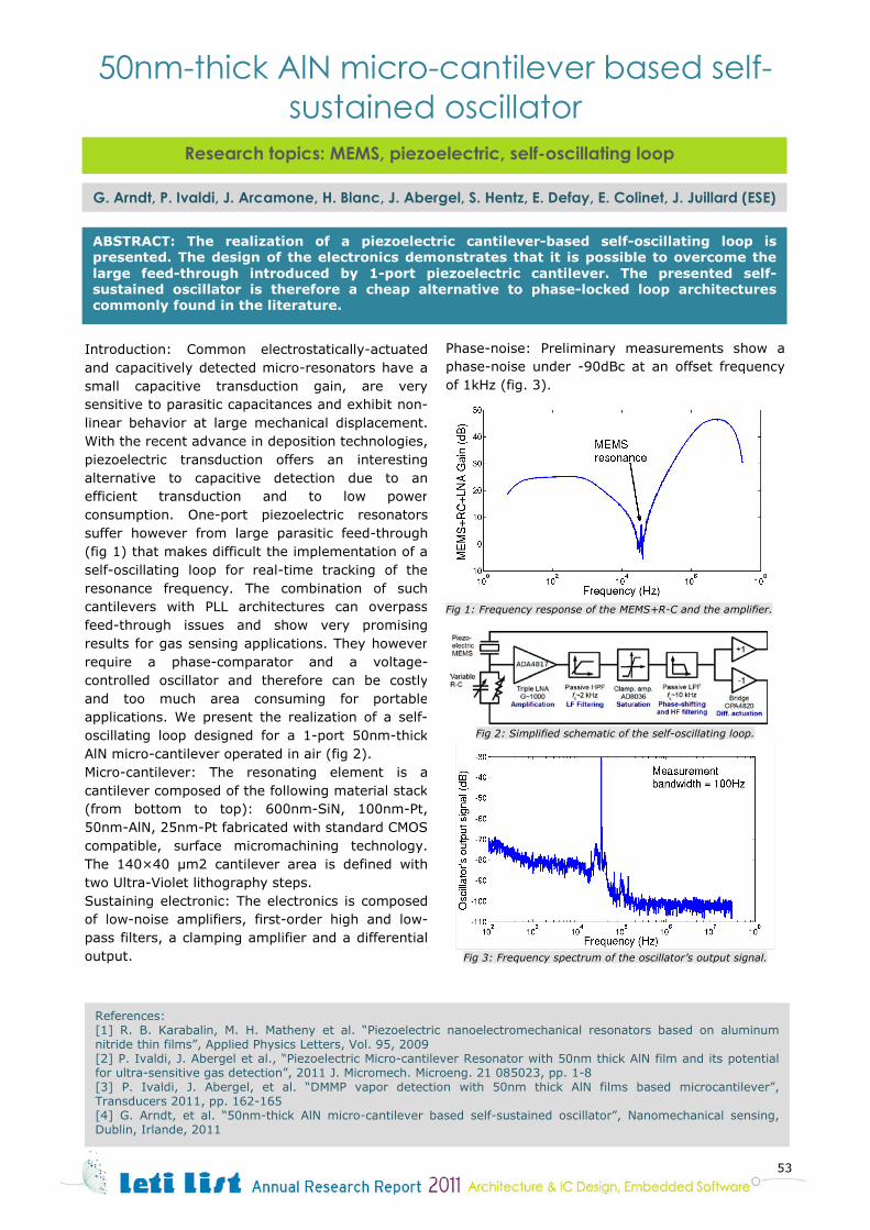
53
50nm-thick AlN micro-cantilever based self-sustained oscillator
Research topics: MEMS, piezoelectric, self-oscillating loop
G. Arndt, P. Ivaldi, J. Arcamone, H. Blanc, J. Abergel, S. Hentz, E. Defay, E. Colinet, J. Juillard (ESE)
ABSTRACT: The realization of a piezoelectric cantilever-based self-oscillating loop is presented. The design of the electronics demonstrates that it is possible to overcome the large feed-through introduced by 1-port piezoelectric cantilever. The presented self-sustained oscillator is therefore a cheap alternative to phase-locked loop architectures commonly found in the literature.
Introduction: Common electrostatically-actuated and capacitively detected micro-resonators have a small capacitive transduction gain, are very sensitive to parasitic capacitances and exhibit non-linear behavior at large mechanical displacement. With the recent advance in deposition technologies, piezoelectric transduction offers an interesting alternative to capacitive detection due to an efficient transduction and to low power consumption. One-port piezoelectric resonators suffer however from large parasitic feed-through (fig 1) that makes difficult the implementation of a self-oscillating loop for real-time tracking of the resonance frequency. The combination of such cantilevers with PLL architectures can overpass feed-through issues and show very promising results for gas sensing applications. They however require a phase-comparator and a voltage-controlled oscillator and therefore can be costly and too much area consuming for portable applications. We present the realization of a self-oscillating loop designed for a 1-port 50nm-thick AlN micro-cantilever operated in air (fig 2). Micro-cantilever: The resonating element is a cantilever composed of the following material stack (from bottom to top): 600nm-SiN, 100nm-Pt, 50nm-AlN, 25nm-Pt fabricated with standard CMOS compatible, surface micromachining technology. The 140×40 µm2 cantilever area is defined with two Ultra-Violet lithography steps. Sustaining electronic: The electronics is composed of low-noise amplifiers, first-order high and low-pass filters, a clamping amplifier and a differential output.
Phase-noise: Preliminary measurements show a phase-noise under -90dBc at an offset frequency of 1kHz (fig. 3).
Fig 1: Frequency response of the MEMS+R-C and the amplifier.
Fig 2: Simplified schematic of the self-oscillating loop.
Fig 3: Frequency spectrum of the oscillator’s output signal.
References: [1] R. B. Karabalin, M. H. Matheny et al. “Piezoelectric nanoelectromechanical resonators based on aluminum nitride thin films”, Applied Physics Letters, Vol. 95, 2009 [2] P. Ivaldi, J. Abergel et al., “Piezoelectric Micro-cantilever Resonator with 50nm thick AlN film and its potential for ultra-sensitive gas detection”, 2011 J. Micromech. Microeng. 21 085023, pp. 1-8 [3] P. Ivaldi, J. Abergel, et al. “DMMP vapor detection with 50nm thick AlN films based microcantilever”, Transducers 2011, pp. 162-165 [4] G. Arndt, et al. “50nm-thick AlN micro-cantilever based self-sustained oscillator”, Nanomechanical sensing, Dublin, Irlande, 2011

54

55
Embedded Software
Real-Time Software
Parallel Software
Middleware for Sensor Networks
5

56
CHRONOSCOPE: a Static Analysis Tools for C multitask realtime applications
Research topics: Static analysis, multitask real-time application, C language
Selma Azaiez, Belgacem Ben Hedia, Thierry Goubier, Vincent David ABSTRACT: The safety of multitask and realtime applications relies on the respect of several properties (e.g. absence of deadlock, atomicity, respect of temporal constraints, etc.). Verifying such properties from the source code requires a complex analysis platform that is able to identify code patterns semantic and to apply the appropriate verification process.
CHRONOSCOPE is an action initiated by IRSN (Institut de Radioprotection et de Sûreté Nucléaire) and CEA/DACLE/LaSTRE. Its goal is to reason about design rules that have to be respected within source code and ensure the absence of errors. For instance, race conditions which are common errors in parallel programming, lead to unintended non-determinism and erronous results. In practice, race conditions and deadlocks are avoided by applying a design rule which consists on protecting access to shared memory with locks and imposing a partial order on lock acquisitions. To date, existing static analysis tools are developed to check errors in sequential programs (e.g. ASTREE, PolySpace, CAVEAT, etc.) or are dedicated to a single specific property such as absence of deadlock.
Figure 1. CHRONOSCOPE levels of analysis The project started on establishing a list of design rules that ensure the safety of multitask realtime applications by respecting properties such atomicity, absence of deadlock, respect of temporal constraints, etc. Properties verifications were classified within 5 levels of analysis (cf. Fig.1.). In each level, models are extracted from the source code and several rules are verified by different analyzer tools.
Analyser tools are activated depending on identified code patterns (e.g. how tasks are created, what communication and synchronization patterns are used: producers/consumers or readers/writers, etc.). Hence, the analysis platform has to be modular to allow such flexibility. Moreover, as analyzed applications are implemented in C language, it has to be based on a strong C parser. Frama-C has been adopted as a basis for our analysis platform. It actually provides all needed features for Level 0 analyses. Using different tools and different techniques for properties analysis complicate the validation process and a high expertise is required for each type of property. In [1], we propose a pattern-based approach to harmonize the validation process. We introduce the property analysis pattern which provides the analysis process according to the code pattern identified within the source code and the property to verify. A dedicated formalism was proposed to describe it. This approach provides more generality than existing ones. It can be applied for different systems using different languages. Users can plug-in different language parsers and provide the corresponding API semantics. This approach also allows knowledge capitalization by explicitly defining the verification and transformation processes. Finally, this year was also dedicated to study atomicity verification process which is stronger than simply checking the absence of race conditions. Indeed, either checking that access to shared memory is protected; atomicity imposes that order of read and write actions ensures the coherency of the shared data.
References: [1] S. Azaiez, B. Ben Hedia, V. David, "Extracting and Verifying Viewpoints Models in Multitask Applications", in Proceedings of The Third International Conference on Advances in System Testing and Validation Lifecycle, VALID 2011

57
From Model-Based to Real-Time Execution of Safety-Critical Applications
Research topics: real-time, model-based, code generation
Simon Bliudze, Xavier Fornari (Esterel Technologies) and Mathieu Jan ABSTRACT: Developing safety critical real-time systems and ensuring properties such as deterministic behaviour is a challenging task. Automatic transformations from synchronous modelling languages to RTOS are required for the development of real-time applications without compromising the guarantees of their safety. We present an automatic transformation from SCADE to the OASIS safety-oriented real-time execution platform.
Various domains, such as the automotive or avionic industries, develop increasingly complex real-time systems. Model-based approaches have been proposed to specify requirements of such systems and design them. Such design environments allow modelling and simulation of applications as well as generation of qualifiable/certified code. Generated code can then be compiled and run on various Real-Time Operating Systems (RTOS). Classical RTOS are based on an event-triggered approach for the execution of applications and do not provide sufficient predictability and analyzability: the deterministic behaviour of an application cannot be ensured prior to its execution.
The goal of the OASIS approach [1] is to build safety-critical real-time systems where the system behaviour is independent from the asynchrony that is allowed during the execution of an application. Therefore and by construction, OASIS is a complete answer to demonstrate the system timeliness: all timing constraints of all activities are clearly expressed in the design phase and can be formally proven to satisfy (or not!) the capacities of the hardware support. SCADE is a synchronous language derived from Lustre and implemented in the Esterel Technologies SCADE Suite model-based development environnement dedicated to critical embedded software.
To the best of our knowledge, few connections exist between synchronous modelling languages, which allow one to develop applications with certified functional behaviour, and time-triggered execution platforms, which guarantee temporal determinism of systems. The main difficulty in the transformation is computing the logical clocks that define the
temporal behaviour of the agents in such a way as to preserve the functional semantics of the model and optimize the usage of computing resources [2]. One of the main differences between SCADE and OASIS computation models concerns the propagation of data during one computation cycle. In SCADE, data is propagated from inputs to outputs at each computation cycle. In OASIS, all agents read their inputs simultaneously and then simultaneously publish the results of their computation. In order to preserve the computation semantics throughout the transformation, each agent is assigned a specific slot of the computation cycle. Thus, the intermediate values are computed and published by the corresponding agents before the agents that require these values for their computations start their respective cycles. This is illustrated by the figure below with the green lines identifying the original cycles of the SCADE model (level control in water tank) and the dashed arrows - the data flow.
Figure 1. OASIS coordination for a SCADE model.
References: [1] Damien Chabrol, Vincent David, Christophe Aussaguès, Stéphane Louise and F. Daumas, “Determinstic Distributed Safety-Critical Real-Time Systems within the OASIS approach”, Int. Conf. on Parallel and Distributed Computing Systems (PDCS 2005). Phoenix, November 2005. [2] Simon Bliudze, Xavier Fornari and Mathieu Jan, “From Model-Based to Real-Time Executiong of Safety-Critical Applications: Coupling SCADE with OASIS”, ERTS2 2012. February 2012.

58
Scheduling safety-critical real-time bus accesses using Time-Constrained Automata
Research topics: real-time, distributed system, time-constrained automata
Mathieu Jan, Jean-Sylvain Camier and Vincent David ABSTRACT: Assuming that tasks have been allocated on CPUs, the difficulty in distributed real-time systems is to ensure an optimal scheduling of network accesses. We claim that the network scheduling must be generated automatically by an off-line tool chain. We present how we adapted Time-Constrained Automata (TCA) to model communication requirements, in the context of a multi-scale time-triggered execution model.
Distributed architectures are becoming a common target for real-time embedded safety-critical systems, notably in order to enhance their availability. The design and implementation of such systems must be carefully performed. However, the difficulty is to conceive critical functions according to a framework that ensures an optimized scheduling of network accesses, with no help from the application designer. In this work, we focus on the schedulability analysis and scheduling of bus accesses using a Time Division Multiple Access (TDMA) approach for time-triggered real-time systems. TDMA divides the global time into a sequence of time slots, each of them is assigned to an unique CPU so that no network collision can occur. We assume that tasks have been allocated on CPUs of a distributed system. The schedulability analysis of a simple TDMA protocol (periodic) has already been studied by the research community. We consider the problem of scheduling bus accesses made, not by periodic tasks, but by tasks whose timing behavior are specified using Time-Constrained Automata (TCA) model [1]. Using such a task model, the behavior of tasks are modeled by automata and constrained by time intervals. This is a more expressive task model than the periodic task model.
Our first contribution is to show how we adapted the TCA model to express timing-constraints on data exchanges for a multiscale time-triggered execution model [2]. Applied to a network, the semantic of the four kinds of nodes of the TCA model are the following: • An Afterd node constrains the exchange of a data item to start after the date d.
• A Befored node constrains a data item to be available for consumers’ tasks before the date d. • A Syncd node is a combination of an Afterd and a Befored nodes. • A No node imposes no temporal constraints on data exchanges.
We further optimize the computation by taking into account possible differences between producers, consumers and any temporal behavior of the considered communication mechanisms. Our second contribution is then to transform requirements on data exchanges expressed using TCA into a linear programming problem. We then generate the TDMA scheduling of bus accesses that fits the description of data exchanges requirements in TCA. We show that the proposed approach can be fully integrated in an off-line tool chain. Figure 1 shows the verification of the on-line fulfillment of the off-line generated network schedule of a sample application (speed regulation of a vehicle).
Figure 2. Generated and observed TDMA schedule.
References: [1] Matthieu Lemerre, Vincent David, Christophe Aussaguès, Guy Vidal-Naquet, “An introduction to time-constrained automata”, 3rd Interaction and Concurrency Experience Workshop (ICE’10). June 2010 [2] Mathieu Jan, Jean-Sylvain Camier, Vincent David, “Scheduling safety-critical real-time bus accesses using Time-Constrained Automata”, 19th Conference on Real-Time and Network Systems. September 2011.

59
Method and tools for mixed-criticality real-time applications within PharOS
Research topics: Safety-critical systems
M Lemerre, E Ohayon, D Chabrol, M Jan, M-B Jacques
ABSTRACT: PharOS is a complete set of tools to design, implement and execute hard real-time real-time systems on embedded platforms, such as control and command systems found in automotive embedded systems. We present here the features of PharOS that allows it to address mixed-criticality real-time applications, i.e. applications with safety critical tasks running concurrently with non-critical tasks.
Over the last decades, the number of electronic equipments embedded in complex systems such as automotive vehicles or airplanes has increased in drastic proportions. At first, system architects used to embed one computing unit per functional system, which resulted in large distributed and heterogeneous real-time systems. The current number of equipments makes this approach no more sustainable, mainly due to its high costs. As a result the trend is to integrate several (possibly unrelated) applications on fewer computing units, resulting in what is called a mixed-criticality system. This integration raises however a number of issues, such as: • efficiently and securely sharing resources (and
especially CPU time) between these applications; • providing the same degree of isolation than
achieve when using separate computing units; • combining different real-time paradigms and
APIs; • handling multicore computing units, that are
becoming the usual solution of the chip designers to increase performances.
PharOS is the system that we built to address these problems. PharOS is a complete set of tools to design, implement and execute real-time systems on automotive embedded platforms, comprising a compiler and offline analysis and code generation tools, with a safety-oriented kernel. The keystone of this approach is a dynamic time-triggered methodology that supports full temporal isolation without wasting CPU time. This relies on a rich model of tasks that accurately describes the task constraints, and admits an optimal dynamic scheduling algorithm. Moreover, it allows exact feasibility analysis, which avoids wasting CPU time
by oversizing the time resources for the tasks. The task model is automatically extracted from the application code written in PsiC, a superset of C with statements for inter-task communications and timing annotations, that enforces isolation between the tasks.
Automatic translation from PsiC into the PharOS task model
Furthermore, PharOS guarantees the determinism of the application despite the parallel execution. This provides a behavioral isolation between the tasks, which is a unique feature of PharOS. In addition, memory isolation is handled through automatic off-line generation of fine-grained memory protection tables used at runtime. These isolation mechanisms are building blocks for the support of mixed-criticality applications. Several further extensions expand the support for mixed-criticality within the system. These extensions include fault recovery, support for the cohabitation of event-triggered with time-triggered tasks, and paravirtualization of other operating systems.
References: [1] Matthieu Lemerre, Emmanuel Ohayon, Damien Chabrol, Mathieu Jan and Marie-Bénédicte Jacques, “Method and Tools for Mixed-Criticality Real-Time Applications within PharOS”, Proceedings of AMICS 2011: 1st International Workshop on Architectures and Applications for Mixed-Criticality Systems

60
New approaches to low-level abstract interpretation for execution time analysis
Research topics: Worst / Best-Case Execution Time, abstract interpretation, models
S. Louise, A. Dkhil
ABSTRACT: Execution time knowledge is a requirement in embedded software, specifically for scheduling validations and for real-time constrains verifications. Execution time analysis aims at identifying all possible execution path of a given program and predicting the actual execution time through system architecture and execution process modeling. In this work, we present a new proposal for low level modeling of branch predictors.
Execution Time knowledge is a requirement for scheduling theories, including multi-processor scheduling optimization, and for verification of real-time constraints. That means tools for execution time analysis have a growing role to play in embedded software development tool-chains. Of course, one naïve approach is to make a sampling of empirical execution times. Nonetheless, in some corner cases, this approach is insufficient for accurate scheduling analysis, and is inconsistent with hard real-time timing analysis requirement. Indeed, in the later case, guarantees and proofs must be provided on the execution time boundaries and such guarantee cannot be shown on execution time sampling. Execution time analysis is an important field of research, with still on-going challenges to face: the ever changing technological landscape of processor architecture, introducing new features on a regular basis; the non-deterministic behaviors of several processor feature like cache memories, pipeline stalls, and so on; and finally the limits of decidability of programs in the general case. Therefore only a subclass of program are formally analyzable, and on of the goal of execution time analysis is to expend the field of automatic analysis as far as possible, and being able to include as accurate an execution model as possible (e.g. taking into account fully preemptible scheduling policies). Two main fields of execution time analysis can be distinguished: the high level analysis which wants to analyze all the possible execution paths of a given program, and the low level analysis which use these results with a mathematical model of the system that execute the program in order to evaluate the possible execution time as accurately as possible. Our works lye into this low level analysis, as some
earlier works dealt with cache memory modeling for low level analysis [1,2]. We used the same kind of formalism (based on linear algebra and a Markov model) to model branch prediction behaviors. A first extended paper was published in WCET Workshop at ECRTS 2011 (the main workshop of the domain) for the “simple” saturating counter based branch predictor [3]. The main principle is to extend the automaton of the branch predictor (fig. 1) onto an abstract state automaton which takes into account that under static analysis some branch predictions have unknown outcomes (fig. 2).
Figure 3 Simple branch predictor principle (based on a 2 bit saturating counter)
Figure 4 Associated abstract space (model)
The associated operators were defined and a first evaluation of branch prediction related timing was done on several standard benchmark programs. A work in progress paper was published in RTSCA conference and CPSNA workshop with a first step to take complex history based branch predictors into account [4].
References: [1] S. Louise, “WCET safe upper-bound computations for hard real-time tasks, for systems using cache memories”, PhD thesis, université Paris-sud, centre d'Orsay, December 2001 [2] “S. Louise, A preliminary study of WCET for a non deterministic cache policy”, ECRST'2009 WiP, Dublin, pp 17–20 [3] S. Louise, A. Dkhil, “Branch prediction related WCET with a Markovian Model”, WCET workshop, Porto, 2011 [4] S. Louise, et al., “Improving branch prediction related WCET abstract interpretation”, RTCSA'11 WiP & CPSNA 2011

61
Task Migration Mechanisms for Hard Real-Time Distributed Systems
Research topics: real-time, distributed system, schedulability
T. Megel, M. Jan, V. David and C. Fraboul (IRIT, Toulouse) ABSTRACT: In the context of distributed non real-time systems, several mechanisms have been proposed to migrate tasks in order to reduce their freeze time. In this work, we focus on distributed hard real-time systems. We present four techniques: Total Copy, Prefetch Precopy, Prefetch Postcopy and Mixed Copy, that take advantage of the static description of the temporal behavior of hard real-time tasks.
Task migration is a mechanism that has been well studied in the past decades in distributed non real-time systems. The main goal of the various proposed techniques is to reduce the so called freeze time of a task, i.e. the time interval during which a task cannot be executed due to on-going migrations. Allowing a freeze time in a real-time system could make the system less predictable and could lead to miss some deadlines. Nowadays, critical real-time systems such as automotive and avionic control system applications are often distributed. The reliability of these systems is important: even if a hardware failure occurs such as a node crash and therefore the lost of all the tasks executed on this node, critical tasks must still be executed to guarantee availability. One of the most prevalent strategies to achieve, at best, the graceful degradation of distributed hard real-time system is to handle with a set of replicas of critical tasks, using dynamic replication capability when failures occur. The design of guaranteed migration mechanisms for hard real-time system, with predictability properties, is therefore needed.
We show how we can build adapted migration mechanisms to the context of distributed hard real-time systems [1][2]. Such systems assume the static description of both their temporal and logical behavior, i.e. the real-time constraints associated to each task and the possible execution paths of tasks are known. We present four migration techniques that show this claim: Total Copy, Prefetch Copy, Prefetch Postcopy and Mixed Copy. The Figure illustrates the smallest, current and largest interval of transfers of the Mixed Copy strategy. Mixed Copy (see Figure 1) consists in copying the memory required by the next job after migration deadline first, then transfer all remaining
memory whether the task has been resumed in the destination node or not. In addition, this static description of possible execution paths allows the identification of memory areas that are required (in read, write or execute access) by each job of a given hard real-time task. We use this relationship to efficiently organize data transfers on the network according to different strategies (Prefetch Pre and Postcopy policies) and temporal constraints associated to jobs. We formalize the various temporal constraints that describe the feasibility conditions of migrating a task whatever the migration deadline is. Specific additional tasks are used to implement in each node the migration policy of tasks. These tasks are integrated to the existing task set to verify CPU and network schedulability.
Figure 5. Mixed copy strategy for task migration.
References: [1] Thomas Megel, Mathieu Jan, Vincent David, Christian Fraboul, “Task Migration Mechanisms for Hard Real-Time Distributed Systems”, 17th Real-Time and Embedded Technology and Applications Symp. (RTAS). WiP session. April 2011. [2] Thomas Megel, Mathieu Jan, Vincent David, Christian Fraboul, “Evaluation of Task Migration Mechanisms for Hard Real-Time Distributed Systems. 19th Conference on Real-Time and Network Systems. September 2011.

62
Specialized OS for highly dependable hard real-time systems
Research topics: Parallel Execution model, OS, nuclear safety compliance
S. Louise, M. Lemerre, C. Aussaguès, V. David
ABSTRACT: The OASIS model provides a quantum leap in ease of design and programing over old state of the art methods for nuclear power Instrumentation and Control (I&C) systems. The requirements that are enforced by very strict standards and rules offer very few latitude for a generic OS. In this work we show how we designed and programed a generic OS for the execution support of the ΨC language that conform to the strict standard ISO-60880 for nuclear safety, but still get good performance within these constrains.
Instrumentation and Control programmed systems for nuclear power plant follow very strict standards (in conformance with the associated risks of such facilities). These standards, being very conservative, make some serious limits on the use of a standard OS with these systems. The OASIS kernel is then an achievement, not because as an OS and execution support for OASIS applications it has some extraordinary feature or implements a breakthrough in OS design, but because it mix a good step up from usual I&C nuclear power system design by allowing real parallel tasks, and a conservative enough implementation, with a sane design for safety. The OASIS kernel [2] is a generic (i.e multi-applications) OS that implement a specialized support of the language associated with the OASIS model [1]: the ΨC language. It provides a very strict and strong memory protection scheme, it contains provably no dead code, and make some continuous auto-test of the application regarding its logical and time related behavior. OASIS has two main layers (see figure 1):
• the micro-kernel which acts as the time manager, schedules the real-time tasks and act as a watch-dog for any timing overrun,
• the agent kernel manages communication between tasks, and perform auto-tests on the logical behavior of each real-time task under its supervision.
Since only the micro-kernel is non-preemptible, the overall system can reach good performance inspite of its safe design (and inspite of the strict memory
protection scheme), enabling to switch between task in less than 2 µs in the worst case while doing 4 MMU context switch meanwhile, on a relatively old Pentium M processor.
Figure 6 – The layered architecture of an OASIS application: the OASIS kernel has 2 parts (µ-kernel and agent-kernel) defining a strict memory protection scheme that depends on the associated task context. Transition between layers are done through carefully managed service calls The kernel was used in the industrial product QDS, made by Areva-NP for the new generations of nuclear power plants, and the QDS allows for a generic real-time display with a full featured HMI (mouse, keyboard, touchscreen, modern graphic interface) for emergency shutdown monitoring [3].
References: [1] S Louise, V David, J Delcoigne, C Aussagues, OASIS project: deterministic real-time for safety critical embedded systems, 10th ACM SIGOPS European Workshop (rank B), Saint-Emilion, France, September 2002 [2] S Louise, M Lemerre, V David, C Aussagues, The OASIS kernel: a framework for high dependability real-time system, 13th IEEE International High Assurance Systems Engineering Symposium [3] V David, C Aussaguès, S Louise, P Hilsenkopf, B Ortolo, C Hessler, The OASIS based qualified display system, American Nuclear Society International Topical Meeting on Nuclear Plant Instrumentation, NPIC&HMIT 2004

63
Probabilistic parameters of conditional task graphs
Research topics: Parallel computing, conditional task graph, probabilistic release/delivery times, multiprocessor scheduling
S. Carpov, J. Carlier (UTC Heudiasyc), D. Nace (UTC Heudiasyc), R. Sirdey ABSTRACT: This work deals with the problem of determination of probabilistic parameters for tasks in a series-parallel conditional task graph. Such problematic is encountered in the context of parallel computing when dealing with conditional precedence constrained parallel tasks on a multi-core machine. We focus on the calculation of two probabilistic parameters: the release dates and the delivery times. An algorithm for computing these parameters is proposed.
A task graph model, also known as directed acyclic graph (DAG), is used to represent algorithms which have to be executed on a parallel computing system. A multitude of methods have been proposed in the literature to deal with the DAG scheduling on multiprocessor systems having as objective the completion time minimization. The above methods use different parameters which are defined for the DAG’s tasks. Two important parameters are the release date (head or top level) and the delivery time (tail or bottom level) of a task. These parameters are used in task selection rules of list scheduling algorithms. Another important parameter for a task graph is the minimal execution time (or the critical path) which is the completion time obtained when no constraint is imposed on the number of available processors (i.e. when the number of processors is considered to be unlimited). The minimal execution time is a lower bound for the completion time of the general multiprocessor scheduling problem and it is used in tree search algorithms (e.g. branch and bound methods) to reduce the search space. The task graph model lacks of expressivity which limits its use in many practical situations. A first drawback is the hypothesis that task execution times are constant. In reality, they are variable and depend on several factors (caching, branch prediction mechanisms). A second disadvantage is the absence of tools for modeling conditional branches which are widely employed in programs. A conditional branch is a special task, such that only one of its successors is executed (in function of a condition depending on the input data for example). The case of variable task durations is known in the literature on probabilistic PERT scheduling and on stochastic DAG scheduling. The literature on task graphs with conditional branches
is scarce and mainly consists in methods for allocating and scheduling them onto multiprocessor systems. The goal of this study is to define probabilistic parameters for task graphs with conditional branches. Roughly speaking, a conditional task graph (CTG) is a DAG in which certain edges have an execution probability. In Fig.1 a CTG is illustrated. In this CTG the probability of tasks 5,7,8 and 9 execution is 0.6 for example. An algorithm for finding probabilistic heads and tails for each vertex of a series-parallel CTG is proposed. The algorithm has a pseudo-polynomial complexity. The execution time of the algorithm depends on the sizes of the domains of definition of the discrete random variables used to represent the heads and the tails. At the price of less precise results the execution time of the algorithm can be reduced in order to be able to use it for graphs encountered in practice. For the example illustrated in Fig.1 the critical path value (head of task 11) is 13 with probability 0.32, 14 with prob. 0.08, 17 with prob. 0.48 and 18 with prob. 0.12.
Figure 1. Conditional task graph example.
References: [1] S. Carpov, J. Carlier, D. Nace, R. Sirdey: “Probabilistic Parameters of Conditional Task Graphs”. NBiS 2011, pp. 376-381, 2011.

64
Task Ordering and Memory Management Problem for Degree of Parallelism Estimation
Research topics: task scheduling, memory management, parallel processor
S. Carpov, J. Carlier (UTC Heudiasyc), D. Nace (UTC Heudiasyc), R. Sirdey
ABSTRACT: This study is devoted to the problem of estimating the achievable degree of parallelism for a parallel algorithm with respect to a bandwidth constraint. In a compiler chain for embedded parallel microprocessors such an estimation can be used to fix an appropriate target for parallelism reduction “tools”.
In this work [1], we investigate a series of problems related to efficient memory bandwidth management in embedded parallel processor architectures. In particular, we are interested in estimating the memory bandwidth required for the sequential execution of a parallel algorithm so as to estimate the number of tasks which may execute in parallel with respect to an external memory bandwidth constraint. In a compiler chain proceeding by parallelism reduction, such estimation can be used to fix an appropriate target for the degree of parallelism. This estimation can also be used within an Algorithm-Architecture Adequation framework to perform an initial assessment. Let us consider an embedded parallel processor architecture which consists of many processing cores which share a common memory space. The system, in which this processor is used, has an external memory for storing application data and instructions. External memory locations are accessed without direct core involvement, i.e. it only initiates and finishes the data transfers. In this context, a typical bottleneck for many algorithms is the external memory access bandwidth, which must be carefully managed in order to keep the processing cores busy enough. An algorithm is composed of a set of tasks that are using external memory data. The data loading time is variable because several data could be loaded two or more times in function of the caching strategy. In this study, we propose a method to estimate the achievable degree of parallelism for an algorithm constrained by the external memory bandwidth, that is the ratio Λ/λ between the external memory bandwidth Λ to the average bandwidth λ required by an optimal sequential execution of the
algorithm. We suppose that we are dealing with parallel algorithms, thus their intrinsic structure in terms of parallelism is not an issue, only the limitations of the chip (here, in terms of external memory bandwidth) influence the estimation. The average bandwidth λ is defined as the total amount of data divided by the total execution time. It is straightforward to see that the average bandwidth is proportional to the amount of data loaded from the external memory, thus loading less data will reduce the bandwidth. Informally, our problem consists in task ordering and memory management for an algorithm, so as to minimize the number of memory accesses. We prove the NP-hardness of this problem and introduce a polynomial special case. We propose a branch and bound procedure for the general case along with computational results interpretation demonstrating its practical relevance. An example optimal task processing order which minimized the total number of external memory accesses is represented in Fig.1. The used application is an M by N image convolution with 3x3 kernel.
Figure 1. The optimal order of task processing for an M by N image convolution.
References: [1] S. Carpov, J. Carlier, D. Nace, R. Sirdey: “Task Ordering and Memory Management Problem for Degree of Parallelism Estimation”. COCOON 2011, Lecture Notes in Computer Science, vol. 6842, pp. 592-603, 2011.

65
References: [1] F. Galea and B. Le Cun. ”A Parallel Exact Solver for the Three-Index Quadratic Assignment Problem”. In PCO'11 as part of the 2011 IEEE IPDPS'11, pp. 1935--1944, Anchorage, USA, May 2011. [2] F. Galea and B. Le Cun. ”Bob++ : a framework for exact combinatorial optimization methods on parallel machines”. In PGCO'2007 as part of the HPCS'07 and in conjunction with The 21st European Conference on Modeling and Simulation (ECMS 2007), pp. 779--785, Prague, Czech Republic, June 2007.
Exact solution of a difficult combinatorial optimization problem using parallelism
Research topics: Parallelism – Combinatorial Optimization – Operational research
F. Galea, B. Le Cun (Université Versailles St Quentin)
ABSTRACT: We implemented a branch-and-bound–based exact algorithm for the Three-Index Quadratic Assignment Problem (Q3AP) on multicore processors. Our parallel implementation has two levels of parallelism: the tree search procedure uses the Bob++ parallel search framework. The lower bound computation uses the SIMD extensions of modern processors.
Q3AP is an extension of the Quadratic Assignment Problem (QAP), which is well known in the combinatorial optimization community. While QAP is considered a difficult problem, Q3AP is even more difficult. Different industrial problems can be formulated as a Q3AP problem, in fields such as wireless networking. The Q3AP may be described as follows: consider a facility-location problem with N facilities and N locations, where in addition to assigning facilities to locations we also want to assign N managers to the N locations. A solution to this problem is a set of N triplets (manager, facility, location), where all the managers, facilities and locations are assigned one-to-one. The cost of a solution is the sum of Lijk linear costs for each of the chosen (i, j, k) assignments (i.e., the sum of the Lijk*xijk products for placing manager i and facility j to location k), plus the sum of Cijklmn quadratic costs for each ((i, j, k), (l, m, n)) pair of assignments (i.e., the quadratic cost Cijklmn*xijk*xlmn for placing manager i and facility j to location k, and manager l and facility m to location n).
The problem was exactly solved [1] using a parallel branch-and-bound procedure in the Bob++ parallel search framework we developed [2]. Multi-core parallelism is used to accelerate the tree spanning by exploring different subtrees in parallel. Table #1 shows typical run times depending on the number of used cores.
Table 1.: run times (in seconds) of our solver using different numbers of cores on a multi-core workstation.
The SIMD extensions of the processor (Intel SSE2) were used to accelerate the lower bound computations in the tree nodes. Table #2 compares the run times of the bound procedure implemented with and without SSE.
Table 2.: run times (secs) and speedups for the lower bound implementation using SSE (vector) vs. a scalar implementation. These parallelization techniques are suitable for use on a large variety of problems. We are currently developing a heuristic solver for a place and route problem on a 48-cores server.

66
New execution model for Chip Multi-Processors
Research topics: Execution model, parallelism, OS accelerators
S. Louise, V. David
ABSTRACT: As multi-core architectures become the standard for embedded systems, it is widely acknowledged that parallelism management for parallel architecture and for embedded application is difficult. We present a new approach to heterogeneous multi-core systems to provide a simple multi-task, multi-threaded execution model for such an architecture, by introducing an execution unit specialized in parallelism management on the front-end core.
The era of ever increasing single-core performance is over; the new Moore's law nowadays roughly translates as: the number of available cores on an up-to-date chip double every 18 to 24 months. Nonetheless, programming multicore architectures is a difficult task for the embedded programmers, because usual HPC programming scheme like MPI or OpenMP do not fit well with the usual applications of the embedded world: these application require a very light-weight OS and library support and a very dynamic execution scheme in order to fit performance with execution time requirement and optimizing power consumption within these constrains. The main principle of our approach is to start from a simple observation: parallel programming is difficult, whereas the dynamic parallel execution of instructions with superscalar architectures was a very efficient way to keep a simple programming model (sequential programming), with the processor using dynamical knowledge of the execution to optimize the parallel issue and execution of single instructions. Our approach involves a single core processor with several Auxiliary Processing Unit cores (APU) (fig. 1), to execute dynamically tiny processing kernels. The APU are execution units for High-Performance Computations and are limited mostly by the limits of Amdahl's Law, hence the parallelism exploitation is better if a wide range of parallel kernel coarsening level is possible. That means that if fine granularity parallel kernel can be used efficiently, then the kernel and core management time must also be tiny, by at least an order of magnitude with regards to the minimum execution time of the parallel kernel executed on an APU [1]. We showed how to define a specialized execution unit —called Auxiliary Control Unit (ACU)— of the front-end processor that manage the APU and act
as an OS accelerator for dynamic parallelism optimization. If implemented entirely in hardware, such a unit can manage the execution of APU within less than 15 cycles at 500MHz on a 65nm process. That allows for very tiny kernel management, and a very wide level of parallelism management. The parallel task management (in the sense of a multitask OS, ala Unix) is still done by the OS, but the ACU indicate points when switching tasks can be more efficient, and manage kernel execution dynamically without help from the main OS [2].
Figure 1. General architecture principle
Figure 2. ACU architecture
Future works include refining the programming model on one hand, and on the other hand to scale the proposed architecture to many-core system, which would take an advantage in 3D stacking of processing cores, on-chip memory, and defining a clever interconnection scheme between them.
References: [1] F. Calcado, S. Louise, D. Vincent, “Efficient use of processing cores on heterogeneous multicore architecture, International Conference on Complex, Intelligent and Software Intensive Systems”, IEEE Workshop on Multi-Core Computing Systems, March 2009, Fukuoka, Japan, pp 669-674 [2] S. Louise, et al., “A single processor approach for loosely synchronized execution of parallel flows on heterogeneous multicore”, ICCS'11, Singapore, May 2011

67
Flexible and Performing Kernels Dynamically Generated with deGoal
Research topics: dynamic compilation, processing, embedded software, HPC
H.P. Charles, D. Couroussé, Y. Lhuillier ABSTRACT: deGoal is a tool designed to build fast and portable binary code generators, in order to improve the performance of CPU-bounded applications. It currently supports the STxP70 core of the P2012 platform, ARM processors used in the embbeded domain, and Nvidia GPUs (PTX) used for High Performance Computing.
Modern compilers embed a lot of optimization knowledge to make the most of the target architecture. Such compilers are however unable to exploit runtime information, in particular the data to process, because code generation is done before the application has started its execution. deGoal (http://www.degoal.org) is a tool designed to tackle this issue, i.e. the generation of machine code that depends on the data to process. It is different from JIT compilers (Java or LLVM), because it is not based on an intermediate representation (no bytecode), has a low memory footprint, puts a strong focus on hardware portability and is faster than any code generator. Using deGoal the developer is able to embed tiny specialized code generators, called "compilettes", in an application. Such a compilette will be able, at runtime, to generate the code of a processing kernel. The generated kernel is optimized depending on the data to process, the target processor and its instruction set. deGoal currently supports the STxP70 core of the P2012 platform, ARM processors used in the embbeded domain, and Nvidia GPUs (PTX) used for High Performance Computing (HPC). On the P2012 platform, we demonstrated the effectiveness of deGoal on matrix processing and on the implementation of a memory allocator. Figure 1 presents the speedup obtained on matrix multiplication. It compares a static version compiled using the platform compiler with full optimization and an implementation using deGoal. Our implementation provides a performance increase of 111% using VLIW instructions, and 56% without VLIW support for square matrices of
256 elements. The binary code generated by deGoal is not sensitive to compiler's options, and provides good performance whatever the size of the input matrices. The memory allocator we implemented is an optimized version of dlmalloc. Using deGoal we managed to bring extra flexibility to the initial static implementation without degrading performance. We also exploited runtime information to adapt the behavior of the allocator to the memory properties of the application. The performance of the allocator could then be improved by an max./average speedup of 56%/35%. This work is funded by the SMECY project. On Nvidia GPU accelerators, thanks to deGoal our compilette is able to specialize the code on the fly. Our actual experimentations use data size information to produce more efficient code by inserting stride and fixed addresses and also by removing unnecessary tests. This work is funded by the european ITEA2 H4H project.
Figure 1. Speedup results of the matrix multiplication on the STxP70-v4 core.
References: [1] Charles, H.-P. (2012), Basic Infrastructure for Dynamic Code Generation, in Henri-Pierre Charles; Philippe Clauss & Frédéric Pétrot, ed., workshop "Dynamic Compilation Everywhere", in conjunction with the 7th HiPEAC conference. [2] Lhuillier, Y. & Couroussé, D. (2012), Embedded System Memory Allocator Optimization Using Dynamic Code Generation, workshop "Dynamic Compilation Everywhere", in conjunction with the 7th HiPEAC conference.

68
New Programming Technologies for Multi-core Embedded Systems
Research topics: Multi-core, toolchains
S. Bensalem(Verimag), D. Couroussé, J. P. Krimm, Y. Lhuillier, J. Mottin, F. Pacull
ABSTRACT: SMECY is an ambitious European initiative (Artemis project) involving 27 partners across 9 countries to help Europe to have a leader role in multi-core domain by developing new programming technologies enabling the exploitation of architectures offering hundreds of cores.
The SMECY project envisions that recently emerged multi-core technologies will rapidly develop to massively parallel computing environments which, due to improved performance, energy and cost properties, will extensively penetrate the embedded system industry in a few years. This will affect and shape the entire business landscape The mission of this project is to develop new programming technologies enabling the exploitation of many (100s) core architectures. The goal of this ARTEMIS project is to launch an ambitious European initiative (27 partners across 9 countries) grouping together tools providers, platform providers and partners developing applications more and more resources demanding. The approach of the SMECY project [1] is to take into account for designing the tool chain of both the specificities of the hardware platform and the characteristic (in terms of possible parallelism) of the applications. Indeed, we are convinced that it is hopeless to design a single generic multi-purpose tool chain (grail quest since the apparition of the first parallel machine). To deal with this approach we have organized the project in clusters, each of the clusters targeting a given type of application on a specific platform. We have 3 types of applications: - radar applications, for which the image processing aspects through matrix computation is the common target. - mobile, wireless and multimedia, for which the power consumption aspect is the key point. - video processing and video surveillance, for which the data stream aspect is taken into account. As shown in the figure 1 the 3 types of applications define the 3 clusters of the project. The 2 first target ST P2012 platform [2] while the 3rd one will
use the EdkDSP platform from UTIA university.
Figure 1 : the 3 clusters of SMECY
Beside the integration of tools, the project has a prospective part to define HW/SW Architecture innovative concepts in order to study and develop new solutions for multi-core architectures, programmability, virtualization, acceleration of parallel execution, and runtime execution support [3]. Some of these mechanisms are intended to be used in the back-end tools in the last year of the project. One of the main goals of the SMECY project is to deliver a common architecture, APIs, and interoperable tools suites for heterogeneous multi-domain architectures. It is therefore critical to propose and adopt a common Intermediate Representation (IR) format that can be the central communication interface between the SMECY tools. In addition this IR should strongly rely on already existing formats in order to capitalize on existing knowledge and to guarantee future exploitation after the end of the SMECY project.
References: [1] F. Pacull, K. Bertels, M. Daněk and G. Urlini , "SMECY:Smart Multi-core Embedded Systems," Special session, in Proceedings 21st Great Lakes Symposium on VLSI Design-GLSVLSI 2011, Lausanne, 2011. [2] A. Basu, J. Mottin and J. P. Krimm, "Compiling Applications for P2012 with BIP Tool Chain," in STMicroelectronics P2012 Developer's conference, Minatec, Grenoble, 1 Dec 2011. [3] Y. Lhuillier and D. Couroussé, "Embedded System Memory Allocator Optimization Using Dynamic Code Generation," in worshop Dynamic Compilation Everywhere, 7th HiPEAC conference , Paris, France, 2011.

69
A coordination middleware for sensor/actuator networks
Research topics: Coordination Middleware, sensor/actuator networks
L.-F. Ducreux, S. Lesecq, F. Pacull
ABSTRACT: A coordination middleware for sensor/actuator networks allows to solve the difficult problems inherent to heterogeneity, asynchronicity and distribution at the system level. This eases the task of the application designers, allowing them to focus on the scenario aspects.
Designing an application involving networks of sensors and actuators is generally a difficult task that requires various competencies: - Driver level skills, to manage the low-level part of the sensor/actuator networks (gateway, communication protocol, etc.); - HMI skills, for defining the actual scenarios and the interactions with the users; - System skills to deal with system aspects such as distribution, concurrency, fault-tolerance, consistency, power management optimizations. The Chaski middleware is well suited for coordination of sensors/actuators networks since it is able to manage and hide the above mentioned difficult issues that are painful to handle at the application level. In addition, it offers a framework to simplify the integration of hardware devices (sensors / actuators). This low layer is then decoupled from the application aspects and may be implemented by specialists. Thus, the application designer only focuses on the scenarios and related interactions and relies, on the one hand, on the properties guaranteed by the middleware and, on the other hand, on the encapsulation of the different sensor/actuator networks. The middleware integrates a coordination mechanism based on rules that allows to first verify that distributed conditions (e.g. set of values returned by sensors geographically distributed and/or states stored in databases) are verified at the same logical time and, in a second time, to trigger a set of actions combined within transactions. In this way, the distributed system evolves from one consistent state to another consistent state [1]. Another property of the middleware is its capability to deploy applications [2] over large-scale
distributed systems.
Figure 1: Application deployment
Indeed, it provides a mechanism that allows, at application launch time, to send to the remote hosts not the code for the software components but a high level description of this latter. This allows the remote hosts to build and instantiate the components according to the basic bricks locally available. This allows taking into account the resources constraints (memory, power consumption, etc.) and adapting each application component to its very own context. Thus, as illustrated in figure 1, an application can be deployed from a central point to heterogeneous hosts belonging to different local area networks with no information about the hardware and software characteristics of these hosts. The Chaski middleware has been used to integrate off-the-shelf heterogeneous sensors/actuators networks with devices coming from different CEA-Leti teams in various scenarios illustrating heterogeneity, auto-configuration and adaptation to the context [3]. The next generation of this middleware will target smaller footprint embedded-systems.
References: [1] François Pacull, Laurent-Frédéric Ducreux, Suzanne Lesecq, Stéphanie Riché, “Consistency and Distributed Sensor Data Processing”, SENSORDEVICES 2011 [2] François Pacull, “Deployment management through on-remote-site dynamic compilation”, Workshop Dynamic Compilation Everywhere held in conjonction with the 7th HIPEAC conference, January 2012. [3] P. D. Berger, J. Willemin, J. F. Christmann, S. Riché, C. Condemine, E. Beigné, L. F. Ducreux, S. Lesecq and F. Pacull, "Autonomous Smart Sensors : From MEMS design to wireless sensor network deployment (focus on Energy harvesting platform and a coordination middleware)", EUROSENSORS 2011

70
Middleware for self-aware Internet of Things
Research topics: internet of things, middleware, autonomic computing, wireless sensor/actuator networks
L. Gürgen ABSTRACT: This research investigates middleware solutions for development, deployment, coordination and management of internet of things (IoT) applications. The middleware offers self-manageability features and follows a service-oriented approach dealing with IoT characteristics such as high dynamicity, heterogeneity, real-time nature, distributed data processing and dependability requirements.
Despite their potential of great economical and societal impact, IoT systems are still not widely deployed. There exist several reasons for this. - In most of the existing solutions, IoT devices (e.g., sensors, actuators) are tightly coupled with a given application. This limits the reuse of the devices for different applications. - Coordination of sensing and acting devices is provided with predefined and static rules in current solutions. This naturally limits the flexibility of applications and their evolution. - Current sensors still need manual configuration, upgrade and monitoring, which is very complex with the increasing scale of the IoT networks. This research explores the scientific and technical challenges raised by the above mentioned issues and proposes a middleware for reusable, scalable, dynamic and autonomic IoT. In particular we address the following questions: - How to describe sensor and actuator devices in a common way so that other devices can discover them automatically? We propose device descriptions [1] that define the capabilities of sensor and actuator devices in order that they are automatically discovered and used by other devices in the network. We define descriptions small in size yet great in extensibility and flexibility, while taking into account existing standards. - How to collect and process sensor data in an energy efficient way? We analyze existing data processing techniques [2] and propose new declarative and distributed processing techniques for scalability and energy efficiency.
- How to deal with the heterogeneity of sensor and actuator devices? By adopting a service oriented approach [3], we provide a homogenous view over various types of devices from different manufacturers. Sensors provide standard means to retrieve their data and actuators declare the actions that they can perform in terms of services. - How to make IoT self-aware so that devices can reason about the context and self-adapt to optimize their quality of service? We define mechanisms to describe and execute user defined rules that characterize the desired behavior of the system in given specific conditions [4]. This leads to a dynamic evolution of ioT systems that can re-configure devices, deploy new applications or monitor their performance during their lifetime. The Figure 1 gives the overall vision of our middleware that can be used by various stakeholders. .
Figure 1. Overall view of the middleware
References: [1] J-P.S.Coloma and L.Gürgen. LRD2: Low Resource Device Description for Energy Efficient Device Discovery. Fifth International Conference on Sensor Technologies and Applications. August 2011. [2] L. Gürgen, C. Roncancio, C. Labbé and S. Honiden. Data management solutions in sensing systems. In the book "Wireless Sensor Network Technologies for Information Explosion Era" Springer book 2010. [3] L. Gürgen, J. Nyström-Persson, A. Cherbal, C. Labbé, C. Roncancio and S. Honiden. Service-oriented middleware for dynamic management of heterogeneous sensing devices. ICPS'10. July 2010. [4] L. Gürgen, A. Cherbal, R. Sharrock and S. Honiden. Autonomic management of heterogeneous sensing devices with ECA rules. RWFI'11. June 2011.

71
Reliability & Test
Memories
Radiation hardening
Wire Diagnosis
6

72
Memory controller for globally uncoordinated and locally coordinated checkpointing
Research topics: Memory Checkpointing – Backward Error Recovery
Y. Congal, M. Cartron
ABSTRACT: For dealing with soft errors in the logic of multiprocessors, a new backward- error-recovery-capable architecture is proposed. The cornerstone of this architecture is an innovative memory controller that realizes a hybrid checkpointing for reducing the performance overhead. This enhanced memory controller was designed for minimizing the performance overhead for error-free scenarios.
The multiprocessor strategy for enhancing performance consists in parallelizing the code of an application. The presence of efficient mechanisms for synchronization and data exchange are crucial for good performance, and a local and fast shared memory is often used for this purpose. Backward Error Recovery (BER) approaches consist in combining an error detection mechanism with a roll-back mechanism for restoring error-free states. Every BER protected system has a limited recovery perimeter inside of which the errors can be undone by the recovery action, which is impossible outside this perimeter. If the recovery perimeter is small, the recovery will be simpler, but the error containment induces performance loss for preventing unrecoverable error propagation. If the recovery perimeter is large, the error containment will be less harmful to the performance, but the recovery actions are more complex and costly. Our proposal [1] uses a large recovery perimeter in order to limit the impact of BER on performance for parallel applications: the recovery perimeter includes processors (including caches) and the shared memory. Errors in the processors are allowed to propagate in resources belonging to the current process and processes that interact with it. We call this group of interacting processes a Data Dependency Sphere (DDS). Inside a DDS, the checkpoints (CP) are taken in a coordinated way [2] (for bounded CP) storage), and between DDS, the CP are taken in an uncoordinated way [3] (for smaller and less frequent CPs). The architecture is divided into several CP components and a CP master. Every CP component must implement CP functions and recovery actions. The fault containment is provided by MPU control. The most critical part of our BER capable architecture is the memory controller (Fig. 1),
because the recovery of memory is more complex. For this component, we used the following design priorities: a) minimize the performance overhead while reading, b) minimize the performance overhead while writing, c) minimize the recovery time.
Figure 1: Overview of the memory controller.
For satisfying these constraints, we have designed a dedicated memory for CP storage (the CPSM) for better read and write operations performances. The CP are log-based for limiting the write penalties for some of the write operations. The CPSM is a unique buffer for balancing the CPSM resource between many different applications and avoiding oversizing problems. Then, the CPSM is a circular buffer for avoiding searching for a free line during write operations for minimizing the performance overhead. Then, the CPSM is ordered by CP by DDS. The recovery to the CP of a DDS requires parsing the CPSM and the ordered property allows parsing the CPSM only once. Some write operations require saving data to the CPSM and some do not. In order to determine the need to save the data, a parsing of the CPSM should be necessary. However, we introduced a new module called Write Resolution Accelerator (WRA) for determining this in only one clock cycle. As a perspective, we are interested in finding efficient solutions for processes that would interact rarely with each other.
References: [1] Y. Congal, and M. Cartron, “Memory controller for globally uncoordinated and locally coordinated checkpointing”, IEEE ICECS, Beirut, Lebanon, December 2011. [2] M. Prvulovic, Z. Zhang, and J. Torrellas, “Revive: cost-effective architectural support for rollback recovery in shared-memory multiprocessors”, ACM SIGARCH Computer Architecture News, vol. 30, no. 2, pp. 111-122. [3] B. Gupta, S. Rahimi, and Y. Yang, “A novel roll-back mechanism for performance enhancement of asynchronous checkpointing and recovery”, Informatica, vol. 31, pp. 1-13, 2007.

73
Programmable Extended SEC-DED Codes for Memory Errors
Research topics: Memory, yield, repair, BISR, error, correction
V. Gherman, S. Evain, F. Auzanneau, Y. Bonhomme ABSTRACT: Redundant memory columns are an essential ingredient of memory design for yield and reliability. We propose a way to increase the capacity of masking memory columns with isolated defective storage cells using spare memory columns. Single-bit soft-errors affecting any bit position can be corrected simultaneously with single-bit hard errors induced by any subset of memory columns.
Manufacturing and wear-out induced defects are identified as major threats for the yield and the reliability of memories produced with advanced scaled-CMOS technologies. In parallel, soft-error rates at chip and system levels remain essentially unchanged or they increase, as is the case with the SRAM memories. Memory protection against soft errors is usually ensured with the help of single error correction and double error detection (SEC-DED) codes. In such cases, redundant memory columns are necessary to store the check-bits of the SEC-DED codes. Additional redundant memory columns, called spare columns, are required to replace completely malfunctioning regular columns affected by manufacturing or wear-out induced defects. In memory units with a large number of banks, the majority of banks will not have completely defective columns and the available spare columns can be used to mask out malfunctioning storage cells. Unfortunately, conventional column replacement has limited repair efficiency for this kind of defects. We propose [1] a memory protection scheme to ensure the correction of both hard and soft errors based on extended SEC-DED (E-SEC-DED) codes and bit-swapping. The E-SEC-DED is based on the extension of a systematic SEC-DED code with a number of check-bits equal to the number of spare columns available in a memory bank. This extension enables the correction of all double-bit errors that affect at least one bit position from a fixed sub-set of bit positions in the extended code words. Any double-bit error in which these bit positions are not involved remains detectable.
The proposed E-SEC-DED codes have a hierarchical structure and can be easily reduced to the original SEC-DED code or to E-SEC-DEDs with a lower number of supplementary check-bits. This allows their application to memory banks with an arbitrary number of completely defective columns. The bit positions of the E-SEC-DED code words which are better protected against the double-bit errors can be mapped to the memory columns with defective storage cells based on bit-swapping, as illustrated in Figure 1. bit positions involved only in correctable double-bit errors
bit-swapping
column with defective storage cells
C0 … Ci … Cn+s-f … Cj … Cn+s-1
V0 … Vi … Vn+s-f … Vj … Vn+s-1
Fig.1.The bit-swapper maps bit positions of the E-SEC-DED code words to memory columns. The bit-swapper can be dynamically reconfigured based on status information that designates the memory columns with defective storage cells. This facilitates the integration into built-in self-repair (BISR) schemes. In this way, the number of columns where the defective storage cells can be masked is significantly increased with respect to solutions based on conventional SEC-DED codes and column replacement. Even in the case when only one spare column is available, two distinct columns with defective storage cells can be masked out instead of a single one as is the case with conventional columns replacement. It is also possible to apply this repair approach to memories that do not require soft error protection.
References: [1] V. Gherman, S. Evain, F. Auzanneau, Y. Bonhomme, “Programmable Extended SEC-DED Codes for Memory Errors”, VTS 2011, May 2-4, 2011. California.

74
Generalized Parity-Check Matrices for SEC-DED Codes with Fixed Parity
Research topics: SEC-DED code; parity-check matrix.
V. Gherman, S. Evain, N. Seymour, Y. Bonhomme ABSTRACT: Extended Hamming and Hsiao parity-check matrices can be used to define systematic linear block Single Error Correction-Double Error Detection (SEC-DED) codes. We show that these parity-check matrices are particular instantiations of a generalized parity-check matrix that can be used to define SEC-DED codes with fixed parity and efficient hardware implementations.
Single Error Correction-Double Error Detection (SEC-DED) codes provide an effective way to increase the reliability of semiconductor memory subsystems. Accesses to SEC-DED protected data involve operations such as data encoding or error checking/correction. The last operation is the most critical since its implementation requires higher area and performance overheads. One factor that influences these costs is the density of the parity-check matrix, also called H-matrix, which in the case of binary codes is defined as the percentage of 1-elements. Another hardware optimization enabler is the fixed parity of the SEC-DED code words which allows efficient double error detection. Nowadays, only extended Hamming and Hsiao H-matrices are available to implement SEC-DED codes with fixed parity. In an extended Hamming H-matrix, the fixed code word parity is encoded with the help of an all-one row (Fig.1), while in a Hsiao H-matrix, this is ensured by the restriction to have only columns with an odd number of 1-elements (Fig.2).
V0 V1 V2 V3 V4 V5 V6 V7 V8 V9 V10 V11 V120 0 1 0 1 1 0 1 1 0 0 0 00 1 0 1 0 1
01 0 0 1 0 0 0
1 0 0 1 1 1 1 0 0 1 0 01 1 1 0 0 0 1 1 0 0 0 1 01 1 1 1 1 1 1 1 1 1 1 1
data-bit positions check-bit positions
1
Fig. 1: 5×13 Hamming H-matrix. Only the last row is used to enable fixed code word parity.
V0 V1 V2 V3 V4 V5 V6 V7 V8 V9 V10 V11 V120 0 1 0 1 1 0 1 1 0 0 0 00 1 0 1 0 1
01 0 0 1 0 0 0
1 0 0 1 1 1 1 0 0 1 0 01 1 1 0 0 0 1 1 0 0 0 1 01 1 1 1 1 0 0 0 0 0 0 1
data-bit positions check-bit positions
1
Fig. 2: 5×13 Hsiao H-matrix. All rows are used to enable fixed code word parity.
The Hsiao H-matrices provide faster hardware implementations due to a lower density and to a more uniform distribution of the 1-elements over the matrix rows. We propose a way to further reduce the H-matrix density of SEC-DED codes with fixed parity. This method relies on a generalization of the restriction used in the definition of Hsiao H-matrices. We prove that the fixed code word parity can be ensured if a sub-set of the H-matrix lines can be found which intersects each matrix column in an odd number of 1-elements. As a consequence, Hsiao and extended Hamming H-matrices become particular cases of the generalized H-matrix and sparser H-matrices can be found for a wide range of code word sizes. Moreover, with the generalized H-matrices a lower number of syndrome bits can be used to compute the overall code word parity as compared to Hsiao H-matrices. For example, H-matrix in Fig. 3 obtained with our approach offer faster hardware implementations to extended Hamming (Fig.1) and Hsiao (Fig.2) due to a lower density and to a more uniform distribution of the 1-elements over the matrix rows.
V0 V1 V2 V3 V4 V5 V6 V7 V8 V9 V10 V11 V120 1 1 1 1 0 1 0 1 0 0 0 00 1 1 1 0 1
00 1 0 1 0 0 0
1 1 0 0 1 0 1 0 0 1 0 01 0 1 0 0 1 0 0 1 0 0 1 01 0 0 1 0 0 1 0 0 1 0 0 1
data-bit positions check-bit positions
Fig. 3: 5×13 H-matrix with 3 rows used to enable fixed code word parity.
Synthesis results proved the potential of the generalized H-matrices to provide more efficient hardware implementations.
References: [1] V. Gherman, S. Evain, N. Seymour, Y. Bonhomme "Generalized Parity-Check Matrices for SEC-DED Codes with Fixed Parity," IEEE International On-Line Testing Symposium (IOLTS), pp. 200-203, Athens, Greece, July 13-15, 2011. [2] V. Gherman, S. Evain, « Procédé de codage correcteur d’erreurs avec bits de parité totale et procédé de détection d’erreurs multiples », Brevet FR 09 00448, 03/03/2009.

75
Extension of CMOS Active Pixel Sensors Lifespan under Radiation
Research topics: Hardened Systems, Radiation Effects
J.M. Armani, P. Barrochin and F. Joffre ABSTRACT: The possibility to extend the lifespan of Active Pixel Sensors under gamma rays irradiation has been demonstrated. The procedure involves high temperature heating cycles applied to the sensors. Such thermal annealing results in improving the sensor tolerance to total ionizing dose.
In the nuclear industry, video cameras are widely used to allow equipment operators to have an accurate view of their work. However, in high radiation level areas the current CCD based cameras may exhibit a lifespan of only a few weeks. The use of deep-submicron CMOS image sensors could be an interesting alternative to the CCD technology paving the way for a potential breakthrough in this field. This work explores the possibility of extending lifespan of CMOS image sensors, by using thermal regeneration of components during their exposure to radiation. At present few studies have addressed the thermal regeneration of components during their exposure to radiation. Although heating can induce aging of components, it could help extend the lifespan of certain components such as CMOS image sensors used in video cameras. The CMOS Active Pixel Sensor (APS) used for the study is the MT9V131 produced by Aptina (formerly Micron). It is a digital ¼-inch VGA-format sensor with a pixel size of 5.6 µm x 5.6 µm. In order to determine the temperature and duration of the heating period that would allow a good regeneration of the sensors, preliminary isochronal annealing experiments were performed in the range 80°C-200°C. It was found that sensors had to be heated at 200°C for 30-40 minutes to restore their functionality. Four sensors have been irradiated up to a total dose of 130 kGy with a dose rate of 200 Gy/h. Three sensors have been heated cyclically during the experiment to allow their regeneration and one was never heated. The effectiveness of sensor thermal annealing was evidenced with the heating cycles applied during
irradiation. Fig.1 shows the images provided by a heated sensor just before and after a regeneration period of 30 minutes at 200°C. There is a clear improvement in image quality, color rendering and noise level.
Fig.1. Images provided by a heated sensor at a cumulated dose of 1250 Gy: before a heating period of 30 minutes (left) and immediately after (right). Fig.2 shows the images delivered by heated and unheated sensors after a cumulated dose of 2700 Gy. While the heated sensor gives a still usable image, the unheated sensor generates an image showing a phantom test chart hidden behind a very important horizontal band noise. It is clear that thermal annealing can extend the lifespan under gamma radiation of MT9V131 imager.
Fig.2. Images delivered at a cumulated dose of 2700 Gy by one sensor subjected to regular heating cycles (left) and another sensor which was never heated (right).
This work was presented at the RADECS 2011 Conference in Sevilla [1].
References: [1] J.M. Armani, P. Barrochin, F. Joffre, R. Gaillard, F. Saigné, and J.L. Mainguy, “Enhancement of the Total Dose Tolerance of a Commercial CMOS Active Pixel Sensor by Use of Thermal Annealing,” 2011 RADECS Conference, Sevilla, Spain

76
Study of the Impact of Soft Faults on Multiconductor Transmission Lines
Research topics: Coding – Electromagnetism, Reflectometry, fault diagnostic
M. FRANCHET, N. Ravot, O. PICON (Laboratoire ESYCOM, Marne-La-Vallée)
ABSTRACT: In the context of wiring networks, diagnostic tools such as reflectometry work well to detect hard defects (short or open circuits). It is now very important to devise methods for detecting soft defects (shallow contacts) which requires a better understanding of their effects on multiconductor lines. This is the purpose of this work.
As electronic devices are more and more present and complex, attention has been raised on monitoring the health of their wiring networks. Consider this simple fact: there is a probability of 66% that a wiring defect appears in a plane of more than 20 years. This makes more obvious the need of developing efficient methods of detection, all the more than their consequences can be costly and even tragic. One method commonly used is called Reflectometry (see Figure 1). It is based on the injection of a probe signal into the wiring network and the analysis of the reflected ones measured at the injection point. This works well for severe faults (open or short circuits).
Figure 1. The principle of reflectometry Unfortunately, no method seems to be efficient enough for detecting faults at their early age in bundles. Although the use of time frequency tools in the case of one single coaxial line (Wavelet transform, Wigner Ville transform) show some improvement, a better understanding of the effects of soft faults on the electrical parameters (RLCG) of multiconductor transmission lines (MTL) and on reflectometry signals is of crucial need in order to develop systematic and efficient methods. This is the purpose of our contribution. In order to characterize the electromagnetic properties of the cables, we used the CST
Microwave studio software tool. A Laplace code was used to extract the electrical properties of the cables (RLCG parameters). Two kinds of soft faults were considered: In the first one only the dielectric coating is damaged (see Figure 2), in the second the dielectric and the conductor are both degraded (see Figure 3). We have obtained qualitative results concerning the impact of two kinds of soft faults on the characteristic parameters of MTL’s structures. Considering the per-unit-length capacitance and inductance parameters and the characteristic impedances, one can observe the similarity between results for 2 and 6 conductors. This enables us to extend the observed trend to any kind of structure composed of n coated transmission lines.
Figure 2. Fault with dielectric coating damaged
Figure 3. Fault with both dielectric and wire damaged
References: [1] M. Franchet, N. Ravot, O. Picon, " Study of the Impact of Soft Faults on Multiconductor Transmission Lines, PIERS Proceedings, 1545 - 1549, March 20-23, Marrakesh, MOROCCO 2011

77
The Use of the Pseudo Wigner Ville Transform for Detecting Soft defects in Electric Cables
Research topics: Coding – Electromagnetism, Reflectometry, fault diagnostic
M. FRANCHET, N. Ravot, O. PICON (Laboratoire ESYCOM, Marne-La-Vallée)
ABSTRACT: Recently a reflectometry method called JTFDR (Joint Time Frequency Domain Reflectometry) has been proposed to improve the detection of soft faults in cables. It is based on the use of the Wigner Ville Transform. This work proposes to use the Pseudo Wigner Ville Transform in order to attenuate the cross-terms effect and therefore enhance the diagnosis quality.
Nowadays automotive systems are asked to perform multiple tasks. One consequence is an increase in complexity of their net-working. In order to ensure a good quality of service, the interconnect system has to be safe and reliable. As the trend is towards X-by-Wire systems, a special attention has to be paid on their wiring networks. Thus in order to prevent electrical failures, which can have heavy consequences, defects in cables have to be detected as soon as possible. For monitoring the health of cables, several wiring diagnostic techniques exist. Reflectometry is among the most popular one. A solution based on the Wigner Ville transform (WVT) and a normalized time frequency cross-correlation function has already been proposed. It is part of a wiring diagnostic method called Joint Time Frequency Domain Reflectometry. It has been applied to a coaxial cable and shows interesting results concerning soft faults. However one problem has not been raised yet: the possible presence of cross-terms resulting from the use of the quadratic WVT. This problem can arise if the characteristic impedance of the cable has several discontinuity points (multiple faults, impedance mismatch at near and far end, interconnections, etc.). As these terms can lead to false-positive results or mask real faults, it is important to reduce them. We propose to use the Pseudo Wigner Ville Transform (PWVT) which is a windowed version of the WVT. The PWVT smoothes the cross terms in the frequency plane. As a consequence the frequency resolution is degraded but the time resolution is kept intact. In this work, the PWVT has been applied on two different cases. First, it has been tested on results obtained from a simulated wire. The performance of the method has been verified against experimental results obtained for a damaged coaxial cable as can be seen on figure 1 and 2.
Figure 1. Experimental results on a coaxial cable
Figure 2. example of a damaged cable
This work has proposed a method to detect incipient faults (soft faults). A time frequency cross-correlation function, using the WVT, was applied on TDR results. The problem of cross-terms emerging from the quadratic nature of this transform has been raised. It has been shown that the use of PWVT instead of the simple WVT could significantly enhance the results and makes the faults detection easier. This is particularly important when considering soft faults, whose detection requires a very high accuracy. The issue of well designing the window used for the PWVT, in order to optimize the detection, has also been highlighted
References: [1] M. Franchet, N. Ravot, O. Picon, " Study of the Impact of Soft Faults on Multiconductor Transmission Line The Use of the Pseudo Wigner Ville Transform for Detecting Soft defects in Electric Cables”, IEEE/ASME International Conference on Advanced Intelligent Mechatronics, Budapest, Hungary, 2011

78

79
PhD Degrees Awarded
Luis LOLIS
Ian ZELENY
Jean Philippe NOËL
Julien LE COZ
Imen MANSOURI
Pierre Emmanuel GAILLARDON
Walid LAFI
Anton KORNIIENKO
Gregory ARNDT
Julien GUILHEMSANG
Sergiu CARPOV
Tushar GUPTA
Charly BECHARA
7

80
Name: Luis LOLIS University: Université de Bordeaux
Title: Agile Bandpass Sampling RF Receivers for low power Applications
New wireless communications pushes the development in terms reconfigurable, multistandards and low power radio systems. This work proposes and design new receiver architecture capable of addressing these aspects. The Bandpass Sampling (BPS) is applied and permits to exploit a certain number of advantages linked to the discrete time (DT) signal processing, notably filtering and decimation, relaxing the ADC constraints and keeping the multi standard and reconfigurable features. A developed wide band system level simulation tool and system design method permit to overcome system level limitations such spectral aliasing, separating the different contributions on the SNDR degradation, splitting the blocks constraints and defining the optimum frequency plan and filtering. The proposed BPS architecture on the thesis is a result of a quantitative comparison of different BPS architectures, applying the system design method and tool, and represents the best trade-off between power consumption and agility on the aimed context. The DT filtering block is identified as critical block. Effects such parasitic capacitances and capacitance mismatch, switch noise, finite gain OTA, are evaluated through VHDL-AMS modelling. It is observed the robustness of discrete time oriented circuits. Finally, phase noise specifications are given considering that frequency synthesis circuits may represent up to 30% of the power consumption. For that goal, a new numerical method is proposed to evaluate the signal to jitter distortion ratio SDjR on the BPS process. Moreover, a non intuitive conclusion is given, where reducing the sampling frequency does not increase the constraints in terms of jitter. The proposed architecture is in stage of circuit level design for proof of concept.
Name: Ian ZELENY University: Université de Lille 1
Title: Architecture and Algorithms for Estimation and Compensation of Power Amplifiers Nonlinearities in Wireless Transceivers
In this work a novel scheme of predistortion of power amplifier nonlinearities is developed and demonstrated. The originality of the proposed system architecture is that the estimation of nonlinearities is carried out at the receiver thanks to a training sequence, and sent back to the transmitter for predistortion. The proposed architecture achieves efficient compensation of power amplifier nonlinearities on WiMAX and LTE standards without extra hardware. An evaluation of consumption savings is carried out, considering digital consumption of the estimation algorithm at the receiver and predistortion Look Up Table refreshment at the transmitter. The results show that the suggested architecture can be applied for high data rate systems at base stations, relay stations and mobile stations as well.
PhD Degrees Awarded in 2011

81
PhD Degrees Awarded in 2011
Name: Jean Philippe NOËL University: Université de Grenoble
Title: FDSOI device optimization for high-speed and low-power System-On-Chip Design: applications to Memories and Logic gates
Undoped thin-film planar fully depleted silicon-on-insulator (FDSOI) devices are being investigated as an alternative to bulk devices in 28nm node and beyond, thanks to its excellent short-channel electrostatic control, low leakage currents and immunity to random dopant fluctuation. This compelling technology appears to meet the needs of nomadic devices, combining high performance and low power consumption. However, to be useful, it is essential that this technology is compatible with low operating power design platforms. A major challenge for this technology is to provide various device threshold voltages (), trading off power consumption and speed. The research work presented in this thesis has contributed to the development of a multi- design platform in FDSOI planar technology on thin buried oxide (UTB) for the 28nm and below technology nodes. In this framework, the key elements of the low power design platform in bulk planar technology have been studied. Based on this analysis, different architectures of FDSOI multi- MOSFETs have been developed. The analysis on the layout of elementary circuits, such as standard cells and SRAM cells, has put forward two reliable, efficient and low technological complexity multi- strategies. Finally, the performances of these solutions have been evaluated on a critical path extracted from the ARM Cortex A9 processor and a high-density 6T SRAM cell (0.120µm²). Also, an SRAM cell with four transistors has been proposed, highlighting the design flexibility brought by these solutions.
Name: Julien LE COZ University: Université de Grenoble
Title: Static power consumption reduction in 65nm Partially Depleted SOI technology
Partially depleted SOI technologies (PD-SOI) exhibit advantages in terms of speed and dynamic power consumption, compared to bulk technologies. The main drawback of the PD-SOI technology is its static power consumption, which is higher than the bulk one. This comes from the floating body of its transistors. This work presents a new static power consumption design technique based on power switches. A new figure of merit is introduced, allowing the selection of the power switch with the best trade-off in terms of leakage current, speed and area. In addition, a new power switch architecture is introduced that brings, in comparison to a reference solution, a 20% reduction of the ON mode equivalent resistance for the same OFF mode leakage current. This is validated on Silicon by supplying LDPC blocs with the proposed solution. Compared to the bulk technology, the following improvements were measured: (1) a 20% speed gain for the same supply voltage, (2) a 30% dynamic power consumption reduction at same speed; (3) a reduction of the static power consumption by a factor of 2. Finally, a retention flip-flop, which is required when implementing power switches, is optimized in PD-SOI. This flip-flop is designed to be robust and exhibit a low leakage current.

82
PhD Degrees Awarded in 2011
Name: Imen MANSOURI University: Université de Montpellier II
Title: Distributed Control on Multi-core adaptive architectures
In the last decade, embedded systems have evolved towards multi-core architectures. Made of heterogeneous or homogeneous computing tiles linked by a Network-on-Chip, these architectures are coming with an increased complexity in terms of programmability as they become more and more flexible. In parallel, the very large number of transistors used leads to issues in terms of power consumption, thermal dissipation and variability. This thesis objective is to address this context by proposing an adaptive architecture able to optimize each device independently and at run-time, depending on internal and external constraints. The main differentiator of this work is that we propose a monitoring / decision making / actuating scheme distributed on all the cores and able to run during the application. Moreover, the distributed scheme is able to globally optimize the behavior of the chip with multiple criteria. The proposed methodology has been applied to optimization of both real-time constraint with power consumption optimization and real-time constraints with thermal optimization. Two main innovations have been proposed: a power monitoring scheme applicable to heterogeneous blocks in an automated manner, and a distributed optimization algorithm using consensus theory for globally optimizing multi-core power consumption. The whole scheme has been implemented and is showing gains up to 80% in terms of power consumption for an advanced telecommunication application with a reaction time as low as 5 ms.
Name: Pierre Emmanuel GAILLARDON University: Université de Lyon - Ecole Centrale de Lyon
Title: Reconfigurable Logic Architectures based on Disruptive Technologies
For the last four decades, the semiconductor industry has experienced an exponential growth. According to the ITRS, as we advance into the era of nanotechnology, the traditional CMOS electronics is reaching its physical and economical limits. The main objective of this thesis is to explore novel design opportunities for reconfigurable architectures given by the emerging technologies. On the one hand, the thesis will focus on the traditional FPGA architecture scheme, and survey some structural improvements brought by disruptive technologies. While the memories and routing structures occupy the major part of the FPGAs total area and mainly limit the performances, 3-D integration appears as a good candidate to embed all this circuitry into the metal layers. Configuration and routing circuits based on back-end compatible resistive memories, a monolithic 3-D process flow and a prospective vertical FETs process flow are introduced and assessed within a complete architectural context. On the other hand, the thesis will present some novel architectural schemes for ultra-fine grain computing. The size of the logic elements can be reduced thanks to inherent properties of the technologies, such as the crossbar organization or the controllable polarity of carbon electronics. Considering the granularity of the logic elements, specific fixed and incomplete interconnection topologies are required to prevent the large overhead of a configurable interconnection pattern. To evaluate the potentiality of this new architectural scheme, a specific benchmarking flow will be presented in order to explore the ultra-fine grain architectural design space.

83
PhD Degrees Awarded in 2011
Name: Walid LAFI University: Université de Grenoble
Title: 3D MPSoC architectures for telecom applications
This PhD research is intended to deal with cost and performance issues of NoC-based MPSoC architectures by taking advantage of the opportunities offered by 3D integration technologies. Several original contributions are proposed. First, a deep investigation of the different partitioning granularities within 3D circuits is performed. Based on this analysis, this PhD work is oriented to focus on core-level partitioned 3D architectures, and then to restrict the contribution of 3D stacking to the global inter-block vertical interconnections. To enhance the performance of global interconnect architectures, a hierarchical NoC topology is proposed to improve communication latency and throughput within core-partitioned 3D architectures. On the other hand, a system-level cost analysis model is presented to assess and compare several 3D integration technology options. Based on this evaluation, we propose a cost-aware stackable reconfigurable multiprocessor NoC-based architecture to address the requirement of 4G telecom applications.
Name: Anton KORNIIENKO University: Université de Lyon - Ecole Centrale de Lyon
Title: Distributed PLL network for automatic clock synthesis of synchronous MPSOCs
The classical clock distribution trees used in the nowadays synchronous microprocessor systems have several drawbacks such as skew, jitter, frequency limitation, perturbation and disturbance behavioral impact, etc.. These factors, critical for the modern microprocessors, motivate the research of an alternative architecture of the clock generation and distribution system. An example of such alternative architectures is the network of coupled PLLs where the PLLs are geographically distributed on the chip and produce the local clock signals. These local clock signals are then synchronized, in real time, by an exchange of information between the PLLs and by local feedback corrections realized by its controllers. Distributed PLLs network allows overcoming the mentioned limitation encountered for the classical clock distribution system. However, the active nature of this network requires going beyond the scope of usual stand-alone PLL design methods. Indeed, the dynamical aspects of the feedback loops and the transformations of the signal inside this complex system make the design problem extremely difficult to solve. The main issue consists in ensuring certain properties of the global network as well as local properties of each subsystem PLL because those properties may change drastically from independent stand-alone PLL designed with standard tools and methods. Indeed, depending on the network topology, the local properties and global dynamic behavior are not necessarily ensured for the overall network. The main contribution of this PhD thesis is the development of a control law design method for each subsystem (such as PLL) ensuring the desired behavior of the global network. A method for transforming the global design problem to an equivalent local control law design problem is proposed. It is based on the assumption that all subsystems are identical. The relation between the local and global properties is established using advanced Control System Theory tools such as input-output and dissipativity principle. This principle decreases significantly the problem complexity by transforming the design problem into a form that is closed to the design of a stand-alone closed loop system. The proposed method is combined with robust Hinf control and LMI optimization that can be solved efficiently with appropriate algorithms that are well suited for the considered application i.e. the PLLs network synchronization. The proposed approach can be easily generalized to other types of networked system to be controlled.

84
Name: Gregory ARNDT University: Université de Paris Sud
Title: System architecture and circuit design for micro and nanoresonators-based mass sensing Arrays
This work focuses on micro or nanomechanical resonators and their surrounding readout electronics environment. Mechanical components are employed to sense masses in the attogram range (10e-18 g) or extremely low gas concentrations. The study focuses particularly on circuit architectures and on resonators that can be implemented in arrays. Throughout the work, several architectures for tracking the resonance frequency of the mechanical structure (used to measure a mass) are compared. The two major strategies are frequency locked-loop and self-oscillating loops. The former is robust and versatile but is area-demanding and difficult to implement into a compact integrated circuit. Self-oscillating loops are compact but are sensitive to parasitic signals and nonlinearity. This architecture was chosen as the focus of the PhD project because of its compactness, which is necessary for the employment of arrays of sensors. In the second part of the, the electromechanical response of a sensor composed of a mechanical resonator and an appropriate electronics is assessed. Four resonators were chosen for mass spectrometry on the basis of their power consumption and integrability. Their transduction mechanisms are described and an electrical model of each component is developed. The study then focuses on the integration scheme of the resonators with their readout electronics. The technological process, development cost and electrical model of stand-alone, 2D- and 3D-integration schemes are described. Finally, the phase-noise improvement of integrating mechanical resonators in collectively addressed arrays is assessed. Practically speaking, two self-oscillating loops using either a piezoelectric or a crossbeam resonator are discussed. The former demonstrates that is it possible to build a self-oscillating loop even when the resonator has a large V-shaped feed-through. In the second oscillator an excellent mass resolution is measured, comparable to that obtained with frequency-locked loops. The oscillator time response is below 100 μs, a level that cannot be reached with other architectures. The design of a promising integrated circuit in which four resonators self-oscillate simultaneously is described. Thanks to its compactness (7×7 mm2), it is also possible to implement the circuits in arrays so as to operate 12 or more sensors. Finally, the integration on the same wafer of the resonator and its sustaining electronics is explored. We first focus on two projects whereby the electronics are 2D-integrated with a resonator using either capacitive or piezoresistiv detection, and then on a third project using a 3D-integration scheme in which the circuitry is first fabricated and then the resonator is constructed on top on it.
PhD Degrees Awarded in 2011

85
PhD Degrees Awarded in 2011
Name: Julien GUILHEMSANG University: Université de Nice Sophia-Antipolis
Title: Online test for the detection of intermittent faults in embedded multiprocessor architectures
Die shrinking enable performance increases and power consumption reduction in MPSoC. However, the non-ideal scaling of power supply voltage has a negative effect on device reliability. The gate oxide of transistors will suffer from an over electric field stress, thus causing a shift of threshold voltage and other internal parameters. At system level, this chain of threats will result in the occurrence of errors that will probably occur earlier as frequent intermittent errors and later as permanent errors in time. It is important to define and insert techniques able to detect and handle such errors. In this thesis, we first developed an experimental framework that enables the observation of intermittent errors in a single PowerPC processor in 65nm technology. It is known that the activation of ageing induced errors depends on the bit toggling activity of transistors and junction temperature. The framework aims to control an over operating temperature level on the processor die and various bit toggling activities in the processor core and detect a data corruption in the program execution. Based on this framework, it is possible to accelerate the occurrence time of ageing-induced failures, i.e. earlier than the time when they may appear under typical operating conditions. The results showed that intermittent errors actually occur very early before the fatal failure and most of them occur in a way similar to a ‘burst’ pattern. The frequency of occurrences increases in time until the occurrence of the permanent error. Finally, we showed that the frequency of intermittent errors depends also on the bit toggling activity. We also proposed a policy to schedule processor test phases in an MPSoC context. As intermittent errors occur during processor execution, it is necessary to schedule both test phases and application tasks concurrently. Markov chain theory was used to model the behavior of an intermittent fault in the processor. Based on this model, we simulated different test scheduling strategies in an MPSoC case study described in SystemC-TLM language. The solution we propose causes a low performance penalty (6%) while guaranteeing a good detection probability of 99.9%.
Name: Sergiu CARPOV University: Université de Technologie de Compiègne
Title: Scheduling for memory management and prefetch in embedded multi-core architectures
This PhD thesis is devoted to the study of several combinatorial optimization problems which arise in the field of parallel embedded computing. Optimal memory management and related scheduling problems for dataflow applications executed on massively multi-core processors are studied. Two memory access optimization techniques are considered: data reuse and prefetch. The memory access management is instantiated into three combinatorial optimization problems. In the first problem, a prefetching strategy for dataflow applications is investigated so as to minimize the application execution time. This problem is modeled as a hybrid flow shop under precedence constraints, an NP-hard problem. An heuristic resolution algorithm together with two lower bounds are proposed so as to conservatively, though fairly tightly, estimate the distance to the optimality. The second problem is concerned by optimal prefetch management strategies for branching structures (data-controlled tasks). Several objective functions, as well as prefetching techniques, are examined. In all these cases polynomial resolution algorithms are proposed. The third studied problem consists in ordering a set of tasks so as to minimize the number of times the memory data are fetched. In this way the data reuse for a set of tasks is optimized. This problem being NP-hard, a result we have established, we have proposed two heuristic algorithms. The optimality gap of the heuristic solutions is estimated using exact solutions. The latter ones are obtained using a branch and bound method we have proposed.

86
Name: Tushar GUPTA University: Université de Bordeaux
Title: Handling design issues related to reliability in MPSoC at functional level
Multi-Processor System-On-Chip (MPSoC) are widely used in different types of industrial products, e.g., avionics, automobiles, electrical appliances, factory machines for example. Such integrated circuits (IC) are composed of up to hundreds of processor cores, memories and interconnect. Die shrinking leads to faster devices and higher number of transistors per unit area thus increasing performance of ICs, but in detriment of device reliability that tends to decrease. Transistor reliability is affected by degradation and variation phenomena that cause a drift of their threshold voltage till the loss of their functionality. In this thesis, we focus on aging related failures that occur during the IC life and cause performance till functionality losses. To keep the whole IC reliability constant, the failure rate per device must decrease as transistor density increases at each shrinking step or technology node. New design methodologies are required in complement to process-level solutions so as IC costs remain at acceptable level. This thesis proposes a methodology for analyzing and optimizing the reliability of MPSoC systems in a design flow starting from system-design level i.e. before synthesis. The first contribution is a method to derive metric and macro-ageing models for computing the probability of electromigration, NBTI, hot carrier injection and time-dependent dielectric breakdown failures in a digital circuit regarding design and assembly inputs, operating and environment conditions and process information. The second contribution is a simulation tool-chain that enables the estimation of failure probability in a MIPS based processor. More precisely, we enhance an instruction set simulator (ISS) of MIPS with power, temperature and ageing estimation capabilities so that a designer can get quick evaluations regarding its design choices. One great benefit of this tool-chain is the ability to highlight which part of the processor microarchitecture is the most prone to a failure mechanism and for which executed program. The augmented ISS is ready to be integrated in a SystemC based MPSoC simulator. Finally, we present several scenarios to improve the reliability of the processor at system-design level.
Name: Charly BECHARA University: Université Paris-Sud 11
Title: Study and design of a manycore architecture with multithreaded processors for dynamic embedded applications
Embedded systems require more intensive processing capabilities and must be able to adapt themselves to the rapid evolution of the high-end embedded applications. These complex applications are usually characterized by their high computation-intensive workloads, their high-level of parallelism and their dynamism. The latter implies that the execution time can highly vary according to the input data, irregular control flow and auto-adaptive behaviors. To tackle the challenges of these future high-end massively-parallel dynamic embedded applications, we have designed the AHDAM architecture, which stands for “Asymmetric Homogeneous with Dynamic Allocator Manycore architecture". Its architecture permits to process applications with large data sets by efficiently hiding the processors' stall time using multithreaded processors. Besides, it exploits the parallelism of the applications at multiple levels so that they would be accelerated efficiently on dedicated resources, hence improving efficiently the overall performance. AHDAM architecture tackles the dynamism of these applications by dynamically balancing the load between its computing resources using a central controller to increase their utilization rate. The AHDAM architecture has been evaluated using a relevant embedded application from the telecommunication domain called “spectrum radio-sensing”. With 136 cores running at 500 MHz, AHDAM architecture reaches a peak performance of 196 GOPS and meets the computation requirements of the application.
PhD Degrees Awarded in 2011

87

88
Editorial Committee Marc Belleville Christian GamratErnesto Perea Hélène Vatouyas Jean-Baptiste David
Readers Thierry Collette Christophe Billard
Graphic Art Valérie Lassablière
Greetings


90
Contact [email protected] Head of Architecture and IC Design, Embedded Software Division [email protected] Chief Scientist – Grenoble [email protected] Chief Scientist – Saclay [email protected] Program Manager – Analog & RF IC Design [email protected] Program Manager – Hardware & Software Integration for SoC [email protected] Program Manager – Reliability & Embedded Systems
CEA-Leti CEA GRENOBLE 17, rue des Martyrs F-38054 GRENOBLE Cedex 9 Tel. (+33) 4.38.78.37.29 www-leti.cea.fr
© CEA 2012. All rights reserved, any reproduction in whole or in part on any medium or use of the information contained herein is prohibited without the prior written consent of CEA.
CEA-List CEA Saclay, NanoInnov
PC 172 F-91191 Gif sur Yvette
Tel. (+33) 1.69.08.49.67 www-list.cea.fr