archana mallik*, b. c. ray - dspacedspace.nitrkl.ac.in/dspace/bitstream/2080/1465/1/manuscript...
TRANSCRIPT

1
An analysis of the temperature-induced supersaturation effects on structure and properties
of sono-electrodeposited copper thin films
Archana Mallik*, B. C. Ray Dept. of Metallurgical and Materials Engg., National Institute of Technology, Rourkela –
769008, India
Abstract
The mechanism of electrodeposition of copper thin film on aluminum has been studied under the
influence of power ultrasound using cyclic voltammetry. The deposited thin films were
characterized by x-ray diffraction, scanning electron microscopy and atomic force microscopy.
Films are crystalline in structure. The spherical copper domains of the deposits without
sonication have been converted to mushroom structures in the presence of ultrasound. Properties,
including thermal and mechanical are further analyzed using differential scanning calorimeter
and nano-indentation. There is a significant change in the variation of thermal stability for films
that were deposited at different bath temperatures. The observed hardness values are closely
conforming to the reported data available in the open literature. Further the soft films are found
to have good wear properties.
Keywords
Copper, Sono-electrodeposition, low Temperature, DSC, Hardness
*Corresponding author [email protected], [email protected] +91-6612462558 (O)

2
1. Introduction:
Kardos and Foulke [1] distinguish three possible mechanisms for improved smooth and bright
electrodepositions: true leveling, grain refining and randomization of crystal growth. The
indiscriminate deposition on all available surface sites unlike the selective one, on favorable
kinks, steps and the ends of screw dislocations may fulfill the requirements. One of the
approaches for such requirements in the process is to employ sufficient supersaturation, by
varying both the external and internal deposition parameters. In an electrochemical system this
can be achieved either by varying the potential [2,3], metal ion concentration [4], foreign ion
catalysis [5,6] or temperature. The very obvious effect of low temperature in contributing
supersaturation needs no detailed accounts [7,8]. In addition, the application of ultrasound to
crystallizing systems offers significant potential for modifying and improving both processes and
products [9]. An appropriate ultrasonic energy and frequency induces sequential formation,
growth and collapse of microscopic vapor bubbles (voids) in the transporting liquid [9,10]; the
cavitation effect. Depending upon the symmetry of collapse, the bubble event can bring about
extremely high levels of localized supersaturation, activate the substrate’s surface and crystal
fragmentation to produce more nucleation sites [9,10,11]. The former upshot is basically due to
the symmetric bubble rupture in the homogeneous liquid and the later effects attribute to the
asymmetric collapse of cavitation bubbles at the solid/liquid interfaces (acoustic streaming). If
the main cause of sonoelectrochemical effect is cavitational collapse, reduction in system
temperature may further intensify the event [12]. Any increase in the temperature (and therefore
in vapor pressure) of a system will influence cavitational bubble collapse by effectively
increasing the collapse time. In view of the above discussion, the coupled application of such

3
acoustic cavitational impact with low temperature should lead to an intense level of
supersaturation and dual activation and alter the process at the electrode-electrolyte interphase.
An understanding of how these controlling parameters are operative mechanistically in the
modifications of structure, and inevitably their properties may breed the next generation research
on sonoelectrochemistry. A review covering the aspects of low temperature and ultrasound in
evolution of principle and practice of electrodeposited thin film can be followed in the article of
Mallik et al [13].
Copper thin films have been emerged for their versatile applications in microelectronics,
bacteriostatic, catalytic, magneto-recording, antibacterial, solar energy cells and sensor
technologies. Thus, copper electrodeposition has been studied on numerous substrates starting
from the non-metallic graphite to the metals and semiconducting substrates and more recently on
hybrid materials to cater the needs of applications. Copper deposition on steel substrate [14], for
example, was found to be continuous, fine and uniform with high overpotentials for hydrogen
evolutions. Flaky copper deposition has been found on titanium foils as reported in [15].
Dendritic copper arms have been reported [16] when copper was used as electrode. The surface
was very smooth for Cu deposited on Au and very rough and irregular on Ni-P [17]. However,
the comprehensive reporting of copper deposition on pure aluminum is yet to be explored to the
wider scale in investigating the opportunity of critical understanding of sono-electrodeposition
nucleation and growth phenomena. Consequently, this report describes the findings of an
investigation of the synthesis of copper thin films by a combination of low temperature and
acoustic cavitation. This route stems from our previous work [8], demonstrating the synthesis
onto graphite substrate. Since the substrate materials represent two very different

4
microstructures, the resulting microstructures of the copper layers are expected to differ
distinctly. The present work however, includes the complete electrochemical analysis, evolution
of surface topography, mechanical and thermal properties; the effect of substrate texture and
properties and internal stress in the copper layers is under preparation.
2. Materials and Methods
Experiments were performed on O2 free aluminum substrates of exposed surface area of 1 cm ×
1 cm. The bath composition was 10 g l–1 CuSO4. 5H2O + 40 g l–1 H2SO4. A 5 cm long platinum
rod of 0.2 cm diameter and an Ag/AgCl electrode (Eco Chemie, Netherlands) served as counter
and reference electrodes, respectively. Sonication applications were accomplished by a 20 kHz
ultrasonic horn transducer system with 20% power outut (Sonics & Materials, VCF 1500) fitted
with a titanium probe of 25 mm diameter. Electrochemical measurements were conducted using
a potentiostat/galvanostat (Eco Chemie Netherland, Autolab PGSTAT 12) having computer
interface of GPES software. The deposits were obtained in the ramped potential of – 0.1 V to –
0.6 V at a sweep rate of 10 mV/s. Experimentation was carried out for a set of temperatures, 20
°C, 15 °C, 10 °C and 5 °C. A freezer was used to maintain low temperature conditions. Several
techniques have been used to characterize the deposits. X-ray diffraction (XRD) patterns were
recorded from 30˚ to 90˚ with a Philips X-pert MPD system diffractometer using Cu Kα at an
accelerating voltage of 40 kV. Data was collected at a counting rate of 2 °/min. The Kα doublets
were well resolved. Crystal size was estimated from the well established Williamson-Hall [18]
formula applicable for adherent deposits. Microscopic studies to examine the morphology,

5
particle size and microstructure were done by a JEOL 6480 LV scanning electron microscope
(SEM) equipped with an energy dispersive X-ray detector of Oxford data reference system.
Micrographs were taken at an accelerating voltage of 10 and 15 kV for the best possible
resolution from the surface rather than the interior of the deposit. EDS spectra were recorded at
an accelerating voltage of 20 kV and the real collection time was around 1 min. A SPMLab
programmed Veeco diInnova atomic force microscope (AFM) in contact mode with a conducting
P(n) doped silicon tip. Mechanical properties were studied by nanoindentation. The tests are
done with a constant maximum load of 10 mN applied to the coating/substrate and the
displacement is recorded for each of the temperatures. Thermal analysis data were recorded by a
low temperature differential scanning calorimeter (Mettler-Toledo DSC 822). The program was
set with a dried alumina powder. A 5 minutes isothermal run was given at 35 °C, and then a
dynamic cycle run from 35 °C to 300 °C at a heating rate of 10 ºC/min and finally an isothermal
run for 5 minutes at 300˚C. The tests were done in a N2 atmosphere and were repeated for all the
samples. The above DSC run usually estimates the specific heat capacity of a material.
3. Results and Discussion
3.1 Ultrasonic power
Recently Margulis and Margulis [19] have improved the most widely accepted calorimetric
technique for determining the power from an acoustic horn in an aqueous solution. This method
involves taking a known volume of water (or the working solvent) and applying ultrasound for a
time period (tus) upto a suitable rise of temperature while monitoring the change in temperature

6
with time. Then the ultrasonic source is switched off with the solution being monitored as it
cools down. Figure 1(a) shows the sets of temperature vs. time graphs for various ranges of
temperatures. The power in the system is calculated using the following equations:
∆ (1)
Where Pw is the ultrasonic power, m is the mass of the solvent used, t is time, Csys is the specific
heat capacity of the system, which is described by , where Csolv
and Ccont are specific heat capacity of solvent and container and Msolv and Mcont are mass of
solvent and the container used (in this case glass) respectively. ΔT is the difference in
temperature between the liquid and environment. The change in temperature above ambient (∆T)
is described by the following equations:
∆ (2)
∆ (3)
Where α is a parameter which characterizes heat exchange between the liquid under insonation
and its exterior. Following eqn. (2) a plot of ln ∆T versus tus will yield , which is a
parameter which characterises heat exchange between the liquid under insonation and its exterior

7
(from the downward portion of the graph in Fig. 1(a)). Assuming that this is unchanged over the
experimental range of temperatures explored, the attenuation coefficient can be used to create a
plot of ∆ / 1 versus t, time to yield a slope of / , allowing to be
found. The effect of reducing the bulk water temperature from 20 °C to 5 °C, in steps of 5 °C,
clearly shows ultrasonic power amplification, as depicted in fig. 1(b). Two phenomena could
support the above observations. In the first instance reduction in temperature will drop off the
vapor pressure of the liquid, hence the cushioning effect will get hindered [20] causing efficient
cavitation. The second factor of contribution probably stands on the utilization of ultrasonic
energy in stretching the bonds but not increasing the degree of freedom of vibrations of atoms
(energy indulgence as heat) for effective cavitation at decreasing temperatures.
3.2 Cyclic Voltammetry (CV)
Cyclic voltammograms for copper electrodeposition from a 0.15 M CuSO4 solution at scan rate
of 10mVs−1 on aluminum substrates at different temperature values are presented in fig. 2. This
potentiodynamic study was used to define the potential region and to reveal relevant features of
the process of electrodeposition.
From the voltammograms it can be found that the metallic copper starts to deposit on the
negative potential sweep, whence on, there is an increase in the cathodic current due to the
copper crystallization. The diagnostic potential crossover for the confirmation of diffusion
controlled nuclei formation has occurred for each of the temperature values (fig. 2(a)) in silent
condition. Two point crossovers between anodic and cathodic current curves also appear on the

8
reverse potential sweep. This could be an indication of mixed mass and charge transport limited
electrodeposition. However, the dominating mass restricted phase formation was then better
comprehended by observing the linear variation of current density with the square root of scan
rate ( . ) at 20 °C as shown in fig. 2(c). The depositing current has attained a constant value in
the negative scan after a potential of 250 mV, which further supports the diffusion controlled
nuclei appearance. Apart from the phase kinetic characterization, the cross over potential can be
related to the equilibrium potential, in this case / , when it is independent of the
inversion potential. Equilibrium potential has turned out to be a function of temperature, shifting
towards more negative values as the temperature decreased. Similar trend has been observed by
Ramirez et al [21] for deposition of silver at high temperatures. It was also revealed that the
reduction potential of Cu2+ ions has become more anodic with reduction of bath temperature. It is
reasonable to believe that the initial high availability of ions in the ionic atmosphere, because of
the opposition on the chaotic atom movement at low temperature values, has increased the
tendency of reduction of ions. When copper deposition was performed with ultrasound, the
event of phase formation was found to be of charge control system (fig. 2(b)). The potential
crossovers are present in the positive potential region in CV curves. This is consistent with no
significant depletion of the active species at the electrode surface, and, therefore, implies charge
(or interfacial) control of the deposition. Further the scans have two effects on the deposition part
of the transient. The potential required for deposition to begin becomes less negative, and the
amount of charge transferred increases steadily. The scans also have irregularities. This can be
explained by a combination of ablation of material from the surface and rapid random changes in
the surface ion concentration as a result of cavitation consistent with ultrasonic streaming
increasing the rate of transfer of metal ions to the surface.

9
Now considering the stripping peaks, copper dissolution in the absence of sonication is an
interesting case. On the reverse part of the deposition loop there is a secondary peak, the size of
which increases as the bath temperature decreases. In suspecting simultaneous side reactions,
two CV sample were run upto the first (200 mV) and second peak potential (288 mV) and
surface topography as well as spectroscopic analysis were done. The SEM and EDS analysis (not
shown) revealed Cu phases of both oxidation states. Hence, a seemingly possible explanation
may be the interplay between charge and diffusion control kinetics for the dissolution reactions
in the absence of ultrasound source. Diffusion being the dominating phenomena at low
temperatures, the secondary peak heights has increased progressively. Hence the system is
comparably more of charge controlled at high temperatures. The perception is further
supplemented by the single stripping peak with sonication, where the system kinetics depends on
the rate of discharge and not the diffusion of ions at the electrode. There is also a shift of the
insonated dissolution peak potential towards the equilibrium Cu dissolution. In order to quantify
this, the charges under the deposition and stripping peaks of the scans were measured for both
insonation and silent conditions, and the ratio of stripping charge to deposition charge data are
given in Table 1. In silent conditions, the efficiency of the redox process is below 1. This may be
due to simultaneous oxidation of the copper atoms during discharging and adsorption of sulfur
atoms at the cathode surface. The presence of oxygen and sulfur is confirmed in the next section
of phase and structural analysis. The efficiency of deposition under sonication is found to be
increased at low temperatures. This suggests poor adherence of copper at elevated temperatures.
Hence ultrasonic ablation removes materials from the anode before it can be stripped, and is
most apparent for deposition at 20 °C.

10
3.3 Phase and structure analysis
The XRD patterns of the samples synthesized at different reaction temperatures are as shown in
fig. 3. Decrease in either domain size or lattice strain will cause effective broadening of
diffracted peaks [22]. The peak pattern shows high crystallinity of copper along with peaks from
the substrate material. The diffraction peaks at 2θ = 43.27, 50.34, 74.11, 89.93 can be indexed as
the (111), (200), (220), (311) planes of copper with cubic symmetry respectively [23]. With
decreasing temperature, broadening increases whereas intensity decreases. Average crystallite
size of copper deposit varies from70.44 nm to 45.99 nm with decreasing temperature of
deposition.
Concerning the morphology of the deposited copper, SEM (at 2000 X and 10000 X) and AFM
analysis of the samples for all experimented temperatures are demonstrated in figures 4-6. In the
presence of continuous nucleation of new grains (linear applied potential) the microstructure of
the deposits are comparatively uniform and finer at low temperatures.
Figure 4(a)-(d) shows the SEM micrographs of the copper deposits without ultrasound. The
silent deposit at 20 °C (fig. 4(a)) comprises of highly branched sharp and fine dendritic structures
with branches of about 3 – 5 µm. This is a typical feature of diffusion control, as inferred from
the cyclic voltammogram in fig. 2(a). The pattern indicates that the growth is globally diffusion-
controlled. In such system, mass transport is dominated because of the limitation of the
electrolyte concentration which reaches to the substrate. As a result, the crystals will tend to

11
grow randomly outwards towards region of higher concentrations to form the dendritic branches.
The fine powders may readily be used in preparation of industrial parts through powder
metallurgy without further preparation. As the temperature is progressively diminish, the images,
fig. 4 (b)-(d), reveal the formation of hemispherical centers randomly distributed on the electrode
surface. The images also clearly demonstrate that the island density and tendency to agglomerate
increases, and the average island size gets smaller, upon lowering the temperature. The projected
copper dendrite arms have become blunt, resulting in near-circular disks and hemisphere islands.
Modification of the diffusion controlled nucleation model from individual hemispherical
diffusion regimes to planar diffusion, explains well the spherical structure. Transition from the
disordered dendritic pattern to the ordered structures may occur as the parameters representing
crystalline anisotropy and supersaturation are varied. Thus, the fact that temperature can alter the
supersaturation level, can clearly be visualized from the findings.
The diverging dendritic copper arms seem to be folded to form the most common mushroom, but
faceted peripheral structures are formed in the presence of ultrasound, as shown in fig. 5 and the
magnified images inscribed there inside. In addition, the deposits also show compact and smooth
microstructure. However, the mushrooms have become gradually smaller at low temperatures. A
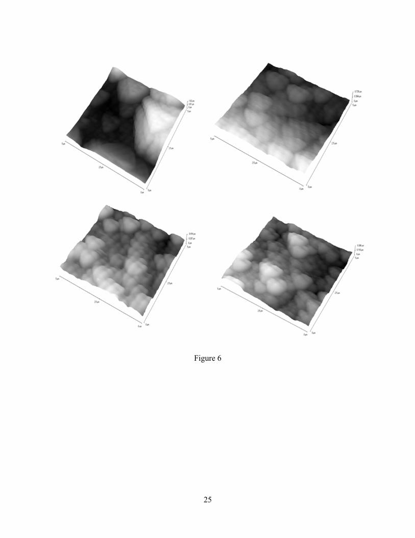
3D height mode topographical AFM image of large scan area, 5 × 5 µm2, for the sonicated
deposit is shown in fig. 6. The most heighted grains belong to the range of 1.62 µm. Average
grains have the height of 599 nm. The average roughness factor is 386 nm. Deposits at further
low temperature are closely spaced finer copper mushrooms. The grains at 15 ºC do fall in the
height range of 0-733 nm with the average roughness factor of 152 nm. Significant in appearance
can be observed at 10 °C. The micro domains have started engulfing their boundaries, which

12
may indicate the compactness of the films. Sonicated deposits are well covered than the silent
deposits confirming higher throwing power and current efficiency even at low temperature. The
non-uniform coalesced mushrooms at 10 °C are observed to have a greater degree of smoothness
at 5 ºC. Micro-polishing of the surfaces may result high coplanarity and smooth surface for use
in electronic industries. The AFM micrograph at 5 ºC is shown in fig. 6 (d). The grains have the
average height and roughness factor of 167 nm and 60 nm respectively. This result indicated the
highest surface finish of the deposit at 5 °C bath temperature, among all the deposits.
An exclusive explication on the frequently observed mushroom structures is still inadequate in
the open literature. And the explanation stems from the well established fact that electric charge
neutrality can be assumed, except within a thin boundary layer of exceptionally high electric
field (106 or 107 V/cm), at the surface of the cathode [24]. The electrodeposition processes,
uniform forward and backward diffusion of adsorbing depositing ions and desorbing byproducts
respectively, occur in this very thin region of metal-solution interphase. And the behavior of a
kinetically control system is to encompass a layer as thin as possible for the ease of the sequence
of processes. Ultrasound waves could indeed thin down the diffusion layer and reduces the
depletion of electroactive surface near the substrate [25], resulting in the formation of facets on
the existing nuclei.
A comparative compositional analysis from the EDS result has given in Table 2. The results
show that the sonicated deposits are cleaner as compared to the silent. The findings do support
the in-situ cleaning and the inconvenience for the undesired reactions as reported by the authors
for deposition onto graphite electrodes.

13
3.4 Thermal stability analysis
Figure 7 shows the heat absorption measurement data for the films. The scale is represented in
exothermic setting. It can be observed that the heat absorved with decreased temperature
increases from 2 to 8 mW. However, we have not calculated exactly the specific heat change
associated with the nano-garined deposits, but the change in lattice energy states in terms of
amount of heat absorbed with the size. Furthermore the film deposietd at 5 °C shows a tendency
of grain growth, as observed from small exothermic peaks in the thermogram. The above
observations can be explained by the fact that, the specific heat of a bulk solid was calculated by
Einstein in 1910 by assuming that all of the atoms have one and the same vibration frequency. In
1940, it was found that there is a soft-phonon mode, the frequency of which varies with
temperature, moving toward the Rayleigh line and reaching zero at the transition temperature so
that there is a contribution to the specific heat that vanishes at the transition temperature. Hence
phonon scattering generated at the grain boundaries of nanocrystals are well expected. This
scattering generates new phonon frequencies in a nanocrystal, which contributes to the specific
heat in terms of lattice energy. Thus, the size dependence of the lattice energy, E, is described by
equation 4 [26]:
T exp (4)
Where, b1 and α are constants, T is absolute temperature. Thus, there is a large change in lattice
energy for a small change in size, d , of the nanocrystal due to phonon scattering at the surface.
Hence, the reduction in grain size of the films with low deposition temperatures will consume

14
heat to accommodate the change in latticle energy. While ultrafine grains may also show a
tendency of grain growth (as in 5 °C film) due to to grain boundary motion.
3.5 Mechanical property
Figure 8 depicts the variations of thickness and mechanical properties of the films produced at
different deposition temperatures. The maximum load exerted on the films was 10 mN.
Thickness of films have been measured by the peak and valley method of AFM analysis. In the
nanoindentation technique hardness and Young’s modulus can be determined by the Oliver and
Pharr method [27], where hardness (H) can be defined as, , Pmax is maximum applied
load, Ac is contact area at maximum load. The ratio of maximum indentor depth to coating
tickness should be limited at 1/5, 1/10 and even 1/20 to eliminate the influence of substrate
deformation on measurement. The maximum displacement observed is 350 nm, 1/5 times of the
total thickness of the coating (1.7 µm). The reported hardness value of copper thin films is in the
range of 1-3 GPa [28], which are harder than the aluminium substrate (0.1-1 GPa). Hence the
coating hardness values may considered to be not affected by the substrate effects. It can be seen
that the displacement decreases with decreasing temperature. The hardness values observed are
in the range from 1.26 – 2.7 GPa. Copper films at temperatures below 15 ºC have hardness above
the hardness values for pure crystalline copper (1-1.5 GPa) [29]. This can be attributed both to
grain size strengthening (small grains compared to the grain size of pure crystalline copper)
and/or strain hardening. The grain size strengthening is determined by the strength of Cu grains
(H0) and the average grain size (d) of Cu according to the Hall-Petch relation ( 2/1−+= kdHH o ),
where k, Hall-Petch coefficient accounting the grain boundary resistance to dislocation

15
movement. Thus, the increased dislocation piled up with decreasing size has resulted in such
high strength films. The determined Young’s modulus values range from 92 -175 GPa.
Recently Leyland et. al. [30] have reported, that moderately soft materials can achieve high wear
resistance and ductility, if they pose high H/E ratio. The H/E values are greater than 0.01,
obtained for almost at all the temperatures and exceeds for pure crystalline copper (0.008) [31].
This suggests that fairly improved wear properties can be achieved for this inherently soft
material.
4. Conclusion
The effects of ultrasound and temperature for copper electrodeposition on aluminum were
studied using cyclic voltammetry and microscopy techniques. Silent deposition showed a mixed
kinetics control while sonicated system was dominantly charge transfer control. Films were
crystalline in structure. The deposits from the doubly activated bath have the distinct mushroom
like morphologies, while in silent conditions there was a transition of morphology from dendritic
structures to spherical grains with decrease in deposition temperature. Further, the addition of
sonication environment has lead to substantial variations of thermal and mechanical properties of
the copper thin films. There was a significant change in the variation of energy absorbed for
films that deposited at different bath temperatures. The observed hardness values of the films
were higher than the conventional polycrystalline copper. Further the soft films were found to
have good wear properties. Thus, the beneficial sonication effect on deposits may be effortlessly
and suitably tailored depending on the requirement, which holds a great promise for the future.

16
Acknowledgement:
The authors would like to thank the National Institute of Technology (NIT) for providing the
necessary financial and infrastructural supports.
References
[1] O. Kardos, D. G. Foulke, in: C. W. Tobais (Ed.): Advances in Electrochemistry and
Electrochemical Engineering, Interscience, New York (1962).
[2] M. Palomar-Pardave, N. Batina, I. Gonzalez, J. Phys. Chem. B 104 (2000) 3545.
[3] N. D. Nikolic, K. I. Popov, L. J. Pavolvic, M. G. Pavolvic, Surf. Coat. Technol. 201 (2006)
560.
[4] D. Grujicic, B.Pesic, Electrochim. Acta 47 (2002) 2901.
[5] M. A. Pasquale, L. M. Gassa, A. J. Arvia, Electrochim. Acta 53 (2008) 5891.
[6] E. Barrera, M. Palomar-Pardave, N. Batina, I. Gonzalez, J. Electrochem. Soc. 147 (2000)
1787.
[7] J. S. Santos, R. Matos, F. Trivinho-Strixino, E.C. Pereira, Electrochim. Acta 53 (2007) 644.
[8] A. Mallik, B. C. Ray, Thin Solid Films 517 (2009) 6612.
[9] A. Gedanken, Ultrason. Sonochem. 11 (2004) 47.
[10] J.P. Lorimer, T.J. Mason, Chem. Soc. Rev. 16 (1987) 239.
[11] A. Mallik, A. Bankoti, B. C. Ray, Electrochem. Solid-State Lett. 12 (2009) F46.
[12] T. J. Mason, J. P. Lorimer, D. M. Bates, Ultrasonics 31 (1992) 40.
[13] A. Mallik, B. C. Ray, Evolution of principle and practice of electrodeposited thin film: A
review on effect of temperature and sonication, International Journal of Electrochemistry (In
press).

17
[14] Chi-Chang Hu, Chi-Ming Wu, Surface and Coatings Technology 176 (2003) 75–83.
[15] Z. Zainal, A. Kassim, M. Z. Hussein, C. H. Ching, Materials Letters 58 (2004) 2199– 2202.
[16] N.D. Nikolić, K.I. Popov, Lj. J. Pavlović, M.G. Pavlović, Surface & Coatings Technology
201 (2006) 560–566.
[17] A. A. Rasmussen, J. A.D. Jensen, A. Horsewell, M. A.J. Somers, Electrochimica Acta 47
(2001) 67–74.
[18] G. K. Williamson, W. H. Hall, Acta Metall. 1 (1953) 22.
[19] M. A. Margulis, I. M. Margulis, Ultrason. Sonochem 10 (2003) 343.
[20] T. J. Mason, J. P. Lorimer, D. M. Bates, Ultrasonics 30 (1992) 40.
[21] C. Ramirez, E. M. Arce, M. Romero-Romo, M. Palomar-Pardave, Solid State Ionics 169
(2004) 81.
[22] B. D. Cullity, Elements of X-Ray Diffraction Addison-Wesley Publisher, MA (1978).
[23] International Centre for Diffraction Data (ICDD), Card No. 04-0863.
[24] M. Paunovic, M. Schlesinger, Fundamentals of Eelectrochemical Deposition, Wiley
Interscience, USA (2006).
[25] F. Marken, R. P. Akkermans, R. G. Compton, J. Electroanal. Chem. 145 (1996) 55.
[26] K. N. Srivastava, Nano Lett. 2 (2002) 21.
[27] W. C. Oliver, G. M. Pharr, J. Mater. Res. 7 (1992) 1562.
[28] D. Beegan, S. Chowdhury, M.T. Laugier, Surf. Coat. Technol. 201 (2007) 5804.
[29] http://en.wikipedia.org/wiki/Copper/04/09/2010
[30] A. Leyland, A. Matthews, Wear 246 (2000) 1.
[31] K. W. McElhaney, J. J. Vlassak, W. D. Nix, J. Mater. Res. 13 (1998) 1300.

18
Figure Captions Figure 1: (a) Change in solvent temperature under sonication as a function of time at various temperatures; (b) Ultrasonic power calculated at various temperatures Figure 2: Cyclic voltammetry for copper deposits at various temperatures (a) without sonication, (b) with sonication and (c) dependence of scan rate on current in silent condition at 20 °C
Figure 3: XRD patterns of copper thin films prepared at different temperatures (a) without sonication and (b) with sonication.
Figure 4: SEM micrographs of electrodeposied copper at (a) 20 °C, (b) 15 °C, (c) 10 °C and (d) 5 °C
Figure 5: SEM micrographs of sono-electrodeposied copper at (a) 20 °C, (b) 15 °C, (c) 10 °C and (d) 5 °C. Figure 6: AFM micrographs of sono-electrodeposied copper at (a) 20 °C, (b) 15 °C, (c) 10 °C and (d) 5 °C.
Figure 7: DSC curves of sono-electrodeposited copper thin films Figure 8: Variation of (a) hardness and thickness and (b) elasticity and H/E ratio values with deposition temperatures

19
Table 1: Stripping charge/Deposition charge (Qa/Qc) of sonicated and silent copper depositions
Temperature (°C) Stripping charge/Deposition charge (Qa/Qc) Silent Sonication
20 0.8 0.9 15 0.72 0.99 10 0.7 1.01 5 0.6 1.01
Table 2: EDS compositional analysis of silent and sonicated copper deposits
Temperature Silent Composition (at%) Sonication Composition (at%) Cu O S Cu O S
20 72 25.90 2.10 100 - - 15 65.05 33.72 1.23 100 - - 10 61.85 37.12 1.03 100 - - 5 54.5 45 0.5 100 - -

20
Figure 1

21
Figure 2

22
Figure 3

23
Figure 4

24
Figure 5
25
Figure 6

26
Figure 7

27
Figure 8