april 8, 2005mos-ak, strasbourg self-heating investigation of bulk and soi transistors pierre-yvan...
TRANSCRIPT

April 8, 2005 MOS-AK, Strasbourg
Self-heating investigation of bulk and SOI transistors
Pierre-Yvan Sulima, Hélène Beckrich, Jean Luc Battaglia, Thomas Zimmer
University of Bordeaux 1, France
ST Microelectronics

April 8, 2005 MOS-AK, Strasbourg 2/32
Preface
This presentation deals • with bipolar transistors
• with heat transfer
• but: Heat transfer is material dependant
• MOS & BJT => Si
• Results are valid for MOS, too ? So, this presentation may interest you

April 8, 2005 MOS-AK, Strasbourg 3/32
Outline
Introduction: self-heating Measurement set-up Self-heating modelling Equivalent networks Predictive model Results, conclusion and perspectives

April 8, 2005 MOS-AK, Strasbourg 4/32
Introduction: macroscopic
Self-heating: • Heating of the device due to its power
dissipation
Bipolar transistor:
• P = IC VCE + IB VBE
• T = P ZTH

April 8, 2005 MOS-AK, Strasbourg 5/32
Introduction: impact
Electrical Power T changes Temperature variation
• Mobility variation
• E-gap variation
• IC, IB variation
• Electrical power variation Feedback: convergence problems for
electrical and physical simulators Limit of operation in high power region

April 8, 2005 MOS-AK, Strasbourg 6/32
Measurement set-up: step 1
Bipolar transistor
Ib
T Vce
Oscillo.
0.0
0.5
1.0
1.5
2.0
2.5
-10 0 10 20 30 40 50
t (µs)
Vce
(V)
0.915
0.920
0.925
0.930
0.935
0.940
0.945
-5 0 5 10 15 20 25 30 35 40 45
t (µs)
Vb
e (V
)
VBE(t):
VCE(t):
April 8, 2005 MOS-AK, Strasbourg 7/32
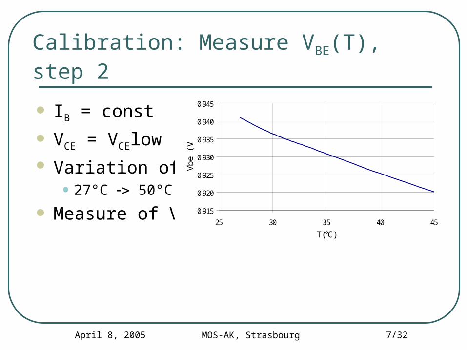
Calibration: Measure VBE(T), step 2
IB = const
VCE = VCElow Variation of T
• 27°C 50°C
Measure of VBE0.915
0.920
0.925
0.930
0.935
0.940
0.945
25 30 35 40 45
T(°C)
Vbe
(V
)

April 8, 2005 MOS-AK, Strasbourg 8/32
Dynamic behaviour: Trise(time)
From VBE(t) And VBE(T) Trise (t)
New method which permits to take into account the temperature rise @ VCE=VCEmin => Mixdes05
0
2
4
6
8
10
12
14
16
18
20
0 5 10 15 20Time (µs)
Tris
e (K
)

April 8, 2005 MOS-AK, Strasbourg 9/32
Electrical modelling of Trise(t)
State of the art(VBIC, MEXTRAM, HICUM)
Results
RTH CTH
Trise
B
C
E
Pdiss
0
1
2
3
4
5
0 2 4 6 8 10Time (µs)
Trise
(K)
measuresingle exponential modeldouble exponential model
THTH
THTH CpR
RpZ
1
t
TtTrise exp1

April 8, 2005 MOS-AK, Strasbourg 10/32
New thermal self-heating model
The differential equation describing heat transfer is:•
: thermal conductivity, [W/m°C]
• c: specific heat, [J/kg°C]: material density, [kg/m3]
• T: temperature, [°C] /c: thermal diffusivity, [m2/s]
t
TcT

April 8, 2005 MOS-AK, Strasbourg 11/32
Geometric presentation
0 L
x
y
z
W
heat source
q (r,t)
r
z
r0
Transistor, HBT
Schematic system representation with Cartesian co-ordinates
Schematic system representation with cylindrical co-ordinates: bidimensional axisymmetric geometry
t
T
az
T
r
T
rr
T
11
2
2
2
2
t
TcT
WL
r0

April 8, 2005 MOS-AK, Strasbourg 12/32
Boundary & initial conditions
q (r,t)
r
z
r0
Initial condition: t=0,
0,0
rforr
T
zrforTT ,,
00,0),( rrzfortrqz
T
0,00 rrzforz
T
TT

April 8, 2005 MOS-AK, Strasbourg 13/32
Analytical problem resolution
Calculation of the thermal impedance Trise(t) = Pdiss(t) ZTH(t) Transform into the Laplace domain and
solution of differential equation: pCR
R
RZ
pZTHTH
TH
THeq
TH
1111
)( q0Zeq
Rth
0

April 8, 2005 MOS-AK, Strasbourg 14/32
Comparison
Standard• Thermal impedance:
• Step response:
New model• Thermal impedance:
• Step response:
THTH
THTH CpR
RpZ
1
t
TtTrise exp1
B
terfc
B
texp1A)t(T
2rise
pCR
R
RZ
pZTHTH
TH
THeq
TH
1111
)(

April 8, 2005 MOS-AK, Strasbourg 15/32
Results (1)
Comparison between the standard (double exponential) and new model• a 1E2B2C 0.5x10 µm device
0
1
2
3
4
5
0 2 4 6 8 10
Time (µs)
Trise
(K)
measure
double exponential model
new model

April 8, 2005 MOS-AK, Strasbourg 16/32
Results (2)
0
2
4
6
8
10
12
14
16
18
20
0 5 10 15 20Time (µs)
Tri
se (
K)
measure
new model
IB = 150µA
IB = 50µA
Measurement for different Ib currents @ different power dissipation
• a 1E1B1C 0.8x6.4 µm device

April 8, 2005 MOS-AK, Strasbourg 17/32
Equivalent networks
Electrical-thermal networks for SPICE simulation
• Represent the thermal impedance as accurate as possible
• Have as few parameters as possible
• The parameters have a physical meaning
pCR
RpZ
THTH
THTH
1
)(

April 8, 2005 MOS-AK, Strasbourg 18/32
Equivalent network recursive parallel
Recursive parallel network
RTHPdiss
Tel
C
R
kC
kR
Ki-1C
Ki-1R
k2C
k2R
Ztrans

April 8, 2005 MOS-AK, Strasbourg 19/32
Results:recursive parallel
Recursive parallel network • N=10
• RTH, R, C, k
4 parameters have to be determined
Independent of cell number
1
10
100
1000
10000
1.0E+00 1.0E+02 1.0E+04 1.0E+06 1.0E+08 1.0E+10 1.0E+12
Frequency (Hz)
ZT
H (
K/W
)
Analytical model
Parallel recursive network
-50
-40
-30
-20
-10
0
1.0E+00 1.0E+02 1.0E+04 1.0E+06 1.0E+08 1.0E+10 1.0E+12
Frequency (Hz)
Phas
e (°
)
Analytical model
Parallel recursive netw ork
-10dB/dec
- 45°

April 8, 2005 MOS-AK, Strasbourg 20/32
Time domain
Step response of the parallel recursive circuit
0
2
4
6
8
10
12
0 10 20 30 40 50Times (µs)
Tel (
°C)
Parallel recursive network
Exponential model
Measurement

April 8, 2005 MOS-AK, Strasbourg 21/32
Predictive Modelling
Calculate the thermal impedance as a function of the layout data• Numerical approach
• Geometrical approach

April 8, 2005 MOS-AK, Strasbourg 22/32
Numerical approach
HBT cross section: 3 layers: • back end (Isolation and metallization)• Active layer (intrinsic transistor + deep trench isolation)• Substrate
Resolving the Heat transfer equation with the specific initial and corner conditions
p
p SiGe
Burried layer n+
SiO2 SiO2SiO2
n+p+ p+
SIC n
BE
C
B
Substrate pp+ deep trench
Emitterpoly n+
Extrinsic basepoly p+
n épitaxial
SEG SiGe Base
Collector sinkern+
+
y
x
z
e0
e1
e2
Ф
λ2 (ρC)2
λ1
λ0
(ρC)1
(ρC)0
λe2Ф(t)
(ρC)e2
λe0
(ρC)e0
e2
z
(ρC)e1 λe1
x

April 8, 2005 MOS-AK, Strasbourg 23/32
Results (RTH = f(emitter area))
Physical approach Numerical calculation takes some minutes Actually: some problems with CTH scaling
RTH=f(Se)
0.00E+00
1.00E+03
2.00E+03
3.00E+03
4.00E+03
5.00E+03
6.00E+03
7.00E+03
0.00E+00 2.00E+00 4.00E+00 6.00E+00 8.00E+00
Se(µm2)
RT
H(K
/W) RTHIXLexp
RTHIXLexp2
RTHIXLnum
RTHST

April 8, 2005 MOS-AK, Strasbourg 24/32
Geometrical approach

April 8, 2005 MOS-AK, Strasbourg 25/32
RTH calculation

April 8, 2005 MOS-AK, Strasbourg 26/32
Results: output characteristics

April 8, 2005 MOS-AK, Strasbourg 27/32
HBT on SOI
Schematic Cross section TEM Cross section view
April 8, 2005 MOS-AK, Strasbourg 28/32
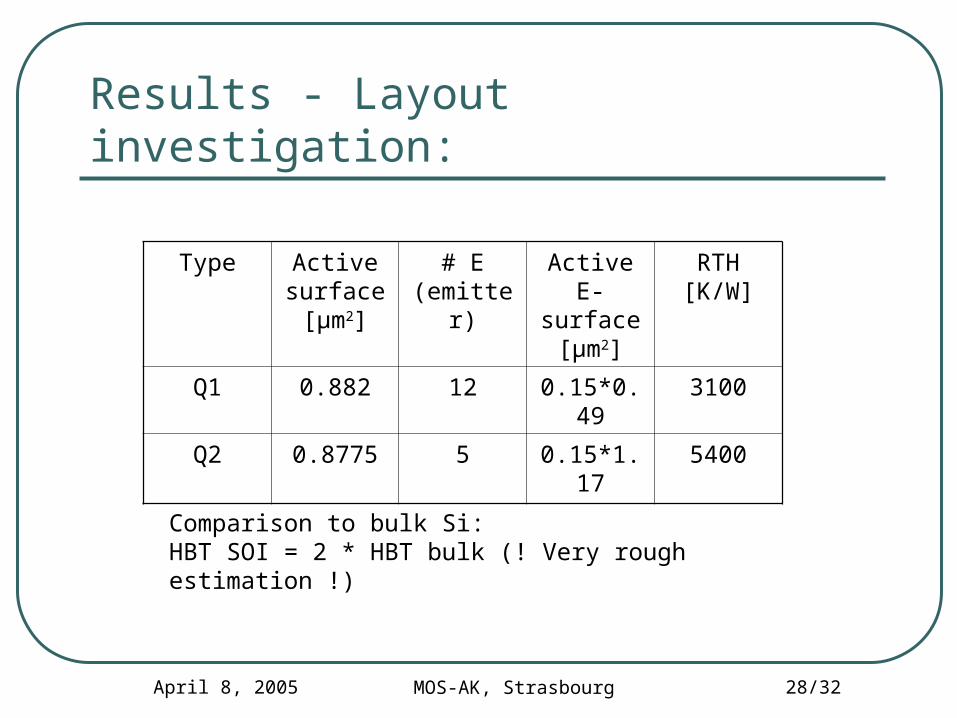
Results - Layout investigation:
Type Active surface [µm2]
# E(emitter)
Active E-surface [µm2]
RTH [K/W]
Q1 0.882 12 0.15*0.49 3100
Q2 0.8775 5 0.15*1.17 5400
Comparison to bulk Si: HBT SOI = 2 * HBT bulk (! Very rough estimation !)

April 8, 2005 MOS-AK, Strasbourg 29/32
Discussion Limit of the standard model Development of a new accurate model
• Resolution of heat transfer differential equation
• Physical model
Representation with equivalent networks • The parallel recursive network is very accurate
• 4 parameters needed
Use in compact circuit modelling

April 8, 2005 MOS-AK, Strasbourg 30/32
Under work: predictive model
Numerical approach Geometrical approach Both approaches give good results
• Calculation time
• Usability
Methods applied to HBT on SOI
April 8, 2005 MOS-AK, Strasbourg 31/32
Perspectives
Thermal coupling between transistors Power device modelling Layout optimisation Investigation of the thermal behaviour of MOS
transistors ? (cooperation)• Tools
• Methods
• Equations
• Extraction methods

April 8, 2005 MOS-AK, Strasbourg
Thanks for your attention
The paper is open for discussion.