applications of power electronics for renewable energy
TRANSCRIPT

University of Calgary
PRISM: University of Calgary's Digital Repository
Graduate Studies The Vault: Electronic Theses and Dissertations
2015-09-29
Applications of Power Electronics for Renewable
Energy
Mohamadiniaye Roodsari, Babak
Mohamadiniaye Roodsari, B. (2015). Applications of Power Electronics for Renewable Energy
(Unpublished doctoral thesis). University of Calgary, Calgary, AB. doi:10.11575/PRISM/24972
http://hdl.handle.net/11023/2538
doctoral thesis
University of Calgary graduate students retain copyright ownership and moral rights for their
thesis. You may use this material in any way that is permitted by the Copyright Act or through
licensing that has been assigned to the document. For uses that are not allowable under
copyright legislation or licensing, you are required to seek permission.
Downloaded from PRISM: https://prism.ucalgary.ca

UNIVERSITY OF CALGARY
Applications of Power Electronics for Renewable Energy
By
Babak Mohamadiniaye Roodsari
A THESIS
SUBMITTED TO THE FACULTY OF GRADUATE STUDIES
IN PARTIAL FULFILMENT OF THE REQUIREMENTS FOR THE
DEGREE OF DOCTOR OF PHILOSOPHY
GRADUATE PROGRAM IN ELECTRICAL AND COMPUTER ENGINEERING
CALGARY, ALBERTA
SEPTEMBER 2015
© Babak Mohamadiniaye Roodsari 2015

ii
Abstract
The use of renewable energy sources is growing in popularity despite the world’s present
dependence on fossil fuel energy. This growth is driven in part by technological improvements.
One form of renewable energy, hydro power, in recent decades has found a role in small scale
systems for rural villages, especially in the developing world. For such microhydro systems, it is
possible to control the loading on the generator by electronic means. However, the switching
nature of the power electronics introduces undesired harmonics and causes stress in the
generator. Hence, a new electronic load controller topology is proposed to reduce the level of the
injected harmonic content in the generator stator windings. Another issue in microhydro systems
is the lack of effective generator utilization where the generator is off for much of the day or
power is wasted in a dump load. Hence a novel controller is proposed, the distributed electronic
load controller, installed in each household to reduce the wasted energy in the powerhouse. In a
different context, solar photovoltaic power usually requires an inverter to produce AC electrical
power. However, there are several challenges in the design of inverter control for photovoltaic
and other applications. Modern space vector control methods while providing more flexibility as
compared to carrier based methods, have become complex in their implementation. A
computationally efficient, universal fast Space Vector Modulation (SVM) algorithm is proposed
for the multilevel inverter. The multilevel inverter topology is becoming increasingly popular for
many industry applications, but has great appeal in photovoltaic systems since multiple DC
sources can be taken advantage of. However, one drawback of multilevel inverter topologies is
the large number of switching devices. This increases the probability of failure and decreases
system reliability. The high execution speed and simplicity of the proposed fast SVM method is
refined and extended in the case of fault tolerant systems and in the case of imbalanced input

iii
voltage and power. Simulation and experimental verifications indicate that the proposed
electronic load control concepts and SVM concepts are valuable for further investigations.

iv
Acknowledgement
I would like to express my sincere thanks to my supervisor, Dr. Edwin Peter Nowicki, for his
outstanding efforts, constant support, advice, patience, encouragement and most importantly his
friendship throughout my study at the University of Calgary. I have learned from his brilliant
personality a lot, not only in research work, but also in life.
I greatly appreciate the advice, assistance, inspiration and support received from my co-
supervisor Dr. David Howe Wood from the Mechanical and Manufacturing Engineering
Department. His continuous flow of inventive ideas inspired me to try new ideas. He very
modestly did not wish to be a co-author of papers but still took the time to perform careful
reviews of the papers related to the dissertation.
I also wish to thank my thesis committee members, including the candidacy committee
members: Dr. C. J. B. Macnab, Mr. N. Bartley, Dr. L. Behjat, Dr. S. Mehta, Dr. Q. K. Hassan,
and Dr. M. N. Uddin for their guidance, ideas and feedback.
I am deeply grateful to graduate administrators and electrical technologists in the Department
of Electrical and Computer Engineering. Thank you, Ella Lok, Anna Grykalowska, Jinny Kim,
Lisa Besmiller, Ivana D’Adamo, Garwin Hancock, and Rob Thomson. I also would especially
like to thank Richard Galambos for his support and endurance to prepare the project prototype.
I would like to thank my amazing family for the encouragement I have obtained over the years.
In particular, my deepest gratitude, appreciation and admiration go to my dear wife, Fatima and
my wonderful daughter, Tina, for their unfailing love, support, and patience. I undoubtedly could
not have done this without you.

v
Dedication
To My Family

vi
Table of Contents
Abstract………………………………………………………………………...…………………iii
Acknowledgements …………………………………………………………………..…………...v
Dedication………………………..…………………………………………………………...…..vi
Table of Contents………………………………………………………………………………...vii
List of Tables………………………………………………….……………………….……....…xi
List of Figures…………………………...……………………………………………….….…...xii
List of Principal Symbols…………………………………………………………………..….....xx
List of Abbreviations…………………………………………………………………………...xxv
Chapter One: INTRODUCTION
1.1 Background……………………………………………………………………....……………1
1.2 Microhydro Systems…………………………………………………………………….....….1
1.2.1 The need for microhydro……………………………………………….…………….1
1.2.2 Induction generators and electronic load control………………………...…………..2
1.3 Multilevel Inverter Topologies and Control…………………………………………..………3
1.3.1 Space vector modulation methods……………………………...…………………….5
1.3.2 Power balance control of photovoltaic systems……………...……………………….6
1.3.3 Fault tolerant modulation methods………………………………..……………...…..7
1.4 Motivations Underlying the Proposed Research………………………………………………7
1.5 Thesis Outline……………………………………………………………………………..…10
1.6 List of Publications (some in preparation) Related to Dissertation Work……………..…….13
Chapter Two: A NEW ELECTRONIC LOAD CONTROLLER FOR THE SELF-EXCITED
INDUCTION GENERATOR TO DECREASE STATOR WINDING STRESS
2.1 Introduction…………………………………………………………………………………..15
2.2 Induction Generator and System Modeling………………………………………………….19

vii
2.3 Proposed Electronic Load Controller………………………………………………….…….21
2.3.1 Proposed ELC topology………………….………………………………………….21
2.3.2 Design Procedure of the Proposed ELC…………………...………………………..24
2.4 Simulation Results……………………………………………………………………….…..27
2.5 Chapter Summery…………………………………….………………………………...……33
Chapter Three: THE DISTRIBUTED ELECTRONIC LOAD CONTROLLER: A NEW
CONCEPT FOR VOLTAGE REGULATION IN MICROHYDRO SYSTEMS WITH
TRANSFER OF EXCESS POWER TO HOUSEHOLDS
3.1 Introduction………………………………………………………………………….……….34
3.2 System Modeling……………………………………………………………………….……39
3.3 Proposed Distributed Electronic Load Controller……………………………………………40
3.4 Simulation Results………………………………………………………………………...…45
3.5 Chapter Summery ……………………….…………………………………………………..53
Chapter Four: ANALYSIS AND EXPERIMENTAL INVESTIGATION OF THE IMPROVED
4.1 Introduction ……………………………………………………………………………...…..55
4.2 The Improved DELC Configuration and Benefits………………………………...…………58
4.3 The design considerations for the proposed system…………………………………...…….60
4.3.1 Principles of the proposed AC chopper…………..………………………….….…..60
4.3.2 Improved DELC dump load sizing consideration….……………………….……….63
4.3.3 Improved DELC input filter design……………………………………….……...…63
4.3.4 ELC dump load selection consideration………………………………………...…..68
4.4 Experimental and Simulation Results………………………………………………………..69
4.4.1 Experimental and simulation results for the proposed improved DELC system…....69
4.4.2 Simulation study: interconnection between the proposed improved DELC
units and the ELC units……………...……..………......…………..…………..…....73
4.5 Chapter Summery …………………….……………………………………………………..76

viii
Chapter Five: AN EFFICIENT AND UNIVERSAL SPACE VECTOR MODULATION
ALGORITHM FOR A GENERAL MULTILEVEL INVERTER
5.1 Introduction…………………………………………………………………………………..78
5.2 Background of the SVM Approach…………………………………...……………………..81
5.3 Proposed Complementary SVM Method……………………………………………….……82
5.3.1 Utilized definitions……………………………………...……….…………………..82
5.3.2 Problem formulization…………………………………………….……..………….83
5.3.3 Switch on-time duration…………………………………………….…….…………86
5.3.4 Switch states ……………………………………………………….…………….….92
5.3.5 The proposed flowchart used in programming of a digital signal processor………..93
5.4 Simulation and Experimental Results………………………………………………………..97
5.5 Chapter Summery ………………………….……………………………………………....102
Chapter Six: A FAST AND UNIVERSAL FAULT TOLERANT SPACE VECTOR
MODULATION METHODS FOR THE MULTILEVEL CASCADED H-BRIDGE INVERTER
6.1 Introduction…………………………………………………………………………..…………….103
6.2 Proposed Virtual Voltage Concept……………………………..……………………………….105
6.3 Proposed Virtual SVM Method………………………………..………………………………..108
6.3.1 Proposed switching sequences………………………………………..………………..109
6.3.2 Proposed mean switching states………………………………..………………………110
6.3.3 Proposed virtual SVM method………………………...…………………………..116
6.3.4 Proposed method to find the switching states…………………….………………..118
6.3.5 Calculation of maximum modulation index……………………......………………120
6.4 Simulation and Experimental Results…………………………………………...………….121
6.6 Chapter Summery ………………………………………………………………….………126

ix
Chapter Seven: A DYNAMIC SPACE VECTOR MODULATION METHOD FOR POWER
BALANCE CONTROL OF PHOTOVOLTAIC SYSTEMS
7.1 Introduction…………………………………………………………….……....……….….127
7.2 Outline of the Proposed Approaches……………………………………….….……….….129
7.2.1 Proposed power sharing method………………………………………....…….….130
7.2.2 Proposed effective switching states concept……………… ……..…….….……..133
7.2.3 Proposed dynamic SVM method……………………………...……….….……….139
7.2.3.1 Switch on-time duration calculation…………………......……….…….……...139
7.2.3.2 Proposed method for finding switching states…………...…...….….……...….143
7.2.4 Proposed formula for the maximum modulation index………….………...…..…..143
7.3 Simulation and Experimental Results………………………………….……….……..……145
7.5 Chapter Summery ……………………………………………………………….………....149
Chapter Eight: CONCLUSION AND FUTURE WORK
8.1 Conclusions ………………………………………………………………………………...151
8.2 Recommendations for Future Work ………………………..………………………………152
REFERENCES…………………………………………………………………………………155
Appendix A: DISTRIBUTED ELECTRONIC LOAD CONTROLLER:
OPERATION, CALIBRATION, AND TROUBLESHOOTING
A.1 Introduction………………………………………………………………………………...175
A.2 DC Power Supplies………………………………………………………………………...176
A.3 Current Sensor……………………………………………………………………………...178
A.3.1 Calibration method………………………………………………………………..179
A.4 Microcontroller…………………………………………………………………………….182
A.4.1 Test method……………………………………………………………………….183
A.5 IGBT Drive Circuit………………………………………………………………………...186
A.5.1 Test method……………………………………………………….……………….186

x
A.6 Digital Thermocouple………………………………………………………...……………188
A.6.1 Instructions for controlling the temperature………………….…………………...189
A.7 Bi-Directional IGBT Switches……………………………………………………………..191
A.7.1 Bi-directional IGBT switches test………………………….……………………...193
A.8 Water Heater Element…………………………………………………………………..….194
Appendix B: EXPERIMENTAL INVESTIGATIONS OF THE DELC
B.1 Shematic Digrams.................................................................................................................198
B.2 Field Investigation in Nepal..................................................................................................199
B.2 Experimental Investigation in the Power Electronic Research Laboratory………….…….199
Appendix C: EXPERIMENTAL SET-UP FOR MULTILEVEL INVERTER
C.1 𝑒𝑍𝑑𝑠𝑝𝑇𝑀F2812.....................................................................................................................203
C.2 IRG4BC20UD.......................................................................................................................206
C.3 FOD3184...............................................................................................................................207
C. 3. 1 Block diagram of the gate drive circuit..................................................................207
C.4 Experimental Investigation in the Power Electronics Research Laboratory……………….207
C.5 Detail Formulation of Chapter Five..………………………………………………………209

xi
List of Tables
Table 2.1 The considered consumer load pattern with two step changes at
5.5 seconds and 8.5 seconds
28
Table 3.1 The considered households’ loads pattern with two step changes
in 5 and 8.5 seconds
47
Table 4.1 Considered consumer (household) load conditions 75
Table 5.1 The on-time duration calculation details based on proposed
complementary SVM method
93
Table 5.2 A comparison of SVM execution time (1 per unit time
corresponds to 𝟏𝟓. 𝟑µ𝐬𝐞𝐜 a TMS320F2812)
101
Table 6.1 Typical voltage level redundancies in a 7-level CHB inverter topology 109
Table 6.2 Effect of virtual voltage on space vector coordinates 112
Table 6.3 Three main sub-triangles coordinates and their related angular spacing 120
Table 6.4 Examples of detailed calculation for the proposed virtual SVM
approach
120
Table 7.1 Voltage level redundancies for a 3-phase 5-level CHB inverter (phase
A)
132
Table 7.2 DC voltages, MMI and total power for considered CHB in simulation 146
Table A.1 DIP switch arrangements with respect to heater rating and allocated
power to a given household
185
Table A.2 a summarized of failures in bi-directional IGBT unit 195
Table C.1 𝑒𝑍𝑑𝑠𝑝𝑇𝑀F2812 Connectors 204
Table C.2 Main features of the 𝑒𝑍𝑑𝑠𝑝𝑇𝑀F2812 205
Table C.3 Main features of TMS320F2812 DSP 205

xii
List of Figures
Figure2.1 Dynamic or d-q equivalent circuit of an induction generator (in
stationery reference frame ωe is equal to zero)
20
Figure 2.2 The Simulink block employed for the designed induction generator 22
Figure 2.3 a) SEIG, excitation capacitor bank and ELC blocks and associated gate
control circuit blocks, b) the proposed ELC topology, and c) utilized
topology in [11]
22
Figure 2.4 Equivalent loads seen by ELC terminals, proposed ELC when 𝑺𝒋 is a)
open, b) closed, conventional ELC topology when 𝑺𝒋 is c) open, d)
closed, and e) associated generator terminal resistance based on
aforementioned topologies
23
Figure 2.5 Typical system characteristics, a) magnetizing inductance, b)
magnetizing current, c) RMS output voltage (dashed line: no ELC;
black line: with proposed ELC) , d) output power with (gray) and
without ELC (black), and e) instantaneous output voltage with
proposed ELC
29
Figure 2.6 Instantaneous total customer current of the unbalanced 3-phase load 29
Figure 2.7 The instantaneous current of the ELC for each phase 30
Figure 2.8 The average output power for each phase including, load power, ELC
power and total power
31
Figure 2.9 The dump load instantaneous currents, a), b), c), and d) proposed
topology with load resistance equal to 55, 95, 150, and 300Ω,
respectively; e), f), g), and h) are corresponding waveforms for the
topology in [11] with the same consumer loads
31
Figure 2.10 The stator current harmonic content: a), b), c) and d) for proposed
topology with load resistance equal to 55, 95, 150, and 300Ω,
respectively; e), f), g) and h) are corresponding waveforms for the
topology in [11] with the same consumer loads
32
Figure 2.11 The THD level with respect to per-phase load current, a) for stator

xiii
current, b) for output voltage 32
Figure 3.1 a) DELC configuration, including SEIG, capacitor bank, and low rated
ELC, n separated DELC per-phase and b) related gate control blocks
42
Figure 3.2 Equivalent circuit of the proposed DELC 43
Figure 3.3 A simple block diagram of the utilized control strategy in the proposed
DELC
43
Figure 3.4 Utilized control strategy for the low rated ELC 44
Figure 3.5 Typical system characteristics, a) magnetizing inductance, b)
magnetizing current, c) instantaneous output voltage, d) RMS output
voltage, e) considered load current for a typical house hold in phase
“a”, f) the DELC chopped current, and g) the system frequency
47
Figure 3.6 System current consumption, a) to e) current consumption if all
households are connected to phase “a” based on selected load pattern
in Table 3.1, including regular load current with light gray shaded,
DELC current with dark gray shaded and the total current with block
color, f) current consumption in the phase “a” including the households
total consumption, shaded with light gray, the ELC current, shown
with dark gray, and total current for phase “a” with block shaded
48
Figure 3.7 The output voltage of phase “a” based on different failure scenarios
which may happen in system, a) no-load output voltage, b) output
voltage in the case of failure for all IGBT switches, c) output voltage in
the case of failure for all IGBT switches installed in DELCs, d) output
voltage in the case of failure among 2 IGBT switches installed for 5
households and failure in the ELC switch, e) output voltage in the case
of failure among 2 IGBT switches installed for 5 households, f) output
voltage in the case of failure in one household IGBT switch, g) output
voltage in the case of failure in installed IGBT switch for the
ELC, and h) output voltage without failure
51
Figure 3.8 The total output power of induction generator based on different failure

xiv
scenarios which maybe happen in system, a) no-load output power, b)
output power in the case of failure for all IGBT switches, c) output
power in the case of failure for all IGBT switches installed in DELCs,
d) output power in the case of failure among 2 IGBT switches installed
for 5 households and failure in the ELC switch, e) output power in the
case of failure among 2 IGBT switches installed for 5 households, f)
output power in the case of failure in one household IGBT switch, g)
output power in the case of failure in installed IGBT switch for the
ELC, and h) output power without failure
52
Figure 3.9 Output voltage and power in the case of sinusoidal distortion in water
flow rate, a) output power for system with low rated ELC, b) output
power for system without low rated ELC, c) output voltage for system
with low rated ELC, and d) output voltage for system without low
rated ELC
53
Figure 4.1 a) System organization of powerhouse ELC and improved DELC units
in households, and b) general AC chopper circuit for ELC and DELC
61
Figure 4.2 Power transferred to the dump load as a function of PWM duty-ratio
for a) allocated power = dump load power rating and b) allocated
power = 0.33 dump load power rating
63
Figure 4.3 a) Proposed improved DELC circuit b) and c) equivalent circuit for
calculating the effect of switching disturbance in input current, d)
equivalent circuit for calculating of the displacement factor
66
Figure 4.4 Photographs of prototype improved DELC unit 71
Figure 4.5 Control strategy for a) the improved DELC, and b) the ELC units 71
Figure 4.6 Experimental investigation a) PWM waveform, b) DELC dump load
voltage, and c) input source current without filter
72
Figure 4.7 Input source current of the improved DELC unit a) experimental
results, and b) simulation results
72
Figure 4.8 Important specifications of the improved DELC a) total active power,

xv
b) reactive power, c) power factor, and d) THD level 72
Figure 4.9 Network characteristics a) consumer regular load currents, b) the
DELC dump load current, and c) instantaneous voltage
75
Figure 4.10 Current consumption, THD level and power factor for a particular
phase (phase “a”) of the system, a1) to e1) current consumption for
consumers and the improved DELC units, f1) total consumer current
and ELC current, a2) to e2) consumer THD level and power factor, f2)
THD level and power factor for phase “a”
76
Figure 4.11 Voltage variation with respect to different fault scenario 76
Figure 5.1 SVD for a 3-phase 7-level inverter a) related state space voltages
which has been defined by three digit number , b) number of redundant
space voltages with respect to the figure legend, c) and d) positive and
negative main STs identification
85
Figure 5.2 SVD for a 3-phase 7-level inverter a) the voltage vector coordinates in
g-h plane (two digit number), and b) the introduced numbering format
(𝑷𝒌𝒍 for positive reference STs and 𝑵𝒌𝒍 for negative reference STs)
86
Figure 5.3 Illustration of perpendicular lines from the reference voltage to the
positive main ST, the negative main ST, the reference STs sides and
the mathematical relation between the illustrated perpendicular lines
and their floor parts, where (a) to (d) are correct conditions and (e) to
(h) are incorrect conditions
91
Figure 5.4 The flowchart for programming based on proposed complementary
SVM method
95
Figure 5.5 Simulation results for the 3-phase 7-level CHB inverter based on the
proposed complementary SVM method a) inverter line-to-neutral
voltages b) inverter line-to-line voltages, c) generated power by DC
sources, and d) generated 3-phase output currents and the output
voltage waveform spectra before filtering
98
Figure 5.6 Experimental results for the 3-phase 3-level CHB inverter based on the

xvi
proposed complementary SVM method a) inverter line-to-neutral
voltages b) inverter line-to-line voltages, c) generated power by DC
sources, and d) 3-phase output currents and the output voltage
waveform spectra before filtering
100
Figure 5.7 Experimental results for the 3-phase 5-level CHB inverter based on the
proposed complementary SVM method a) inverter line-to-neutral
voltages b) inverter line-to-line voltages, c) generated power by DC
sources, and d) 3-phase output currents and the output voltage
waveform spectra before filtering
101
Figure 6.1 Switch positions for one phase of 7-level CHB inverter topology 107
Figure 6.2 Effect of appropriate utilization of the voltage level redundancies on
output power, a) proper utilization of redundancies to maximize power,
and b) minimum switching variations
109
Figure 6.3 SVD for a 3-phase 7-level CHB inverter topology 112
Figure 6.4 Comparison between the healthy SVD and widely distributed voltage
vectors for faulty system
113
Figure 6.5 g-h plane and mean switching states for a 3-phase 7-level CHB inverter 115
Figure 6.6 Comparison between the SVD for the conventional fault tolerant SVM
method and proposed virtual SVD for different faulty conditions a)
healthy condition, b) 1 fault in phase “a”, c) 3 faults in phase “a”, and
d) case 1
116
Figure 6.7 a) Virtual SVD and proposed sub-triangle positions, b) illustration of
maximum modulation index definition
119
Figure 6.8 Simulation results for a 3-phase 7-level CHB inverter, a) phase
voltages with respect to inverter neutral point, b) line-to-line voltages,
c) 3-phase sinusoidal output voltages, and d) to f) injected power by
each of the DC sources
122
Figure 6.9 Experimental results for a 3-phase 5-level CHB inverter in healthy
condition, a) phase voltages, b) line-to-line voltages, c) injected power
by DC sources , and d) 3-phase sinusoidal output voltages
124

xvii
Figure 6.10 Experimental results for a 3-phase 5-level CHB inverter with one
faulty cell in phase “c” a) phase voltages, b) line-to-line voltages and c)
3-phase sinusoidal output voltages
124
Figure 6.11 Experimental results for a 3-phase 3-level CHB inverter with two
faulty cells in phase “c”, a) phase voltages, b) line-to-line voltages, and
c) 3-phase sinusoidal output voltages
125
Figure 6.12 Experimental results for a 3-phase 5-level CHB inverter with two
faulty cells in phase “c” and one faulty cell in phase “b”, a) phase
voltages, b) line-to-line voltages and, c) 3-phase sinusoidal output
voltages
125
Figure 7.1 Typical 3-phase n-level CHB inverter topology 132
Figure 7.2 a) Regular SVD for a typical 3-phase 5-level CHB inverter topology
with equal DC sources, b) and c) voltage space vectors for two
abnormal cases
136
Figure 7.3 Switching sequences for a typical reference sub-triangle 136
Figure 7.4 Effective SVD for different average DC source voltages, a) Normal
condition, b) The average voltage of selected DC sources are Vdca =
1, Vdcb = 0.9 and Vdcc = 0.8, c) The average voltage of selected DC
sources are Vdca = 1, Vdcb = 0.7 and Vdcc = 0.8 Effective SVD (black
shade) is illustrated superimposed over the regular SVD (gray shade)
in part b and c
138
Figure 7.5 Decomposed effective SVD and dynamic main sub-triangles
coordinates
141
Figure 7.6 Simulation results for 3-phase 7-level CHB inverter, a) inverter
output line-to-line voltage based on dynamic SVM method, b) inverter
line-to-line voltage based on conventional SVM, c) generated 3-phase
sinusoidal waveform based on proposed dynamic SVM method and
conventional SVM method, d) phase voltage after filtering and injected
min-max sequence, e) generated output power for each DC sources
based on proposed idea, and f) generated power for each DC sources

xviii
based on conventional SVM strategy 146
Figure 7.7 Experimental results for 3-phase 5-level CHB inverter, a) inverter
output line-to-line voltage based on dynamic SVM method, b) inverter
line-to-line voltage based on conventional SVM, c) generated 3-phase
sinusoidal waveform based on proposed dynamic SVM method and
conventional SVM method, d) phase voltage after filtering and injected
min-max sequence, e) generated output power for each DC sources
based on proposed dynamic SVM method, and f) generated power
based on conventional SVM strategy
148
Figure A.1 Block diagram of the proposed home electrical system 177
Figure A.2 Block diagram of the DELC 177
Figure A.3 DC power supplies (5V and 15V) 177
Figure A.4 Current sensor and Op-Amp circuit (Important note: G-5V is the
ground reference of the 5V DC supply).
180
Figure A.5 The test point TP3 waveform 181
Figure A.6 The expected test point TP4 waveform 181
Figure A.7 Distorted waveform, measured from TP4 which is not desirable 181
Figure A.8 The test point TP5 expected waveform 181
Figure A.9 The MSP430 microcontroller circuit board and its test points and
jumpers and 5pin dip switch
184
Figure A.10 PWM output wave form of the microcontroller with respect to non-
water-heater household power
185
Figure A.11 The IGBT drive circuit and its test points 191
Figure A.12 Wiring diagram of the WH7016G digital thermocouple unit 189
Figure A.13 Front view of the digital thermocouple unit and NTC sensor 190
Figure A.14 Bi-directional IGBT switches configuration and its related test point 194
Figure A.15 The bi-directional IGBT unit test result with respect to consumed
power by regular loads
195
Figure A.16 The bi-directional IGBT unit test result during different type of failures 196

xix
Figure A.17 DELC box terminal block (as viewed from outside the box). G-5 is
optional earth ground connection.
196
Figure A.18 DELC and household electrical system configuration 197
Figure B.1 Schematic diagram for the DELC AC chopper 199
Figure B.2 Schematic diagram for the DELC power supply 199
Figure B.3 Some typical pictures from our trip to Nepal 200
Figure B.4 250W micro hydro generation unit and dump load 200
Figure B.5 DELC Field tests in Nepal 201
Figure B.6 DELC experimental tests in the Power Electronics Laboratory 202
Figure C.1 Block diagram of the experimental set-up 203
Figure C.2 The 𝑒𝑍𝑑𝑠𝑝𝑇𝑀F2812 layout and its connectors 204
Figure C.3 IRG4BC20UD package 206
Figure C.4 Typical FOD3184 gate drive circuit 208
Figure C.5 Experimental set-ups for CHB multilevel inverters 208

xx
List of Principal Symbols
ωr Electrical rotor speed
ids Stator Direct Current
iqs Stator Quadrature Current
idr Rotor Direct Current
iqr Rotor Quadrature Current
idL Load Direct Current
iqL Load Quadrature Current
Vds Stator Direct Voltage
Vqs Stator Quadrature Voltage
Vdr Rotor Direct Voltage
Vqr Rotor Quadrature Voltage
VdL Load Direct Voltage
VqL Load Quadrature Voltage
Rs Stator resistance
Rr Rotor resistance
Ls Stator self inductance
Lr Rotor self inductance
Lm Mutual inductance between stator and rotor
im Magnetizing current in the d-q model
𝑇𝑒 Developed electromagnetic torque
𝑃 Number of generator poles
𝑇𝑠ℎ𝑎𝑓𝑡 Shaft torque
𝐽 Moment of inertia
𝑅𝐿𝑗(𝑡) Estimated total consumer loads
𝑉𝑗(𝑡) Consumer phase voltage
𝑖𝑅𝐿𝑗(𝑡) Consumer phase current
𝑅𝐿𝑚𝑖𝑛 Resistance, corresponding to the maximum consumer load

xxi
𝑅𝑑𝑗1 First portion of the dump load
𝑅𝑑𝑗2 Second portion of the dump
𝑅𝑜𝑓𝑓−𝐼𝐺𝐵𝑇 IGBT switch off resistances
𝑅𝑜𝑛−𝐼𝐺𝐵𝑇 IGBT switch on resistances
𝑅𝑑𝑗𝑎𝑣2(𝑡) Average calculated resistance as seen by chopper terminals
𝑇𝑐 Selected period for the PWM sawtooth waveform
𝑇𝑐−𝑜𝑓𝑓 Chopper off-time duration
𝑇𝑐−𝑜𝑛 Chopper on-time duration are selected period for the PWM sawtooth
waveform, chopper
𝑅𝑑𝑗𝑎𝑣(𝑡) Total dump load resistance seen by the ELC terminals
𝐼ℎℎ−𝑚𝑎𝑥 Maximum current for each household
𝑅ℎℎ−𝑚𝑖𝑛 Minimum load resistance for each household
𝑉𝑟𝑒𝑓𝑓 Output reference voltage
𝑃𝐼(𝑛) Sampled calculated input current for PWM
𝑅𝑟𝑒(𝑡) Instantaneous load for a typical household
𝑅𝑠𝑝(𝑡) Instantaneous special load which should be controlled by the DELC
𝐼𝑟𝑒(𝑡) Instantaneous regular consumed current for a typical household
𝑇𝑐 Considered time interval (period) for PWM signal
𝑇𝑜𝑛−ℎℎ(𝑡) Instantaneous on-time duration for bidirectional IGBT switch
𝑉𝑗−𝑒𝑟(𝑛) 𝑛𝑡ℎ measured RMS error voltage for phase “j”
𝑉𝑗−𝑜𝑢𝑡(𝑛) 𝑛𝑡ℎ sampled measured RMS output voltage for phase “j”
𝑔𝑗𝑠 Output waveform of the PWM generator
M Mass of water
∆𝐸 Heated energy given to the water
C Specific heat capacity of water
∆𝑇 Change in temperature of the
𝐹𝑋𝜑−𝑖(𝑡) Rectangular waveform (to model the chopper performance) for 𝑖𝑡ℎ selected
consumer

xxii
𝐷𝑋𝜑−𝑖(𝑡) Calculated on-time duration(to model the chopper performance) for 𝑖𝑡ℎ
selected consumer
𝑉𝑋𝜑−𝑖(𝑡) Chopper output voltage
𝑉𝑋𝜑−𝑖𝑓 Fundamental component of the chopper voltage
𝑉𝑋𝜑−𝑖ℎ Harmonic contents of the chopper voltage
𝜔𝑠 Switching frequency of the rectangular waveform
𝑉𝑠(𝑡) AC chopper input terminals instantaneous voltage
𝜔0 Input voltage angular frequency
𝑉𝑟𝑚𝑠 Input voltage RMS value
𝑃𝐻𝑀 Maximum allocated power to each household
𝐿𝑓 Inductive component for DELC filter
𝐶𝑓 Capacitive component for DELC filter
𝑃𝐶𝜑−𝑖(𝑡) Instantaneous consumed active power
𝑃𝐷𝜑−𝑖(𝑡) Transferred active power to the dump load
𝑅𝐶−𝑚𝑖𝑛 Minimum consumer load resistance
𝑊𝐶𝜑−𝑖 Ratio between instantaneous consumed powers for a typical consumer over
the total allocated power
𝑊𝐷𝜑−𝑖 Ratio of the maximum allocated power over the power rate for the selected
dump load
𝑃𝑊𝜑−𝑖 Power wattage for the selected improved DELC load
𝐼𝐷𝜑−𝑖(𝑡) Injected current to the dump load
𝐼𝐿𝜑−𝑖[𝜔] Inductor current with respect to the frequency 𝜔
𝐼𝑆𝜑−𝑖(𝑡) Total current for the input voltage source
𝐼𝑠𝑓
𝐼𝑠 Distortion factor
𝜑𝑑𝑖𝑐 Displacement factor
𝑝𝑓𝜑−𝑖 Total power factor for 𝑖𝑡ℎ consumer in phase “𝜑”
𝑃𝐺−𝜑 Generated power by each phase

xxiii
𝑃𝐸−𝜑 Delivered power to the ELC dump load
q Index to designate the number of the state space vector
𝑉𝑥𝑦𝑞 Normalized state space voltage vector for the qth switching state
𝑉ℎ𝑞 Normalized output voltage for each phase
n Number of inverter levels
𝑋𝑤𝑚 and 𝑌𝑤𝑚 Main ST tip coordinates in the complex plane
+𝑀𝑆 Positive main ST coordinates
−𝑀𝑆 Negative main ST coordinates
𝐶𝑝𝑛 Correction coefficient
𝑃𝑘𝑙 Suggested numbering to calculate the location of the positive reference STs
𝑁𝑘𝑙 Suggested numbering to calculate the location of the negative reference STs
𝑃𝑁𝑘𝑙 Typical reference ST set of coordinates
𝑉𝑥−𝑟𝑒𝑓 and
𝑉𝑦−𝑟𝑒𝑓
Reference voltage coordinates
𝑇𝑤 On-time duration for the nearest three voltage vectors
𝑇𝑤𝑚 Incorrect calculated on-time durations
𝑆𝑝𝑔ℎ Switching states
𝑉𝑥−𝑞 Real part of the space vector voltage
𝑉𝑦−𝑞 Imaginary part of the space vector voltage
𝑉𝑝𝑞 Inverter phase-to-neutral output voltage
𝑆𝑝𝑞𝐺𝐻 Switching states
𝑘𝑗 Number of healthy cells in each phase
𝑇𝑟𝑛 Calculated on-time durations of the nearest three vectors
𝑉𝑥𝑦−𝑛 Coordinates of the nearest three vectors
𝑆𝑝𝑚𝐺𝐻 Inverter mean switching states
𝑉𝑥−𝑚 and 𝑉𝑦−𝑚 Mean space vector coordinates
𝑇𝑟𝑛 Calculated on time duration for the reference sub-triangle
𝑇𝑡𝑛 Calculated on time duration for the main sub-triangle

xxiv
𝑋𝑚𝑠𝑡𝑧 and 𝑌𝑚𝑠𝑡𝑧 Main positive sub-triangle coordinates
𝜃𝑧 Angular spacing
𝑚𝑖𝑛𝑑𝑒𝑥 Maximum modulation index
𝑉𝑑𝑐ℎ Average phase voltage in a general 3-phase n-level CHB inverter including k
H-bridge cells
q Typical switching state
𝑉𝑞 Voltage space vector
𝑉ℎ−𝑞 Inverter output voltage for each phase
𝑆𝑆ℎ−𝑞 Typical switching states for each phase
𝑆𝑆ℎ−𝑞1,𝑞2,….𝑞𝑝 p different switching states
𝑉ℎ−𝑞1,𝑞2,….𝑞𝑝 p different output voltages
𝑆𝑆ℎ−𝑞𝑒 Effective switching states
𝑉ℎ−𝑞𝑒 Effective inverter output voltage
𝑉𝑞𝑒 Effective voltage space vector
𝑋𝑡𝑚 and 𝑌𝑡𝑚 Section (dynamic) main sub-triangle coordinates in the complex plane
𝑆𝑆𝑡𝑚𝑒 Effective switching states for the section main sub-triangle
s Section number in which the reference voltage is located
�̂�𝑡𝑚 and �̂�𝑡𝑚 Reference sub-triangle coordinates
𝑇𝑠 Reference sub-triangle coefficient
𝑇𝑡𝑙𝑛 Calculated on-time durations for reference sub-triangle
𝑋𝑟 and 𝑌𝑟 Reference voltage coordinates
𝑇𝑠𝑝 Normalized sampling period
𝑇𝑡𝑑𝑚 Calculated on-time duration based on the dynamic main sub-triangle

xxv
List of Abbreviations
AC Alternative Current
CHB Cascaded H-Bridge
DC Direct Current
DELC Distributed Electronic Load Controller
DSP Digital Signal Processors
ELC Electronic Load Controller
IGBT Insulated Gate Bipolar Transistor
MMI Maximum Modulation Index
MPPT Maximum Power Point Tracker
NL No Load
PF Power Factor
PI Proportional Integral
PV Photovoltaic
PWM Pulse Width Modulation
RMS Root Mean Square
SEIG Self-Excited Induction Generator
ST Sub-Triangles
STATCOM STATtic COMpensator
SVD Space Vector Diagram
SVM Space Vector Modulation
THD Total Harmonic Distortion

xxvi
VAR Volt-Ampere Reactive

1
Chapter One: INTRODUCTION
1.1 Background
The use of renewable energy sources is growing in popularity at a great rate, certainly in
comparison with the use of fossil fuel sources which still dominate our world’s energy supply.
There are several reasons for this growth of renewable sources, from concerns about the
environment to advances in technology available. In the case of small scale hydro power (so
called microhydro at the remote village level) it is possible to control the loading on the generator
by electronic means. However there is room for improvement and this dissertation addresses this
need in microhydro systems. In a different context, solar photovoltaic power almost always
requires an inverter to produce AC electrical power. The control of the inverter can be improved
for photovoltaic and other sources. This dissertation also addresses inverter control advances.
The overall objective of this dissertation study is to develop several power electronic based
interfaces for microhydro and photovoltaic systems to increase renewable system efficiency.
The study in this dissertation is split into two parts which are discussed in Section 1.2 and
Section 1.3.
1.2 Microhydro Systems
1.2.1 The need for microhydro
There are many countries where people in rural locations do not have access to electricity. For
example, approximately 50 percent of the Nepal’s population lives in homes with little or no
access to electricity, and there is strong evidence that only 5 percent of the population in rural
areas is connected to the electricity grid [1-2]. More than 70 percent of the rural population
energy consumption is based on traditional bio-fuels such as wood, dung and agricultural waste

2
products [3]. Among these traditional bio-fuels, wood is the main source of energy [4-5]. In small
communities, women are predominantly responsible for collecting, storing, processing and
combusting (i.e. for cooking purposes) of the bio-fuels [3]. This heavy reliance on bio-fuels
imposes a number of negative costs on the society and particularly on the female population.
Among these negative impacts are: poor life condition, poor health (lower life expectancy,
especially for women), severe environmental issues, and economic losses [1-8].
However, microhydro electrical generation systems in favorable locations can play an
important role in improvement of health, economy and life conditions of the population. For the
purposes of this dissertation a microhydro system is considered to be a system with a power
output rating between 1kW and 20kW. Although, the unit production cost for a large power
generation system is less (per kWh) than in the case of small scale generation, the extension of an
existing electrical grid can have excessive transmission line construction cost and associated
power losses. Hence, the growing popularity of stand-alone power generation systems.
1.2.2 Induction generators and electronic load control
It is known that the squirrel cage Self-Excited Induction Generator (SEIG) is appropriate for
stand-alone generation units with a power rating less than 20kW driven by a constant speed
uncontrolled turbine [9-11]. The self-excitation phenomenon in an induction generator was first
analyzed by Bassett and Potter in 1935 [12], who proposed the use of a capacitor bank across the
generator output terminals. In remote areas the SEIG has several advantages over a DC generator
or wound rotor induction generator, such as: reduced unit cost per generated kilowatt, ruggedness,
absence of a DC-source for excitation, absence of brushes, simplicity of maintenance and self
protection under fault conditions [13-14]. A SEIG, however, suffers from poor voltage and
frequency regulation capability. Practically, any fluctuation in consumer loads or in the delivered

3
mechanical power by the prime mover results in output voltage and frequency variations of the
SEIG. Therefore, in recent decades a considerable amount of research has been conducted to
overcome these weaknesses.
The proposed methods in the literature can be divided into two categories: voltage regulation
by means of (a) a variable Volt-Ampere Reactive (VAR) source [14-20] and (b) voltage
regulation based on a resistive dump load [21-33]. In the first method, reactive power is provided
by the controller to keep the voltage constant across the load. This reactive power should be
varied with respect to the total consumer load, system power factor, and the prime mover speed.
In the second method, the total produced power by the generator should be kept approximately
constant by a controller given a variable consumer load. This controller is known as the
Electronic Load Controller (ELC) [23, 26]. Ordinarily, in an ELC the main component for voltage
and frequency regulation is a resistive dump load (normally of fixed resistance). With the help of
power electronic based control, this constant resistive load acts like an adjustable resistive load.
Hence the power transferred to the dump load, by the controller, is variable and the total power
load on the generator can be kept approximately constant.
1.3 Multilevel Inverter Topologies and Control
The basic idea of the multilevel inverter is to employ low-power rated switching devices to
construct inverters with higher output power and high voltage rating. The resulting high voltage
and high power staircase output waveform with controllable frequency, amplitude and phase [34]
is formed by appropriate power switch implementation and control. A series of control signals,
produced by a specified modulation algorithm, are employed to adjust the utilized switch
conduction states. The main benefit of the multilevel inverter is an increase in the voltage and

4
power rating of the inverter utilizing low-voltage and low-power electronic switches. However,
there are other reasons for the recent success of the multilevel inverter as an emerging technology
in numerous industrial applications, such as: the static compensator, high-voltage energy storage
device, photovoltaic system, medium-voltage variable frequency drive, voltage restorer, electric
vehicle and transportation area in general, traction drive, grid integration of wind turbine and so
on [35-49]. The main reasons for this success are, lower common-mode voltages, lower voltage
variation, better quality of the sinusoidal output currents, reduced total harmonic distortion, higher
efficiency, and smaller input and output filters size [46-48]. Additionally, in grid integration of
renewable energy sources the multilevel inverter topology has better performance in satisfying the
required standards specified by utility companies for connection of a high power inverter to the
grid [49-50].
Over the three past decades, several sophisticated multilevel inverter topologies have emerged
in industry. With respect to the number of utilized DC sources, multilevel inverter topologies are
split into two fundamental classes: single DC source and multiple DC sources topologies. Among
the single DC source topologies are the diode clamped inverter [51], the flying capacitor inverter
[52], the active diode clump inverter [53] and stacked multi-cell inverter [54-56]. In the multiple
DC sources category are the Cascaded H-Bridge (CHB) topology [57] with equal DC sources
voltage and the hybrid CHB topology [58] with unequal DC source voltages. Among these
introduced topologies, the CHB multilevel inverters have found a higher rate of acceptance in
commercial and industrial applications due to the lower number of utilized power electronic
components, modularity of the fundamental topology, simplicity of control approach, and fault
tolerant capability.

5
1.3.1 Space vector modulation methods
As inverter topologies have evolved, at the same time two-level inverter modulation methods
have been adapted and extended for multilevel inverters. A general classification of the
modulation methods for multilevel inverters is given in [35]. Based on switching frequency, the
modulation methods can be split into two main groups: low switching frequency, and high
switching frequency methods. Among low switching frequency methods, selective harmonic
elimination approaches [59-61], nearest vector control and nearest level control approaches have
found wide spread use [62]. High frequency switching modulation methods are divided into two
main sub-categories: sinusoidal Pulse Width Modulation (PWM) [63] and Space Vector
Modulation (SVM). Compared with sinusoidal PWM the SVM method requires more
complicated calculations, however the SVM method is finding more popularity in industry due to
flexibility in reducing the inverter commutation losses, lower harmonic components of the output
voltage, inverter operation at a higher modulation index [64-66], superior performance and
compatibility with industrial digital signal processors [67] and satisfying the system objectives
using different switching sequences [68-73].
The objective of the conventional SVM calculation method is finding the nearest three voltage
vectors and the corresponding switch on-time durations based on the reference voltage location.
Utilizing trigonometric equations or pre-computed look-up tables the computational intensity of
the conventional SVM algorithm dramatically increases for an inverter with more than four levels
[67, 74]. Hence, in the last decade, extensive research has been done and several clever methods
for decreasing the computational overhead of the SVM method have been proposed [75-90].

6
1.3.2 Power balance control of photovoltaic systems
Simultaneous with multilevel inverter progress, grid-connected Photovoltaic (PV) systems have
attracted great attention in medium power distributed generation industries [34]. Among the
reasons for this interest are: improvements in manufacturing processes, improved economies of
scale and reduced installation cost [91]. Furthermore, other merits of photovoltaic energy include
relative ease of installation compared to wind turbines and noiseless operation [92-94]. PV
topologies may be split into four major categories [95]. These categories are: centralized
topology, string topology, multi-string topology, and ac modules. Among them, the multi-string
topology can be expanded more easily and has a greater energy harvest, due to the separate DC-
DC converters (one Maximum Power Point Tracker (MPPT) unit for each string). The multiple
DC supplies from the multiple strings make the multi-string topology well suited for
implementation in multilevel CHB inverter topologies [95].
The output power of a solar module depends on solar irradiation, the module temperature and
the electrical load of the module [94-95]. In grid-connected applications, it is not uncommon to
have 20 to 30 modules connected in series (a string) [94]. Among these strings, there is a
significant variation in I-V and P-V characteristics of the individual modules. The main reasons
for this are: shading variations, dirt (soiling) variations, and inherent manufacturing mismatches
between the PV modules [94]. As a result, for each string a unique maximum power point exists.
Hence the power output of a given string can be significantly different from that of other strings.
If the power differences are not taken into consideration in the control system or in the
modulation method, the consequence is an exacerbation of reduced power delivery to the grid and
also increased voltage distortion on the utility side [96]. Hence the power and voltage mismatch

7
problem in multilevel inverter performance should be taken into consideration in photovoltaic
system applications [96-104].
1.3.3 Fault tolerant modulation methods
Utilization of a large number of power switching devices in the multilevel inverter applications
could be the main reason for an increased probability of failure in the system. The reliability of
the multilevel inverter is a critical concern in many applications. So, it is important to restore the
normal operation even with reduced power capacity under faulty conditions. Thus, random faults
should be compensated by a fault tolerant multilevel CHB inverter approach [105]. Fault tolerant
capability can be achieved by redundancies in hardware [106-107], reconfiguration of the system
based on extra switches [108], and also improvement of the modulation and control methods [84,
108-117].
1.4 Motivations Underlying the Proposed Research
One problem associated with the existing ELC approaches is a high level of injected harmonic
content in the stator windings and in the excitation capacitors. This injected harmonic is reduced
significantly in [11], as compared to all pervious proposed methods. However there is still
concern that this high harmonic content could cause several problems for the induction generator
and capacitor bank [118]. Hence, the first motivation underlying this dissertation is to introduce
a new ELC topology to reduce the level of the injected harmonic content in the stator windings
[119]. Compared with the conventional ELC, the main dump load has been divided into two
separate parts. As proposed in this dissertation, a part of the dump load can be connected in
parallel with the consumer loads, resulting in less variation in the total load seen by the SEIG and
less stress on the stator windings and excitation capacitors.

8
Another motivation underlying the research of this dissertation has emerged from the load
pattern study of the households in a small community and the waste of potential generator power.
Often the majority of the generated power is directed to the dump load by the ELC for voltage
and frequency regulation of the SEIG. Generally, the majority of the microhydro generation
systems are installed in rural areas, where agronomy and livestock based activities predominate.
Although a microhydro system can operate continuously at the rated power (assuming the water
flow is sufficient), usually the system operation is such that the majority of generated power is
delivered to the load (the village) for just a few evening hours (for example 4 hours) [120].
Inevitably, in a conventional ELC, the majority of the generated power is wasted in the dump load
for voltage and frequency regulation purposes.
Based on field investigations for this dissertation, the allocated power to each household is
typically about 200W, or for a 24 hour period that would be 4800Wh of energy. It has been
shown in India that the average required heat energy for daily cooking per household is around
1762 to 2641Wh (1515 to 2271 kcal) [121]. Hence, even with inefficiencies in the cooking
process (loss of heat) a typical microhydro system should be able to provide more than enough
electrical energy for daily cooking in Nepal and other developing countries
Hence, one objective of this dissertation is a reduction in energy wasted in the dump load
while at the same time making better use of excess energy that otherwise would have gone to the
dump load in the powerhouse. This objective is motivated by the need for health improvement in
the developing world. This proposed controller is referred to here as a Distributed Electronic Load
Controller (DELC) [122-125]. The proposed DELC is used for two purposes;
(a) consuming the excess generated power individually by each household for health
improvement purposes (by the pasteurization of water and/or cooking of food), and (b) operating

9
as a complementary system to the powerhouse ELC for voltage and frequency regulation of the
SEIG.
Regarding space vector modulation techniques, the main drawback of the conventional SVM
method is complicated mathematical calculations due to the repeated use of trigonometric
equations. It is worth mentioning that these trigonometric calculations have potential to become
dramatically more complicated for the inverter with more than four levels [67]. Additionally this
complexity increases rapidly in abnormal conditions such as unbalanced input voltage and input
power, in applications of the multilevel inverter in photovoltaic systems and in performance of the
multilevel CHB inverter under faulty conditions. To overcome these complexities in normal and
abnormal condition several methods have been proposed in the literature [67, 75-88, 113-117].
Another motivation underlying this dissertation is to introduce an efficient, universal, and fast
SVM algorithm [126-127] and to extend this algorithm for two purposes: (a) 3-phase output
power balance control of photovoltaic systems [128], and (b) as a fault tolerant SVM method for
multilevel CHB inverters [129].
Instead of using the nearest three voltage vectors in the SVM calculations, a fixed coordinate
sub-triangle approach is proposed in [126]. The computational speed of this method is increased
by using the fixed coordinate sub-triangle and its complementary pair in the space vector diagram
[127]. Generally, all conventional fault tolerant SVM methods operate based on recognition of
the faulty switching states and removing them from the space vector diagram [113-117]. More
complexity is added to the SVM variable calculations due to this procedure. The high execution
speed and simplicity of the proposed method in [127] was the main motivation for extension of
this method in the case of fault tolerant systems. Instead of eliminating switching states which
have been affected in faulty conditions, the proposed method [127] has been extended with help

10
of the virtual voltage level concept definition as a universal fault tolerant SVM method [128]. In
this method the number of voltage levels has been considered constant and the effect of the faults
is interpreted as variation in the average DC source voltages. Hence, instead of the conventional
system of a CHB topology with equal DC sources the problem is converted to that of a CHB
topology with unequal DC sources.
And finally a different extension of the proposed method in [126] is utilized as a backbone of
the proposed dynamic SVM method [129] in the case of imbalanced input voltage and power. The
resulting simplicity in this proposed method gains from the proposed definition of effective
switching states and their direct effect on simplifying the SVM variable calculations. Instead of
using a sub-triangle with fixed coordinates, dynamic sub-triangles are utilized in the SVM
variable calculations. It should be highlighted that due to variation in input powers and voltages,
and the related non-regular hexagon in the space vector diagram, utilization of the conventional
SVM method is imposable. Although much research is reported in the literature for solving this
problem the study of this dissertation may be the first one where this problem is solved in general
terms using an SVM approach.
1.5 Thesis Outline
This dissertation is organized in eight chapters. Note that Chapters 2 to 7 are taken from
conference publications, or have been submitted for journal publications.
The proposed method “A new electronic load controller for the self-excited induction generator
to decrease stator winding stress” [119] is presented in Chapter 2. The chapter starts with a short
background about different methods of voltage and frequency regulation for the SEIG, followed
by the d-q model matrix formulation for transient analysis of the SEIG. The proposed ELC

11
topology and underlying mathematical calculations for voltage regulation are then presented.
Simulation results are provided to demonstrate the effectiveness of the proposed method in
decreasing the total harmonic distortion levels.
Chapter 3 contains a presentation of “The distributed electronic load controller: a new concept
for voltage regulation in microhydro systems with transfer of excess power to households” [122].
In this chapter a brief introduction is provided about the proposed concept of transferring excess
power in each household to a low wattage apparatus for health improvement. One use of the
excess power is for the purpose of pasteurizing water and since the publication of the paper
another use has been found in Nepal by the Kathmandu Alternative Power and Energy group, i.e.
the cooking of soup and of rice overnight in electric crockpot cookers (three cookers are
connected in series for rice, soup, and water). The proposed distributed electronic load controller
(DELC) is operated in homes of a village, and at the same time, a low power rated ELC is
operated in the microhydro powerhouse. The related mathematical calculations for the ELC and
DELC are provided. Also simulation results based on the well-known d-q model of the SEIG are
given to illustrate the validity of the proposed concept.
Chapter 4 contains “Analysis and experimental investigation of the improved distributed
electronic load controller,” [124]. Design challenges of the proposed DELC are discussed and
suggestions are provided for improved DELC operation [123-125]. Also presented are the
mathematical calculations used to control the current THD level and the system power factor.
Simulation and experimental results are provided to evaluate performance of the proposed
approach.
Chapter 5 is allocated to the proposed “An efficient and universal space vector modulation
algorithm for a general multilevel inverter” [126-127]. In this chapter after a brief background
12
review of fast SVM methods, the proposed complementary SVM method [127] is presented. The
related mathematical formulations are provided. Also simulation and experimental results are
presented to suggest the effectiveness (increased computation speed) of the proposed method
compared with the conventional SVM method and introduced method in [126].
A detailed presentation of the proposed method “A fast and universal fault tolerant space
vector modulation methods for the multilevel Cascaded H-Bridge inverter” [128] is addressed in
Chapter 6. After reviewing the proposed virtual voltage method a new proposed switching
sequence technique is introduced. With the help of two new concepts, i.e. the utilized mean
switching states and the proposed virtual SVM method, a fast method for calculating the
switching states is presented. Furthermore, a simple formula for calculation of maximum
modulation index is presented for the case of faulty switching components. Simulation and
experimental results are illustrated to show that the proposed method has the capability to deal
with different fault scenarios and with lower complexity compared with conventional fault
tolerant SVM methods.
In Chapter 7, “A dynamic space vector modulation method for power balance control of
photovoltaic systems” [129] is presented. In this chapter after reviewing the SVM fundamentals,
all proposed techniques of this chapter are reviewed, namely, power sharing among DC sources,
effective switching states, the dynamic SVM method, finding the switching states and calculation
of the maximum modulation index. Simulation and an experimental case study are provided to
show the effectiveness of the proposed approach for power balance control of a photovoltaic array
compared with the conventional method.
Finally, a summary of the dissertation achievements and recommendations for future research
are given in Chapter 8.

13
1.6 List of Publications (some in preparation) Related to Dissertation Work
Of the following papers, six are included in this dissertation with very minor changes, almost
verbatim, for Chapters 2 to 7 as indicated below. Note that paper (5), published in IET Power
Electronics, is an extension of masters research [89] that became the basis for much of this
dissertation. Three of the papers have been submitted to journals. One paper is in preparation for
submission to a journal. Dr. Nowicki was involved in all the papers listed here in discussions to
examine areas of application, scaling of algorithms, etc. And also in stimulating ideas for
discussion. Dr. Feere provided much appreciated background and contextual information for the
electronic load controller papers. Co-supervisor Dr. Wood also provided much appreciated
contextual information and stimulated ideas for discussion.
1) Chapter 2: B. Nia Roodsari, E. P. Nowicki and P. Freere, “A new electronic load
controller for the self-excited induction generator to decrease stator winding stress,”
Elsevier, Energy Procedia, ISES Solar World Congress 2013, vol. 57, pp. 1455-1464,
2014,
2) Chapter 3: B. Nia Roodsari, E. P. Nowicki and P. Freere, “The distributed electronic load
controller: a new concept for voltage regulation in microhydro systems with transfer of
excess power to households,” Elsevier, Energy Procedia, ISES Solar World Congress
2013, vol. 57, pp. 1465-1474, 2014,
3) Reference for Chapter 4: B. Nia Roodsari, E. P. Nowicki and P. Freere, “An experimental
investigation of the distributed electronic load controller: A New Concept for Voltage
Regulation in Microhydro Systems with Transfer of Excess Power to Household Water
Heaters” IEEE International Humanitarian Technology Conference, Canada, Montreal,
pp.1-4, June 2014.

14
4) Chapter 4: B. Nia Roodsari, E. P. Nowicki, “Analysis and experimental investigation of
the improved distributed electronic load controller ,” (submitted to IEEE Transactions on
Sustainable Energy)
5) Reference for Chapter 5: B. Nia Roodsari, E. P. Nowicki, “Fast space vector modulation
algorithm for multilevel inverters and extension for operation of the cascaded H-bridge
inverter with non-constant DC sources,” IET Power Electronics, vol. 6, pp. 1288-1298,
Aug. 2013
6) Chapter 5: B. Nia Roodsari, E. P. Nowicki, “An efficient and universal space vector
modulation algorithm for a general multilevel inverter,” (submitted to IEEE Journal of
Emerging and Selected Topics in Power Electronics)
7) Chapter 6: B. Nia Roodsari, E. P. Nowicki, “A fast and universal fault tolerant space
vector modulation methods for the multilevel cascaded H-bridge inverter,” (will submit to
IEEE Journal of Emerging and Selected Topics in Power Electronics).
8) Chapter 7: B. Nia Roodsari, E. P. Nowicki, “A dynamic space vector modulation method
for power balance control of photovoltaic systems,” (in preparation for journal submission
to the IEEE Transactions on Power Electronics).

15
Chapter Two: A NEW ELECTRONIC LOAD CONTROLLER FOR THE SELF-EXCITED
INDUCTION GENERATOR TO DECREASE STATOR WINDING STRESS
2.1 Introduction
Approximately one fourth of the world’s population live in homes without access to
electricity, and a slightly higher fraction are dependent on traditional biomass for their daily
energy requirements, such as cooking, heating and lighting [2]. Especially in developing
countries, heavy reliance on traditional biomass, such as wood, may negatively impact average
life expectancy due to the effects of different health problems [2]. This motivation, combined
with increasing concern for the environment, ever-increasing electrical energy demand, limited
access to conventional fuels, and advances in power electronics were the main reasons for the
shift toward the use of non-conventional and renewable energy sources. Among renewable energy
sources; wind, picohydro and microhydro turbines can be easily stabilized and are suitable in
remote areas far from electrical generation utilities. These power plants without any connection to
a large electrical grid are called stand-alone power generation units.
It is known that the squirrel cage Self-Excited Induction Generator (SEIG) is appropriate for
stand-alone generation units with a power rating less than 20kW driven by a constant speed
uncontrolled turbine [9-11]. The self excitation is achievable using a capacitor bank across the
generator output terminals [12]. In remote areas the SEIG has several advantages over a DC
generator or wound rotor induction generator, such as: reduced unit cost per generated kilowatt,
ruggedness, absence of a DC-source for excitation, absence of brushes, simplicity of maintenance
and self protection under fault conditions [13-14]. A SEIG, however, suffers from poor voltage

16
and frequency regulation capability. Therefore, in recent decades a considerable amount of
research has been conducted to overcome these weaknesses [15].
Any fluctuation in consumer loads or in the delivered mechanical power by the prime mover
results in output voltage and frequency variations of the SEIG. In hilly remote areas where the
effect of fluctuations in delivered mechanical power has been mitigated by utilizing penstock
supplied hydro turbines, voltage and frequency regulation can be achieved by constancy of load
power. Constancy in the load power can be obtained by a variable or adjustable dump load. A
variable or adjustable dump load should be connected in parallel with consumer loads to maintain
the total load constant.
Electronic Load Controllers (ELCs) are utilized to maintain a near-constant total generated
power from the hydro turbine. Although, voltage regulation can be obtained by utilizing variable
Volt-Ampere Reactive (VAR) sources [14-20], their extra cost and complexity prevents their
utilization for pico or micro scale generation units. Hence, several different and simple types of
ELCs for SEIGs have been reported in the past two decades [11, 21-31], which are now discussed
in more detail.
In this regards Bonert and Hoops [21] were pioneers. They proposed an impedance controller
approach. In this method voltage regulation can be achieved by utilizing an uncontrolled 3-phase
rectifier and a chopper switch connected in series with a dump load. In this proposed method the
chopper has been synchronized to sixty degree conduction periods of the bridge to reduce voltage
distortion. Later the feasibility of handling non-symmetrical loads and a control strategy for
automatic start-up of the generator was reported by Bonert and Rajakaruna [22]. The transient
analysis of this method has been done by Singh [23]. And finally a detailed design of the
uncontrolled rectifier, chopper and dump load utilized in this approach was reported by Singh,

17
Murthy and Gupta [9]. It is worth mentioning that, due to the single power switch, this system is
simple, cheap and reliable, but it has a restricted capability to work with unbalanced 3-phase loads
which are common in generating systems for small and remote communities.
Three different methods based on intrinsic characteristics of the induction generator were
developed by Smith [25]. Voltage controller methods utilizing phase angle control techniques,
binary weighted switched resistors, and a variable mark-space ratio chopping method were
implemented. The phase angle control technique can be problematic for the SEIG due to a
variable lagging power factor. Despite its conceptual simplicity, discrete control of output power
and complexity associated with wiring of the power electronic switches are the main drawbacks
of the binary weighted switched resistor method.
The mathematical modeling of SEIGs with an improved ELC has been reported by Singh [26].
The improved ELC has been constructed by a combination of a 3-phase Insulated Gate Bipolar
Transistor (IGBT) based current controlled voltage source inverter and a high frequency DC
chopper. For unbalanced loads, compensating currents have been generated by the improved ELC
to balance the generator currents. Although the proposed control strategy was very complicated,
the improved ELC could be utilized for unbalanced 3-phase loads as a voltage regulator.
Taking a slightly different approach, a voltage source converter without chopper and with a
newly designed phase locked loop circuit has been used in [27]. In this method field oriented
control gave higher accuracy in calculating the rotor flux position from the magnetizing curve of
the induction machine which was included in the control strategy. Several slightly modified
control approaches based on the proposed structure in [27] have been reported in [28-30]. Among
them, the method proposed in [28] allows DC capacitor voltage to change with the consumer
loads and the terminal voltage is regulated by variation of the converter modulation index.

18
A simple, inexpensive and reliable ELC method based on use of the anti-parallel IGBT switch
was proposed by Ramirez [11, 31]. The rectifier circuit was eliminated and with help of the bi-
directional switch and dump load resistor control is achieved based on the AC current instead of
the DC current. The result is a simple and more reliable configuration with voltage regulation
capability from no-load to full load under balanced or unbalanced load conditions. Although the
injected harmonic content in the stator windings and in the excitation capacitors is reduced
compared to all previous methods based on rectifier or voltage source converters [11], there is
still concern that the high harmonic content could cause several problems for the induction
generator and capacitor bank. Among these problems are an increase in heat losses, increase in
stator losses, higher operating temperature, additional magnetic flux, increase in the number of
failures of the machine, and increase in noise generated. Among these negative effects, heat losses
in the machine are the main cause of insulation weakness and a decrease in the life expectancy
[118].
The contribution of this chapter is to propose a new, simple, and reliable ELC switching
configuration using bi-directional IGBT switches. The proposed approach provides voltage
regulation and frequency control and does so with decreased stator winding stress which is
achieved by a significant decrease in stator harmonic current content. In addition, voltage
regulation is achieved for unbalanced 3-phase loads from no-load to full load.
The remainder of this chapter is organized as follows. A brief explanation of the d-q model
matrix formulation (well accepted by electromagnetic machine designers) for transient analysis of
the SEIG is presented in Section 2.2. The proposed ELC topology and underlying mathematical
calculation for voltage regulation are provided in Section 2.3. Simulation results are presented in
Section 2.4. Section 2.5 provides chapter summery.

19
2.2 Induction Generator and System Modeling
The induction generator equivalent circuit diagram in the d-q frame is depicted in Fig. 2.1. A
modular Simulink model (i.e. MATLAB\SIMULINK from MathWorks) in the stationary
reference frame is designed based largely on the modeling approach of [130]. To simplify the
simulation procedure a standard matrix formulation, based on the proposed idea in [131], has
been utilized. The matrix equations in the form of state space equations, appropriate for transient
analysis of the 3-phase SEIG are:
�̇� = 𝐴𝑥 + 𝐵𝑦 (2.1)
where 𝑥 = [𝑖𝑑𝑠, 𝑖𝑞𝑠, 𝑖𝑑𝑟 , 𝑖𝑞𝑟 , 𝑉𝑑𝐿 , 𝑉𝑞𝐿 , 𝑖𝑑𝐿 , 𝑖𝑞𝐿]𝑇, 𝑦 = [𝑉𝑑𝑠, 𝑉𝑞𝑠, 𝑉𝑑𝑟 , 𝑉𝑞𝑟]
𝑇, �̇� =𝑑𝑥
𝑑𝑡
𝐴 = 𝐾
[ 𝑅𝑠𝐿𝑟 −𝜔𝑟𝐿𝑚
2 −𝑅𝑟𝐿𝑚 𝜔𝑟𝐿𝑟𝐿𝑚 𝐿𝑟 0 0 0
𝜔𝑟𝐿𝑚2 𝑅𝑠𝐿𝑟 𝜔𝑟𝐿𝑚𝐿𝑠 −𝑅𝑟𝐿𝑚 0 𝐿𝑟 0 0
−𝑅𝑠𝐿𝑚 𝜔𝑟𝐿𝑟𝐿𝑚 𝑅𝑟𝐿𝑠 𝜔𝑟𝐿𝑠𝐿𝑟 −𝐿𝑚 0 0 0−𝜔𝑟𝐿𝑚𝐿𝑠 −𝑅𝑠𝐿𝑚 −𝜔𝑟𝐿𝑠𝐿𝑟 𝑅𝑟𝐿𝑠 0 −𝐿𝑚 0 0
1 𝐶𝐾⁄ 0 0 0 0 0 −1 𝐶𝐾⁄ 00 1 𝐶𝐾⁄ 0 0 0 0 0 −1 𝐶𝐾⁄
0 0 0 0 1 𝐿𝐾⁄ 0 −𝑅 𝐿𝐾⁄ 00 0 0 0 0 1 𝐿𝐾⁄ 0 −𝑅 𝐿𝐾⁄ ]
, 𝐵 = 𝐾
[ −𝐿𝑟 0 𝐿𝑚 00 −𝐿𝑟 0 𝐿𝑚𝐿𝑚 0 −𝐿𝑠 00 𝐿𝑚 0 −𝐿𝑠0 0 0 00 0 0 00 0 0 00 0 0 0 ]
𝐾 =1
(𝐿𝑚2 − 𝐿𝑟𝐿𝑠)
where ωr is the electrical rotor speed, 𝑖𝑑𝑠, 𝑖𝑞𝑠, 𝑖𝑑𝑟, 𝑖𝑞𝑟, 𝑖𝑑𝐿 and 𝑖𝑞𝐿 are stator, rotor and load
currents, 𝑉𝑑𝑠, 𝑉𝑞𝑠, 𝑉𝑑𝑟, 𝑉𝑞𝑟, 𝑉𝑑𝐿 and 𝑉𝑞𝐿 are stator, rotor and load voltages, 𝑅𝑠 and 𝑅𝑟 are stator
and rotor resistance, 𝐿𝑠 and 𝐿𝑟 are stator and rotor self inductance and 𝐿𝑚 is mutual inductance
between stator and rotor.
Due to operation of the SEIG near the saturation region, the magnetizing characteristics are
non-linear. Therefore in any step of the simulation the magnetizing current should be calculated
based on rotor and stator currents [132]. The magnetizing current (𝑖𝑚) in the d-q model is given
by the well known equation:
𝑖𝑚 = √(𝑖𝑑𝑠 + 𝑖𝑑𝑟)2 + (𝑖𝑞𝑠 + 𝑖𝑞𝑟)2 (2.2)

20
After calculation of the magnetizing current the magnetizing inductance can be calculated by
the following equation:
𝐿𝑚 = −0.0001615𝑖𝑚3 + 0.00559𝑖𝑚
2 − 0.06621𝑖𝑚 + 0.5515 (2.3)
It is worth remembering that the coefficients in abovementioned equation have been calculated
by a synchronous speed test [132] on the selected induction generator. The selected induction
generator in this investigation was a 3 kW Donly induction machine with 𝑅𝑠 = 2.1𝛺, 𝑅𝑟 = 1.4𝛺
and 𝐿𝑠 = 𝐿𝑟 =8.4mH [133].
By substituting the magnetizing inductance in the motion equation the electromagnetic torque of
the SEIG can be obtained [23], as follows. The well known motion equation is given by:
𝑇𝑒 = (3𝑃
4) 𝐿𝑚(𝑖𝑞𝑠𝑖𝑑𝑟 − 𝑖𝑑𝑠𝑖𝑞𝑟) (2.4)
Fig. 2.1 Dynamic or d-q equivalent circuit of an induction generator (in stationary reference
frame 𝝎𝒆 is equal to zero)
21
where 𝑇𝑒 and 𝑃 are the developed electromagnetic torque and the number of generator poles,
respectively.
By considering that electromagnetic torque is balanced by shaft torque, the derivative of the
rotor electrical speed (assuming zero friction) can be expressed as:
𝑑𝜔𝑟
𝑑𝑡= (
𝑃
2) (𝑇𝑠ℎ𝑎𝑓𝑡−𝑇𝑒
𝐽) (2.5)
where 𝑇𝑠ℎ𝑎𝑓𝑡 and 𝐽 are the shaft torque and moment of inertia, respectively.
The induction generator Simulink block diagram is illustrated in Fig. 2.2. The dynamic study is
focused on instantaneous and RMS values of the electrical variables and their related harmonic
contents. The induction generator block diagram consists of four separated sub-systems. These
sub-systems are: (a) “Input Data”, (b) “Generator d-q Current”, (c) “Calculated data”, and (d)
“Output Circuit”. The generator specification, selected excitation capacitor bank capacity, initial
voltage of excitation capacitors, turbine speed, and other initial values are placed in “Input Data”
subsystem. The “Generator d-q Current” consists of the state space equations of the induction
generator in the d-q frame. Required data such as magnetizing current and inductance, shaft and
electromagnetic torques, and so on are calculated on the “Calculated data” sub-system. Output
characteristics of the system including the selected ELC configuration and consumer load pattern
variation are placed in the “Output Circuit” sub-system.
2.3 Proposed Electronic Load Controller
2.3.1 Proposed ELC topology
A typical system, comprising of prime mover, induction generator, excitation capacitor bank,
3-phase unbalanced loads, electronic load controllers and their related control circuits to generate
gate signals for the utilized IGBT switches, is illustrated in Fig. 2.3a. The proposed ELC topology

22
Fig. 2.2 The Simulink block employed for the designed induction generator
Fig. 2.3 a) SEIG, excitation capacitor bank and ELC blocks and associated gate control
circuit blocks, b) the proposed ELC topology, and c) topology utilized in [11]
for each phase is depicted in Fig. 2.3b. This topology can be compared with that from [11]
illustrated in Fig. 2.3c. The main part of the ELC in the proposed topology is a chopper switch.
This chopper switch has been replaced by an ideal switch ( 𝑆𝑗) in the illustrated figures. It should
be noted that in experimental and simulation investigations this ideal switch should be replaced

23
by bi-directional IGBT switches [11, 31]. In the proposed topology, the ELC consists of two
series resistances and one chopper switch. When the chopper switch is closed, a portion of dump
load can be connected in parallel with the consumer loads. For sake of clarity, the equivalent
circuit of this configuration related on the chopper switch condition is depicted in Fig. 2.4. In this
regard, when the chopper switch is off, the total dump load is 𝑅𝑑𝑗1 + 𝑅𝑑𝑗2 and when the chopper
switch is on, the load connected by the ELC to the system is equal to 𝑅𝑑𝑗1. These conditions are
depicted in Fig. 2.4a and Fig. 2.4b, respectively. The equivalent circuit diagram of the proposed
method in [11] is depicted in Fig. 2.4c and Fig. 2.4d. A comparison between these figures shows,
in the proposed method by Ramirez [11, 31], and generally in all ELC approaches based on
chopper and dump loads, when the chopper is off, the dump load is not connected to the induction
generator (Fig. 2.4c), but in the proposed topology a small non-zero dump load is connected to the
system (Fig. 2.4a) resulting in a more uniform generated power from the generator, decreasing the
machine stress. In the following paragraphs the design procedure of the proposed ELC is
presented.
Fig. 2.4 Equivalent loads seen by ELC terminals, proposed ELC when 𝑺𝒋 is a) open, b)
closed, conventional ELC topology when 𝑺𝒋 is c) open, d) closed, and e) associated generator
terminal resistance based on aforementioned topologies
24
2.3.2 Design procedure of the proposed ELC
The design procedure of the proposed ELC is explained in this section. The total consumer
instantaneous load resistance for each phase can be estimated by measuring phase current and
voltage. The load resistance is:
𝑅𝐿𝑗(𝑡)= 𝑉𝑗(𝑡)
𝑖𝑅𝐿𝑗(𝑡) (2.6)
where 𝑅𝐿𝑗(𝑡), 𝑉𝑗(𝑡) and 𝑖𝑅𝐿𝑗(𝑡) with 𝑗 = 𝑎, 𝑏, 𝑐, are the estimated total consumer loads, phase
voltage and phase current, respectively.
The minimum consumer load resistances can be calculated based on the selected generator
rated power and its corresponding output voltage by the following equation:
𝑅𝐿𝑚𝑖𝑛 =𝑉𝑟𝑎𝑡𝑒𝑑
2×3
𝑃𝑟𝑎𝑡𝑒𝑑 (2.7)
where 𝑅𝐿𝑚𝑖𝑛is the resistance corresponding to the maximum load which should be connected to
the generator to consume its rated power. 𝑃𝑟𝑎𝑡𝑒𝑑 and 𝑉𝑟𝑎𝑡𝑒𝑑 are rated power and rated voltage of
the selected generator.
Based on Fig. 2.4b when the chopper switch is closed, the dump load resistance for each phase
is equal to 𝑅𝑑𝑗1. To consume the rated generator power in the no-load condition this portion of
dump load should be equal to:
𝑅𝑑𝑗1 = 𝑅𝐿𝑚𝑖𝑛 (2.8)
where 𝑅𝑑𝑗1 with 𝑗 = 𝑎, 𝑏, 𝑐, is the first portion of the dump load.
When the chopper switch is open the total dump load resistance (Fig. 2.4a) is:
𝑅𝑑𝑗 = 𝑅𝑑𝑗1 + 𝑅𝑑𝑗2 (2.9)

25
where 𝑅𝑑𝑗2 with 𝑗 = 𝑎, 𝑏, 𝑐 is the second portion of the dump load. This portion can be connected
or disconnected to the system by the copper switch. The total dump load which can be connected
to system when the chopper switch is on, is 𝑅𝑑𝑗.
In engineering practice, the selected generator for a small community should be oversized
between 20% and 30%. Thus, it may be possible to dissipate a minimum of 20% of the generated
power continuously in dump loads (possibly used for community water heating or public
lighting). This concept has been utilized to calculate the 𝑅𝑑𝑗2.
Based on a maximum 20% constant consumption by dump loads, 𝑅𝑑𝑗2 can be calculated as:
𝑅𝑑𝑗2 = 4 × 𝑅𝐿𝑚𝑖𝑛 (2.10)
So with the help of the chopper switch, the average apparent dump load resistance seen by the
ELC output terminals (between 𝐷𝑗 and ground of the Fig. 2.4a and Fig. 2.4b) can be variable
between 𝑅𝐿𝑚𝑖𝑛 and 5 × 𝑅𝐿𝑚𝑖𝑛 (when 𝑆𝑗 is closed or open, respectively). The switching pulse for
the chopper circuit can be produced by a Pulse Width Modulation (PWM) method in the control
circuit. In the PWM method, each sampling period can be split into two time intervals. These two
time intervals are named the chopper on-time duration and chopper off-time duration. So the
average resistance of the proposed circuit seen by chopper terminals is:
𝑅𝑑𝑗𝑎𝑣2(𝑡) =(𝑅𝑜𝑓𝑓−𝐼𝐺𝐵𝑇‖𝑅𝑑𝑗2)×𝑇𝑐−𝑜𝑓𝑓
𝑇𝑐+(𝑅𝑜𝑛−𝐼𝐺𝐵𝑇‖𝑅𝑑𝑗2)×𝑇𝑐−𝑜𝑛
𝑇𝑐 (2.11)
where 𝑅𝑜𝑓𝑓−𝐼𝐺𝐵𝑇 and 𝑅𝑜𝑛−𝐼𝐺𝐵𝑇 are the IGBT switch off and on resistances, and 𝑅𝑑𝑗𝑎𝑣2(𝑡) is the
average calculated resistance as seen by chopper terminals. 𝑇𝑐, 𝑇𝑐−𝑜𝑓𝑓 and 𝑇𝑐−𝑜𝑛 are selected
period for the PWM sawtooth waveform, chopper off-time duration, and chopper on-time
duration, respectively. Considering the ideal condition (𝑅𝑜𝑓𝑓−𝐼𝐺𝐵𝑇 = ∞ and 𝑅𝑜𝑛−𝐼𝐺𝐵𝑇 = 0),
equation (2.11) can be simplified as:

26
𝑅𝑑𝑗𝑎𝑣2(𝑡) =𝑅𝑑𝑗2×𝑇𝑐−𝑜𝑓𝑓
𝑇𝑐 (2.12)
The total dump load resistance seen by the ELC terminals, 𝑅𝑑𝑗𝑎𝑣(𝑡) , can be obtained by:
𝑅𝑑𝑗𝑎𝑣(𝑡) = 𝑅𝑑𝑗1 + 𝑅𝑑𝑗𝑎𝑣2(𝑡) (2.13)
The main idea in ELC design is maintaining load constancy, so 𝑅𝑑𝑗𝑎𝑣2(𝑡) should be adjusted
for changes in the instantaneous consumer power in each phase. On the other hand 𝑇𝑐−𝑜𝑓𝑓 should
be determined by the PWM modulator based on instantaneous consumer loads ( 𝑅𝐿𝑗(𝑡)). The
relationships among generator rated power for each phase 𝑃𝑜𝑢𝑡𝑗, the total instantaneous consumed
power by consumers 𝑃𝐿𝑗(𝑡) and the average consumed power by the dump load to keep the power
constant in the system are given by:
𝑃𝑜𝑢𝑡𝑗 = 𝑃𝑑𝑗𝑎𝑣(𝑡) + 𝑃𝐿𝑗(𝑡) (2.14)
Assuming a constant output voltage and power for each phase, equation (2.14) can be written
based on consumer loads per-phase and dump load resistances:
𝑅𝐿𝑚𝑖𝑛 = 𝑅12 = 𝑅𝑑𝑗𝑎𝑣(𝑡)‖𝑅𝐿𝑗(𝑡) (2.15a)
Hence:
𝑅𝑑𝑗𝑎𝑣(𝑡) =𝑅𝐿𝑚𝑖𝑛×𝑅𝐿𝑗(𝑡)
𝑅𝑙𝑜𝑎𝑑𝑗𝑠 (𝑡)−𝑅𝐿𝑚𝑖𝑛
(2.15b)
By replacing 𝑅𝑑𝑗1 𝑏𝑦 𝑅𝐿𝑚𝑖𝑛 in (2.13) and substituting (2.15b), the average dump load
resistance as seen by the chopper switch terminals can be calculated by:
𝑅𝑑𝑗𝑎𝑣2(𝑡) =𝑅𝐿𝑚𝑖𝑛×𝑅𝐿𝑗(𝑡)
𝑅𝑙𝑜𝑎𝑑𝑗𝑠 (𝑡)−𝑅𝐿𝑚𝑖𝑛
− 𝑅𝐿𝑚𝑖𝑛 (2.16)
The appropriate gate signal for the chopper can be generated by comparison of 𝑅𝑑𝑗𝑎𝑣2(𝑡) and a
sawtooth waveform.

27
2.4 Simulation Results
A set of simulation results are presented here to investigate the feasibility and performance of
the proposed ELC. The simulation was done in MATLAB\SIMULINK and the proposed ELC
topology is applied to voltage control of a 3 kW, 220V Donly induction generator. The selected
induction generator was driven at a speed of 316, rad/s with 3-phase star-connected excitation
capacitor bank equal to 60𝜇𝐹, which has been charged with initial voltage equal to 10V, 10V, and
-20V. The generator output voltages and frequency reach steady state at 𝑡 = 0.75 𝑠𝑒𝑐. The 3-
phase utilized unbalanced consumer loads in this simulation with two sudden (step) variations are
tabulated in Table 2.1. The consumer load and the proposed ELC are connected to the generator
at 𝑡 = 1.75 𝑠𝑒𝑐. Two different sudden (step) variations in consumer loads are applied at 𝑡 =
5.5 𝑠𝑒𝑐 and 𝑡 = 8.5 𝑠𝑒𝑐, respectively.
Shown in Fig. 2.5 are several typical system quantities, such as: magnetizing inductance,
magnetizing current, RMS value of the regulated output voltage with help of the proposed ELC,
instantaneous generated power with the proposed ELC and without ELC, and instantaneous
output voltage. In this figure magnetizing inductance and current are depicted in part (a) and (b).
The RMS output voltage with and without the ELC is depicted in Fig. 2.5c. The voltage
fluctuation for system including the proposed ELC is around 4 V RMS or 1.8%. It should be
noted that Fig. 2.5c shows the transient voltage amplitude. For steady state conditions the RMS
output voltage fluctuation is less than 1%. The output voltage fluctuation without ELC is equal to
248-217V = 31 V RMS or 14.3%. The 3-phase output power with and without the proposed ELC
is shown in Fig. 2.5d with black and gray lines, respectively. In steady state the output power with
ELC is approximately constant and equal to 3.05 kW, but the output power of the induction
generator without ELC varies between 0.2 to 2.5 kW because of the 3-phase unbalanced load

28
pattern shown in Table 2.1. These results demonstrate that the proposed ELC topology regulates
voltage, controls frequency and draws the rated power from the induction generator independent
of instantaneous consumer loads, even when the system is unbalanced.
The instantaneous 3-phase currents in the system including the consumer current and three
separate ELCs are depicted in Fig. 2.6 and Fig. 2.7 Note that in Fig. 2.7, there are three different
load conditions, and hence a single cycle of the ELC current is shown corresponding to each load
condition. The average power for each phase including unbalanced consumer loads, dumped
power and total power is depicted in Fig. 2.8. The total consumed power in each phase is
approximately 1kW.
To compare the proposed ELC and that in [11], typical dump load currents for these two
topologies with more details are depicted in Fig. 2.9. The first column shows the dump load
current based on the proposed topology, and the figures illustrated in second column (right hand
side) are simulation results based on [11]. The selected consumer loads in this investigation are 3-
phase star-connected loads equal to 55, 95, 150, and 300 Ω. In the proposed method the dump
load current has been restricted between two sinusoidal waveforms. But for the method in [11] the
corresponding boundaries are the upper sinusoidal waveform and zero (Fig. 2.9e to Fig. 2.9h).
Table 2.1 The considered consumer load pattern with two step changes at 5.5 seconds and
8.5 seconds.

29
Fig. 2.5 Typical system characteristics, a) magnetizing inductance, b) magnetizing current,
c) RMS output voltage (dashed line: no ELC; black line: with proposed ELC) , d) output
power with (gray) and without ELC (black), and e) instantaneous output voltage with
proposed ELC.
Fig. 2.6 The instantaneous total customer current of the unbalanced 3-phase load

30
The harmonic content of the stator current based on the proposed method and that in [11] is
depicted in Fig. 2.10 (with similar arrangement of Fig. 2.9). The Total Harmonic Distortion
(THD) for each case is shown. The THD for the proposed topology is less than the topology in
[11]. It may be noted that the proposed topology in [11] had the lowest THD level compared with
other previously proposed topologies. Decreasing the dump load current fluctuations is the main
reason for decreasing the THD level in our proposed method. A comparison between THD level
for the proposed ELC topology and that in [11] is depicted in Fig. 2.11. The THD has been
depicted with respect to per-phase consumed load current. The stator current THD is shown in
part (a) and the output voltage THD is shown in part (b). Maximum THD for the output current
of the proposed topology is about 36% compared with 45.5% for the THD in [11]. The calculated
THD for the output voltage of both topologies is approximately equal.
Fig. 2.7 The instantaneous current of the ELC for each phase

31
Fig. 2.8 The average output power for each phase including, load power, ELC power and
total power
Fig. 2.9 The dump load instantaneous currents, a), b), c) and d) proposed topology with
load resistance equal to 55, 95, 150, and 300Ω, respectively; e), f), g) and h) are
corresponding waveforms for the topology in [11] with the same consumer loads.

32
Fig. 2.10 The stator current harmonic spectrum: a), b), c) and d) for the proposed topology
with load resistance equal to 55, 95, 150, and 300Ω, respectively; e), f), g) and h) are
corresponding harmonic spectrum for the topology in [11] with the same consumer loads.
Fig. 2.11 THD level with respect to per-phase load current, a) for stator current, b) for
output voltage

33
2.5 Chapter Summery
A simple and novel Electronic Load Control configuration for microhydro power systems is
presented in this chapter. An induction generator is used. The main objective for the proposed
method is to decrease the stress on the generator stator windings. This objective is achieved with a
new topology for the chopper circuit. Simulation results demonstrate that the proposed ELC
provides high quality operation for the full range of consumer loads, even with unbalanced 3-
phase loads. Since fewer power switches are needed (3 bi-directional power switches compared
with 7 uni-directional power switches), it is more cost effective and reliable compared with ELC
topologies based on rectifier or converter structures. Moreover, decreasing the stator stress may
have a direct effect on increasing the induction generator longevity.

34
Chapter Three: THE DISTRIBUTED ELECTRONIC LOAD CONTROLLER: A NEW
CONCEPT FOR VOLTAGE REGULATION IN MICROHYDRO SYSTEMS WITH
TRANSFER OF EXCESS POWER TO HOUSEHOLDS
3.1 Introduction
Simple and reliable stand-alone micro (i.e. 1kW to tens of kW) or pico (sub-kW) scale
electrical power systems have been constructed for small communities that are geographically far
from electrical generation utilities. Although, the unit production cost for a large power generation
system is less expensive (per kWh) than in the case of a micro or pico scale generation unit,
transmission line construction cost and the associated power losses can be excessive. Hence the
growing popularity of stand-alone power generation systems. Also, driving the growth of stand-
alone generation systems are factors such as: increasing concern for the environment, ever-
increasing electrical energy demand, the health benefits of clean energy, limited access to
conventional fuels, and advances in power electronics.

35
For stand-alone generation units with a power rating less than 20kW a squirrel cage SEIG
driven by a constant speed uncontrolled turbine are favoured [9-11]. In comparison with
conventional wound-rotor synchronous generators, the SEIG offers several advantages such as:
reduced unit cost per generated kilowatt, ruggedness, absence of a DC-source for excitation,
absence of brushes, simplicity of maintenance even by an unskilled person and self protection for
some fault conditions [13-14].
The self excitation effect in induction generators can be attained by connection of a 3-phase
shunt capacitor bank across the generator terminals. Although this solution was introduced by
Bassett and Potter in 1935 [12], in the past two decades, more attention has been given to the
SEIG to mitigate the problems of poor voltage regulation and frequency variation [13]. Both
terminal voltage and frequency of the SEIG can be subjected to variations with load fluctuations
even when the generator is driven with a fixed speed uncontrolled turbine. Therefore, significant
research has been conducted regarding these variations and several different sophisticated
methods have been proposed for voltage regulation and frequency control.
These methods can be divided into two categories: voltage regulation by means of (a) a
variable Volt-Ampere Reactive (VAR) source and (b) voltage regulation based on a resistive
dump load. In the first category voltage regulation can be done by series or shunt capacitors [16-
17], switched based shunt capacitors [15], static VAR compensator [18-19] voltage or current
source converter based STATtic COMpensator (STATCOM) [19-20]. However due to the
complexity associated with variable VAR source methods, their utilization for pico or micro scale
generation is not recommended, especially since it is desirable that routine maintenance can be
completed by an operator with a minimal of electronics training.

36
In hilly remote areas hydro-driven uncontrolled low-head turbines are preferred. Such systems
have fairly constant mechanical input power. Voltage and frequency regulation for a SEIG in hilly
remote area can be achieved by constancy of load power [23]. For this reason the generator output
power should be maintained constant (or near constant) even if there are instantaneous variations
experienced in consumer loads. A shunt resistive dump load can be utilized at the generator site to
keep the SEIG output power constant. Electronic Load Controllers (ELCs) employ power
electronics to adjust power in the dump load.
Several different methods of voltage regulation based on the ELC approach have been
proposed in the past two decades. Among them are: phase angle control, binary weighted switch
resistors, and a variable mark-space ratio chopping method, all reported by Smith [25]. The phase
angle control approach can be challenging for the SEIG due to a variable lagging power factor.
Despite producing unity power factor, the complexity associated with wiring of the switching
devices, discrete control of the output power, and cost of the required resistive loads are the main
bottlenecks of the binary weighted switch method. On the other hand, the variable mark-space
ratio method, proposed by Smith [25], has been used in one form or another by several
researchers.
For instance, in the impedance controller approach [14, 32], voltage regulation can be achieved
using an uncontrolled rectifier and a chopper switch connected to the dump load. An improved
ELC method has been proposed by Singh [26], replacing the uncontrolled rectifier with a 2-level
IGBT based converter to achieve voltage regulation for both balanced and unbalanced loads.
Later, a new method based on use of a 2-level converter and without the chopper was proposed by
Youssef [28]. In this method the terminal voltage is regulated by variation of the converter

37
modulation index in order to change the DC side voltage and adjust the power consumption in the
dump load.
A simple, inexpensive and reliable ELC method based on use of the anti-parallel Insulated-
Gate Bipolar Transistor (IGBT) switch was proposed by Ramirez [11]. The rectifier circuit was
eliminated and with help of the bi-directional switch the dump load resistor control is achieved
based on the AC current instead of the DC current. The result is a simple and more reliable
configuration.
Although all the proposed methods are effective in voltage regulation and frequency control,
transferring valuable generated power to a dump load at the generator site can be considered a
disadvantage associated with the conventional ELC approach. It should be noted that around 2.4
billion people in developing countries rely on traditional biomass for their daily energy needs. For
example, in the remote areas of the Nepal, trees are utilized as firewood for indoor cooking,
heating and lighting. An indoor open fire and the associated smoke can have a direct effect on the
health of people. Some syndromes such as asthma, eye, heart and respiratory diseases are not
uncommon, and may be responsible for a low life expectancy.
A load limiter is usually implemented in remote villages instead of electricity meters, hence, a
constant monthly maintenance fee is paid by consumers related to the power rating of the installed
load limiter, which means in effect, that consumers pay for excess generated power which is
directed by the ELC to a dump load at the generator site. Hence, transferring this excess generated
power to households, to be used for domestic hot water, instead of the dump load may have a
direct impact on health of these small communities, as well as increasing the system efficiency.
To determine if the 200W power level provided to each household is sufficient to heat an
adequate amount of water for domestic proposes, consider the following: A mass of water is

38
heated by a 200W heating coil for 10 hours (approximately over night) with a temperature change
from 10°𝐶 to 60°𝐶. The mass of water can be found by:
𝑚 =∆𝐸
𝑐∆𝑇=200
𝐽
𝑠×10×3600𝑠
4187𝐽
𝑘𝑔°𝐶×50°𝐶
= 34.4kg (3.1)
where m is the mass of water that is heated, ∆𝐸 is the heated energy given to the water, c is the
specific heat capacity of water and ∆𝑇 is the change in temperature of the water. For a developing
country a domestic hot water container of about 25kg of water (i.e. less than the 34.4kg above,
assuming some losses in the heating system) should be quite useful.
The objective of this study is to develop a new ELC topology. This topology can be split into
two parts. The first part is a regular ELC of low rated power, which should be installed at the
generator site and it is responsible for precise voltage regulation. It is worth noting that, the
voltage variation sources in this study arise from fluctuation in consumer loads and variation in
hydro system mechanical output power. The controller for the low-power rated ELC is designed
based on the Proportional Integral (PI) concept in a closed loop control system. The second part
of this proposed approach is a simplified and inexpensive ELC which should be installed at each
household to direct the excess power to a low wattage household apparatus, beside its main task,
participation in voltage and frequency regulation. It should be noted that the household controller
is designed based on an open loop control concept and with inexpensive Pulse Width Modulation
(PWM) integrated circuits. With help of this inexpensive controller, the maximum allocated
power can be consumed by each household instead of wasting power at the generation site. This
concept is referred to here as the Distributed Electronic Load Controller (DELC) concept (one per
household).

39
The remainder of this chapter is organized as follows. A brief explanation of a matrix formulation
d-q modeling for transient analysis of the SEIG is presented in Section 3.2. The proposed DELC
and the low-power rated ELC topology, their related mathematical calculations are provided in
Section 3.3. Simulation results are presented in Section 3.4. Section 3.5 provides summery for the
chapter.
3.2 System Modeling
A modular Simulink model (i.e. MATLAB\SIMULINK from MathWorks) for transient analysis
of the 3-phase SEIG in a stationary reference frame is constructed based largely on the modeling
approach of [130]. To obtain the dynamic response of the SEIG a standard matrix formulation
[131] exploiting the d-q model of the SEIG is utilized. To simplify the simulation procedure this
matrix has been arranged in the form of a state-space equation, as also presented in [131]:
p
[ 𝑖𝑑𝑠𝑖𝑞𝑠𝑖𝑑𝑟𝑖𝑞𝑟𝑉𝑑𝐿𝑉𝑞𝐿𝑖𝑑𝐿𝑖𝑞𝐿 ]
=𝐾
{
[ 𝑅𝑠𝐿𝑟 −𝜔𝑟𝐿𝑚
2 −𝑅𝑟𝐿𝑚 𝜔𝑟𝐿𝑟𝐿𝑚 𝐿𝑟 0 0 0
𝜔𝑟𝐿𝑚2 𝑅𝑠𝐿𝑟 𝜔𝑟𝐿𝑚𝐿𝑠 −𝑅𝑟𝐿𝑚 0 𝐿𝑟 0 0
−𝑅𝑠𝐿𝑚 𝜔𝑟𝐿𝑟𝐿𝑚 𝑅𝑟𝐿𝑠 𝜔𝑟𝐿𝑠𝐿𝑟 −𝐿𝑚 0 0 0−𝜔𝑟𝐿𝑚𝐿𝑠 −𝑅𝑠𝐿𝑚 −𝜔𝑟𝐿𝑠𝐿𝑟 𝑅𝑟𝐿𝑠 0 −𝐿𝑚 0 0
1 𝐶𝐾⁄ 0 0 0 0 0 −1 𝐶𝐾⁄ 00 1 𝐶𝐾⁄ 0 0 0 0 0 −1 𝐶𝐾⁄
0 0 0 0 1 𝐿𝐾⁄ 0 −𝑅 𝐿𝐾⁄ 00 0 0 0 0 1 𝐿𝐾⁄ 0 −𝑅 𝐿𝐾⁄ ]
[ 𝑖𝑑𝑠𝑖𝑞𝑠𝑖𝑑𝑟𝑖𝑞𝑟𝑉𝑑𝐿𝑉𝑞𝐿𝑖𝑑𝐿𝑖𝑞𝐿 ]
0 +
[ −𝐿𝑟 0 𝐿𝑚 00 −𝐿𝑟 0 𝐿𝑚𝐿𝑚 0 −𝐿𝑠 00 𝐿𝑚 0 −𝐿𝑠0 0 0 00 0 0 00 0 0 00 0 0 0 ]
[ 𝑉𝑑𝑠𝑉𝑞𝑠𝑉𝑑𝑟𝑉𝑞𝑟 ]
}
where 𝐾 = 1 (𝐿𝑚2⁄ − 𝐿𝑟𝐿𝑠) and 𝑝 =
𝑑
𝑑𝑡 (3.2)
Since a SEIG operates near the saturation region, with non-linear magnetizing characteristics,
the magnetizing current should be calculated based on instantaneous stator and rotor currents.
Calculation of the magnetizing current (𝑖𝑚) in the d-q model is shown in the following equation
[131]:
𝑖𝑚 = √(𝑖𝑑𝑠 + 𝑖𝑑𝑟)2 + (𝑖𝑞𝑠 + 𝑖𝑞𝑟)2 (3.3)
Magnetizing inductance should be calculated for the selected induction generator by a
synchronous speed test [132]. The relationship between magnetizing current and mutual

40
inductance for a 3 kW Donly induction machine with 𝑅𝑠 = 2.1𝛺, 𝑅𝑟 = 1.4𝛺 and 𝐿𝑠 =
𝐿𝑟 =8.4mH [133] is exploited and shown in the following equation.
𝐿𝑚 = −0.0001615𝑖𝑚3 + 0.00559𝑖𝑚
2 − 0.066210𝑖𝑚 + 0.5515 (3.4)
Neglecting friction terms (modeling friction components is not necessary at the stage of
concept development), the electromagnetic torque balance equation can be written as:
𝑇𝑠ℎ𝑎𝑓𝑡 = 𝑇𝑒 + 𝐽(2
𝑃)𝑑𝜔𝑟
𝑑𝑡 (3.5)
A linear relation between shaft torque and speed is assumed here (a refined model would take
into account the turbine characteristics which we have yet to do). This linear relation is
represented in equation (3.6).
𝑇𝑠ℎ𝑎𝑓𝑡 = 𝑎 − 𝑏 × 𝜔𝑟 (3.6)
where “a” and “b” are constant and should be selected based on machine characteristics.
3.3 Proposed Distributed Electronic Load Controller
As noted above, electricity meters are rarely used in remote areas and so consumers are
charged a monthly fee based on the power limit for a given household. In a conventional ELC
system power may be wasted in a dump load at the generator site. This problem can be solved by
installation of a separate ELC for each household, i.e. the Distributed Electronic Load controller
(DELC) concept. With the help of the DELC in each household, the excess power at each
household can be utilized for domestic hot water possibly leading to health related benefits. This
excess power can be directed to a low wattage apparatus such as space heating device or water
heating system. Beside this significant benefit, the proposed DELC is more reliable than the
conventional ELC since a failure in one ELC unit will not significantly impact in the entire power
network. This new proposed DELC configuration for “𝑛” households per-phase is depicted in Fig.

41
3.1. This figure consists of a prime mover, an induction generator, the excitation capacitor bank,
3-phase unbalanced household loads, the DELC and their related control block diagrams, and
low-power rated ELC which has been installed at the generator site for the purpose of back-up
control in fault conditions and to provide control in response to the small variations in the water
flow rate. The selected ELC and DELCs circuitries have been inspired from research in [11] but
with different controller strategies.
The design procedure for the proposed topology can be split into two parts: (a) the DELC
design and (b) the low rated ELC design. The rated generator power in this study is equal to 3kW.
This power can be allocated to 15 households. The allocated power for each household is equal to
200W. The regulated input voltage can be considered equal to 220Vrms. Based on
aforementioned assumptions, the maximum allocated current and the total household load can be
calculated as:
𝐼ℎℎ−𝑚𝑎𝑥 =200𝑊
220𝑉≅ 0.9𝐴 = 900𝑚𝐴 (3.7)
𝑅ℎℎ−𝑚𝑖𝑛 =220𝑉
900𝑚𝐴= 222𝛺 (3.8)
This load can be obtained by parallel connection of regular household loads such as lighting,
radio or TV and a special load such as a small water heater or space heater. It is worth noting that
the regular household loads can be controlled by themselves, for example the TV can be turned on
or off at any time. But the selected special load which in this research is a water heater, should be
controlled by the proposed DELC. Which means the DELC must send the excess allocated power
to the water heater. So, the intended purpose of the proposed DELC is twofold. The first one is
voltage regulation and the second one is proper consumption of the generated power. The
mathematical relation between regular and special loads can be given by:

42
𝑅ℎℎ−𝑚𝑖𝑛 = 𝑅𝑟𝑒(𝑡) ∥ 𝑅𝑠𝑝(𝑡) =𝑅𝑟𝑒(𝑡)𝑅𝑠𝑝(𝑡)
𝑅𝑟𝑒(𝑡)+𝑅𝑠𝑝(𝑡) (3.9)
The allocated power to the water heater depends on the instantaneous consumption of the
regular loads. Based on the constancy of the load for each household, the instantaneous required
resistor of the special load can be calculated as:
𝑅𝑠𝑝(𝑡) =𝑅ℎℎ−𝑚𝑖𝑛𝑅𝑟𝑒(𝑡)
𝑅ℎℎ−𝑚𝑖𝑛−𝑅𝑟𝑒(𝑡) (3.10)
This variable resistor can be obtained by a constant ( 𝑅𝑊𝐻 = 225𝛺) water heater resistance in
series with a bi-directional power electronic switch [11] which will be controlled by Pulse Width
Modulation (PWM). A simple schematic diagram of this configuration is depicted in Fig. 3.2. The
total input resistance of this configuration can be given by [11]:
𝑅𝑠𝑝(𝑡) =𝑅𝑊𝐻×𝑇𝑐
𝑇𝑜𝑛−ℎℎ(𝑡) (3.11)
Fig. 3.1 a) DELC configuration, including SEIG, capacitor bank, and low rated ELC, n
separated DELC per-phase and b) related gate control blocks

43
A very simple proportional open loop control strategy is considered to obtain the appropriate
signal for the PWM circuit. The main responsibility of this controller is to calculate 𝑇𝑜𝑛−ℎℎ(𝑡). A
simple block diagram of the utilized controller for proposed DELC is depicted in Fig. 3.3. It is
worth mentioning that:
𝐼𝑟𝑒(𝑡) =220𝑉
𝑅𝑟𝑒(𝑡) (3.12)
The low rated ELC is responsible for precise voltage regulation. In the case of safe operation and
with fixed speed turbine, an approximate voltage regulation with acceptable accuracy can be
achieved by the DELCs. In this condition the low-power rated ELC is used for increasing the
voltage regulation. However in the case of fluctuations in the water flow, resulting variation in
generator speed and its related produced power or any failure in each household power system,
the low-power rated ELC would be responsible for providing of the required dump load to
regulate the output voltage. This dump load can be calculated based on the allocated power to
each household.
Fig. 3.2 Equivalent circuit of the proposed DELC
Fig. 3.3 A simple block diagram of the utilized control strategy in the proposed DELC

44
Regarding the allocated power to each household and for sake of increasing the system
reliability in the case of failure in the IGBT switches (for example one or two DELCs in each
phase), the considered dump load for the ELC in each phase should be able to consume 30% of
the generated power (1.5 ×each household power). Based on equation (3.8) the dump load
resistor should be equal to 148Ω. Hence a 150Ω series resistor with a bi-directional power
electronic switch is considered for the low-power rated ELC at the generator site. The controller
idea for low-power rated ELC is similar to the utilized controller in a DELC. Depending on the
consumed power in each phase, bi-directional IGBT switches with help of PWM are used to
control the dump load resistance and maintain the constant power consumption. A different and
slightly complicated control strategy based on closed loop control system is considered for the
low-power rated ELC. The block diagram for this system is illustrated in Fig. 3.4. It should be
noted that for the DELC, the boundary of the design has been considered based on the installed
fuse restriction, but for the low-power rated ELC, and due to importance of the voltage regulation,
the generator output voltages are considered as a control variables (for each phase). In the control
procedure, after measuring of one typical phase voltage, the voltage error can be calculated as:
𝑉𝑗−𝑒𝑟(𝑛) = 𝑉𝑗−𝑜𝑢𝑡(𝑛) − 𝑉𝑟𝑒𝑓𝑓 (3.13)
The outputs of the PI controllers to maintain output voltage constant at the 𝑛𝑡ℎ sampling instant
can be expressed as:
Fig. 3.4 Utilized control strategy for the low rated ELC

45
𝑃𝐼(𝑛) = 𝐾𝑝(𝑉𝑗−𝑒𝑟(𝑛) − 𝑉𝑗−𝑒𝑟(𝑛−1)) + 𝐾𝑖𝑉𝑗−𝑒𝑟(𝑛) + 𝑃𝐼(𝑛−1) (3.14)
The calculated 𝑃𝐼(𝑛) for each phase should be applied to the PWM generator to produce
appropriate gate-drive signals for the IGBT switches.
3.4 Simulation Results
A set of simulation results are presented here to investigate the feasibility and performance of
the proposed DELC approach. The simulation was done in the MATLAB\SIMULINK
environment and the proposed technique was applied to voltage control of a 3 kW, 220 V Donly
induction machine. The selected induction generator is driven at a speed of 316𝑟𝑎𝑑 𝑠𝑒𝑐⁄ , with 3-
phase excitation capacitor bank equal to 60𝜇𝐹, charged with initial voltages equal to 10V, 10V,
and -20V. The generator output voltages and frequency reach steady state values at 𝑡 = 0.75 𝑠𝑒𝑐.
The number of considered households per-phase (for the considered DELC system) is equal to
5, and allocated current for each household based on the generator nameplate is approximately
0.9A. The households 3-phase loads, the proposed DELC, and the low-power rated ELC are
connected to the generator at 𝑡 = 1.5 𝑠𝑒𝑐. Two different sudden (step) variations of household
loads are applied at 𝑡 = 5 𝑠𝑒𝑐 and 𝑡 = 8.5 𝑠𝑒𝑐, respectively. The assumed load pattern for the
households is tabulated in Table. 3.1. The total load per-phase has been calculated and shown in
the last row of the Table. It is worth mentioning that due to sudden changes in consumer loads,
high overshoot can be seen in output power. In practical situations, due to more smooth variations
in consumer loads this overshoot will be less.
Fig. 3.5 shows several typical system specifications such as magnetizing inductance,
magnetizing current, instantaneous output voltage, RMS value of the output voltage,
instantaneous consumed current by regular loads for one household, the related (chopped) transfer

46
current to the water heater for the selected household, and the output frequency. The
instantaneous chopped current that should be transferred to the water heater system has been
illustrated in an extended time for the three separated load regions. These extended figures have
been depicted in Fig. 3.5f. The regulated output voltage and output frequency, for the entire
system have been depicted in Fig. 3.5d and Fig. 3.5g. These results show that the proposed
topology maintains the output voltage and regulates the frequency. It is worth noting that the main
responsibility for voltage regulation are done by the installed DELCs and more precisely control
of the voltage can be achieved by the low-power rated ELC. Just for sake of clarity and for the
next results, the RMS voltage and current values are used.
As mentioned in the previous section, the control strategy can be split into two modes: a simple
open loop controller which should be installed in each house, and a low-power rated ELC based
on closed loop control strategy which must be installed at the generator site for each phase. The
performance of these proposed controllers for a typical phase (phase “a”) and for all connected
households (5 households) is depicted in Fig. 3.6. In this figure the households current
consumption including regular and special loads is depicted in part (a) to (e) and the total
consumption for the selected phase including ELC performance is depicted in part (f). In this
figure and for part (a) to (e), the RMS value of the consumed current for the regular loads by each
household are shown in light gray, the RMS value of the special load current which is related to
the regular consumption of each household is in dark gray, and the total consumed current per
household is shown in black. For part (f), the total consumed current by households (including
DELC) is shown in light gray, the current drawn by ELC is dark gray and the total current
consumption of the system for the selected phase is shown in black.

47
Table 3.1 The considered households’ loads pattern with two step changes in 5 and 8.5
seconds.
Fig. 3.5 Typical system characteristics, a) magnetizing inductance, b) magnetizing current,
c) instantaneous output voltage, d) RMS output voltage, e) considered load current for a
typical house hold in phase “a”, f) the DELC chopped current, and g) the system frequency

48
Fig. 3.6 System current consumption, a) to e) current consumption if all households are
connected to phase “a” based on selected load pattern in Table 3.1, including regular load
current with light gray shaded, DELC current with dark gray shaded and the total current
with block color, f) current consumption in the phase “a” including the households total
consumption, shaded with light gray, the ELC current, shown with dark gray, and total
current for phase “a” with block shaded
49
Another advantage, related to the proposed topology is increasing the system reliability. In a
conventional system based on one ELC at the generator site, any failure in IGBT switches causes
large voltage fluctuations. In the proposed topology, each IGBT switch has to cope with a partial
power transferring. Failure in one or two components has a partial effect in the system
performance. Different scenarios for failure have been considered and the performance of the
system has been investigated. The RMS values of the output voltage for phase “a” and total
output power of the induction generator in the case of failure based on the considered scenarios
are illustrated in Fig. 3.7 and Fig. 3.8. The considered failure scenarios have been applied for all
three phases simultaneously, but results for one typical phase (phase “a”) only are depicted.
Output voltage and total output power of the induction generator in the no load condition are
illustrated in Fig. 3.7a and Fig. 3.8a just as a reference for other considered situations. The
objective of the controller is to maintain the output voltage equal to 216 Volt (set point for ELC
controller), hence in each failure situation, the percent of the voltage fluctuation is calculated
based on this reference value. The output voltage and total power in the case of failures for all
installed IGBT switches, including DELCs and low-power rated ELC are illustrated in Fig. 3.7b
and Fig. 3.8b. In this mode, the output voltage fluctuation is 10.2% and system power
consumption is less than the generated power, resulting in acceleration of the generator.
Performances of the system in the case of failure for all installed IGBT switches in the DELCs are
shown in Fig. 3.7c and Fig. 3.8c; maximum voltage fluctuation in this condition is 6.5%. The
output voltage for phase “a” and the total induction generator output power in the case of failure
in two DELCs among 5 households and failure for the installed IGBT switches in the low-power
rated ELC are depicted in Fig. 3.7d and Fig. 3.8d. The voltage fluctuation in this case is 5.3%.
The output variables in the case of failure of two IGBT switches among 5 installed DELCs in

50
each phase are shown in Fig. 3.7e and Fig. 3.8e; the related voltage fluctuation is 1.6% and the
total output power of the induction generator is approximately 3000W. Performance of the system
in the case of failure of one IGBT switch per-phase are depicted in the part (f) and (g) of Fig. 3.7
and Fig. 3.8. The consequence of failure in the DELC has been depicted in part (f), and system
performance in the case of failure in the ELC has been shown in part (g). For both conditions, the
voltage fluctuations are less than 1%. And finally the system performance in normal conditions,
without any failure is illustrated in Fig. 3.7h and Fig. 3.8h. Simulation results show, the proposed
topology has a very robust performance in the case of failure for one or two IGBT switches in
each phase. The consequence of a failure for one IGBT switch in the conventional ELC can be a
major problem especially when the total consumer power consumption is close to its minimum
value.
To show the proposed system capability to deal with fluctuations in the water flow rate, a
sinusoidal distortion has been considered in the water flow rate and performance of the system
with and without the low-power rated ELC is depicted in Fig. 3.9. In this case, the generated
output power by the hydro system will fluctuate between 3000 and 3600W (permitted for only
periods). The output power with the low-power rated ELC and without ELC are shown in part (a)
and part (b). In the system with the low-power rated ELC, excess power is dissipated in the dump
load, resulting in constant output voltage and constant frequency. This output voltage is depicted
in Fig. 3.9c. The system without an ELC is not successful in dissipating power, resulting in
fluctuation in output voltage and accelerating of the machine. The output voltage in this case is
depicted in Fig. 3.9d. Output voltage fluctuations in these two cases are 0.5% and 4.6%,
respectively.

51
Fig. 3.7 The output voltage of phase “a” based on different failure scenarios which may
happen in system, a) no-load output voltage, b) output voltage in the case of failure for all
IGBT switches, c) output voltage in the case of failure for all IGBT switches installed in
DELCs, d) output voltage in the case of failure among 2 IGBT switches installed for 5
households and failure in the ELC switch, e) output voltage in the case of failure among 2
IGBT switches installed for 5 households, f) output voltage in the case of failure in one
household IGBT switch, g) output voltage in the case of failure in installed IGBT switch for
the ELC, and h) output voltage without failure

52
Fig. 3.8 The total output power of induction generator based on different failure scenarios
which maybe happen in system, a) no-load output power, b) output power in the case of
failure for all IGBT switches, c) output power in the case of failure for all IGBT switches
installed in DELCs, d) output power in the case of failure among 2 IGBT switches installed
for 5 households and failure in the ELC switch, e) output power in the case of failure among
2 IGBT switches installed for 5 households, f) output power in the case of failure in one
household IGBT switch, g) output power in the case of failure in installed IGBT switch for
the ELC, and h) output power without failure

53
Fig. 3.9 Output voltage and power in the case of sinusoidal distortion in water flow rate, a)
output power for system with low rated ELC, b) output power for system without low rated
ELC, c) output voltage for system with low rated ELC, and d) output voltage for system
without low rated ELC,
3.5 Chapter Summery
A new Electronic Load Controller configuration, referred to here as a Distributed Electronic
Load Controller (DELC), is presented in this chapter. The main objective for this proposed DELC
approach is the transfer of excess power for domestic consumption such as water heating or space
heating, in addition to providing voltage regulation. This objective has been achieved using bi-
directional IGBT switches in a DELC that is located in each consumer household. Since the
DELC makes use of available power that otherwise would go to a dump load, the proposed
system can be considered more efficient compared with conventional ELC, in the sense that the

54
DELC system capacity factor will be much higher than for the conventional system. Moreover,
simulation results show the proposed DELC topology has several other significant advantages
compared with the conventional ELC. First of all, the proposed topology can be used in the case
of unbalanced 3-phase loads, which is very popular in microhydro systems. Furthermore, the
proposed DELC topology is more reliable than conventional ELC since a failure in one DELC
unit will not significantly impact in the entire power network. Also, because of the installation of
a low-power rated ELC at the generator site; the proposed approach has the ability to handle an
overload mechanical turbine power of about 20% due, for example, to changes in the water flow
rate.

55
Chapter Four: ANALYSIS AND EXPERIMENTAL INVESTIGATION OF THE
IMPROVED DISTRIBUTED ELECTRONIC LOAD CONTROLLER
4.1 Introduction
Approximately 50 percent of the Nepal’s population has little or no access to electricity, and it
has been estimated that only 5 percent of Nepalese in rural areas are connected to the electricity
grid [1- 2]. More than 70 percent of the rural population in Nepal use traditional biomass such as
wood, dung and agricultural residuals [3]. Wood is the main source of energy [4-5].
In small communities, women are predominantly responsible for collecting; transporting,
processing and combusting of traditional biomass [3] (see Appendix B). This heavy reliance on
traditional biomass has a number of negative impacts on society and the environment. Among the
social impacts are: poor life conditions, poor health (lower life expectancy, especially for
women), and economic losses [1-8].
Micro generation systems in favorable locations can contribute significantly to improvement of
health, economy and life conditions of the population. Nepal has one of the largest resources of
the hydropower in the world [1]. Given its mountainous geography, the cost of transmission line
networks can be prohibitive, hence the increasing popularity of the stand-alone microhydro
generation units (< 20 𝑘𝑊) in Nepal.
Often, the squirrel cage SEIG is employed in a microhydro system, driven by an uncontrolled
and constant speed turbine [10]. The self excitation aspect can be obtained simply by connecting a
capacitor bank in parallel with the generator output terminals [12]. Stand-alone microhydro units
based on the SEIG require relatively low investment and can be installed and maintained by a
user with basic electrical knowledge [13].

56
However, a controller is required in the powerhouse to maintain the quality of the generated
power, i.e. the power frequency and RMS voltage must remain within acceptable limits, while
avoiding excess voltage harmonics. As a general rule, this controller in the powerhouse can be
constructed based on two methods.
In the first method, some reactive power should be provided by the controller to keep the RMS
voltage nearly constant across the load [14-20]. This reactive power should be varied with respect
to total consumer load, system power factor, and the prime mover speed. The required reactive
power can be provided by a series compensation scheme [16], or by long shunt or short shunt
compensation schemes [17], or shunt compensation based on switching devices [15], or static
Volt-Ampere Reactive (VAR) compensation made from a phase controlled reactor in parallels
with the switched capacitors [18-19], or STATic COMpensator (STATCOM) in the form of a
voltage or current source inverter [14, 20].
In the second method, the total power produced by the generator should be kept approximately
constant by the powerhouse controller given a variable consumer (village) load. This type of
controller is known as an Electronic Load Controller (ELC). The ELC can regulate voltage and
frequency by varying the power to a constant resistance dump load. With help of power electronic
based controllers, this constant resistance load acts like an adjustable resistive load. Hence the
power delivered by the ELC to the dump load is variable and the total generator power can be
kept approximately constant.
The ELC can be constructed in a number of ways: thyristor based low frequency AC chopper
[33], binary weighted switch resistors [25], uncontrolled rectifier and DC chopper [9], [23-24],
voltage source converter without chopper [26], voltage source converter with DC chopper [26],
[28], and high frequency AC chopper based on anti-parallel Insulated Gate Bipolar Transistor

57
(IGBT) [11, 119]. Although the ELC approaches are simple, reliable and low-cost, they suffer
from a major drawback; the waste of a massive amount of the generated energy that is delivered
to the dump load.
To mitigate this problem, the Distributed ELC (DELC) has been proposed by the authors of
[123]. In this proposed approach, simplified single-phase ELCs (DELCs) are distributed among
all the houses in the community. The DELC measures or estimates the power used in the
household, and if that power is less than a specified allocated value, the difference power is
transferred to a low or medium wattage apparatus (domestic hot water heater, rice cooker, slow
cooker or space heater). For example, say the specified power is 200W and the household is using
50W, then 150W could be transferred to a rice cooker and soup cooker and water heater, and thus
the total power consumption of the house remains constant at 200W. Hence, instead of wasting so
much generated power in the powerhouse dump load, the excess power is used for health and life
improvement inside the village houses. Since it may not be possible to continually draw power at
the allocated value (for example once food is cooked and water heated to the desired temperature,
power usage will drop), it is still necessary to have an ELC in the powerhouse, however that ELC
will not be sending as much energy to the dump load in the case of DELC units distributed among
the village homes. If power could be maintained at a constant value for each house, it may be
possible one day to eliminate the ELC in the powerhouse.
A new DELC topology for decreasing the high frequency switching distortion is proposed in
this chapter. This topology is referred to as the improved DELC. To keep the total costs down a
simple AC chopper based on bi-directional IGBT switches is utilized as the DELC power
electronic device. The output filter of the regular AC chopper is removed in the proposed circuit
to transfer maximum power to the consumer low wattage apparatus. However, more complexity

58
results in the design of the input filter. In the proposed circuit the input filter is designed to keep
the source current Total Harmonic Distortion (THD) and the system Power Factor (PF) in
acceptable ranges. Another contribution of this chapter is an evaluation of the performance of
proposed improved DELC units in a typical micro-grid (village) small power system network. For
this reason a dynamic model is developed of the SEIG, the improved DELC units and
conventional ELC, combined with a variable consumer (village) load. The transient behavior of
the system, total system power factor and the consumer input current THD level are reviewed and
studied. A prototype of the proposed improved DELC has been constructed and some
experimental results from the laboratory and some field testes in Nepal are presented.
The rest of this chapter is organized as follows. A short introduction of the improved DELC
topology and its benefit is presented in Section 4.2. The design considerations for the proposed
system and underlying related mathematical calculations are provided in Section 4.3. Simulation
and experimental results are provided in section 4.4. Section 4.5 offers chapter summery for the
chapter.
4.2 The Improved DELC Configuration and Benefits
Generally, the majority of microhydro generation systems are installed in rural areas, where
agronomy and livestock based activities predominate. Although the microhydro generation unit
can be operated day in and day out, the load pattern of a small community typically shows just a
few evening hours of operation (for example 4 hours) where the generator power is used primarily
by the village load [120]. In a conventional ELC, the majority of the generated electrical energy is
wasted in the dump load for the purposes of voltage and frequency regulation (or sometimes the
generator is turned off by the operator for much of a 24 hour period).

59
Based on our field investigations, the allocated power to each household in a small community
is in the range of 100W to 300W. Consider the average allocated power to be 200W, thus, for 4
hours of active power usage, each individual household has approximately 4000Wh of unused
electrical energy per day. Assuming 60% efficiency is electrical energy usage (for example a slow
cooker has losses to the environment which reduces the electrical energy converted into heat
within the food) there are 2400Wh of energy available for direct household use. Some studies in
India (close to Nepal) show the average required heat energy for daily cooking per household is
around 1762 to 2641Wh (1515 to 2271 kcal) [121]. Hence, this 2400Wh available energy should
be adequate for daily cooking in Nepal and other developing countries.
The microhydro generation and distribution system is shown in Fig. 4.1a, including SEIG,
excitation capacitors, conventional ELC, and the improved. The appropriate excitation
capacitance for the SEIG can be calculated based on proposed methods in [33, 134]. There are
two groups of AC chopper circuits in the proposed configuration. The first group of AC choppers
are within the ELC unit, installed in the powerhouse (one AC chopper for each phase). This
conventional ELC is responsible for overall voltage and frequency control of the system.
Ordinarily, the ELC is the only controller in the system, but for the proposed architecture, the
ELC is still required for voltage and frequency regulation during a fault occurrence, or in the case
that a significant number of DELCs must operate below the allocated power level.
The second group of AC choppers, the improved DELCs are installed in houses of the village
(one DELC per home). These DELC units are responsible for transferring the excess allocated
power to a low wattage apparatus with minimum effect on the power system network. Compared
with the proposed circuit in [122-123] an input filter is added to the improved DELC circuitry to
control the input source current THD level.

60
4.3 The design considerations for the proposed system
4.3.1 Principles of the proposed AC chopper
A general circuit of an AC chopper which is utilized in both ELC and the proposed improved
DELC units is illustrated in Fig. 4.1b. The main part of this circuit consists of two IGBT
switches for bi-directional current operation and their related gate drive circuits (a microcontroller
provides the gating signals for the drive circuits). The identical switch gating is required for the
two IGBTs. This gating signal is provided based on the Pulse Width Modulation (PWM)
technique. The on-time duration of the PWM pulses should be adjusted with respect to the
consumed household power (modeled here as resistance 𝑅𝐻). The combination of the IGBT
switches and constant resistance dump load (𝑅𝐷 or 𝑅𝐸 ) can be considered as a variable load
(adjustable resistor) [122-123].
The operation of the two IGBTs can be modeled as a rectangular waveform. This rectangular
waveform has constant frequency and variable on-time duration. This variable on-time duration
should be calculated with respect to the consumed power in RH and the allocated power to each
house such that the power in RH plus the power delivered to 𝑅𝐷 is equal to the allocated power.
Similarly the desired on-time duration for the ELC circuit is calculated with respect to the
consumed power of the village and the rated power of the generator such that the power
consumed by the village plus the power delivered to the dump load is equal to the rated power of
the generator. More precisely, this ELC operation is performed for each phase in the case of 3-
phase systems (dashed rectangles in Fig. 4.1a represent the combined households on one phase).
By utilizing the Fourier series presentation [135], this PWM gating waveform is represented by
𝐹𝑋𝜑−𝑖(𝑡) = 𝐷𝑋𝜑−𝑖(𝑡) + ∑2sin (𝑛𝜋𝐷𝑋𝜑−𝑖(𝑡))
𝑛𝜋∞𝑛=1 cos (𝑛𝜔𝑠𝑡) (4.1)

61
Fig. 4.1 a) System organization of powerhouse ELC and improved DELC units in
households, and b) general AC chopper circuit for ELC and DELC
where 𝐹𝑋𝜑−𝑖(𝑡) with 𝑋 = 𝐷, 𝐸, (DELC or ELC) and 𝜑 = 𝑎, 𝑏, 𝑐 (the considered phase) are
PWM gating waveform (to model the chopper performance). 𝐷𝑋𝜑−𝑖(𝑡) with 𝑋 = 𝐷, 𝐸, and
𝜑 = 𝑎, 𝑏, 𝑐 is the calculated on-time duration for 𝑖𝑡ℎ selected consumer which is defined as the
ratio of on-time duration to the switching period. 𝜔𝑠 is the switching frequency of the PWM
gating waveform.
Although the proposed improved DELC circuit (Fig. 4.1a) incorporates a filter, the effect of the
filter on the fundamental frequency component of the input voltage is negligible.
Although it is conceivable to place a low pass filter between the IGBT switches and the dump

62
load (𝑅𝐷 or 𝑅𝐸 ), many loads such as cookers and water heaters do not require low distortion AC
power. Thus, to maximize efficiency and reduce cost, this filter is not used in the generalized AC
chopper unit. Hence the chopper output voltage is defined as
𝑉𝑋𝜑−𝑖(𝑡) = 𝑉𝑠(𝑡) × 𝐹𝑋𝜑−𝑖(𝑡) (4.2a)
𝑉𝑋𝜑−𝑖(𝑡) = √2𝑉𝑟𝑚𝑠𝐷𝑋𝜑−𝑖(𝑡) cos(𝜔0𝑡) + ∑√2𝑉𝑟𝑚𝑠sin (𝑛𝜋𝐷𝑋𝜑−𝑖(𝑡))
𝑛𝜋∞𝑛=1 cos (𝑛𝜔𝑠 ± 𝜔0)𝑡 (4.2b)
where 𝑉𝑠(𝑡), 𝜔0 and 𝑉𝑟𝑚𝑠 are AC chopper input instantaneous terminal voltage, angular frequency
of input voltage, and input RMS voltage, respectively.
The RMS value for the fundamental component 𝑉𝑋𝜑−𝑖𝑓 and the harmonic contents 𝑉𝑋𝜑−𝑖ℎ of
the dump load (low wattage apparatus) can be calculated from (4.2) as
𝑉𝑋𝜑−𝑖𝑓 = 𝑉𝑟𝑚𝑠𝐷Xφ−𝑖(t) (4.3a)
𝑉𝑋𝜑−𝑖ℎ = √2∑ (𝑉𝑟𝑚𝑠 sin(𝑛𝜋𝐷𝑋𝜑−𝑖(t))
𝑛𝜋)
2
∞𝑛=1 (4.3b)
Based on a Fourier series analysis [136] it can be shown that the total average power for
𝑉𝑋𝜑−𝑖(𝑡) is proportional with 𝐷𝑋𝜑−𝑖(𝑡) while the average power in the fundamental component
is proportional with 𝐷𝑋𝜑−𝑖(𝑡)2. This concept is illustrated in Fig. 4.2a. The difference between the
average injected power by 𝑉𝑋𝜑−𝑖 and 𝑉𝑋𝜑−𝑖𝑓 is shown by gray shading (Fig. 4.2a).
Note that the dump load rated power can be greater than allocated power and the controller can
compensate with a reduced duty-ratio. However, an excessive dump load power rating has a
direct effect on the harmonic content of the power injected into the dump load. This fact is
illustrated in Fig. 4.2b. The coefficient W𝐷𝜑−𝑖 in the figure is the ratio of the allocated power to
the power rating of the dump load.

63
Fig. 4.2 Power transferred to the dump load as a function of PWM duty-ratio for a)
allocated power = dump load power rating and b) allocated power = 0.33 dump load power
rating
4.3.2 Improved DELC dump load sizing considerations
A variety of dump loads (low or medium wattage apparatus) such as water heater, rice cooker,
slow cooker and space heater with different power wattages can be connected to the proposed
improved DELC units. To transfer the allocated power to the dump load, the selected load
wattage should be equal to or greater than the allocated power to each household. Therefore, it is
recommended that the dump load power rating be no greater than 4 times the allocated power:
𝑃𝐻𝑀 ≤ 𝑃𝑊𝜑−𝑖 ≤ 4𝑃𝐻𝑀 (4.4)
where 𝑃𝐻𝑀 is equal to the allocated power for each household, and 𝑃𝑊𝜑−𝑖 is the power rating of
the dump load (low wattage apparatus) by 𝑖𝑡ℎconsumer in phase “𝜑”.
4.3.3 Improved DELC input filter design
It is worth mentioning that due to the switch mode nature of the AC chopper, one can consider
the switching component at input and output of the chopper as a high frequency disturbance. As
noted above, to maximize the transferred power to the improved DELC dump load, the output
filter is removed. Hence, just the input filter is responsible for harmonic content attenuation.
If the AC chopper can be switched at a sufficiently high frequency, and to keep the costs

64
down, a second order LC filter is considered for attenuation of the harmonic contents and
providing an acceptable THD level for the input current signal. The filter components are shown
in Fig. 4.1a designated 𝐿𝑓 and 𝐶𝑓.
The main objective of filter design is to maintain the system power factor and to reduce the
system input current THD level below an acceptable value. Although the household loads
generally have power factor unequal to unity, for the sake of simplicity, the formulation is done
based on unity power factor (it is worth mentioning that the simulation case study, discussed
below, is performed for consumer loads with both leading and lagging power factors).
The proposed circuitry for improved DELC is illustrated in Fig. 4.3a. The allocated power for
each household can be split between the consumer load consumption (lamp, TV, radio, etc) and
the power to the improved DELC dump load
𝑃𝐻𝑀 = 𝑃𝐶𝜑−𝑖(𝑡) + 𝑃𝐷𝜑−𝑖(𝑡) (4.5)
where 𝑃𝐶𝜑−𝑖(𝑡) and 𝑃𝐷𝜑−𝑖(𝑡) are instantaneous consumed active power by household and
transferred active power to the dump load, respectively.
With respect to the allocated power to each home the minimum consumer load 𝑅𝐶−𝑚𝑖𝑛 is
calculated as
𝑅𝐶−𝑚𝑖𝑛 =𝑉𝑟𝑚𝑠
2
𝑃𝐻𝑀 (4.6)
For the sake of generality a useful coefficient, 𝑊𝐶𝜑−𝑖, is defined here as the ratio of average
consumed power to the allocated power for a typical household
𝑊𝐶𝜑−𝑖(t) =𝑃𝐶𝜑−𝑖(t)
𝑃𝐻𝑀 (4.7)
Substituting (4.7) into (4.5), the power which should be transferred to the improved DELC load
is calculated to be

65
𝑃𝐷𝜑−𝑖(t) = (1 −𝑊𝐶𝜑−𝑖(t)) 𝑃𝐻𝑀 (4.8)
Similar to (4.7) the relation between the power for the selected improved DELC load 𝑃𝑊𝜑−𝑖
and the allocated power to each household 𝑃𝐻𝑀 is defined as 𝑊𝐷𝜑−𝑖(t) where
𝑊𝐷𝜑−𝑖 =𝑃𝐻𝑀
𝑃𝑊𝜑−𝑖 (4.9)
By substituting (4.9) into (4.8) and simplifying, the chopper duty cycle ratio 𝐷𝐷𝜑−𝑖(t) is
obtained as
𝐷𝐷𝜑−𝑖(t) = (1 −𝑊𝐶𝜑−𝑖(t))𝑊𝐷𝜑−𝑖 (4. 10)
Based on (4.2) and with respect to Fig. 4.3a the injected current to the dump load is calculated
to be
𝐼𝐷𝜑−𝑖(𝑡) =1
𝑅𝐷𝜑−𝑖(√2𝑉𝑟𝑚𝑠𝐷𝐷𝜑−𝑖(t) cos(𝜔0𝑡) + ∑
√2𝑉𝑟𝑚𝑠sin (𝑛𝜋𝐷𝐷𝜑−𝑖(t))
𝑛𝜋∞𝑛=1 cos (𝑛𝜔𝑠 ±𝜔0)𝑡) (4.11)
To analyze the effect of the chopper circuit on the input current distortion, an equivalent
current source is employed in place of the AC chopper and the improved DELC load [137]. In
addition in this condition the chopper is considered as a distortion source, so the input voltage
source is replaced by a short circuit. This configuration is shown in Fig. 4.3b. Generally, 𝑅𝐿𝑖𝑛𝑒 is
much smaller than the consumer load, so for the sake of simplicity the consumer load and 𝑅𝐿𝑖𝑛𝑒
are removed and the circuit is simplified as shown in Fig. 4.3c.
Considering Fig. 4.3c the inductor current can be calculated based on the current division
formula with respect to frequency as
𝐼𝐿𝜑−𝑖[𝜔] =𝐼𝐷𝜑−𝑖(𝜔)
1−𝐿𝑓𝐶𝑓𝜔2 (4.12)
where 𝐼𝐿𝜑−𝑖[𝜔] is the inductor current as a function of the frequency 𝜔. Replacing different
frequency values for the fundamental and harmonics contents in (4.12) and multiplying the results

66
in (4.11) gives
𝐼𝐿𝜑−𝑖(𝑡) =√2𝑉𝑟𝑚𝑠𝐷𝐷𝜑−𝑖(t) cos(𝜔0𝑡)
𝑅𝐷𝜑−𝑖(1−𝐿𝑓𝐶𝑓𝜔02)
+ ∑√2𝑉𝑟𝑚𝑠sin (𝑛𝜋𝐷𝐷𝜑−𝑖(t))
𝑅𝐷𝜑−𝑖𝑛𝜋(1−𝐿𝑓𝐶𝑓(𝑛𝜔𝑠±𝜔0)2)
∞𝑛=1 cos (𝑛𝜔𝑠 ± 𝜔0)𝑡 (4.13)
After calculating the 𝐼𝐿𝜑−𝑖(𝑡), the total current for the input voltage source is obtained from a
summation of 𝐼𝐿𝜑−𝑖(𝑡) and the household load current as
𝐼𝑆𝜑−𝑖(𝑡) = 𝐼𝐿𝜑−𝑖(𝑡) +√2𝑉𝑟𝑚𝑠 cos(𝜔0𝑡)𝑊𝐶𝜑−𝑖
𝑅𝐶−𝑚𝑖𝑛 (4.14)
Replacing (4.9) and (4.10) in (4.14) and simplifying gives
𝐼𝑆𝜑−𝑖(t) =√2𝑉𝑟𝑚𝑠 cos(𝜔0𝑡)(𝐷𝐷𝜑−𝑖(t)+𝑊𝐶𝜑−𝑖𝑊𝐷𝜑−𝑖(t)(1−𝐿𝑓𝐶𝑓
𝜔02))
(1−𝐿𝑓𝐶𝑓𝜔02)𝑅𝐶−𝑚𝑖𝑛𝑊𝐷𝜑−𝑖(t)
+ ∑√2𝑉𝑟𝑚𝑠sin (𝑛𝜋𝐷𝐷𝜑−𝑖(t))cos(𝑛𝜔𝑠±𝜔0)𝑡
𝑛𝜋(1−𝐿𝑓𝐶𝑓(𝑛𝜔𝑠±𝜔0)
2)𝑅𝐶−𝑚𝑖𝑛𝑊𝐷𝜑−𝑖
∞𝑛=1
(4.15)
As a design consideration, the fundamental component should pass through the filter with
minimum attenuation and at least the first harmonic should be attenuated by factor of about 10.
Therefore to design the input filter, the following equations should be satisfied
Fig. 4.3 a) Proposed improved DELC circuit b) and c) equivalent circuits for calculating the
effect of switching disturbance on input current, d) equivalent circuit for calculation of the
displacement factor
67
1
1−𝐿𝑓𝐶𝑓𝜔02≅ 1 ,
1
1−𝐿𝑓𝐶𝑓(𝜔𝑠±𝜔0)2≅ 0.1 and
1
1−𝐿𝑓𝐶𝑓(𝑛𝜔𝑠±𝜔0)2≪ 0.1 for 𝑛 > 1 (4.16)
Substituting (4.16) in (4.15) and neglecting small contributions gives
𝐼𝑆𝜑−𝑖(𝑡) ≅√2𝑉𝑟𝑚𝑠 cos(𝜔0𝑡)
𝑅𝐶−𝑚𝑖𝑛+√2𝑉𝑟𝑚𝑠sin (𝜋𝐷𝐷𝜑−𝑖(t))
𝑅𝐶−𝑚𝑖𝑛 𝜋𝑊𝐷𝜑−𝑖(
cos(𝜔𝑠+𝜔0)𝑡
1−𝐿𝑓𝐶𝑓(𝜔𝑠+𝜔0)2 +
cos(𝜔𝑠−𝜔0)𝑡
1−𝐿𝑓𝐶𝑓(𝜔𝑠−𝜔0)2) (4.17)
For the worst case scenario the total THD level for 𝐼𝑆𝜑−𝑖 is given by
𝑇𝐻𝐷 ≅ |√2[𝜋𝑊𝐷𝜑−𝑖(t)(1 − 𝐿𝑓𝐶𝑓𝜔𝑠2)]
−1| (4.18)
Generally, for a switching circuit, the source power factor can be calculated by multiplying the
displacement factor and distortion factor [138]. Based on (4.18) the distortion factor [138] can be
calculated and simplified as
𝐼𝑠𝑓
𝐼𝑠≅ [1 + 2 (
1
𝜋𝑊𝐷𝜑−𝑖(𝐶𝑡)(1−𝐿𝑓𝐶𝑓𝜔𝑠2))2
]
−0.5
≅ 0.996 (4.19)
The input filter is required to present a high impedance from the input terminals point of view
for high frequency components and a very low impedance for the power frequency. This
requirement can be satisfied by
𝜔0𝐿𝑓 ≪ (𝜔0𝐶𝑓)−1
(4.20)
The equivalent circuit for calculating the displacement factor is illustrated in Fig. 4.3d. With
respect to (4.20), since inductor impedance, at the power frequency, is small, the inductor is
removed. Also an equivalent resistor is used to represent the combination of the AC chopper and
the dump load. After simplification the displacement factor 𝜑𝑑𝑖𝑐 is given by
𝜑𝑑𝑖𝑐 = tan−1(𝜔0𝐶𝑓𝑅𝐶−𝑚𝑖𝑛) (4.21)
Substituting (4.21) in (4.19), the power factor 𝑝𝑓𝜑−𝑖 for 𝑖𝑡ℎ consumer in phase “𝜑” is obtained
as

68
𝑝𝑓𝜑−𝑖 ≅ 0.996cos (tan−1(𝜔0𝐶𝑓𝑅𝐶−𝑚𝑖𝑛)) (4.22)
4.3.4 ELC Dump load selection consideration
An important part of designing the ELC is selection of an appropriate dump load which should
be installed in the powerhouse. For the sake of keeping system costs down, installation of the
input filter for the ELC units are avoided. The main idea for voltage and frequency regulation in
all types of ELC designs is the requirement for constancy of power flow from the generator. That
means the total consumed power (i.e. the total village power which includes all the improved
DELC operations) and ELC dump load power should equal the rated generator power of the
SEIG. This relation for one phase is written as
𝑃𝐺−𝜑 = 𝑃𝐸−𝜑 + ∑ (𝑃𝐶𝑖−𝜑 + 𝑃𝐷𝑖−𝜑𝑛𝑖=1 ) (4.23)
where 𝑃𝐺−𝜑 and 𝑃𝐸−𝜑, with 𝜑 = 𝑎, 𝑏, 𝑐 are equal to the generated power by each phase of the
SEIG and the delivered power to the ELC dump load, respectively.
It should be noted that due to presence of the improved DELC units, a very light working
burden are tolerated by the provided ELC units. Hence, 𝑃𝐸−𝜑 can be assumed approximately
equal to zero. It should be noted that, due to the constancy of power for each household, high
quality voltage regulation should be obtained by operation of the improved DELC units. Due to
the light operation burden of the ELC a low power rated ELC unit may be adequate to maintain
the constant system power in some particular cases, such as, faults in distribution, or DELC
reduced power flow when the low power apparatus is satisfied. This low power rated ELC is
designed based on our assumption of a 30 percent safety factor for each phase. That means a
maximum 30 percent of the generated power for each phase can be delivered to the ELC dump
load. Hence, the ELC dump load resistance, 𝑅𝐸, is giving by

69
𝑅𝐸 =𝑉𝑟𝑚𝑠
2
𝑃𝐺−𝜑×0.3 (4.24)
It is worth mentioning that this consideration of a low power rated dump load in the
powerhouse has a direct effect on the system cost, ELC component sizing, the required space and
ventilation system in the powerhouse.
4.4 Experimental and Simulation Results
Performance of the proposed improved DELC has been evaluated experimentally and also by
simulation investigations. Results are presented here to validate the operation of the proposed
system configuration.
4.4.1 Experimental and Simulation Results for the Proposed Improved DELC System
A preliminary experimental study of the proposed improved DELC system has been completed
in the laboratory to verify the proposed design, and further experimental work has been conducted
in two villages in Nepal. The first field test has been done in a village near Kathmandu with a
small microhydro generator, rated for 300W and a single household. A second field test was
conducted in the village of Kalo Dhunga, located northwest of Khatmandu, with approximately
fifty households and a 17kW microhydro generator (in this case a synchronous machine with a
cross-flow turbine).
The experimental circuit for the improved DELC has been design based on the Texas
Instruments MSP-430 microcontroller which incorporated PI (Proportional Integral) control and
PWM waveform generation. Also employed were two IRG4PF50WDPBF IGBT switching
devices, one FOD3184 for the IGBT gate driver, and ACS714 as a current sensor which required
a two stage op-amp amplification and filtering to increase the current sensor sensitivity. The
prototype improved DELC circuit is shown in Fig. 4.4 (see Appendix A and B). Fig. 4.4b shows a

70
part of field experiment done in Nepal, where three rice cookers (connected in series) have been
used for cooking rice, soup and boiling water over night.
The control system for the improved DELC unit is design based on a constant voltage
assumption (hence the use of a current sensor to estimate power usage in the household). This
configuration is depicted in Fig. 4.5a. The average consumed current by the household is
subtracted from the reference current to generate appropriate gating signals for the AC chopper.
The input filter components are designed based on our field investigation data. The system
input frequency, input RMS voltage value, switching frequency, the consumer power factor,
allocated power, and the DELC dump load power rating are: 50Hz, 230 V, 1550Hz, 90 percent
leading, 200W and 250W, respectively.
Based on above-mentioned specifications and with respect to (4.6) the 𝑅𝐶−𝑚𝑖𝑛 is equal to
264.5𝛺. The minimum input filter capacitor 𝐶𝑓 is calculated by (4.22) equal to 5.66μF. The
minimum input filter inductor 𝐿𝑓 is computed with respect to (4.18) equal to15.8mH. (𝐶𝑓 and 𝐿𝑓
equal to 6.8μF and 15mH have been used in the experimental setup). It is worth pointing out that
the obtained experimental results are consistent with the simulation investigations but due to
space limitations only some results are discussed in the following paragraphs.
The experimental and simulation results for the proposed improved DELC unit are presented
in Figs. 4.6 to 4.8. The DELC AC chopper performance for two different household loads (30W
and 180W) is given in Fig. 4.6. In this figure, the appropriate gate signals for IGBT switches are
illustrated in part (a). The DELC dump load voltages (or current) are illustrated in part (b).The
input power line currents for the regular DELC without improved filter are illustrated in part (c).
The input current of the improved DELC unit is shown in Fig. 4.7. The experimental results are

71
shown in Fig. 4.7a with gray shading and simulation results are presented in part (b) with black
shading.
Also several other important specifications of the improved DELC such as active power,
reactive power, power factor and input current THD level are illustrated in Fig. 4.8 as a function
of the household power level. As shown in part (a) the total system power consumption is
approximately equal to the allocated power. The system power factor is greater than 0.9 (Fig.
4.8c). Very good compatibility between experimental (gray dots) and simulation (black lines)
results are seen in Fig. 4.8a to 4.8c. The THD level for the proposed improved DELC has been
calculated and plotted in Fig. 4.8d. In this figure the black and gray lines are used to show the
current THD level for the inductor and for the input power line, respectively. Apparently, with
respect to the design considerations the total current THD level for input power line is kept less
than 6%.
Fig. 4.4 Photographs of prototype improved DELC unit
Fig. 4.5 Control strategy for a) the improved DELC, and b) the ELC units

72
Fig. 4.6 Experimental investigation, a) PWM waveform, b) DELC dump load voltage, and
c) input source current without filter
Fig. 4.7 Input source current of the improved DELC unit a) experimental results, and b)
simulation results
Fig. 4.8 Important specifications of the improved DELC a) total active power, b) total
reactive power, c) power factor, and d) THD level

73
4.4.2 Simulation study: interconnection between the proposed improved DELC units and the
ELC units
Transient analysis of the SEIG is reported in [139-140]. A Simulink model in a stationary
reference frame based on state-space matrix equations using the d-q model of the SEIG [122] is
utilized here to investigate the feasibility of the proposed DELC scheme and to evaluate the
interconnection effect between the proposed ELC and improved DELC units in a small power
system network. A 3kW, 220V Donly induction generator, driven by a prime-mover at fixed
speed and with a 50𝜇𝐹 capacitor bank is utilized as a SEIG. A small power system network
including 15 households (5 household per phase) with allocated power equal to 200W is
considered and added to the provided model of the SEIG. The Simulink model for the ELC and
the proposed improved DELC units are added to the above-mentioned model. It is worth
mentioning that in contrast with the DELC design the objective of the control strategy for low
power rated ELCs is voltage regulation. For this reason the difference of measured voltage and
desired reference voltage is utilized as a control input for the low power rated ELC in each phase
to generate the IGBT gating signals. The control block diagram for the ELC unit is depicted in
Fig. 4.5b. The voltage sensor for the ELC unit is installed in each phase and the PWM pulse is
generated to keep the total phase voltage approximately equal to 230V RMS.
In the simulation case study, the generator works in a no load condition for first 1𝑠𝑒𝑐. Three
different consumer loads are considered and they are connected to the generator at 1, 2 and 3
seconds, respectively. These different consumer loads with power factor unequal to unity are
tabulated in Table 4.1.
Simulation results, including the time-varying consumer (household) load current and the
improved DELC load for a typical household are illustrated in Fig. 4.9a1 and Fig. 4.9b1,
74
respectively. The instantaneous voltage for a particular phase of the generator is depicted in Fig.
4.9c1. For the sake of clarity these variables are also displayed on an expanded time scale in parts
2 to 4 of the Fig. 4.9.
The proposed system interconnection performance is evaluated and the results for a particular
phase (phase “a”) is depicted in Fig. 4.10. For parts (a1) to (e1) the black shade, light gray shade
and dark gray shade lines are used to show the total RMS consumed current by each household,
the consumer load current and the consumed current by the improved DELC, respectively. The
performance of the low power rated ELC is shown in Fig. 4.10f1. In this sub-figure the black,
light gray and dark gray lines are used to show, the total consumed current by phase “a”, the total
consumed current by the households connected to the phase and the ELC load current,
respectively. As illustrated in parts (a1) to (e1), the improved DELC units try to keep the power
constant for each household, so the transferred power to the low rated ELC unit in normal
conditions is negligible.
The power factor (solid black line) and the input line current THD level (dashed gray line) for
connected consumers to a particular phase is illustrated in Fig. 4.10 parts (a2) to (f2). Although
the measured consumer power factor and THD level in some time interval exceed the design
criteria (Fig. 4.10a to 4.10e), the phase power factor and THD level for input remain in the
acceptable range (Fig. 4.10f2).
To study the system reliability, different fault scenarios are considered and the system
performance for voltage regulation is investigated. The voltage variation with respect to different
faults situations is depicted in Fig. 4.11. The maximum voltage variation for the no-load condition
is around 14 percent. The voltage variation when all improved DELC units are disconnected from
a phase and the system works with the low power rated ELC is around 6 percent. In other

75
conditions when the system is working without ELC or with 2 or 3 improved DELC units among
5 considered units for each phase, the voltage variation remains in an acceptable range
(approximately less than 2 percent). Hence, due to the improved DELC units within the network,
the system is much more reliable compared with systems equipped with a conventional ELC unit
only.
Table 4.1 Considered consumer (household) load conditions
Fig. 4.9 Network characteristics a) consumer household load currents, b) the DELC dump
load current, and c) instantaneous voltage

76
Fig. 4.10 Current consumption, THD level and power factor for a particular phase (phase
“a”) of the system, a1) to e1) current consumption for consumers and the improved DELC
units, f1) total consumer current and ELC current, a2) to e2) consumer THD level and
power factor, and f2) THD level and power factor for phase “a”
Fig. 4.11 Voltage variation with respect to different fault scenarios
4.5 Chapter Summery
Design details, experimental and simulation validation of a new ELC configuration, referred to
as an improved distributed ELC (improved DELC) are presented in this chapter. The objective of

77
more effective usage of available microhydro power is satisfied by designing and fabricating of a
low cost electrical circuit which should be installed in each consumer house to transfer the excess
power toward a low or medium wattage apparatus. Compared with previous work, a middle stage
filter for controlling the input source THD level is added. The experimental investigations (lab
and field testing) show the circuit can operate without any negative impact to the small power
system network. Several advantages are obtained by this novel proposed topology: the improved
DELC units have a significant effect on raising the system efficiency and boosting the system
capacity factor; like other distributed systems this topology shows more reliability compared with
the conventional ELC approaches; although the system is designed for the SEIG unit, it can be
utilized for all other small generation units without any significant changes; the problem of
unbalanced loading in a small community is solved by the proposed topology due to constant
power consumption of the allocated power by each household continuously; in the long term,
attenuation of the input source THD level has a direct effect on excitation capacitor longevity;
exempting women from collection of traditional biomass since the proposed improved DELC unit
has a direct effect on improvement of the household economy condition.

78
Chapter Five: AN EFFICIENT AND UNIVERSAL SPACE VECTOR MODULATION
ALGORITHM FOR A GENERAL MULTILEVEL INVERTER
5.1 Introduction
Multilevel inverters have found extensive applications in medium and high power industry
[35-37]. Among various different modulation methods for multilevel inverters [36], the Space
Vector Modulation (SVM) method shows superior performance in compatibility with industrial
digital signal processors [67] and satisfying the system objectives using different switching
sequences [68-73]. For any SVM method the reference voltage is approximated by a sequential
combination of discrete output voltages. In order to accomplish this task, the 3-phase line-to-
neutral output voltage of the inverter can be transferred to the complex plane, in the form of a
Space Vector Diagram (SVD).
The objective of the conventional SVM calculation method is finding the nearest three voltage
vectors and the corresponding switch on-time durations based on the reference voltage location.
Utilizing trigonometric equations or pre-computed look-up tables the computational intensity of
the conventional SVM algorithm dramatically increases for an inverter with more than four levels
[67, 74]. Hence, in the last decade, extensive research has been done and several clever methods
for decreasing the computational overhead of the SVM method have been proposed. These are
now briefly discussed.
To increase the computational efficiency, several approaches are proposed: transforming the
reference voltage into the first 60o section of the SVD [75], fragmentizing of the n-level SVD to
several 2-level SVDs [76-77], decomposing of the reference voltage into an offset voltage and a
small 2-level vector [78-80] and coordinate transforming for generating an specific intermediate

79
vector to utilize simple mathematical operations [81]. Regarding this objective, repeating
calculations based on the basic triangle due to fractal structure of the SVD is presented in [82]. A
fast computational method based on considering a basic triangle and rotating the reference sub-
triangle coordinates for correction purposes is presented in [89, 126]. SVM algorithms based on
neural network calculations are utilized in [83-85].
Taking a different tact, two computationally effective SVM methods, utilizing a three axes
plane or 60o plane instead of the complex plane, are suggested and successfully utilized as in [86]
and [67]. Also in this regard, several fast three dimensional algorithms, which avoid trigonometric
calculations, are proposed in [87-88].
The objective in this chapter is to propose an efficient and scalable SVM method to accelerate
the performance of SVM calculations. In contrast with the proposed method in [126] two main
Sub-Triangles (STs) with complementary constant coordinates are used in the proposed SVM
variable calculations. The coordinates of these two STs can be switched just by multiplication a
simple coefficient. These two main STs are referred to as the positive main ST and the negative
main ST. Since two STs with complementary coordinates are employed, this method is referred to
as complementary SVM. Also in contrast to [126], a new ST numbering notation is introduced
where the main ST (both positive and negative STs) have (0, 0) numbering formats which
simplifies the mathematical formulations. In the same manner the reference STs which are
constructed by the nearest three voltage vectors (with respect to the rotating reference voltage
position) also can be split into positive reference STs (in the same orientation as the positive main
ST) and negative reference STs (in the same orientation as the negative main ST). In the proposed
method, the positive main ST with fixed coordinates is used for calculating the SVM variables
when the reference voltage is located in the positive reference STs and the negative main ST is

80
utilized for negative reference ST calculations. This results in complexity reduction of the
problem formulations and subsequently a decrease in the computational burden compared with
the proposed method in [126] and other fast methods in the literature. Unlike the proposed
method in [126] uniform formulation is obtained here, where some of the on-time duration
calculations provide variables that can be used in the next step in the proposed formulation. These
variables are used in the next calculation step to find the switching states. Hence, instead of using
two groups of formulations, and utilizing the shift function and satisfying several algebraic
equations for rotating and adapting the results when the reference voltage is located in negative
reference STs (for correction of the calculations) as in [126], here just a simple coefficient is
utilized in the proposed method to correct the calculations. Besides, the abovementioned
differences the proposed complementary SVM method requires lower number of corrections (i.e.
reduced looping operations in the digital signal processor implementation) compared with [126].
Overall, the result is lighter computational complexity and lower execution time compared to
[126]. Generally, this proposed method has several significant features, such as: (i) for the
proposed complementary SVM method it is not necessary to find the nearest three voltage vectors
coordinates, (ii) the nearest three voltage vectors on-time durations are calculated based on simple
equations, (iii) all available switching states are calculated, hence the designer has greater degrees
of freedom to satisfy the system objectives using different switching sequences, (iv) the proposed
method can be utilized for a system with an arbitrary modulation index, and (v) this proposed
method can be utilized for a general n-level inverter with minimal modifications to the basic
algorithm presented here.
The remainder of this chapter is arranged as follows. A brief background of the SVM method is
reviewed in Section 5.2. The proposed complementary SVM method and its required

81
formulations are provided in Section 5.3. Simulation and experimental results are presented in
Section 5.4. And Section 5.5 deals with the chapter summery.
5.2 Background of the SVM Approach
In the SVM approach, the generated 3-phase line-to-neutral output voltage from the inverter can
be projected onto the complex plane via the Clarke’s Transformation
𝑉𝑥𝑦𝑞 =2
3[𝑉𝑎𝑞 + 𝑉𝑏𝑞𝑒
𝑗2𝜋
3 + 𝑉𝑐𝑞𝑒𝑗4𝜋
3 ] (5.1)
where q is an index to designate the number of the state space vector, 𝑉𝑥𝑦𝑞 is the normalized state
space voltage vector for the qth switching state, and 𝑉ℎ𝑞 with ℎ = 𝑎, 𝑏, 𝑐, are the normalized
output voltage for each phase.
The inverter state space voltages can be calculated by substituting the inverter normalized
output voltages for all switching states in (5.1). The total number of state space voltages for a 3-
phase n-level inverter is equal to 𝑛3, which can be split into (𝑛 − 1)3 redundant voltages and
𝑛3 − (𝑛 − 1)3 dissimilar voltage vectors.
For illustrative purposes, the SVD for a 3-phase 7-level inverter is depicted in Fig. 5.1.
Geometrical shapes in Fig. 5.1b indicate the number of redundant state space voltages (see the
legend of Fig. 5.1). The corresponding inverter output line-to-neutral voltages are symbolized by
a three digit number (as shown Fig. 5.1a). For example, the switch state (-2,-2,1) represents the 3-
phase output voltage in line-to-neutral phases “a”, “b” and “c” in per unit values.
Generally, after determination of the nearest three voltage vectors with respect to the reference
voltage location, the switch on-time duration can be calculated by the volt-second balance rule for

82
a complex variable [67]. It should be noted that the computational intensity of the conventional
SVM method increases rapidly with the number of levels (proportional to 𝑛3) [67].
5.3 Proposed Complementary SVM Method
5.3.1 Utilized definitions
Before starting this section and for the sake of clarity, all definitions which they are used in this
chapter are described briefly.
Positive main ST: the positive main ST is a ST in the SVD with fixed coordinates which is
used as the backbone of the proposed method and is employed for all formulations in this chapter.
Generally, an arbitrary ST among all STs in the SVD can be selected as the main ST. But for the
sake of simplicity in formulation and scalability of the problem in the case of a general n-level
inverter, the gray ST with diagonal hachure in the first 60o
section, as seen in Fig. 5.1b, is
considered to be the positive main ST. This positive main ST and its fixed coordinates are shown
more clearly in Fig. 5.1c and Fig. 5.1d. Although, one particular positive main ST is used in the
chapter, there is one central property of this ST - its constant coordinates – as is utilized for the
problem formulations.
Negative main ST: the complementary ST of the considered positive main ST (which can be
obtained from reflection of the selected ST in the origin of the SVD) is referred to as the negative
main ST. The negative main ST is indicated with horizontal hachure in the fourth section of the
depicted SVD in Fig. 5.1b. This negative main ST and its fixed coordinates are shown more
clearly in Fig. 5.1c and Fig. 5.1d.
Reference ST: in any SVM method the switch on-time duration could be calculated with
respect to the sampling frequency and the reference voltage position. Thus, the nearest three

83
voltage vectors should be found based on the reference voltage position and then the reference ST
could be generated by these nearest three voltage vectors. The ST which is formed by these
nearest three voltage vectors is mentioned as the reference ST. It should be highlighted that
depending on the reference voltage position and the selected modulation index for the system, any
ST in the SVD (Fig. 5.1) could be considered as a reference ST.
Positive reference ST: the positive reference ST is a reference ST in the same orientation as the
positive main ST. The positive reference STs are highlighted by gray shade in Fig. 5.1b.
Negative reference ST: the negative reference ST is a reference ST in the same orientation as
negative main ST. The negative reference STs are shown in Fig. 5.1b with white color.
5.3.2 Problem formulization
All SVM variable calculations in the proposed complementary SVM method are done based on
the introduced positive main ST and its complementary negative main ST. Although this positive
ST (Fig. 5.1d) has constant coordinates, for the sake of generality the parameterized coordinates
of the positive main ST are formulated as
+𝑀𝑆 = [𝑋1𝑚 = 0 𝑋2𝑚 𝑋3𝑚𝑌1𝑚 = 0 𝑌2𝑚 𝑌3𝑚
] = [0 0.5 1
0√3
20] (5.2)
where 𝑋𝑤𝑚 and 𝑌𝑤𝑚with w=1,2,3, are the selected main ST tip coordinates in the complex plane
and +𝑀𝑆 consists of the positive main ST coordinates. Since the positive main ST has a vertex at
the center of the SVD, 𝑋1𝑚 and 𝑌1𝑚 can be considered equal to zero. The negative main ST
(i.e. the complementary main ST of the positive main ST) is indicated with horizontal hachure in
the fourth section of the depicted SVD in Fig. 5.1b. The coordinates of the negative main ST (Fig.
5.1d) are given by

84
−𝑀𝑆 = [0 −𝑋2𝑚 −𝑋3𝑚0 −𝑌2𝑚 −𝑌3𝑚
] = [0 −0.5 −1
0 −√3
20] (5.3)
where −𝑀𝑆 consists of the negative main ST coordinates.
For the sake of simplicity these two introduced main STs can be combined as
𝐶𝑝𝑛𝑀𝑆 = {+𝑀𝑆−𝑀𝑆
(5.4)
where 𝐶𝑝𝑛 is equal to 1 and -1 for positive and negative main ST, respectively.
The voltage vector coordinates in the g-h plane (a two-dimensional space with 60o basis
vectors) is shown in Fig. 5.2a. A specific numbering format is suggested and utilized for
coordinate identification of the positive and negative reference STs. This numbering format is
derived from the voltage vector coordinates in the g-h plane. For this reason a positive and
negative reference STs with one common tip and the same orientation as the positive and negative
main STs are selected and the common tip coordinates are considered as an identifier for the
selected positive and negative reference STs. This rule is utilized and shown for a few selected
reference STs in Fig. 5.2a (elliptical shapes and arrows are depicted in Fig. 5.2a to clarify this
procedure). In this suggested numbering system 𝑃𝑘𝑙 and 𝑁𝑘𝑙 notations are utilized to calculate the
location of the positive and the negative reference STs. The introduced numbering format for
SVD is demonstrated in Fig. 5.2b. Note in Fig. 5.2b that the positive and negative main STs have
𝑃00 and 𝑁00 numbering formats respectively. With respect to the considered numbering format
the coordinates of the reference STs are calculated based on a fundamental part which is obtained
from the positive or negative main ST coordinates (𝐶𝑝𝑛𝑀𝑆) and a transfer matrix. The transfer
matrix is calculated with respect to the k and l which may be found in Fig. 5.2b. The reference ST
coordinates are found by

85
𝑃𝑁𝑘𝑙 = 𝐶𝑝𝑛𝑀𝑆 + [𝑘 × 𝑋3𝑚 + 𝑙 × 𝑋2𝑚 𝑘 × 𝑋3𝑚 + 𝑙 × 𝑋2𝑚 𝑘 × 𝑋3𝑚 + 𝑙 × 𝑋2𝑚𝑘 × 𝑌3𝑚 + 𝑙 × 𝑌2𝑚 𝑘 × 𝑌3𝑚 + 𝑙 × 𝑌2𝑚 𝑘 × 𝑌3𝑚 + 𝑙 × 𝑌2𝑚
] (5.5)
where the matrix on the right hand side of (5.5) is the transfer matrix, k and l are g-axis and h-axis
distances from the reference ST to the corresponding main ST (from positive reference ST to the
positive main ST or from negative reference ST to the negative main ST) . 𝑃𝑁𝑘𝑙 is a typical
reference ST set of coordinates (P stands for positive and N stands for negative reference STs).
An illustrative example may help to explain the notation and procedure employed. For example
the three nearest voltage vector coordinates for the reference voltage “𝑣1” which is located in the
ST with 𝑁−56 (Fig. 5.2b) is calculated as
Fig. 5.1 SVD for a 3-phase 7-level inverter a) related state space voltages which has been
defined by three digit number , b) number of redundant space voltages with respect to the
figure legend, c) and d) positive and negative main STs identification

86
Fig. 5.2 SVD for a 3-phase 7-level inverter a) the voltage vector coordinates in g-h plane
(two digit number), and b) the introduced numbering format (𝑷𝒌𝒍 for positive reference STs
and 𝑵𝒌𝒍 for negative reference STs)
𝑃𝑁−56 = [0 −0.5 −10 −0.866 0
] +[−5 × 1 + 6 × 0.5 −5 × 1 + 6 × 0.5 −5 × 1 + 6 × 0.5−5 × 0 + 6 × 0.866 −5 × 0 + 6 × 0.866 −5 × 0 + 6 × 0.866
]
= [−2 −2.5 −35.196 4.33 5.196
] (5.e1)
Note examples are discussed throughout the chapter with equation numbers with the letter e in the
middle.
5.3.3 Switch on-time duration
Utilizing the volt-second formula [67], for a typical reference voltage gives
[𝑃𝑁𝑘𝑙 [1 1 1]
] [
𝑇1𝑇2𝑇3
] = [
𝑉𝑥−𝑟𝑒𝑓𝑉𝑦−𝑟𝑒𝑓𝑇𝑛𝑠𝑝
] (5.6)
where 𝑇𝑤 with w=1,2,3, and 𝑇𝑛𝑠𝑝 are the calculated on-time durations for the reference ST
(based on the nearest three voltage vectors coordinates) and sampling period, respectively.
Considering that the summation of the on-time durations is equal to unity (𝑇𝑛𝑠𝑝 = 1, “normalized

87
sampling period”), and decomposing the left hand side of (5.6) gives (where details of
calculations are provided in Appendix C)
[
0 𝐶𝑝𝑛𝑋2𝑚 𝐶𝑝𝑛𝑋3𝑚0 𝐶𝑝𝑛𝑌2𝑚 𝐶𝑝𝑛𝑌3𝑚1 1 1
] [𝑇1𝑇2𝑇3
] = [
𝑉𝑥−𝑟𝑒𝑓𝑉𝑦−𝑟𝑒𝑓1
] − [𝑘 × 𝑋3𝑚 + 𝑙 × 𝑋2𝑚𝑘 × 𝑌3𝑚 + 𝑙 × 𝑌2𝑚
0
] (5.7)
The on-time duration for the nearest three voltage vectors (𝑇𝑤with w=1,2,3,) may be calculated
by
[𝑇1𝑇2𝑇3
] = [
0 𝐶𝑝𝑛𝑋2𝑚 𝐶𝑝𝑛𝑋3𝑚0 𝐶𝑝𝑛𝑌2𝑚 𝐶𝑝𝑛𝑌3𝑚1 1 1
]
−1
([
𝑉𝑥−𝑟𝑒𝑓𝑉𝑦−𝑟𝑒𝑓1
] − [𝑘 × 𝑋3𝑚 + 𝑙 × 𝑋2𝑚𝑘 × 𝑌3𝑚 + 𝑙 × 𝑌2𝑚
0
]) (5.8a)
After matrix multiplication, the first part of the right side of (5.8a) can be interpreted as a
calculated on-time duration based on the positive or the negative main ST with respect to the
reference ST type (𝑇𝑤𝑠with w=1,2,3,). Substituting of the calculated on-time duration based on
the positive or negative main ST and simplifying (5.8a) gives
[𝑇1𝑇2𝑇3
] = [𝑇1𝑠𝑇2𝑠𝑇3𝑠
] − [
0 𝐶𝑝𝑛𝑋2𝑚 𝐶𝑝𝑛𝑋3𝑚0 𝐶𝑝𝑛𝑌2𝑚 𝐶𝑝𝑛𝑌3𝑚1 1 1
]
−1
[𝑘 × 𝑋3𝑚 + 𝑙 × 𝑋2𝑚𝑘 × 𝑌3𝑚 + 𝑙 × 𝑌2𝑚
0
] (5.8b)
Simplifying of the second part of the right side of (5.8b) gives (where details of calculations are
provided in the Appendix C)
[𝑇1𝑇2𝑇3
] = [𝑇1𝑠𝑇2𝑠𝑇3𝑠
] − 𝐶𝑝𝑛 [−𝑙 − 𝑘𝑙𝑘
] (5.9a)
In [86] it has been shown that the on-time durations of the nearest three voltage vectors (𝑇𝑤)
are linearly proportional to the length of the perpendicular lines from the reference voltage’s tip
toward the three sides of the reference ST. This is illustrated in Fig. 5.3a and Fig. 5.3b for two

88
typical reference voltages (𝑣1 and 𝑣2) which have been placed in positive and negative reference
STs.
By utilizing the positive or negative main STs in the proposed complementary SVM method
these perpendicular lines should be drawn from the reference voltage’s tip toward the main ST
sides (Fig. 5.3c, f, g and h). Hence, extension of the presented principle in [86] for these main
STs, gives the calculated on-time durations for a typical reference voltage which are linearly
proportional to the length of the perpendicular lines (𝑇𝑤𝑠) from the reference voltage’s tip toward
the three sides of the considered main ST. Generally, by introduction of the positive and negative
main STs (and reference STs) in the complementary SVM method, four different conditions are
defined. These four conditions are split into correct and incorrect main ST conditions (the correct
condition cannot be determined a priori due to the rotating nature of the reference voltage). The
correct main ST conditions are categorized as
1.1 SVM variable calculations for positive reference STs with respect to the positive main
ST (𝑣1 in Fig. 5.3c)
1.2 SVM variable calculations for negative reference STs with respect to the negative
main ST (𝑣2 in Fig. 5.3d)
It should be highlighted that, by use of the positive and negative main STs, and by dropping
of the reference voltage outside of these two main STs, the direction of the illustrated
perpendicular lines plays an important role in the SVM variable calculations [126]. For instance,
the perpendicular lines for Fig. 5.3a and Fig. 5.3b are depicted toward the reference ST sides (the
nearest three vectors) and consistently, the perpendicular lines for Fig. 5.3c and Fig. 5.3d are
illustrated toward the proposed positive and negative main ST sides. Note in Fig. 5.3a and 5.3c
that line pair (𝑇1 & 𝑇1𝑠) that are in opposite directions, while the pairs (𝑇2 & 𝑇2𝑠) and (𝑇3 & 𝑇3𝑠)

89
are in the same directions. Generally for the correct main ST conditions, when the pair (𝑇𝑤 &
𝑇𝑤𝑠) are in the same direction the calculated on-time duration based on the main ST (𝑇2𝑠 and 𝑇3𝑠
in Fig. 5.3c) has a positive sign; and when they are in opposite directions the calculated on-time
duration has a negative sign (𝑇1𝑠 in Fig. 5.3c). A similar result is obtained from comparison
between Fig. 5.3b and Fig. 5.3d. Furthermore, considering the normalized voltage and normalized
sampling period, it can be shown that the corresponding distance (or time) between any two
parallel lines in the SVD is equal to unity.
The abovementioned principles are utilized to simplify the obtained mathematical formulation
in (5.9a). For this purpose, the floor parts (a real number is mapped into the largest pervious
integer number by the floor function) of the calculated on-time durations (perpendicular line
lengths) based on the main STs are calculated and the results are illustrated in Fig. 5.3c and Fig.
5.3d. The 𝑓𝑇𝑤𝑠 notation is utilized to show the floor part of the calculated on-time duration in
Fig. 5.3. In this figure when 𝑇𝑤𝑠 has positive value a direct line is used to indicate the positive
floor part ( 𝑓𝑇3𝑠 in Fig. 5.3c) and when the corresponding lines 𝑇𝑤𝑠 has negative value a double
arrow line is utilized to show the negative floor part ( 𝑓𝑇1𝑠 in Fig. 5.3c). A comparison between
the illustrated perpendicular lines in Fig. 5.3a and Fig. 5.3c (or Fig. 5.3b and Fig. 5.3d) show the
following relations are satisfied (which are also indicated within Fig. 5.3)
[
𝑇1𝑇2𝑇3
] = [
𝑇1𝑠𝑇2𝑠𝑇3𝑠
] − [
𝑓𝑇1𝑠𝑓𝑇2𝑠𝑓𝑇3𝑠
] (5.9b)
where 𝑓𝑇𝑤𝑠 , with w=1,2,3, are the floor part of the perpendicular lines. Based on this statement,
the second part of the right side of (5.9a) can be interpreted as the floor part of the calculated on-
time durations based on the main ST. Therefore the following equation is obtained

90
[
𝑓𝑇1𝑠𝑓𝑇2𝑠𝑓𝑇3𝑠
] = 𝐶𝑝𝑛 [−𝑙 − 𝑘𝑙𝑘
] (5.10)
Substituting (5.10) in (5.9a) and applying the floor function, results in
[𝑇1𝑇2𝑇3
] = [𝑇1𝑠𝑇2𝑠𝑇3𝑠
] − 𝑓𝑙𝑜𝑜𝑟 [𝑇1𝑠𝑇2𝑠𝑇3𝑠
]
where [
𝑇1𝑠𝑇2𝑠𝑇3𝑠
] = [
0 𝐶𝑝𝑛𝑋2𝑚 𝐶𝑝𝑛𝑋3𝑚0 𝐶𝑝𝑛𝑌2𝑚 𝐶𝑝𝑛𝑌3𝑚1 1 1
]
−1
[
𝑉𝑥−𝑟𝑒𝑓𝑉𝑦−𝑟𝑒𝑓1
] (5.11)
By considering the normalized sampling period, the total summation of calculated on-time
duration should be equal to 1. Analytical investigation shows when the reference ST and the
considered main ST have similar type (both of them are positive or both are negative) the total
summation of the on-time durations is equal to 1.
Subsequently, the incorrect main ST conditions are categorized as
2.1 SVM variable calculations for positive reference STs with respect to the negative
main ST (𝑣1 in Fig. 5.3g)
2.2 SVM variable calculations for negative reference STs with respect to the positive
main ST (𝑣2 in Fig. 5.3h)
However when the reference ST and considered main ST have different type (one of them
negative and the other one positive as shown in Fig. 5.3g and Fig. 5.3h) the calculated on-time
duration with respect to equation (5.11) (which is shown by 𝑇𝑤𝑚 in Fig. 5.3e and Fig. 5.3f)
corresponds to the perpendicular lines illustrated in gray. As noted above, the corresponding
distance (on-time duration) between any two parallel lines in the SVD is equal to unity, therefore
these calculated on-time durations are equal to
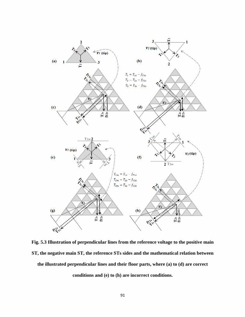
91
Fig. 5.3 Illustration of perpendicular lines from the reference voltage to the positive main
ST, the negative main ST, the reference STs sides and the mathematical relation between
the illustrated perpendicular lines and their floor parts, where (a) to (d) are correct
conditions and (e) to (h) are incorrect conditions.

92
[𝑇1𝑚𝑇2𝑚𝑇3𝑚
] = [111] − [
𝑇1𝑇2𝑇3
] (5.12)
where 𝑇𝑤𝑚 with 𝑤 = 1,2,3, are incorrect calculated on-time durations due to incorrect main ST
selection. The summation of 𝑇𝑤𝑚 in this condition is equal to 2. Hence, when the total summation
of the calculated on-time duration is equal to 2 that means the reference ST and considered main
ST have different type and the calculations should be corrected by changing the main ST type. In
this condition, the value of 𝐶𝑝𝑛 will switch and on-time duration calculations are repeated.
For sake of clarity, consider a second example where the on-time duration calculation details
for different reference voltages are tabulated in Table 5.1. The gray rows are utilized to indicate
the incorrect on-time duration calculations when the main ST type and the reference ST type are
opposite. Followed by the corrected calculations in the next row by switching the 𝐶𝑝𝑛 from 1 to -1
or vice versa.
5.3.4 Switch states
After calculation of the on-time durations, the switching states (𝑆𝑝𝑔ℎ with = 𝑎, 𝑏, 𝑐, ) can be
obtained in the g-h plane (as shown in Fig. 5.2a) [85] by
(𝑆𝑎𝑔ℎ, 𝑆𝑏𝑔ℎ, 𝑆𝑐𝑔ℎ) = (𝑖, 𝑖 − 𝐺, 𝑖 − 𝐺 − 𝐻) (5.13a)
where (𝑖, 𝑖 − 𝐺, 𝑖 − 𝐺 − 𝐻) ∈ {−𝑛−1
2 … , −1, 0, 1, … ,
𝑛−1
2 }, G and H are coordinates of the
reference ST in the g-h plane which are shown by two digit numbers in Fig. 5.2a. With respect to
the introduced formulations in (5.11), G and H for the reference STs are calculated by the
following simple equation
[𝐺𝐻] = 𝐶𝑝𝑛 ( [
0 0 10 1 0
] + 𝑓𝑙𝑜𝑜𝑟 [𝑇3𝑠 𝑇3𝑠 𝑇3𝑠𝑇2𝑠 𝑇2𝑠 𝑇2𝑠
] ) (5.13b)

93
Table 5.1 The on-time duration calculation details based on proposed complementary
SVM method
Hence using (5.11) to find switch on-time durations, the switching states are directly found
using (5.13). That means there is no requirement for pre-computed look-up tables.
After finding the switching states, the switching sequence should be formed by selection and
optimization of the appropriate switching states. Generally, the switching sequence could be
formed for reducing total harmonic distortion [68-69] changing switching frequency [70],
balancing the DC capacitor voltages [71-72], and also for reducing switching losses [73]. The
continuous switching sequence [68] for minimizing the total harmonic distortion level is utilized
here.
5.3.5 The proposed flowchart used in programming of a digital signal processor
Although a significant effort has been expended in the above problem formulation and
simplification of the variable calculations of the proposed complementary SVM method, once the
formulation is complete, the result is highly efficient computation. The simulation or practical
programming tasks for an arbitrary n-level inverter can be executed based on the following simple
and efficient flowchart (Fig. 5.4). Referring to Fig. 5.4, after reading the input data and
considering the pre-default value for 𝐶𝑝𝑛 (pre-default value can be arbitrarily set to 1 or -1), the

94
on-time durations are calculated based on (5.11). Then the total summation of the switch on-time
durations is checked; if the total time is incorrect (unequal to 1) the value of 𝐶𝑝𝑛 will switch and
on-time duration calculations will be repeated. After computing the on-time durations all
switching states are obtained based on (5.13). Then, the switching sequences can be formed based
on the problem specification and objectives [68-73].
The proposed methodology can be extended for a general n-level inverter in a straightforward
manner. Consider a third example with a high number of inverter levels where it is shown that the
calculations are still straightforward: The calculation procedure for a 17-level inverter is
presented here for (5.e2) to (5. e5), with a typical reference voltage with 𝑉𝑥−𝑟𝑒𝑓 = 12.4 and
𝑉𝑦−𝑟𝑒𝑓 = 5.5. Utilizing (5.11) gives
[𝑇1𝑠𝑇2𝑠𝑇3𝑠
] = [0 0.5 10 0.866 01 1 1
]
−1
[12.45.51] = [
−14.5756.35109.2245
] (5.e2)
And subsequently
[𝑇1𝑇2𝑇3
] = [−14.5756.35109.2245
] − 𝑓𝑙𝑜𝑜𝑟 [−14.5756.35109.2245
] = [0.42450.35100.2245
] (5.e3)
The accuracy of calculation can be checked by computing the total summation of the on-time
durations ( ∑ 𝑇𝑤3𝑤=1 = 1). When the total summation of the on-time durations is equal to 1, the
nearest three voltage vectors coordinates in the g-h plane can be obtained by substituting a part of
(5.e3) in (5.13b) as
[𝐺𝐻] = [
0 0 10 1 0
] + [9 9 96 6 6
] = [9 9 106 7 6
] (5.e4)
And finally the switching states are calculated using (5.13a) as (note the iterations of index i)
(𝑆𝑎𝑔ℎ, 𝑆𝑏𝑔ℎ, 𝑆𝑐𝑔ℎ) = (𝑖, 𝑖 − 9, 𝑖 − 9 − 6) = [𝑖=8→ (8,−1,−7) &
𝑖=7→ (7,−2,−8)] (5.e5)

95
Fig. 5.4 The flowchart for programming based on proposed complementary SVM method
(𝑆𝑎𝑔ℎ, 𝑆𝑏𝑔ℎ, 𝑆𝑐𝑔ℎ) = (𝑖, 𝑖 − 9, 𝑖 − 9 − 7) = [𝑖=8→ (8,−1,−8)]
(𝑆𝑎𝑔ℎ, 𝑆𝑏𝑔ℎ, 𝑆𝑐𝑔ℎ) = (𝑖, 𝑖 − 10, 𝑖 − 10 − 6)[𝑖=8→ (8,−2,−8)]
Consider now the extension of example 3 to a 19-level inverter topology, where the on-time
durations and g-h plane coordinates are calculated with same equations (5.e3 to 5.e4) but more
effort is required for calculating the switching states. This means that only equation (5.13a) needs
to be changed as shown here
(𝑆𝑎𝑔ℎ, 𝑆𝑏𝑔ℎ , 𝑆𝑐𝑔ℎ) = (𝑖, 𝑖 − 9, 𝑖 − 9 − 6) (5.e6)
= [𝑖=9→ (9, 0 , −6)&
𝑖=8→ (8,−1 , −7)&
𝑖=7→ (7,−2 , −8)&
𝑖=6→ (6,−3 , −9)]
(𝑆𝑎𝑔ℎ, 𝑆𝑏𝑔ℎ , 𝑆𝑐𝑔ℎ) = (𝑖, 𝑖 − 9, 𝑖 − 9 − 7) = [𝑖=9→ (9, 0 , −7)&
𝑖=8→ (8,−1,−8)&
𝑖=7→ (7,−2,−9)]
(𝑆𝑎𝑔ℎ, 𝑆𝑏𝑔ℎ , 𝑆𝑐𝑔ℎ) = (𝑖, 𝑖 − 10, 𝑖 − 10 − 6) = [𝑖=9→ (9,−1,−7)&
𝑖=8→ (8,−2,−8)&
𝑖=7→ (7,−3,−9) ]
As has been shown in the previous 17-level and 19-level inverter examples, the proposed
complementary SVM method can be extended for a general n-level inverter, without significant
increase in computational complexity (as discussed in more detail later in this chapter), resulting

96
in very simple digital signal processor implementation which is scalable with the number of
inverter levels. Avoiding calculation of the nearest three voltage vectors coordinates should be
considered as the main reason for the improved computational efficiency of the proposed
complementary SVM method. It should be highlighted that the required execution time could be
split into two parts; the first part is calculation of the on-time durations (5.11), checking the
accuracy of the calculation, switching the coefficient if required and subsequently computing the
reference ST coordinates in the g-h plane (5.13b); and the second part is computation of the
switching states (5.13a) which is shown by gray highlight in Fig. 4. The computational burden of
the first part is decreased significantly, compared to that of [126] and other methods in the
literature, based on the proposed method in this chapter. This part of the calculation is
independent of the number of inverter levels (as has been shown in the above examples for a 17-
level and a 19-level inverter). However the computational intensity of the second part, (5.13a),
depends on the number of inverter levels (compare (5.e5) and (5.e6)). In this chapter all
switching states are calculated by (5.13a), and for this reason several loops are used. It should be
mentioned that with an increase of the inverter levels more computational efforts are added to the
processor due to extra computation within each loop. Hence, the execution time for second part of
the calculations, (5.13a), depends on the number of inverter levels.
Referring to the flow chart of Fig. 5.4, it should be noted that looping back (when ( ∑ 𝑇𝑤3𝑤=1 ≠
1)) in the proposed method typically does not occur very frequently (generally much less than
half the time). The proportion of loop back operations decreases as modulation index decreases.
The proportion of loop back operations decreases as switching frequency increases. Even when
loop back is necessary, the computations effort is quite light.

97
5.4 Simulation and Experimental Results
A simulation study in the MATLAB environment and an experimental investigation are
employed to verify performance of the proposed algorithm and to examine its effectiveness in
decreasing the computational overhead in comparison with the conventional SVM method.
A 3-phase 7-level Cascaded H-Bridge (CHB) inverter is considered in the simulation case
study. The sampling frequency and modulation index and voltage for DC sources are: 3600Hz,
0.95 and 1 per-unit, respectively. The inverter line-to-neutral voltages (a, b, and c) are depicted in
Fig. 5.5a, with different colors. The line-to-line inverter voltages (13-level) are depicted in Fig.
5.5b and the generated power from the DC sources (three DC sources in each phase) to each
phase of inverter are depicted in Fig. 5.5c. As illustrated in Fig. 5.5c, the generated powers by all
DC sources are approximately equal to 1 per unit (gray solid line, black diamond and gray square
for first, second and third connected DC sources to each phase). That implies that the switching
redundancy states are distributed properly for the system. The 3-phase load currents and the
output line-to-neutral voltage spectra before filtering are illustrated in Fig. 5.5d. The load current
for the 7-level system (Fig. 5.5d1) has a very good quality as expected for a 7-level inverter. It
should be noted that due to the identical nature of the output waveforms, the voltage spectra (or
the total harmonic distortion) for the proposed complementary SVM method and conventional
SVM method are equal.
The implemented 3-phase 3-level and 3-phase 5-level CHB inverters in experimental set-ups
have been designed using the IRG4BC20UD switching device and the TMS320F2812, a well-
known industrial digital signal processor The sampling frequency, modulation index, voltage for
DC sources and the 3-phase wye connected load (for each phase) are: 3600Hz, 0.95, 70 volt and
37.5Ω, respectively. A current sensor, the ACS714, is utilized to measure the DC source currents

98
(and thus power is found). For ease of the comparisons between different experimental and
simulation cases, per unit values are utilized in all figures.
Experimental results for the 3-phase 3-level CHB inverter are illustrated in Fig. 5.6 with a
similar arrangement as in Fig. 5.5. The inverter line-to-neutral voltages (a, b, and c) and line-to-
line voltages (5-level) are depicted in Fig. 5.6a and Fig. 5.6b, respectively. The generated power
from the DC sources to each phase of the inverter are depicted in Fig. 5.6c. Similar to the
simulation investigation the generated powers by all DC sources are approximately equal to 1 per
unit. That implies that the switching redundancy states are distributed properly for the
system.
Fig. 5.5 Simulation results for the 3-phase 7-level CHB inverter based on the proposed
complementary SVM method a) inverter line-to-neutral voltages b) inverter line-to-line
voltages, c) generated power by DC sources, and d) generated 3-phase output currents and
the output voltage waveform spectra before filtering

99
The 3-phase load currents and the output line-to-neutral voltage spectra before filtering are
illustrated in Fig. 5.6d. The load current for the 3-level system (Fig.5.5) has a small distortion.
The highest harmonic value has the amplitude equal to 18% around frequency 7200Hz.
Experimental results for the 3-phase 5-level CHB inverter system are illustrated in Fig. 5.7. The
utilized arrangements of the depicted sub-figures are compatible with Fig. 5.5 and Fig. 5.6. All
DC sources in the experimental set-ups (6 DC sources) work with approximately equal power of 1
per unit, as seen in Fig. 5.7c (gray solid line and black diamond for first and second connected DC
sources to each phase). As seen in Fig. 5.7d the measured load currents and the output line-to-
neutral voltage spectra before filtering for the 5-level inverter are naturally of higher quality
compared with Fig. 5.6d.
The execution-time for the proposed complementary SVM, the conventional SVM methods
and proposed method in [126], are tabulated in Table 5.2. Note that as the number of inverter
levels is increased, the performance advantage of complementary SVM over conventional SVM
and the proposed method in [126] becomes more significant. All execution times in Table 5.2 are
normalized with respect to the execution time for a 3-phase 9-level inverter based on the proposed
complementary SVM method. For 3-level operation, generally there is about a 35% improvement
in performance, but for 9-level operation with a modulation index of 0.95, the complementary
SVM method is 10.57 times faster than the conventional SVM method. Apparently, when
comparing complementary SVM to conventional SVM, the improvement, with increasing inverter
levels is more dramatic. Compared with the proposed method in [126], for 3-level operation,
generally there is about a 7% improvement in performance, but for 9-level operation with a
modulation index of 0.95, the proposed complementary SVM method is 11% faster than the
proposed method in [126].

100
Fig. 5.6 Experimental results for the 3-phase 3-level CHB inverter based on the proposed
complementary SVM method a) inverter line-to-neutral voltages b) inverter line-to-line
voltages, c) generated power by DC sources, and d) 3-phase output currents and the output
voltage waveform spectra before filtering
It should be highlighted that the required execution time for calculating the switch on-time
durations, checking the accuracy of the calculation, switching of the 𝐶𝑝𝑛 if required, and
computing the reference ST coordinates in the g-h plane is approximately constant. The increase
in the measured computational times is a result of the switching states calculation procedure,
(5.13a). Incidentally, for the proposed complementary SVM, the program for a TMS320F2812
digital signal processor (coded with C++) employed 78 instructions, which is a decrease
compared with [81, 85-86, 126], where [126] uses the same digital signal processor.

101
Fig. 5.7 Experimental results for the 3-phase 5-level CHB inverter based on the proposed
complementary SVM method a) inverter line-to-neutral voltages b) inverter line-to-line
voltages, c) generated power by DC sources, and d) 3-phase output currents and the output
voltage waveform spectra before filtering
Table 5.2 A comparison of SVM execution time (1 per unit time corresponds to 𝟏𝟓. 𝟑𝝁𝒔𝒆𝒄
on a TMS320F2812)

102
5.5 Chapter Summery
A fast and scalable algorithm for computing the SVM variables in a n-level inverter system is
proposed in this chapter. Two main sub-triangles (STs) with constant coordinates are utilized.
These two main STs are referred to in this chapter as the positive main ST and the negative main
ST. A new space vector numbering system is introduced, appropriate for the problem formulation
based on these two main STs in the g-h plane. The parameterized introduced formulations can be
extended to some special conditions (such as non-constant DC sources) very easily. Compared
with other fast SVM methods, the proposed complementary SVM method is the simpler and more
straightforward method for calculating the SVM variables. There are several significant
advantages of the proposed complementary SVM method compared with conventional and other
fast SVM methods. These advantaged are: (i) the proposed procedure for calculation of on-time
durations is independent of the number of inverter levels, (ii) although a 3-phase 7-level problem
has been considered as a running example, the proposed method can be utilized for a general n-
level inverter without any changes in formulation, (iii) there is no limitation for selecting the
modulation index, (iv) compared with all previously published SVM methods, the proposed
complementary SVM method has improved computational efficiency since the conventional
requirement to calculate the nearest three vectors is no longer necessary. Simulation and
experimental verification demonstrate that the proposed complementary SVM method can be
utilized in real time implementations for the general 3-phase n-level inverter.

103
Chapter Six: A FAST AND UNIVERSAL FAULT TOLERANT SPACE VECTOR
MODULATION METHOD FOR THE MULTILEVEL CASCADED H-BRIDGE
INVERTER
6.1 Introduction
Among multilevel inverter topologies [35, 37, 47, 51-58] the Cascaded H-Bridge (CHB)
inverter has gained more attention in medium and high power applications. The main reasons for
this popularity are fewer high power components and modularity of the topology. However, the
operation of a large number of power switching devices in the CHB inverter topology results in
higher probability of failure and a decrease in system reliability. Hence, it is important to
seamlessly transition to reduced power operation under fault conditions. Thus, random occurring
faults should be compensated for in an adaptive manner by fault tolerant approaches [105].
Fault tolerant capability for the multilevel CHB inverter is achieved by redundancies in
hardware [106-107, 141], reconfiguration of the system based on auxiliary components [108], and
also improvement of the modulation and control methods [109-117].
Approaches based on redundancies in hardware can be implemented by: redundant switches
[106] and with redundant H-bridge cells [107]. However additional drive circuits are required and
additional components themselves represent a reliability issue.
A reconfigurable topology with high reliability for the asymmetric multilevel CHB inverter
using an auxiliary multi-winding transformer with bi-directional switches has been proposed in
[108]. However, the additional cost of the auxiliary components is a concern.
Proposed methods for improvement of the modulation and control can be categorized into two
classes: the neutral shift approach [109-111], with recalculation of the required phase shifts in the
104
phase shifted Pulse Width Modulation (PWM) method and, utilizing the switch redundancy states
in the Space Vector Modulation (SVM) approach [112-117].
Regarding the first category, the neutral shift method is proposed in [109] to maximize the
amplitude of the output line-to-line voltage, when the faulty cells (H-bridges) are bypassed by
conductors in the inverter topology. Calculation of the appropriate phase shifts in fault conditions
can be done by solving of a set of non-linear equations. The first attempt to solve these equations
was achieved in [110]. A new method is introduced in [111] to extend the previous work of [110]
and to provide a solution for the fault conditions which lead to multiple solutions or no-solution
based on proposed method in [110]. And finally, a method based on geometrical approach is
proposed in [112].
In the second category, a novel SVM algorithm removes the affected switching states from
Space Vector Diagram (SVD) and generates 3-phase balanced line-to-line voltages based on the
remaining switching states [113-115]. A slightly modified method is introduced in [115-116] to
equalize the switching frequency in normal and fault conditions. Very significantly, the linear
modulation index under fault conditions is increased in [117] by inserting an external DC voltage
source in the inverter configuration.
The main objective of this chapter is to propose a simple and universal fault tolerant SVM
method to improve the multilevel CHB inverter performance under fault conditions. Unlike
existing fault tolerant methods [113-117], to keep continuity in operation of the proposed SVM
approach, the same switching states for both normal and fault conditions are utilized. To achieve
this goal the virtual voltage level concept for the system under fault conditions is defined. This
concept for the healthy topology can be interpreted as an appropriate utilization of the hardware
switching positions to maximize the injected power. However, using the virtual voltage method in

105
fault conditions leads to utilization of the multilevel CHB topology with unequal DC sources. The
space vectors for CHB sub-systems with unequal DC sources are widely distributed. A new
switching sequence with a combination of the 7 and 9 segment sequences and the mean switching
states concept are proposed to compress these widely distributed space vectors. However, a non-
regular hexagon in the SVD is obtained. The complexity of the SVM method associated with this
non-regular hexagon is decreased significantly with extension of the proposed method in [127] for
fault conditions. This proposed method is referred to as the virtual SVM method. Additionally, an
efficient method based on two basic mathematical functions is utilized in conjunction with the
proposed mean switching states concept to find the switching states and to calculate the reduction
in the maximum modulation index for the fault conditions. Furthermore, experimental and
simulation investigations are presented to validate the feasibility of the proposed methods.
The rest of this chapter is structured as follow. The proposed virtual voltage concept is
presented in Section 6.2. Section 6.3 deals with several different presented approaches such as:
the proposed switching sequences, the utilized mean switching states concept, the proposed
virtual SVM method, and the introduced method for calculating the switching states.
Furthermore, a simple formula for calculation of maximum modulation index is also presented in
this section. Simulation and experimental results are provided in Section 6.4. And Section 6.5
presents the chapter summery.
6.2 Proposed Virtual Voltage Concept
One phase of a 7-level CHB inverter topology consisting of 3 H-bridge cells is depicted in
Fig. 6.1. Four different switching positions (this term is used for hardware switching states) are
formed by each cell. Three distinct voltage levels, including positive, zero and negative are
generated by these switching positions. The on and off switching positions are shown in Fig. 6.1

106
with gray and black shading, respectively. The zero level is generated when either upper or lower
switches are in the on position (the middle H-bridge cells in Fig. 6.1b). Hence, there is a
redundant output voltage for the zero level. This surplus position is referred to as a voltage level
redundancy.
In general, 4𝑘 − (2𝑘 + 1) voltage level redundancies can be generated in a series configuration
of k H-bridge cells. As an example, the number of different switch positions for generating a
specific voltage for a 7-level CHB topology in normal (i.e. healthy) conditions is tabulated in the
first column of Table 6.1 (gray font). Correct implementation of these voltage level redundancies
is important to draw the maximum power from the DC sources. For instance, in normal
conditions, there are 6 switching positions for the phase voltage equal to 2pu; three of them are
shown in Table 6.1 in the bolded black box (second column) and three others can be generated
with replacing the ⟨00⟩ switch positions with ⟨11⟩ (both of them correspond to a zero voltage
state). These three different hardware switch positions are depicted in Fig. 6.1. If the calculated
on-time duration based on the proposed SVM method (for generating phase voltage equal to 2pu)
is divided equally among these three switch positions (Table 6.1), all connected DC sources have
identical participation in generating of the phase voltage and subsequently in generating of the
output power. Hence, the total generated power is maximized. This concept is referred to as the
power maximizing concept.
The output power for a 7-level CHB topology with respect to the introduced power maximizing
concept is illustrated in Fig. 6.2a, while operation without power maximizing is shown in Fig.
6.2b. Apparently, the output power by the first method (Fig. 6.2a) is more. Power maximizing is
very important in some applications such as the case of large photovoltaic arrays.
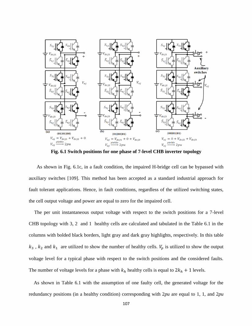
107
Fig. 6.1 Switch positions for one phase of 7-level CHB inverter topology
As shown in Fig. 6.1c, in a fault condition, the impaired H-bridge cell can be bypassed with
auxiliary switches [109]. This method has been accepted as a standard industrial approach for
fault tolerant applications. Hence, in fault conditions, regardless of the utilized switching states,
the cell output voltage and power are equal to zero for the impaired cell.
The per unit instantaneous output voltage with respect to the switch positions for a 7-level
CHB topology with 3, 2 and 1 healthy cells are calculated and tabulated in the Table 6.1 in the
columns with bolded black borders, light gray and dark gray highlights, respectively. In this table
𝑘3 , 𝑘2 and 𝑘1 are utilized to show the number of healthy cells. 𝑉𝑝 is utilized to show the output
voltage level for a typical phase with respect to the switch positions and the considered faults.
The number of voltage levels for a phase with 𝑘ℎ healthy cells is equal to 2𝑘ℎ + 1 levels.
As shown in Table 6.1 with the assumption of one faulty cell, the generated voltage for the
redundancy positions (in a healthy condition) corresponding with 2pu are equal to 1, 1, and 2pu
108
(light gray column). With respect to the power maximizing concept, for which identical on-time
durations should be allocated to each redundancy position, the average output voltage 𝑉𝑝−𝑎𝑣 for
these group of the switch positions is equal to 1.33pu. If all tabulated redundancy positions are
considered, the operation of this phase with one faulty cell can be considered similar to a healthy
phase, but with reduced DC source voltage equal to 0.667pu. In reality, there are two healthy cells
in this phase, and a five level output voltages can be generated. However, utilizing the power
maximizing method and calculating the average voltage 𝑉𝑝−𝑎𝑣 in each switching time interval, a
7-level virtual output voltage can be assumed. Subsequently, a phase with one healthy cell (just
three output level in reality) can be considered virtually similar to a healthy 7-level phase with
DC sources equal to 0.33pu. This proposed method is referred to as the virtual voltage concept.
This proposed concept is extended for the CHB inverter topology with k series cells. A typical
faulty phase of the CHB inverter with 𝑘𝑝 healthy cells can be considered similar to a healthy
system with 2k+1 output voltage levels but with DC source voltages decreased to 𝑘𝑝 𝑘⁄ (𝑝𝑢).
6.3 Proposed Virtual SVM Method
The SVD for a 7-level CHB topology is depicted in Fig. 6.3a. The “a”, “b” and “c” per unit
phase-to-neutral voltage for the space vectors (or switching states) are identified by a three digit
number in the first section of the SVD (Fig. 6.3b). As shown, there are several switch redundancy
states in the SVD (geometry shapes are used in Fig. 6.3 to show the number of redundancies).
Same space vectors with different switching states are constructed by the redundancy states.

109
Table 6.1 Typical voltage level redundancies in a 7-level CHB inverter topology
Fig. 6.2 Effect of appropriate utilization of the voltage level redundancies on output power,
a) proper utilization of redundancies to maximize power, b) minimum switching variations
6.3.1 Proposed switching sequences
Generally, the main task of any SVM method is to use space vectors to represent the reference
voltage. Most often this is accomplished by finding the nearest three vectors to the reference
voltage resulting in a better harmonic profile and lower switch losses (fewer transitions) [70].
With respect to the design objectives, different switching sequences can be formed by the

110
nearest three vectors and their redundancy states. These switching sequences can be split into
continuous and discontinuous forms [68]. The discontinuous switching sequences which can be
provided by three switching states, suffers from higher common mode voltage [70]. To overcome
this negative effect and for sake of expandability of the proposed SVM method as a universal
fault tolerant approach, a new continuous switching sequence with a combination of 7 and 9
segment switching sequences is utilized here. Two switching states form the space vector with
even voltage states (hereinafter called even voltage states) and one switching state form a space
vector with odd voltage states (hereinafter called odd voltage states) are utilized in this proposed
switching sequence. Although there are different choices to select the appropriate switching
states, the best switching performance is obtained by selecting the middle ones [70]. These
considered switching states for Section 1 of the SVD are represented by a 3 digit number with
black shading in Fig. 6.3. Half of the proposed switching sequence for several identified reference
voltages (𝑣1 to 𝑣4 in Fig. 6.3) are shown in periphery of Fig. 6.3. For the illustrated switching
sequences, two utilized redundancies for the even voltage states are highlighted with same colors
(periphery of Fig. 6.3). It is worth mentioning that the second half of the sequence is obtained by
a mirror reflection of the first part.
6.3.2 Proposed mean switching states
The Clarke’s Transformation is utilized to convert the inverter 3-phase output voltage to a
space vector as
𝑉𝑥−𝑞 + 𝑗𝑉𝑦−𝑞 =2
3(𝑉𝑎𝑞 + 𝑉𝑏𝑞𝑒
𝑗2𝜋/3 + 𝑉𝑐𝑞𝑒𝑗4𝜋/3) (6.1)
where 𝑉𝑥−𝑞, 𝑉𝑦−𝑞 and 𝑉𝑝𝑞with 𝑝 = 𝑎, 𝑏, 𝑐 are the real and imaginary part of the space vector
voltage and the inverter phase-to-neutral output voltage, respectively. q is utilized to designate a

111
typical voltage space vector.
It is worthwhile to mention in normal conditions, with the assumption of DC voltage equal to
1pu, the inverter voltage levels are equal to the switching states. For a general case (healthy or
faulty systems), (6.1) may be decomposed into two parts: the first part refers to the switching
states (per unit output voltage in healthy conditions) and the second part is the virtual voltage
vector 𝑉𝑣. Thus the equation is written as
𝑉𝑥−𝑞 + 𝑗𝑉𝑦−𝑞 = [𝑆𝑎𝑞𝐺𝐻 𝑆𝑏𝑞
𝐺𝐻 𝑆𝑐𝑞𝐺𝐻]𝑉𝑣 (6.2)
with 𝑉𝑣 = [𝑘𝑎
𝑘 𝑘𝑏
𝑘𝑒−
𝑗2𝜋
3𝑘𝑐
𝑘𝑒−
𝑗4𝜋
3 ]𝑇
where 𝑆𝑝𝑞𝐺𝐻 and 𝑘𝑝 with 𝑝 = 𝑎, 𝑏, 𝑐, are the switching states and the number of healthy cells in
each phase, respectively.
The inverter switching states can be converted to voltage vectors using (6.2). As an example,
voltage redundancy states and their associated voltage vectors for a 3-phase 7-level CHB
topology in healthy conditions and in two fault cases (one and two faulty cells in phase “a” and
“b”, as a case 1 and one fault for both “a” and “b” phases in case 2) are calculated and tabulated
in Table 6.2. With respect to Table 6.2, in the healthy condition, all switching redundancies are
mapped in the same coordinates (third and eighth row of Table 6.2, depicted with double lines).
However, for fault conditions and considering the virtual voltage concept, the redundancies act
like new space vectors (fourth, fifth and two last rows). Few switch redundancy states for a
healthy system and their corresponding vectors in case 1 are illustrated in Fig. 6.4a. The related
redundancies in case 1 are inscribed with thick black circles. Subsequently, all space vectors for
the case 1 are calculated and illustrated in Fig. 6.4b with black dots over the healthy SVD (gray
lines). As shown, the numbers of voltage vectors is increased significantly. Due to the wide

112
distribution of the space vectors, finding the nearest three voltage vectors to start the SVM
calculations is a very difficult task. This difficulty is mitigated by the proposed mean switching
states method discussed next.
Generally, on-time durations for the nearest three vectors is calculated based on the volt-second
equation as
Fig. 6.3 SVD for a 3-phase 7-level CHB inverter topology
Table 6.2 Effect of virtual voltage on space vector coordinates

113
Fig. 6.4 Comparison between the healthy SVD and widely distributed voltage vectors for
the faulty system ( circles for faulty system and geometry shapes for healthy system)
[𝑉𝑥−1 𝑉𝑥−2 𝑉𝑥−3𝑉𝑦−1 𝑉𝑦−2 𝑉𝑦−31 1 1
] [𝑇𝑟1𝑇𝑟2𝑇𝑟3
] = [
𝑉𝑥−𝑟𝑒𝑓𝑉𝑦−𝑟𝑒𝑓1
] (6.3)
where 𝑇𝑟𝑛 and 𝑉𝑥𝑦−𝑛 with 𝑛 = 1,2,3, are the calculated on-time durations and coordinates of the
nearest three vectors. 𝑉𝑥−𝑟𝑒𝑓 and 𝑉𝑦−𝑟𝑒𝑓 are the reference voltage coordinates.
As mentioned above, for even voltage states, two middle switch redundancy states are utilized
in the proposed switching sequence approach. Hence, the corresponding calculated on-time
duration should be split equally among the redundancies. Equal on-time duration for two
switching states ( space vectors) can be interpreted as a space vector mean calculation. The mean
value for the middles voltage vectors (gray highlighted columns) with respect to the proposed
switching sequence approach is calculated and tabulated in the last column of the Table 6.2 (for
an odd voltage state, the mean value is equal to the middle space vector). Also, the same mean
value will be obtained using all existing switch redundancies in the switching sequence
generation. Hence depending on the application objectives, different switching sequences can be
utilized in the proposed method. Additionally, the virtual voltage vector part of the equation (6.2)
should be considered constant during a specific fault condition. Hence, the proposed mean

114
calculation for the voltage vectors is done just for the switching states and it is simplified as
𝑉𝑥−𝑚 + 𝑗𝑉𝑦−𝑚 = [𝑆𝑎𝑚𝐺𝐻 𝑆𝑏𝑚
𝐺𝐻 𝑆𝑐𝑚𝐺𝐻]𝑉𝑣 (6.4)
[𝑆𝑎𝑚𝐺𝐻 𝑆𝑏𝑚
𝐺𝐻 𝑆𝑐𝑚𝐺𝐻] = {
1
2∑ [𝑆𝑎𝑞
𝐺𝐻 𝑆𝑏𝑞𝐺𝐻 𝑆𝑐𝑞
𝐺𝐻] 𝑓𝑜𝑟 𝑒𝑣𝑒𝑛 𝑣𝑜𝑙𝑡𝑎𝑔𝑒𝑠𝑚+1𝑞=𝑚
[𝑆𝑎𝑞𝐺𝐻 𝑆𝑏𝑞
𝐺𝐻 𝑆𝑐𝑞𝐺𝐻] 𝑓𝑜𝑟 𝑜𝑑𝑑 𝑣𝑜𝑙𝑡𝑎𝑔𝑒𝑠
where 𝑆𝑝𝑚𝐺𝐻 with 𝑝 = 𝑎, 𝑏, 𝑐, are the inverter mean switching states. 𝑉𝑥−𝑚 and 𝑉𝑦−𝑚 are mean
space vector coordinates. With respect to (6.4) the SVM calculation is decomposed into two parts:
calculating the mean switching states, and multiplying this mean value by the virtual voltage
vector.
Generally in SVM methods the switching states are calculated with respect to the space vector
coordinates in the g-h plane. These coordinates are depicted in Fig. 6.5 by two digit numbers. For
the sake of generality the proposed mean switching states calculation with respect to the proposed
switching sequence approach are expressed in the g-h plane as
[
𝑆𝑎𝑚𝐺𝐻
𝑆𝑏𝑚𝐺𝐻
𝑆𝑐𝑚𝐺𝐻
] =1
2[𝐻 + 𝐺 +𝑚𝐻 − 𝐺 +𝑚−𝐻 − 𝐺 +𝑚
] 𝑤𝑖𝑡ℎ 𝑚 = { 0, 𝐺𝐻 ≥ 0
−𝐻, 𝐺𝐻 < 0 𝛿 |𝐺| ≥ |𝐻|
𝐺, 𝐺𝐻 < 0 𝛿 |𝐺| < |𝐻| (6.5)
These calculated mean switching sates are shown by a three digit number in Fig. 6.5.
Considering different fault scenarios and multiplying the generated virtual voltage vector by the
proposed mean switching states, the SVD configuration is obtained for the possible fault
conditions. The SVDs for different fault scenarios are illustrated in Fig. 6.6 (part 1). The
distributed voltage vectors under fault conditions (Fig. 6.4b) are compressed utilizing the
proposed mean switching states concept. The number of redundancies is shown by a dot and a star
for odd and even voltages, respectively.
Note, the SVD for CHB topology under fault conditions is a non-regular hexagon, referred to

115
as the virtual SVD. To do a comparison between this proposed methodology and the conventional
fault tolerant SVM method, the SVDs for the conventional fault tolerant SVM method are
depicted in part 2 of Fig. 6.6. The conventional method is based on removing the effected
switching states and their corresponding space vectors from the SVD [113-117]. It should be
highlighted that for the conventional method, in a given fault condition all switching states,
switching redundancies and switching sequences should be changed. More important, due to the
possibility of a different number of the healthy cells in each phase, the implementation of the
voltage level redundancies in a program for a digital signal processor becomes a complicated
programming task. However the proposed method in this chapter takes advantage from equality
between the switching states and the number of voltage level redundancies for both the healthy
system and the system under fault conditions (Fig. 6.6a). That means no added complexity for
finding the effected vectors or changing the switching sequences in fault conditions. The only
extra complexity is regarding to the calculation of the related SVM variables for the obtained
virtual SVD.
Fig.5 The g-h plane and mean switching states for a 3-phase 7-level CHB inverter

116
Fig. 6.6 Comparison between the SVD for the conventional fault tolerant SVM method and
proposed virtual SVD for different faulty conditions a) healthy condition, b) 1 fault in phase
“a”, c) 3 faults in phase “a”, and d) case 1(see discussion in the text)
6.3.3 Detail Consideration of the proposed virtual SVM method
A fast and universal SVM algorithm is proposed in [127]. All the SVM variable calculations in
this method are done based on the introduction of a main sub-triangle and its complementary sub-
triangle. These two main sub-triangles are called positive and negative main sub-triangles (shown
in Fig. 6.7 as “Positive main sub-triangle 1” and “Negative main sub-triangle 1”). In the proposed
method of [127] the SVM variables are calculated by the following steps: 1) reading the reference
voltage, 2) calculating the on-time durations for the nearest three vectors with respect to positive
and negative main sub-triangle coordinates (without finding the nearest three vectors
coordinates), 3) correction of the calculated on time duration (if required), 4) calculation of the
reference sub-triangle coordinates in the g-h plane, and 5) finding the switching states and

117
constructing of the switching sequence. In this proposed method, the nearest three vectors on-time
durations are calculated by
[𝑇𝑟1 𝑇𝑟2 𝑇𝑟3]𝑇 = [𝑇𝑡1 𝑇𝑡2 𝑇𝑡3]
𝑇 − 𝑓𝑙𝑜𝑜𝑟[𝑇𝑡1 𝑇𝑡2 𝑇𝑡3]𝑇
with [𝑇𝑡1𝑇𝑡2𝑇𝑡3
] = [𝐶𝑝𝑛 [
𝑋𝑚𝑠𝑡𝑧𝑌𝑚𝑠𝑡𝑧
]
[1 1 1]]
−1
[
𝑉𝑥−𝑟𝑒𝑓𝑉𝑦−𝑟𝑒𝑓1
] (6.6)
where 𝑇𝑟𝑛 and 𝑇𝑡𝑛with 𝑛 = 1,2,3, are the calculated on time duration for the reference sub-
triangle and the main sub-triangle respectively. 𝐶𝑝𝑛 is equal to 1 and -1 for positive and negative
reference sub-triangles. 𝑋𝑚𝑠𝑡𝑧 and 𝑌𝑚𝑠𝑡𝑧 are the main positive sub-triangle coordinates.
The simplicity in calculation of the SVM variables of the proposed method in [127] is
obtained from symmetry associated with the healthy SVD configuration in all six sections of the
SVD. However, in fault conditions a non-regular hexagon (virtual SVD) with three different pairs
of sections are obtained. As a running example, the virtual SVD for case 1 is depicted in Fig. 6.7.
For the sake of clarity three different pairs of sections in the SVD are shaded with different
colors. It should be emphasized that all depicted sub-triangles in a given section have identical
dimensions. Given the three different pairs of sub-triangles for the method introduced in [127] it
is possible to extend the technique here utilizing three main sub-triangles for the first three
sections instead of one unique main sub-triangle. In the proposed extended method the sub-
triangles connected to the center of the hexagon in the first three sections are considered as
positive main sub-triangles, while the negative (complementary) main sub-triangle coordinates
are obtained with reflection of the positive main sub-triangle coordinates into center of the
hexagon. Also, similar to the main sub-triangle the reference sub-triangles are categorized as
positive and negative types. For instance, in the section 1 dark gray shading corresponds to the
positive type and vertical hachure corresponds to the negative type reference sub-triangle.

118
In order that the proposed method be adaptable under faulty conditions, the introduced three
main sub-triangle coordinates are computed from the first section point of view and with respect
to the number of healthy cells. These coordinates are obtained with substituting the considered
three main sub-triangle mean switching states in (6.4), coordinates calculations and projection of
the obtained results to the first section. The obtained results are tabulated in Table 6.3. In this
table 𝑋𝑚𝑠𝑡𝑧 and 𝑌𝑚𝑠𝑡𝑧, with 𝑧 = 1,2,3, are used to indicate the first three main sub-triangle
coordinates. Additionally, for a faulty system, the section angular spacing depends on the number
of healthy cells (unequal to 60°). This dependency is shown in Fig. 6.7. Also, an appropriate
formula for calculating the angular spacing 𝜃𝑧 is shown in Table 6.3. As a numerical example, the
three main sub-triangle coordinates and angular spacing for the considered fault condition of case
1 are calculated and tabulated in Table 6.4.
Hence, the introduced SVM method of [127] is adapted here for faulty system including section
recognition with respect to 𝜃𝑧 and selection of the appropriate main sub-triangle coordinates with
respect to the section. Numerical examples for several typical voltage vectors for faulty systems
in case 1 are summarized in Table 6.4. The gray shaded row shows incorrect calculation when the
type of reference sub-triangle and main sub-triangle are different. The proposed method can be
extended for a general n-level CHB topology with no additional computational burden.
Calculation details for a 15-level inverter whit 3 , 8 and 0 faulty cells for phase “a”, “b” and “c”,
are shown in Table 6.4 for rows with bolded borders.
6.3.4 Proposed method to find the switching states
After calculation of the on-time durations the nearest three vector coordinates in the g-h plane
are calculated based on the following formula [127]

119
[𝐺𝐻] = 𝐶𝑛𝑝 ( [
0 0 10 1 0
] + 𝑓𝑙𝑜𝑜𝑟 [𝑇𝑡3 𝑇𝑡3 𝑇𝑡3𝑇𝑡2 𝑇𝑡2 𝑇𝑡2
] ) (6.7)
Then the introduced mean switching states are calculated by (6.5). After calculating the mean
switching states the appropriate switching states for constructing the proposed switching
sequences are obtained by two simple mathematical functions. The middle switching states are
split into upper middle and lower middle switching states. These switching states are calculated
by the ceiling function and floor function from (6.5) as
𝑢𝑝𝑝𝑒𝑟 𝑚𝑖𝑑𝑑𝑙𝑒 𝑠𝑤𝑖𝑡𝑐ℎ𝑖𝑛𝑔 𝑠𝑡𝑎𝑡𝑒𝑠 = 𝑐𝑒𝑖𝑙𝑖𝑛𝑔[𝑆𝑎𝑚𝐺𝐻 𝑆𝑏𝑚
𝐺𝐻 𝑆𝑐𝑚𝐺𝐻] (6.8)
𝑙𝑜𝑤𝑒𝑟 𝑚𝑖𝑑𝑑𝑙𝑒 𝑠𝑤𝑖𝑡𝑐ℎ𝑖𝑛𝑔 𝑠𝑡𝑎𝑡𝑒𝑠 = 𝑓𝑙𝑜𝑜𝑟 [𝑆𝑎𝑚𝐺𝐻 𝑆𝑏𝑚
𝐺𝐻 𝑆𝑐𝑚𝐺𝐻]
It is worth mentioning that for odd redundancies, both floor and ceiling function are mapped
into the same switching states. Finally, these switching states are arranged for generating the
switching sequences. A few numerical examples are shown in Table 6.4 (three last columns).
Hence, the switching states for the proposed sequences are obtained with very simple operations.
Fig. 6.7 a) virtual SVD and proposed sub-triangle positions, b) illustration of maximum
modulation index definition

120
Table 6.3 Three main sub-triangle coordinates and their related angular spacing
Table 6.4 Examples of detailed calculation for the proposed virtual SVM approach
6.3.5 Calculation of maximum modulation index
An important parameter of the SVD for a system in a fault condition is the maximum
modulation index. With respect to the research which has been done in [113], the occurrence of
one fault in a typical phase corresponds with removing the last layer of the healthy hexagon in
four related sections of the SVD. A comparison between maximum modulation index for a
healthy SVD and the fault condition of case 1 (virtual SVD) are shown in Fig. 6.7b. Considering
one faulty cell in phase “a” and one faulty cell in phase “b”, one layer of the healthy SVD in
sections 1, 2, 4, and 5 and two layers from sections 3 and 6 should be removed [113]. The

121
maximum allowable modulation index is proportional with the minimum orthogonal depicted
lines length from the center of the hexagon toward the non-regular hexagon sides. Hence the
following formula for calculation of maximum modulation index is obtained as
𝑚𝑖𝑛𝑑𝑒𝑥 =min (𝑘𝑎+𝑘𝑐,𝑘𝑏+𝑘𝑐,𝑘𝑎+𝑘𝑏)
2𝑘 (6.9)
A fast and universal SVM algorithm, appropriate for both healthy and faulty systems is
suggested in this section. Compared with conventional fault tolerant SVM methods this proposed
method has simpler and efficient application and more compatibility with industrial digital signal
processors.
6.4 Simulation and Experimental Results
A set of simulation and experimental results are presented here to investigate the feasibility
and performance of the proposed virtual SVM method for the multilevel CHB inverter topology
under fault conditions. The simulation is done in the MATLAB environment and the proposed
methods are applied to a 3-phase 7-level CHB inverter topology. The sampling frequency in all
cases is equal to 3600Hz. The selected modulation index is equal to 95% of the maximum
allowable modulation index which can be calculated based on (6.9).
Four faults are considered in the simulation study. The first two faults are occurred in phase
“c”, while faults 3 and 4 occur in phase “b”. The four faults take place at time 0.1033, 0.1566,
0.205 and 0.255 second. The inverter phase-to-neutral voltages, line-to-line output voltages, and
the 3-phase output waveform after filtering are depicted in Fig. 6.8a to Fig. 6.8c, respectively (the
black, gray and light gray lines are utilized to indicate phase “a”, “b”, “c” respectively). The
decrease in the output amplitude in Fig. 6.8c is a result of reduction in the maximum modulation
index in the faulty system. The injected power by the DC sources (three sources for each phase),

122
are illustrated in Fig. 6.8d to Fig. 6.8f. The injected power by the healthy cells is equal to 1pu and
the power goes to zero when the fault occurs. Simulation results show that the proposed fault
tolerant approach has the capability to restore the system operation under even very severe fault
conditions with no additional complexity in the computational requirements.
The 3-phase 3-level and 3-phase 5-level CHB inverter topologies are implemented in the
experimental study. But for sake of space limitation just the result for 3-phase 5-level CHB
inverter are brought here. The CHB topologies have been constructed using the IRG4BC20UD
IGBT switching device and TMS320F2812 digital signal processor. As with the simulation
investigation, the sampling frequency is equal to 3600Hz. The selected modulation index is equal
to 92.5% of the maximum modulation index based on (6.9) in each case. The selected DC source
voltage in the experimental study was equal to 70 volts.
Fig. 6.8 Simulation results for a 3-phase 7-level CHB inverter, a) phase voltages with respect
to inverter neutral point, b) line-to-line voltages, c) 3-phase sinusoidal output voltages, d) to
f) injected power by each of the DC sources

123
The performance of the proposed methods for 3-phase 5-level CHB inverter under different
fault conditions is depicted in Fig. 6.9 to 6.12. In the case of a healthy system, the inverter phase-
to-neutral voltages, the line-to-line voltages, and power provided by the six DC sources are
depicted in Fig. 6.9a to Fig. 6.9c, respectively. The sinusoidal output waveform after filtering
which has very good quality is illustrated in Fig. 6.9d. As it can be seen, the supplied power for
all DC sources (Fig. 6.9d) are equal, which indicates appropriate utilization of the proposed power
maximizing concept.
Three different fault conditions are considered: 1) one faulty cell in phase “c”, 2) two faulty
cells in phase “c”, and 3) two faulty cells in phase “c” and one faulty cell in phase “b”. The phase
voltages, the line-to-line voltages and the 3-phase sinusoidal output waveform for these three fault
conditions are illustrated in parts (a) to (c) of the Fig. 6.10 to Fig. 6.12, respectively. The decrease
in the output amplitude in part (c) of the figures is a result of reduction in the maximum
modulation index in the fault conditions. In the second fault scenario the phase “c” is out of the
system completely, however the proposed virtual SVM method has the capability to restore the
system operation and generating the 3-phase output voltage with a good quality. The considered
system in the third fault condition can be assumed as a worst case scenario when half of the
connected H-bridge cells are bypassed by auxiliary switches. Even in this extreme case the output
waveforms shows acceptable quality.
These experimental results suggest that the proposed virtual SVM approach has very effective
performance for systems under different fault conditions.

124
Fig. 6.9 Experimental results for a 3-phase 5-level CHB inverter in healthy condition,
a) phase voltages, b) line-to-line voltages, c) injected power by DC sources , and d) 3-phase
sinusoidal output voltages
Fig. 6.10 Experimental results for a 3-phase 5-level CHB inverter with one faulty cell in
phase “c” a) phase voltages, b) line-to-line voltages and c) 3-phase sinusoidal output voltages

125
Fig. 6.11 Experimental results for a 3-phase 3-level CHB inverter with two faulty cells in
phase “c”, a) phase voltages, b) line-to-line voltages, and c) 3-phase sinusoidal output voltages
Fig. 6.12 Experimental results for a 3-phase 5-level CHB inverter with two faulty cells in
phase “c” and one faulty cell in phase “b”, a) phase voltages, b) line-to-line voltages and,
c) 3-phase sinusoidal output voltages

126
6.5 Chapter Summery
A universal and scalable fault tolerant SVM algorithm is proposed in this chapter. This method
can be extended in a straightforward manner for systems with any number of levels. Instead of
eliminating switching states which have been affected in fault conditions, the virtual voltage level
concept is utilized. In this proposed method the number of voltage levels is considered constant
and the effect of the faults is interpreted as a variation in the average DC source voltages.
Utilizing this concept, results in similar switching states for normal (healthy) and fault conditions.
A new proposed switching sequence with a combination of the 7 and 9 segment sequences and
the proposed mean switching states concept are utilized to compress the widely distributed space
vectors in the complex plane. However, a non-regular hexagon is formed from the transformation
of the mean switching states in the complex plane. The related SVM variable calculations, for this
non-regular hexagon is simplified by a proposed calculation method based on the three main sub-
triangles with fixed coordinates. Furthermore, a general formulation based on switching state
coordinates in the g-h plane is utilized to simplify calculation of: the virtual SVD and the three
main sub-triangle coordinates. These parameters are calculated with respect to the number of
healthy cells for the general n-level CHB inverter topology. In addition, appropriate utilization of
the voltage level redundancies for maximizing the injected power by the DC sources is
investigated. The performance of the proposed method is validated by simulation and by
experimental investigations. Simulation and experimental results demonstrate that the proposed
method has the capability to deal with very severe fault conditions.

127
Chapter Seven: A DYNAMIC SPACE VECTOR MODULATION METHOD FOR POWER
BALANCE CONTROL OF PHOTOVOLTAIC SYSTEMS
7.1 Introduction
In recent years, grid-connected Photovoltaic (PV) systems have attracted attention in medium
power distributed generation [142]. Among the reasons for this interest are: improvements in
manufacturing processes, reduced installation cost [91] and noiseless operation [93]. However, in
a solar array the variation in the generated power among the solar modules is a considerable
problem.
The output power of a solar module depends on solar irradiance, the module temperature and
the electrical load of the module [142, 95]. Also, shading variations, dirt (soiling) variations, and
inherent manufacturing mismatches between the PV modules can be considered as a main reason
for significant variation in I-V and P-V characteristics.
Among proposed PV topologies [95], the multi string topology can be expanded more easily
and has a greater energy harvest, due to the separate DC-DC converters (one maximum power
point tracking unit for each string).
The multiple DC supplies from the multiple strings make the multi-string topology well suited
for implementation in conjunction with the multilevel Cascaded H-Bridge (CHB) structure [50,
95-97, 113]. However, the inverter designer needs to take into account the voltage and power
imbalance problem among DC sources (PV strings), otherwise significant 3-phase sinusoidal
voltage waveform distortion and output power level degradation may result.
To increase the output voltage waveform quality, hybrid CHB inverter topologies and several
appropriate modulation methods are recommended [58, 100, 144-147]. Conversion efficiency is

128
addressed in [102-104] for a single-phase multilevel CHB inverter topology. The issue of non-
constant DC sources is addressed using different topologies and modulation methods as reported
in [147-150]. The problem of imbalanced generated power by each PV string is extended for 3-
phase systems in [96-97]. The proposed method of [96-97] is based on injection of the minimum-
maximum (min-max) voltage sequence into the conventional reference voltage in the phase-
shifted sinusoidal PWM, resulting in imbalanced phase-to-neutral output voltages, but balanced
line-to-line output voltages.
It is worth noting that all proposed methods in the literature to solve the imbalanced power
problem for 3-phase systems are based on sinusoidal PWM. However, the Space Vector
Modulation (SVM) method offers: lower harmonic components, more freedom in using the
redundant switch states and compatibility with industrial Digital Signal Processors (DSP). Hence,
the objective of this chapter is to suggest an advanced SVM method which has the capability to
deal with imbalanced power sources and imbalanced voltage sources for a CHB inverter topology
with any number of levels. Stand-alone or grid connected PV systems are considered as a specific
applications for this proposed modulation method, though there are other applications.
The first contribution of this chapter, to solve the per-cell power mismatch problem, is to
propose a power sharing method among the H-bridge cells, in each phase, based on voltage level
redundancies in the multilevel CHB inverter. The second contribution of this chapter, in the case
of a n-level inverter with non-constant DC sources is a proposed new formulation of the effective
switching states. The third contribution of this chapter is a proposed dynamic SVM method in the
case of non-constant DC sources and its applications for computing the inverter switching states.
Also, an analytical formula for calculating the Maximum Modulation Index (MMI) in the case of
non-constant DC sources is proposed. In addition experimental investigations are provided to

129
evaluate performance of the proposed methods. This evaluation shows that the proposed dynamic
SVM method combined with the proposed power sharing approach of this chapter has the ability
to be utilized as a general SVM method for a system with non-constant voltage and imbalanced
power. As a result, both 3-phase sinusoidal output voltage and injected power by the DC sources
can be controlled by the proposed SVM method for a CHB inverter with any number of levels.
This chapter is organized as follows. All proposed approaches including power sharing
among DC sources, effective switching states, dynamic SVM method, finding the switching states
and calculating of the MMI are presented in Section 7.3. Simulation and experimental results are
represented in Section 7.4. And Section 7.5provides summery for the chapter.
7.2 Outline of the Proposed Approaches
A typical 3-phase n-level CHB inverter topology is depicted in Fig. 7.1. As shown in the figure,
the PV strings are connected to the DC bus through a maximum power point tracking unit
(usually a boost DC-DC converter). The PV strings are decoupled from the inverter by the DC-
DC converters. Hence, the maximum power point tracking units act independently to maximize
the PV array output power [96]. This independent operation results in an intrinsic power and
voltage mismatch among DC sources. It is worth remembering that the DC output voltage of the
maximum power point tracking unit is related linearly to the generated power of the PV string
(power is approximately proportional to voltage).
Generally, two types of power imbalanced can take place in a grid connected photovoltaic
system. These two types are per-cell imbalance and per-phase imbalance [96-97]. The condition,
when a different level of power is delivered by each connected H-bridge cell in a phase is called
per-cell imbalance. Per-phase imbalance occurs when the total delivered power by DC sources to

130
each phase, are unequal among the phases.
In the following section, the per-cell power mismatch is solved by the proposed power sharing
method. Voltage level redundancies of the multilevel CHB topology (power stage) are used to
achieve this goal. Normally, the per-cell power mismatch is the main reason for the per-phase
power and voltage imbalance. The first effect of the per-phase voltage imbalance on the SVM
method is increasing the number of voltage space vectors. Hence, the regular hexagon in Space
Vector Diagram (SVD) cannot be constructed. To compress the voltage vectors a simple and
extendable formulation based on the effective switching states concept is proposed. The second
effect of the per-phase voltage imbalance on the SVM method concurrent utilizing the effective
switching states is construction of a non-regular hexagon in the SVD and its associated
computational complexities for finding the nearest three voltage vectors. To mitigate these
complexities the dynamic SVM method is proposed.
With help of effective switching states and the introduced dynamic SVM method a
computationally efficient formula is proposed for calculating the switching states instead of
regular nested loops approach. And finally a closed form analytical formula is obtained to take
into account reduction in the MMI, which could be considered another effect of the per-phase
voltage imbalance.
7.2.1 Proposed power sharing method
There are k separate DC sources (PV strings) in each phase of 3-phase n-level CHB inverter
topology (Fig. 7.1). Three voltage levels can be generated by each H-bridge cell. These three
voltage levels are generated by four distinct switching configurations. In normal circumstances,
when all DC sources are equal, the total number of voltage levels and the total number of the

131
switching states in each phase are equal to 𝑛 = 2𝑘 + 1 and 4𝑘, respectively. Hence there are
4𝑘 − (2𝑘 + 1) voltage level redundancies [112] in each phase. Equivalent phase voltage with
different switching configurations can be generated by voltage level redundancies. For sake of
clarity, all switching configurations for a 3-phase 5-level CHB inverter are indicated in Table 7.1
(there are two DC sources in each phase of the 3-phase 5-level CHB inverter topology).
For example, in normal circumstances, four different switching configurations can be utilized to
produce an output voltage equal to 1 per unit (see Table 7.1). For the first and second switching
configurations in Table 7.1 (to produce 1 per unit voltage) the second cell output voltage is zero.
Subsequently, for the third and fourth switching configurations the first cell output voltage is
zero. Hence, with the selection of two switching configurations among these four switching
configurations (one from the first two and one from the last two tabulated switching
configurations) the generated power can be shared equally between the first and second H-bridge
cells. For example, when both switching configurations [0,1,1,1] and [1,1,0,1] have equivalent
participation in generation of the phase voltage equal to 1 per unit, the injected output power is
provided equally by 𝑉𝑑𝑐𝑎1 and 𝑉𝑑𝑐𝑎2. In this condition the related calculated on-time duration
for the considered voltage level should be split into two identical parts and each part should be
allocated to one of the abovementioned switching redundancy. This method should be
implemented for all other voltage levels (for example “-1” per unit).
If the proposed power sharing method is utilized for a system with unequal DC sources, then
because of consideration of equal allocated on-time duration for each cell and due to the
corresponding phase current, the injected power by each source is proportional with its DC source
voltage level. Hence, the per-cell power mismatch can be solved by the proposed power sharing
method.

132
Fig. 7.1 Typical 3-phase n-level CHB inverter topology
Table 7.1 Voltage level redundancies for a 3-phase 5-level CHB inverter (phase “a”)
Additionally, due to consideration of the equal on-time duration among voltage level
redundancies, the average output voltage level of each phase can be obtained by a linear
combination of connected DC sources in the phase. The average phase voltage in a general 3-

133
phase n-level CHB inverter including k H-bridge cells in each phase (Fig. 7.1) is given by
𝑉𝑑𝑐ℎ =∑ 𝑉𝑑𝑐ℎ𝑗𝑘𝑗=1
𝑘 (7.1)
where 𝑉𝑑𝑐ℎ and 𝑉𝑑𝑐ℎ𝑗 with ℎ = 𝑎, 𝑏, 𝑐 and with 𝑗 = 1,2, . . , 𝑘 are normalized average voltage of
the non-constant DC sources and the normalized instantaneous voltages of the non-constant DC
sources for phase “h”, respectively. For a system with non-constant DC sources the calculated
average voltage for DC sources is different and it is the main reason for the per-phase power
imbalance phenomenon.
As an example, the output voltage levels for a 3-phase 5-level CHB inverter with non-
constant DC sources equal to 1 and 0.6 per unit is tabulated in Table 7.1 (last two columns). By
applying the power sharing method the performance of this phase corresponds to a 5-level system
with two identical DC sources with voltage of 0.8 per unit. The maximum generated power by
this phase is linear with the average voltage.
Generally, with correct implementation of the power sharing method, the performance of an n-
level CHB inverter topology with k non-constant DC sources in each phase can be considered
identical with an n-level system with k constant DC sources each with a voltage equal to the
average of the DC voltage sources in each phase (Table 7.1).
7.2.2 Proposed effective switching states concept
By considering the average DC voltage concept, the output voltage of a 3-phase n-level
inverter with non-constant DC sources can be transferred to the complex plane via the following
formula [67]
𝑉𝑞 =2
3(𝑉𝑎−𝑞 + 𝛼𝑉𝑏−𝑞 + 𝛼
2𝑉𝑐−𝑞) (7.2)

134
where 𝛼 = −1
2+ 𝑗
√3
2, q is a typical switching state, 𝑉𝑞 is the voltage space vector (coordinates
in complex plane) and 𝑉ℎ−𝑞 with ℎ = 𝑎, 𝑏, 𝑐, is inverter output voltage for each phase.
The inverter output voltages can be decomposed into two parts. One part is related to the CHB
inverter switching states. And the second part is related to per-phase normalized average voltage
of the DC sources. Based on the proposed power sharing method, the relation between phase
output voltage and switching state is given by
𝑉ℎ−𝑞 = 𝑆𝑆ℎ−𝑞 × 𝑉𝑑𝑐ℎ (7.3)
where 𝑆𝑆ℎ−𝑞 with ℎ = 𝑎, 𝑏, 𝑐, are typical switching states for each phase.
Substituting (7.3) into (7.2) and simplifying gives
𝑉𝑞 =2
3[𝑆𝑆𝑎−𝑞 𝑆𝑆𝑏−𝑞 𝑆𝑆𝑐−𝑞][𝑉𝑑𝑐𝑎 𝛼𝑉𝑑𝑐𝑏 𝛼
2𝑉𝑑𝑐𝑐]𝑇 (7.4)
By substituting the inverter output voltages for different switch states in equation (7.4), the
inverter voltage space vectors can be obtained. In the normal condition, a regular hexagon (SVD)
is constructed by connecting the voltage space vectors to each other.
For illustrative purposes, a 3-phase 5-level CHB inverter is considered as a running example of
this study. In the normal condition when two DC sources are equal, a four layer regular SVD
including 𝑛3 = 125 voltage states, split into (𝑛 − 1)3 = 64 redundancy states and 𝑛3 −
(𝑛 − 1)3 = 61 voltage space vectors is the outcome of transferring the inverter output voltages to
the complex plane. This regular SVD is illustrated in Fig. 7.2a. Circles with different radius are
employed to present the number of voltage states. For example in the center of the hexagon we
have one voltage space vector and four redundant voltages (total number of voltage states is equal
to 5). The corresponding switching states of the inverter are represented in Fig. 7.2 with three
digit numbers.

135
The voltage space vectors for two abnormal cases: (𝑉𝑑𝑐𝑎 = 1, 𝑉𝑑𝑐𝑏 = 0.9, 𝑉𝑑𝑐𝑐 = 0.8) and
(𝑉𝑑𝑐𝑎 = 1, 𝑉𝑑𝑐𝑏 = 0.7, 𝑉𝑑𝑐𝑐 = 0.8), are calculated and illustrated in Fig. 7.2b and Fig. 7.2c (dots
over regular SVD), respectively. As shown, the effect of voltage imbalance on the SVD is an
increased number of voltage space vectors. Hence, the hexagon in the SVD cannot be constructed
for these sporadic voltage vectors. To compress the voltage vectors the effective switching states
are proposed.
Ordinarily, in the vast majority of SVM methods, after finding the nearest three vectors with
respect to the reference voltage, the switching sequences should be determined by selection and
arrangement of the appropriate switching states. Normally, the switching sequence could be
formed for reducing total harmonic distortion [68], changing switching frequency [70], reducing
switching losses, and also for balancing the DC capacitor voltages [53]. The continuous switching
sequence [68] for minimizing the total harmonic distortion level is utilized here.
When determining the continuous switching sequences, the calculated on-time durations,
based on the SVM method, should be divided equally among all considered related voltage states
(voltage space vector and its related redundancy states). As an example, all switching states for a
typical reference voltage (dashed line in Fig. 7.2a) and their related switching sequences are
illustrated in Fig. 7.3. Arrows are utilized to show the arrangement of the switching states in Fig.
7.3a. Noted, there are two switching states for the vector 𝑉1 in Fig. 7.3a, the calculated on-time
duration for the 𝑉1 which has been denoted by 𝑇1 (Fig. 7.3b), are divided equally among these
two switching states for generating the switching sequence.
Considering the equal on-time duration for all voltage states, a given voltage vector can be
interpreted as an effective voltage. Hence, the effective voltages are defined as
𝐸𝑓𝑓 (𝑉ℎ−𝑞1,𝑞2,….𝑞𝑝) = 𝐸𝑓𝑓(𝑆𝑆ℎ−𝑞1,𝑞2,….𝑞𝑝 × 𝑉𝑑𝑐ℎ) (7.5)

136
where “Eff” represents the average calculation, 𝑆𝑆ℎ−𝑞1,𝑞2,….𝑞𝑝 and 𝑉ℎ−𝑞1,𝑞2,….𝑞𝑝 are p different
switching states and their corresponding output voltages, related to the considered voltage vector.
Simplifying of (7.5) gives
Fig. 7.2 a) Regular SVD for a typical 3-phase 5-level CHB inverter topology with equal DC
sources, b) and c) voltage space vectors for two abnormal cases
Fig. 7.3 Switching sequences for a typical reference sub-triangle
137
𝐸𝑓𝑓 (𝑉ℎ−𝑞1,𝑞2,….𝑞𝑝) = 𝐸𝑓𝑓(𝑆𝑆ℎ−𝑞1,𝑞2,….𝑞𝑝) × 𝑉𝑑𝑐ℎ (7.6)
𝑉ℎ−𝑞𝑒 = 𝑆𝑆ℎ−𝑞𝑒 × 𝑉𝑑𝑐ℎ (7.7)
where 𝑆𝑆ℎ−𝑞𝑒 and 𝑉ℎ−𝑞𝑒 with ℎ = 𝑎, 𝑏, 𝑐, are effective switching states and effective inverter
output voltage.
Substituting (7.7) into (7.4) and simplifying gives
𝑉𝑞𝑒 =2
3[𝑆𝑆𝑎−𝑞𝑒 𝑆𝑆𝑏−𝑞𝑒 𝑆𝑆𝑐−𝑞𝑒][𝑉𝑑𝑐𝑎 𝛼𝑉𝑑𝑐𝑏 𝛼
2𝑉𝑑𝑐𝑐]𝑇 (7.8)
where 𝑉𝑞𝑒 is called here the effective voltage space vector.
For the proposed approach, calculation of the effective voltage space vectors can be done in
two steps: calculation of effective switching states and multiplying of the effective switching
states by the weighted average voltage matrix of DC sources. It should be noted that the effective
switching states depend on the CHB inverter level and they can be calculated without dependency
on the DC source voltage variation.
The effective switching states for a 3-phase 5-level CHB inverter are calculated and the
effective voltage space vectors for equal DC sources are illustrated in Fig. 7.4a. It should be noted
that the effective switching sates are shown by a three digit number and the number of utilized
switching states for calculation of effective voltage space vectors is represented by diamonds with
different side lengths. Based on the proposed formula (7.8), the effective voltage space vectors for
the two abovementioned abnormal cases are calculated and illustrated in Fig. 7.4b and 4c (black
color hexagons), respectively. Apparently, the SVD for a multilevel CHB inverter with non-
constant DC sources is a non-regular hexagon.
This non-regular hexagon is referred to as the effective SVD. Basically, depending on the DC
voltage variation, the regular SVD is stretched in one or in two dimensions to construct the

138
effective SVD. This proposed calculation process can be extended, with only a very slight
increase in computation, for a general 3-phase n- level CHB inverter without any difficulty.
Fig. 7.4 Effective SVD for different average DC source voltages, a) Normal condition, b)
The average voltage of selected DC sources are 𝑽𝒅𝒄𝒂 = 𝟏, 𝑽𝒅𝒄𝒃 = 𝟎. 𝟗 and 𝑽𝒅𝒄𝒄 = 𝟎. 𝟖, c)
The average voltage of selected DC sources are 𝑽𝒅𝒄𝒂 = 𝟏, 𝑽𝒅𝒄𝒃 = 𝟎. 𝟕 and 𝑽𝒅𝒄𝒄 = 𝟎. 𝟖
Effective SVD (black shade) is illustrated superimposed over the regular SVD (gray shade)
in part (b) and (c)

139
7.2.3 Proposed dynamic SVM method
As explained in the previous section and due to variation of the DC sources in the
photovoltaic system, the obtained SVD is a non-regular hexagon. This non-regular hexagon can
be split into three similar pairs of sections. Each pair of sections is constructed by identical and
equal sub-triangles (for sake of clarity this non-regular hexagon is decomposed and the
decomposed sections are illustrated in Fig. 7.5).
In general, SVM variable calculation can be considered a complex computational task,
especially for an inverter with more than four levels. This complexity would increase dramatically
in the system with non-constant DC sources. In the last decade several effective SVM methods
[67, 76-79, 82, 86, 126-127] have been proposed for increasing the computational efficiency of
the SVM approach. However, the effect of non-constant DC sources on the SVM variables
calculation is only studied in [126]. It should be noted that the performed study in [126] for 3-
phase 3-level and 3-phase 5-level inverters was a theoretical study based on simulation, without
considering the Maximum Modulation Index (MMI). Due to using a sub-triangle with fixed
coordinates for all SVM variable calculations, extension and practical application of the proposed
method in [126] could be a difficult task. Hence, a new method based on the dynamic main sub-
triangle instead of fixed coordinate sub-triangle [126] is proposed here.
7.2.3.1 Switch on-time duration calculation
Regarding switch on-time calculation and for the sake of scalability and reduction of the
computational burden, a new SVM method based on a dynamic main sub-triangle with variable
coordinates is proposed here. This dynamic main sub-triangle is located in the section where the
reference voltage is placed on it and with one vertex at the origin of the SVD. Therefore,

140
depending on the reference voltage position, there are six different main sub-triangles. The
dynamic coordinates of these main sub-triangles with respect to reference voltage location
(dashed arrowed lines) are shown in Fig. 7.5. These dynamic coordinates can be calculated based
on the obtained effective switching states (7.8) and Fig. 7.4a as follow
[𝑋1𝑚 = 0 𝑋2𝑚 𝑋3𝑚𝑌1𝑚 = 0 𝑌2𝑚 𝑌3𝑚
] = [𝑅𝑒𝑎𝑙(𝑉𝑚𝑠)𝐼𝑚𝑎𝑔(𝑉𝑚𝑠)
] (7.9)
where 𝑉𝑚𝑠 =2
3 [𝑆𝑆1𝑚𝑒 𝑆𝑆2𝑚𝑒 𝑆𝑆3𝑚𝑒]
𝑇[𝑉𝑑𝑐𝑎 𝛼𝑉𝑑𝑐𝑏 𝛼2𝑉𝑑𝑐𝑐]𝑇
and [
𝑆𝑆1𝑚𝑒𝑆𝑆2𝑚𝑒𝑆𝑆3𝑚𝑒
] = (−1)𝑠𝐶𝑖𝑟𝑆ℎ𝑖𝑓𝑡 ([0 0 00.5 −0.5 −0.50.5 −0.5 0.5
] , 𝑠)
where 𝑋𝑡𝑚 and 𝑌𝑡𝑚with t=1,2,3, are the section (dynamic) main sub-triangle coordinates in the
complex plane, 𝑆𝑆𝑡𝑚𝑒 with t=1,2,3, are effective switching states for the section main sub-
triangle. Note that “s” is the section number in which the reference voltage is located and
“𝐶𝑖𝑟𝑆ℎ𝑖𝑓𝑡” is used to show “s” counter clockwise shift of the column in the matrix.
Due to voltage fluctuations the angular distribution of each pair of sections can be different and
not equal to 60° (as shown in Fig. 7.5). The dynamic main sub-triangle coordinates can be used
for calculating the associated angle for each section. These angles can be calculated as:
𝜃𝑠 = tan−1 𝑌2𝑚
𝑋2𝑚− tan−1
𝑌3𝑚
𝑋3𝑚 (7.10)
Normally, all sub-triangles in a section could be categorized as a type 0 or type 1 reference sub-
triangles. The type 0 reference sub-triangles have a direction similar to the section main sub-
triangle; these sub-triangles are shaded with white in Fig. 7.5. The type 1 sub-triangles have 180°
rotation in the direction compared with the section main sub-triangle a shown with black shade in
Fig. 7.5.

141
Fig. 7.5 Decomposed effective SVD and dynamic main sub-triangles coordinates
A general numbering format for obtaining the reference sub-triangle coordinates is utilized
here. In this utilized numbering format the section main sub-triangle is designated with “[1,1]”.
With respect to this numbering format and different selected vertices name for type 0 and type 1
sub-triangle (Fig. 7.5b and 7.5c), the relation between the section main sub-triangle and the
reference sub-triangle coordinates are
[�̂�1𝑚 �̂�2𝑚 �̂�3𝑚�̂�1𝑚 �̂�2𝑚 �̂�3𝑚
] = −1𝑇𝑠 [0 𝑋2𝑚 𝑋3𝑚0 𝑌2𝑚 𝑌3𝑚
] + [𝑋2𝑚(𝑙 − 1) + 𝑋3𝑚(𝑛 − 1)
𝑌2𝑚(𝑙 − 1) + 𝑌3𝑚(𝑛 − 1)] [1 1 1] (7.11)
where �̂�𝑡𝑚 and �̂�𝑡𝑚with t=1,2,3, are the reference sub-triangle coordinates. 𝑇𝑠 is equal to 0 and 1
for type 0 and type 1 reference sub-triangles, respectively. l and n are considered as orthogonal
distances between the section main sub-triangle and the reference sub-triangle.
Based on the above outlined general coordinates formulation, the nearest three voltage vectors
on-time durations can be calculated by volt-second formula [67] as

142
[[�̂�1𝑚 �̂�2𝑚 �̂�3𝑚�̂�1𝑚 �̂�2𝑚 �̂�3𝑚
]
[1 1 1]
] [𝑇1𝑙𝑛𝑇2𝑙𝑛𝑇3𝑙𝑛
] = [
𝑋𝑟𝑌𝑟
1 = 𝑇𝑠𝑝
] (7.12)
where 𝑇𝑡𝑙𝑛 with t=1,2,3, are the calculated on-time durations for reference sub-triangle. 𝑋𝑟 and 𝑌𝑟
are the reference voltage coordinates. 𝑇𝑠𝑝 =1 is the normalized sampling period.
By substituting (7.11) in to (7.12) and simplifying, the following equation is obtained
−1𝑇𝑠 [0 𝑋2𝑚 𝑋3𝑚0 𝑌2𝑚 𝑌3𝑚1 1 1
] [
𝑇1𝑙𝑛𝑇2𝑙𝑛𝑇3𝑙𝑛
] = [𝑋𝑟𝑌𝑟−1𝑇𝑠
] − [𝑋2𝑚(𝑙 − 1) + 𝑋3𝑚(𝑛 − 1)
𝑌2𝑚(𝑙 − 1) + 𝑌3𝑚(𝑛 − 1)0
] (7.13)
Solving (7.13) gives
[𝑇1𝑙𝑛𝑇2𝑙𝑛𝑇3𝑙𝑛
] = −1𝑇𝑠 [0 𝑋2𝑚 𝑋3𝑚0 𝑌2𝑚 𝑌3𝑚1 1 1
]
−1
[𝑋𝑟𝑌𝑟−1𝑇𝑠
] − [2 − 𝑙 − 𝑚𝑙 − 1𝑛 − 1
] (7.14)
The main part of the above mentioned equation can be interpreted as a calculated on-time
duration based on the dynamic main sub-triangle with respect to the reference sub-triangle type,
hence
[0 𝑋2𝑚 𝑋3𝑚0 𝑌2𝑚 𝑌3𝑚1 1 1
]
−1
[𝑋𝑟𝑌𝑟−1𝑇𝑠
] = [𝑇1𝑑𝑚𝑇2𝑑𝑚𝑇3𝑑𝑚
] (7.15)
where 𝑇𝑡𝑑𝑚with 𝑡 = 1,2,3, is the calculated on-time duration based on the dynamic main sub-
triangle.
Whit respect to the presented numbering format, the second part of (7.14) can be interpreted as
a distance between corresponding sides of main and reference sub-triangles [126], [86]. The
relation between these lengths and corresponding calculated on-time durations are given by
[2 − 𝑙 − 𝑚𝑙 − 1𝑛 − 1
] = 𝑓𝑙𝑜𝑜𝑟 (−1𝑇𝑠 [𝑇1𝑑𝑚𝑇2𝑑𝑚𝑇3𝑑𝑚
]) (7.16)

143
Substituting (7.15) and (7.16) into (7.13) and simplifying gives
𝑇𝑡𝑙𝑛 = (−1)𝑇𝑠𝑇𝑡𝑑𝑚 − 𝑓𝑙𝑜𝑜𝑟((−1)
𝑇𝑠𝑇𝑡𝑑𝑚) (7.17)
Considering a normalized sampling period, the summation of the 𝑇𝑡𝑙𝑛 should be equal to 1. If
the summation of the 𝑇𝑡𝑙𝑛 is unequal to 1, that means the considered reference sub-triangle type
(𝑇𝑠) should be changed from 0 to 1 or vice versa.
7.2.3.2 Proposed method for finding switching states
Generally in the SVM method [67] the switching states are calculated in the g-h plane. For this
reason the reference sub-triangle coordinates should be transferred to the g-h plane, and for DSP
implementation the switching states could be computed based on a nested loops method. It should
be noted that with an increased number of inverter levels, a huge computational burden could be
added to the system due to the nested loops. To decrease this complexity a new method for
calculating the switching states based on the introduced effective switching states approach is
proposed here. Using the proposed numbering format for reference sub-triangles, and help of
(7.11) and (7.9), the effective switching states “𝑆𝑆𝑡𝑟𝑒” for the three nearest vectors (with 𝑡 =
1,2,3) can be obtained by
𝑆𝑆𝑡𝑟𝑒 = (−1)𝑇𝑠𝑆𝑆𝑡𝑚𝑒+(𝑙 − 1)𝑆𝑆2𝑚𝑒 + (𝑛 − 1)𝑆𝑆3𝑚𝑒 (7.18)
After calculating of the effective switching states (𝑙 and 𝑛 are calculated above in (7.16)) for
three nearest voltage vectors, all other switching states are calculated by
[𝑆𝑆𝑎−𝑞 𝑆𝑆𝑏−𝑞 𝑆𝑆𝑐−𝑞] = 𝑆𝑆𝑡𝑟𝑒 −max(𝑆𝑆𝑡𝑟𝑒) + 𝑘 − 𝑢
where 0 ≤ 𝑢 < 𝑛 − (max(𝑆𝑆𝑡𝑟𝑒) − min (𝑆𝑆𝑡𝑟𝑒)) (7.19)
7.2.4 Proposed formula for the maximum modulation index
Another important effective SVD characteristic needing consideration is the effect of a

144
decrease in the Maximum Modulation Index (MMI) in the case of non-constant DC sources. This
fact is illustrated graphically in Fig. 7.4c. Usually, the maximum possible modulation index is
proportional to the radius of the largest circle which can be inscribed within the hexagon (Fig.
7.4c). This largest radius corresponds to the smallest orthogonal line from the center of the
hexagon toward the sides of the hexagon (black dash line in Fig. 7.4c). This smallest orthogonal
line length is obtained based on the calculated normalized average voltage of the non-constant DC
sources. The MMI, in the case of non-constant DC sources is given by
𝑀𝑀𝐼 =1
2∑ 𝑉𝑑𝑐ℎℎ=(𝑎,𝑏,𝑐) −
1
2max (𝑉𝑑𝑐𝑎, 𝑉𝑑𝑐𝑏 , 𝑉𝑑𝑐𝑐) (7.20)
Generally, the required steps for the proposed dynamic SVM method can be summarized as
follow: a) calculating the average voltage of the DC sources in each phase, b) computing the
MMI, c) calculation of the dynamic main sub-triangle coordinates (7.9) with respect to the
reference voltage position, d) computation of the three nearest voltage vectors on-time duration
based on the dynamic main sub-triangle coordinates without the need to find the nearest voltage
vectors (7.17), e) verification of the calculated on-time durations (if ∑ 𝑇𝑡𝑙𝑛 ≠ 13𝑡=1 the type of
reference sub-triangle should be changed), f) calculation of the effective switching states for three
nearest vectors (7.18), and g) computing of the switching states and sequences.
Obviously, due to non-constant DC sources, calculation of the SVM variable should be
considered as a very complex task, however this complex calculation is simplified by introducing
a new formulation for effective switching states concurrent with utilizing the dynamic main sub-
triangles. Utilizing theses two ideas eliminates the need to find the three nearest voltage vectors
and avoids a complicated computation. In addition the proposed method for calculation the
switching states based on the proposed effective switching states is completely different and much
more effective compared with utilizing the g-h plane coordinates and nested loops (common

145
method in the literature [126],[86]). Therefore the proposed dynamic SVM can be utilized for the
general n-level CHB inverter without increase in computational complexity.
7.3 Simulation and Experimental Results
A set of simulation and experimental results for 3-phase multilevel CHB inverters with non-
constant DC sources and imbalanced input power levels are presented here to investigate the
feasibility and performance of the proposed methods. The simulation is done in the MATLAB
environment and the proposed technique is applied to voltage and power control of a 3-phase 7-
level CHB inverter with sampling frequency equal to 3600Hz.
Simulation case study results are depicted in Fig. 7.6. The selected normalized DC voltages
and calculated MMI for the utilized 3-phase 7-level CHB inverter are tabulated in Table 7.2. The
inverter calculated line-to-line voltage based on the proposed dynamic method and conventional
SVM method are illustrated in Fig. 7.6a and Fig. 7.6b, respectively. The obtained 3-phase (line-
to-line) sinusoidal waveform for the proposed dynamic method and conventional SVM method
are depicted in Fig. 7.6c1 and Fig. 7.6c2, respectively. Compared with the conventional SVM
method (Fig. 7.6c2), although there are significant variations in input DC voltages, the generated
3-phase sinusoidal output voltage based on the proposed dynamic SVM (Fig. 7.6c1), has
negligible phase variation.
The 3-phase voltage (phase-to-neutral) after filtering and equivalent injected min-max sequence
based on the dynamic SVM method is illustrated in Fig. 7.6d. Variation in phase voltage (Fig.
7.6d1) shows that the equivalent injected min-max sequence by the proposed effective SVM
method is related to the instantaneous voltage of the DC sources.

146
Table 7.2 DC voltages, MMI and total power for considered CHB in simulation
Pro. = Proposed SVM method, Con. = Conventional SVM method
Fig. 7.6 Simulation results for 3-phase 7-level CHB inverter, a) inverter output line-to-line
voltage based on dynamic SVM method, b) inverter line-to-line voltage based on
conventional SVM, c) generated 3-phase sinusoidal waveform based on proposed dynamic
SVM method and conventional SVM method, d) phase voltage after filtering and injected
min-max sequence, e) generated output power for each DC sources based on proposed idea,
and f) generated power for each DC sources based on conventional SVM strategy

147
The injected input power based on the proposed dynamic SVM method and conventional
method for each of the DC sources is depicted in Fig. 7.6e and Fig. 7.6f. Based on theoretical
issues which are discussed in this chapter, the injected power by DC sources should be
proportional with their voltages. This fact is proven in Fig. 7.6e. The summation of the injected
powers, 𝑃𝑡−𝑝𝑟𝑜, by DC sources based on the proposed method, in (Table 7.2) is more than the
corresponding injected power, 𝑃𝑡−𝑐𝑜𝑛, based on the conventional SVM method. These results
show the imbalance power and voltage phenomena can be effectively handled by the proposed
dynamic SVM method.
Experimental set-ups are employed for 3-phase 3-level and 3-phase 5-level CHB inverter
topologies (due to space limitations just the 5L results are shown here), which are designed using
the IRG4BC20UD switching device. The TMS320F2812, an industrial DSP, is utilized to
calculate the dynamic SVM variables. The selected sampling frequency for all experimental tests
is equal to 3600Hz. The maximum voltage for the DC sources is equal to 70 volts, which is
considered as the base voltage for all experimental results. A 3-phase wye connected load, having
a constant resistance of 37.5Ω in each phase, is used for all experimental tests. All measured and
calculated variables are presented in per unit quantities.
The experimental case study results for the 3-phase 5-level CHB inverter are depicted in Fig.
7.7. The normalized input DC sources for this case study are: 𝑉𝑑𝑐𝑎1 = 1, 𝑉𝑑𝑐𝑎2 = 1, 𝑉𝑑𝑐𝑏1 =
0.9, 𝑉𝑑𝑐𝑏2 = 0.4, 𝑉𝑑𝑐𝑐1 = 1, 𝑉𝑑𝑐𝑎2 = 0.9, with modulation index equal to 95% of the maximum
allowable modulation index for the effective SVD configuration.
The inverter line-to-line voltages and 3-phase sinusoidal output waveforms based on the
proposed dynamic SVM method and conventional SVM method are depicted in Fig. 7.7a to Fig.
7.7c. The obtained sinusoidal waveform based on the proposed SVM method, Fig. 7.7c1, has a

148
high quality compared with the conventional SVM method Fig. 7.7c2 (a voltage variation of 25%
can be seen in this condition).
Fig. 7.7 Experimental results for 3-phase 5-level CHB inverter, a) inverter output line-to-line
voltage based on dynamic SVM method, b) inverter line-to-line voltage based on
conventional SVM, c) generated 3-phase sinusoidal waveform based on proposed dynamic
SVM method and conventional SVM method, d) phase voltage after filtering and injected
min-max sequence, e) generated output power for each DC sources based on proposed
dynamic SVM method, and f) generated power based on conventional SVM strategy

149
The 3-phase voltage (phase-to-neutral) after filtering is depicted in Fig. 7.7d1. The measured
equivalent min-max voltage sequence based on the proposed dynamic SVM is illustrated in (black
shade) Fig. 7.7d2 compared with injected min-max sequence (gray shade) [96]. As seen, the
injected sequences are approximately equal. These experimental indicate equivalency between the
proposed effective SVD, and phase-shifted PWM with injected min-max sequences [96]. The
injected DC power based on the proposed dynamic SVM to the system by DC sources is
illustrated in Fig. 7.7e. The injected power by DC sources (Fig. 7.7e) is approximately
proportional with the selected voltage for the DC sources. Furthermore, the total injected power
by the DC sources for the dynamic SVM method is around 5.3 per unit compared with 4.7 per
unit injected power for the conventional SVM method (Fig. 7.7e).
7.4 Chapter Summery
A new general SVM method is proposed in this study. The proposed modulation method has
the capability to deal with imbalanced input power and imbalanced DC voltage levels in operation
of the multilevel CHB inverter. The imbalanced power problem can be divided into per-cell and
per-phase power imbalance problems. The per-cell power mismatch problem is solved by a power
sharing method based on appropriate implementation of voltage level redundancies in each phase
of the multilevel CHB inverter topology. It should be noted that the per-cell power mismatch
problem can be the main cause of DC voltage variation in applications where photovoltaic strings
are employed. To deal with the non-constant DC sources the proposed dynamic SVM method is
utilized. The related SVM variable calculations are simplified by the proposed effective switching
states method. With help of this proposed method, the associated SVM calculations can be split
into one constant part related to multilevel CHB inverter switching states and one variable part

150
related to DC source voltage vectors. In addition, an analytical formula is obtained based on a
trigonometric calculation for finding the MMI in the case of non-constant DC sources when
dealing with effective SVD. An experimental investigation is performed to show the effectiveness
of the proposed method in solving the imbalanced power problem. This investigation also shows
the proposed method, referred to as dynamic SVM, has very similar performance compared with
the method based on injection of a min-max voltage sequence [96]. Although much research is
reported in the literature for solving the problem of power variation resulting from non-equal DC
sources, the study of this chapter may be the first one where this problem is solved in general
terms using an SVM approach.

151
Chapter Eight: CONCLUSIONS AND FUTURE WORK
8.1 Conclusions
This dissertation is devoted to applications of power electronics for renewable energy systems.
In this regard the performance of several power electronic based interfaces for microhydro and
photovoltaic systems are evaluated. The main objective of this research -increasing the renewable
system efficiency in harvesting and consuming the maximum possible generated energy - are
achieved by proposing several new approaches. Additionally the dissertation contains a review of
the literature, theoretical development of new concepts, simulation results and experimental case
studies to verify the theoretical approaches taken.
Stand-alone microhydro units based on the self-exited induction generator are popular in
developing countries. However, an electronic controller is required to maintain the quality of the
generated power in an acceptable range. In the conventional ELC configuration a high degree of
stress can be experienced by stator windings and excitation capacitors resulting from chopper
operation. A new ELC topology is proposed and presented in chapter two to reduce this stress.
Decreasing the stator stress may have a direct effect on increasing the induction generator
longevity. It is worthwhile to mention that consumer load patterns in small communities, indicates
that the total dissipated power in the dump load for the ELC is often greater than the total
consumed power by all households of the community. A solution for this problem is presented in
chapters three and four by distributing the controller among households. In this manner a low cost
distributed controller, which is referred to as the Distributed Electronic Load Controller (DELC)
is proposed. Basically, the proposed DELC is used for two purposes: (a) consuming the excess

152
generated power individually by each household, (b) operating to complement powerhouse ELC
operation for voltage and frequency regulation of the SEIG.
One problem associated with the conventional SVM method is the use of complicated
mathematical calculations arising from the use of trigonometric equations in computing the SVM
variables. It is worth mentioning that these trigonometric equations become significantly more
complicated if the number of output levels is greater than four. Therefore, real time computation
becomes dramatically more complicated using an industrial digital signal processor. Hence, a fast
and scalable algorithm for computing the SVM variables in a n-level inverter system is proposed
in chapter five. Compared with other fast SVM methods, the proposed SVM method is simpler
and is a more straightforward method for calculating the SVM variables. Additionally, in the
multilevel inverter applications utilizing of large numbers of power switching devices there is an
increased probability of failure and associated decrease in the system reliability. Hence, restoring
the normal operation in the multilevel inverter applications even with reduced power capacity is
necessary to avoid great productions losses. The proposed method in chapter five has been
extended in chapter six as a universal and simple SVM algorithm to improve the multilevel CHB
inverter performance under faulty conditions. This method can be extended in a straightforward
manner for systems with any number of levels. Besides the fault tolerant capability, in
applications of multilevel inverters in photovoltaic systems, variation in solar module output
voltage can result in reduced inverter power output and inverter output voltage distortion. To deal
with this problem a dynamic SVM method for the 3-phase n-level CHB inverter is introduced in
chapter seven. It should be noted that the power mismatch problem among photovoltaic cells can
be the main cause of DC voltage variation. In this case and compared with general SVM method a
non-regular hexagon is constructed in place of the regular hexagon space vector diagram. The

153
proposed effective switching states with a combination of the proposed dynamic SVM method are
used to drastically reduce the computational intensity.
8.2 Recommendations for Future Work
Future research, as an extension of the research described in the dissertation, is recommended in
the following areas:
1- The proposed DELC methods in chapters 3 and 4 has a very low construction cost, due in
part to the use of the Texas Instruments MSP-430 microcontroller. However, utilizing an
analog controller instead of the employed digital controller has a direct effect on
decreasing the total system cost, simplicity of the maintenance by local technicians and
possibly increasing the popularity of the proposed idea.
2- The proposed method in chapter five which has been extended as a fault tolerant method
in chapter six also can be extended for use with four leg multilevel inverter topologies to
calculate the SVM variables in a 3 dimensional space vector diagram. This would further
increase the degrees of freedom available in meeting design requirements.
3- Arrangement of the switching positions to optimize commutation between the switching
states in generating the virtual voltage has a direct effect on the system THD level in fault
conditions. Hence, study of the commutation between the switching positions to minimize
the number of transaction between switching states for a system under fault condition is
recommended.
4- The linear relation between the voltage level and the output power can be the main reason
for some limitation in general application of the proposed method in chapter seven. This
problem can be solved by adding additional DC-DC converters before the H-bridge cells
or by some software based methods for changing the switching sequences. In this case a

154
combination of several unequal DC sources without any concern about the output power
level can be used in general multilevel CHB configurations. Hence, extension of the
proposed dynamic SVM method for the general case is recommended.

155
REFERENCES
[1] M. Bergner, “Developing Nepal’s Hydroelectric Resources: Policy Alternatives,” Frank
Batten School of Leadership and Public Policy, University of Virginia, USA, Sep. 2013.
[2] A. Zang, H. M. Kimber, and R. Komp, “Renewable energy village power system for remote
and impoverished Himamayan villages in Nepal,” Proceeding in International Conference on
Renewable Energy for Developing Countries, 2006
[3] J. Parikh, “Hardships and health impacts on women due to traditional cooking fuels: A case
study of Himachal Pradesh, India,” Elsevier International Journal of Energy, vol. 39, pp.
7587–7594, 2011
[4] M.B. Malla Thakuri, “Revisiting the need of improved stoves: estimating health, time and
carbon benefits,” South Asian Network for Developmental and Environmental Economics
Working Paper, No. 44-09, Kathmandu, Nepal, Sep. 2009.
[5] L. P. Naeher, K. R. Smith, B. P. Leaderer, L. Neufeld, and D. T. Mage, “Carbon monoxide as
a tracer for assessing exposures to particulate matter in wood and gas cook stove households
of highland Guatemala,” Environmental Science & Technology, vol. 35, pp. 575–581, 2001,
[6] W. J. Martin, R. I. Glass, J. M. Balbus, and F. S. Collins, “A major environmental cause of
death,” Science, vol. 334, no. 605. Pp. 180-181, Oct. 2011.
[7] N. Bruce, E. Rehfuess, S. Mehta, G. Hutton and K. Smith, “Chapter 42: Indoor air pollution-
disease control priorities in developing country,” Washington (DC): World Bank, 2006,
ISBN-10:0-8213-6179-1.
[8] V. Ramanathan, and G. Carmichae, “Global and regional climate changes due to black
Carbon,” Nature Geosciences, vol. 1, no. 4, pp. 221-227, Mar. 2008

156
[9] B. Singh, S. S. Murthy, and S. Gupta, “Analysis and design of electronic load controller for
self-excited induction generators,” IEEE Trans. on Energy Conv., vol. 21, no. 1, pp. 285- 293,
March 2006
[10] T. F. Chan, K. A. Nigim, and L. L. Lai, “Voltage and frequency of self-excited slip-ring
induction generators,” IEEE Trans. on Energy Conv. ,vol. 19, no. 1, pp. 81-87, March 2004
[11] J. Ramirez, and E. Torres, “An electronic load controller for the self-excited induction
generator,” IEEE Trans. on Energy Conv., vol. 22, no. 2, pp. 546-548, June 2007
[12] E. D. Bassett and F. M. Potter, “Capacitor excitation for induction generators,” AIEE
Transactions, vol. 54, no. 5, pp. 540–545, May 1935.
[13] R. Bansal, “Three-phase self-excited induction generators: an overview,” IEEE Trans. on
Energy Conv., vol. 20, no. 2, pp. 292-299, Jun 2005
[14] B. Singh, S. S. Murthy, and S. Gupta, “STATCOM-based voltage regulator for self-
excited induction generator feeding nonlinear loads,” IEEE Trans. on Ind. Electron., vol. 53,
no. 5, pp. 1437-1452, October 2006
[15] Y. K. Chauhan, S. K. Jain, and B. Singh, “A prospective on voltage regulation of self-
excited induction generators for industry applications,” IEEE Trans. on Ind. Appl., vol. 46, no.
2, pp. 720-730, March/April 2010
[16] B. Singh, M. Singh, and A. K. Tandon, “Transient performance of series-compensated
three-phase self-excited induction generator feeding dynamic loads,” IEEE Trans. on Ind.
Appl., vol. 46, no. 4, pp 1271-1280, July/August 2010
[17] L. Wang and J. Y. Su, “Effect of long shunt and short shunt connections on voltage
variations of a self-excited induction generator,” IEEE Trans. on Energy Conv., vol. 12, no. 4,
pp. 368–374, Dec. 1997

157
[18] T. Ahmed, O. Noro, E. Hiraki, and M. Nakaoka, “Terminal voltage regulation
characteristics by static VAR compensator for a 3-phase self-excited induction generator,”
IEEE Trans. on Ind. Appl., vol. 40, no. 4, pp. 978–988, July/August 2004
[19] T. Ahmed, K. Nishida, and M. Nakaoka, “Static VAR compensator-based voltage control
implementation of single-phase self excited induction generator,” IEE proceedings in
Generation Transmission and Distribution, vol. 152, no.2, pp. 145-156, March 2005
[20] B. Singh, S. S. Murthy, and S. Gupta, “Analysis and design of STATCOM based voltage
regulator for self-excited induction generator,” IEEE Trans. on Energy Conv., vol. 19, no. 4,
pp. 783–790, Dec. 2004
[21] R. Bonert and G. Hoops, “Stand alone induction generator with terminal impedance
controller and no turbine controls,” IEEE Power Engineering Society, Summer Meeting,
1990, pp. 28–31
[22] R. Bonert and S. Rajakaruna, “Stand alone induction generator with terminal impedance
controller and no turbine controls,” IEEE Trans. on Energy Conv., vol. 5, no. 1, pp. 33-39,
1990.
[23] B. Singh, S. S. Murthy, and S. Gupta, “Transient analysis of self-excited induction
generator with electronic load controller (ELC) supplying static and dynamic loads,” IEEE
Trans. on Ind. Appl., vol. 41, no. 5, pp. 1194-1204, September/October 2005
[24] R. Bonert and S. Rajakaruna, “Self-excited induction generator with excellent voltage and
frequency control,” IEE Proceedings in Generation, Transmission and Distribution, vol. 145,
no. 1, pp 31 -39, Jan 1998

158
[25] N. P. A. Smith, “Induction generators for stand alone micro – hydro systems,” IEEE
International Conference on Power Electronics, Drives and Energy System For Industrial
Growth, 1996, pp 669 – 673
[26] B. Singh, S. S. Murthy, and Sushma Gupta, “An improved electronic load controller for
self-excited induction generator in micro-hydel applications,” IEEE Industrial Electronics
Society (ECON 2003), Nov. 2-6, 2003, vol. 3, pp. 2741 -2746
[27] T. Ahmed, K. Nishida, and M. Nakaoka, “Advanced control of PWM converter with
variable-speed induction generator,” IEEE Trans. on Ind. Appl., vol. 42, no. 4, pp. 934-945,
July/August 2006
[28] K. H. Youssef, M. A. Wahba, H. A. Yousef and O. A. Sebakhy, “A new method for
voltage and frequency control of stand-alone self-excited induction generator using PWM
converter with variable DC link voltage,” 2008 American Control Conference, Seattle,
Washington, USA, June 11-13, 2008, pp 2486- 2491
[29] H. S. Timorabadi and E. S. Rogers “Voltage source inverter for voltage and frequency
control of a stand-alone self-excited induction generator,” IEEE Canadian Conference on
Electrical and Computer Engineering (CCECE 2006), Ottawa, May 2006, pp. 2241-2244
[30] G. V. Jayaramaiah and B. G. Fernandes, “Novel voltage controller for stand-alone
induction generator using PWM-VSI,” IEEE Industry Application Conference, Tampa,
October 8-12, 2006, pp. 204-208
[31] J. M. Ramirez, and E. Torres, “An electronic load controller for the self-excited induction
generator,” IEEE Power Engineering Society, June 24-28, 2007, Tampa, pp. 1-8
[32] S. S. Murthy, Bhim Singh, Ashish Kulkarni, R.Sivarajan and Sushma Gupta,“ Field
experiences on a novel pico – hydel system using self-excited induction generator and

159
electronic load controller,” IEEE International Conference on Power Electronic and Drive
(PEDS 2003), November 17-20, 2003, vol. 2, pp 842 – 847,
[33] D. Henderson, “An advanced electronic load governor for control of micro hydroelectric
generation,” IEEE Trans. on Energy Conv., vol. 13, no. 3, pp. 300–304,1998,
[34] F. Blaabjerg, Z. Chen, and S. B. Kjaer, “Power electronics as efficient interface in
dispersed power generation systems,” IEEE Trans. on Power Electron., vol. 19, no. 5, pp.
1184–1194, Sep. 2004
[35] J. Rodriguez, L. G. Franquelo, S. Kouro, J. I. Leon, R. C. Portillo, M. A. M. Prats, and M.
A. Perez, “Multilevel converters: An enabling technology for high-power applications,”
Proceeding of the IEEE, vol. 97, no. 11, pp. 1786-1817, Nov. 2009.
[36] J. Rodriguez, S. Bernet, B. Wu, J. Pontt, and S. Kouro, “Multilevel voltage source
converter topologies for industrial medium voltage drives,” IEEE Trans. on Ind. Electron.,
vol. 54, no. 6, pp. 2930-2945, Dec. 2007.
[37] J. Rodriguez, J.S. Lai, F. Z. Peng, “Multilevel inverters: a survey of topologies, controls,
and applications”, IEEE Trans. on Ind. Electron., vol. 49, no. 4, pp. 724–738, Aug. 2002.
[38] S. Kouro, M. Malinowski, K. Gopakumar, J. Pou, L. G. Franquelo,and B. Wu, “Recent
advances and industrial applications of multilevel converters,” IEEE Trans. on. Ind. Electron.,
vol. 57, no. 8, pp. 2553–2580, Aug. 2010.
[39] A. M. Massoud, S. Ahmed, P. N. Enjeti, and B. W. Williams, “Evaluation of a multilevel
cascaded-type dynamic voltage restorer employing discontinuous space vector modulation,”
IEEE Trans. on Ind. Electron., vol. 57, no. 7, pp. 2398–2410, Jul. 2010.

160
[40] M. Hagiwara, K. Nishimura, and H. Akagi, “A medium-voltage motor drive with a
modular multilevel PWM inverter,” IEEE Trans. on Power Electron., vol. 25, no. 7, pp.
1786–1799, July 2010.
[41] L. Maharjan, S. Inoue, and H. Akagi, “A transformerless energy storage system based on a
cascade multilevel PWM converter with star configuration,” IEEE Trans. on Ind. Appl., vol.
44, no. 5, pp. 1621–1630, Sep./Oct. 2008.
[42] W. Song and A. Q. Huang, “Fault-tolerant design and control strategy for cascaded H-
bridge multilevel converter-based STATCOM,” IEEE Trans. on Ind. Electron., vol. 57, no. 8,
pp. 2700–2708, Aug. 2010.
[43] C. Cecati, F. Ciancetta, and P. Siano, “A multilevel inverter for photovoltaic systems with
fuzzy logic control,” IEEE Trans. on Ind. Electron., vol. 57, no. 12, pp. 4115–4125, Dec.
2010.
[44] C. H. Ng, M. A. Parker, R. Li, P. J. Tavner, J. R. Bumby, and E. Spooner, “A multilevel
modular converter for a large, light weight wind turbine generator,” IEEE Trans. on Power
Electron., vol. 23, no. 3, pp. 1062–1074, May 2008.
[45] F. Khoucha, S. M. Lagoun, K. Marouani, A. Kheloui, and M. E. H. Benbouzid, “Hybrid
cascaded H-bridge multilevel-inverter induction-motordrive direct torque control for
automotive applications,” IEEE Trans. on Ind. Electron., vol. 57, no. 3, pp. 892–899, Mar.
2010.
[46] J. S. Lai, F.Z. Peng, “Multilevel converters – a new breed of power converters”, IEEE
Trans. on Ind. Appl., vol. 32, no. 3, pp. 509–517, May./Jun. 1996.
[47] L. M. Tolbert, F. Z. Peng, and T. G. Habetler, “Multilevel converters for large electric
drives,” IEEE Trans. on Ind. Appl., vol. 35, no. 1, pp. 36–44, Jan./Feb. 1999.

161
[48] R. Teodorescu, F. Blaabjerg, J. K. Pedersen, E. Cengelci, S. Sulistijo, B. Woo, and P.
Enjeti, “Multilevel converters-A survey,” in European Power Electronic Conference (
EPE’99), Lausanne, Switzerland, Sep. 1999, pp. 1098-1107.
[49] Z. Du, B. Ozpineci, L. M. Tolbert, and J. N. Chiasson, “DC–AC cascaded H-bridge
multilevel boost inverter with no inductors for electric/hybrid electric vehicle applications,”
IEEE Trans. on Ind. Appl., vol. 45, no. 3, pp. 963–970, May/Jun. 2009.
[50] “Characteristics of the Utility Interface for Photovoltaic (PV) Systems,” IEC 61727 CDV,
2002
[51] A. Nabae, I. Takahashi, and H. Akagi, “A new neutral-point-clamped PWM inverter,”
IEEE Trans. on Ind. Appl., vol. 17, no. 5, pp. 518-523, Sept./Oct. 1981.
[52] T. A. Meynard and H. Foch, B “Multilevel conversion: High voltage choppers and
voltage-source inverters,” in IEEE Power Electronic Specialist Conference, Teledo, June 29 -
July 03, 1992, vol. 1, pp. 397-403.
[53] T. Bruckner, S. Bernet, and H. Guldner “The active NPC converter and its loss balancing
control,” IEEE Trans. on Ind. Elec., vol. 52, no. 3, pp. 855-868, Jun. 2005.
[54] G. Gateau, T. A. Meynard, and H. Foch, “Stacked multicell converter (SMC): Properties
and design,” in IEEE Power Electronic Specialist Conference, Vancouver, Canada, Jun. 17-
21, 2001, vol. 3, pp. 1583–1588.
[55] T. A. Meynard, H. Foch, F. Forest, C. Turpin, F. Richardeau, L. Delmas, G. Gateau, and
E. Lefeuvre, “Multicell converters: Derived topologies,” IEEE Trans. on Ind. Electron., vol.
49, No. 5, pp. 978-987, Oct. 2002.

162
[56] B. P. McGrath, T. Meynard, G. Gateau, and D. G. Holmes, “Optimal modulation of flying
capacitor and stacked multicell converters using a state machine decoder,” IEEE Trans. on
Ind. Electron., vol. 22, no. 2, pp. 508-516, Mar. 2007.
[57] M. Marchesoni, M. Mazzucchelli, and S. Tenconi, “A non conventional power converter
for plasma stabilization,” in IEEE Power Electronic Specialist Conference, Kyoto, Apr. 11-14,
1988, vol. 1, pp. 122-129.
[58] J. Dixon and L. Moran, “High level multistep inverter optimization using a minimum
number of power transistors,” IEEE Trans. on Ind. Electron., vol. 21, no. 2, pp. 330–337,
March 2006.
[59] L. Li, D. Czarkowski, Y. Liu, and P. Pillay, “Multilevel selective harmonic elimination
PWM technique in series connected voltage inverters,” IEEE Trans. on Ind. Appl., vol. 36,
no.1, pp. 160-170, Jan./Feb. 2000.
[60] B. Ozpineci, L. M. Tolbert, and J. N. Chiasson, “Harmonic optimization of multilevel
converters using genetic algorithms,” IEEE Power Electronics Letters, vol. 3, no. 3, pp. 92-
95, Sept. 2005.
[61] Z. Du, L. M. Tolbert, and J. N. Chiasson, “Active harmonic elimination for multilevel
converters,” IEEE Transa. on Ind. Electron., vol. 21, no. 2, pp. 459-469, March 2006.
[62] J. Rodriguez, L. Moran, P. Correa, and C. Silva, “A vector control technique for medium
voltage multilevel inverters,” IEEE Trans. on Ind. Electron., vol. 49, no. 4, pp. 882–888, Aug.
2002.
[63] G. Carrara, S. Gardella, M. Marchesoni, R. Salutari, and G. Sciutto, “A new multilevel
PWM method: A theoretical analysis,” IEEE Trans. on Ind. Electron., vol. 7, no. 3, pp. 497-
505, Jul. 1992.

163
[64] H. W. Van Der Broeck, H. C. Skudelny and G. V. Stanke, “Analysis and realization of a
pulsewidth modulator based on voltage space vectors”, IEEE Transactions on Industrial
Applications, vol. 24, no. 1, pp. 142-150, Jan./Feb. 1988.
[65] V. T. Ranganathan, “Space vector pulse width modulation - a status review,” Sadhana
Academy Proceedings in Engineering Sciences (India), Dec. 1997, vol. 22, part 6, pp. 675-
688,
[66] F. Wang, “Sine-Triangle vs. Space vector modulation for three-level PWM voltage source
inverters,” in IEEE Industrial Application Conference, Rome, Oct. 8-12, 2000, vol. 4, pp.
2482-2488.
[67] N. Celanovic and D. Boroyevich, “A fast space-vector modulation algorithm for
multilevel three-phase inverters,” IEEE Trans. on Ind. Appl., vol. 37, no. 2, pp. 637–641,
March 2001.
[68] Bin Wu, “High power inverters and AC drives,” Wiley/IEEE Press, 2006.
[69] S. Das and G. Narayanan, “Analytical closed-form expressions for harmonic distortion
corresponding to novel switching sequences for neutral-point-clamped inverters,” IEEE
Trans. on Ind. Electron., vol. 61, no.9, pp. 4485-4497, Sep. 2014.
[70] Z. Cheng and B. Wu, “A novel switching sequence design for five-level NPC/H-bridge
inverters with improved output voltage spectrum and minimized device switching frequency,”
IEEE Trans. on Power Electron., vol. 22, no. 2, pp. 2138-2145, Nov. 2007.
[71] S. Busquets-Monge, S. Alepuz, J. Rocabert, and J. Bordonau, “Pulsewidth modulations for
the comprehensive capacitor voltage balance of n-level three-leg diode-clamped converters,”
IEEE Trans. on Power Electron., vol. 24, pp. 1364-1375, no. 5, May 2009.

164
[72] Z. Shu , N. Ding , J. Chen , H. Zhu, and X. He, “Multilevel SVPWM with dc-link
capacitor voltage balancing control for diode-clamped multilevel converter based
STATCOM”, IEEE Trans. on Ind. Electron., vol. 60, no. 5, pp.1884 -1896, May. 2013.
[73] D. Zhao , V. S. S. P. K. Hari , G. Narayanan, and R. Ayyanar, “Space-vector-based
hybrid pulse width modulation techniques for reduced harmonic distortion and switching
loss”, IEEE Trans. on Power Electron., vol. 25, no. 3, pp.760 -774, Mar. 2010.
[74] O. Lopez, J. Alvarez, J. Doval-Gandoy, et al. “Comparison of the FPGA implementation
of two multilevel space vector PWM algorithms”, IEEE Trans. on Ind. Electron., vol. 55, no.
4, pp. 1537–1547, April 2008.
[75] J. Pou, P. Rodriguez, D. Boroyevich, R. Pindado and I. Candela “Efficient space-vector
modulation algorithm for multilevel converters with low switching frequencies in the devices
” in IEEE Power Electronic Specialist Conference, Recife, June 16-16, 2005, pp. 2521-2526.
[76] A. Mohamed A. S., A. Gopinath, and M. R. Baiju, “A Simple Space Vector PWM
Generation Scheme for Any General n-Level Inverter” IEEE Trans. on Ind. Electron., vol. 56,
no. 5,pp. 1649-1656, May 2009
[77] J. H. Seo, C. H. Choi, and D. S. Hyun, “A new simplified space-vector PWM method for
three-level inverters,” IEEE Trans. on Power Elect., vol. 16, no. 4, pp. 545–550, Jul. 2001.
[78] Y. Deng, K. H. Teo, C. Duan,T. G. Habetler, and R. G. Harley, “A fast and generalized
space vector modulation scheme for multilevel inverters,” IEEE Trans. on Power Electron.,
vol. 29, no. 10, October 2014.
[79] A. K. Gupta, A. M. Khambadkone, “A general space vector PWM algorithm for
multilevel inverters, including operation in overmodulation range” IEEE Trans. on Power
Electron., vol. 22, no. 2, pp. 517-526, March 2007.

165
[80] A. Gupta and A. Khambadkone, “A space vector PWM scheme for multilevel inverters
based on two-level space vector PWM,” IEEE Trans. on Ind. Electron., vol. 53, no. 5, pp.
1631–1639, Oct. 2006.
[81] Z. Shu, J. Tang, Y. Guo, and J. Lian, “An efficient SVPWM algorithm with low
computainal overhead for three phase inverters,” IEEE Trans. on Power Electron., vol. 22, no.
5, pp. 1797–1805, Sep 2007.
[82] A. Gopinath, A. Mohamed A. S., and M. R. Baiju, “Fractal based space-vector PWM for
multilevel inverters—A novel approach,” IEEE Trans. on Ind. Electron., vol. 56, no. 4, pp.
1230–1237, Apr. 2009.
[83] S. K. Mondal, J. P. Pinto, and B. K. Bose, "A neural-network based space-vector PWM
controller for a three-level voltage-fed inverter induction motor drive," IEEE Trans. on Ind.
Appl., vol. 38, pp. 660-669,no. 3, May 2002.
[84] A. Bakhshai, G. Joos, P. Jain, and H. Jin, “Incorporating the over modulation range in
space vector pattern generators using a classification algorithm,” IEEE Trans. on Power
Electron., vol. 15, pp. 83-9, no. 1, Jan. 2000.
[85] M. Saeedifard, H. Salighehrad, A. Bakhshai and R. Iravani, “A fast and universal neuro -
based SVM algorithm for multilevel inverters,” in IEEE Applied Power Electronic
Conference, Anaheim, February 25 - March 1, 2007, pp. 1508-1514.
[86] D. Peng, F. C. Lee, and D. Boroyevich, "A novel SVM algorithm for multilevel three-
phase converters,” in IEEE Power Electronic Specialist Conference, Cairns, June 23-27, 2002,
vol. 2, pp. 509- 513.

166
[87] M. Prats, L. Franquelo, R. Portillo, J. Leon, E. Galvan, and J. Carrasco, “A 3-d space
vector modulation generalized algorithm for multilevel converters”, IEEE Power Electron.
Letter, vol. 1, no. 4, pp. 110–114, Dec. 2003.
[88] M. M. Renge, and H. M. Suryawanshi, “Three-dimensional space-vector modulation to
reduce common-mode voltage for multilevel inverter” IEEE Trans. on Ind. Electron., vol. 57,
no. 7, pp. 2324–2331, Jul. 2011
[89] B. Nia Roodsari, “Computationally efficient space vector modulation for multilevel
inverters and improved capacitor voltage control” MSc thesis, University of Calgary, Calgary,
Canada, May. 2012.
[90] B. Nia Roodsari, A. Al-Judi and E. Nowicki “Modified nearest three virtual space-vector
modulation method for improved DC-capacitor voltage control in n-level diode clamped
inverters” IEEE Canadian Conference on Electrical and Computer Engineering, Montreal,
April 29- May 02, 2012, pp. 1-4,
[91] J. M. Carrasco, L. G. Franquelo, J. T. Bialasiewicz, E. Galvan, R. C. PortilloGuisado, M.
A. M. Prats, J. I. Leon, and N.Moreno-Alfonso, “Power-electronic systems for the grid
integration of renewable energy sources: A survey,” IEEE Trans. on Ind. Electron., vol. 53,
no. 4, pp. 1002-1016, Aug. 2006
[92] J. H. Park, J.Y. Ahn, B.H. Cho, and G.J. Yu, “Dual-module-based maximum power point
tracking control of photovoltaic systems,” IEEE Trans. on Ind. Electron., vol. 53, no. 4, pp.
1036-1047, Jun. 2006.
[93] M. C. Cavalcanti, A. M. Farias, K. C. Oliveira, F. A. S. Neves, and J. L. Afonso,
“Eliminating leakage currents in neutral point clamped inverters for photovoltaic systems,”
IEEE Trans. on Ind. Electron., vol. 59, no. 1, pp. 435-443,Jan. 2012

167
[94] S. Busquets-Monge, J. Rocabert, Pedro Rodríguez, S. Alepuz, and J. Bordonau,
“Multilevel diode-clamped converter for photovoltaic generators with independent voltage
control of each solar array,” IEEE Trans. on Ind. Electron., vol. 55, no. 7, pp. 2713-2723, Jul.
2008
[95] S. B. Kjaer, J. K. Pedersen, and F. Blaabjerg, “A Review of Single-Phase Grid-Connected
Inverters for Photovoltaic Modules,” IEEE Trans. on Ind. Appl., vol. 41, no. 5, pp. 1292-1306,
Sep./Oct. 2005
[96] S. Rivera, S. Kouro, B. Wu, J. Leon, J. Rodriguez, and L. Franquelo, “Cascaded H-bridge
multilevel converter multistring topology for large scale photovoltaic systems,” IEEE
International Symposium on Industrial Electronics (ISIE 2011), June 2011, pp. 1837-1844
[97] S. Rivera, B. Wu, S. Kouro, H. Wang, and D. Zhang, “Cascaded H-bridge multilevel
converter topology and 3-phase balance control for large scale photovoltaic systems,” IEEE
International Symposium on Power Electronics for Distributed Generation Systems (PEDG)
2012, pp. 690-697
[98] M. D. Manjrekar, T. A. Lipo, "A hybrid multilevel inverter topology for drive
applications", IEEE Applied Power Electronics Conference and Exposition, 1998. APEC-98.
vol. 2, Feb. 15-19,1998, pp. 523-529
[99] M. D. Manjrekar, T. A. Lipo, “A generalized structure of multilevel power converter,”
IEEE Power Electronic Drives and Energy Systems for Industrial Growth, vol.1, Dec. 1-3,
1998, pp. 62-67
[100] M. Perez, J. Rodriguez, J. Pontt, and S. Kouro, “Power distribution in hybrid multicell
converter with nearest level modulation,” IEEE International Symposium on Industrial
Electronics, Vigo, Spain, Jun. 4-7, 2007, pp. 736–741.

168
[101] B. P. McGrath, D. G. Holmes, “Multicarrier PWM strategies for multilevel inverter,”
IEEE Trans. on Ind. Electron., vol. 49, no. 4, pp. 858-867, Aug. 2002.
[102] O. Alonso, P. Sanchis, E. Gubia, and L. Marroyo, “Cascaded H-bridge multilevel
converter for grid connected photovoltaic generators with independent maximum power point
tracking of each solar array,” IEEE Power Electronic Specialist Conference, PESC-2003, Jun.
15-19, 2003, vol. 2, pp. 731–735.
[103] J. Negroni, F. Guinjoan, C. Meza, D. Biel, and P. Sanchis, “Energysampled data modeling
of a cascade H-bridge multilevel converter for grid-connected PV systems,” IEEE
International Power Electronic Congress, Puebla, Oct. 16-18, 2006, pp. 1–6
[104] E. Villanueva, P. Correa, J. Rodriguez, and M. Pacas, “Control of a single-phase cascaded
H-bridge multilevel inverter for grid-connected photovoltaic systems,” IEEE Trans. on Ind.
Electron., vol. 56, no. 11, pp. 4399-4406, Nov. 2009
[105] H. Behjati and A. Davoudi, “Reliability analysis framework for structural redundancy in
power semiconductors,” IEEE Trans. on Ind. Electron., vol. 60, no. 10,pp. 4376-4386, Oct.
2013
[106] X. Kou, K. A. Corzine, and Y. Familiant, “A unique fault-tolerant design for flying
capacitor multilevel inverter,” IEEE Trans. on Power Electron., vol. 19, no. 4, pp. 531–987,
Jul. 2004
[107] W. Song, and A. Q. Huang, “Fault-tolerant design and control strategy for cascaded h-
bridge multilevel converter-based STATCOM,” IEEE Trans. on Ind. Electron., vol. 57, no. 8,
pp. 2700-2708, Aug. 2010

169
[108] P. Barriuso, J. Dixon, P. Flores, and L. Moran, “Fault-Tolerant Reconfiguration System
for asymmetric multilevel converters using bidirectional power switches,” IEEE Trans. on
Ind. Electron., vol. 56, no. 4, pp. 1300-1306, Apr. 2009
[109] P. Hammond, “Enhancing the reliability of modular medium-voltage drives,” IEEE Trans.
on Ind. Electron., vol. 49, no. 5, pp. 948–954, Oct. 2002
[110] J. Rodriguez, P. Hammond, J. Pontt, R. Musalem, P. Lezana, and M. Escobar, “Operation
of a medium-voltage drive under faulty conditions,” IEEE Trans. on Ind. Electron., vol. 52,
no. 4, pp. 1080–1085, Aug. 2005.
[111] P. Lezana and G. Ortiz, “Extended operation of cascade multicell converters under fault
condition IEEE Trans. on Ind. Electron., vol. 56, no. 7,pp. 2697–2703, Jul. 2009.
[112] F. Carnielutti, H. Pinheiro, and C. Rech, “Generalized Carrier-Based Modulation Strategy
for Cascaded Multilevel Converters OperatingUnder Fault Conditions,” IEEE Trans. on Ind.
Electron., vol. 59, no. 2, pp. 679-689 Feb. 2012
[113] S. Wei, B.Wu, F.U and C.Liu. “A general space vector PWM control algorithm for
multilevel inverters,” Applied Power Electronics Conference and Exposition (APEC), 2003,
pp. 261-267
[114] S. Wei, B.Wu, S. Rizzo, and N. Zargari, “Comparison of control schemes for multilevel
inverter with faulty cells,” IEEE Industrial Electronics Society, IECON, Nov. 2–6, 2004, vol.
2, pp. 1817–1822
[115] P. Correa, M. Pacas, and J. Rodríguez, “Modulation strategies for fault tolerant operation
of H-bridge multilevel inverters,” IEEE International Symposium Industrial Electronic, Jul.
2006, vol. 2, pp. 1589–1594.

170
[116] G. Maragliano, M. Marchesoni, G. Parodi, L. Vaccaro, “A New generalized fault tolerant
space vector modulator for cascaded multilevel converters,” IEEE 37th Annual Conference,
Industrial Electronics Society, 2011, pp. 1069 -1074
[117] M. Aleenejad, H. Iman-Eini, S. Farhangi, “Modified space vector modulation for fault-
tolerant operation of multilevel cascaded H-bridge inverters,” IET Power Electronic, vol. 6,
iss. 4, pp. 742–751, 2013
[118] S. J. Chapman , “Electric Machinery fundamentals,” Forth Edition, Mc Graw Hill Higher
Education, 2005, ISBN 0-07- 246523-9
[119] B. Nia Roodsari, E. P. Nowicki and P. Freere, “A new electronic load controller for the
self-excited induction generator to decrease stator winding stress,” Elsevier, Energy Procedia,
ISES Solar World Congress 2013, vol. 57, pp. 1455-1464
[120] S. M. Gmunder , R. Zah , S. Bhatacharjee , M. Classen , P. Mukherjee, and R. Widmer,
“Life cycle assessment of village electrification based on straight jatropha oil in Chhattisgarh,
India” Elsevier journal of Biomass and Bio energy, vol. 34, no.3,pp. 347-355, 2010
[121] P. Singh, and H. Gundimeda, “Life cycle energy analysis (LCEA) of cooking fuel
sources used in India households,” Energy and Environmental Engineering 2(1): 20-30, 2014
10.13189/eee.2014.020103, http://www.hrpub.org,
[122] B. Nia Roodsari, E. P. Nowicki and P. Freere, “The distributed electronic load controller:
a new concept for voltage regulation in microhydro systems with transfer of excess power to
households,” Elsevier, Energy Procedia, ISES Solar World Congress 2013, vol. 57, pp. 1465-
1474
[123] B. Nia Roodsari, E. P. Nowicki and P. Freere, “An experimental investigation of the
distributed electronic load controller: A New Concept for Voltage Regulation in Microhydro

171
Systems with Transfer of Excess Power to Household Water Heaters” IEEE International
Humanitarian Technology Conference, Canada, Montreal, June 2014, pp.1-4
[124] B. Nia Roodsari, E. P. Nowicki, “Analysis and experimental investigation of the improved
distributed electronic load controller ,” (submitted to IEEE Transactions on Sustainable
Energy)
[125] B. Nia Roodsari,
E. P. Nowicki, D. H. Wood, K. Silwal, and P. Freere, “Distributed
electronic load controller: operation, calibration, and troubleshooting,” (report used in Nepal
related to Grand Challenges Canada – Stars in Global Health project: Small Scale Hydro
Power for Rural Health in Nepal; a copy of this report is provided in Appendix A)
[126] B. Nia Roodsari, E. P. Nowicki, “Fast space vector modulation algorithm for multilevel
inverters and extension for operation of the cascaded h-bridge inverter with non-constant DC
sources,” IET Power Electronics, vol. 6, pp. 1288-1298, Aug. 2013
[127] B. Nia Roodsari, E. P. Nowicki, “An efficient and universal space vector modulation
algorithm for a general multilevel inverter,” (submitted to IEEE Journal of Emerging and
Selected Topics in Power Electronics)
[128] B. Nia Roodsari, E. P. Nowicki, “A dynamic space vector modulation method for power
balance control of photovoltaic systems,” (in preparation for journal submission to the IEEE
Transactions on Power Electronics).
[129] B. Nia Roodsari, E. P. Nowicki, “A fast and universal fault tolerant space vector
modulation methods for the multilevel cascaded h-bridge inverter, (submitted to IEEE Journal
of Emerging and Selected Topics in Power Electronics).

172
[130] B. Ozpieci, L. M. Tolbert, “Simulink implementation of induction machine model- a
modular approach,” IEEE Electrical Machines and Drive Conference (IEMDC 2003), June 1-
4, 2003, vol. 2, pp 728-734
[131] K. Trinadha, A. Kumar, K. S. Sandhu, “Study of wind turbine based SEIG under
balanced/unbalanced loads and excitation,” International Journal of Electrical and Computer
Engineering (IJECE), vol.2, no.3, pp. 353-370, June 2012, ISSN: 2088-8708
[132] S. S. Murthy, O. P. Malik and A. K. Tandon, “Analysis of self excited induction
generator,” proc. IEE, vol.129, no.6, pp. 260-265, 1982.
[133] N. Batt and C. Coates, “Maximizing output power of self-excited induction generators for
small wind turbines,” IEEE Electrical Machines International Conference, Marseille, Sep. 2-5,
2012, pp. 2105-2111
[134] L. Shridhar, B. Singh, C. S. Jha, B. P. Singh, and S. S. Murthy, “Selection of capacitors
for the self regulated short and shunt self excited induction generators,” IEEE Trans. on
Energy Conv., vol. 10, no. 1, pp. 10–17, Mar.1995.
[135] N. A. Ahmed, K. Amei, and M. Sakui, “A new configuration of single-phase symmetrical
PWM AC chopper voltage controller, ” IEEE Trans. on Ind. Electron., vol. 46, no. 5, pp. 942-
952, October 1999
[136] A. V. Oppenheim, A. S. Willsky, and S. Hamid, “Signals and Systems,” Second Edit,
Prentice Hall, 1996, ISBN-13:978-0138147570,
[137] D. Olaru, And D. Floricau, “Design procedure for the input/output filter circuits used for
single phase ac choppers,” U.P.B. Sci. Bull., series C, vol. 69, no. 3, 2007, ISSN 1454-234x
[138] J. G. Kassakian, M. F Schlecht, and G. C. Verghese, “Principles of Power Electronic,”
Addison-Wesley Publication Company, 1991, ISBN 0-201-09689-7

173
[139] L. Wang, C. H. Lee, “A novel analysis of the performance of an isolated self excited
induction generator,” IEEE Trans. on Energy Conv., vol. 12 no. 2, 1997, pp. 109–117.
[140] C. S. Demoulias and P. S. Dokopoulos, “Transient behavior and self-excitation of wind-
driven induction generator after its disconnection from the power grid,” IEEE Trans. on
Energy Conv., vol. 5, no. 2, pp. 272–278, Jun. 1990.
[141] P. Lezana, J. Pou, T. A. Meynard, J. Rodriguez, S. Ceballos, and F. Richardeau, “Survey
on fault operation on multilevel inverters,” IEEE Trans. on Ind. Electron., vol. 57, no. 7, pp.
2207–2218, Jul. 2010
[142] B. Yang, W. Li, Y. Zhao, and X. He, “Design and analysis of a grid-connected
photovoltaic power system,” IEEE Trans. on Power Electron., vol.25, no.4, pp.992-1000,
April 2010.
[143] H. Shao, C. Y. Tsui, andW. H. Ki, “The design of a micro power management system for
applications using photovoltaic cells with the maximum output power control,” IEEE Trans.
on Very Large Scale Integr. (VLSI), vol. 17, no. 8, pp. 1138–1142, Aug. 2009.
[144] M. Farhadi Kangarlu and E. Babaei, “A generalized cascaded multilevel inverter using
series connection of sub multilevel inverter,” IEEE Trans. on Power Electron., vol. 28, no. 2,
pp. 625–636, Feb. 2013.
[145] P. Hu, and D. Jiang, “A Level-Increased Nearest Level Modulation Method for Modular
Multilevel Converters ,”IEEE Trans. on Power Electron., vol. 30, no. 4, April 2015
[146] M. Liserre, A. Pigazo V. G. Monopoli, A. Dell’Aquila, V. M. Moreno, “A generalised
hybrid multilevel modulation technique developed in case of non-integer ratio among the dc-
Link voltages,” IEEE ISIE2005, Dubrovnik, Croatia, vol. 2, June 20-23, 2005, pp. 513 - 518

174
[147] G. Grandi, C. Rossi, D. Ostojic, and D. Casadei, “A new multilevel conversion structure
for grid-connected PV applications,” IEEE Trans. on Ind. Electron., vol. 56, no. 11, pp. 4416-
4426, Nov. 2009
[148] I. Abdalla, J. Corda, and L. Zhang, “Multilevel DC-link inverter and control algorithm to
overcome the PV partial shading,” IEEE Trans. on Power Electron., vol. 28, no. 1, pp. 14-18,
Jan. 2013
[149] J. Chavarría, D. Biel, F. Guinjoan, C. Meza, and J. J. Negroni, “Energy-balance control of
PV cascaded multilevel grid-connected inverters under level-shifted and phase-shifted
PWMs,” IEEE Trans. on Ind. Electron., vol. 60, no. 1, pp. 98-111, Jan. 2013
[150] F. Filho, L. M. Tolbert, Y. Cao, and B. Ozpineci, “Real-time selective harmonic
minimization for multilevel inverters connected to solar modules using artificial neural
network angle generation,” IEEE Trans. on Ind. Appl., vol. 47, no. 5, pp. 2117-2124, Sep.
/Oct. 2011

175
Appendix A: DISTRIBUTED ELECTRONIC LOAD CONTROLLER:
OPERATION, CALIBRATION, AND TROUBLESHOOTING
November, 2013
B. Nia Roodsaria, E. P. Nowicki
a, D. H. Wood
b, K. Silwal
c and P. Freere
c
aDepartment of Electrical and Computer Engineering, University of Calgary, 2500 University Drive NW, Calgary, T2N 1N4,
Alberta, Canada bDepartment of Mechanical and Manufacturing Engineering, University of Calgary, 2500 University Drive NW, Calgary, T2N 1N4,
Alberta, Canada cKathmandu Alternative Power and Energy and Group, Kathmandu, Nepal
(This report used in Nepal related to Grand Challenges Canada – Stars in Global Health project: Small Scale Hydro
Power for Rural Health in Nepal)
A.1 Introduction
The main idea in the Distributed Electronic Load Controller (DELC) unit is transferring the
excess power from a microhydro turbine to a small water heater in a home (there is one DELC in
each home). There should still be a dump load at the generator site to handle excess power of
homes with a water heater that is turned off, and in case of a fault in the transmission line from
the generator. A block diagram of the home electrical system is illustrated in Fig. A.1. The DELC
block can be split into 7 units:
a) DC power supplies
b) Current sensor
c) Microcontroller
d) IGBT drive circuit
e) Digital thermocouple
f) Bi-directional IGBT switches
g) Water heater element
These units and their communication links is illustrated in Fig. A.2. In the following section
these utilized units are discussed in more detail.

176
Important Safety Note: Before doing the tests for sections 2 to 5 below, it is important to
disconnect the following wires external to the DELC box (the DELC terminal block as seen from
outside the DELC is depicted in Fig. A.17): HT (Hot wire to the Thermocouple unit), HI (Hot
wire for the bi-directional IGBT devices) and HH (Hot wire for the Heater element).
A.2 DC Power Supplies
There are two isolated DC power supplies in the DELC. These two DC power supplies are: a
5V supply for feeding the current sensor unit, the microcontroller unit and a part of the IGBT
drive circuit and a 15V supply for feeding the opto-coupler part of IGBTs drive circuit. This
circuit diagram is depicted in Fig. A.3. The performance of this board can be evaluated by
measuring the voltages at provided test points on the main board. These two test points TP1 and
TP2 are shown in Fig. A.3. Important: TP1 (5V supply) and TP2 (15 supply) have separate
grounds (the 5V ground and 15V ground are not connected together), so it is recommended that
TP1 or TP2 oscilloscope measurements be made in oscilloscope differential mode (ie, X minus Y
mode using two scope probes), otherwise the oscilloscope ground-clips or DELC may be
damaged. Alternatively, and preferably, would be the use of high voltage differential isolation
probes. Warning: the 5V ground reference might be connected to earth ground, but only if the
house has an earth ground connection (connected to the G-5 terminal in Fig. A.17), otherwise the
5V ground reference (G-5) is floating. The 15V ground reference (G-15) is always a floating
ground and should never be connected to earth ground.

177
Fig. A.1 Block diagram of the proposed home electrical system
Fig. A.2 Block diagram of the DELC
Fig. A.3 DC power supplies (5V and 15V)

178
A.3 Current Sensor
The current sensor is ACS714 (8 pin DIP) manufactured by Allegero Microsystem. The main
features of this current sensor are:
a) 1.2 mΩ internal sensing resistance
b) 5.0 V, single supply operation
c) 66 to 185 mV/A output sensitivity
d) Output voltage operation for AC or DC current
e) Nearly zero magnetic offset hysteresis
f) Operating temperature range, -40 to 150°𝐶
One problem associated with all industrial current sensors is low level of output sensitivity for
low wattage applications. The allocated power for each household in small communities which
are electrified by micro hydro units is usually between 50W and 200W. For a 200W allocated
power in a 220V system, the output voltage of the ACS714 current sensor will be around
168mVrms (ie, 185mV/A times a current of 0.909Arms). Hence, to increase the sensitivity, a two
stage operational amplifier (Op-Amp) circuit is used to amplify the ACS714 current sensor
output. This configuration including the current sensor and two stage amplifications is depicted in
Fig. A.4. It is worth remembering that, the designed circuit has been equipped with two variable
resistors for adjusting the gain of each operational amplifier based on the allocated power to each
household (ie, the lower the allocated power, the greater the gain). Referring to Fig. A.4, it should
be highlighted that due to the use of a single 5V DC supply voltage instead of a dual voltage
power supply, in the first stage we have amplification and rectification together. For converting
the half wave sinusoidal waveform of stage 1 to a DC output level (used by the microcontroller),
a simple low pass filter has been placed between the first and second stages.

179
For sake of simplicity and for decreasing the design cost, an open loop control system has been
selected for transferring the excess power to the water heater. The household loads can be divided
into two categories. One category consists of the non-water-heater regular loads including
lighting, radio and TV (and power supply for the DELC system). The second category is the
water heater load. The designed open loop controller is based on non-water-heater power or more
precisely, based on the non-water-heater current. This current is measured by the ACS714 current
sensor and is converted to a DC voltage by the two stage Op-Amp circuit, then this analog output
is converted to a digital signal inside the microcontroller. This digital current signal is employed
as a part of the Pulse Width Modulation (PWM) generator that determines the “AC chopper”
duty-cycle of the water heater. The microcontroller in this project is the MPS-430 (discussed
further in the next section). The recommended DC supply voltage level for this microcontroller is
between 1.8V to 3.6V. The circuit board containing the MPS-430 generates a 3.6V power supply
from the 5V input supply. Considering a safety margin, the maximum output voltage of the Op-
Amp circuit should be limited to 3.5V. It is worth remembering that the delivered power to the
water heater is based on the analog DC output voltage of the second stage of the Op-Amp circuit,
so the Op-Amp circuit can play a very important role in efficiency and performance of the whole
system. For this reason three test points are provided for the Op-Amp circuit and shown in Fig.
A.4 as TP3, TP4 and TP5.
A.3.1 Calibration method
If calibration needs be done in the field due to any repair or modification of the DELC system,
the first step is to disconnect the non-water-heater loads from the DELC. A dump load with

180
respect to maximum allocated power to each household should be connected in place of the non-
water-heater load in Fig. A.4. This dump load can be calculated as:
𝑅𝑑𝑢𝑚𝑝 =𝐼𝑛𝑝𝑢𝑡 𝑣𝑜𝑙𝑡𝑎𝑔𝑒 2
𝐴𝑙𝑙𝑜𝑐𝑎𝑡𝑒𝑑 𝑝𝑜𝑤𝑒𝑟
For a 220V AC system with allocated power equal to 200W, this resistor is
𝑅𝑑𝑢𝑚𝑝 =2202
200= 242Ω
Suggested Procedure:
a) Switch off the house main power switch (the HT, HI, and HH external wires should be
disconnected from DELC box terminal block as noted above)
b) Disconnect the non-water-heater loads from the fuse box.
c) The calculated dump load should be connected across terminals HF and N (replacing the
non-water-heater loads).
d) The measured waveform for test point TP3 is a sinusoidal waveform; the amplitude of this
waveform depends on the allocated power and input voltage. This amplitude is not
important for the system performance. As a rough guideline, the expected peak to peak
voltage is roughly 0.5V (about 0.17Vrms). This waveform is illustrated in Fig. A.5
Fig. A.4 Current sensor and Op-Amp circuit (Important note: G-5V is the ground
reference of the 5V DC supply).

181
Fig. A.5 The test point TP3 waveform
Fig. A.6 The expected test point TP4 waveform
Fig. A.7 Distorted waveform, measured from TP4 which is Not desirable
Fig. A.8 The test point TP5 expected waveform
e) The measured waveform for test point TP4 is a half wave sinusoidal waveform. The
amplitude of this waveform can be adjusted by potentiometer VR1 to its maximum no-
distortion level as it depicted in Fig. A.6. Be careful about distorted waveform similar to
the depicted waveform in Fig. A.7. One simple idea to avoid the waveform distortion in
this test, is keeping the maximum voltage amplitude of the TP4 waveform equal to or less
than 4.5V.

182
f) After adjusting of the half sinusoidal waveform amplitude, the amplitude of the analog DC
output can be adjusted by potentiometer “VR2” as measured at test point TP5. It should be
remembered due to operation of the low-power microcontroller (MSP430); this amplitude
should be limited to 3.5V. The expected waveform is shown in Fig. A.8.
A.4 Microcontroller
The selected microcontroller for this project is the MSP-430 LaunchPad. The Texas
Instruments (TI) MSP430 family of processors are low power 16 bits devices. They can be
utilized in low power application such as battery powered devices. Providing the correct
power supply is very important for this family of microcontroller. Although the MPS430 family
requires low current and thus can be operated by batteries or other low current sources, it requires
a specific voltage, and any increase above the maximum recommended voltage can destroy the
IC. Usually microcontrollers manufactured by Microchip and Atmel can tolerate 5V, but the
recommended voltage for the MSP430 is 1.8V to 3.6V. It should be noted that there is a
possibility to damage the IC if the voltage is over 3.9V. Also, the MSP430 devices have been
equipped with an interface which called JTAG. The JTAG interface allows a user to download
and debug the code on the microcontroller with a small number of the pins (data lines). The
utilized number of data pins for MSP430 is 2 compared with 4 or 5 for other microcontrollers. For
this reason a USB port can be used for connection of the MSP430 circuit board to a PC (personal
computer). A standard USB connection includes a 5V DC power supply from the PC. So the
MSP430 board is equipped with an on-board voltage regulator for converting 5V to 3.6V. There
are two test points for the input voltage when the board is connected to an active USB line (ie,
connected in the DELC or connected to a PC). These two test points provided by the MSP430

183
board manufacturer are identified in Fig. A.9 as “+5V” (the 5V DC supply line) and as “G-5V”
(the ground line for the 5V supply). The 5V line can be connected using a jumper, “J1” as shown
in Fig. A.9. The jumper (“J1”) should be removed when you are going to download a new
program into the microcontroller.
A.4.1 Test method
a) The internal DC voltage supply can be measured from the power connector provided by
the MSP430 board manufacturer. Referring to Fig. A.9, TP7 should be at a constant DC
value of 3.6V (the VCC pin) with respect to TP6 (the GND pin). For your information,
the pin between TP6 and TP7 is also connected to GND.
b) Several DIP switches are provided on the main circuit board (connected to MSP430 board
as shown in Fig. A.9). Based on the heater rating and allocated power to the household the
DIP switches can be configured for the desired operation as shown in Table A.1 (“1”
means the MSP430 pin is connected to 3.6V while “0” means the MSP430 pin is
connected to ground). The DIP switch arrangement for a 200W water heater and 200W
allocated power to each household is shown in Fig. A.9. Note that in all cases shown in
Table A.1 (provided the water temperature has not reached the preset maximum
temperature) the allocated power is delivered to the heater in the case that the non-water-
heater household loads are all turned off. Thus the heater element must be rated for a
power equal to or greater than the allocated power.
c) The connection of the Op-Amp circuit and IGBT drive to the microcontroller is done via
two jumpers. These two jumpers, “J2” and “J3” are shown in Fig. A.9. When testing a
new microprocessor code these two jumpers should be removed, and a variable power

184
supply must be connected between test point TP8 and test point TP6 (ground of
microcontroller). It should be remembered that the maximum permitted voltage in this test
is 3.5V. So at the first step is to be sure that the variable power source has been adjusted to
zero volts (then carefully increased). These two test points could be connected to an
oscilloscope (for example channel 1); then the voltage of the variable power supply can be
changed gradually. Basically, increasing the voltage corresponds to increasing in the
consumed power, hence the power to water heater should be decreasing. This task is
accomplished by a reduction of the PWM (pulse width modulation) pulse width. When
increasing the variable power supply voltage, the pulse width of the observed voltage on
the oscilloscope should be decreasing. Several typical figures regarding this test are
illustrated in Fig. A.10. It is worth remembering that the pulse width depends on the
selected heater rating, allocated power to the household, and instantaneous consumed
power level of non-water-heater household loads.
Fig. A.9 The MSP430 microcontroller circuit board and its test points and jumpers and 5pin
dip switch

185
Table A.1 DIP switch arrangements with respect to heater rating and allocated power to a
given household
Fig. A. 10 PWM output wave form of the microcontroller with respect to non-water-heater
household power

186
A.5 IGBT Drive Circuit
The IGBT driver circuit including two “NOT” gates for protection of the MSP430 and one high
speed opto-coupler is depicted in Fig. A.11. The selected high speed opto-coupler, FOD3184,
manufactured by Fairchild Semiconductor, is used for isolation between the high power chopper
circuit and the low power control circuit. This part is ideally suited for high frequency driving of
power MOSFETS or IGBT devices used in switch-mode power converters. The key features of
the FOD3184 are:
a) High noise immunity characteristic
b) Guaranteed operating temperature range of -40°𝐶 to 100°𝐶
c) 3A peak output gate-drive current for medium power IGBT devices
d) Fast switching speed
e) Fast output rise time
f) Wide DC supply operating range (15V to 30V)
A.5.1 Test method
a) The utilized “NOT” gates can be tested, simultaneously with the MSP430 unit test. For
this purpose the second channel of the oscilloscope should be connected to test point
TP10. This test point is shown in Fig. A.11. The observed voltage in the second channel of
the oscilloscope is similar to the first channel (connected to TP9) but with different
amplitude. The amplitude provided by the MSP430 unit is equal to 3.5V (TP9) compared
with a 5V voltage amplitude which can be obtained from TP10.
b) It should be noted that, the reason for utilizing the opto-coupler in this circuit, is providing
isolation between high voltage and low voltage circuits. So, due to the isolated (separated)

187
ground for the opto-coupler and IGBT drive circuit, the opto-coupler output waveform
should be observed when the oscilloscope ground is disconnected from the MSP430
ground or “G-5” ground. After disconnecting the first and second channels of the
oscilloscope from test point TP9 and TP10 and disconnecting the related ground, the
oscilloscope, in X minus Y differential mode, can be connected to the test point TP11. For
the sake of clarity, this test point has been shown in Fig. A.11 with two points to emphasis
the ground of oscilloscope in this test is different from all pervious tests. The measured
output voltage, similar to pervious step (Fig. A.10) with maximum amplitude equal to 15V
can be observed in this test. IMPORTANT NOTE: It is not safe to connect the ground clip
of the oscilloscope probe to the G-15 point (ground for the 15 volt DC supply). Thus, it is
best to use the oscilloscope in X minus Y differential mode.
Fig. A.11 The IGBT drive circuit and its test points

188
A.6 Digital Thermocouple
The selected digital thermocouple for this project is WH7016G, manufactured by Willihi. The
key features of this unit are:
a) Temperature measurement range: -50℃ to 110 ℃
b) Temperature control range: -50℃ to110℃
c) Temperature measurement error: ± 0.5 ℃
d) Sensor Type: NTC (10K/3435)
e) Control accuracy: 1 ℃
f) Working voltage: AC/DC12V AC220V AC110V
g) Required power: <2W
h) Relay contact point current: 7A/220V AC
i) Unit ambient temperature: 0 ℃ to 50 ℃ (we expect the home temperature can drop below
0 ℃)
The wiring diagram of this thermocouple is depicted in Fig. A.12. Based on recommended wiring
practice of the manufacture, the pin numbers 1 and 4 should be shorted and connected to the
Neutral of the AC system. The Neutral line in the DELC box is indicated in Fig. A.17 with the
“N” notation. Pin number 5 of the WH7016G should be wired to the “Hot Thermocouple”
terminal, “HT” of the DELC box terminal block (see Fig. A.17). The pin 2 (this is the switched
output of the thermocouple unit) should be connected the “Hot IGBT” terminal, “HI” of the
DELC terminal block (see Fig. A.17). The NTC sensor (Negative Temperature Coefficient
sensor, see bottom of Fig. A.13) should be installed in the water heater tank (preferably not near
the heater element and also not near the top of tank where the warm water rises) and it should be
wired to pin numbers 8 and 9.

189
A.6.1 Instructions for controlling the temperature
a) When the house main power switch is off, the pins number 5 and number 1 of the
Thermocouple unit should be wired to the DELC box terminal block, “HT” and “N”,
respectively. The DELC terminal block is depicted in Fig. A.17 (HI and HH should be
kept disconnected).
b) Turn on the house main power switch (it is not critical if household loads are
connected or not).
c) Press the “RST” (reset) key to switch on or off the thermocouple. To power on the
unit, just press on the “RST” key momentarily. To power off the unit, the “RST” key
should be pressed and held for three seconds, after that the unit will be off.
d) To enter the temperature control setting press the “SET” key (once), then press the ∆
(up) or ∇ (down) keys to adjust the temperature. The unit can enter the fast adjusting
mode with pressing and holding the ∆ key or the ∇ key for three seconds. After
adjusting the control temperature press the “SET” key again to exit from the setting
mode.
Fig. A.12 Wiring diagram of the WH7016G digital thermocouple unit

190
Fig. A.13 Front view of the digital thermocouple unit and NTC sensor
The thermocouple unit can be utilized in two modes. These two modes are the cooling and
heating modes. For this project, only the heating mode is used. In the heating mode, when the
measured temperature by the NTC sensor is higher than or equal to the control value, the relay
will be off, so the IGBT devices will be off. The relay will only turn on again when the measured
temperature drops below the control value by a hysteresis value. When the relay is on, the IGBT
devices can be controlled by the microcontroller and thus the allocated power will flow to the
heating element, on average, ie, in one switching period. The maximum interval between opening
and closing the relay contact can be adjusted by the hysteresis setting. The minimum and
maximum interval between opening and closing the relay for this unit is 1℃ and 15℃,
respectively. As an example, in the heating mode, if the adjusted control temperature be equal to
65℃ and the hysteresis value is equal to 4℃, for a measured temperature equal to or greater than
65℃ the relay will be off, and when the temperature is below the 61℃ (ie, 65 − 4°C), the relay
will close and the IGBTs will allow power flow into the heating element.

191
e) For selecting the heating mode press and hold on the “SET” key for three seconds to
enter the menu mode. In this condition the “F0” code will appear on the screen. Press
the “SET” key once to display the operating mode (abbreviation “C” means cooling
and “H” means heating mode). With pressing the ∆ or ∇ key, the heating mode can be
selected.
f) For adjusting the hysteresis temperature interval press and hold on the “SET” key for
three seconds to enter the menu mode. The screen code can be changed from “F0” to
F1” by pressing the ∆ or ∇ keys. After adjusting the screen code the pervious setting
of the hysteresis can be seen by pressing the “SET” key, then the hysteresis
temperature interval can be adjusted to the desired level by pressing the ∆ or ∇ keys.
A.7 Bi-Directional IGBT Switches
The bi-directional IGBT switches are utilized for controlling the consumed power by the water
heater. The excess power, ie the unconsumed power, by each household is delivered to water
heater if the water temperature is below the set point by at least the hysteresis value. For example,
if the water tank is cool enough, and the allocated house power is 200W and the non-water-heater
household consumed power happens to be 50W, then an average of 150 W will flow to the water
heater (microcontroller calculates the pulse width). It should be remembered that the water heater
wattage rating is likely to be a value that is more than the excess power and even more than
allocated power to each household. For this reason, a PWM method is utilized for chopping the
sinusoidal AC waveform that is applied to the heating element. The chopper on time duration will
be adjusted automatically based on the heater ratting, and on the allocated power to each

192
household and the amount of consumed power at any instance. Among these three variables, the
first two are fixed and correspond to the settings of the DIP switches for the MSP430. On the
other hand, the instantaneous consumption of the non-water-heater household load will vary with
time which is used in the microprocessor to calculate (approximately since this is an open-loop
controller) the related pulse width (on time duration).
The IGBT device is the IRG4BC20UD in this project. It is worth remembering that the
IRG4BC20UD has the ability to block voltage up to 600V. The main features of this power
semiconductor device are given as follows:
a) Ultrafast: optimized for high operation frequencies 8 to 40 kHz for hard switching,
>200kHz in resonant mode
b) This generation of IGBT (generation 4) has higher efficiency compared with the previous
generation
c) IGBT co-packaged with HEXFRED ultrafast, ultra-soft-recovery anti-parallel diode for
use in bridge configurations
d) Industry standard TO-220AB package
e) Collector-to-Emitter off voltage > 600V
f) Continuous collector current @ 25°C up to 13A and @100°C up to 6.5A
The IGBT switches test can be done after completing all the above mentioned tests.

193
A.7.1 Bi-directional IGBT switches test
a) Switch off the house main power switch and connect the thermocouple pin number 2 to
the “HI” terminal of the DELC terminal block (Fig. A.17), then switch on the house main
power switch.
b) The test point TP12 has been provided in the DELC unit for testing the IGBT switches.
This test point is depicted in Fig. A.14. One oscilloscope probe should be connected to
this test point and the other probe connected to AC voltage Neutral terminal (ie, the
oscilloscope is in X minus Y differential mode). The observed waveform depends on the
consumed power. A chopped sinusoidal waveform can be seen on the oscilloscope screen.
Several typical output waveforms of the Bi-directional IGBT unit are illustrated in Fig.
A.15.
c) The voltage and current fluctuations can be a reason of failure of the IGBT switches. Most
often, a power switching device such as a IGBT will fail to become a short circuit from
collector to emitter. But sometimes an open circuit failure can be seen in a IGBT. Since
we are employing series connected IGBT devices, different failure states have been
summarized in Table A.2. The output of the bi-directional IGBT unit at test point TP12
should be measured. By comparison of the observed waveform with the depicted
waveforms in Fig. A.16 and utilizing the Table A.2, the type of the failure can be
diagnosed. But keep in mind that the most common failure is for both IGBT devices to
fail short, in which case the protection fuse should have opened. If both IGBTs are
suspected of failing short: First making sure that no power is connected to the bi-
directional IGBT unit, then a low resistance (usually less than 1 Ohm but up to perhaps
100 Ohm) between terminals T1 and T2 of Fig. A.14 can be measured by a multimeter.

194
Fig. A.14 Bi-directional IGBT switches configuration and its related test point
A.8 Water Heater Element
When the house main power switch is off, the “HH” terminal of the DELC terminal block
should be connected to the water heater element (the DELC terminal block is depicted in Fig. A.
17), then the house main power switch can be switched on. The circuit diagram of the entire
DELC system is illustrated in Fig. A.18. Note that there are different types of heating elements
and the heating element employed does not necessarily resemble the one shown in Fig. A.18.

195
Fig. A. 15 The bi-directional IGBT unit test result with respect to consumed power by
regular loads
Table A.2 A summarized of failures in bi-directional IGBT unit

196
Fig. A.16 The bi-directional IGBT unit test result during different type of failures
Fig. A.17 DELC box terminal block (as viewed from outside the box). G-5 is optional earth
ground connection.

197
Fig. A.18 DELC and household electrical system configuration

198
Appendix B: EXPERIMENTAL INVESTIGATIONS OF THE DELC
B.1 Shematic Digrams
The utilized shmatic digram for the proposed improved DELC are illustrated in Fig. B.1 and
Fig. B2.
Fig. B.1 Schematic diagram for the DELC AC chopper

199
Fig. B.2 Schematic diagram for the DELC power supply
B.2 Field Investigation in Nepal
Several typical pictures from our experimental investigations in Nepal are depicted in Fig. B.3 to
Fig. B.5.
B.3 Experimental Investigation in the Power Electronics Research Laboratory
The improved DELC experimental set-ups which has been prepared in the Power Electronics
Research Laboratory, University of Calgary are given in Fig. B.6.

200
Fig. B.3 Some typical pictures from our trip to Nepal
Fig. B.4 250W micro hydro generation unit and dump load

201
Fig. B.5 DELC Field tests in Nepal

202
Fig. B.6 DELC experimental tests in the Power Electronic Laboratory

203
Appendix C: EXPERIMENTAL SET-UP FOR MULTILEVEL INVERTER
For the propose of experimental evaluation, several multilevel topologies including 3-phase 3-
level CHB and 3-phase 5-level CHB inverter have been designed and built in the Power
Electronics Laboratory, University of Calgary. The block diagram of the experimental set-up is
shown in Fig. C.1 .The basic specification of the industrial DSP (𝑒𝑍𝑑𝑠𝑝𝑇𝑀F2812), the power
semiconductor switches (IRG4BC20UD) and the gate drive circuit (FOD3184) utilized in the
designed multilevel inverters are described in this appendix.
C.1 𝒆𝒁𝒅𝒔𝒑𝑻𝑴F2812
In the experimental case studies, for a DSP, the 𝑒𝑍𝑑𝑠𝑝𝑇𝑀F2812 board manufactured by
Spectrum Digital is employed. The board contains the TMS320F2812 DSP manufactured by the
Texas Instruments. A brief description of the 𝑒𝑍𝑑𝑠𝑝𝑇𝑀board and TMS320F2812 DSP including
key features, and block diagram of the circuit board are given here.
Fig. C.1 Block diagram of the experimental set-up

204
The layout of the 𝑒𝑍𝑑𝑠𝑝𝑇𝑀F2812 is depicted in Fig. C.2. The 𝑒𝑍𝑑𝑠𝑝𝑇𝑀F2812 has six connectors.
The first pin of each connector is depicted by a square solder pad. The function of each connecter
is illustrated in Table C.1. The features of the 𝑒𝑍𝑑𝑠𝑝𝑇𝑀 board are given in Table C.2 and the
features of TMS320F2812 are given in Table C.3.
Fig. C.2 The 𝒆𝒁𝒅𝒔𝒑𝑻𝑴F2812 layout and its connectors
Table C.1 𝒆𝒁𝒅𝒔𝒑𝑻𝑴F2812 Connectors
Connectors Function
P1 JTAG Interface
P2 Expansion
P3 Parallel port/JTAG Controller Interface
P4/P8/P7 I/O
P5/P9 Analog Interface
P6 Power Connector

205
Table C.2 Main features of the 𝒆𝒁𝒅𝒔𝒑𝑻𝑴F2812
DSP TMS320F2812
External Clock Frequency 30 MHz
External Memory 64k words SRAM
Expansion Connectors Analog, Digital, External Interface
Interface Joint Test Action Group (JTAG) Connectors
Table C.3 Main features of TMS320F2812 DSP
Operation frequency 150MHz
System Clock On-chip Oscillator, Watchdog Timer
CPU 32-bit high performance CPU
On-chip Memory 128k word Flash memory, 18k word RAM
Timers Three 32-bit CPU Timers
Motor Control Peripherals Two Event Manager
Analog-digital Converter (ADC) 12-bit ADC, Fast Conversion Rate
General Purpose Input/Output Up to 56 Pins
External Interface Up to 1M Total Memory
Serial Port Peripherals Serial Peripheral Interface, Two Serial Communication Interface

206
C.2 IRG4BC20UD
The IGBT device IRG4BC20UD has been utilized in the experimental multilevel inverters. It is
worth remembering that the IRG4BC20UD has the ability to block voltage up to 600V. The main
features of this power semiconductor device are given as follows:
1- Ultrafast: optimized for high operation frequencies 8-40 kHz in hard switching, >200kHz
in resonant mode
2- This generation of IGBT (generation 4) has higher efficiency compared with the previous
generation
3- IGBT co-packaged with HEXFRED ultrafast, ultra-soft-recovery anti-parallel diode for
use in bridge configurations
4- Industry standard TO-220AB package (Fig C.3)
5- Collector-to-Emitter voltage maximum> 600V
6- Continuous collector current @ 25°C <13A and @100°C<6.5A
Fig. C.3 IRG4BC20UD package

207
C.3 FOD3184
A high speed optcoupler FOD3184 has been used in the experimental circuits as a gate drive. It
is ideally suitable for high frequency driving of power MOSFETS/IGBT devices used in DC/AC
and DC/DC converters. A brief description of the FOD3184, including key features and block
diagram of the circuit board are given here. The main features of this optocoupler are:
1- High noise immunity characterized by 50𝑘𝑉/𝜇𝑠 common mode rejection at 𝑉𝐶𝑀 =
2000𝑉
2- Guaranteed operating temperature range of −40°𝐶 𝑡𝑜 + 100°𝐶
3- 3A peak output current for medium power MOSFET/IGBT
4- Fast switching speed
5- Fast output rise/fall time
6- 250kHz maximum switching speed
7- Wide 𝑉𝐷𝐷 operating range 15V to 30V
C. 3. 1 Block diagram of the gate drive circuit
A typical drive circuit using the FOD3184, as shown in Fig. C.4, has been used as an interface
between the DSP outputs and IGBT gate inputs, for selected multilevel topologies in the
experimental tests.
C.4 Experimental Investigation in the Power Electronics Research Laboratory
The improved 3-phase CHB multilevel inverter experimental set-ups which have been prepared
in the Power Electronics Research Laboratory, University of Calgary are given in Fig. C.5.

208
Fig. C.4 Typical FOD3184 gate drive circuit
Fig. C. 5 Experimental set-ups for CHB multilevel inverters

209
C.5 Detail Formulation of Chapter Five
Substituting (5.5) in (5.6) gives
[[[0 𝐶𝑝𝑛𝑋2𝑚 𝐶𝑝𝑛𝑋3𝑚0 𝐶𝑝𝑛𝑌2𝑚 𝐶𝑝𝑛𝑌3𝑚
] + [𝑘 × 𝑋3𝑚 + 𝑙 × 𝑋2𝑚 𝑘 × 𝑋3𝑚 + 𝑙 × 𝑋2𝑚 𝑘 × 𝑋3𝑚 + 𝑙 × 𝑋2𝑚𝑘 × 𝑌3𝑚 + 𝑙 × 𝑌2𝑚 𝑘 × 𝑌3𝑚 + 𝑙 × 𝑌2𝑚 𝑘 × 𝑌3𝑚 + 𝑙 × 𝑌2𝑚
]]
[1 1 1]
] [
𝑇1𝑇2𝑇3
] = [
𝑉𝑥−𝑟𝑒𝑓𝑉𝑦−𝑟𝑒𝑓1
]
(C.1)
Decomposing and simplifying the left hand side of (C.1) gives
[
0 𝐶𝑝𝑛𝑋2𝑚 𝐶𝑝𝑛𝑋3𝑚0 𝐶𝑝𝑛𝑌2𝑚 𝐶𝑝𝑛𝑌3𝑚1 1 1
] [𝑇1𝑇2𝑇3
] + [(𝑘 × 𝑋3𝑚 + 𝑙 × 𝑋2𝑚)(𝑇1 + 𝑇2 + 𝑇3)(𝑘 × 𝑌3𝑚 + 𝑙 × 𝑌2𝑚)(𝑇1 + 𝑇2 + 𝑇3)
0
] = [
𝑉𝑥−𝑟𝑒𝑓𝑉𝑦−𝑟𝑒𝑓1
] (C.2)
Considering the normalized sampling period, the total summation of the on-time durations
should be equal to 1. Hence, (5.7) can be derived by substituting 𝑇1 + 𝑇2 + 𝑇3 = 1 into (C.2).
Using (5.7) the on-time durations for the nearest three vectors are calculated by
[
𝑇1𝑇2𝑇3
] = [
0 𝐶𝑝𝑛𝑋2𝑚 𝐶𝑝𝑛𝑋3𝑚0 𝐶𝑝𝑛𝑌2𝑚 𝐶𝑝𝑛𝑌3𝑚1 1 1
]
−1
[
𝑉𝑥−𝑟𝑒𝑓𝑉𝑦−𝑟𝑒𝑓1
] − [
0 𝐶𝑝𝑛𝑋2𝑚 𝐶𝑝𝑛𝑋3𝑚0 𝐶𝑝𝑛𝑌2𝑚 𝐶𝑝𝑛𝑌3𝑚1 1 1
]
−1
[𝑘 × 𝑋3𝑚 + 𝑙 × 𝑋2𝑚𝑘 × 𝑌3𝑚 + 𝑙 × 𝑌2𝑚
0
]
(C.3)
After matrix multiplication, the first part of the right side of (C.3) can be interpreted as a
calculated on-time duration based on the positive or the negative main ST with respect to the
reference ST type (𝑇𝑤𝑠 with 𝑤 = 1,2,3, ). Substitution of the calculated on-time duration based on
the positive or negative main ST and simplifying (C.3) gives
[𝑇1𝑇2𝑇3
] = [𝑇1𝑠𝑇2𝑠𝑇3𝑠
] − [
0 𝐶𝑝𝑛𝑋2𝑚 𝐶𝑝𝑛𝑋3𝑚0 𝐶𝑝𝑛𝑌2𝑚 𝐶𝑝𝑛𝑌3𝑚1 1 1
]
−1
[𝑘 × 𝑋3𝑚 + 𝑙 × 𝑋2𝑚𝑘 × 𝑌3𝑚 + 𝑙 × 𝑌2𝑚
0
] (5.8b)
After matrix inverse calculation the second part of the right side of (5.8b) is written as 𝑀 =
1
𝐶𝑝𝑛(𝑋2𝑚𝑌3𝑚−𝑋3𝑚𝑌2𝑚)[
𝑌2𝑚 − 𝑌3𝑚 𝑋3𝑚 − 𝑋2𝑚 1𝑌3𝑚 −𝑋3𝑚 0−𝑌2𝑚 𝑋2𝑚 0
] [𝑘 × 𝑋3𝑚 + 𝑙 × 𝑋2𝑚𝑘 × 𝑌3𝑚 + 𝑙 × 𝑌2𝑚
0
] (C.4)

210
After matrix multiplication the following equation is obtained
𝑀 =1
𝐶𝑝𝑛(𝑋2𝑚𝑌3𝑚−𝑋3𝑚𝑌2𝑚)[
(𝑌2𝑚 − 𝑌3𝑚) × (𝑘 × 𝑋3𝑚 + 𝑙 × 𝑋2𝑚) + (𝑋3𝑚 − 𝑋2𝑚) × (𝑘 × 𝑌3𝑚 + 𝑙 × 𝑌2𝑚)𝑌3𝑚 × (𝑘 × 𝑋3𝑚 + 𝑙 × 𝑋2𝑚) − 𝑋3𝑚 × (𝑘 × 𝑌3𝑚 + 𝑙 × 𝑌2𝑚)−𝑌2𝑚 × (𝑘 × 𝑋3𝑚 + 𝑙 × 𝑋2𝑚) + 𝑋2𝑚(𝑘 × 𝑌3𝑚 + 𝑙 × 𝑌2𝑚)
]
(C.5)
Simplifying (C.5) gives
𝑀 =1
𝐶𝑝𝑛(𝑋2𝑚𝑌3𝑚−𝑋3𝑚𝑌2𝑚)[
(−𝑙 − 𝑘) × (𝑋2𝑚𝑌3𝑚 − 𝑋3𝑚𝑌2𝑚)
(𝑙) × (𝑋2𝑚𝑌3𝑚 − 𝑋3𝑚𝑌2𝑚)(𝑘) × (𝑋2𝑚𝑌3𝑚 − 𝑋3𝑚𝑌2𝑚)
] = 𝐶𝑝𝑛 [−𝑙 − 𝑘𝑙𝑘
] (C.6)
Equation (5.9) is derived by substituting (C.6) into (5.8b)