application-specific heterogeneous network-on-chip …
TRANSCRIPT
APPLICATION-SPECIFICHETEROGENEOUS NETWORK-ON-CHIP
DESIGN
a thesis
submitted to the department of computer engineering
and the institute of engineering and science
of bilkent university
in partial fulfillment of the requirements
for the degree of
master of science
By
Dilek Demirbas
July, 2011

I certify that I have read this thesis and that in my opinion it is fully adequate,
in scope and in quality, as a thesis for the degree of Master of Science.
Asst. Prof. Dr. Ozcan Ozturk (Advisor)
I certify that I have read this thesis and that in my opinion it is fully adequate,
in scope and in quality, as a thesis for the degree of Master of Science.
Assoc. Prof. Dr. Ugur Gudukbay
I certify that I have read this thesis and that in my opinion it is fully adequate,
in scope and in quality, as a thesis for the degree of Master of Science.
Asst. Prof. Dr. Defne Aktas
Approved for the Institute of Engineering and Science:
Prof. Dr. Levent OnuralDirector of the Institute
ii
ABSTRACT
APPLICATION-SPECIFIC HETEROGENEOUSNETWORK-ON-CHIP DESIGN
Dilek Demirbas
M.S. in Computer Engineering
Supervisor: Asst. Prof. Dr. Ozcan Ozturk
July, 2011
With increasing communication demands of processors and memory cores
in Systems-on-Chips (SoCs), application-specific and scalable Network-on-Chips
(NoCs) are emerged to interconnect processing cores and subsystems in Multi-
processor System-on-Chips (MPSoCs). The challenge of application-specific NoC
design is to find the right balance among different trade-offs such as communica-
tion latency, power consumption, and chip area.
This thesis introduces a novel heterogeneous NoC design approach where bi-
ologically inspired evolutionary algorithm and 2-dimensional rectangle packing
algorithm are used to place the processing elements with various properties into
a constrained NoC area according to the tasks generated by Task Graph for
Free (TGFF). TGFF is one of the pseudo-random task graph generators used
for scheduling and allocation. Based on a given task graph, we minimize the
maximum execution time in a Heterogeneous Chip-Multiprocessor. We specifi-
cally emphasize on the communication cost as it is a big overhead in a multi-core
architecture. Experimental results show that our approach improves total com-
munication latency up to 27% with modest power consumption.
Keywords: Network-on-Chip (NoC) synthesis, Multiprocessor-System-on-Chip
(MPSoC) design, Heterogeneous Chip-Multiprocessors.
iii

OZET
UYGULAMAYA OZGU TURDES OLMAYANMIKRODEVRE AG TASARIMI
Dilek Demirbas
Bilgisayar Muhendisligi, Yuksek Lisans
Tez Yoneticisi: Asst. Prof. Dr. Ozcan Ozturk
Temmuz, 2011
Islemci ve bellek cekirdegi arasındaki artan haberlesme ihtiyacından oturu,
Cok Islemcili Mikrodevre Sistemler (CIMS)’deki islemci cekirdekleri ve alt
dizgeleri baglamak icin, uygulamaya ozgu ve olceklenebilir Mikrodevre Aglar
(MA) ortaya cıktı. Uygulamaya ozgu mikrodevre tasarımların zorlugu,
haberlesmeden kaynaklı gecikme, guc tuketimi ve mikrodevre alanı gibi farklı
odunlesimler arasındaki dogru dengeyi bulmaktır.
Bu tez, farklı ozelliklere sahip islemci cekirdeklerini, Serbest Kullanılabilir
Is Yuku Grafigi (SKIYG)’nden uretilen is yuklerine gore, belirlenen mikrode-
vre ag alanına yerlestirmek icin, dirimbirimsel ilhamlı evrimsel cozum yolu ve 2
boyutlu cozum yolunun kullanıldıgı, yeni bir mikrodevre ag tasarım yaklasımını
tanıtıyor. SKIYG, zaman cizelgelemesi ve bolusturmede kullanılan, rastgele is
yuku ureten araclardan bir tanesidir. Verilen is yuku cizelgesine gore, turdes
olmayan cok islemcili mikrodevredeki azami haberlesme maliyetini en aza in-
dirgiyoruz. Ozellikle haberlesme maliyeti uzerine yogunlasmamızın nedeni, cok
islemcili bir mimaride haberlesme maliyetinin onemli bir gider olmasıdır. Deney-
sel sonuclar, bizim yaklasımımızın, kabul edilebilir bir guc tuketimiyle birlikte
toplam haberlesme gecikmesini %27’lere kadar indirgedigini gosteriyor.
Anahtar sozcukler : Mikrodevre Ag (MA) sentezi, Cok Islemcili Mikrodevre Sis-
tem (CIMS) tasarımı, turdes olmayan cok islemcili mikrodevre.
iv

Acknowledgement
I would like to thank my supervisor, Asst. Prof. Dr. Ozcan Ozturk for always
being available when I needed help. He has always supported and motivated me,
and provided valuable feedback to reach my goals.
I also thank to Assoc. Prof. Dr. Ugur Gudukbay for his valuable comments
and help throughout this study.
I am grateful to my jury member, Asst. Prof. Dr. Defne Aktas for reading
and reviewing this thesis.
Last but not the least, I thank to my family for supporting me with all my
decisions and for their endless love...
v
Contents
1 Introduction 1
1.1 Motivation . . . . . . . . . . . . . . . . . . . . . . . . . . . . . . . 1
1.2 Research Objectives . . . . . . . . . . . . . . . . . . . . . . . . . . 4
1.3 Overview of the Thesis . . . . . . . . . . . . . . . . . . . . . . . . 6
2 Related Work 7
3 Methodologies 11
3.1 Heuristic Algorithm . . . . . . . . . . . . . . . . . . . . . . . . . . 11
3.1.1 Implementation Details of Genetic Algorithm . . . . . . . 12
3.2 2D Bin Packing . . . . . . . . . . . . . . . . . . . . . . . . . . . . 20
3.2.1 Problem Formulation and Basic Approach . . . . . . . . . 21
3.2.2 2D Bin Packing Methodology . . . . . . . . . . . . . . . . 28
vi
CONTENTS vii
4 Experimental Results 40
4.1 Experimental Results of Genetic Algorithm . . . . . . . . . . . . . 41
4.2 Experimental Results of 2D Bin Packing Algorithm . . . . . . . . 42
4.2.1 Packing Efficiency . . . . . . . . . . . . . . . . . . . . . . . 42
4.2.2 Application-specific Latency-aware Heterogeneous NoC
Design . . . . . . . . . . . . . . . . . . . . . . . . . . . . . 44
4.2.3 Task Scheduling Algorithm Analysis for MCNC Benchmarks 61
4.2.4 Algorithm Intrinsics . . . . . . . . . . . . . . . . . . . . . 63
5 Conclusion and Future Work 67
A Sample Layouts 75
A.1 TGFF-Semi Synthetic Layouts . . . . . . . . . . . . . . . . . . . . 75
A.2 Minimum Dead Area Layouts . . . . . . . . . . . . . . . . . . . . 80
B E3S Benchmark 82
B.1 E3S Tasks . . . . . . . . . . . . . . . . . . . . . . . . . . . . . . . 82
B.2 E3S Processors . . . . . . . . . . . . . . . . . . . . . . . . . . . . 85
C Code 86
C.1 Simulated Annealing . . . . . . . . . . . . . . . . . . . . . . . . . 86
C.2 Minimum Execution Time Scheduling . . . . . . . . . . . . . . . . 89
List of Figures
1.1 Different NoC topologies. . . . . . . . . . . . . . . . . . . . . . . . 3
3.1 The algorithm for exploring a latency-aware NoC topology and
processing core placement. . . . . . . . . . . . . . . . . . . . . . . 12
3.2 Communication latency decision step. . . . . . . . . . . . . . . . . 14
3.3 Initialization step of the Genetic Algorithm. . . . . . . . . . . . . 15
3.4 Crossover point selection. . . . . . . . . . . . . . . . . . . . . . . . 17
3.5 The result of the crossover operation. . . . . . . . . . . . . . . . . 17
3.6 Sample task graph representing TGFF task graphs. . . . . . . . . 23
3.7 A task having two parents. . . . . . . . . . . . . . . . . . . . . . 26
3.8 The overview of the proposed approach. . . . . . . . . . . . . . . 27
3.9 Scheduled task graph into heterogeneous NoC. . . . . . . . . . . . 29
3.10 The algorithm for exploring an application specific and a latency-
aware NoC topology. . . . . . . . . . . . . . . . . . . . . . . . . . 30
3.11 Feasible points for the current heterogeneous NoC layout. . . . . . 36
3.12 Various task scheduling algorithms. . . . . . . . . . . . . . . . . . 38
viii
LIST OF FIGURES ix
4.1 Latency comparison of Genetic Algorithm with random algorithms. 42
4.2 The task graphs from the auto-indust-mocsyn benchmark. . . . . 46
4.3 Textual representation of the task graph 2 from the benchmark
auto-indust-mocsyn. . . . . . . . . . . . . . . . . . . . . . . . . . 47
4.4 The communication volumes in a TGFF task graph. . . . . . . . . 48
4.5 Sample task graph generated by TGFF. . . . . . . . . . . . . . . 49
4.6 Comparison of CompaSS and presented algorithm on MCNC
benchmarks. . . . . . . . . . . . . . . . . . . . . . . . . . . . . . . 51
4.7 Performance comparison for different task graphs. . . . . . . . . . 51
4.8 Normalized latency for E3S benchmarks. . . . . . . . . . . . . . 53
4.9 Normalized power consumption for E3S benchmarks. . . . . . . . 54
4.10 Normalized power consumption for different task scheduling schemes. 54
4.11 Normalized algorithm execution time (ms) for E3S benchmarks. . 55
4.12 Latency for larger benchmarks. . . . . . . . . . . . . . . . . . . . 56
4.13 Power consumption for larger benchmarks. . . . . . . . . . . . . 56
4.14 Number of processing cores placed on chip area. . . . . . . . . . . 57
4.15 Latency for 1024 tasks on 256, 512 and 1024 processing cores. . . 58
4.16 Latency for 2048 tasks on 256, 512, 1024 and 2048 processing cores. 58
4.17 Power consumption of 1024 tasks in different settings. . . . . . . 59
4.18 Power consumption of 2048 tasks in different settings. . . . . . . 59
4.19 Number of processing cores packed on a given chip area for 1024
tasks. . . . . . . . . . . . . . . . . . . . . . . . . . . . . . . . . . 60

LIST OF FIGURES x
4.20 Number of processing cores packed on a given chip area for 2048
tasks. . . . . . . . . . . . . . . . . . . . . . . . . . . . . . . . . . 60
4.21 Compass benchmark for Minimum Execution Time Scheduling
scheme. . . . . . . . . . . . . . . . . . . . . . . . . . . . . . . . . 61
4.22 Compass benchmark for Direct Scheduling scheme. . . . . . . . . 62
4.23 Compass benchmark for Random Scheduling scheme. . . . . . . . 62
4.24 Overall task scheduling comparison for Compass benchmark. . . 63
4.25 Latency versus the number of iterations for the base algorithm. . 64
4.26 Latency versus the number of iterations for the simulated annealing
version. . . . . . . . . . . . . . . . . . . . . . . . . . . . . . . . . 65
4.27 Execution time versus the number of iterations for the base algo-
rithm. . . . . . . . . . . . . . . . . . . . . . . . . . . . . . . . . . 65
4.28 Execution time versus the number of iterations for the simulated
annealing version. . . . . . . . . . . . . . . . . . . . . . . . . . . . 66
A.1 Sample layout containing 256 processing cores for a task graph
with 2048 tasks. . . . . . . . . . . . . . . . . . . . . . . . . . . . . 76
A.2 Sample layout containing 512 processing cores for a task graph
with 2048 tasks. . . . . . . . . . . . . . . . . . . . . . . . . . . . . 77
A.3 Sample layout containing 1024 processing cores for a task graph
with 2048 tasks. . . . . . . . . . . . . . . . . . . . . . . . . . . . . 78
A.4 Sample layout containing 2048 processing cores for a task graph
with 2048 tasks. . . . . . . . . . . . . . . . . . . . . . . . . . . . . 79
A.5 Sample layout containing 300 processing cores with dead area 2.3%. 80
A.6 Sample layout containing 300 processing cores with dead area 1.2%. 81

List of Tables
3.1 The nomenclature for the communication latency calculation. . . 21
3.2 Processor types having different dimensions. . . . . . . . . . . . . 22
3.3 Goodness numbers used to decide the placement of the current
processor. . . . . . . . . . . . . . . . . . . . . . . . . . . . . . . . 37
4.1 FEKOA benchmark content. . . . . . . . . . . . . . . . . . . . . . 43
4.2 The performance comparison of LWF with well-known packing al-
gorithms. . . . . . . . . . . . . . . . . . . . . . . . . . . . . . . . 43
B.1 Consumer benchmark of E3S. . . . . . . . . . . . . . . . . . . . . 82
B.2 Networking benchmark of E3S. . . . . . . . . . . . . . . . . . . . 83
B.3 Automotive/Industrial benchmark of E3S. . . . . . . . . . . . . . 83
B.4 Office automation benchmark of E3S. . . . . . . . . . . . . . . . . 84
B.5 Telecom benchmark of E3S. . . . . . . . . . . . . . . . . . . . . . 84
B.6 E3S processor list. . . . . . . . . . . . . . . . . . . . . . . . . . . 85
xi
Chapter 1
Introduction
1.1 Motivation
Advancements in production and material technology allow us to manufacture
integrated circuits known as Multiprocessor System-on-Chips (MPSoCs) that
contain various processing cores, along with other hardware subsystems such as
memory and networking subsystems. Having different types of communicating
processing cores and subsystems in MPSoCs makes it necessary to have well-
designed Network-on-Chips (NoCs) to connect them. Application-independent
NoCs are desired for general usage. However, for a specific usage of a NoC design
which repeats the same operations, the NoC design should manipulate the tasks
at top most level, where the tasks given beforehand have different loads. An
application-specific NoC is needed to handle these tasks. For homogeneous NoC
designs, there is no complexity for designing the layout, because each processing
core is similar to each other. For a heterogeneous NoC design which contains
a few processors, there is no need for an automated approach because finding
the optimal layout is a practical task. However, if the number of heterogeneous
processors reaches to hundreds or thousands, finding the optimum layout for the
given tasks will be impractical. Therefore, a custom, application-specific het-
erogeneous NoC is necessary to fulfill the requirements of a targeted application
1
CHAPTER 1. INTRODUCTION 2
domain within the given constraints. Such constraints include communication la-
tency incurred in NoCs, total execution time of a given set of applications, power
consumption and chip area. Most of the time, if not always, there are trade-offs
among these constraints. It is essential to find the right balance among trade-offs
to maximize resource utilization. We propose an application-specific heteroge-
neous NoC design algorithm to generate a network topology and a floor-plan for
NoC-based MPSoCs. Our work is complementary to task-scheduling and core-
mapping efforts in MPSoCs that are considered separate phases in the design and
decision processes.
Multi-cores as well as many-cores have become mainstream in the produc-
tion of Very-Large-Scale Integration (VLSI) circuits. Although the number of
processing cores on a chip area increases, managing computation and communi-
cation of these cores remains challenging. It is crucial to provide an effective and
scalable communication architecture to utilize an increased number of processing
cores embedded in a chip area. NoCs have been proposed and manufactured
to provide a scalable communication architecture with some Quality of Service
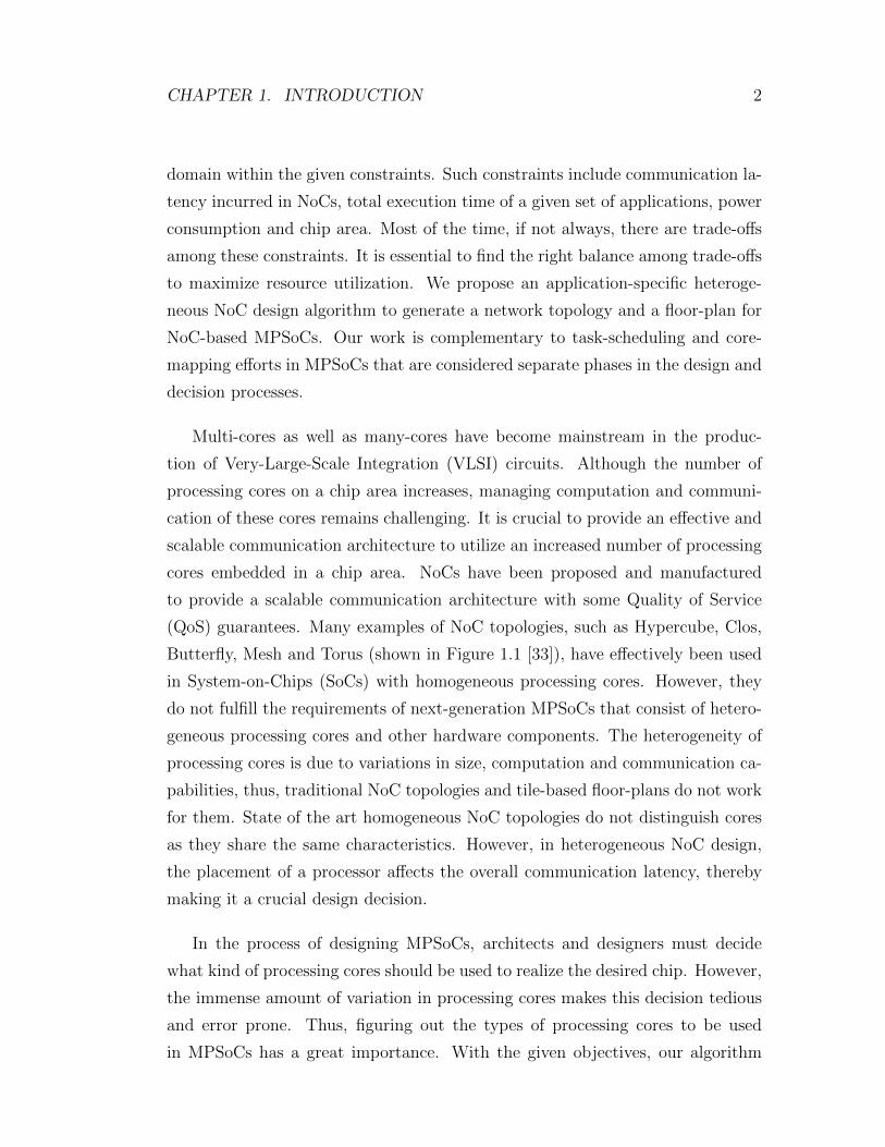
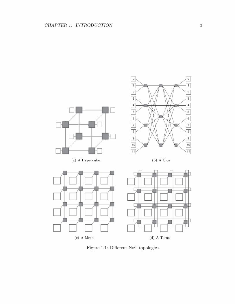
(QoS) guarantees. Many examples of NoC topologies, such as Hypercube, Clos,
Butterfly, Mesh and Torus (shown in Figure 1.1 [33]), have effectively been used
in System-on-Chips (SoCs) with homogeneous processing cores. However, they
do not fulfill the requirements of next-generation MPSoCs that consist of hetero-
geneous processing cores and other hardware components. The heterogeneity of
processing cores is due to variations in size, computation and communication ca-
pabilities, thus, traditional NoC topologies and tile-based floor-plans do not work
for them. State of the art homogeneous NoC topologies do not distinguish cores
as they share the same characteristics. However, in heterogeneous NoC design,
the placement of a processor affects the overall communication latency, thereby
making it a crucial design decision.
In the process of designing MPSoCs, architects and designers must decide
what kind of processing cores should be used to realize the desired chip. However,
the immense amount of variation in processing cores makes this decision tedious
and error prone. Thus, figuring out the types of processing cores to be used
in MPSoCs has a great importance. With the given objectives, our algorithm
CHAPTER 1. INTRODUCTION 3
(a) A Hypercube (b) A Clos
(c) A Mesh (d) A Torus
Figure 1.1: Different NoC topologies.
CHAPTER 1. INTRODUCTION 4
identifies the processing cores that can be used in MPSoCs and places them on a
given chip area in a way that the total latency occurring on the chip is minimized,
while the given area is utilized as much as possible. It should be noted that the
regular NoC topologies are inappropriate for such cases because MPSoCs have
non-uniform sets of processing cores. Thus, an effective custom NoC is the key
to achieving the desired performance of an MPSoC.
1.2 Research Objectives
Application-specific NoC design is necessary to fulfill the requirements of the de-
sired MPSoC with the given constraints and available budget. One important
constraint is the communication latency that occurs among communicating pro-
cessing cores; our focus is on an NoC design that minimizes this communication
latency while still considering other constraints. In our implementation, commu-
nication latency is simply defined as the total time observed among processors
that are communicating due to the tasks assigned to them. We introduce an
application-specific communication latency-aware heterogeneous NoC design al-
gorithm that considers the given constraints and generates a floor-plan for the
desired MPSoC. Our approach takes a directed and acyclic task graph, a con-
strained chip area, and a set of processing core types as an input. Then it
produces an application-specific heterogeneous NoC design based on the given
tasks. Our heterogeneous NoC design algorithm has two objectives:
• to select appropriate processing cores from the available processor pool that
will be used in heterogeneous NoC, and
• to place selected processing cores on a given chip area.
These objectives are to be attained in such a way that the total execution of the
overall application is minimized.
To achieve these objectives, 2 strategies are proposed:

CHAPTER 1. INTRODUCTION 5
• biologically inspired evolutionary computational approach (a Genetic Algo-
rithm), and
• 2D Bin Packing.
First of all, we solve the mapping and selection problem using a Genetic Al-
gorithm. In the Genetic Algorithm, there are 5 important phases. These are
initialization, selection, crossover, mutation, and termination which will be ex-
plained in detail in Section 3.1.1. To apply Genetic Algorithm phases, we need a
population which consists of individuals. A typical NoC placement is called an
individual in our implementation. A collection of individuals indicate the final
selection and mapping of the processors into the given chip area. Since the ini-
tialization step of the Genetic Algorithm suffers from packing procedure, we used
2D Bin Packing Algorithm to solve the same problem. In 2D Bin Packing Algo-
rithm, we are given a rectangular area and a set of n rectangular items having
different dimensions and these rectangles are packed into the given area without
overlapping. The main objective of the 2D Bin Packing Algorithm is utilizing
the given area while our main concern is minimizing the communication latency.
Therefore, we converted this algorithm into our problem domain. Since the lay-
out that is found by 2D Bin Packing Algorithm is prone to end up with a local
optimum layout, we enhanced this algorithm by simulated annealing technique.
With this modified algorithm, our goal is to reach the global optimum result. The
details of the 2D Bin Packing Algorithm is given in Section 3.2. These strategies
are the first ones, to our knowledge, that explore the application-specific layout
which considers both the minimum communication latency and the chip area
utilization.
Along with generation of custom NoC topology, there are two other impor-
tant concerns that affect the overall performance of MPSoC: task scheduling and
core mapping. Basically, task scheduling is to identify the processing core that
will run the given task. Core mapping, on the other hand, is to place a given
processing core on a given NoC. There are various studies of task scheduling and
core mapping, such as A3MAP [20] and NMAP [35], in which the authors con-
sider the NoC to be fixed and given beforehand. Our work is complementary to
CHAPTER 1. INTRODUCTION 6
task scheduling and core mapping because their effectiveness is tightly coupled
to the NoC that is being used. Our algorithm cooperates with task-scheduling
and core-mapping algorithms during the generation of the desired NoC and the
floor-plan for the MPSoC. Our implementation shows that multiple constraints
must be considered simultaneously, even though they belong to separate stages
of the MPSoC design process.
1.3 Overview of the Thesis
The thesis is organized as follows:
• Chapter 2 gives the Related Work in the NoC and MPSoC domain.
• Chapter 3 examines the methodologies that we have used, namely Genetic
Algorithm and 2D Bin Packing Algorithm.
• Chapter 4 concludes and gives the future work on voltage island based
implementations.
• A set of sample layouts, the details of the benchmarks used in experimental
results, and the major components of the implementation are given in the
Appendix.
Chapter 2
Related Work
MPSoCs [31, 32] has become popular due to its promising architecture combin-
ing different types of processing cores, networking elements, memory components
and other hardware subsystems on a single chip. One of the major distinctions
of MPSoC technology is its communication architecture. In distributed multi-
processors, communication between the processing cores is performed through
traditional networking components such as Ethernet, which although provides
high bandwidth, may suffer from high latency for critical applications. On the
other hand, the processing cores communicate through bus, crossbar and/or NoC
technologies [21, 36, 24] in MPSoCs that provide lower latency compared to Eth-
ernet. Among the communication types used in MPSoCs, NoC seems the only
solution for very large scale MPSoC designs.
The main concerns in designing NOCs include power consumption, perfor-
mance, area, bandwidth, latency, throughput, and wire length. Cong et al. [8] de-
velop an algorithm that minimizes the dead area on the chip. Ye and Micheli [50]
try to minimize the wire length of resulting NoCs. Ching et al. [7] and
Lee et al. [27] minimize the power consumption by voltage island generation
technique. Ching et al. [7] propose an algorithm where they try to partition a
given m x n grid into a set of regions while decreasing the total number of regions
as much as possible. They use a threshold which is based on the fact that the
voltage assigned to a cell should not be lower than the required voltage. There
7

CHAPTER 2. RELATED WORK 8
is a similar survey done by Hu et al. [18] where authors first partition the given
area into a set of voltage islands and cores, followed by area-planning and floor-
planning. Their objective is to simultaneously minimize power consumption and
area overhead, while keeping the number of voltage islands less than or equal to
a designer-specified threshold. Lee et al. [27] present an algorithm where they
apply a dynamic programming based approach to assign the voltage levels. Ma
and Young [30] propose an algorithm which is similar to [27]. They partition
a given area into a set of voltage islands with the aim of power saving. Their
floor-planner algorithm can be extended to minimize the number of level shifters
between different voltage islands and to simplify the power routing step.
Kim and Kim [23] try to find a balance between the area utilization and
total wire length. There exist commercial and non-commercial tools for NoC
design. One of them is Versatile Place and Route (VPR) [3], which is a packing,
placement and routing tool that minimizes the routing area. Kakoee et al. [22]
develop another tool that is claimed to be more interactive. A survey on NoC
design was conducted by Murali et al. [34] who also design an application-specific
NoC with floor-plan information. Their main concern is the wiring complexity
of the NoC during the topology generation procedure. Murali and Micheli [35]
present a fast algorithm called NMAP for core mapping into mesh-based NoC
topology while minimizing the average communication delay. For custom NoCs
and irregular mesh, a core graph, which describes the communication among dif-
ferent cores, is needed for floor-planning. Min-cut partitioning on the task graph
is explored by Leary et al. [26], who produce a floor-planning-aware core graph.
Jang and Pan [20] propose an architecture-aware analytic mapping algorithm
called A3MAP for both min-cut partitioning and mapping with homogeneous
cores and heterogeneous cores. Hu et al. [19] propose a method for minimizing
latency and decreasing power consumption.
An Integer Linear Programming (ILP)-based approach is introduced in [42] to
minimize the total energy consumption of NoCs. Banerjee et al. [2] follow a similar
approach and propose a Very High Speed Integrated Circuit Hardware Descrip-
tion Language (VHDL)-based cycle-accurate register transfer level model. They
considered the trade-off between power and performance. Srinivasan et al. [44]
CHAPTER 2. RELATED WORK 9
present a survey on these approaches considering performance and power require-
ments. Another concern is the minimization of execution time of the placement
algorithms with the help of ILP [37]. Srinivasan and Chatha [43] propose another
ILP-based approach that takes throughput constraints into account.
Heterogeneous chip multiprocessor design requires the placement of different
types of processors in a given chip area that resembles a 2D Bin Packing problem
with additional constraints such as latency. The placement problem can be sep-
arated into two: global and detailed placement. Detailed placement was studied
by Pan et al. [39]. Hdjiconstaninusu and Iori [15] present a heuristic approach
for solving 2D single large object placement problem, called 2SLOPP.
Hybrid genetic algorithms for the rectangular packing problem are presented
by Schnenke and Vornberger [41]. They target various problems such as con-
strained placement, facility layout problems and generation of VLSI macro cell
layouts. Terashima-Marın et al. [46] introduce a hyper-heuristic algorithm and
classifier systems for solving 2D regular cutting stock problems. Pal [38] compares
three heuristic algorithms for the cutting problem. He compares the performance
of the algorithms based on the wasted area. In addition to heuristic algorithms,
optimal rectangle placement algorithms have been proposed for certain special
cases. Healy and Creavin [16] propose an algorithm that has O(NlogN) time.
They try to solve the problem of placing a rectangle in a 2D space that may
not have the bottom left placement property. Cui [10] studies a recursive algo-
rithm for generating two-staged cutting patterns of punched strips. Lauther [25]
introduces a different placement algorithm for general cell assemblies, using a
combination of the polar graph representation and min-cut placement. Wong et
al. [47] develop a similar algorithm that employs simulated annealing and that
tries to minimize the total area and wire length simultaneously. Cong et al. [9]
compare a set of rectangle packing algorithms to observe area-optimal packing.
They minimized the maximum block aspect ratio subject to a zero-dead-space
constraint. There are different types of packing algorithms, namely Parquet [1],
B*-tree [6], TCG-S [28] and BloBB [5] that Cong et al. used to compare the
area-optimality of their algorithm. We also compare our algorithm with these
algorithms.

CHAPTER 2. RELATED WORK 10
Wei et al. [48] deal with the 2D rectangular packing problem, also called
the rectangular knapsack problem, which aims to maximize filling rate. They
divide the problem into two stages: first they present a least-wasted strategy
that evaluate the positions of rectangles, and then conduct a random local search
to improve the results. The latency-aware NoC design algorithm that we present
in this paper is based on their work. The details are given in Section 3.2.2.
Chapter 3
Methodologies
3.1 Heuristic Algorithm
As a first methodology, we use a biologically-inspired evolutionary (genetic) al-
gorithm, that places processing cores on a given chip area while satisfying the
communication latency constraints. Genetic Algorithm is selected because it
solves problems relatively in a short time and generates reasonable templates to
cover all features of a problem.
Our goal is to minimize the maximum execution latency among heterogeneous
CMPs on NoC by finding optimal layout within a given chip area budget in a
reasonable amount of time. We propose an approach to generate NoC architec-
ture that includes hundreds to thousands of heterogeneous processors by using a
heuristic algorithm. By the help of Genetic Algorithm;
• We minimize the communication latency, which includes communication
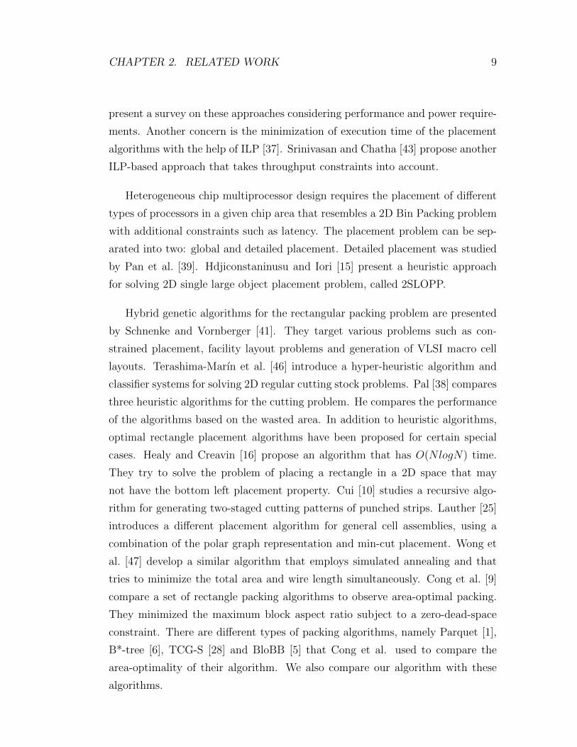
and computational costs. Figure 3.1 illustrates two heterogeneous NoC
designs obtained using the proposed approach. In Figure 3.1 (a), a het-
erogeneous NoC layout is generated with the order of P2, P1, P2, P3 and
in Figure 3.1 (b), the places of the processors are changed. There are four
11
CHAPTER 3. METHODOLOGIES 12
(a) First heterogeneous NoC layout. (b) Second heterogeneous NoC layout.
Figure 3.1: The algorithm for exploring a latency-aware NoC topology and pro-cessing core placement.
tasks and they are mapped one-to-one to the processors. Maximum commu-
nication latency for the first layout is greater than the second heterogeneous
NoC layout. Therefore, we select the second layout. We aim to minimize
the maximum latencies by remapping processors on chip without changing
tasks.
• We reduce the execution time significantly.
• The proposed approach provides an infrastructure for multi-functional de-
vices [45].
3.1.1 Implementation Details of Genetic Algorithm
The Genetic Algorithm is a search technique that is used to find optimal or
approximate solutions to the given problem set. It is a kind of evolutionary algo-
rithm that is inspired from crossover of chromosomes. It uses the initialization,
mutation, selection and crossover phases. At the beginning of the algorithm, there
should be a population that consists of individuals. These individuals come into
existence with the various combinations of chromosomes. During the life time,
these chromosomes are exposed to mutation. As a result of the mutation, some
individuals are enhanced but some of them are deteriorated. These individuals
CHAPTER 3. METHODOLOGIES 13
are selected according to a spontaneous selection rule. Not only mutation but
also crossover is applied to individuals and same procedure is followed.
In our case, more durable individuals correspond to heterogeneous NoC ar-
chitecture designs are generated with minimum communication latency. For ex-
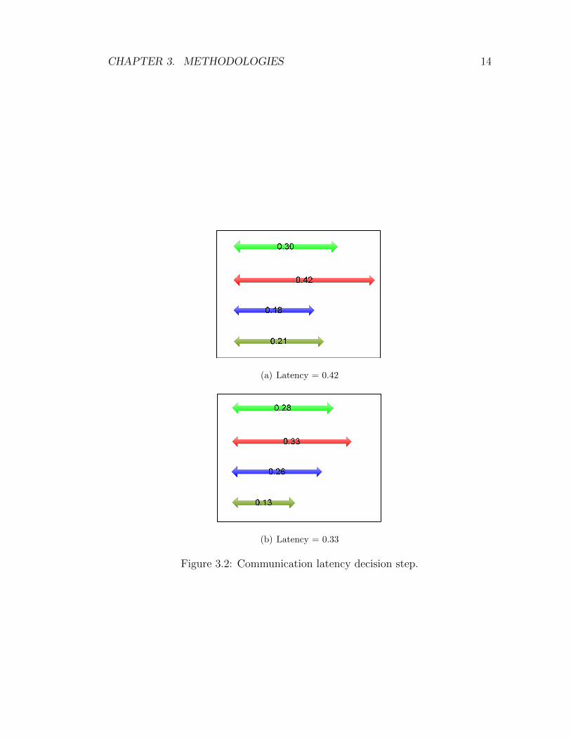
ample, in Figure 3.2, tasks are scheduled to the heterogeneous processors and the
second task takes the longest time to finish, which is 0.42 seconds. The arcs indi-
cate the execution time of the given task on the mapped processor. This schedule
is derived from the individuals shown in Figure 3.1. Then, a new mapping is gen-
erated according to the Genetic Algorithm rules. The new communication latency
is calculated for the task that requires the longest time to finish. If the commu-
nication latency of the newly generated placement is less than the previous one,
then we select this placement, which is called the individual. We replace the indi-
viduals whose communication latencies are higher in the population with the new
individual. It is shown that new communication latency is 0.33 seconds, which is
less than the first one; thus, it is selected.
The Genetic Algorithm is composed of 5 important stages: initialization,
selection, crossover, mutation, and termination.
3.1.1.1 Initialization
At the beginning of the Genetic Algorithm, a population that consists of ran-
domly generated individuals is needed. The number of individuals should
be determined intelligently because if it is not selected correctly, the pro-
cessing takes longer than the brute force approach. In our experiments,
the individuals are represented by the sequence of processors that are as-
signed to the nodes. Each appropriate chip design is called an individ-
ual. A typical individual has a sequence of processors in the format
<Type of processor, height, width, x-coordinate, y-coordinate>. For
example, in Figure 3.3 (a), there are three types of processors 1, 2, and
3. In Figure 3.3 (b), four different tasks are assigned to four proces-
sors which is called an individual. The representation of an individual is
CHAPTER 3. METHODOLOGIES 14
(a) Latency = 0.42
(b) Latency = 0.33
Figure 3.2: Communication latency decision step.

CHAPTER 3. METHODOLOGIES 15
(a) Types of processors. (b) A sample heterogeneous NoC.
Figure 3.3: Initialization step of the Genetic Algorithm.
(2, 2, 3, 0, 0) ⇒ (1, 1, 1, 3, 0) ⇒ (2, 3, 2, 4, 0) ⇒ (3, 3, 3, 0, 2).
The type of the processor is randomly selected and checked whether it fits
into the chip area. Algorithm 1 gives the pseudo-code of the initialization step.
Algorithm 1 Initialization
1: function initialization(Cx, Cy, placedArea,N)
2: CPU ⇒ select randomly
3: if isFit(CPU , placedArea) then
4: placeCPU(CPU , placedArea)
5: initialization(Cx, Cy, placedArea ∪ CPU , N -1)
6: else
7: initialization(Cx, Cy, placedArea, N)
8: end if
In this stage, isFit() method takes a crucial role because selected processor is
sent to isFit() method and it checks point-by-point to determine whether it fits or
not. Therefore, to place the next processor into the current heterogeneous NoC
layout, we search for an available position starting from the origin all the way to
the top right corner of the chip. If we divide the chip area using a regular grid
and most of the area is packed, a newly selected processor will check cell-by-cell
in the regular grid, where there are even placed rectangles.
CHAPTER 3. METHODOLOGIES 16
3.1.1.2 Selection
After the initialization stage, a set of individuals are selected to generate a new
population. The individuals are selected according to their fitness rates, which is
a function of f(x).
f(x) = max
(Li/Ck +
T−1∑j=0
Distance(Pk, Pl)× Affin(Ti, Tj)
)(3.1)
In Equation 3.1, k= i mod N, l=j mod N with 0 ≤ i, j < T , 0 ≤ k, l < N , and
i 6= j, k 6= l, where T is the number of tasks and N is the number of processors.
Affin(Ti, Tj) is the affinity between the current tasks, which is derived from
TGFF [11] and the distance is calculated using the Manhattan distance function.
Li refers to the load of the ith task and Ck is the capacity of the assigned
processor. Similarly, Pk refers to the kth processor and Ti refers to the ith task. In
the equation, the distance between a particular processor and the other processors
and the affinity of a task on that processor with all other tasks contributes to the
communication cost while Li/Ck is the processing cost. Adding communication
cost to the processing cost gives us the overall design cost. Basically, f(x) function
gives us the maximum communication latency of a layout for a given set of tasks
and processors in the NoC. More specifically, it is the maximum communication
latency among individuals in the population. Since, our goal is to minimize the
maximum communication latency, we choose individuals that have smaller f(x)
values. It is assumed that the fitness values of their children will also be low. In
the experiments, we used the roulette wheel technique [14] to select individuals.
In the roulette wheel technique, each individual is given a slice of a circular area
according to the fitness rate, and then the individuals whose slices are larger are
selected. In the experiments, the total cost of each design is calculated and a
fitness rate is assigned to each individual according to its communication latency.
The individuals that have high latency are selected and the crossover operation
is applied to these individuals in order to minimize the maximum latency.
CHAPTER 3. METHODOLOGIES 17
3.1.1.3 Crossover
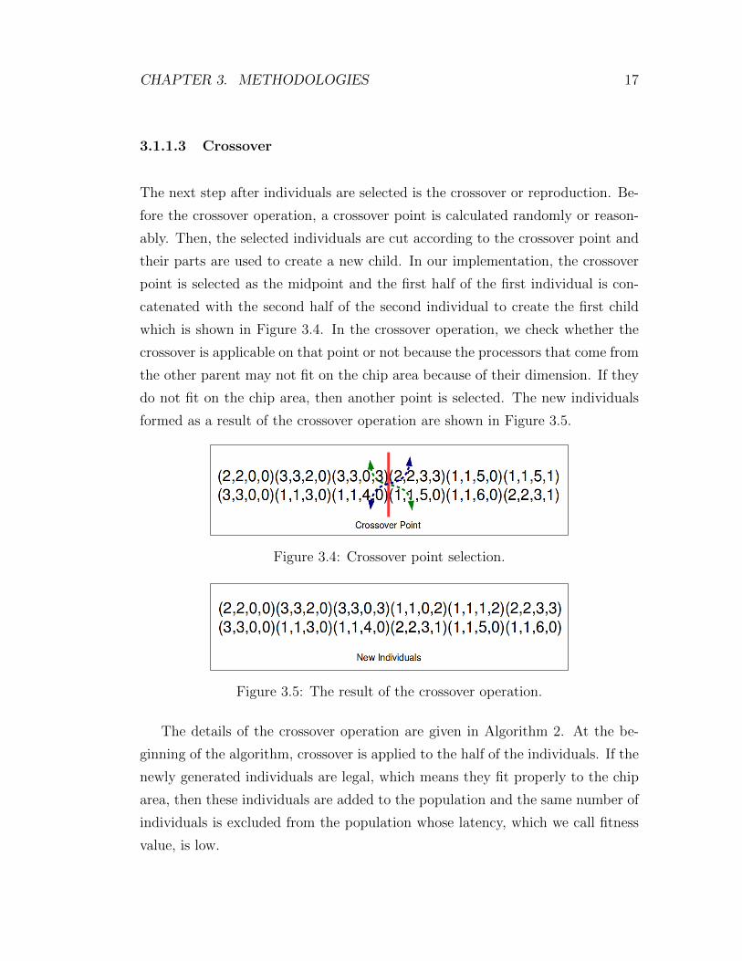
The next step after individuals are selected is the crossover or reproduction. Be-
fore the crossover operation, a crossover point is calculated randomly or reason-
ably. Then, the selected individuals are cut according to the crossover point and
their parts are used to create a new child. In our implementation, the crossover
point is selected as the midpoint and the first half of the first individual is con-
catenated with the second half of the second individual to create the first child
which is shown in Figure 3.4. In the crossover operation, we check whether the
crossover is applicable on that point or not because the processors that come from
the other parent may not fit on the chip area because of their dimension. If they
do not fit on the chip area, then another point is selected. The new individuals
formed as a result of the crossover operation are shown in Figure 3.5.
Figure 3.4: Crossover point selection.
Figure 3.5: The result of the crossover operation.
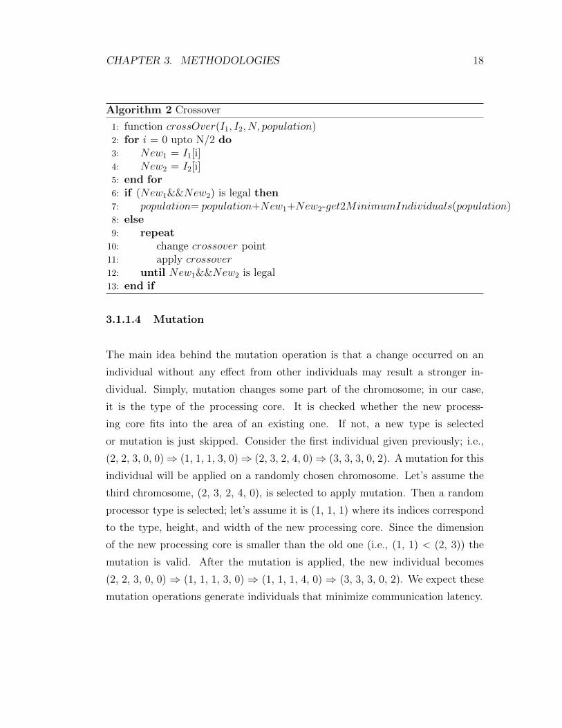
The details of the crossover operation are given in Algorithm 2. At the be-
ginning of the algorithm, crossover is applied to the half of the individuals. If the
newly generated individuals are legal, which means they fit properly to the chip
area, then these individuals are added to the population and the same number of
individuals is excluded from the population whose latency, which we call fitness
value, is low.
CHAPTER 3. METHODOLOGIES 18
Algorithm 2 Crossover
1: function crossOver(I1, I2, N, population)2: for i = 0 upto N/2 do3: New1 = I1[i]4: New2 = I2[i]5: end for6: if (New1&&New2) is legal then7: population= population+New1+New2-get2MinimumIndividuals(population)8: else9: repeat
10: change crossover point11: apply crossover12: until New1&&New2 is legal13: end if
3.1.1.4 Mutation
The main idea behind the mutation operation is that a change occurred on an
individual without any effect from other individuals may result a stronger in-
dividual. Simply, mutation changes some part of the chromosome; in our case,
it is the type of the processing core. It is checked whether the new process-
ing core fits into the area of an existing one. If not, a new type is selected
or mutation is just skipped. Consider the first individual given previously; i.e.,
(2, 2, 3, 0, 0)⇒ (1, 1, 1, 3, 0)⇒ (2, 3, 2, 4, 0)⇒ (3, 3, 3, 0, 2). A mutation for this
individual will be applied on a randomly chosen chromosome. Let’s assume the
third chromosome, (2, 3, 2, 4, 0), is selected to apply mutation. Then a random
processor type is selected; let’s assume it is (1, 1, 1) where its indices correspond
to the type, height, and width of the new processing core. Since the dimension
of the new processing core is smaller than the old one (i.e., (1, 1) < (2, 3)) the
mutation is valid. After the mutation is applied, the new individual becomes
(2, 2, 3, 0, 0)⇒ (1, 1, 1, 3, 0)⇒ (1, 1, 1, 4, 0)⇒ (3, 3, 3, 0, 2). We expect these
mutation operations generate individuals that minimize communication latency.

CHAPTER 3. METHODOLOGIES 19
3.1.1.5 Termination
These steps are repeated until a termination criterion is reached. The termination
criteria are as follows [17]:
• a solution may be generated that satisfies the minimum latency criteria,
• the total number of combinations are applied, or
• the allocated time and cost budget is reached.
Additionally, we also terminate the process if the crossover operation does not
generate different children.
CHAPTER 3. METHODOLOGIES 20
3.2 2D Bin Packing
In the initialization step of the Genetic Algorithm given in 3.1.1.1, we assumed
the chip is composed of a grid and packing is done grid by grid. To do this, we
search for appropriate places for the rectangles on the chip area starting from the
origin (0,0). We select the available position starting from the origin to the top
right corner of the chip. In our Genetic Algorithm, for each coordinate in the
grid, we check whether a processor fits or not. However this exhaustive search
becomes impractical with larger dimensions. To overcome the efficiency problems
of this approach we implemented a 2D Bin Packing Algorithm.
In the two-dimensional bin packing problem, we are given a rectangular area,
having width W and height H, and a set of n rectangular items with width
wj ≤ W and height hj ≤ H, for 1 ≤ j≤ n. These rectangles are not identical
they have different properties. The problem is to pack these rectangles into a
given area, without overlapping. The items can be rotated or not. According to
literature [29], there are four categorization of 2D Packing which are OG, RG,
OF, RF.
• OG: the items are oriented (O), i.e., they cannot be rotated, and guillotine
cutting (G) is required;
• RG: the items may be rotated by 90◦ (R) and guillotine cutting is required;
• OF: the items are oriented and cutting is free (F);
• RF: the items are oriented and cutting is free (F);
In our approach, we used 2D Bin Packing with RG which allows a 90◦ rotation
to achieve a better result compared to Genetic Algorithm.
CHAPTER 3. METHODOLOGIES 21
3.2.1 Problem Formulation and Basic Approach
Here, we formulate the application specific latency-aware layout problem. The
notation used is given in Table 3.1.
Table 3.1: The nomenclature for the communication latency calculation.
Notation Definition
ς Task Scheduling Type
τ Set of tasks where τ = t1, t2, t3, ... , tN
πi Set of parent tasks of task i where πi ⊆ τ
LT Communication Latency
Lswitch , Lwire Latency on switch and latency on wire, respectively
θi Finish time of task i
Ti,j Execution time of task i on processing core j
Tnl Total execution time for no-latency consideration
Pi,j Power consumption of task i on processing core j
Pswitch, Pwire Power consumption on switch and power consumption on wire, respectively
PTi,j Power consumption of sending bits from processing
core running task i to processing core running task j
pw Wire power per bit for unit length of wire
ps Switching power per bit
dw Wire delay per bit for unit length of wire
ds Switching delay per bit
dss Setup delay for switch
δi,j Distance between processing cores running tasks i and task j
vi,j Communication volume from task i to task j

CHAPTER 3. METHODOLOGIES 22
3.2.1.1 Basic Approach
Problem domain is explained in below;
Input
• A chip with dimensions CW and CH .
• A set of processing core types P , including the set of execution times for
each tasks, Ti,j for executing Ti on processor Pj and the power consumption
during this execution procedure, Pi,j.
• Maximum number of processing cores that can be used in the placement
process.
• A directed acyclic task graph G = (V,E), where V is the set of tasks and
E is the set of communication volumes between tasks. An example task
graph is shown in Figure 3.6.
Output
• Generate an application specific latency-aware heterogeneous NoC design.
This placement ensures that the cores are placed near to their optimal places
that minimizes the communication latency for the given tasks graph.
The way of packing processors into the chip area used is presented by Wei et
al. [48]. First of all, we are given a set of processor types and their respective
features which are shown in Table 3.2.
Table 3.2: Processor types having different dimensions.Type Height Width Capacity PowerP0 5 3 60 20P1 3 4 80 10P2 8 2 20 15

CHAPTER 3. METHODOLOGIES 23
Figure 3.6: Sample task graph representing TGFF task graphs.
First layout is generated indirectly by selecting first set of processors randomly,
then these processors are sorted according to their area and used in packing. The
number of a specific processor type is determined during the algorithm execution
time. After the first placement process, we calculate the communication latency
of the current layout according to some criteria which will be examined in more
detail in the following sections. For communication latency calculation, we use a
task graph which is depicted in Figure 3.6.
General structure of the algorithm is shown in Figure 3.8. In step 1, a set
of processor type is determined but how many times a processor will be used is
not given and selected randomly. In step 2, selected processors are placed into
the chip area according to 2D Bin Packing Algorithm. After the generation of
the first layout, task graph is created in step 3 and then mapped into the layout
according to task scheduling as shown in step 4. Then the communication latency
is calculated for that layout. In each iteration, these steps are repeated without
generating a new task graph and the minimum communication latency layout is
selected.
Since Wei et al. [48] find local optimal layout, we have improved their al-
gorithm for finding global optimal layout by the help of simulated annealing
technique. Our base algorithm, which is 2D Bin Packing is called Latency-Aware
CHAPTER 3. METHODOLOGIES 24
Least Wasted First (LA+LWF) and simulated annealing version is called Simu-
lated Annealing Least Wasted First (SA+LWF).
3.2.1.2 Problem Formulation
Given set of tasks are represented as a directed acyclic graph. The tasks on
the given task graph is represented as τ where τ = t1, t2, t3, . . . , tN , while the
execution time of task i for the specified scheduling scheme ς is represented as
Ti,j. For a task that is dependent on some other tasks, the finish time represented
as θi can be calculated as
θi = Ti,j + max ( θk + LTi,k)
where θk is the time to finish of task k that is a parent of task i, i.e., tk ⊆ πi. The
formula tells us that if a task is dependent on some other tasks, it can not start
until all the parents finish their execution and send required data to the current
task where LTk,irepresents the time required to transfer vk,i bits from processing
core that task k is running on the processing core that task i is running on. LTk,iis
referred as communication latency between task k and task i. The contributors to
communication latency are time spent on switching element to send vk,i bits and
time spent to sent vk,i bits on wire. This gives us the formula of communication
latency between cores as:
LTk,i= dss + ( ds vk,i ) + ( dw vk,i δk,i)
where δk,i is the distance between the processors that run tasks k and i. Af-
ter finding time to finish all tasks and associated communication latencies, the
total execution time of the task graph and total communication latency can be
calculated. Total execution time is:
Ttotal = max(θi),
CHAPTER 3. METHODOLOGIES 25
where i = 1, 2, 3, ..., N . On the other hand, total communication latency is:
LT = Ttotal − Tnl,
where
Tnl = max ( Ti,j + max ( θk ) ).
and θk is time to finish task k that is a parent of task i ∈ τ , i.e., tk ⊆ πi. Note
that while evaluating θk for Tnl, we consider all LTi,ks to be zero.
The calculation of the total communication latency is a little tricky if the
task graph involves tasks that have more than one parent. When a task has two
parents as shown in Figure 3.7, task T13 has to wait until both tasks T10 and
T12 finish their execution and pass their data to task T13. At the time 50 task
T12 finishes its execution and starts sending data to task T13. It takes 100 time
units to send all its data. On the other hand, task T10 finishes its execution at
time 100 and it takes 60 time units to send its data to task T13. Although the
communication latency between T12 and T13 is higher than the communication
latency between T10 and T13, the communication latency between T10 and T13
is added to the total communication latency. This is because task T13 would
have to wait task T10 to finish even it would take no time to receive data from
task T10. While task T13 is waiting for task T10 to finish, task T12 has already
sent half of its data to the task T13. Thus, we have to consider a communication
latency after both tasks T10 and T12 are finished. At time 100 both tasks T10
and T12 are finished and task T10 starts to send its data to tasks T13 while task
T12 has already sent half of its data to task T13. After then, it takes 60 time units
for task T10 to send its data and it takes 50 time units for task T12 to send its
remaining data to task T13. For this reason the communication latency occurred
between task T10 and T13 is selected and added to the total communication
latency.
When both tasks T10 and T12 are finished, it takes LT13,12 - (φ10 - φ12) time
for task T12 to send its remaining data, while it takes LT13,10 time for T10 to
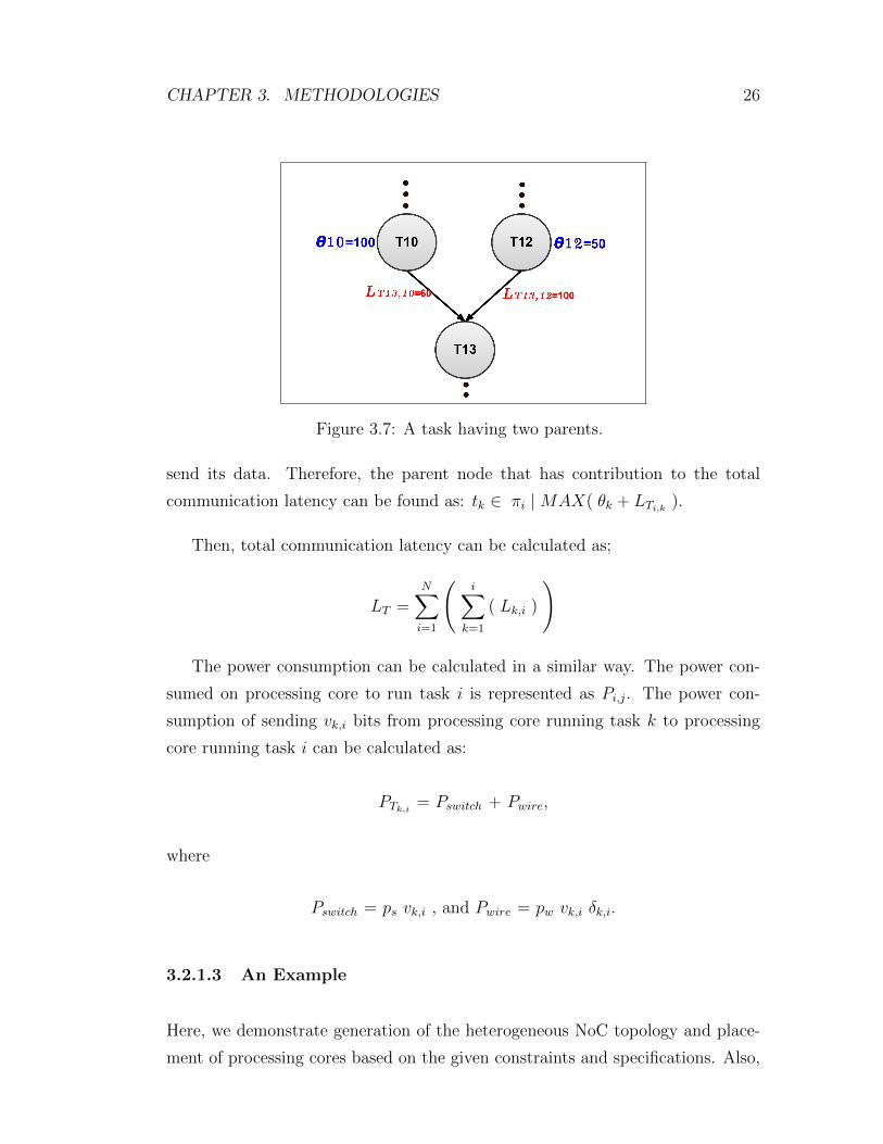
CHAPTER 3. METHODOLOGIES 26
Figure 3.7: A task having two parents.
send its data. Therefore, the parent node that has contribution to the total
communication latency can be found as: tk ∈ πi |MAX( θk + LTi,k).
Then, total communication latency can be calculated as;
LT =N∑i=1
(i∑
k=1
( Lk,i )
)
The power consumption can be calculated in a similar way. The power con-
sumed on processing core to run task i is represented as Pi,j. The power con-
sumption of sending vk,i bits from processing core running task k to processing
core running task i can be calculated as:
PTk,i= Pswitch + Pwire,
where
Pswitch = ps vk,i , and Pwire = pw vk,i δk,i.
3.2.1.3 An Example
Here, we demonstrate generation of the heterogeneous NoC topology and place-
ment of processing cores based on the given constraints and specifications. Also,

CHAPTER 3. METHODOLOGIES 27
Figure 3.8: The overview of the proposed approach.
we give a numerical example of how the total execution time and total communi-
cation latency are calculated based on the formulations given above. The overall
process is depicted in Figure 3.8.
At the beginning, the processing cores are selected and placed into
the chip area. In this example, the first layout consists of six cores,
(P0, 0, 0) → (P1, 0, 3) → (P1, 2, 3) → (P2, 2, 5) → (P2, 3, 5) → (P2, 4, 5)
where the parameters represent the processor type, x and y coordinates, respec-
tively. After the first layout is generated, the tasks given in the task graph are
assigned to the processing cores according to the scheduling scheme specified in
Section 3.2.2.4. In this example, the ordered scheduling is applied and we get
the layout shown in Figure 3.8. For this layout, we calculate total execution time
and communication latency. The total communication latency, LT is Ttotal − Tnl,and the total execution time is Ttotal = max(θi).
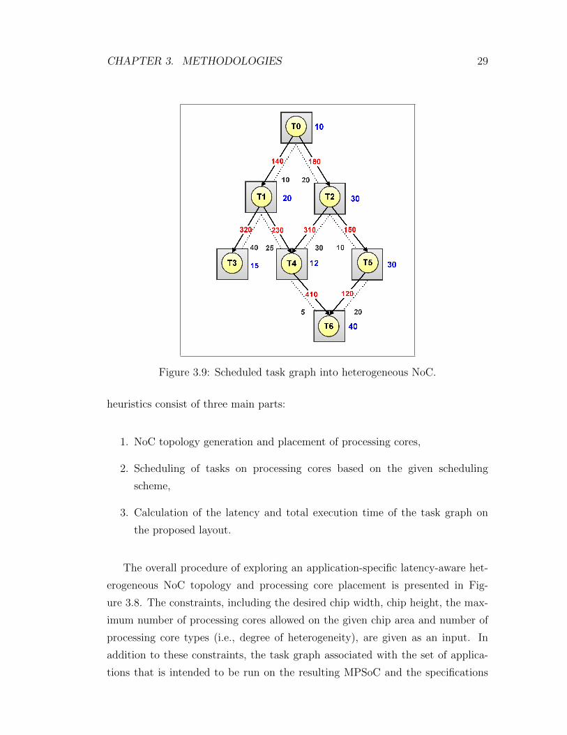
After the scheduling of tasks to the processing cores, we obtain a scheduled
task graph as illustrated in Figure 3.9. In this graph, the numbers next to the
outer circles represent the execution times for the tasks assigned to the particular
processing cores, i.e., Ti,j. The solid directed line represents the communication

CHAPTER 3. METHODOLOGIES 28
volume, i.e., vi,j, and the dashed line represents the distance between processing
cores, i.e., δi,j, that the corresponding tasks are assigned to.
The total execution time is 117.5 that is max(θi), where
θ0 = 10,
θ1 = 10 + [20 + (140× 10−3 × 10)] = 31.4,
θ2 = 10 + [30 + (180× 10−3 × 20)] = 43.6,
θ3 = 31.4 + [15 + (320× 10−3 × 40)] = 59.2,
θ4 = 12 + [max(31.4 + 5.75, 43.6 + 9.3)] = 64.9,
θ5 = 30 + [43.6 + (150× 10−3 × 10)] = 75.1
and
θ6 = 40 + [max(64.9 + 2.05, 75.1 + 2.4)] = 117.5.
Notice that we take dss and ds zero for simplicity and we consider all the wire
links are of the same type and dw as 10−3. After finding the total execution time,
the total communication latency can be calculated as follows:
LT = 117.5 - (10 + 30 + 30 + 40) = 7.5
3.2.2 2D Bin Packing Methodology
The communication latency occurring among communicating processing cores is
dominated by wire propagation delays. Intuitively, placing communicating pro-
cessing cores as close as possible will reduce this communication latency. Such a
placement might seem trivial for a couple of cores and tasks; however, it becomes
challenging when the number of processing cores and associated tasks scale up.
Finding optimal NoC topology and placement of a given set of processing cores
is known as an NP-hard problem [13]. In addition to the complexity of finding
proper placement for processing cores, the concerns of task scheduling and other
constraints such as power consumption make the problem even more challeng-
ing. Thus, we developed heuristics that effectively find near-optimal (i.e., satis-
fying the requirements) NoC topology and placement of processing cores within
a reasonable amount of time that fulfill the design requirements. Basically, our
CHAPTER 3. METHODOLOGIES 29
Figure 3.9: Scheduled task graph into heterogeneous NoC.
heuristics consist of three main parts:
1. NoC topology generation and placement of processing cores,
2. Scheduling of tasks on processing cores based on the given scheduling
scheme,
3. Calculation of the latency and total execution time of the task graph on
the proposed layout.
The overall procedure of exploring an application-specific latency-aware het-
erogeneous NoC topology and processing core placement is presented in Fig-
ure 3.8. The constraints, including the desired chip width, chip height, the max-
imum number of processing cores allowed on the given chip area and number of
processing core types (i.e., degree of heterogeneity), are given as an input. In
addition to these constraints, the task graph associated with the set of applica-
tions that is intended to be run on the resulting MPSoC and the specifications
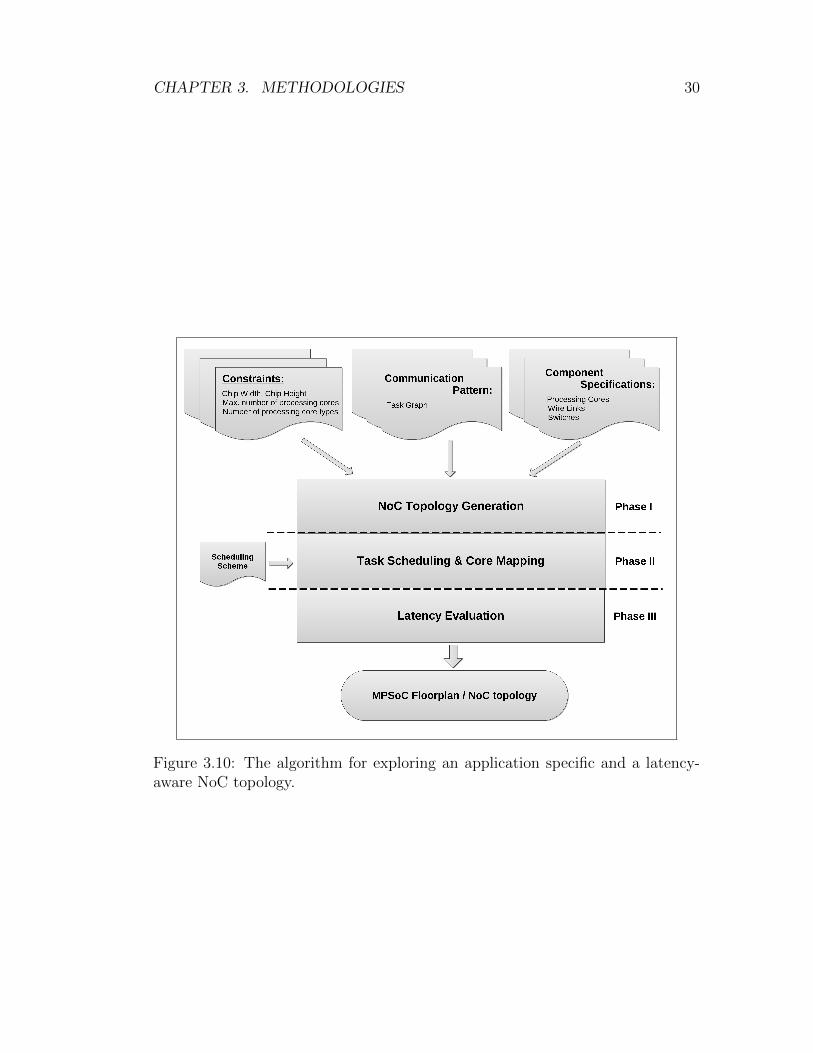
CHAPTER 3. METHODOLOGIES 30
Figure 3.10: The algorithm for exploring an application specific and a latency-aware NoC topology.
CHAPTER 3. METHODOLOGIES 31
of candidate processing cores as well as other subsystem components are also
given beforehand. Then, in the first phase, the algorithm evaluates the given
constraints and component specifications and generates a NoC topology and pro-
poses placement locations of the processing cores. In the second phase, the given
task graph is processed based on the specified scheduling scheme, and all tasks
are assigned to the processing cores that were determined in the first phase. In
the third phase, overall execution time of the task graph and associated commu-
nication latency are evaluated. These three phases are repeated until the desired
NoC topology and placement of processing cores are found, or the time specified
for the algorithm expires. At the end, the algorithm returns the NoC topology
and placement of processing cores, which minimizes the communication latency
for the given set of processing cores and tasks.
3.2.2.1 NoC Topology Generation
For simplicity, we consider that each processing core is associated with a unique
switch that is located at the bottom left corner of the core. Then, we generate
candidate topologies for selected processing cores by placing them on a given chip
area. Placement of processing cores on a chip area can be treated as a 2D Bin
Packing problem, thus, we extended and used the Least-Wasted-First (LWF) 2D
Bin Packing Algorithm presented by Wei et al. [48] to generate candidate NoC
topologies. In the LWF algorithm, a set of rectangles is selected and stored in
an array. The selection of the set of rectangles is repeated a certain number of
times. For each set of rectangles different placements are generated. To gener-
ate a placement, two rectangles are selected randomly from the array and then
swapped. If the new order of rectangles improves the area utilization, the new
order is accepted; otherwise, the old order is restored. This process is repeated a
certain number of iterations. Since the original LWF algorithm has an objective
function of area utilization, it eliminates placements that might minimize the la-
tency for the given set of processing cores and tasks. Thus, we modified the LWF
algorithm and made it latency-aware. Our modification is twofold:
• making the packing procedure latency-aware, and
CHAPTER 3. METHODOLOGIES 32
• improving efficiency of the algorithm by simulated annealing.
To make the placement latency aware, instead of looking at the area utiliza-
tion, we look at the latency for the given order. If the new order minimizes
the communication latency, then we accept the new order; otherwise we restore
the previous order. However, it is possible to be trapped into a local minimum
for the current order of processing cores. To overcome this and to improve the
efficiency of the algorithm, we further extended LWF and embedded simulated
annealing into it. If the new order of the processing cores does not minimize
the communication latency, we still accept the new order with some probabil-
ity, with the hope of escaping from local minima and reaching global minima.
The cooling schedule and acceptance probability function are dependent on the
given constraints and some other internal parameters of the algorithm. For the
sake of brevity, we do not examine the details of simulated annealing in here
but the implementation is given in Appendix C. We evaluate the base algorithm
and simulated annealing version in the experimental results section to show its
effect. While simulated annealing increases the probability of reaching optimal
heterogeneous NoC topology, or at least a better topology than that is gener-
ated by the base algorithm, it results with extra computation, which we consider
insignificant. Just before generating candidate placements as described above,
we must determine which processing cores will be used in the placement. To do
that, we pre-process the given constraints and component specifications. First,
we eliminate the processing cores that do not fit into the chip area. Then, we
select a number of processing cores as specified (i.e., the maximum number of
processing cores), ensuring that at least one processing core is selected from each
type of processing core. The selected processing cores are used in the algorithm.

CHAPTER 3. METHODOLOGIES 33
Algorithm 3 Heterogeneous NoC topology generation algorithm.
for i = 0 to maxSelect do
Fill processor list randomly from processor type list.
optimumLayout = Pack processor list into the chip area
minimumLatency = Calculate latency for optimumLayout
for j to maxSwap do
Select random a, b processors in processor list
Swap their position
currentLayout= Pack swapped processor list into the chip area
minimumLatency= Calculate latency for currentLayout
if currentLatency < minimumLatency then
optimumLayout = currentLayout
minimumLatency = currentLatency
end if
end for
end for
return optimumLayout
3.2.2.2 Packing Algorithm Details
2D Bin Packing Algorithm details are given in the following subsections.
3.2.2.3 Packing
We have divided packing procedure into 3 phases which is similar to Wei et
al. [48]. In their algorithm, initial rectangle set is given and they try to pack all
these rectangles at the same time. However, we are given only processor types,
so we select processors randomly at the beginning. Selection part is depicted in
Algorithm 4.

CHAPTER 3. METHODOLOGIES 34
Algorithm 4 Filling used processor list randomly from processor type list.
function selectPE()
while Used Processor List is not full do
Select Random PE()
Add Selected PE to Random PE List()
end while
After specifying used processor list, packing operation starts. First phase of
our algorithm is shown in Algorithm 5.
Algorithm 5 Packing algorithm details - Phase 1.
1: Generate Task List
2: Call Algorithm 4
3: 2D Packing
1: bestLayout = Algorithm 6(ProcessorList)
2: minimumLatency = CalculateLatency(bestLayout)
3: for i = 0 upto maxSelect do
4: newLayout = Algorithm 6(ProcessorList)
5: newLatency = CalculateLatency(newLayout)
6: if newLatency < minimumLatency then
7: select newly generated Layout
8: end if
9: Call Algorithm 4
10: end for
As it is explained in Algorithm 5, our algorithm starts by generating a task
graph. This task graph is generated only once and same task graph is used
during the execution time of the algorithm to obtain comparable results. After
task graph generation, processors are selected according to Algorithm 4. After the
initial settings, algorithm tries to find optimal layout which generates minimum
latency by the help of Phase 2 which is shown in Algorithm 6. In these algorithms,
maxSelect and maxSwap are the number of iterations which depend on the
processors that will be used in the packing.
CHAPTER 3. METHODOLOGIES 35
Algorithm 6 Packing algorithm details - Phase 2.
1: Sort the randomly generated processor list w.r.t their area
2: Swap wi and hi if wi is smaller than hi
3: for i = 0 upto ProcessorList do
4: Call Algorithm 7(Processor[i], bestLayout)
5: end for
6: minimumLatency=CalculateLatency(bestLayout)
7: for i = 0 upto maxSwap do
8: Select random a and b
9: Swap(SortedProcessorList, a, b)
10: newLayout = Algorithm 7(ProcessorList)
11: newLatency = CalculateLatency(newLayout)
12: if newLatency < minimumLatency then
13: select newly generated Layout
14: else
15: Swap(SortedProcessorList, a, b)
16: end if
17: end for
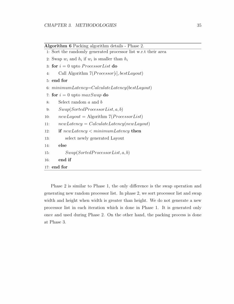
Phase 2 is similar to Phase 1, the only difference is the swap operation and
generating new random processor list. In phase 2, we sort processor list and swap
width and height when width is greater than height. We do not generate a new
processor list in each iteration which is done in Phase 1. It is generated only
once and used during Phase 2. On the other hand, the packing process is done
at Phase 3.

CHAPTER 3. METHODOLOGIES 36
Figure 3.11: Feasible points for the current heterogeneous NoC layout.
Algorithm 7 Packing algorithm details - Phase 3.
1: Sort packed processors w.r.t getX() plus getW (). If it ties sort w.r.t getY ()
plus getH()
2: Find feasible points similar to Martello et al. [29]
3: Calculate wasted area for the processor for each feasible point
4: If wasted areas tie then assign Goodness Number shown in Table 3.3 for those
points
5: Then select the smallest Goodness Number and pack that processor into that
feasible point
Packing procedure details are given in Algorithm 7. The way of finding feasible
points is taken from Martello et al. [29] and shown in Figure 3.11. For each feasible
point, we calculate the wasted area and if the wasted area is the same, then we
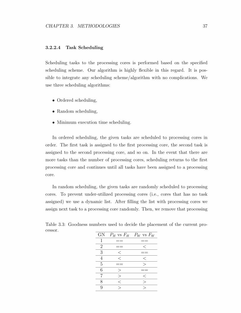
assign a Goodness Number shown in Table 3.3.
In Table 3.3, PH is the height of the current processor that we try to pack
and FH is the height of the current feasible point. For communication latency
calculation, we use task scheduling algorithms which is explained in the section
3.2.2.4.
CHAPTER 3. METHODOLOGIES 37
3.2.2.4 Task Scheduling
Scheduling tasks to the processing cores is performed based on the specified
scheduling scheme. Our algorithm is highly flexible in this regard. It is pos-
sible to integrate any scheduling scheme/algorithm with no complications. We
use three scheduling algorithms:
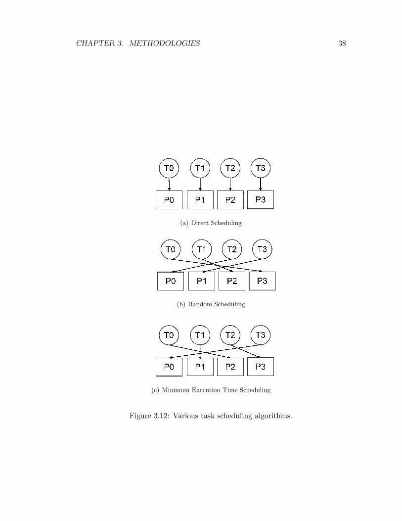
• Ordered scheduling,
• Random scheduling,
• Minimum execution time scheduling.
In ordered scheduling, the given tasks are scheduled to processing cores in
order. The first task is assigned to the first processing core, the second task is
assigned to the second processing core, and so on. In the event that there are
more tasks than the number of processing cores, scheduling returns to the first
processing core and continues until all tasks have been assigned to a processing
core.
In random scheduling, the given tasks are randomly scheduled to processing
cores. To prevent under-utilized processing cores (i.e., cores that has no task
assigned) we use a dynamic list. After filling the list with processing cores we
assign next task to a processing core randomly. Then, we remove that processing
Table 3.3: Goodness numbers used to decide the placement of the current pro-cessor.
GN PH vs FH PW vs FW
1 == ==2 == <3 < ==4 < <5 == >6 > ==7 > <8 < >9 > >
CHAPTER 3. METHODOLOGIES 38
(a) Direct Scheduling
(b) Random Scheduling
(c) Minimum Execution Time Scheduling
Figure 3.12: Various task scheduling algorithms.

CHAPTER 3. METHODOLOGIES 39
core from the list. If there are still unassigned tasks when the list is empty, we
fill the list again and proceed as described.
In minimum execution time scheduling, the given tasks are scheduled to pro-
cessing cores according to the execution times. Each task is assigned to a pro-
cessing core that will run the task faster than the others. Similar to random
scheduling, we use a dynamic list to prevent under-utilized and/or over-utilized
processing cores.
3.2.2.5 Latency Calculation
After all tasks are scheduled, we calculate the total communication latency and
execution time of the given task graph as described in section 3.2.1.
Chapter 4
Experimental Results
We implemented our application specific latency-aware heterogeneous NoC design
algorithm in Java, and performed the experiments in two different machines. The
first machine was an AMD PhenomII X6 1055T with 4GB of main memory on
a Linux kernel 2.6.35-24. The second machine was an Intel Pentium Dual-Core
E6500 with 2GB of main memory on a Linux kernel 2.6.35-28.
Experimental results consist of Genetic Algorithm and 2D Bin Packing Al-
gorithm results. Genetic Algorithm results are given first, followed by 2D Bin
Packing experimental results with two different categories. In the first category,
we aimed to show that the 2D Bin Packing Algorithm that we extended is compet-
itive with well-known packing algorithms. During these experiments we did not
consider the total execution time of the task graph and communication latency of
the generated NoC, but considered the packing efficiency in terms of dead areas
that could not be utilized for packing. For this category, we performed each set
of experiments 10 times and took the average. The Intel machine was used for
this category of experiments.
In the second category, we aimed to show that the application specific latency-
aware heterogeneous NoC design algorithm that is based on the extended LWF bin
packing algorithm generates heterogeneous NoC topology and places processing
cores on a given chip area such that the total execution time and communication
40
CHAPTER 4. EXPERIMENTAL RESULTS 41
latency of the given task graph are minimized considering the given constraints
and fulfill the requirements of the desired MPSoC. In this category, we performed
four sets of experiments for different benchmarks and settings. Again, we per-
formed each set of experiments 10 times and took the average. The AMD machine
was used for this category of experiments.
4.1 Experimental Results of Genetic Algorithm
We evaluated the given algorithm for the tasks that are generated by TGFF
software. We evaluated two random layouts in which tasks and processor types
are fixed (i.e., Random1, and Random2). We have four sets of tasks with different
number of tasks in each set. We compared Genetic Algorithm with two different
Random Algorithms. In Random 1, processing elements are fixed and same
processors are used. Whereas in Random 2, tasks are fixed. We have fixed these
two parameters in order to make controlled experiment. Each set was tested 1000
times to get admissible results. We have used 4 different task graphs containing
8, 16, 50, and 100 tasks, respectively.
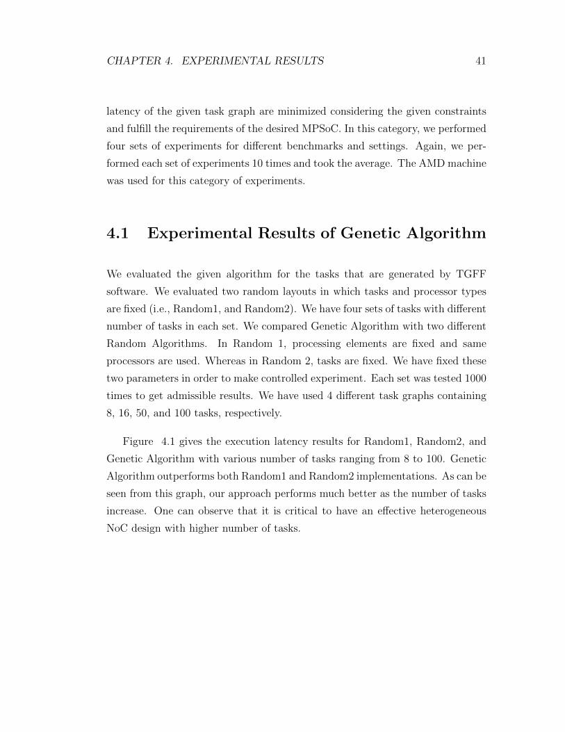
Figure 4.1 gives the execution latency results for Random1, Random2, and
Genetic Algorithm with various number of tasks ranging from 8 to 100. Genetic
Algorithm outperforms both Random1 and Random2 implementations. As can be
seen from this graph, our approach performs much better as the number of tasks
increase. One can observe that it is critical to have an effective heterogeneous
NoC design with higher number of tasks.

CHAPTER 4. EXPERIMENTAL RESULTS 42
Figure 4.1: Latency comparison of Genetic Algorithm with random algorithms.
4.2 Experimental Results of 2D Bin Packing Al-
gorithm
4.2.1 Packing Efficiency
In this category of experiments, we showed that LWF bin packing algorithm
that we used is competitive with well known bin packing algorithms in terms of
both area utilization and execution time. We compared LWF with Parquet [1],
B∗− tree [6], TCG-S [28] and BloBB [5] algorithms. We used a benchmark called
Floor-planning Examples with Known Optimal Area (FEKO-A) [40] that is an
extended version of MNCN benchmarks [49]. The FEKOA consists of the circuits
that are shown in Table 4.1.
The performance of the LWF bin packing algorithm is very competitive, as
seen in Table 4.2.11. For the first three circuits LWF finds the optimal layout
(i.e., zero dead area), as BloBB does. For FEKOA4 and FEKOA5 it performs
1The experiments with LWF were run on a 2800 MHz 6-Core AMD Phenom II X6 processor,unlike the rest of the experiments
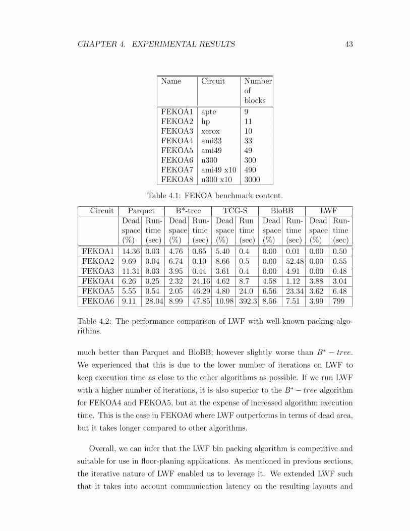
CHAPTER 4. EXPERIMENTAL RESULTS 43
Name Circuit Numberofblocks
FEKOA1 apte 9FEKOA2 hp 11FEKOA3 xerox 10FEKOA4 ami33 33FEKOA5 ami49 49FEKOA6 n300 300FEKOA7 ami49 x10 490FEKOA8 n300 x10 3000
Table 4.1: FEKOA benchmark content.
Circuit Parquet B*-tree TCG-S BloBB LWFDeadspace(%)
Run-time(sec)
Deadspace(%)
Run-time(sec)
Deadspace(%)
Runtime(sec)
Deadspace(%)
Run-time(sec)
Deadspace(%)
Run-time(sec)
FEKOA1 14.36 0.03 4.76 0.65 5.40 0.4 0.00 0.01 0.00 0.50FEKOA2 9.69 0.04 6.74 0.10 8.66 0.5 0.00 52.48 0.00 0.55FEKOA3 11.31 0.03 3.95 0.44 3.61 0.4 0.00 4.91 0.00 0.48FEKOA4 6.26 0.25 2.32 24.16 4.62 8.7 4.58 1.12 3.88 3.04FEKOA5 5.55 0.54 2.05 46.29 4.80 24.0 6.56 23.34 3.62 6.48FEKOA6 9.11 28.04 8.99 47.85 10.98 392.3 8.56 7.51 3.99 799
Table 4.2: The performance comparison of LWF with well-known packing algo-rithms.
much better than Parquet and BloBB; however slightly worse than B∗ − tree.
We experienced that this is due to the lower number of iterations on LWF to
keep execution time as close to the other algorithms as possible. If we run LWF
with a higher number of iterations, it is also superior to the B∗ − tree algorithm
for FEKOA4 and FEKOA5, but at the expense of increased algorithm execution
time. This is the case in FEKOA6 where LWF outperforms in terms of dead area,
but it takes longer compared to other algorithms.
Overall, we can infer that the LWF bin packing algorithm is competitive and
suitable for use in floor-planing applications. As mentioned in previous sections,
the iterative nature of LWF enabled us to leverage it. We extended LWF such
that it takes into account communication latency on the resulting layouts and

CHAPTER 4. EXPERIMENTAL RESULTS 44
proceeds accordingly in each iteration, leading to a heterogeneous NoC design
that minimizes total execution time and communication latency of the given task
graph.
4.2.2 Application-specific Latency-aware Heterogeneous
NoC Design
In this category of experiments, we show that the presented application-specific
latency-aware heterogeneous NoC design algorithm generates an NoC topology
and places the processing core on a given chip area such that total execution
time and communication latency are minimized for the given task graph. The
algorithm also considers the given constraints and fulfills the desired MPSoC
requirements. Considerations include keeping power consumption at acceptable
levels and increasing chip area utilization as much as possible.
We perform four sets of experiments in this category. In the first set, we show
that NoC designs that try to maximize chip area utilization without considering
latency as a first-class concern result in higher total execution time and commu-
nication latency. We compare our application-specific latency-aware NoC design
algorithm with CompaSS [4], which is known as a powerful packing algorithm for
NoC design. In this set of experiments, we use MCNC benchmarks with different
settings.
In the second set, we compare our application-specific latency-aware NoC
design algorithm with task scheduling and core-mapping algorithms. Such algo-
rithms consider that NoC is fixed and given beforehand. As we claim earlier,
to achieve the desired MPSoC, one must consider task scheduling, core map-
ping and NoC topology generation as a whole. We present a set of results here
to show that task-scheduling and core-mapping algorithms such as NMAP and
A3MAP do not minimize total execution time and communication latency since
they are oblivious to the NoC requirements of desired MPSoCs. We conceive that
our work is complementary to task-scheduling and core-mapping efforts such as
NMAP and A3MAP and will result in MPSoCs that minimize total execution
CHAPTER 4. EXPERIMENTAL RESULTS 45
time and communication latency. In this set of experiments, we use Embedded
System Synthesis Benchmarks Suite (E3S) [12] with different settings.
In E3S benchmarks, there are 45 different tasks and 17 different processors.
This benchmark suite contains task graphs for five embedded application types:
automotive/industrial, consumer, networking, office automation and telecommu-
nications. There is a version of each task graph for three kinds of systems:
distributed (cords), wireless client-server (cowls) and system-on-chip (mocsyn).
An application is described by a set of task graphs. The task types are shown in
Appendix B.1 and processor types are given in Appendix B.2. The task graphs
from E3S are directed acyclic graphs; they have a period and deadlines may be
set on tasks. The period of a task graph is defined as the amount of time between
the earliest start times of its consecutive executions. A deadline is defined as the
time by which the task associated with the node must complete its execution.
Each task graph is described using an ASCII file in the TGFF format.
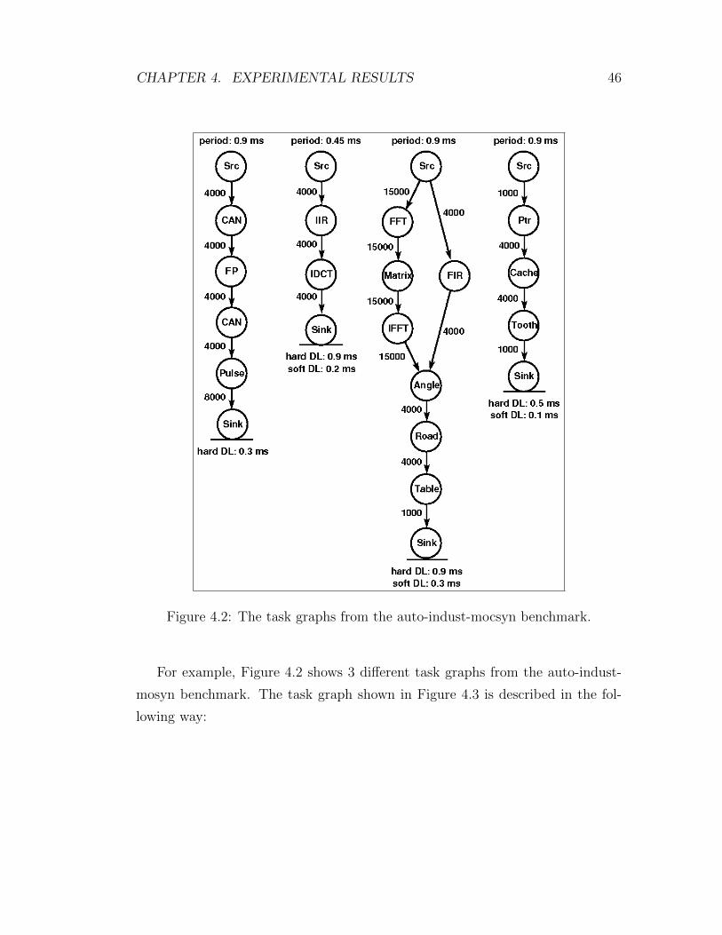
CHAPTER 4. EXPERIMENTAL RESULTS 46
Figure 4.2: The task graphs from the auto-indust-mocsyn benchmark.
For example, Figure 4.2 shows 3 different task graphs from the auto-indust-
mosyn benchmark. The task graph shown in Figure 4.3 is described in the fol-
lowing way:
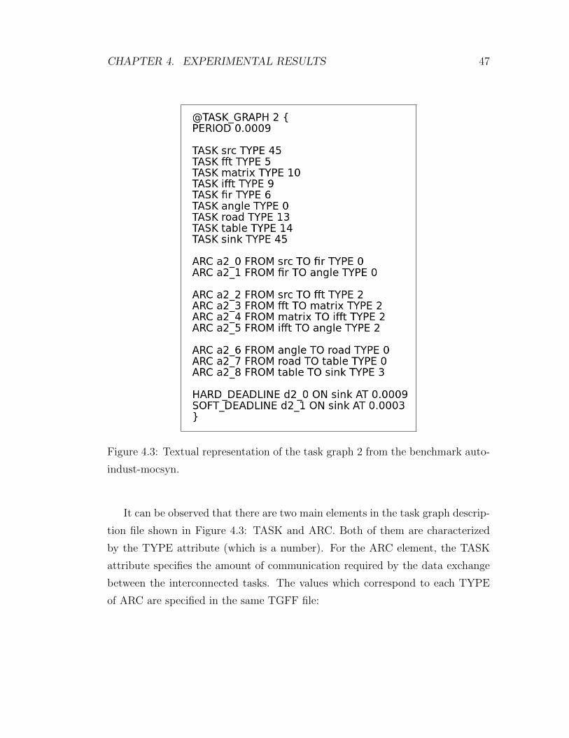
CHAPTER 4. EXPERIMENTAL RESULTS 47
Figure 4.3: Textual representation of the task graph 2 from the benchmark auto-
indust-mocsyn.
It can be observed that there are two main elements in the task graph descrip-
tion file shown in Figure 4.3: TASK and ARC. Both of them are characterized
by the TYPE attribute (which is a number). For the ARC element, the TASK
attribute specifies the amount of communication required by the data exchange
between the interconnected tasks. The values which correspond to each TYPE
of ARC are specified in the same TGFF file:

CHAPTER 4. EXPERIMENTAL RESULTS 48
Figure 4.4: The communication volumes in a TGFF task graph.
For example, TYPE 0 means a communication volume of 4000 bits. For the
TASK element, the TYPE attribute specifies the type of the task. For example,
TYPE 5 denotes a Fast Fourier Transform (Auto/Indust. Version). All these
types are described in Appendix B.1. For each type of task, performance indexes
are available. They were obtained using the embedded processors from Embedded
Microprocessor Benchmark Consortium (EEMBC) [12], which is a commercial
tool. Although there are 17 different processors, E3S used 34 processors because
E3S is based on the EEMBC benchmarks suite, so the writer of E3S benchmarks
could not reach the exact dimensions of the processors. The reason of giving
two different types for one processor is that. One of the processor type is set as
square, and the second one is a random rectangle.
In the third set of experiments, we use larger benchmarks for the scalability
analysis of our algorithm. We generate larger benchmarks that are based on E3S
benchmarks. In the larger benchmarks we use the same set of processing cores
and tasks as given in E3S; however, we extend the task graphs and replicated
tasks as well as processing cores accordingly.
In the fourth set of experiments, we generated fully-synthetic benchmarks to
extend the scalability analysis. We generated several benchmarks with a high
number of tasks and processing cores with TGFF. Figure 4.5 shows a task graph
generated by TGFF.

CHAPTER 4. EXPERIMENTAL RESULTS 49
Figure 4.5: Sample task graph generated by TGFF.
We use the delay and power models presented by Hu et al. [19] to calculate
communication latency and power consumption on switches and wires. The exe-
cution time of a given set of tasks and the power consumption of processing cores
are obtained from E3S benchmarks or generated through TGFF for this category
of experiments.

CHAPTER 4. EXPERIMENTAL RESULTS 50
4.2.2.1 Impact of Application-specific Latency-awareness
on Heterogeneous NoC Design
From now on, we refer the total execution time as communication latency for sim-
plicity. Note that under a certain scheduling scheme, minimizing total execution
time also means minimizing communication latency; thus we present the total
execution time in the figures given instead of separating total execution time and
communication latency.
As stated before, to have a desired MPSoC one must consider the total execu-
tion time and communication latency while generating heterogeneous NoC topol-
ogy in conjunction with other concerns. Figure 4.6 shows that our algorithm gen-
erates better NoC topologies that minimize latency for different task-scheduling
schemes than CompaSS does. Note that the simulated annealing version of the
algorithm performs better for ami33; however, it shows neither remarkable im-
provement nor degradation compared to the base algorithm for other benchmarks.
We think that this is acceptable, given the resulting average values (i.e., there
were tests where the simulated annealing version outperforms).
We use four different task graphs (tg1, tg2, tg4 and tg8) to evaluate the gen-
erated heterogeneous NoC topologies of CompaSS and the proposed algorithm.
In each task graph, there is a different number of tasks, depending on the circuit
of interest. For example, there are 8 × 49 tasks and 4 × 49 tasks for ami49 in
tg8 and tg4 respectively. Figure 4.7 shows the latency on NoCs generated by
CompaSS and our algorithms (both the base and simulated annealing versions)
for different task graphs. We present only apte, ami33 and ami49 here to keep
the figure readable. Minimum execution time scheduling is used in this setting.
4.2.2.2 Impact of Cooperation of NoC design with Task Scheduling
and Mapping
Figure 4.8 shows a normalized total execution time of E3S benchmarks for NMAP,
A3MAP and our algorithm. For NMAP and A3MAP a predefined custom NoC

CHAPTER 4. EXPERIMENTAL RESULTS 51
Figure 4.6: Comparison of CompaSS and presented algorithm on MCNC bench-marks.
Figure 4.7: Performance comparison for different task graphs.
CHAPTER 4. EXPERIMENTAL RESULTS 52
topology with seven processing cores was given. Since the NMAP and A3MAP
algorithms were constrained by the given NoC topology, they could not mini-
mize communication latency despite the best attempts with scheduling and core
mapping. On the other hand, our algorithm can effectively generate a NoC topol-
ogy that minimizes communication latency, although a simpler task-scheduling
scheme is used (i.e., minimum execution time scheduling) compared to NMAP
and A3MAP. Note that the simulated annealing version of the algorithm performs
better in consumer and telecom benchmarks while left behind the base algorithm
in auto-indust and networking benchmarks. This is due to the fact that the al-
gorithm is allowed to accept an order of processing cores with some probability
even if the order is not better than the previous one, as described in Section 3.2.2.
Such an accepted order may lead the algorithm to generate worse topologies as
well as better ones. Thus, to compensate for iterations performed on the wrong
order of processing cores, the number of iterations needs to be increased in the
simulated annealing version of the algorithm. Since we use the same number of
iterations for both the base and simulated annealing versions of the algorithm,
the decrease in performance of the simulated annealing version, shown in Fig-
ure 4.8 is acceptable. Performance can be improved with more iterations, which
will result in longer runs.
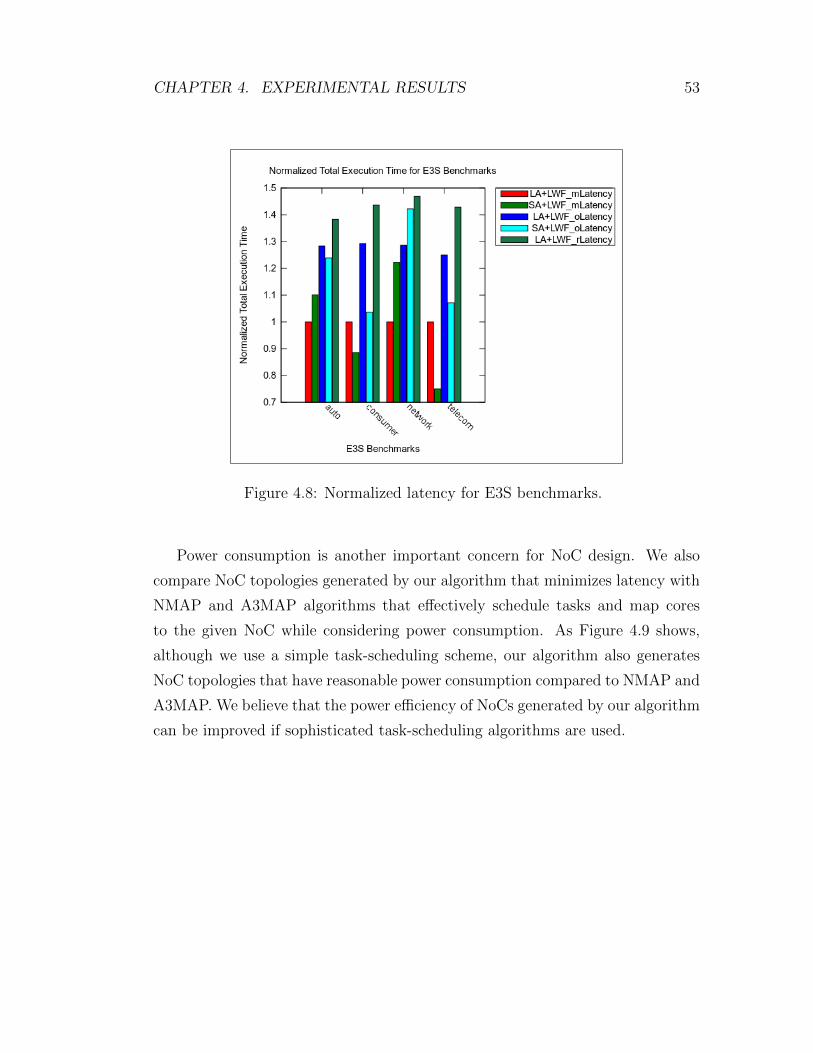
CHAPTER 4. EXPERIMENTAL RESULTS 53
Figure 4.8: Normalized latency for E3S benchmarks.
Power consumption is another important concern for NoC design. We also
compare NoC topologies generated by our algorithm that minimizes latency with
NMAP and A3MAP algorithms that effectively schedule tasks and map cores
to the given NoC while considering power consumption. As Figure 4.9 shows,
although we use a simple task-scheduling scheme, our algorithm also generates
NoC topologies that have reasonable power consumption compared to NMAP and
A3MAP. We believe that the power efficiency of NoCs generated by our algorithm
can be improved if sophisticated task-scheduling algorithms are used.
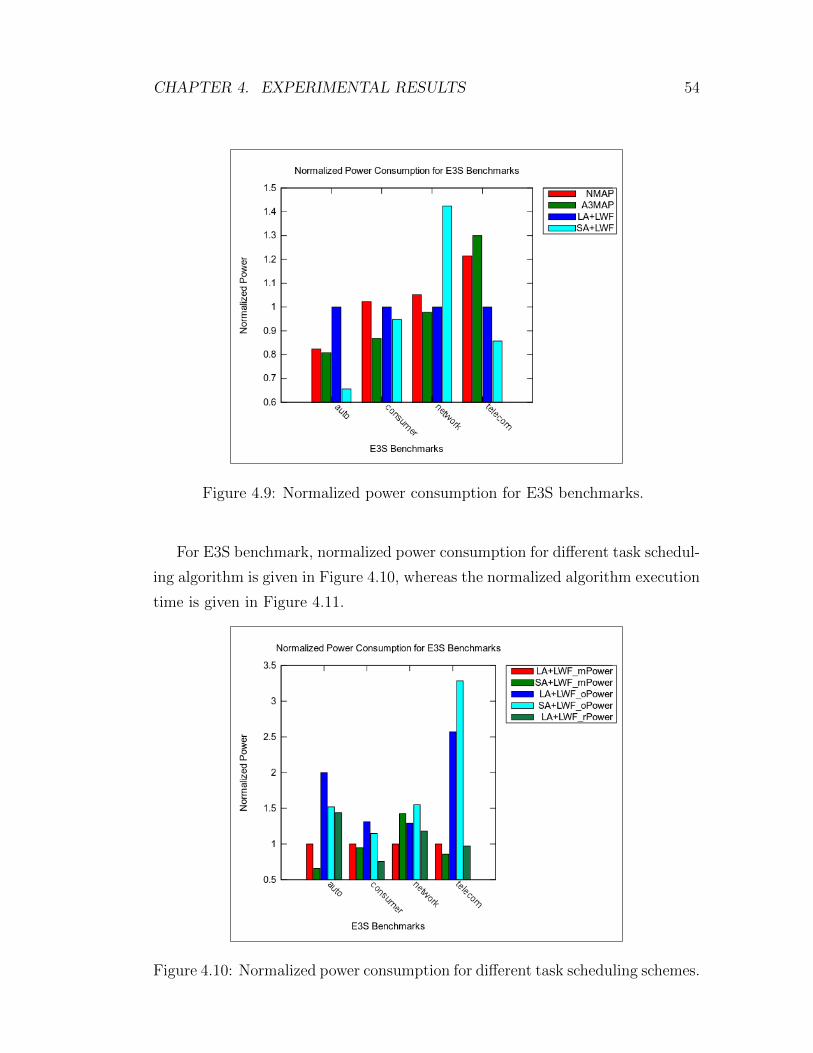
CHAPTER 4. EXPERIMENTAL RESULTS 54
Figure 4.9: Normalized power consumption for E3S benchmarks.
For E3S benchmark, normalized power consumption for different task schedul-
ing algorithm is given in Figure 4.10, whereas the normalized algorithm execution
time is given in Figure 4.11.
Figure 4.10: Normalized power consumption for different task scheduling schemes.
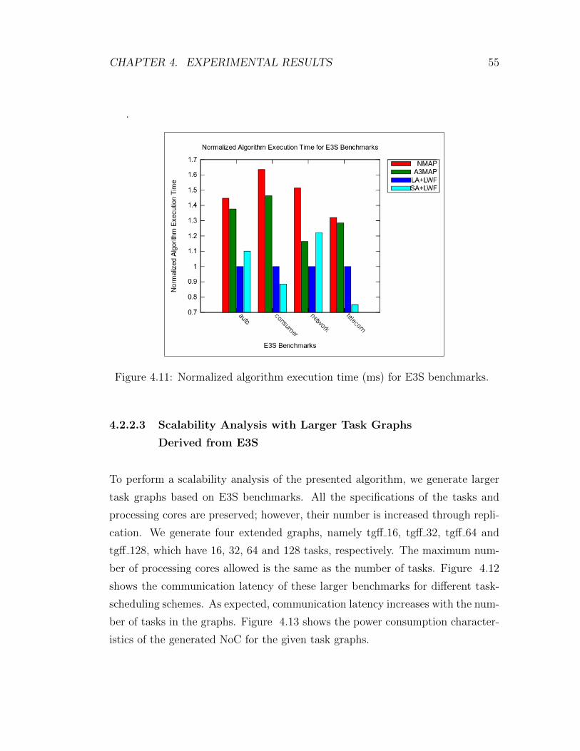
CHAPTER 4. EXPERIMENTAL RESULTS 55
.
Figure 4.11: Normalized algorithm execution time (ms) for E3S benchmarks.
4.2.2.3 Scalability Analysis with Larger Task Graphs
Derived from E3S
To perform a scalability analysis of the presented algorithm, we generate larger
task graphs based on E3S benchmarks. All the specifications of the tasks and
processing cores are preserved; however, their number is increased through repli-
cation. We generate four extended graphs, namely tgff 16, tgff 32, tgff 64 and
tgff 128, which have 16, 32, 64 and 128 tasks, respectively. The maximum num-
ber of processing cores allowed is the same as the number of tasks. Figure 4.12
shows the communication latency of these larger benchmarks for different task-
scheduling schemes. As expected, communication latency increases with the num-
ber of tasks in the graphs. Figure 4.13 shows the power consumption character-
istics of the generated NoC for the given task graphs.
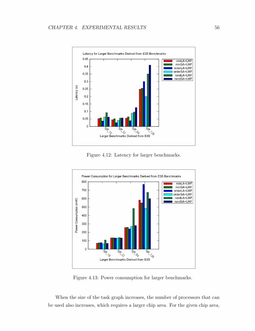
CHAPTER 4. EXPERIMENTAL RESULTS 56
Figure 4.12: Latency for larger benchmarks.
Figure 4.13: Power consumption for larger benchmarks.
When the size of the task graph increases, the number of processors that can
be used also increases, which requires a larger chip area. For the given chip area,

CHAPTER 4. EXPERIMENTAL RESULTS 57
the algorithm tries to best place processing cores as much as the number of tasks
(i.e., the ideal case is to assign one task per processing core); however, this may
not always be feasible due to the given chip area, specifications of processing cores
and other constraints. Figure 4.14 shows the number of processing cores placed
on a given chip area for different benchmarks and task scheduling schemes.
Figure 4.14: Number of processing cores placed on chip area.
4.2.2.4 Fully Synthetic on Latency-Aware
We extend our scalability analysis with fully synthetic task graphs and processing
cores for higher numbers. We generate two task graphs, one with 1024 and one
with 2048 tasks. We perform experiments with 256, 512 and 1024 processing
cores for the first graph, and 256, 512, 1024 and 2048 processing cores for the
second graph. Figure 4.15 show the latency versus the number of processing cores
available for 1024 and 2048 tasks with different scheduling schemes.
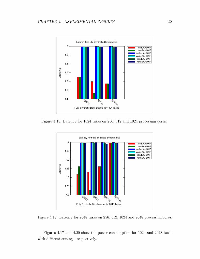
CHAPTER 4. EXPERIMENTAL RESULTS 58
Figure 4.15: Latency for 1024 tasks on 256, 512 and 1024 processing cores.
Figure 4.16: Latency for 2048 tasks on 256, 512, 1024 and 2048 processing cores.
Figures 4.17 and 4.20 show the power consumption for 1024 and 2048 tasks
with different settings, respectively.
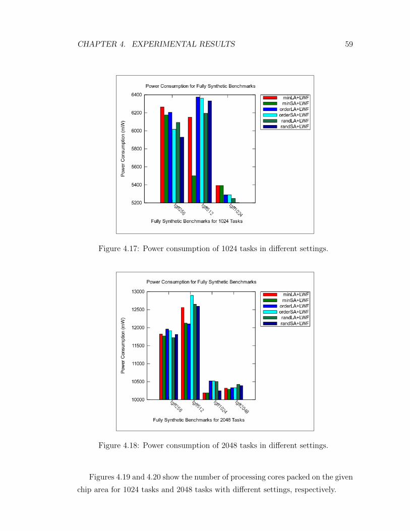
CHAPTER 4. EXPERIMENTAL RESULTS 59
Figure 4.17: Power consumption of 1024 tasks in different settings.
Figure 4.18: Power consumption of 2048 tasks in different settings.
Figures 4.19 and 4.20 show the number of processing cores packed on the given
chip area for 1024 tasks and 2048 tasks with different settings, respectively.
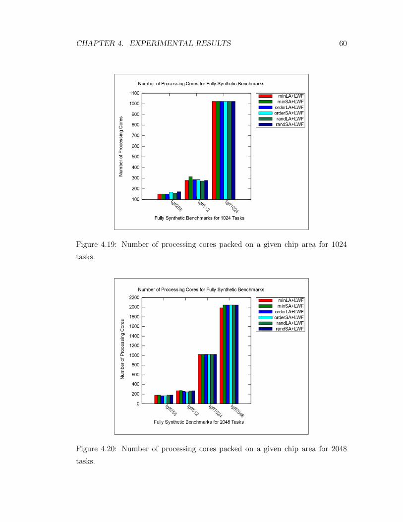
CHAPTER 4. EXPERIMENTAL RESULTS 60
Figure 4.19: Number of processing cores packed on a given chip area for 1024
tasks.
Figure 4.20: Number of processing cores packed on a given chip area for 2048
tasks.

CHAPTER 4. EXPERIMENTAL RESULTS 61
4.2.3 Task Scheduling Algorithm Analysis for MCNC
Benchmarks
There are three different types of task scheduling algorithms which are explained
in section 3.2.2.4. Their impacts are observed by MCNC benchmarks. The results
are given in the Figure 4.21, 4.22 and 4.23. In the Figure 4.21, minimum task
scheduling is examined.
Figure 4.21: Compass benchmark for Minimum Execution Time Scheduling
scheme.
It shows that minimum execution time scheduling algorithm gives the best
result. Ordered task scheduling algorithm gives latency degree between minimum
task scheduling algorithm and random task scheduling algorithm.

CHAPTER 4. EXPERIMENTAL RESULTS 62
Figure 4.22: Compass benchmark for Direct Scheduling scheme.
Figure 4.23: Compass benchmark for Random Scheduling scheme.
For these results, we have used tg8, which means the task graph which includes
maximum tasks. For ami33, tg8 means, we have 33 x 8 tasks. All of them are

CHAPTER 4. EXPERIMENTAL RESULTS 63
compared in Figure 4.24.
Figure 4.24: Overall task scheduling comparison for Compass benchmark.
4.2.4 Algorithm Intrinsics
This section describes the effects of internal parameters on the performance of the
algorithm. These parameters include maxSelect and maxSwap, as mentioned
in Section 3.2.2. Figure 4.25 shows the relationship between latency and the
maxSelect, maxSwap parameters that indicate the total number of iterations
the algorithm runs. The tuples given on the x-axis represent the maxSelect
and maxSwap parameters. As the number of iterations increases the latency
decreases for hp, ami33 and ami49. The latency remains the same for apte and
xerox when the number of iterations increases. This is because apte and xerox
have fewer number of processing cores and the algorithm completes the search
and finds the best NoC topology in fewer number of iterations; thus, increasing
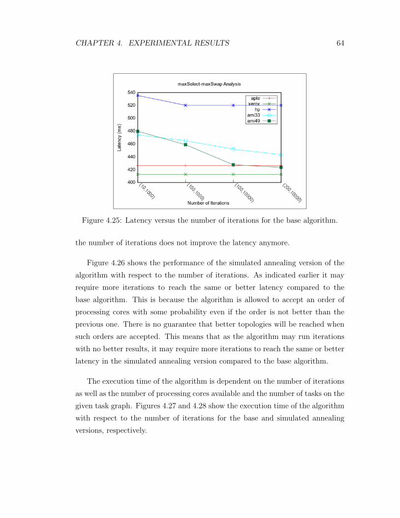
CHAPTER 4. EXPERIMENTAL RESULTS 64
Figure 4.25: Latency versus the number of iterations for the base algorithm.
the number of iterations does not improve the latency anymore.
Figure 4.26 shows the performance of the simulated annealing version of the
algorithm with respect to the number of iterations. As indicated earlier it may
require more iterations to reach the same or better latency compared to the
base algorithm. This is because the algorithm is allowed to accept an order of
processing cores with some probability even if the order is not better than the
previous one. There is no guarantee that better topologies will be reached when
such orders are accepted. This means that as the algorithm may run iterations
with no better results, it may require more iterations to reach the same or better
latency in the simulated annealing version compared to the base algorithm.
The execution time of the algorithm is dependent on the number of iterations
as well as the number of processing cores available and the number of tasks on the
given task graph. Figures 4.27 and 4.28 show the execution time of the algorithm
with respect to the number of iterations for the base and simulated annealing
versions, respectively.

CHAPTER 4. EXPERIMENTAL RESULTS 65
Figure 4.26: Latency versus the number of iterations for the simulated annealingversion.
Figure 4.27: Execution time versus the number of iterations for the base algo-rithm.
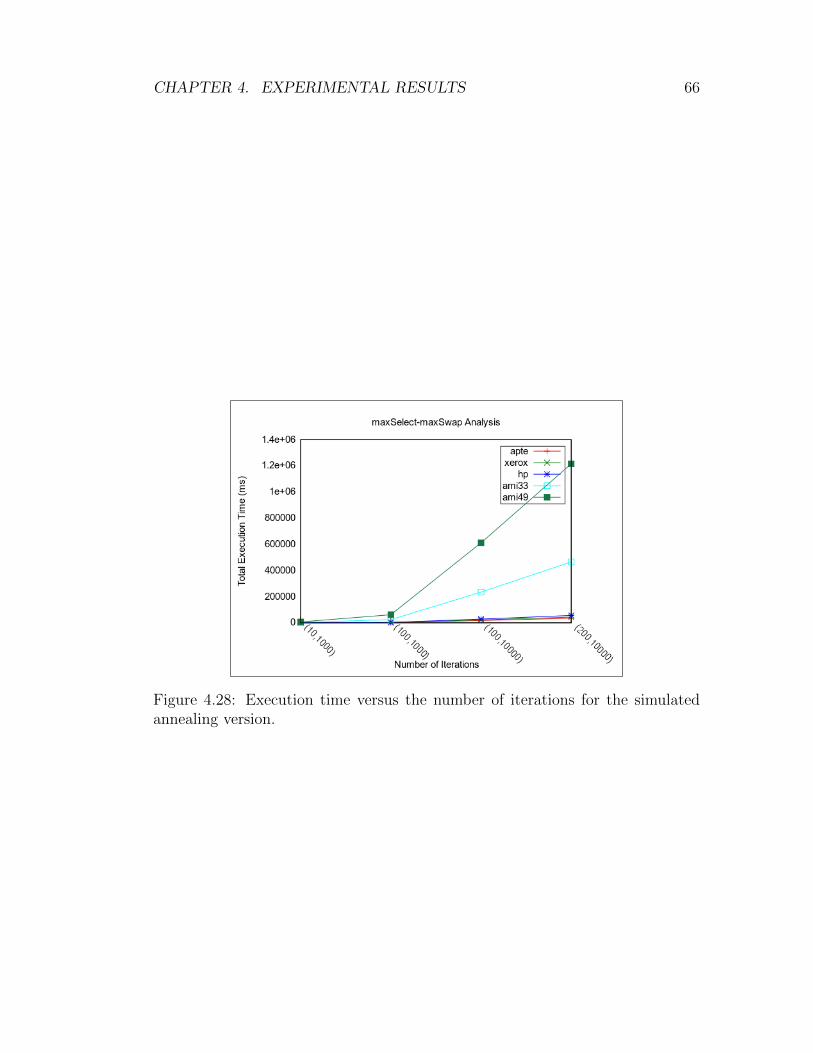
CHAPTER 4. EXPERIMENTAL RESULTS 66
Figure 4.28: Execution time versus the number of iterations for the simulatedannealing version.
Chapter 5
Conclusion and Future Work
We propose a novel algorithm to generate an application-specific NoC topology
minimizing total execution time and communication latency of a given set of
tasks in a reasonable time. The algorithms have two objectives: (i) selection of
appropriate processing cores that will be used in MPSoC, and (ii) placement of
selected processing cores on a given chip area in a way that total execution of the
given tasks and communication latency on chip are minimized. We achieve this
using two different techniques, namely a Genetic Algorithm based approach and
a 2D Bin Packing Algorithm. Our algorithms can cooperate with task scheduling
and core mapping algorithms during the generation of desired NoC and floor-
plan for MPSoC. The experimental results show that our algorithm improves
total communication latency up to 27% with moderate power consumption.
Our main concern is minimizing the overall execution latency among com-
municating processing cores while keeping the power consumption at acceptable
levels. However, power consumption in heterogeneous NoCs requires more atten-
tion. Therefore, we are planning to extend our framework to include power as
one of the major decision parameters along with execution latency and area. One
way of achieving power optimization is by clustering processors according to their
voltage levels, i.e., creating voltage islands within the chip area. We believe this
can be embedded into our framework thereby providing a more effective solution
for heterogeneous NoC design.
67

Bibliography
[1] S. Adya and I. Markov. Fixed-outline Floorplanning Through Better Local
Search. In Proceedings of the International Conference on Computer Design
(ICCD), pages 328–334, Piscataway, NJ, USA, 2001. IEEE.
[2] N. Banerjee, P. Vellanki, and K. S. Chatha. A Power and Performance Model
for Network-on-Chip Architectures. In Proceedings of the Conference on
Design, Automation and Test in Europe - Volume 2, DATE ’04, Washington,
DC, USA, 2004. IEEE Computer Society.
[3] V. Betz and J. Rose. VPR: A New packing, Placement and Routing Tool
for FPGA Research. In Proceedings of the 7th International Workshop on
Field-Programmable Logic and Applications, pages 213–222, London, UK,
1997. Springer-Verlag.
[4] H. Chan and I. Markov. Practical Slicing and Non-slicing Block-Packing
Without Simulated Annealing. In Proceedings of ACM/IEEE Great Lakes
Symposium on VLSI, pages 282–287, New York, NY, USA, 2004. ACM.
[5] H. H. Chan and I. L. Markov. Symmetries in Rectangular Block-packing.
In Proceedings of the International Workshop on Symmetry in Constraint
Satisfaction Problems, 2003.
[6] Y.-C. Chang, Y.-W. Chang, G.-M. Wu, and S.-W. Wu. B*-trees: A New
Representation for Non-slicing Floorplans. In Proceedings of the 37th Design
Automation Conference, pages 458–463, New York, NY, USA, 2000. ACM.
68
BIBLIOGRAPHY 69
[7] R. L. S. Ching, E. F. Y. Young, K. C. K. Leung, and C. Chu. Placement
Based Voltage Island Generation. In Proceedings of the 2006 IEEE/ACM
international conference on Computer-aided design, ICCAD ’06, pages 641–
646, New York, NY, USA, 2006. ACM.
[8] J. Cong, G. Nataneli, M. Romesis, and J. R. Shinnerl. An Area-optimality
Study of Floorplanning. In Proceedings of the International Symposium on
Physical Design, ISPD ’04, pages 78–83, New York, NY, USA, 2004. ACM.
[9] J. Cong, G. Nataneli, M. Romesis, and J. R. Shinnerl. An Area-optimality
Study of Floorplanning. In Proceedings of the International Symposium on
Physical Design, ISPD ’04, pages 78–83, New York, NY, USA, 2004. ACM.
[10] Y. Cui. Recursive Algorithm for Generating Two-staged Cutting Patterns
of Punched Strips. Mathematical & Computational Applications, 12(2):107–
115, 2007.
[11] R. Dick, D. Rhodes, and W. Wolf. TGFF: Task Graphs For Free. In Pro-
ceedings of the Sixth International Workshop on Hardware/Software Code-
sign (CODES/CASHE ’98), pages 97–101, Piscataway, NJ, USA, mar 1998.
IEEE.
[12] Embedded Microprocessor Benchmark Consortium (EEMBC). Embedded
System Synthesis Benchmarks Suite (E3S), 2011.
[13] M. R. Garey and D. S. Johnson. Computers and Intractability; A Guide to
the Theory of NP-Completeness. W. H. Freeman & Co., New York, NY,
USA, 1990.
[14] D. E. Goldberg. Genetic Algorithms in Search, Optimization and Machine
Learning. Addison-Wesley Longman Publishing Co., Inc., Boston, MA, USA,
1st edition, 1989.
[15] E. Hadjiconstantinou and M. Iori. A Hybrid Genetic Algorithm for the Two-
dimensional Single Large Object Placement Problem. European Journal of
Operational Research, 183(3):1150–1166, December 2007.
BIBLIOGRAPHY 70
[16] P. Healy and M. Creavin. An Optimal Algorithm for Rectangle Placement.
Operations Research Letters, 24(1-2):73–80, 1999.
[17] C. R. Houck, J. A. Joines, and M. G. Kay. A Genetic Algorithm for Function
Optimization: A Matlab Implementation. Technical Report NCSU-IE TR
95-09, Department of Computer Science, North Carolina State University,
1995.
[18] J. Hu, Y. Shin, N. Dhanwada, and R. Marculescu. Architecting Voltage
Islands in Core-based System-on-a-chip Designs. In Proceedings of the 2004
international symposium on Low power electronics and design, ISLPED ’04,
pages 180–185, New York, NY, USA, 2004. ACM.
[19] Y. Hu, Y. Zhu, H. Chen, R. Graham, and C.-K. Cheng. Communica-
tion Latency Aware Low Power NoC Synthesis. In Proceedings of the 43rd
ACM/IEEE Design Automation Conference, pages 574–579, New York, NY,
USA, 0-0 2006. ACM.
[20] W. Jang and D. Pan. A3MAP: Architecture-Aware Analytic Mapping for
Networks-on-Chip. In Proceedings of the 15th Asia and South Pacific Design
Automation Conference (ASP-DAC), pages 523–528, Piscataway, NJ, USA,
jan. 2010. IEEE.
[21] Y.-P. Joo, S. Kim, and S. Ha. On-chip Communication Architecture Explo-
ration for Processor-pool-based MPSoC. In Proceedings of the Conference
on Design, Automation and Test in Europe, DATE ’09, pages 466–471, 3001
Leuven, Belgium, Belgium, 2009. European Design and Automation Associ-
ation.
[22] M. R. Kakoee, F. Angiolini, A. Pullini, C. Seiculescu, and L. Benini. A
Floorplan-aware Interactive Tool Flow for NoC Design and Synthesis. In
Proceedings of the SoC Conference (SOCC), pages 65 – 68, New York, USA,
9-11 September 2009. IEEE Press.
[23] J.-G. Kim and Y.-D. Kim. A Linear Programming-based Algorithm for
Floorplanning in VLSI Design. IEEE Transactions on Computer-Aided De-
sign of Integrated Circuits and Systems, 22(5):584–592, may 2003.
BIBLIOGRAPHY 71
[24] S. Kumar, A. Jantsch, M. Millberg, J. Oberg, J.-P. Soininen, M. Forsell,
K. Tiensyrja, and A. Hemani. A Network on Chip Architecture and Design
Methodology. In Proceedings of the IEEE Computer Society Annual Sym-
posium on VLSI, ISVLSI’02, pages 117–124, Piscataway, NJ, USA, 2002.
IEEE.
[25] U. Lauther. A Min-cut Placement Algorithm for General Cell Assemblies
Based on a Graph Representation. In Proceedings of the 16th Design Au-
tomation Conference, DAC ’79, pages 1–10, Piscataway, NJ, USA, 1979.
IEEE Press.
[26] G. Leary and K. S. Chatha. Automated Technique for Design of NoC with
Minimal Communication Latency. In Proceedings of the 7th IEEE/ACM
International Conference on Hardware/Software Codesign and System Syn-
thesis, CODES+ISSS ’09, pages 471–480, New York, NY, USA, 2009. ACM.
[27] W.-P. Lee, H.-Y. Liu, and Y.-W. Chang. Voltage Island Aware Floorplanning
for Power and Timing Optimization. In Proceedings of the 2006 IEEE/ACM
international conference on Computer-aided design, ICCAD ’06, pages 389–
394, New York, NY, USA, 2006. ACM.
[28] J.-M. Lin and Y.-W. Chang. TCG-S:Orthogonal Coupling of P*-admissible
Representations for General Floorplans. In Proceedings of the 39th Design
Automation Conference, pages 842–847, Piscataway, NJ, USA, 2002. IEEE.
[29] A. Lodi, S. Martello, and D. Vigo. Heuristic and Metaheuristic Approaches
for a Class of Two-Dimensional Bin Packing Problems. INFORMS Journal
on Computing, 11(4):345–357, 1999.
[30] Q. Ma and E. F. Y. Young. Voltage island-driven Floorplanning. In Pro-
ceedings of the 2007 IEEE/ACM international conference on Computer-aided
Design, ICCAD ’07, pages 644–649, Piscataway, NJ, USA, 2007. IEEE Press.
[31] G. Martin. Overview of the MPSoC Design Challenge. In Proceedings of the
43rd Annual Design Automation Conference, DAC ’06, pages 274–279, New
York, NY, USA, 2006. ACM.

BIBLIOGRAPHY 72
[32] S. Meftali, F. Gharsalli, F. Rousseau, and A. A. Jerraya. Automatic
Code-transformation and Architecture Refinement for Application-specific
Multiprocessor SoCs with Shared Memory. In Proceedings of the IFIP
TC10/WG10.5 Eleventh International Conference on Very Large Scale In-
tegration of Systems-on/Chip: SOC Design Methodologies, VLSI-SOC ’01,
2001.
[33] S. Murali and G. De Micheli. SUNMAP: A Tool for Automatic Topology
Selection and Generation for NoCs. In Design Automation Conference, 2004.
Proceedings. 41st, pages 914–919, july 2004.
[34] S. Murali, P. Meloni, F. Angiolini, D. Atienza, S. Carta, L. Benini, G. De
Micheli, and L. Raffo. Designing Application-Specific Networks on Chips
with Floorplan Information. In Proceedings of the IEEE/ACM International
Conference on Computer-Aided Design (ICCAD ’06), pages 355–362, Pis-
cataway, NJ, USA, nov. 2006. IEEE.
[35] S. Murali and G. D. Micheli. Bandwidth-Constrained Mapping of Cores
onto NoC Architectures. In Proceedings of the Design, Automation and Test
in Europe Conference and Exhibition, volume 2, pages 896–901, Piscataway,
NJ, USA, 2004. IEEE.
[36] U. Y. Ogras, J. Hu, and R. Marculescu. Key Research Problems in NoC
Design: A Holistic Perspective. In Proceedings of the 3rd IEEE/ACM/IFIP
International Conference on Hardware/Software Codesign and System Syn-
thesis, CODES+ISSS ’05, pages 69–74, New York, NY, USA, 2005. ACM.
[37] C. Ostler and K. S. Chatha. An ILP Formulation for System-level Appli-
cation Mapping on Network Processor Architectures. In Proceedings of the
Conference on Design, Automation and Test in Europe, DATE ’07, pages
99–104, San Jose, CA, USA, 2007. EDA Consortium.
[38] L. Pal. A Genetic Algorithm for the Two-dimensional Single Large Ob-
ject Placement Problem. In Proceedings of 3rd Romanian-Hungarian Joint
Symposium on Applied Computational Intelligence, 2006.

BIBLIOGRAPHY 73
[39] M. Pan, N. Viswanathan, and C. Chu. An Efficient and Effective Detailed
Placement Algorithm. In Proceedings of the IEEE/ACM International Con-
ference on Computer-Aided Design, ICCAD ’05, pages 48–55, Washington,
DC, USA, 2005. IEEE Computer Society.
[40] M. Romesis. FEKO-A Suite (Floorplanning Examples with Known Optimal
Area), 2004.
[41] V. Schnecke and O. Vornberger. Hybrid Genetic Algorithms for Constrained
Placement Problems. IEEE Transactions on Evolutionary Computation,
1(4):266–277, 1997.
[42] K. Srinivasan and K. S. Chatha. A Methodology for Layout Aware Design
and Optimization of Custom Network-on-Chip Architectures. In Proceedings
of the 7th International Symposium on Quality Electronic Design, ISQED
’06, pages 352–357, Washington, DC, USA, 2006. IEEE Computer Society.
[43] K. Srinivasan and K. S. Chatha. Integer Linear Programming and Heuristic
Techniques for System-level Low Power Scheduling on Multiprocessor Ar-
chitectures under Throughput Constraints. Integration, the VLSI Journal,
40:326–354, April 2007.
[44] K. Srinivasan, K. S. Chatha, and G. Konjevod. Application Specific Network-
on-chip Design with Guaranteed Quality Approximation Algorithms. In
Proceedings of the Asia and South Pacific Design Automation Conference,
ASP-DAC ’07, pages 184–190, Washington, DC, USA, 2007. IEEE Computer
Society.
[45] A. Stoica, R. Zebulum, D. Keymeulen, and J. Lohn. On Polymorphic Circuits
and Their Design Using Evolutionary Algorithms. In Proceedings of IASTED
International Conference on Applied Informatics (AI’02), Insbruck, Austria,
2002.
[46] H. Terashima-Marın, E. J. Flores-Alvarez, and P. Ross. Hyper-heuristics
and Classifier Systems for Solving 2D-regular Cutting Stock Problems. In
Proceedings of the Conference on Genetic and Evolutionary Computation,
GECCO ’05, pages 637–643, New York, NY, USA, 2005. ACM.
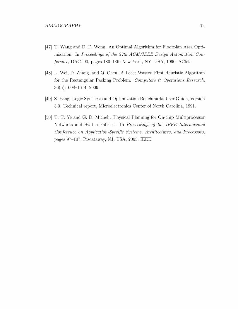
BIBLIOGRAPHY 74
[47] T. Wang and D. F. Wong. An Optimal Algorithm for Floorplan Area Opti-
mization. In Proceedings of the 27th ACM/IEEE Design Automation Con-
ference, DAC ’90, pages 180–186, New York, NY, USA, 1990. ACM.
[48] L. Wei, D. Zhang, and Q. Chen. A Least Wasted First Heuristic Algorithm
for the Rectangular Packing Problem. Computers & Operations Research,
36(5):1608–1614, 2009.
[49] S. Yang. Logic Synthesis and Optimization Benchmarks User Guide, Version
3.0. Technical report, Microelectronics Center of North Carolina, 1991.
[50] T. T. Ye and G. D. Micheli. Physical Planning for On-chip Multiprocessor
Networks and Switch Fabrics. In Proceedings of the IEEE International
Conference on Application-Specific Systems, Architectures, and Processors,
pages 97–107, Piscataway, NJ, USA, 2003. IEEE.
Appendix A
Sample Layouts
A.1 TGFF-Semi Synthetic Layouts
The layouts generated that contain 256, 512, 1024 and 2048 processing cores for
a task graph with 2048 tasks are shown below.
75
APPENDIX A. SAMPLE LAYOUTS 76
Figure A.1: Sample layout containing 256 processing cores for a task graph with
2048 tasks.

APPENDIX A. SAMPLE LAYOUTS 77
Figure A.2: Sample layout containing 512 processing cores for a task graph with
2048 tasks.

APPENDIX A. SAMPLE LAYOUTS 78
Figure A.3: Sample layout containing 1024 processing cores for a task graph with
2048 tasks.
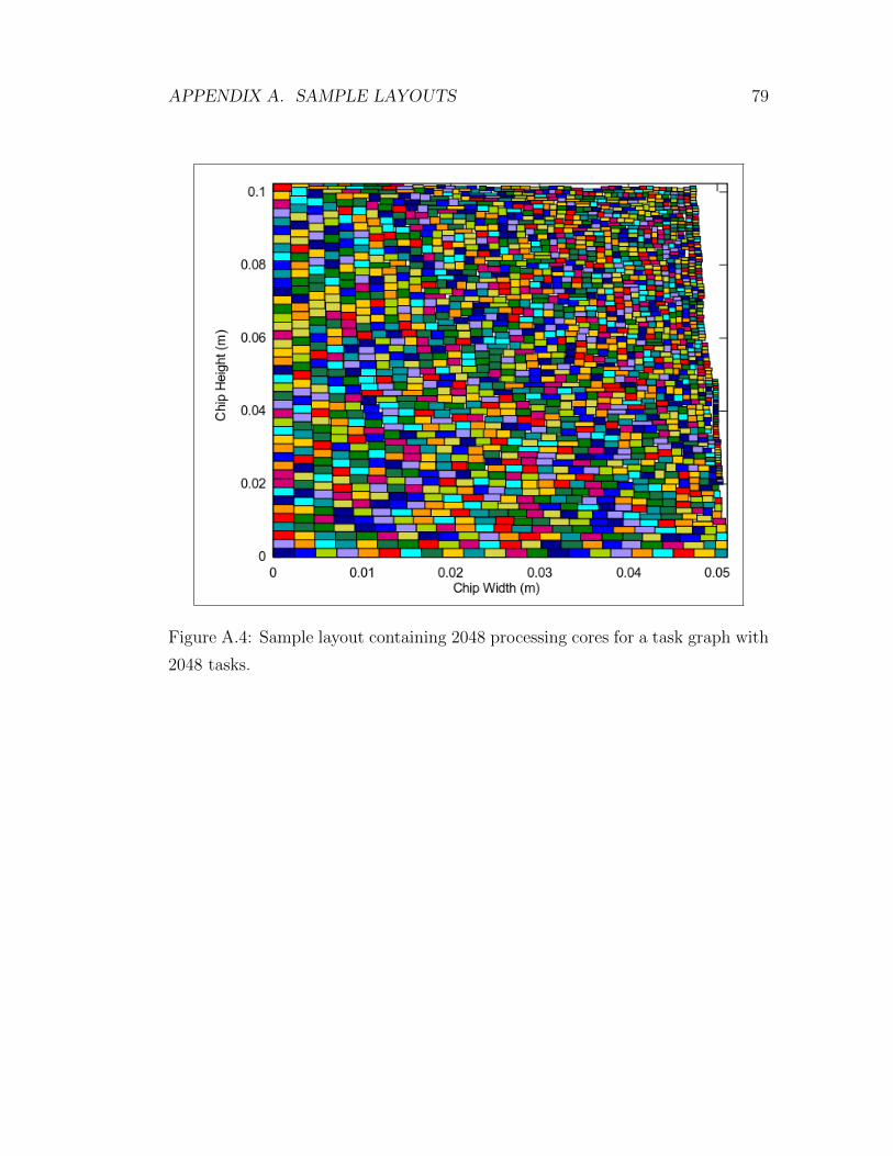
APPENDIX A. SAMPLE LAYOUTS 79
Figure A.4: Sample layout containing 2048 processing cores for a task graph with
2048 tasks.

APPENDIX A. SAMPLE LAYOUTS 80
A.2 Minimum Dead Area Layouts
Figure A.5: Sample layout containing 300 processing cores with dead area 2.3%.
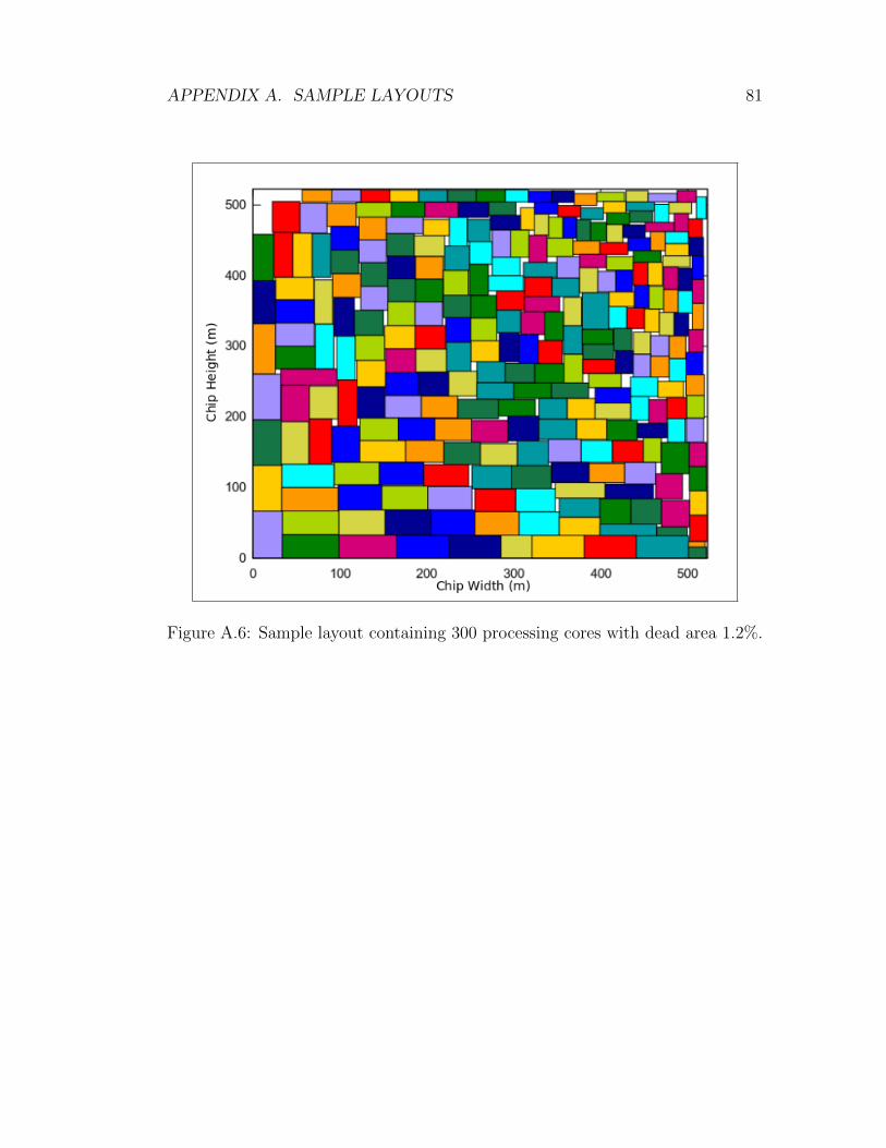
APPENDIX A. SAMPLE LAYOUTS 81
Figure A.6: Sample layout containing 300 processing cores with dead area 1.2%.
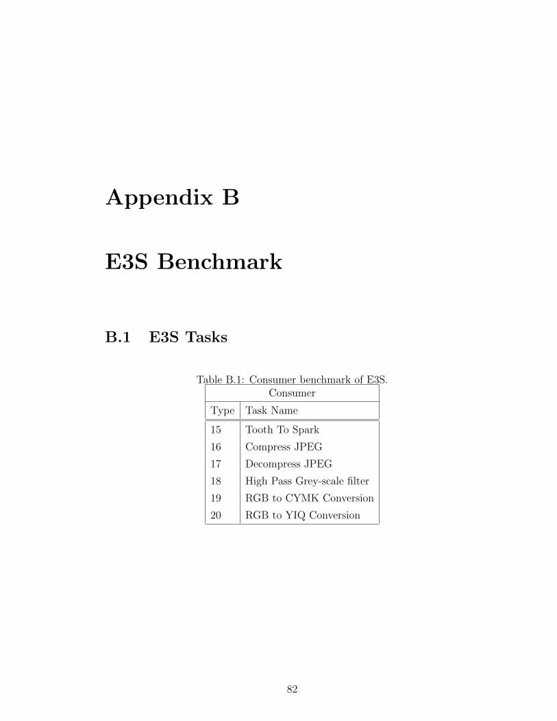
Appendix B
E3S Benchmark
B.1 E3S Tasks
Table B.1: Consumer benchmark of E3S.Consumer
Type Task Name
15 Tooth To Spark
16 Compress JPEG
17 Decompress JPEG
18 High Pass Grey-scale filter
19 RGB to CYMK Conversion
20 RGB to YIQ Conversion
82
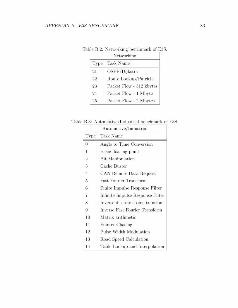
APPENDIX B. E3S BENCHMARK 83
Table B.2: Networking benchmark of E3S.
Networking
Type Task Name
21 OSPF/Dijkstra
22 Route Lookup/Patricia
23 Packet Flow - 512 kbytes
24 Packet Flow - 1 Mbyte
25 Packet Flow - 2 Mbytes
Table B.3: Automotive/Industrial benchmark of E3S.
Automotive/Industrial
Type Task Name
0 Angle to Time Conversion
1 Basic floating point
2 Bit Manipulation
3 Cache Buster
4 CAN Remote Data Request
5 Fast Fourier Transform
6 Finite Impulse Response Filter
7 Infinite Impulse Response Filter
8 Inverse discrete cosine transfom
9 Inverse Fast Fourier Transform
10 Matrix arithmetic
11 Pointer Chasing
12 Pulse Width Modulation
13 Road Speed Calculation
14 Table Lookup and Interpolation
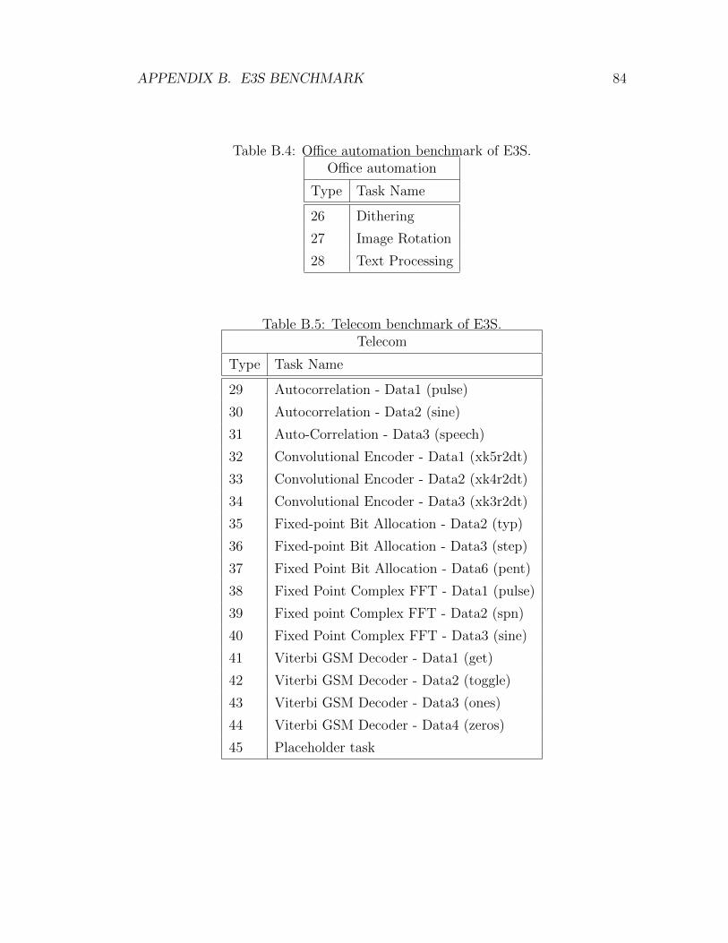
APPENDIX B. E3S BENCHMARK 84
Table B.4: Office automation benchmark of E3S.Office automation
Type Task Name
26 Dithering
27 Image Rotation
28 Text Processing
Table B.5: Telecom benchmark of E3S.Telecom
Type Task Name
29 Autocorrelation - Data1 (pulse)
30 Autocorrelation - Data2 (sine)
31 Auto-Correlation - Data3 (speech)
32 Convolutional Encoder - Data1 (xk5r2dt)
33 Convolutional Encoder - Data2 (xk4r2dt)
34 Convolutional Encoder - Data3 (xk3r2dt)
35 Fixed-point Bit Allocation - Data2 (typ)
36 Fixed-point Bit Allocation - Data3 (step)
37 Fixed Point Bit Allocation - Data6 (pent)
38 Fixed Point Complex FFT - Data1 (pulse)
39 Fixed point Complex FFT - Data2 (spn)
40 Fixed Point Complex FFT - Data3 (sine)
41 Viterbi GSM Decoder - Data1 (get)
42 Viterbi GSM Decoder - Data2 (toggle)
43 Viterbi GSM Decoder - Data3 (ones)
44 Viterbi GSM Decoder - Data4 (zeros)
45 Placeholder task

APPENDIX B. E3S BENCHMARK 85
B.2 E3S Processors
Table B.6: E3S processor list.
ID Height Width Name
0 0.0031 0.0031 AMD ElanSC520-133 MHz – square
1 0.00648 0.00648 AMD K6-2 450 – square
2 0.00648 0.00648 AMD K6-2E 400Mhz/ACR – square
3 0.00648 0.00648 AMD K6-2E+ 500Mhz/ACR – square
4 0.00837 0.00837 AMD K6-IIIE+ 550Mhz/ACR – square
5 0.0010 0.0010 Analog Devices 21065L - 60 MHz – square
6 0.00268 0.00268 IBM PowerPC 405GP - 266 Mhz – square
7 0.0098 0.0098 IBM PowerPC 750CX - 500 MHz – square
8 0.00173 0.00173 IDT32334-100 MHz – square
9 0.00173 0.00173 IDT79RC32364-100 – square
10 0.00173 0.00173 IDT79RC32V334-150 – square
11 0.0062 0.0062 IDT79RC64575-250MHz – square
12 0.0010 0.0010 Imsys Cjip 40 Mhz – square
13 0.0010 0.0010 Motorola MPC555 - 40MHz – square
14 0.00438 0.00438 NEC VR5432 - 167 MHz – square 1.0
15 0.00122 0.00122 ST20C2 50 Mhz – square 1.0 0.0
16 0.0010 0.0010 TI TMS320C6203-300MHz – square 1.0
17 0.0062 0.00155 AMD ElanSC520-133 MHz – rectangle
18 0.013 0.00324 AMD K6-2 450 – rectangle 1.0
19 0.013 0.00324 AMD K6-2E 400Mhz/ACR – rectangle
20 0.013 0.00324 AMD K6-2E+ 500Mhz/ACR – rectangle
21 0.0167 0.00418 AMD K6-IIIE+ 550Mhz/ACR – rectangle
22 0.0020 5.0E-4 Analog Devices 21065L - 60 MHz – rectangle
23 0.00537 0.00134 IBM PowerPC 405GP - 266 Mhz – rectangle
24 0.0196 0.0049 IBM PowerPC 750CX - 500 MHz – rectangle
25 0.00346 8.66E-4 IDT32334-100 MHz – rectangle
26 0.00346 8.66E-4 IDT79RC32364-100 – rectangle
27 0.00346 8.66E-4 IDT79RC32V334-150 – rectangle
28 0.0124 0.0031 IDT79RC64575-250MHz – rectangle
29 0.0020 5.0E-4 Imsys Cjip 40 Mhz – rectangle
30 0.0020 5.0E-4 Motorola MPC555 - 40MHz – rectangle
31 0.00876 0.00219 NEC VR5432 - 167 MHz – rectangle
32 0.00245 6.12E-4 ST20C2 50 Mhz – rectangle 1.0
33 0.0020 5.0E-4 TI TMS320C6203-300MHz – rectangle
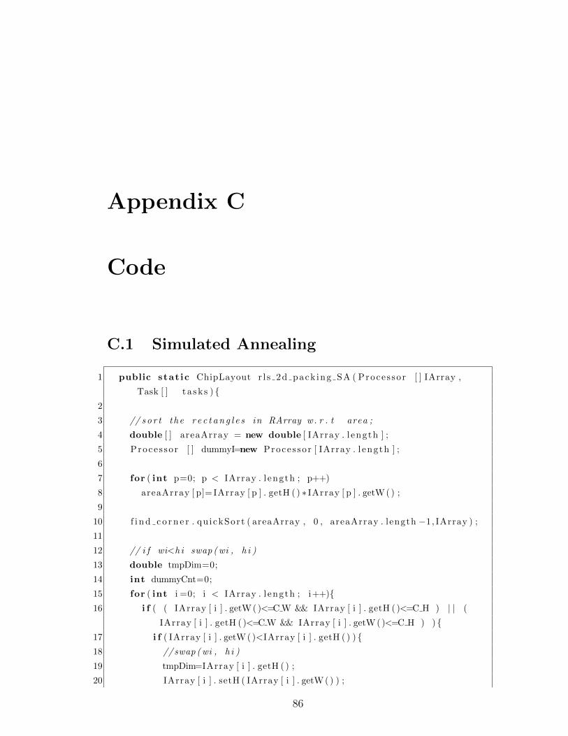
Appendix C
Code
C.1 Simulated Annealing
1 public stat ic ChipLayout r l s 2d pack ing SA ( Proces sor [ ] IArray ,
Task [ ] t a sk s ) {2
3 // s o r t the r e c t a n g l e s in RArray w. r . t area ;
4 double [ ] areaArray = new double [ IArray . l ength ] ;
5 Proces sor [ ] dummyI=new Proces sor [ IArray . l ength ] ;
6
7 for ( int p=0; p < IArray . l ength ; p++)
8 areaArray [ p]= IArray [ p ] . getH ( ) ∗ IArray [ p ] . getW() ;
9
10 f i n d c o r n e r . qu ickSort ( areaArray , 0 , areaArray . length −1, IArray ) ;
11
12 // i f wi<h i swap ( wi , h i )
13 double tmpDim=0;
14 int dummyCnt=0;
15 for ( int i =0; i < IArray . l ength ; i++){16 i f ( ( IArray [ i ] . getW()<=CW && IArray [ i ] . getH ( )<=C H ) | | (
IArray [ i ] . getH ( )<=CW && IArray [ i ] . getW()<=C H ) ) {17 i f ( IArray [ i ] . getW()<IArray [ i ] . getH ( ) ) {18 //swap ( wi , h i )
19 tmpDim=IArray [ i ] . getH ( ) ;
20 IArray [ i ] . setH ( IArray [ i ] . getW() ) ;
86

APPENDIX C. CODE 87
21 IArray [ i ] . setW(tmpDim) ;
22 }23 dummyI [ i ]=new Proces sor ( ) ;
24 dummyI [ dummyCnt]= IArray [ i ] ;
25 dummyCnt++;
26 }27 }28
29 IArray=null ;
30 IArray= new Proces sor [ dummyCnt ] ;
31 for ( int k=0; k<dummyCnt ; k++){32 IArray [ k]=new Proces sor ( ) ;
33 IArray [ k]=dummyI [ k ] ;
34 }35
36 TEMPERATURE = ( con f i gurat i onParamete r s . wireDelayPerBit+1)∗(CW +
C H) ;
37 COOLING SCHEDULE = TEMPERATURE;
38 Proces sor [ ] newI = null ; // s t o r e s packed p r o c e s s o r s
39 ChipLayout currentLayout = new ChipLayout (CW, C H) ;
40 ChipLayout loca lBestLayout = new ChipLayout (CW, C H) ;
41 ChipLayout previousLayout = new ChipLayout (CW, C H) ;
42 newI = packingPEs ( IArray ) ;
43 currentLayout . p r o c e s s o r s = new Proces sor [ newI . l ength ] ;
44 currentLayout . p r o c e s s o r s = newI ;
45 previousLayout = la t ency . ca lcLatency ( currentLayout , t a sk s ) ;
46
47 // s e t l o c a l B e s t L a y o u t to the f i r s t l a y o u t
48 loca lBestLayout . ove ra l lLa t ency = previousLayout . ove ra l lLa t ency ;
49 loca lBestLayout . overa l lPower = previousLayout . overa l lPower ;
50 loca lBestLayout . p r o c e s s o r s = previousLayout . p r o c e s s o r s ;
51 Proces sor swap ;
52 Random r = new Random( ) ;
53 for ( int i =0; i < CALLMAX && (TEMPERATURE > 0) ; i++){54
55 i f ( IArray . l ength > 1) {// i f t h e r e i s on ly one p r o c e s s o r l e f t ,
then s t op . no combination remains .
56 a = r . next Int ( IArray . l ength ) ;
57 b = r . next Int ( IArray . l ength ) ;
58 }
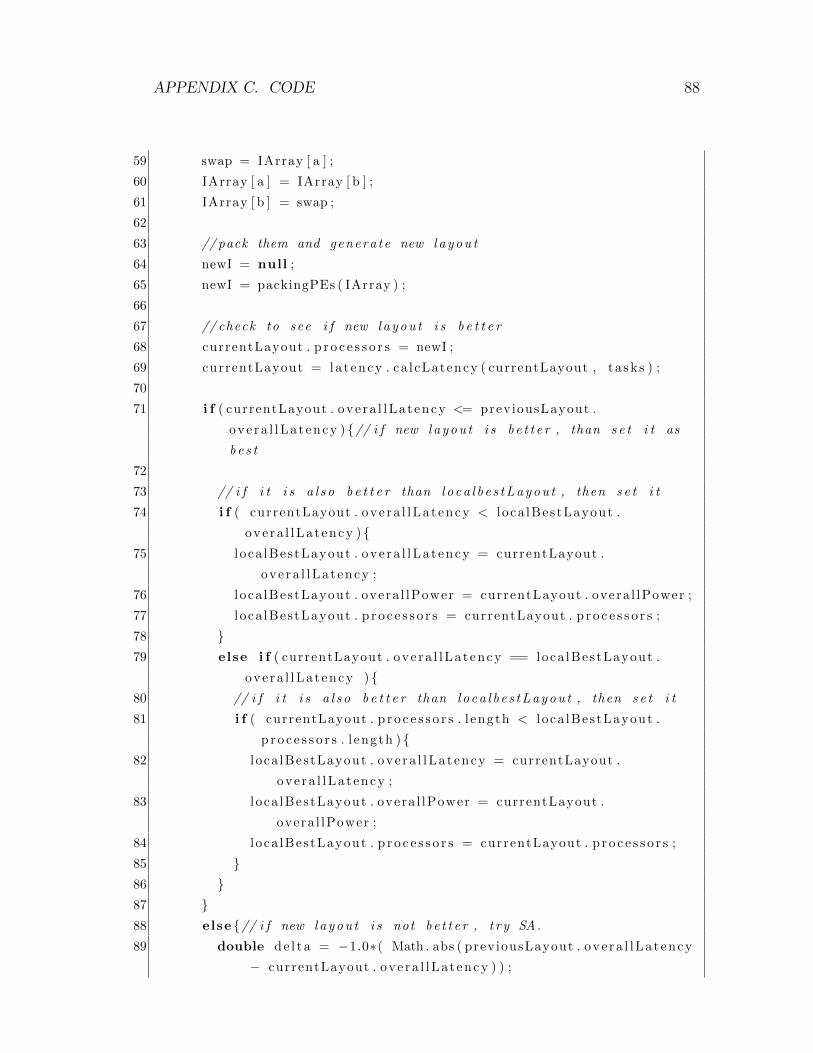
APPENDIX C. CODE 88
59 swap = IArray [ a ] ;
60 IArray [ a ] = IArray [ b ] ;
61 IArray [ b ] = swap ;
62
63 // pack them and genera te new l a y o u t
64 newI = null ;
65 newI = packingPEs ( IArray ) ;
66
67 // check to see i f new l a y o u t i s b e t t e r
68 currentLayout . p r o c e s s o r s = newI ;
69 currentLayout = la t ency . ca lcLatency ( currentLayout , t a sk s ) ;
70
71 i f ( currentLayout . ove ra l lLa t ency <= previousLayout .
ove ra l lLa t ency ) {// i f new l a y o u t i s b e t t e r , than s e t i t as
b e s t
72
73 // i f i t i s a l s o b e t t e r than l o c a l b e s t L a y o u t , then s e t i t
74 i f ( currentLayout . ove ra l lLa t ency < l oca lBestLayout .
ove ra l lLa t ency ) {75 loca lBestLayout . ove ra l lLa t ency = currentLayout .
ove ra l lLa t ency ;
76 loca lBestLayout . overa l lPower = currentLayout . overa l lPower ;
77 loca lBestLayout . p r o c e s s o r s = currentLayout . p r o c e s s o r s ;
78 }79 else i f ( currentLayout . ove ra l lLa t ency == loca lBestLayout .
ove ra l lLa t ency ) {80 // i f i t i s a l s o b e t t e r than l o c a l b e s t L a y o u t , then s e t i t
81 i f ( currentLayout . p r o c e s s o r s . l ength < l oca lBestLayout .
p r o c e s s o r s . l ength ) {82 loca lBestLayout . ove ra l lLa t ency = currentLayout .
ove ra l lLa t ency ;
83 loca lBestLayout . overa l lPower = currentLayout .
overa l lPower ;
84 loca lBestLayout . p r o c e s s o r s = currentLayout . p r o c e s s o r s ;
85 }86 }87 }88 else {// i f new l a y o u t i s not b e t t e r , t r y SA.
89 double de l t a = −1.0∗( Math . abs ( previousLayout . ove ra l lLa t ency
− currentLayout . ove ra l lLa t ency ) ) ;
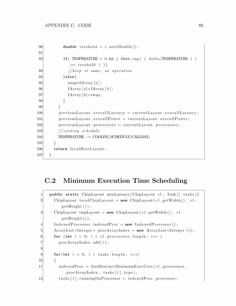
APPENDIX C. CODE 89
90 double t r e sho l d = r . nextDouble ( ) ;
91
92 i f ( TEMPERATURE > 0 && ( Math . exp ( ( de l t a /TEMPERATURE ) )
>= tr e sho l d ) ) {93 // keep i t same ; no op era t ion
94 } else {95 swap=IArray [ a ] ;
96 IArray [ a]= IArray [ b ] ;
97 IArray [ b]=swap ;
98 }99 }100 previousLayout . ove ra l lLa t ency = currentLayout . ove ra l lLa t ency ;
101 previousLayout . overa l lPower = currentLayout . overa l lPower ;
102 previousLayout . p r o c e s s o r s = currentLayout . p r o c e s s o r s ;
103 // c o o l i n g s c h e d u l e
104 TEMPERATURE −= COOLING SCHEDULE/CALLMAX;
105 }106 return l oca lBestLayout ;
107 }
C.2 Minimum Execution Time Scheduling
1 public stat ic ChipLayout minLatency ( ChipLayout c l , Task [ ] t a sk s ) {2 ChipLayout localChipLayout = new ChipLayout ( c l . getWidth ( ) , c l .
getHeight ( ) ) ;
3 ChipLayout tmpLayout = new ChipLayout ( c l . getWidth ( ) , c l .
getHeight ( ) ) ;
4 IndexedProcessor indexedProc = new IndexedProcessor ( ) ;
5 ArrayList<Integer> procArrayIndex = new ArrayList<Integer >() ;
6 for ( int i = 0 ; i < c l . p r o c e s s o r s . l ength ; i++ )
7 procArrayIndex . add ( i ) ;
8
9 for ( int i = 0 ; i < ta sk s . l ength ; i++)
10 {11 indexedProc = findDistinctMinimumExecCore ( c l . p roce s so r s ,
procArrayIndex , ta sk s [ i ] . type ) ;
12 ta sk s [ i ] . runningOnProcessor = indexedProc . p ro c e s s o r ;
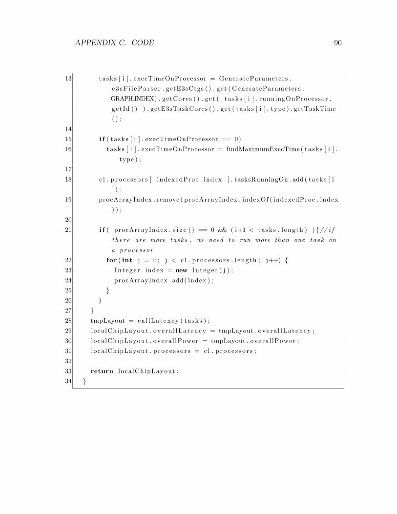
APPENDIX C. CODE 90
13 ta sk s [ i ] . execTimeOnProcessor = GenerateParameters .
e 3 sF i l ePa r s e r . getE3sCtgs ( ) . get ( GenerateParameters .
GRAPH INDEX) . getCores ( ) . get ( ta sk s [ i ] . runningOnProcessor .
ge t Id ( ) ) . getE3sTaskCores ( ) . get ( ta sk s [ i ] . type ) . getTaskTime
( ) ;
14
15 i f ( ta sk s [ i ] . execTimeOnProcessor == 0)
16 ta sk s [ i ] . execTimeOnProcessor = findMaximumExecTime ( ta sk s [ i ] .
type ) ;
17
18 c l . p r o c e s s o r s [ indexedProc . index ] . tasksRunningOn . add ( ta sk s [ i
] ) ;
19 procArrayIndex . remove ( procArrayIndex . indexOf ( indexedProc . index
) ) ;
20
21 i f ( procArrayIndex . s i z e ( ) == 0 && ( i+1 < ta sk s . l ength ) ) {// i f
t h e r e are more tasks , we need to run more than one t a s k on
a p r o c e s s o r
22 for ( int j = 0 ; j < c l . p r o c e s s o r s . l ength ; j++) {23 In t eg e r index = new I n t eg e r ( j ) ;
24 procArrayIndex . add ( index ) ;
25 }26 }27 }28 tmpLayout = ca l lLa t ency ( ta sk s ) ;
29 localChipLayout . ove ra l lLa t ency = tmpLayout . ove ra l lLa tency ;
30 localChipLayout . overa l lPower = tmpLayout . overa l lPower ;
31 localChipLayout . p r o c e s s o r s = c l . p r o c e s s o r s ;
32
33 return loca lChipLayout ;
34 }