application of continuous extended scanning techniques to the simultaneous detection of raman...
TRANSCRIPT
JOURNAL OF RAMAN SPECTROSCOPY, VOL. 26, 777-785 (1995)
Application of Continuous Extended Scanning Techniques to the Simultaneous Detection of Raman Scattering and Photoluminescence from Calcium Disilicates using Visible and Near- Infrared Excitation*
Chris Dyer? and Brian J. E. Smith Raman Group, Transducer Systems Division, Renishaw plc, Old Town, Wotton-Under-Edge, Gloucestershire GL12 7DH, UK
A novel method of data acquisition is described for spectrographs employing charge-coupled device (CCD) detec- tion. The technique, called continuous extended (CE) scanning, allows data collection over the full spectral range of the spectrograph, rather than a limited window determined by the wavelength, spectral dispersion, spectrograph focal length and detector dimensions. The CE method removes the need to sacrifice resolution for spectral range or the need to record and splice many spectral segments to reproduce a full-range spectrum. The advantages of this method are discussed and the capability is demonstrated with respect to several calcium disilicate minerals, recently shown to exhibit intriguing behaviour under near-infrared (NIR) excitation, including intense photoluminescence. Data obtained using both visible (514.5 nm) and NIR (779.1 nm) excitation are presented and the results are briefly discussed in the light of recent Fourier transform Raman studies using 1064.1 nm excitation.
INTRODUCTION
A revival in the fortunes of Raman spectroscopic analysis has certainly occurred within the past 10 years. This is clearly evidenced by the growing number of aca- demic research papers and Raman-based publications, a number of new applications of the Raman effect in analytical studies, and the growth in the number of instrument companies offering dedicated Raman instrumentation. The resurgence has been led by improvements in analytical methods and instrumen- tation. The improvements have rendered many experi- ments easier to perform and more likely to yield a positive result or have shortened the time-scale for data collection. The use of the adapted Michelson interfer- ometer for Fourier transform (FT) Raman spectroscopy and the re-emergence of the dispersive spectrograph based on the charge-coupled device (CCD) detector are the most obvious examples of the advances made.
Spectrographs have traditionally suffered from a limited spectral range, often called the spectral 'window'. This paper describes a novel method for con- trolling and collecting data utilizing the CCD's capabil- ity for on-chip charge movement to overcome this limitation. Two synthetic calcium disilicate minerals are used to demonstrate the technique, and the simulta- neous determination of both Raman scattering (RS) and photoluminescence (PL) spectra over a 500 nm spectral range is reported.
* This paper is dedicated to Professor D. A. Long on the occasion
t Author to whom correspondence should be addressed. of his 70th birthday.
CCC 0377-0486/95/090777-09 0 1995 by John Wiley & Sons, Ltd.
In addition, near-infrared (NIR) excitation at 779.1 nm is used to provide an intermediate point between 514.5 and 1064.1 nm excitation. Recording Raman spectra with two widely separated excitation wave- lengths allows differentiation of RS and PL, in those areas where the RS and PL overlap.
EXPERIMENTAL
The calcium disilicates were supplied by Blue Circle via Mr Roger Gollop. The materials were synthesized from selected mineral feedstocks rather than pure chemical reagents. Crystal structures were determined using powder x-ray diffraction (PXRD), and both samples were analysed for elemental composition using induc- tively coupled plasma atomic emission spectroscopy (ICP-AES). PXRD confirmed the crystal structures as /?- and y-Ca,SiO,, often abbreviated as /?- and y-C2S. The /?-form is properly thermodynamically unstable at room temperature,'*2 although its conversion into the stable y-form appears minimal. ICP-AES revealed several transition metal ion impurities at the 10-100 ppm level.
Two Renishaw Imaging Raman microscope systems were employed to collect the RS and PL data. This device has been well reviewed el~ewhere,~." so only rele- vant experimental details will be given here.
A system employing 514.5 nm excitation (argon ion gas laser) and standard optics including a 1800 grooves m n - ' grating was used. The configuration allowed most efficient operation between 450 and 950 nm. Power of 2-3 mW was incident on the sample in a 2 pm diameter spot through a standard x50 microscope
Received 23 March 1995 Accepted (revised) I2 April 1995

778 C. DYER AND B. J. E. SMITH
objective. The spectral resolution was 3-4 cm-'. A separate system was NIR-optimized for 600-1000 nm. The optimized optics included a 1200 grooves mm-' grating and an AlGaAs laser diode (LD) emitting at 779.1 nm was used for excitation. The excitation power, spot size and collection optics magnification were the same as for the green system. The system was set to give 2-3 cm-' spectral resolution.
In both cases, resolution was determined by measur- ing the FWHM of the laser line by curve fitting. No data treatment was applied to the spectra, which are presented as intensity (arbitrary units) us. wavenumber shift (cm - ' in air).
RESULTS AND DISCUSSION
Early studies on calcium silicate^^.^ showed that strong RS could be obtained using visible excitation, especially from synthetic minerals, although strong fluorescence often interfered. In contrast to suggestions in the earlier work, long-wavelength excitation was shown to be a poor solution;' this was linked to transition metal impurity content. This has led to a small but expanding body of literature7-" concerned with the cause and nature of the intense PL.
Figures 1 and 2 show the FT-Raman spectra (1064.1 nm excitation) of the two minerals under investigation. Comparison with accepted literature v a l ~ e s ~ . ~ and the current work shows that the spectra are definitely not due to Raman scattering.
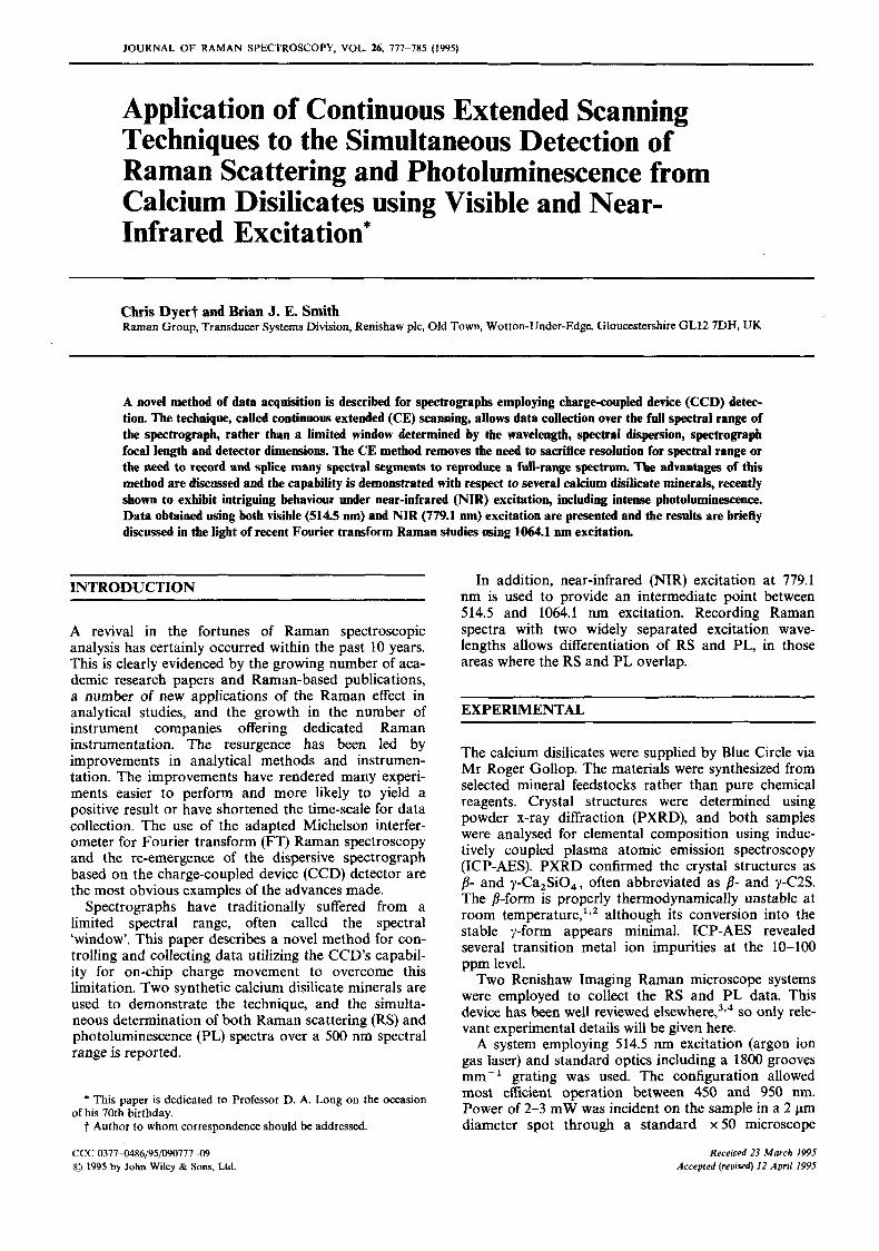
These may be compared with the clear silicate vibra- tional features obtained using 514.5 nm excitation, shown in Figs 3 and 4. The band positions, shapes and relative intensities correlate well with previous studies.
Despite a PL background being clearly visible, the RS features are easily resolved with good signal-to-noise ratio (SNR) after only 25 s.
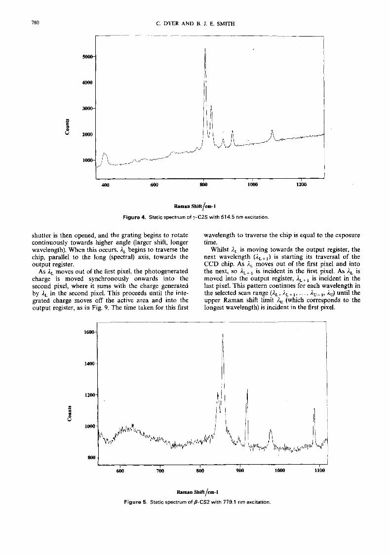
However, it should be noted that the spectrograph spectral 'window' covers less than 950 an-' at this wavelength. Although this is adequate in many cases, a wider spectral coverage is often desirable. With 779.1 nm excitation the spectral 'window' is reduced to less than 600 an-', as shown in Figs 5 and 6. This includes the compensation made by the lower dispersion, higher NIR efficiency 1200 grooves mm-' grating.
A method to overcome the spectrograph's restriction to a limited 'window' is obviously desirable. For example, the combination of RS and PL measurements is very attractive for many systems, and requires the ability to record spectral ranges many times larger than a single spectrograph 'window.' The disilicates studied here are one such example. Detection of PL from 500 to lo00 nm allows PL maxima to be measured, which may facilitate later identification of the luminescent species. Simultaneous, detection of RS allows identification of the crystal polymorph.
However, the full Stokes-shifted spectral range from 514.5 nm up to the limit of the systems' sensitivity (lo00 nm) is around 9500 cm-'. This may be approximated to require ten consecutive 'windows' to be recorded. In reality, this approximation is poor: the number is closer to 20, as the spectral window shortens with increasing wavelength.
The continuous extended (CE) scanning technique has been developed to address problems such as this. The CE technique involves synchronizing continuous rotation of the diffraction grating with the movement of charge on the CCD chip. In essence, it aims to com- bines the advantages of a scanning spectrometer (large spectral range) with those of the spectrograph (multi- channel detection).
" I , I - 1 I --
2500 2250 2000 1750 1500 1250 lo00 150 500 250 Wavmmtw s~~,jcm-~
Figure 1. FT-Raman spectrum of &C2S.

CONTINUOUS EXTENDED SCANNING TECHNIQUES
250 --
zoo --
.- 5
3 8 150 --
I19
300 T
I I I "
2500 2250 2000 1750 1500 1250 1000 750 500 250
Wavenumber shift/cm-l
Figure 2. FT-Raman spectrum of 7-CPS.
Before describing the layout of a CE scanning experi- ment, it is best to consider a schematic diagram of a static exposure using Renishaw system (Fig. 7).
The user determines the desired centre wavenumber shift. The spectral 'window' is calculated according to the wavelength, spectral dispersion, focal length and detector dimensions. The grating is rotated such that the wavelength corresponding to the centre wavenum- ber shift is positioned in the centre pixel. After choosing the exposure time, the shutter is opened, the chip
exposed, the shutter closes and the charge is read off the chip sequentially. The grating remains static whilst the spectrum is acquired.
For a CE scan, the user determines the scan range limits. These are entered into the software, together with the desired exposure time. The start of the process is shown in Fig. 8. The grating is rotated such that the lower Raman shift limit (corresponding to the shortest wavelength, A,) will be incident in the pixel furthest from the output register once the shutter is opened. The
I I I I I
400 600 800 lo00 1200
Raman Shift Ibrn-1
Figure 3. Static spectrum of B-CZS with 51 4.5 nm excitation.
780 C. DYER A N D B. J. E. SMITH
I I I I I 400 600 800 loo0 1200
Raman Shift/crn-l
Figure 4. Static spectrum of y-C2S with 514.5 nm excitation.
shutter is then opened, and the grating begins to rotate continuously towards higher angle (larger shift, longer wavelength). When this occurs, I, begins to traverse the chip, parallel to the long (spectral) axis, towards the output register.
As I, moves out of the first pixel, the photogenerated charge is moved synchronously onwards into the second pixel, where it sums with the charge generated by 1, in the second pixel. This proceeds until the inte- grated charge moves off the active area and into the output register, as in Fig. 9. The time taken for this first
wavelength to traverse the chip is equal to the exposure time.
Whilst 1, is moving towards the output register, the next wavelength (I,+J is starting its traversal of the CCD chip. As I, moves out of the first pixel and into the next, so I,,, is incident in the first pixel. As I, is moved into the output register, is incident in the last pixel. This pattern continues for each wavelength in the selected scan range (I,, 1, + . . . , 1, - ,, 1,) until the upper Raman shift limit I, (which corresponds to the longest wavelength) is incident in the first pixel.
1600-
1400-
1200-
$ s
Raman Shift/cm-1
Figure 5. Static spectrum of B-CS2 with 779.1 nm excitation.

CONTINUOUS EXTENDED SCANNING TECHNIQUES 78 1
Diffraction grating
lo00 I I I I I I
600 700 800 900 lo00 1100
Raman Shifth-1
Figure 6. Static spectrum of y-C2S with 779.1 nm excitation.
CCD Chip (576 x 384 pixels)
"Red" output
/ \
"Blue" output 1- - output
register
Image Height (5-10 pixels)
I I - Spectral Axis
Grating at low angle: short wavelength in centre CCD pixel
Grating at high angle: long wavelength in centre CCD pixel
(Grating angle referenced to horizontal)
Figure 7. Schematic diagram of a static exposure using a Reni- shaw spectrograph.
CCD Chlp (576 x 364 pixels) MmrcWon grating
/ Unwanted portlon
Grating at lowest angle
Lower shift limit enters f lnt pixel
- SpecbalAxis
When A" finally arrives at the readout register (Fig. 10) the camera shutter closes, the scan finishes and the results are calibrated and displayed. During the scan, the grating is moved continuously, synchronized with detector readout. After the scan has finished it is rotated back to the previously set static centre position.
An important point is that since each wavelength in the full spectral range spends the set exposure time tra- versing the CCD, and since each wavelength only accrues readout noise once, the multi-channel advan- tage of the spectrograph is retained throughout a CE scan.
An increase in exposure time effectively results in slower grating rotation. If the grating rotation speed is reduced, each wavelength traverses the CCD chip more slowly. As a consequence, the charge generated in each pixel is higher, and therefore the integrated charge is higher. This naturally results in a higher signal for each wavelength.
The total exposure time (T,,J is plainly larger than the exposure time (T,J and may be approximated by
CCD Chlp (576 x 3W pfxeks) Mmactlon grating
- output reglster
Lower shin limit about to enter output register
Subsequent wavelengths move up CCD towards output register
Grating at hlgher angle
- Spectral Axis
Figure 9. Lower shift limit read off chip into output register. Figure 8. Start of CE scan.

782 C. DYER AND B. J. E. SMITH
CCD Chip (578 x 384 plxelr) - (Iratlnll I
Hlghett angle
- output register
Higher shiR llmn 3 enters output reglster
1 (highshift)
j - Spectral Axis
Figure 10. End of CE scan; higher shift limit is read off chip into output register.
making the following assumption. If the average static spectral ‘window’ length in wavenumbers is determined for the range of interest and assumed (erroneously, of course) to be constant over the full spectral range, then the total exposure time is approximated by
total scan range average static window length
For instance, a 30 s exposure over a 3000 cm- ’ range around 514.5 nm will take approximately 120 s, on the assumption that the average window length is around
CE scanning uses a CCD with the output register along the short axis, perpendicular to the long (spectral) axis, rather than a CCD oriented so that the output register is parallel to the long (spectral) axis. Note that the photogenerated charge is moved along the chip towards the output register parallel to the spectral axis, rather than perpendicular to it, remembering that CCDs only allow for charge movement in one direction on-chip, perpendicular to the output register. Having the output register perpendicular to the spectral axis is preferable for one simple reason: if the output register were parallel with the spectral axis, all the unillumi- nated pixels between the illuminated pixels and the output register would also need to be moved into the output register, effectively increasing the dark current noise and the capture area for interfering cosmic ray events (CREs).
The size of the data set to be manipulated can be shortened by ‘binning’ the data, i.e. adding consecutive readout values to yield a single data point. Although this yields a shorter data set, it also reduces spectral resolution, but it does also increase the SNR. In the examples given in this paper, spectral binning in the CE spectra was set to four pixels per spectral data point, which in turn allowed an exposure time of 2.5 s to be used. In contrast, the static spectra were collected in 25 s; here, binning is usually one pixel per point.
To maintain synchronization, a maximum grating rotation speed is imposed. This is because a finite amount of time is required to move charge across the chip, readout and transfer the data. This limits the minimum CE exposure time to 2.5 s. This is low enough for nearly all Raman experiments; in cases where RS and/or PL are too strong, the incident laser power may be attenuated.
cm-’.
The CE scan method is superior in many ways to the alternative technologies. On spectrographs without CE scanning, other methods must be used to overcome a limited data window and obtain full spectral coverage.
First, it is possible to trade spectral resolution for static spectral range; by reducing the groove density (the number of lines per millimetre on the diffraction grating), the spectral dispersion is reduced. However, the drop in spectral resolution is accompanied by other undesirable aspects; a new grating must be fitted, which may result in optical misalignment; at the very least, if a grating turret is employed to house several gratings, re- calibration of the spectrograph may be required. In con- trast, the CE technique does not require grating changes or re-calibration.
Second, several spectral ‘windows’ may be ‘stitched’ together after data acquisition. A series of static spectra may be collected and spliced together by attempting to match the end-points. This is non-trivial, and may gen- erate severe errors in bandshape, since strong curvature may be difficult to match at the ends of the spectral segments. In addition, pixel-dependent fluctuations in responsivity may appear strongly in ‘stitched’ spectra, with a regular repetition interval across the recon- structed full spectrum. This is because each spectral ‘window’ in the full spectrum exhibits the fluctuation at the same pixel position. The CE method effectively averages out these pixel-dependent fluctuations as each wavelength in the desired range is scanned across each pixel. An example of the superiority of CE scanning is given in Fig. 11.
The technique is separate from the scanning multi- channel technique (SMT).’l The SMT technique is in essence a ‘step and stitch’ method which employs a large overlap between spectral ‘windows.’ The data are acquired at each position with the grating static and no on-chip synchronous charge movement is used. Since each wavelength interval in the final spectrum is derived from the overlap of several data ‘windows,’ the SMT method accrues more than one accumulation of readout noise per wavelength interval. In contrast, the CE tech- nique only accrues one increment of readout noise per wavelength interval.
The data from the CE scans on fl- and y-C2S are shown in Figs 12 and 13 for 514.5 nm excitation and Figs 14 and 15 for 779.1 nm excitation. It is imme- diately apparent that the CE scan reveals the full spec- trum (scattering and emission) rapidly and without the need for adjustment of the spectrometer or post- processing the data.
Taking the 514.5 nm-excited data first, the most obvious feature is that the two polymorphs of the dis- ilicate may be differentiated not only by RS (low-shift region) but also by PL (high-shift region). /?-C2S shows two manifolds of highly structured and well resolved PL features, centred around 7000 and 8200 cm-’ (Fig. 12). In contrast, pC2S has one broad, intense feature at 8800 cm-l and one weak, asymmetric band around 8200 cm-’ (Fig. 13). In the wavelength interval between RS and PL there is one single intense maximum near 3000 cm-’ for j?-C2S, whereas pC2S has three less intense maxima at 2000,3500 and 6500 cm-’.
With NIR excitation RS can still be resolved, but with lower SNR. This is due in part to the fall in scat- tering cross-section with longer wavelength excitation,

CONTINUOUS EXTENDED SCANNING TECHNIQUES 783
J I I I I I I
100 1000 1800 2000 2500 3000
Ramnn ShiR/ern-1
Figure 11. Comparison of a 'stitched' spectrum (lower trace, b) with a CE scanned spectrum (upper trace, a).
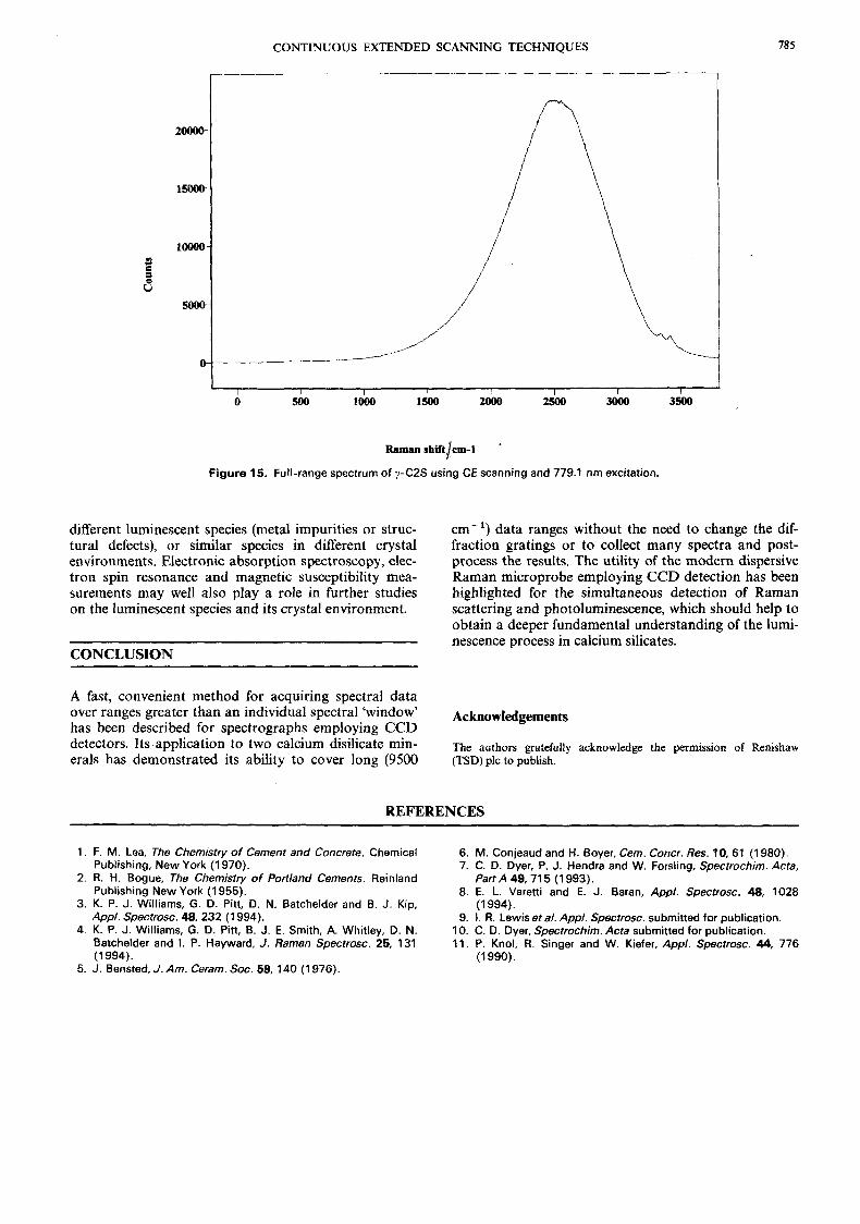
and in part to a fall in detector responsivity; in addi- The B-C2S spectrum (Fig. 15) again shows one set of the tion, an apparent increase in absolute background PL well resolved and highly structured PL bands at 1500 level is superimposed on the RS and gives a higher shot cm-l. However, the other, which should appear at noise contribution. The weak RS from pC2S is almost around 300 cm-', is masked by the rising edge of the obliterated by the PL background (Fig. 14); however, Rayleigh filter profile. This is further confused by the two bands visible in the static spectrum (Fig. 6) were periodic fluctuations in the Rayleigh filter transmission still in evidence at SNR 2-3 : 1 after scale expansion. and superimposition with the RS. In the case of the two
/ L 0 2000 4Ooo 6doo sdoo
Raman shift /cm-1
Figure 12. Full-range spectrum of B-CZS using CE scanning and 514.5 nm excitation.

784 C. DYER AND B. J. E. SMITH
0 uioo 4doo & sdoo
Raman Shiftbm-1
Figure 13. Full-range spectrum of yC2S using CE scanning and 514.5 nm excitation.
disilicates studied here, the spectral separation of the RS and PL in the 514.5 nm-excited spectrum is more useful than the strongly overlapped and partially attenuated 779.1 nm-excited spectrum.
It should be noted that all of the spectra are strongly affected by a fall-off in detector performance past 900 nm. The long-wavelength limit is determined strongly by the CCD detector response. This is affected by the bandgap of the silicon at the operating temperature of the device, and limits the useful range of the CCD to below lo00 nm. Between 900 and 10oO nm, the sensi-
tivity of the device drops by an order of magnitude. Since this fall-off amounts to an order of magnitude in spectral sensitivity, it implies that the y-C2S NIR- excited luminescence, which appears to be falling beyond ca. 2500 cm-’, is actually still increasing towards longer wavelength. This agrees well with FT- Raman studies.’-’ O
One area of debate highlighted by both 514.5 and 779.1 nm excitation will undoubtedly be why the j?-C2S species’ PL exhibits so much structure, whereas the y-C2S species only gives a broad band. This may reflect
6000
4Ooo
4 ’ 2000 6
0
I I I I I I I I 0 500 I000 1500 2000 2500 3Ooo 3500
Raman shift/em-1
Figure 14. Full-range spectrum of B-CZS using CE scanning and 779.1 nm excitation.
CONTINUOUS EXTENDED SCANNING TECHNIQUES
2oooo-
fS000-
1oooO-
5Ooo-
0
785
I I 1 I I I I I
Raman shiftbem-1 . Figure 15. Full-range spectrum of y-C2S using CE scanning and 779.1 nm excitation.
different luminescent species (metal impurities or struc- cm-') data ranges without the need to change the dif- tural defects), or similar species in different crystal fraction gratings or to collect many spectra and post- environments. Electronic absorption spectroscopy, elec- process the results. The utility of the modern dispersive tron spin resonance and magnetic susceptibility mea- Raman microprobe employing CCD detection has been surements may well also play a role in further studies highlighted for the simultaneous detection of Raman on the luminescent species and its crystal environment. scattering and photoluminescence, which should help to
obtain a deeper fundamental understanding of the lumi- nescence process in calcium silicates.
CONCLUSION
A fast, convenient method for acquiring spectral data over ranges greater than an individual spectral 'window' has been described for spectrographs employing CCD detectors. Its application to two calcium disilicate min- erals has demonstrated its ability to cover long (9500
Acknow~edgements
The authors gratefully acknowledge the pemission of Renishaw (TSD) plc to publish.
REFERENCES
1. F. M. Lea, The Chemistry of Cement and Concrete. Chemical Publishing, New York (1970).
2. R . H. Bogue, The Chemistry of Portland Cements. Reinland Publishing New York (1955).
3. K. P. J. Williams, G. D. Pitt, D. N. Batchelder and B. J. Kip, Appl. Spectrosc. 48, 232 (1994).
4. K. P. J. Williams, G. D. Pitt, B. J. E. Smith, A. Whitley, D. N. Batchelder and I . P. Hayward, J. Raman Spectrosc. 25, 131 (1 994).
5. J. Bensted, J. Am. Ceram. SOC. 59, 140 (1 976).
6. M. Conjeaud and H. Boyer, Cem. Concr. Res. 10,61 (1980). 7. C. D. Dyer, P. J. Hendra and W. Forsling, Spectrochim. Acta,
8. E. L. Varetti and E. J. Baran, Appl. Spectrosc. 48, 1028
9. 1. R. Lewis eta/. Appl. Spectrosc. submitted for publication.
ParrA49.715 (1993).
( 1 994).
10. C. D. Dyer, Spectrochim. Acta submitted for publication. 11. P. Knol, R . Singer and W. Kiefer, Appl. Spectrosc. 44, 776
(1990).