application note an 20-003 - semikron
TRANSCRIPT

© by SEMIKRON / 2020-08-04 / Application Note PROMGT.1023/ Rev.7/ Template Application Note
Page 1/11
Field-Testing of Power Semiconductor Modules1. Purpose of Testing.....................................................................................................................1
1.1 Production testing at SEMIKRON ............................................................................................11.2 Incoming inspection at OEM ..................................................................................................21.3 Troubleshooting & “go/no-go” testing in field ...........................................................................2
2. Equipment................................................................................................................................22.1 Digital multimeter with diode check function ............................................................................2
2.1.1 Forward (conducting) direction ........................................................................................22.1.2 Reverse (blocking) direction ............................................................................................2
2.2 Ohmmeter ..........................................................................................................................2
3. Testing Diode/Thyristor Modules..................................................................................................33.1 Diode .................................................................................................................................33.2 Thyristor.............................................................................................................................43.3 Thyristor gate characteristics .................................................................................................4
4. Testing IGBT/MOSFET Modules....................................................................................................54.1 Forward and reverse characteristics........................................................................................64.2 Gate characteristics..............................................................................................................7
5. Testing IPMs and Gate Drivers ....................................................................................................75.1 Power base .........................................................................................................................75.2 Gate drivers ........................................................................................................................8
5.2.1 Bias current ..................................................................................................................85.2.2 Switching current...........................................................................................................95.2.3 Errors .........................................................................................................................10
6. Conclusion..............................................................................................................................10
1. Purpose of Testing
Power semiconductor modules may be subjected to multiple tests during their lifetimes. As the cost and complexity of testing can be high, it is important to consider why the device is being tested. Improper testing can lead one to reject a good part or worse, damage a good device.
1.1 Production testing at SEMIKRONEvery power semiconductor component is tested to ensure its proper functionality. Forward (conducting) and reverse (blocking) characteristics are tested using custom test equipment capable of supplying the rated current and voltage for the module (e.g. hundreds of amperes and thousands of volts). High voltage testing is also performed to ensure the integrity of the insulation system between “live” and “grounded” parts of the module (e.g. terminals and baseplate).
Application NoteAN 20-003
Revision: 00 Issue date: 2020-08-04Prepared by: Paul DrexhageApproved by: Ingo Rabl, Dr. Ulrich Nicolai
Keyword: testing, multimeter, DMM

© by SEMIKRON / 2020-08-04 / Application Note PROMGT.1023/ Rev.7/ Template Application Note
Page 2/11
1.2 Incoming inspection at OEMSome customers will attempt electrical testing of components as they arrive into the factory, prior to installation in equipment. This may have been instigated due to previous poor quality from a supplier or the perception that such screening will result in a lower failure rate for the finished product. Unfortunately, the testing is too often done with rudimentary low voltage equipment incapable of supplying the high voltage and currents for which the datasheet is valid. At best, this results in unnecessarily rejected parts and at worst, damage to the components. Far better is to address quality issues with the supplier and implement a production test process involving functional testing of the component in a subassembly.
1.3 Troubleshooting & “go/no-go” testing in fieldThe most common situation is that a piece of equipment has failed in the field and requires servicing. The power semiconductor components must be checked to determine if they need replacement or if the equipment is safe to re-start. A fast test using simple equipment is needed to determine whether the component is good (“go”) or bad (“no-go”). This is the focus of this document.
2. Equipment
2.1 Digital multimeter with diode check functionProper field-testing of a semiconductor requires a digital multimeter (DMM) equipped with a diode function. This function is indicated by the diode symbol on the selector wheel or via secondary pushbutton. The purpose of this test is to check that the diode blocks in one direction and conducts (with a small voltage drop) in the other direction.
2.1.1 Forward (conducting) directionThe diode check function works by applying a small forward voltage to turn the diode on and measures voltage drop across the diode with a small current. This measured voltage drop is not the same as the “threshold voltage” (e.g. VF0), listed on device datasheets, which is instead part of the straight-line approximation of the diode forward characteristics used for loss calculations. Furthermore, the measured voltage drop with power diodes is usually less than the expected 0.7V typical of small signal silicon diodes (e.g. 1N4148). Power diodes in 600V-1700V modules will typically give a reading from 0.2 to 0.5V.
2.1.2 Reverse (blocking) directionWhen the diode is reversed biased, the diode check function should report that the diode is in the blocking (off) state. This is typically indicated as “OL”, “out of range”, “open”, or similar. As the DMM is only able to supply a small voltage (e.g. the battery voltage: 9V) this test does not guarantee that the diode is capable of blocking its rated voltage (typically >600V for power semiconductors). Because of the uncertainty of measured values described above, the purpose of the diode check is to determine if the diode is completely shorted or completely open. Diodes that have gone short will read “0V” (or a very low voltage drop) in both directions whereas diodes that have gone open will read “OL” in both directions.
2.2 OhmmeterUsers will often try to use the ohmmeter to measure the resistance of semiconductors in order to determine their health. While a semiconductor that has failed open may read in the megaohm range and a shorted semiconductor may read in the milliohm range, any reading in-between will be inconsistent between devices for the following reasons: First, semiconductor devices are made up of differently doped silicon areas (“P type” and “N type”) which are combined to form PN junctions. The P- and N-doped areas are not homogenous but exhibit gradients ("doping profiles"). These doping profiles are an important part of the device design and are a major factor in achieving the desired electrical properties. In power semiconductors, the major PN junctions are designed to operate with hundreds (or thousands) of volts across them. The voltage (e.g. 9V) supplied by a DMM is too low to create a fully extended electric field across the junction and at the termination structure (area that lowers the electric fields at the edge of the chip). This means that the ohmmeter is only measuring a limited part of the doping profile and the reading does not reflect the device properties at operational conditions. Moreover, as the PN junction does not exhibit ohmic (i.e. linear I-V) behavior, a supply voltage variation might lead to different results. In power modules, the series resistance of the terminals leads to further variation.
© by SEMIKRON / 2020-08-04 / Application Note PROMGT.1023/ Rev.7/ Template Application Note
Page 3/11
Second, in order to allow for measuring resistors in-circuit some digital ohmmeters use a very low voltage (e.g. <0.6VDC) to avoid forward biasing other diodes or transistors that may be in parallel with the resistor being measured. This means that if the ohmmeter function is used to measure a diode directly, the user will likely get a false open reading as the meter is not supplying enough voltage to bias the diode into an on-state.
There are some instances when the ohmmeter is useful for evaluating basic behavior (e.g. charging an IGBT/MOSFET gate, section 4.2), but exact resistance values are not used.
High voltage resistance meters (e.g. “meggers”, megohmmeters) are intended for checking the quality of insulation and can potentially damage semiconductors.
3. Testing Diode/Thyristor Modules
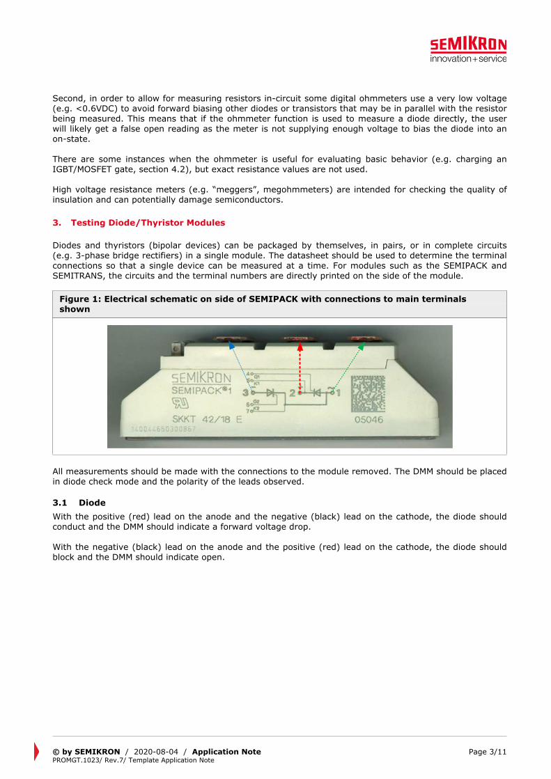
Diodes and thyristors (bipolar devices) can be packaged by themselves, in pairs, or in complete circuits (e.g. 3-phase bridge rectifiers) in a single module. The datasheet should be used to determine the terminal connections so that a single device can be measured at a time. For modules such as the SEMIPACK and SEMITRANS, the circuits and the terminal numbers are directly printed on the side of the module.
Figure 1: Electrical schematic on side of SEMIPACK with connections to main terminals shown
All measurements should be made with the connections to the module removed. The DMM should be placed in diode check mode and the polarity of the leads observed.
3.1 DiodeWith the positive (red) lead on the anode and the negative (black) lead on the cathode, the diode should conduct and the DMM should indicate a forward voltage drop.
With the negative (black) lead on the anode and the positive (red) lead on the cathode, the diode should block and the DMM should indicate open.

© by SEMIKRON / 2020-08-04 / Application Note PROMGT.1023/ Rev.7/ Template Application Note
Page 4/11
Figure 2: Typical forward (L) and reverse (R) measurements for a “good” diode
0.2~0.5V
COM V
A K
OL
COM V
AK
3.2 ThyristorThe gate of the thyristor should be left unconnected during testing.
With the positive (red) lead on the anode and the negative (black) lead on the cathode, the thyristor should block and the DMM should indicate open.
With the negative (black) lead on the anode and the positive (red) lead on the cathode, the thyristor should block and the DMM should indicate open.
Figure 3: Typical forward (L) and reverse (R) measurements for a “good” thyristor
OL
COM V
A KG
OL
COM V
AKG
3.3 Thyristor gate characteristicsThe gate-cathode of an ideal thyristor is a PN junction. In many thyristors, there is also a parallel “short circuit” path between gate and anode. This path is designed to provide a large initial current to help fire the device. Because this path is made from uniform p-doped silicon, there is typically a measureable resistance of 10~50Ω between gate and cathode. However, this resistance value is not characterized by the manufacturer and this value is given only to inform the user that a low resistance here does not indicate a damaged device. When measured with the diode check, the gate-cathode connection will appear as a low (but nonzero) voltage drop (e.g. 0.01~0.05V) in both directions.

© by SEMIKRON / 2020-08-04 / Application Note PROMGT.1023/ Rev.7/ Template Application Note
Page 5/11
Figure 4: Measured "resistance" between gate and cathode in a thyristor
4. Testing IGBT/MOSFET Modules
IGBTs and MOSFETs are active devices that require an external gate voltage to turn them on so the on-state voltage drop cannot be directly measured with the diode function of the DMM. However, IGBTs devices are usually co-packaged with a freewheeling (inverse) diode that can be checked. MOSFETs have an intrinsic body diode that can be measured and, in the case of silicon carbide (SiC) MOSFETs, they may have an additional freewheeling diode in parallel.
Figure 5: Terminals and diode locations for IGBTs and MOSFETs
Like the bipolar modules, IGBT/MOSFET modules also have the schematic printed on the side and can help determine on which terminals to place the meter leads (Figure 6).

© by SEMIKRON / 2020-08-04 / Application Note PROMGT.1023/ Rev.7/ Template Application Note
Page 6/11
Figure 6: Electrical schematic on side of SEMITRANS 3 with connections to main terminals shown
Other modules may have two terminals internally connected to the same point, such as the AC terminals on the SEMiX housing (Figure 7). Auxiliary connections (emitter or cathode) may be duplicated on smaller terminals for connections to a driver.
Figure 7: Electrical schematic on side of SEMiX 3s with connections to main terminals shown
4.1 Forward and reverse characteristicsAll measurements should be made with the connections to the module removed. The DMM should be placed in diode check mode and the polarity of the leads observed.
With the positive (red) lead on the collector (C) and the negative (black) lead on the emitter, the DMM should read open.
With the positive (red) lead on the emitter (E) and the negative (black) lead on the collector (C), the diode should conduct and the DMM should indicate a forward voltage drop.

© by SEMIKRON / 2020-08-04 / Application Note PROMGT.1023/ Rev.7/ Template Application Note
Page 7/11
Figure 8: Typical forward (L) and reverse (R) measurements for a “good” IGBT
OL
COM V
E/A
G
C/K0.2~0.5V
COM V
E/A
G
C/K
4.2 Gate characteristicsThe gate-emitter (gate-source) junction of an IGBT (MOSFET) behaves like a capacitor due to its insulated construction. For this, the ohmmeter setting of the DMM can be used but only for the purposes of charging the gate and not to look for a specific resistance reading.
The oxide layer that makes up the insulation the gate structure is very thin and thus susceptible to electrostatic discharge (ESD). Care should be taken not to touch the gate without proper ESD precautions.
All measurements should be made with the connections to the module removed. The DMM should be placed in ohmmeter mode.
With the positive or negative lead on the gate and the other lead on the emitter (source), the meter should show a quickly increasing resistance that goes above the megaohm range. Most meters should indicate out-of-range (OL). This shows the meter charging up the capacitance the “resistance” being shown is the V / I characteristic. As the current decreases as the capacitor charges up, the resistance goes to infinity.
A damaged gate will typically show a dead short (e.g. 0Ω) to the emitter (source) or collector (drain).
5. Testing IPMs and Gate Drivers
Intelligent Power Modules (IPM) contain multiple IGBTs in the “power base” along with a driver (and heatsink, in the case of the SKiiP). Checking the IGBTs in an IPM is similar to discrete modules, though first the circuit topology and driver connection must be determined. Additional components on the driver board in parallel with the IGBTs may give misleading results.
5.1 Power baseFor an IPM such as the SKiiP, the power base consists of multiple “bays” each containing an IGBT half bridge. Depending on the SKiiP type, these bays may be operated individually (GD type) or in parallel (GB type). In the GB type, since the paralleling of the power terminals is done externally (using busbars), each bay must be checked separately.

© by SEMIKRON / 2020-08-04 / Application Note PROMGT.1023/ Rev.7/ Template Application Note
Page 8/11
Figure 9: Checking the TOP free-wheeling diode in the first bay of a three-bay SKiiP. Note that individual bays are not connected to each other at the power terminals
0.2~0.4V
COM V
+
-
+
-
+
-
A
K
5.2 Gate driversDue to their complex circuits, gate drivers cannot be easily checked to determine which individual components have malfunctioned. Fortunately, for IPMs and discrete driver cores it has been determined that the current drawn from the power supply is usually a good indicator for whether the gate driver is “good” or “bad”. Two types of current draw can be checked: the non-switching (quiescent) current and the current while the IGBTs are switching.
This process requires a regulated power supply, an ammeter for measuring current from the supply, and a method of applying a complementary TOP/BOT gating signal at a fixed gating frequency. It is recommended that dedicated test equipment be assembled if testing is done regularly or in high quantity. Certain companies manufacture equipment integrating power supply, gating signals, and measurement points in a portable package [3].
The input pins of driver circuits may also be susceptible to electrostatic discharge (ESD). Care should be taken not to handle driver circuit boards without proper ESD precautions.
5.2.1 Bias currentThe supply current without switching can be found on the device datasheet (Figure 10) for a given input voltage (e.g. IS0).

© by SEMIKRON / 2020-08-04 / Application Note PROMGT.1023/ Rev.7/ Template Application Note
Page 9/11
Figure 10: Exemplary value of bias current (from SKiiP datasheet)
This bias current can be checked by applying a regulated (benchtop) power supply with an ammeter in series (Figure 11) and checking the current drawn by the driver when it is in its standby state. High voltage (e.g. DC link voltage) should not be applied.
Figure 11: Connections for measuring driver bias current
+- Vs
IS0
A
DR
IVER
5.2.2 Switching currentAlso given on the driver datasheet (Figure 12) is the supply current drawn when the gate driver is switching (e.g. Is). In the case of IPMs, this value may also include current drawn by current sensors so the expected current must be calculated using a formula.
Figure 12: Exemplary value of switching current (from SKiiP datasheet)
Again, a regulated DC supply with ammeter is applied. Additionally, an on-off (square wave) gating signal is needed for the top and bottom switches. Top and bottom switches are gated complementarily at a fixed switching frequency. The duty cycle is irrelevant.
Figure 13: Connections for measuring switching current
TOP BOT+- Vs
ISA
DR
IVER

© by SEMIKRON / 2020-08-04 / Application Note PROMGT.1023/ Rev.7/ Template Application Note
Page 10/11
Using the example values from Figure 12, with only 24VDC control power applied and a 10kHz gating signal, a current draw of 530mA should be expected. If the IPM does not switch at all, only the 240mA bias current would be drawn. If only one IGBT (TOP or BOT) was switching, a value between 240mA and 530mA would be expected.
5.2.3 ErrorsAs part of any troubleshooting, the driver should be checked to determine if any error signals are being generated. Generally, a driver connected to an IGBT module with only control power applied should not be generating any error signals (e.g. undervoltage, DESAT, etc.). However, since drivers do not often have the ability to self-diagnosis problems, it is possible that a driver could be malfunctioning and not indicate an error.
6. Conclusion
Power semiconductors are complex devices that cannot be fully evaluated without specialized equipment. However, a digital multimeter with the diode check function allows for a quick “go/no-go” check that covers the majority of failure modes in the field.

© by SEMIKRON / 2020-08-04 / Application Note PROMGT.1023/ Rev.7/ Template Application Note
Page 11/11
Figure 1: Electrical schematic on side of SEMIPACK with connections to main terminals shown..................3Figure 2: Typical forward (L) and reverse (R) measurements for a “good” diode......................................4Figure 3: Typical forward (L) and reverse (R) measurements for a “good” thyristor .................................4Figure 4: Measured "resistance" between gate and cathode in a thyristor...............................................5Figure 5: Terminals and diode locations for IGBTs and MOSFETs ...........................................................5Figure 6: Electrical schematic on side of SEMITRANS 3 with connections to main terminals shown.............6Figure 7: Electrical schematic on side of SEMiX 3s with connections to main terminals shown ...................6Figure 8: Typical forward (L) and reverse (R) measurements for a “good” IGBT ......................................7Figure 9: Checking the TOP free-wheeling diode in the first bay of a three-bay SKiiP. Note that individual bays are not connected to each other at the power terminals ...............................................................8Figure 10: Exemplary value of bias current (from SKiiP datasheet)........................................................9Figure 11: Connections for measuring driver bias current.....................................................................9Figure 12: Exemplary value of switching current (from SKiiP datasheet) ................................................9Figure 13: Connections for measuring switching current ......................................................................9
References[1] www.SEMIKRON.com[2] A. Wintrich, U. Nicolai, W. Tursky, T. Reimann, “Application Manual Power Semiconductors”, 2nd
edition, ISLE Verlag 2015, ISBN 978-3-938843-83-3[3] Ingenieurbüro Billmann. Lerchensteige 10, 91448 Emskirchen, Germany. www.ib-billmann.de
IMPORTANT INFORMATION AND WARNINGSThe information in this document may not be considered as guarantee or assurance of product characteristics ("Beschaffenheitsgarantie"). This document describes only the usual characteristics of products to be expected in typical applications, which may still vary depending on the specific application. Therefore, products must be tested for the respective application in advance. Application adjustments may be necessary. The user of SEMIKRON products is responsible for the safety of their applications embedding SEMIKRON products and must take adequate safety measures to prevent the applications from causing a physical injury, fire or other problem if any of SEMIKRON products become faulty. The user is responsible to make sure that the application design is compliant with all applicable laws, regulations, norms and standards. Except as otherwise explicitly approved by SEMIKRON in a written document signed by authorized representatives of SEMIKRON, SEMIKRON products may not be used in any applications where a failure of the product or any consequences of the use thereof can reasonably be expected to result in personal injury. No representation or warranty is given and no liability is assumed with respect to the accuracy, completeness and/or use of any information herein, including without limitation, warranties of non-infringement of intellectual property rights of any third party. SEMIKRON does not assume any liability arising out of the applications or use of any product; neither does it convey any license under its patent rights, copyrights, trade secrets or other intellectual property rights, nor the rights of others. SEMIKRON makes no representation or warranty of non-infringement or alleged non-infringement of intellectual property rights of any third party which may arise from applications. This document supersedes and replaces all information previously supplied and may be superseded by updates. SEMIKRON reserves the right to make changes.
SEMIKRON INTERNATIONAL GmbHSigmundstrasse 200, 90431 Nuremberg, GermanyTel: +49 911 6559 6663, Fax: +49 911 6559 [email protected], www.semikron.com