application hints tja1055t - nxp semiconductors hints tja1055t fault-tolerant can transceiver rev....
TRANSCRIPT

Application Hints TJA1055T Fault-tolerant CAN transceiver Rev. 1.5 — 25 Feb 2016 Application Hints
Document information
Info Content
Title TJA1055T - Fault-tolerant CAN transceiver
Author(s) Frank Schade / Matthias Muth
Department Systems & Application; Product Line CAN/LIN
Keywords TJA1055T, TJA1055T/3, TJA1054T, TJA1054AT, Controller Area Network (CAN), Transceiver, Physical Layer, Fault Tolerant, Low Speed
NXP Semiconductors Application Hints TJA1055T Automotive Innovation Center
AH0801 © NXP B.V. 2016. All rights reserved.
Application Hints Rev. 1.5 — 25 Feb 2016 2 of 86
Contact information For additional information, please visit: http://www.nxp.com For sales office addresses, please send an email to: [email protected]
Summary
The TJA1055T is an advanced fault-tolerant CAN transceiver primarily intended for low-speed applications up to 125kBd in passenger cars. Besides the differential receive and transmit capability the transceiver provides single-wire transmitter and/or receiver in error conditions. The TJA1055T is the enhanced successor of the fault-tolerant CAN transceivers TJA1054T and TJA1054TA with the same functionality but offering in addition a number of improvements.
These application hints provide information on how to use the TJA1055T in CAN applications
Revision history
Rev Date Description
1.0 2007-02-01 Initial version
1.1 2008-03-06 - Editorial changes - 4.2.4 subchapters introduced and example calculation of RXD / ERR_N pull-up resistors added - 5.1.3 Go-to Sleep procedure clarified - 7 Design checklist updated with item 20
1.2 2008-06-06 - Timing picture in Fig 21 updated
1.3 2011-05-02 - Table 3 Static characteristics of input pins STB_N, EN and TXD in chapter 2.5 added - Chapter 4.2.7.1 updated - Chapter 4.2.7.5 updated
1.4 2011-07-08 - Legal page updated
1.5 2016-02-25 - Added details on RXD / ERR_N pin behavior at very low BAT supply conditions, see chapter 4.2.4.3 and the according check list in chapter 7. - Added a recommendation for the ERR_N handling in chapter 5.2.3. and check list in chapter 7.

NXP Semiconductors Application Hints TJA1055T Automotive Innovation Center
AH0801 © NXP B.V. 2016. All rights reserved.
Application Hints Rev. 1.5 — 25 Feb 2016 3 of 86
Contact information For additional information, please visit: http://www.nxp.com For sales office addresses, please send an email to: [email protected]
continued >>
NXP Semiconductors Application Hints TJA1055T Automotive Innovation Center
AH0801 © NXP B.V. 2016. All rights reserved.
Application Hints Rev. 1.5 — 25 Feb 2016 4 of 86
Contents
1. Introduction ........................................................................................................................................................ 7
2. Overview and General Description ................................................................................................................... 8 2.1 Pinning ................................................................................................................................................................. 8 2.2 Fail Safe ............................................................................................................................................................. 10 2.3 Block Diagram .................................................................................................................................................... 12 2.4 Typical Application ............................................................................................................................................. 13 2.5 Main Differences between TJA1054T and TJA1055T ........................................................................................ 14
3. Fault-tolerant Physical Layer .......................................................................................................................... 16 3.1 The FT-CAN Principle ........................................................................................................................................ 16 3.2 Network Architectures ........................................................................................................................................ 17 3.3 Bus Level Scheme ............................................................................................................................................. 17
4. Hardware Design .............................................................................................................................................. 19 4.1 Application Diagram 3V and 5V ......................................................................................................................... 19 4.2 Application Details .............................................................................................................................................. 21 4.2.1 INH Circuit Example ..................................................................................................................................... 21 4.2.2 Wake_N Pin Circuit ...................................................................................................................................... 22 4.2.3 CAN Bus Circuit............................................................................................................................................ 25 4.2.4 µC- Transceiver Interface ............................................................................................................................. 26 4.2.4.1 Mode Pins EN and STB_N ..................................................................................................................... 26 4.2.4.2 Pins TXD, RXD and ERR_N ................................................................................................................... 26 4.2.4.3 Application details for RXD and ERR_N circuitry .................................................................................... 27 4.2.4.4 Minimum Pull-up Resistor for RXD and ERR_N for TJA1055T/3 ............................................................ 27 4.2.4.5 Usage of Series Resistors REMC ........................................................................................................... 28 4.2.5 BAT and VCC Supply Circuit ........................................................................................................................ 28 4.2.6 Current Consumption on BAT Pin ................................................................................................................ 30 4.2.7 Current Consumption on VCC Pin ................................................................................................................ 31 4.2.7.1 Average Supply Current; no Bus Short-Circuit Conditions ...................................................................... 33 4.2.7.2 Worst Case Max VCC Supply; with a Dual Short Circuit ......................................................................... 35 4.2.7.3 VCC extra supply current in dual fault condition ..................................................................................... 36 4.2.7.4 Calculation of worst-case bypass capacitor ............................................................................................ 36 4.3 Application Example: Wake-up via RXD / ERR_N without VCC ........................................................................ 37 4.3.1 Application Description ................................................................................................................................. 38 4.3.2 Wake-up capability of the TJA1055T with VCC off ....................................................................................... 38
5. Software Design ............................................................................................................................................... 39 5.1 Operation Mode Control ..................................................................................................................................... 39 5.1.1 Overview ...................................................................................................................................................... 39 5.1.2 Normal Mode (‘1’ ‘1’) .................................................................................................................................... 40 5.1.3 Low-power Mode: Go-to-Sleep (‘0’ ‘1’) ......................................................................................................... 40 5.1.4 Low-power Mode: Standby / Sleep (‘0’ ‘0’) ................................................................................................... 42 5.1.5 Low-power Mode: Power-on Standby (‘1’ ‘0’) ............................................................................................... 43 5.1.6 State Diagram............................................................................................................................................... 45 5.2 Internal Flag Signaling ....................................................................................................................................... 46 5.2.1 Power-on Flag .............................................................................................................................................. 46 5.2.2 Wake-up Flag ............................................................................................................................................... 46 5.2.3 Error-Flag ..................................................................................................................................................... 47 5.2.4 INH / RXD / ERR_N Pin Behaviour and Flag Signalling ............................................................................... 47 5.3 System Wake-up ................................................................................................................................................ 49

NXP Semiconductors Application Hints TJA1055T Automotive Innovation Center
Please be aware that important notices concerning this document and the product(s) described herein, have been included in the section 'Legal information'.
© NXP Semiconductors 2016. All rights reserved.
For more information, please visit: http://www.nxp.com For sales office addresses, email to: [email protected]
Date of release: 25 Feb 2016 Document identifier: AH0801
5.3.1 Wake-up Overview ....................................................................................................................................... 49 5.3.2 Local wake-up .............................................................................................................................................. 49 5.3.3 Remote wake-up .......................................................................................................................................... 49 5.3.4 Host Wake-up (Mode change) ...................................................................................................................... 50 5.4 Flow Charts ........................................................................................................................................................ 51 5.4.1 Example: ECU Cold Start ............................................................................................................................. 51 5.4.2 Start-up from Standby Mode ........................................................................................................................ 52 5.4.3 Example: How to enter Standby Mode ......................................................................................................... 52 5.4.4 Example: How to enter Sleep Mode ............................................................................................................. 53
6. EMC and ESD ................................................................................................................................................... 55 6.1 EMI and EME improvements ............................................................................................................................. 55 6.1.1 Series resistors in TXD and RXD for EME improvement .............................................................................. 55 6.1.2 Common mode choke for improvements of RF-immunity ............................................................................. 55 6.1.3 Bus capacitors for EMI improvements .......................................................................................................... 56 6.2 ESD protection with PESD1CAN ....................................................................................................................... 57
7. Design Check List ............................................................................................................................................ 58
8. FAQs ................................................................................................................................................................. 60 8.1 There was a wake-up event during the “Goto Sleep” procedure. ....................................................................... 60 8.2 System operates in Single Wire Mode all time ................................................................................................... 60 8.3 System does not wake-up, even if there is bus activity ...................................................................................... 60 8.4 Transceiver is damaged when external tools are connected ............................................................................. 60 8.5 CAN tool cannot communicate with certain application ...................................................................................... 61
9. Appendix ........................................................................................................................................................... 62 9.1 Bus Termination ................................................................................................................................................. 62 9.1.1 Dimensioning of the bus termination resistors .............................................................................................. 62 9.1.1.1 Variable System Size and Optional Nodes ............................................................................................. 62 9.1.1.2 Distribution of the termination resistors ................................................................................................... 63 9.1.2 Tolerances of Bus Termination Resistors ..................................................................................................... 63 9.1.3 Power Dissipation of Termination Resistors ................................................................................................. 65 9.1.3.1 Summary ................................................................................................................................................ 65 9.1.3.2 Average power dissipation, no bus failures ............................................................................................. 65 9.1.3.3 Maximum continuous power dissipation (single bus failure) ................................................................... 65 9.1.3.4 Maximum peak power dissipation (single bus failure) ............................................................................. 65 9.2 Bus Failure Management ................................................................................................................................... 67 9.2.1 Overview of transceiver state in Normal Mode ............................................................................................. 67 9.2.2 Failure overview and description .................................................................................................................. 68 9.3 Pin FMEA ........................................................................................................................................................... 73 9.4 Ground Shift ....................................................................................................................................................... 79 9.4.1 GND shift definitions ..................................................................................................................................... 79 9.4.2 GND shift limitations ..................................................................................................................................... 79 9.4.3 CANH interruption ........................................................................................................................................ 80 9.4.4 CANL interruption ......................................................................................................................................... 80 9.4.5 CANH shorted to BAT or VCC ...................................................................................................................... 80 9.4.6 CANH shorted to GND ................................................................................................................................. 81 9.4.7 CANL shorted to GND or BAT ...................................................................................................................... 81 9.4.8 CANL shorted to VCC .................................................................................................................................. 81 9.4.9 Short between CANH and CANL .................................................................................................................. 82
10. Quick Reference ............................................................................................................................................... 83
11. References ........................................................................................................................................................ 84
NXP Semiconductors Application Hints TJA1055T Automotive Innovation Center
Please be aware that important notices concerning this document and the product(s) described herein, have been included in the section 'Legal information'.
© NXP Semiconductors 2016. All rights reserved.
For more information, please visit: http://www.nxp.com For sales office addresses, email to: [email protected]
Date of release: 25 Feb 2016 Document identifier: AH0801
12. Legal information ............................................................................................................................................. 85 12.1 Definitions .......................................................................................................................................................... 85 12.2 Disclaimers ........................................................................................................................................................ 85 12.3 Trademarks ........................................................................................................................................................ 85

NXP Semiconductors Application Hints TJA1055T Automotive Innovation Center
AH0801 © NXP B.V. 2016. All rights reserved.
Application Hints Rev. 1.5 — 25 Feb 2016 7 of 86
1. Introduction The fault-tolerant CAN transceiver TJA1055T from NXP Semiconductors provides the physical link between the protocol controller and the physical bus wires in a Controller Area Network (CAN). Additionally the transceiver is able to control one or more external voltage regulators within an Electronic Control Unit (ECU) and supports an advanced low power management to reduce the current consumption significantly. This allows the TJA1055T to enter Sleep Mode and as a result to switch off the external voltage regulators in order to deactivate the VCC supply of the transceiver and the host microcontroller. The TJA1055T has been developed mainly for low-speed CAN applications (up to 125 kBd) in passenger cars; especially for comfort electronics (see Fig 1). The device operates in differential mode but will switch to a single-wire transmitter and/or receiver in error conditions. The bus is continuously monitored to switch back to normal operating mode when faults disappear. In the supported failure cases all nodes continue to communicate.
Fig 1. Target Applications for Fault-tolerant CAN Network
The TJA1055T is offered in two versions with different voltage interfaces towards the microcontroller. The TJA1055T is dedicated for microcontrollers with a 5V interface and the TJA1055T/3 is dedicated for microcontrollers with a 3V or 3.3V interface.
Compared to the TJA1054T(A) the TJA1055T is improved with respect to current consumption and EMC capability. Furthermore the TJA1055T is suitable to replace the TJA1054T(A) one-to-one in existing applications, if desired. The TJA1055T is the successor of the so-called “golden device” TJA1054T and thus, fully compatible with the ISO 11898-3 standard [1].
Seat
Roof
Door
Climate
Steering Wheel
Trunk

NXP Semiconductors Application Hints TJA1055T Automotive Innovation Center
AH0801 © NXP B.V. 2016. All rights reserved.
Application Hints Rev. 1.5 — 25 Feb 2016 8 of 86
2. Overview and General Description
2.1 Pinning
Fig 2. Pinning diagram of the TJA1055T
Pin INH
The intention of the output pin inhibit (INH) is to control one or more voltage regulators within the ECU. Details can be found in chapter 4.2.1.
In Sleep Mode the INH pin gets floating. Due to the typical pull-down behaviour of inhibit input pins of common voltage regulators, this results in disabling the according voltage regulator and thus in disabling the VCC supply voltage of the microcontroller and the transceiver.
On any wake-up request to the TJA1055T or after a battery power-on the INH pin is pulled to the battery voltage, thus enabling the external voltage regulator. In case the INH pin is not of use, it can be left open.
Pin TXD
The TXD pin is the transmit data input pin. The transceiver receives the digital bit stream from the CAN controller to be transmitted to the CAN bus lines via pin TXD. A logical LOW level represents the dominant bus stage while a HIGH level represents the recessive bus state.
Pin RXD
The RXD pin is the receive data output for reading out the data from the bus lines. The analog bit stream received from the bus is transferred via RXD to the CAN-controller for further processing. When using a 5V microcontroller interface and a 5V transceiver this pin could be connected to the microcontroller directly. When using a 3V interface and the 3V version of the TJA1055T (TJA1055T/3) the RXD pin has additionally to be connected to VCC of the microcontroller via pull-up resistor.
8
9
10
7
6
5
INH 14
13
12
11
1
2
3
4
TXD
RXD
ERR
BAT
GND
CANL
CANH
STB
EN
WAKE
VCC
RTL
RTH
TJA1055T TJA1055T/3

NXP Semiconductors Application Hints TJA1055T Automotive Innovation Center
AH0801 © NXP B.V. 2016. All rights reserved.
Application Hints Rev. 1.5 — 25 Feb 2016 9 of 86
Pin ERR_N
The ERR_N (Error Not) pin is used to indicate an error, a wake-up or a power-on flag. When using a 5V microcontroller interface and a 5V transceiver this pin could be connected to the microcontroller directly. When using a 3V interface and the 3V version of the TJA1055T (TJA1055T/3) the ERR_N pin has additionally to be connected to VCC of the microcontroller via pull-up resistor.
Depending on the operating mode, different flags are reflected at pin ERR_N. These flags are signals with an active LOW behavior. In standby mode (EN = 0, STB_N = 0) the pin reflects the wake-up flag. In power-on standby mode (EN = 0, STB_N = 1) the power-on flag is signalled and in normal mode (EN = 1, STB_N = 1) the pin ERR_N indicates a bus failure condition.
Pin STB_N
STB_N (STB Not) is one of the two mode control pins of the transceiver. STB_N is the standby digital control signal. This active-low input pin is used together with the signal on pin EN to define the operation mode of the transceiver. This pin should directly connect to an output port pin of a microcontroller and provides an internal pull-down current source.
Pins EN
EN is the enable digital control signal. This input pin is used together with the signal on pin STB_N to define the operation mode of the transceiver. This pin should directly connect to an output port pin of a microcontroller and provides an internal pull-down current source.
Pin WAKE_N
The local wake-up pin (WAKE_N) is an input pin with internal pull-up to battery voltage. This pin is used for local wake-up. If WAKE_N detects a rising or falling edge, a wake-up condition is detected after a defined filter time (tWAKE). The wake-up event has higher priority than the go-to-sleep command.
RTH and RTL pin description
The pins RTH and RTL are the termination resistor connections of CANH and CANL. In case of a CANH bus wire error the CANH line is terminated via RTH with higher impedance compared to failure-free operation. In case of a CANL bus wire error the CANL line is terminated via RTL with higher impedance compared to the failure-free operation. The value of the external termination resistors should be between 500Ohm and 6kOhm. The overall resistor in the whole CAN network should be about 100Ohm per line. For further information and calculation of this resistor see chapter 9.1.
CANH and CANL pin description
The transceiver is connected to the bus via pins CANH and CANL. CANL is the LOW-level CAN bus line. In normal operating mode, the value of dominant state is about 1,4V and the value of recessive state is 5V. In low-power modes, the voltage of CANL is equal to battery voltage (see also Fig 7).
CANH is the HIGH-level CAN bus line. In normal operating mode, the value of dominant state is about 3,6V and the value of recessive state as well as in low-power modes is about 0V. These pins have a high robustness with a maximum voltage of ±58V and an ESD protection of ±8kV human body model.

NXP Semiconductors Application Hints TJA1055T Automotive Innovation Center
AH0801 © NXP B.V. 2016. All rights reserved.
Application Hints Rev. 1.5 — 25 Feb 2016 10 of 86
Pin VCC
The VCC supply provides the current needed for the transmitter and receiver of the TJA1055T during normal operation. The VCC supply must be designed with respect to the worst-case current consumption requirements (see chapter 4.2.7).
Pin GND
The pin GND is the ground pin and the reference value of all voltage in the transceiver. It is important to guarantee a well-defined GND connection between all ground pins within the ECU. This is important to guarantee optimum EMC behaviour of the overall system. Besides the GND connection to the outside world (cable tree) it is important to provide a good GND connection between the transceiver and the microcontroller. This is needed to keep the communication interface between microcontroller and transceiver unaffected by strong EMC injections into the bus cables.
Pin BAT
BAT is the battery supply pin of the transceiver. The battery supply ensures the local and remote wake-up capability of the TJA1055T when the VCC supply is switched off during Sleep Mode. The current consumption at pin BAT is very low and mainly supplying the digital circuitry as well as the wake-up components.
2.2 Fail Safe The TJA1055T provides several fail-safe features to protect the local hardware and the external bus system from being disturbed. This guarantees that the vehicles CAN communication keeps ongoing in case of local ECU faults. The main safety features are shown in Fig 3.
Fig 3. Overview of TJA1055T Fail-Safe features
BATGND
CANHCANL
TXD
STBEN
High impedance in case:Loss of Power
Bus system keeps unaffected incase of interrupted power supply
Over temperature protection
Destruction of bus pins avoided
TXD input monitoring
Continuous dominant clampingby CAN controller is interrupted
Fail-safe encoded control ports
Passive behaviour on portdisconnection
Input port mask out
Low VCC forces passivebehaviour of the transceiver
VCC
TJA1055

NXP Semiconductors Application Hints TJA1055T Automotive Innovation Center
AH0801 © NXP B.V. 2016. All rights reserved.
Application Hints Rev. 1.5 — 25 Feb 2016 11 of 86
The transceiver becomes passive and keeps the bus unaffected if the transceiver loses the power connection. This is achieved by switching the pins CANH, CANL, RTH and RTL to a high impedance state.
In case the connections to the mode control pins STB_N and/or EN are interrupted an internal pull-down source sets these input pins to LOW. This makes sure that the transceiver enters a low-power mode. Besides this, the mode control of the transceiver is coded digitally in such a way that glitches on pins STB_N and/or EN during any mode change do not lead to an unwanted operation mode change. Upon loss of the VCC supply the TJA1055T enters standby mode.
To avoid a continuous dominant clamped bus due to a clamped TXD pin a dedicated TXD dominant timeout function is provided. So, the bus cannot be permanently blocked by a single local failure.
In order to protect the transceiver from being damaged by over temperature, an according monitoring circuitry shuts down the CAN drivers until the temperature of the IC has cooled down again. Besides this, the voltage robustness on the bus pins is further increased to ±58V for the TJA1055T compared to the TJA1054T (-27V up to +40V).
NXP Semiconductors Application Hints TJA1055T Automotive Innovation Center
AH0801 © NXP B.V. 2016. All rights reserved.
Application Hints Rev. 1.5 — 25 Feb 2016 12 of 86
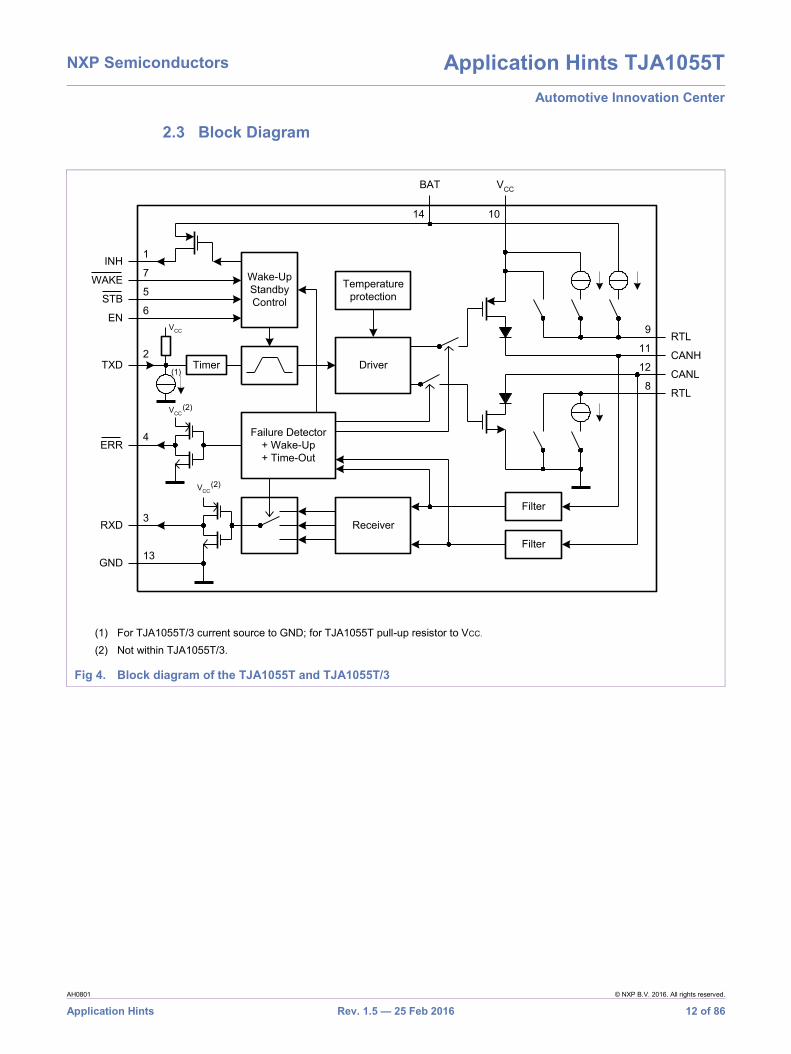
2.3 Block Diagram
(1) For TJA1055T/3 current source to GND; for TJA1055T pull-up resistor to VCC. (2) Not within TJA1055T/3.
Fig 4. Block diagram of the TJA1055T and TJA1055T/3
BAT
RTL9
VCC
11CANH
12
8CANL
RTL
Filter
Filter
1014
Driver
Failure Detector+ Wake-Up+ Time-Out
Temperatureprotection
Receiver
Wake-UpStandbyControl
Timer
GND13
VCC
VCC
VCC
RXD
ERR
TXD
EN
STB
WAKE
INH
3
4
2
6
5
7
1
(1)
(2)
(2)

NXP Semiconductors Application Hints TJA1055T Automotive Innovation Center
AH0801 © NXP B.V. 2016. All rights reserved.
Application Hints Rev. 1.5 — 25 Feb 2016 13 of 86
2.4 Typical Application
(1) For further EMC optimization a series resistor could be applied in case the bus timing parameters allow this additional delay caused by the additional R/C time constant.
(2) Size of capacitor depends on regulator. (3) Size of termination resistors depends on system size. The overall system termination should be about 100 Ohms per CAN
line.
Fig 5. Typical circuit of the TJA1054T / TJA1055T for 5V applications
BAT5V
INHVCC
BATe.g.10n
1k - 2k
C1Note 2
C2e.g. 10n
RXD
RS> 1k8
< 180kRPull
WAKE
TXD
Note 1
ERR
EN
STB
optional
RXD
TXD
I/O
I/O
I/O
µC+
CANController
VCC
GNDRRTH
RRTL Note 3
Note 3
RTL
RTHCANHCANLGND
Wake-up
TJA
1054
T / T
JA10
55T
CAN
Bus
optionalCommon
Mode Choke
e.g.100n
150pFoptional
NXP Semiconductors Application Hints TJA1055T Automotive Innovation Center
AH0801 © NXP B.V. 2016. All rights reserved.
Application Hints Rev. 1.5 — 25 Feb 2016 14 of 86
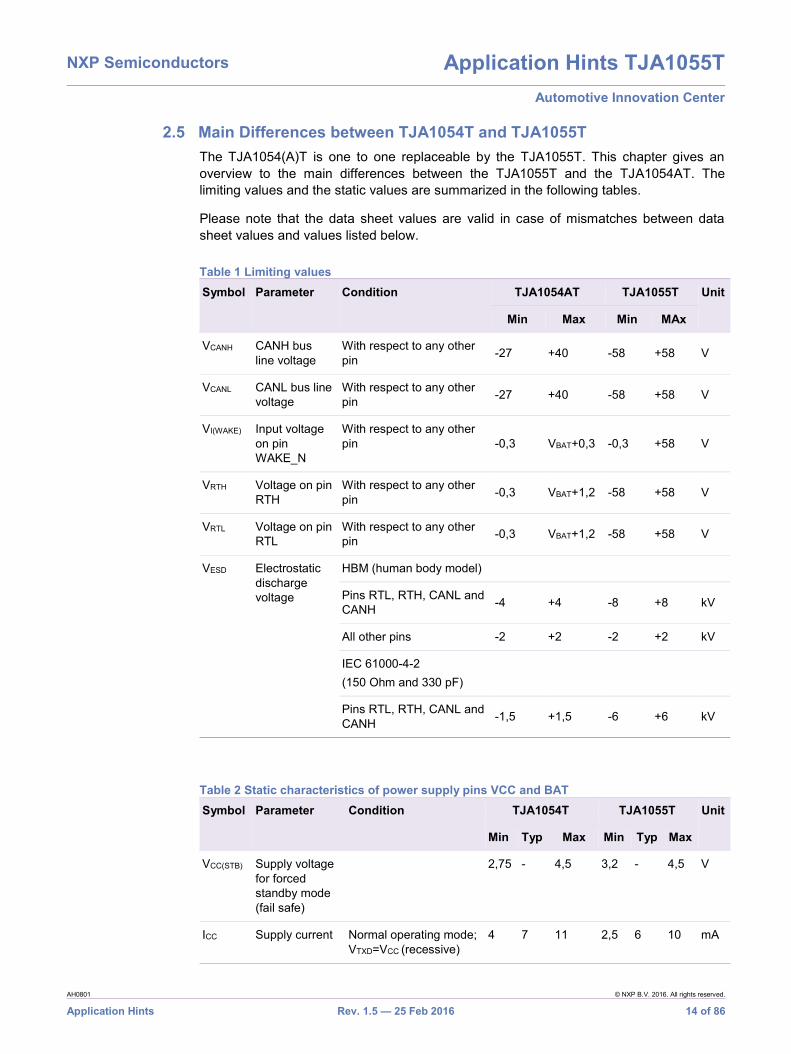
2.5 Main Differences between TJA1054T and TJA1055T The TJA1054(A)T is one to one replaceable by the TJA1055T. This chapter gives an overview to the main differences between the TJA1055T and the TJA1054AT. The limiting values and the static values are summarized in the following tables.
Please note that the data sheet values are valid in case of mismatches between data sheet values and values listed below.
Table 1 Limiting values Symbol Parameter Condition TJA1054AT TJA1055T Unit
Min Max Min MAx
VCANH CANH bus line voltage
With respect to any other pin -27 +40 -58 +58 V
VCANL CANL bus line voltage
With respect to any other pin -27 +40 -58 +58 V
VI(WAKE) Input voltage on pin WAKE_N
With respect to any other pin -0,3 VBAT+0,3 -0,3 +58 V
VRTH Voltage on pin RTH
With respect to any other pin -0,3 VBAT+1,2 -58 +58 V
VRTL Voltage on pin RTL
With respect to any other pin -0,3 VBAT+1,2 -58 +58 V
VESD Electrostatic discharge voltage
HBM (human body model)
Pins RTL, RTH, CANL and CANH -4 +4 -8 +8 kV
All other pins -2 +2 -2 +2 kV
IEC 61000-4-2 (150 Ohm and 330 pF)
Pins RTL, RTH, CANL and CANH -1,5 +1,5 -6 +6 kV
Table 2 Static characteristics of power supply pins VCC and BAT Symbol Parameter Condition TJA1054T TJA1055T Unit
Min Typ Max Min Typ Max
VCC(STB) Supply voltage for forced standby mode (fail safe)
2,75 - 4,5 3,2 - 4,5 V
ICC Supply current Normal operating mode; VTXD=VCC (recessive)
4 7 11 2,5 6 10 mA
NXP Semiconductors Application Hints TJA1055T Automotive Innovation Center
AH0801 © NXP B.V. 2016. All rights reserved.
Application Hints Rev. 1.5 — 25 Feb 2016 15 of 86
Symbol Parameter Condition TJA1054T TJA1055T Unit
Min Typ Max Min Typ Max
Normal operating mode; VTXD=0V; (dominant); no load
10 17 27 3 13 21 mA
Low power modes; VTXD=VCC
0 0 10 0 0 51 µA
VBAT Battery voltage on pin BAT
No time limit -0,3 - +40 -0,3 - +40 V
Operating mode 5,0 - 27 5,0 - 40 V
Load dump - - 40 - - 58 V
IBAT Battery current on pin BAT
All modes and in low power modes at: VRTL=VWAKE=VINH=VBAT
VBAT = 14V 10 30 50 10 25 40 µA
VBAT = 5V to 40V 5 30 125 10 25 1002 µA
Table 3 Static characteristics of input pins STB_N, EN and TXD Symbol Parameter Condition TJA1054T TJA1055T Unit
Min Typ Max Min Typ Max
VIH HIGH-level input voltage
0.7xVcc
- VCC+0.3
2.2 - 6 V
VIL LOW-level input voltage
-0.3 - 0.3xVcc
-0.3 - 0.83 V
IIH HIGH-level input current
Pins STB_N, EN VI = 4V - 9 20 - 11 21 µA
Pin TXD (54/55) VI = 4V -200 -80 -25 -160 -80 -40 µA
IIH HIGH-level input current
Pins STB_N, EN VI = 1V 4 8 - 2 11 - µA
Pin TXD (54/55) VI = 1V -800 -320 -100 -400 -240 -100 µA
1. This parameter is specified up to Tamb =-40°C to +85°C 2. This parameter is specified up to Tamb =-40°C to +125°C 3 . This parameter adapted to support 3V interfaces

NXP Semiconductors Application Hints TJA1055T Automotive Innovation Center
AH0801 © NXP B.V. 2016. All rights reserved.
Application Hints Rev. 1.5 — 25 Feb 2016 16 of 86
3. Fault-tolerant Physical Layer
3.1 The FT-CAN Principle The raising count of ECU in vehicles, especially in comfort electronics, resulted in new and advanced requirements for car bus physical layer. The CAN bus protocol provides a high robustness against communication errors, but the physical layer was the weak point (wires, connectors, etc) in a standard CAN network.
For that reason the fault-tolerant CAN (FT-CAN) was specified. It uses the redundancy two-wire communication to switch into a single wire communication in case of bus fault. This requires an enhanced termination concept. Each transceiver in a FT-CAN network must have a termination resistor for CANL and CANH. That allows developing distributed non-linear network topologies with multiple stars. For further information about the termination concept see chapter 9.1.
Additional a FT-CAN transceiver has integrated an autonomous bus failure management (BFM) in order to provide reliable failure detection with well-defined and consistent fall-back behaviour. The BFM provides fault tolerance regarding all single failures like shorts to ground or power supply or wire interruption. Switching into single wire communication in case of an error takes no longer than some milliseconds. For information about the BFM and the transceiver behaviour see chapter 9.2.
The FT-CAN transceivers TJA1054T and TJA1055T provide following features:
Differential two-wire communication Autonomous single wire communication in case of bus fault Flexible topologies
NXP Semiconductors Application Hints TJA1055T Automotive Innovation Center
AH0801 © NXP B.V. 2016. All rights reserved.
Application Hints Rev. 1.5 — 25 Feb 2016 17 of 86
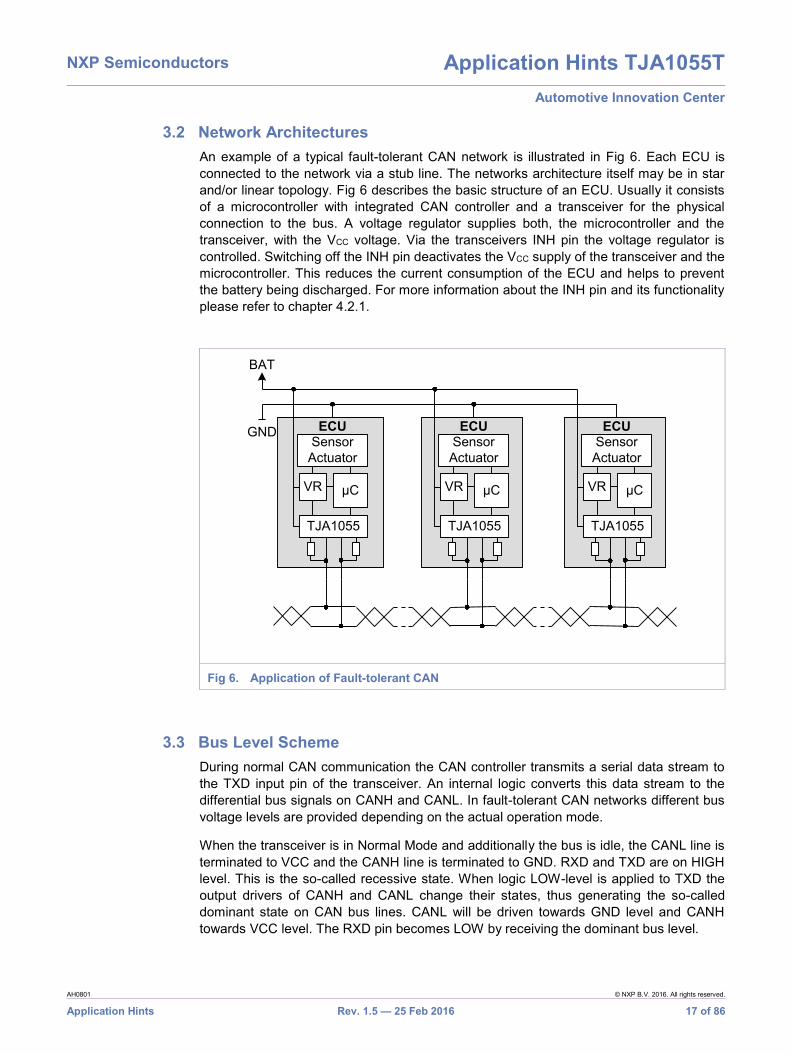
3.2 Network Architectures An example of a typical fault-tolerant CAN network is illustrated in Fig 6. Each ECU is connected to the network via a stub line. The networks architecture itself may be in star and/or linear topology. Fig 6 describes the basic structure of an ECU. Usually it consists of a microcontroller with integrated CAN controller and a transceiver for the physical connection to the bus. A voltage regulator supplies both, the microcontroller and the transceiver, with the VCC voltage. Via the transceivers INH pin the voltage regulator is controlled. Switching off the INH pin deactivates the VCC supply of the transceiver and the microcontroller. This reduces the current consumption of the ECU and helps to prevent the battery being discharged. For more information about the INH pin and its functionality please refer to chapter 4.2.1.
Fig 6. Application of Fault-tolerant CAN
3.3 Bus Level Scheme During normal CAN communication the CAN controller transmits a serial data stream to the TXD input pin of the transceiver. An internal logic converts this data stream to the differential bus signals on CANH and CANL. In fault-tolerant CAN networks different bus voltage levels are provided depending on the actual operation mode.
When the transceiver is in Normal Mode and additionally the bus is idle, the CANL line is terminated to VCC and the CANH line is terminated to GND. RXD and TXD are on HIGH level. This is the so-called recessive state. When logic LOW-level is applied to TXD the output drivers of CANH and CANL change their states, thus generating the so-called dominant state on CAN bus lines. CANL will be driven towards GND level and CANH towards VCC level. The RXD pin becomes LOW by receiving the dominant bus level.
µC
ECU
VR
TJA1055
SensorActuator
µC
ECU
VR
TJA1055
SensorActuator
µC
ECU
VR
TJA1055
SensorActuator
BAT
GND
NXP Semiconductors Application Hints TJA1055T Automotive Innovation Center
AH0801 © NXP B.V. 2016. All rights reserved.
Application Hints Rev. 1.5 — 25 Feb 2016 18 of 86
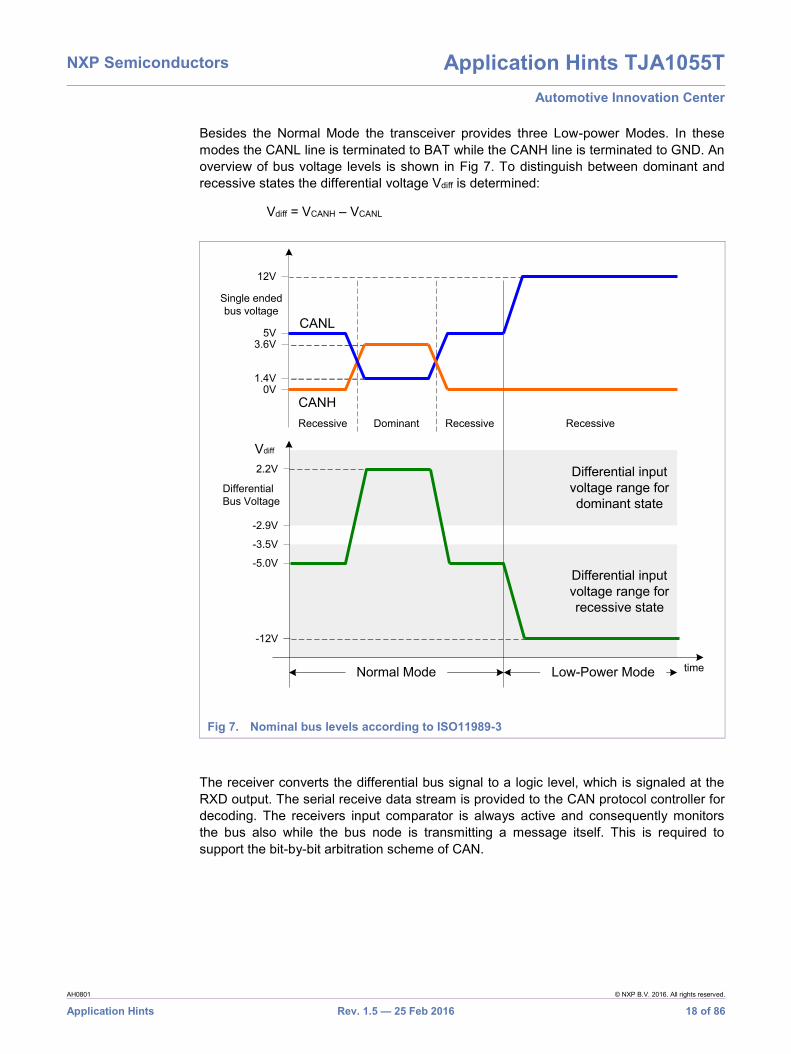
Besides the Normal Mode the transceiver provides three Low-power Modes. In these modes the CANL line is terminated to BAT while the CANH line is terminated to GND. An overview of bus voltage levels is shown in Fig 7. To distinguish between dominant and recessive states the differential voltage Vdiff is determined:
Vdiff = VCANH – VCANL
Fig 7. Nominal bus levels according to ISO11989-3
The receiver converts the differential bus signal to a logic level, which is signaled at the RXD output. The serial receive data stream is provided to the CAN protocol controller for decoding. The receivers input comparator is always active and consequently monitors the bus also while the bus node is transmitting a message itself. This is required to support the bit-by-bit arbitration scheme of CAN.
CANH
CANL
Recessive
0V1.4V
3.6V5V
RecessiveDominant Recessive
12V
Normal Mode Low-Power Mode
-2.9V
-3.5V
-12V
-5.0V
2.2V
Differential inputvoltage range forrecessive state
Differential inputvoltage range fordominant state
Single endedbus voltage
time
DifferentialBus Voltage
Vdiff

NXP Semiconductors Application Hints TJA1055T Automotive Innovation Center
AH0801 © NXP B.V. 2016. All rights reserved.
Application Hints Rev. 1.5 — 25 Feb 2016 19 of 86
4. Hardware Design
4.1 Application Diagram 3V and 5V Fig 8 shows a typical circuit diagram for the fault-tolerant CAN transceivers TJA1054(A)T and TJA1055T. For the 3V version of the TJA1055T a typical circuit is given in Fig 9 to support microcontrollers with a 3V or 3.3V interface.
The only differences between the 5V and the 3V version of the TJA1055T are the additional required pull-up resistors on RXD and ERR_N for the TJA1055T/3 to get independent from the 5V supply of the transceiver. The INH circuit, the power supply circuit, the wake pin circuit and the CAN bus circuit are equal for the 5V and the 3V version. Layout differences can only be found in the microcontroller and transceiver interface. As shown in the block diagram of the TJA1055T the pins RXD and ERR_N of the 3V version do not provide a high side driver. Thus, the transceiver is not able to pull these pins to 3V. In Fig 9 the external required pull-up resistors for RXD and ERR_N are depicted. The size of these resistors should be e.g. 3,3kOhm to get an acceptable throughput time.
The circuit diagram is split into five main sections in order to give an example layout for the TJA1054(A)T and TJA1055T. These examples are:
INH Circuit Example
Wake Pin Circuit
CAN bus circuit
µC- Transceiver Interface
BAT and VCC Supply Circuit

NXP Semiconductors Application Hints TJA1055T Automotive Innovation Center
AH0801 © NXP B.V. 2016. All rights reserved.
Application Hints Rev. 1.5 — 25 Feb 2016 20 of 86
(1) For further EMC optimization a series resistor could be applied in case the bus timing parameters allow this additional delay caused by the additional R/C time constant.
(2) Size of capacitor depends on regulator. (3) Size of termination resistors depends on system size. The overall system termination should be about 100 Ohms per CAN
line
Fig 8. Typical circuit of the TJA1054T / TJA1055T for 5V applications
(1) For further EMC optimization a series resistor could be applied in case the bus timing parameters allow this additional delay caused by the additional R/C time constant.
(2) Size of capacitor depends on regulator. (3) Size of termination resistors depends on system size. The overall system termination should be about 100 Ohms per CAN
line
Fig 9. Typical circuit of the TJA1055T/3 for 3V applications
BAT
VCCINH
BAT1k - 2k
RXD
RS> 1k8
< 180kRPull
WAKE
TXD
Note 1
ERR
EN
STB
optional
RXD
TXD
I/O
I/O
I/O
µC+
CANController
VCC
GND
150pF
RRTH
RRTL Note 3
Note 3
RTL
RTHCANHCANLGNDWake-up
CA
N B
us
optionalCommon
Mode Choke
C4
e.g.3k3
TJA
105
5/3
3VC1
Note 2
C2e.g. 10n
5V
C3e.g. 10n
optional
D1
BAT5V
INHVCC
BATe.g.10n
1k - 2k
C1Note 2
C2e.g. 10n
RXD
RS> 1k8
< 180kRPull
WAKE
TXD
Note 1
ERR
EN
STB
optional
RXD
TXD
I/O
I/O
I/O
µC+
CANController
VCC
GNDRRTH
RRTL Note 3
Note 3
RTL
RTHCANHCANLGND
Wake-upTJ
A10
54T
/ TJA
1055
T
CAN
Bus
optionalCommon
Mode Choke
e.g.100n
150pFoptional

NXP Semiconductors Application Hints TJA1055T Automotive Innovation Center
AH0801 © NXP B.V. 2016. All rights reserved.
Application Hints Rev. 1.5 — 25 Feb 2016 21 of 86
4.2 Application Details 4.2.1 INH Circuit Example
The INH pin is used to control one or more external voltage regulator(s). The transceiver INH output pin is usually directly connected to the INH input pin of the voltage regulator(s). An example schematic is illustrated in Fig 10.
Please note, that a pull-down load is required due to the possible leakage current to battery.
* Optional – See text below when using the INH pull-down resistor
Fig 10. Example: How to connect the INH pin
Maximum pull-down resistor RINH
In Sleep Mode INH is floating and in all other Modes the pin provides VBAT level. The most voltage regulators have a pull-down behavior at their INH input pins, so a floating INH pin on the transceiver switches off the voltage regulator. If there is no pull-down integrated an external pull-down resistor has to be connected. To dimension the maximum value of the pull-down resistor the leakage current of INH pin (see TJA1055T datasheet [2]) and the shutdown threshold of a voltage regulator have to be taken into account.
Table 4 Example values for resistor calculation Symbol Parameter Value Unit
|IL| Leakage current of INH pin 5 µA
V Shut down threshold of a voltage regulator 1,5 V
The maximum size of the external resistor calculates to
RINHMAX = 1,5V / 5µA = 300kOhm.
Maximum ON resistance of INH
The INH driver of the TJA1055T is designed with a self-protected high-side switch towards BAT. The maximum ON resistance calculates to
VBAT
R*INH
TJA1055TTJA1055T/3
BAT
GND
INH
INHGND
BAT
GND INH
BAT
VBAT
VBAT
3V / 5VVoltage
Regulators
VO
VO

NXP Semiconductors Application Hints TJA1055T Automotive Innovation Center
AH0801 © NXP B.V. 2016. All rights reserved.
Application Hints Rev. 1.5 — 25 Feb 2016 22 of 86
0.8V / 180uA = 4k4 (MAX) (see also datasheet, ΔVH, HIGH-level voltage drop)
So, within a certain range of output current, this worst-case pull-up resistance of 4,4kOhm is present at the INH output stage, in case it is switched on. Since the MOS transistor has a certain channel size, it can deliver a limited amount of output current within the linear operating area. Starting at about 4mA output current the linear range is left and the resistance will increase. Thus, the output will limit the short circuit current implicitly.
For applications it is recommended not to drive more than about 1mA out of the INH pin. Nevertheless the device will not be destroyed, even if the INH is shorted to GND. Due to lifetime issues it is recommended not to exceed 1mA permanently.
4.2.2 Wake_N Pin Circuit The WAKE_N pin is used for local wake-up and is both edges sensitive. It has an internal weak pull-up current source toward VBAT in order to prevent an unwanted local wake-up during an open wire at pin WAKE_N. If the WAKE_N pin is not needed it should directly connect to the BAT pin without any additional components (Fig 11b). This prevents leakage current from battery to ground.
If the local wake-up feature shall be implemented a wake-up circuit as shown in Fig 11a should be used. The WAKE_N pin is connected to VBAT via pull-up resistor. A series resistor RS is added in order to limit the current in case of lost of ground. For detailed description see below:
a With local wake-up switch
(1) The resistor value RS=1,8kOhm is necessary with a maximum battery voltage of 27V (max. battery supply for the TJA1054(A)T)
(2) The resistor value RS=2,7kOhm is necessary with a maximum battery voltage of 40V (max. battery supply for the TJA1055T)
b. No local wake-up implemented
(1) If the WAKE_N pin is not needed it should direct connect to battery to prevent unwanted local wake-up events due to noise injection
Fig 11. Example wake-up circuit; valid for both devices (TJA1055T and TJA1055T/3)
BAT
Wake
C
RBATVBAT
GND
TJA1055TTJA1055T/3
Wake-up
BAT
Wake
C
RBAT
Rs> 1k8> 2k7
Note1Note2
VBAT
Rpull
180k
GND
TJA1055TTJA1055T/3
<

NXP Semiconductors Application Hints TJA1055T Automotive Innovation Center
AH0801 © NXP B.V. 2016. All rights reserved.
Application Hints Rev. 1.5 — 25 Feb 2016 23 of 86
Remark:
Current limitation resistor RS for WAKE_N pin
As shown within the application diagram (Fig 8) of the fault-tolerant transceivers and in the figure above, a series resistor RS in front of the pin WAKE_N is recommended in case an external switch to GND should be applied. Purpose of this resistor is to limit the current, if the control unit has lost its GND connection. This resistor is needed only in case the ECU might lose its GND connection (due to a contact failure) while the external wake-up source connected to the pin WAKE_N still is connected to GND.
In case of a GND loss on ECU level there is the possibility that the entire control unit becomes connected to GND via the external wake-up switch to an independent GND source (see also Fig 12). In order to limit the current in this special failure case a series resistor is required to protect the transceiver.
Fig 12. Motivation of series resistor in WAKE_N line
The pull-up resistor RPULL shown within Fig 12 is used to guarantee a defined current within the external wake-up switch to GND in case it is closed. This current is needed to provide a good contact within the mechanical switch itself (wetting current etc.). The transceiver’s integrated pull-up current source to BAT is not suitable to provide sufficient current for the application and is used only to get a defined level at the pin WAKE in case of an open circuit condition.
Following the range of RS is shown. The value of the series resistor RS connected to the pin WAKE_N is limited by parameters summarised in Table 5. The maximum allowed current for the pin WAKE_N could be found within the “LIMITING VALUES” of the corresponding transceivers data sheet. The input threshold voltage and pull-up current for the pin WAKE_N can be found within the “DC Characteristics” section of the corresponding transceivers data sheet. The relevant values are also collected within the following table.
BAT
WAKE
GND
I <15mA
I = 1...10uA
D1
D2
BAT
GND
RS
Interruption
Filter
Transceiver
Application specificECU Load
= critical current path
ECU
(Limits critical current)
RPull

NXP Semiconductors Application Hints TJA1055T Automotive Innovation Center
AH0801 © NXP B.V. 2016. All rights reserved.
Application Hints Rev. 1.5 — 25 Feb 2016 24 of 86
Table 5 Parameters defining the range of RS Symbol Description TJA1054(A)T TJA1055T
IWAKE The maximum allowed current for the pin WAKE_N -15mA -15mA
Vth(wake) The input wake-up threshold voltage of the pin WAKE_N
2,5V 2,5V
IIL The maximum internal pull-up current of the pin WAKE_N
10uA 10uA
VGNDMAX The maximum system GND offset between ECU and the external wake-up switch, which should be tolerated (e.g.)
0,5V 0,5V
VBATMAX The maximum battery supply voltage 27V 40V
Calculating the limits of RS The maximum possible series resistor RS is defined by the wake-up threshold of the pin WAKE, the GND shift between the ECU and the transceiver and the integrated pull-up current source of the pin WAKE. Following formula allows calculation of the maximum allowed series resistor:
The minimum allowable series resistor RS is defined by the maximum allowable input current for the pin WAKE. This maximum current must not be exceeded, even if VBAT reaches its maximum voltage level. Thus the minimum series resistor RS calculates as follows
Example calculation
Assuming proper wake-up with 0,5V GND shift between the wake-up switch and the transceiver chip the maximum possible series resistor is calculated as follows (TJA1055T).
switchupwakeandrTransceivebetweenshiftGNDVwith
I
VV
I
VR
VVV
GND
IL
GNDMAXMINWAKEth
IL
RSMAXSMAX
GNDMAXMINWAKEthRSMAX
)(
)(
WAKE
BatMAXSMIN
I
VR
kOhmmA
V
I
VR
kOhmuA
VV
I
VVR
WAKE
BatMAXSMIN
IL
GNDMAXMINWAKEth
SMAX
7.215
40
20010
5.05.2)(

NXP Semiconductors Application Hints TJA1055T Automotive Innovation Center
AH0801 © NXP B.V. 2016. All rights reserved.
Application Hints Rev. 1.5 — 25 Feb 2016 25 of 86
Table 6 Maximum and minimum values of RS Conditions: GND shift VGNDMAX=0,5V; battery supply VBATMAX1054=27V and VBATMAX1055=40V
Symbol Description TJA1054(A)T TJA1055T
RSMAX Maximum series resistor 200kOhm 200kOhm
RSMIN Minimum series resistor 1,8kOhm 2,7kOhm
Note: The minimum value RS=2,7kOhm for the series resistor is only necessary in application with a maximum battery voltage of 40V. In normal passenger car applications the battery voltage is 12V and in truck applications 24V. So, there are no changes required if the TJA1054T is replaced by the TJA1055T since there is no difference in the device specification regarding this topic.
4.2.3 CAN Bus Circuit The communication in a CAN network takes place via CANH and CANL. The device pins CANH and CANL are directly connected to according bus lines. In low-power modes and in case of bus fault the CAN transmitter of the transceiver are disabled. Hence the bus pins are connected via termination resistor to RTH (CANH) and RTL (CANL) to achieve a defined output state with predefined impedance. A schematic is illustrated in Fig 13.
* Optional
Fig 13. CAN Bus Line Application Circuit
The value of the resistors RRTH and RRTL should be between 500Ohm and 6kOhm. The overall resistor in the whole CAN network should be about 100Ohm. For further information and calculation of this resistor see 9.1. To improve the EMC behavior of a FT-CAN network an optional common mode choke and capacitors could be added. The TJA1055T provides already a high ESD robustness. Further increase in ESD capability is possible with adding the PESD1CAN, if required. For further details see chapter 6.
CommonMode Choke
ESDProtection
PESD1CAN*CH*CL*
RRTL
RRTHTJA1055TTJA1055T/3
RTL
CANL
CANH
RTH

NXP Semiconductors Application Hints TJA1055T Automotive Innovation Center
AH0801 © NXP B.V. 2016. All rights reserved.
Application Hints Rev. 1.5 — 25 Feb 2016 26 of 86
4.2.4 µC- Transceiver Interface 4.2.4.1 Mode Pins EN and STB_N
The mode pins EN and STB_N control the operating modes of the TJA1055T. The transceiver provides four different modes. All modes different from normal mode are low-power modes. In these modes the current consumption is reduced significantly. The pins STB_N and EN are needed to change the transceiver operating modes as described in chapter 5.1. They are connected to a microcontroller port independently of using 3V or 5V version.
4.2.4.2 Pins TXD, RXD and ERR_N
The pins RXD and TXD are the input / output pins of the CAN controller. Data that shall be transmitted is send to the transceiver via TXD. The CAN controller listens to RXD simultaneously and evaluates the received data from the transceiver. The TXD pin can be connected directly to the dedicated 3V or 5V microcontroller interface pin.
Pin ERR_N is connected to a microcontroller port to readout an error state or one of the transceiver flags. The pins RXD and ERR_N of the 5V version provide a high-side and low-side driver, so no external pull-up resistors are needed. For the 3V version of the TJA1055T the pins RXD and ERR_N need additional external pull-up resistors (see below for the calculation of the minimum pull-up resistor). That is the only difference between these two devices. The example schematic is shown in Fig 14a and for the 5V transceiver and in Fig 14b for the 3V version.
a) Example circuit if using a 5V microcontroller * REMC is optional
b) Example circuit if using a 3V microcontroller * REMC is optional
Fig 14. RXD / TXD / ERR_N Application Circuitry
TJA1055T
R*EMC
P_x.x
P_x.x
RxD
P_x.x
TxD
R*EMC
VCC
VCC
VCC
NSTB
EN
µC + CANController
with5V interface
RxD
NERR
TxD
TJA1055T/3
R*EMC
P_x.x
P_x.x
RxD
P_x.x
TxD
R*EMC
NSTB
EN
µC + CANController
with3V interface
RxD
NERR
TxD
3V

NXP Semiconductors Application Hints TJA1055T Automotive Innovation Center
AH0801 © NXP B.V. 2016. All rights reserved.
Application Hints Rev. 1.5 — 25 Feb 2016 27 of 86
4.2.4.3 Application details for RXD and ERR_N circuitry
Both devices, the TJA1055T as well as the TJA1055T/3 are coming from the same silicon and distinguish by a bond option only. This bond option is used to activate or de-activate the high-side driver stages within the pins RXD and ERR_N.
For the TJA1055T/3 the high side driver stages connected to VCC are permanently disabled in order to prevent a reverse supply from RXD and ERR_N towards the external microcontroller port pins associated with these pins. There is no 5V (VCC) present on RXD and ERR_N at any time. As such, these pins require an external pull-up resistor towards the microcontroller supply, which in such application is usually a 3V3 supply. For details regarding dimensioning this external pull-up resistance please refer to chapter 4.2.4.4.
For the TJA1055T the high side driver stages connected to VCC are getting activated based on the BAT supply voltage. If BAT has reached an internal 3V threshold level, the high side drivers are activated and the pins RXD as well as ERR_N are providing the push-pull output behavior with VCC being the high-level output voltage. As a consequence from this internal activation circuit, the high side drivers in these pins are getting disabled again, if BAT falls below the internal 3V threshold voltage.
In case an application using the TJA1055T requires, that RXD as well as ERR_N are reliably kept HIGH even at very deep BAT voltage dips below about 3V, it is recommended to configure the associated microcontroller input pins with internal pull-up behavior. This pull-up makes sure, that RXD as well as ERR_N are kept high even during deep battery cranking conditions.
4.2.4.4 Minimum Pull-up Resistor for RXD and ERR_N for TJA1055T/3
In the TJA1055T/3 is no internal pull-up path to VCC therefore an external pull-up resistor is needed. In order to guarantee a voltage threshold for dominant and recessive states a minimum value for the pull-up resistor is required. The RXD and ERR_N pins must be able to pull-down the voltage level on the microcontroller input pin below the minimum dominant threshold. In active state there is a voltage divider consisting of the pull-up resistor Rpull-up and the internal transistor resistance RDSon (see Fig 15).
RXD
Rpull-up_min
TJA1055T/3
RDSon
µC
VCC
RXD
Vi_uC(dom)
Fig 15. Simple circuitry example of RXD and ERR_N
The transistor resistance RDSon can be calculated using the data sheet parameter IOL (LOW-level output current) [2]. On order to calculate the maximum RDSon the minimum output current must be taken into account, which is specified with 1.3mA at an output voltage of 0.4V.

NXP Semiconductors Application Hints TJA1055T Automotive Innovation Center
AH0801 © NXP B.V. 2016. All rights reserved.
Application Hints Rev. 1.5 — 25 Feb 2016 28 of 86
Based on this maximum RDSon resistance the pull-down current can be calculated, which is needed to achieve the minimum input threshold for dominant state for the microcontroller pins. For this example the minimum input voltage of the microcontroller for dominant state is assumed to be 0.3xVCC with VCC = 3V.
With this values the minimum pull-up resistor calculates to:
Rpull-up_min = (VCC – VI_uc(dom)_min) / Ipull-down = 725Ohm
Conclusion: The pull-up resistor for ERR_N and RXD should be higher than 725Ohm for a 3V application. The calculation above is an example only. It has to be re-calculated with the real values of the microcontroller interface specification and the tolerances of VCC as well as a possible microcontroller-internal pull-up resistance.
4.2.4.5 Usage of Series Resistors REMC
In Fig 14 two optional series resistor REMC in RXD and TXD wires between the µC and the transceiver may be included to further improve the EMC performance of the ECU. In case signals at TXD show fast slopes, this may cause a degradation of the system EMC performance. Here it is recommended to place a series resistor of about 1kΩ into the TXD line between transceiver and microcontroller. Along with pin capacitance this would help to smooth the edges to some degree. For high bus speeds (close to max. 125kbit/s) the additional delay within TXD has to be taken into account, especially within big networks. Also for RXD a series resistor of about 1kΩ can be used to smooth the edges at bit transitions. Again the additional delay within RXD has to be taken into account, if high bus speeds close to 125kbit/s are used within big networks.
4.2.5 BAT and VCC Supply Circuit The following considerations are recommended for the power supply of the transceiver. An example circuit is illustrated in Fig 16. The battery wire contains a blocking diode (D1) to protect the ECU components against wrong supply polarity. The capacitor C4 is needed to stabilize the battery voltage. After the capacitor the wire is split into voltage regulator and transceiver supply. The latter contains a series resistor RBAT for extra protection against automotive transients. The recommended range for the series resistor being attached to the supply pin BAT is 1 k to 2 k. The series resistance implies voltage drop on the battery supply and therefore lowers the minimum operating voltage. This voltage drop must be taken into account when determining the minimum battery operating voltage. An additional capacitor C3 of about 10nF can be used for enhanced transient protection and for stabilising the battery voltage. It is recommended that this capacitor is connected to the BAT pin as close as possible.
3083.1
4.0
mA
V
I
VR
OL
O
RDSon
mAR
VCC
R
VI
RDSonRDSon
domuCI
downpull 9.23.0min_)(_

NXP Semiconductors Application Hints TJA1055T Automotive Innovation Center
AH0801 © NXP B.V. 2016. All rights reserved.
Application Hints Rev. 1.5 — 25 Feb 2016 29 of 86
Fig 16. Example of power supply circuit for the 5V device
Fig 17. Example of power supply circuit for the 3V device with two voltage regulators
The voltage regulator delivers the operation current to the VCC pin of the transceiver. The VCC supply of the TJA1055T must be able to deliver current of 100mA in average for the transceiver output transmitter (ICC_NORM_AVG, see chapter 4.2.6). Using a linear voltage regulator and to actuate the device in all conditions, it is recommended to stabilize the output voltage with a bypass capacitor C1 of about 20F. Its purpose is to buffer disturbances on the battery line and to buffer extra supply current demand in case of bus failures. It is usually placed at the output of the voltage regulator. Typically, a second capacitor C2 is integrated close to the transceiver. The size of this capacitor should be between 10-47nF and should also be placed as close as possible to the VCC pin of the transceiver. For reliability reasons it might be useful to apply two capacitors in series connection between VCC and GND. Thus, a single shorted capacitor (e.g. damaged device) cannot short-circuit the VCC supply.
INH
VCC
C1e.g. 20µ
BAT
C2e.g. 10n
C3e.g. 10n
RBAT1k - 2k
µC
TJA1055TJA1055/3
Voltageregulator
BAT
D1 C4
optionalRINH
INHVCC
C1e.g. 20µ
BAT
C2e.g. 10n
C3e.g. 10n
RBAT1k - 2k
C4 µC
TJA1055TJA1055/3
3V Voltageregulator
5V Voltageregulator
BAT
D1
optionalRINH

NXP Semiconductors Application Hints TJA1055T Automotive Innovation Center
AH0801 © NXP B.V. 2016. All rights reserved.
Application Hints Rev. 1.5 — 25 Feb 2016 30 of 86
4.2.6 Current Consumption on BAT Pin Battery Supply Current
The battery current consumption of the TJA1055T in low power mode is typical 25µA with an applied battery voltage of 14V. If there is a low battery voltage of 7V-8V the undervoltage detector of the transceiver becomes active requiring extra current to generate more accurate voltage thresholds. This improves the undervoltage detection of the TJA1055T compared to the TJA1054T. For the TJA1055T the power-on flag is set earliest at 5V and latest at 4V battery voltage. For the TJA1054T this is guaranteed between 3,5V down to 1V.
Voltage drop on Series Resistor at BAT Pin
The following considerations are recommended for the determination of the series resistor (RBAT) being attached to the supply input BAT of the TJA1054T / TJA1055T transceiver products. The minimum recommended series resistance is about 1k for protection against automotive transients. On the other hand the series resistance implies voltage drop on the battery supply and therefore lowers the minimum operating voltage. The voltage drop across the RBAT series resistance can be calculated with the following consideration:
VDROPLPM = RBAT * (IBATmaxL + IIL + IINH + IRTL)
VDROPLPM Maximum voltage drop in low power mode RT Series resistor at BAT pin IBATmaxL Maximum battery supply current in low power modes (VBAT = 5V to 40V) IIL WAKE input current, if VWAKE_N = 0 IINH Maximum INH load, when used IRTL Maximum RTL current in low power modes (VRTL = 0)
Table 7 Example calculation of worst-case voltage drop on battery series resistor Example values according TJA1055T datasheet Rev.03 – 13 March 2007 [2] Example values according TJA1054T datasheet 11th February 2002 [3]
Symbol Description Condition TJA1054T TJA1055T
VBAT Operating voltage 5V – 27V 5V – 40V
IBAT Maximum battery supply current
TJA1054T: VBAT = 12V TJA1055T: VBAT = 14V
50µA 40 µA
IBATmaxL Maximum battery supply current (low-power-modes)
TJA1054T: VBAT=5V to 27V TJA1055T: VBAT=5V to 40V
125µA 100µA
NXP Semiconductors Application Hints TJA1055T Automotive Innovation Center
AH0801 © NXP B.V. 2016. All rights reserved.
Application Hints Rev. 1.5 — 25 Feb 2016 31 of 86
Symbol Description Condition TJA1054T TJA1055T
IIL WAKE input current VWAKE_N = 0V TJA1054T: VBAT=5V to 27V TJA1055T: VBAT=5V to 40V
10µA 12µA
IINH Maximum recommended INH load (when used)
1mA 1mA
IRTL Maximum RTL current in low power modes
Dominant: VRTL = 0 1.25mA 1.50mA
RT Series resistor at BAT pin 1k 1k
IBATTLPM Maximum total battery current in low power mode
Standby Mode T < 1.6 ms Dominant bus VWAKE_N = 0V
2.38mA 2.61mA
VDROPLPM1 Maximum voltage drop in low power mode
Standby Mode T < 1.6 ms Dominant bus VWAKE_N = 0V RT = 1kOhm
2.38V 2.61V
VDROPLPM2 Maximum voltage drop in low power mode without INH load
Standby Mode T < 1.6 ms Dominant bus INH not used RT = 1kOhm
1.38V 1.61V
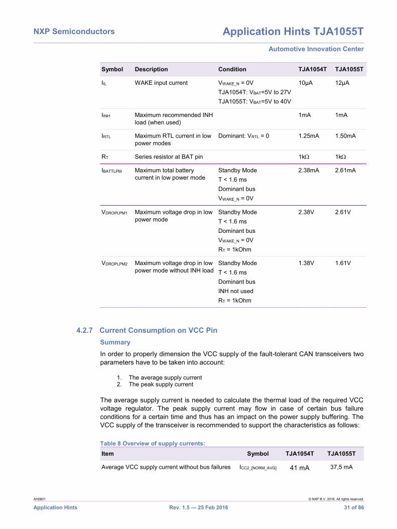
4.2.7 Current Consumption on VCC Pin Summary
In order to properly dimension the VCC supply of the fault-tolerant CAN transceivers two parameters have to be taken into account:
1. The average supply current 2. The peak supply current
The average supply current is needed to calculate the thermal load of the required VCC voltage regulator. The peak supply current may flow in case of certain bus failure conditions for a certain time and thus has an impact on the power supply buffering. The VCC supply of the transceiver is recommended to support the characteristics as follows:
Table 8 Overview of supply currents: Item Symbol TJA1054T TJA1055T
Average VCC supply current without bus failures ICC2_[NORM_AVG] 41 mA 37,5 mA

NXP Semiconductors Application Hints TJA1055T Automotive Innovation Center
AH0801 © NXP B.V. 2016. All rights reserved.
Application Hints Rev. 1.5 — 25 Feb 2016 32 of 86
Item Symbol TJA1054T TJA1055T
Average VCC supply current at presence of single bus failures ICC3_[SC1_AVG] 76 mA 72,5 mA
Worst case peak VCC supply current at presence of single bus failure (for 6 bit times max.) ICC3_[SC1_DOM] 141 mA 135 mA
Worst case peak VCC supply current at presence of dual bus failures (for 17 bit times max.) ICC4_[SC2_DOM] 142 mA 136 mA
The capacitive buffering needed for the transceiver depends on the systems power concept and the regulator characteristic of the used voltage regulator chip.
In case the transceiver has a separated VCC power supply apart from the microcontroller, the peak supply current during single bus failures is relevant because here the communication medium has to keep unaffected. The worst-case dual failure situation is not relevant since here the communication medium is completely out of operation and the transceiver does not need to be supplied anymore. Such systems are recommended to provide a bypass capacitance of 47 µF in order to support single wiring faults. Depending on the regulator behavior this capacitance may become smaller if the regulation time constant is fast enough.
In case the transceiver’s VCC power supply is shared with its host microcontroller, the peak supply current during the worst-case dual failure situation has to be taken into account. This is because the µC has to keep a proper supply even if there is no CAN communication possible at all. Such systems are recommended to provide a bypass capacitance of 100uF. Depending on the regulator behavior this capacitance may become much smaller if the regulation time constant is fast enough.
This capacitance can be implemented as a separate component or alternatively through a corresponding increase of the capacitance of the bypass capacitor being located at the VCC voltage regulator.
In the following, relevant cases are considered in more detail.

NXP Semiconductors Application Hints TJA1055T Automotive Innovation Center
AH0801 © NXP B.V. 2016. All rights reserved.
Application Hints Rev. 1.5 — 25 Feb 2016 33 of 86
4.2.7.1 Average Supply Current; no Bus Short-Circuit Conditions
In recessive state the different transceivers are consuming a VCC supply current as listed in the corresponding data sheets. In dominant state the VCC supply current is calculated by the addition of the IC-internal supply current (see data sheet TJA1055T: “no load” condition) and the output current at pins CANH and RTL. The reason for taking the currents of CANH and RTL is, because CANH has an internal path to GND and is pulled to VCC in case of a dominant bit. So, the current flows from the transceiver into the network. CANL has an internal path to VCC and is pulled to GND in case of a dominant bit. Therefore the current flows from the network through the transceiver to GND. CANL still has a connection to VCC via RTL and the maximum current that can flow out of RTL through the resistor into the transceiver again is limited by the value of the resistor which is 1kOhm is the example below.
Maximum dominant supply current without bus wiring faults The maximum dominant supply current (without bus wiring faults) can calculate by following equations.
ICC1_[DOM_MAX] = ICC_[DOM] + ICANH_[DOM] + IRTL_[DOM]
IRTL_[DOM] = (VCC - VCANL_DOM) / RT
Table 9 Maximum dominant supply current without bus wiring faults: Item Symbol TJA1054T TJA1055T
VCC supply current dominant, max, no load ICC_[DOM] 27 mA 21 mA
CANH dominant current ICANH_[DOM] 40 mA 40 mA
Assumed termination resistor RT 1 k 1k
Assumed CANL dominant voltage VCANL_DOM 1 V 1V
TJA1054T : ICC1_[DOM_MAX] 1054 = 27mA + 40 mA + (5V - 1V) / 1k = 71 mA max.
TJA1055T : ICC1_[DOM_MAX] 1055 = 21mA + 40 mA + (5V - 1V) / 1k = 65 mA max.
Thermal considerations without bus wiring faults
For thermal considerations the average supply current at pin VCC is relevant considering the transmit duty cycle. In the following example a continuously transmitting node is assumed. This might happen e.g. if a node starts a transmission while the rest of the network does not respond with an acknowledge for some reason. Typically a much lower duty cycle is relevant since a node transmits messages within certain time slots only, depending on the applications network management. With an assumed transmit duty cycle of 50% on pin TXD, the maximum average supply current is
ICC2_[NORM_AVG] = 0.5 * (ICC_[REC] + ICC1_[DOM_MAX])
Table 10 Thermal considerations without bus wiring faults: Item Symbol TJA1054T TJA1055T
VCC supply current recessive, max. ICC_[REC] 11 mA 10 mA
TJA1054T : ICC2_[NORM_AVG] 1054 = 0.5 * (11mA + 71mA) = 41 mA max.
TJA1055T : ICC2_[NORM_AVG] 1055 = 0.5 * (10mA + 65mA) = 37,5 mA max.

NXP Semiconductors Application Hints TJA1055T Automotive Innovation Center
AH0801 © NXP B.V. 2016. All rights reserved.
Application Hints Rev. 1.5 — 25 Feb 2016 34 of 86
Average supply current; with a short-circuit of one bus wire
The maximum VCC supply current occurs with a bus wire short-circuit between CANH and GND. In this case the CANH outputs a maximum short circuit current in dominant state (see data sheets). For thermal considerations the average supply current is relevant. For buffering considerations the maximum dominant supply current is relevant.
Maximum dominant supply current with CANH shorted to GND
ICC3_[SC1_DOM] = ICC_[DOM] + IO(CANH)_[DOM] + IRTL_[DOM] (t < 6 bit times)
The 6-bit time limitation is caused by a supposed Error Flag to be sent by the CAN Controller.
Table 11 Maximum dominant supply current with CANH shorted to GND: Item Symbol TJA1054T TJA1055T
CANH dominant output current, short circuit IO(CANH)_[DOM] 110 mA 110 mA
TJA1054T : ICC3_[SC1_DOM] 1054 = 27mA + 110 mA + (5V - 1V) / 1k = 141 mA max.
TJA1055T : ICC3_[SC1_DOM] 1055 = 21mA + 110 mA + (5V - 1V) / 1k = 135 mA max.
Thermal considerations with CANH shorted to GND
For thermal considerations the average supply current at pin VCC is relevant considering the transmit duty cycle. With a transmit duty cycle of 50% on pin TXD, the maximum average supply current at CANH to GND short-circuit is:
ICC3_[SC1_AVG] = 0.5 * (ICC_[REC] + ICC3_[SC1_DOM])
Thermal considerations with CANH shorted to GND:
TJA1054T : ICC3_[SC1_AVG] 1054 = 0.5 * (11mA + 141mA) = 76 mA max.
TJA1055T : ICC3_[SC1_AVG] 1055 = 0.5 * (10mA + 135mA) = 72,5 mA max.
VCC extra supply current in single fault condition
Compared to the quiescent current in recessive state the maximum extra supply current when the CANH driver is turned on with CANH shorted to GND is needed to calculate the required worst case VCC buffer capacitance. This extra supply current has to be buffered for up to 6 bit times, depending on the applications voltage regulator.
ICC3_SC1 = ICC3_[SC1_DOM] – ICC_[REC_MIN]
Table 12 VCC extra supply current in case of single fault condition: Item Symbol TJA1054T TJA1055T
Min VCC supply current, recessive ICC_[REC_MIN] 4 mA 2,5 mA
TJA1054T : ICC3_SC1 1054 = 141 mA - 4 mA = 137 mA max.
TJA1055T : ICC3_SC1 1055 = 135 mA – 2,5 mA = 132,5 mA max.
NXP Semiconductors Application Hints TJA1055T Automotive Innovation Center
AH0801 © NXP B.V. 2016. All rights reserved.
Application Hints Rev. 1.5 — 25 Feb 2016 35 of 86
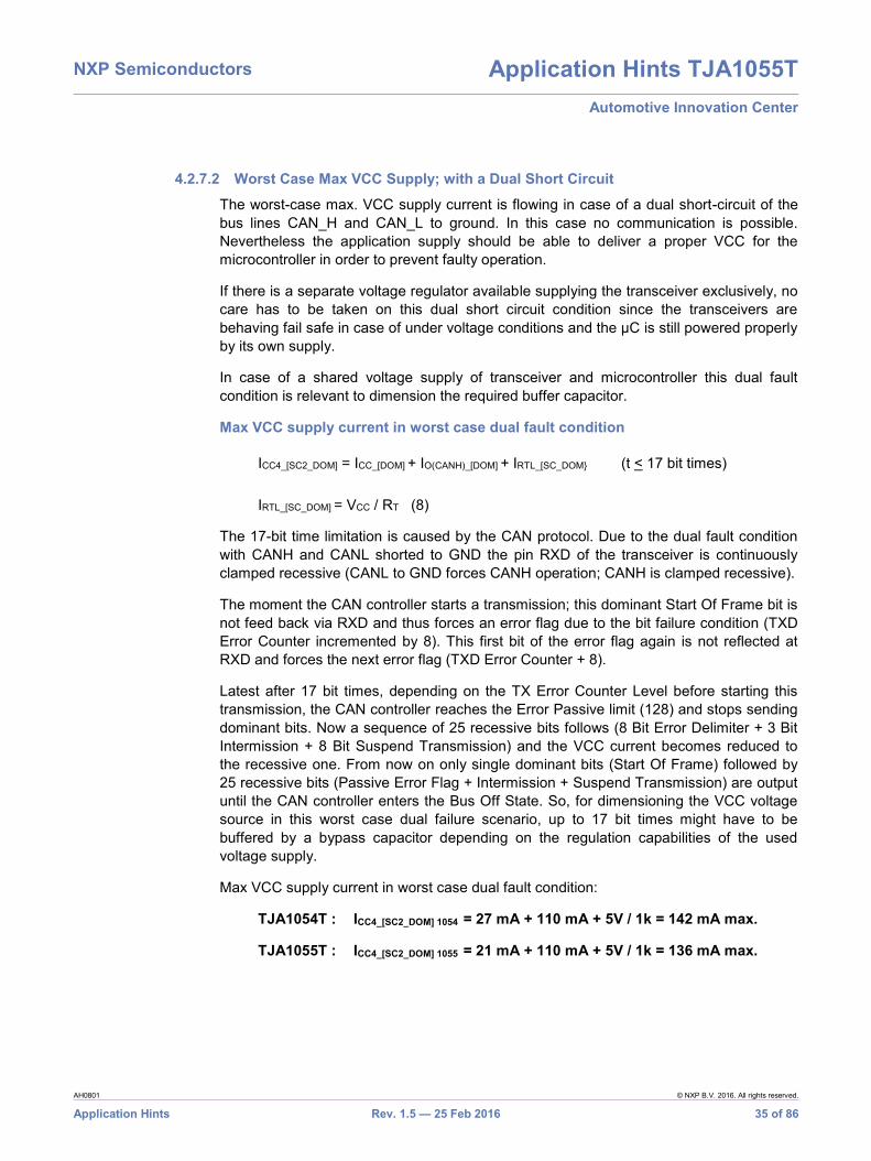
4.2.7.2 Worst Case Max VCC Supply; with a Dual Short Circuit
The worst-case max. VCC supply current is flowing in case of a dual short-circuit of the bus lines CAN_H and CAN_L to ground. In this case no communication is possible. Nevertheless the application supply should be able to deliver a proper VCC for the microcontroller in order to prevent faulty operation.
If there is a separate voltage regulator available supplying the transceiver exclusively, no care has to be taken on this dual short circuit condition since the transceivers are behaving fail safe in case of under voltage conditions and the µC is still powered properly by its own supply.
In case of a shared voltage supply of transceiver and microcontroller this dual fault condition is relevant to dimension the required buffer capacitor.
Max VCC supply current in worst case dual fault condition
ICC4_[SC2_DOM] = ICC_[DOM] + IO(CANH)_[DOM] + IRTL_[SC_DOM (t < 17 bit times)
IRTL_[SC_DOM] = VCC / RT (8)
The 17-bit time limitation is caused by the CAN protocol. Due to the dual fault condition with CANH and CANL shorted to GND the pin RXD of the transceiver is continuously clamped recessive (CANL to GND forces CANH operation; CANH is clamped recessive).
The moment the CAN controller starts a transmission; this dominant Start Of Frame bit is not feed back via RXD and thus forces an error flag due to the bit failure condition (TXD Error Counter incremented by 8). This first bit of the error flag again is not reflected at RXD and forces the next error flag (TXD Error Counter + 8).
Latest after 17 bit times, depending on the TX Error Counter Level before starting this transmission, the CAN controller reaches the Error Passive limit (128) and stops sending dominant bits. Now a sequence of 25 recessive bits follows (8 Bit Error Delimiter + 3 Bit Intermission + 8 Bit Suspend Transmission) and the VCC current becomes reduced to the recessive one. From now on only single dominant bits (Start Of Frame) followed by 25 recessive bits (Passive Error Flag + Intermission + Suspend Transmission) are output until the CAN controller enters the Bus Off State. So, for dimensioning the VCC voltage source in this worst case dual failure scenario, up to 17 bit times might have to be buffered by a bypass capacitor depending on the regulation capabilities of the used voltage supply.
Max VCC supply current in worst case dual fault condition:
TJA1054T : ICC4_[SC2_DOM] 1054 = 27 mA + 110 mA + 5V / 1k = 142 mA max.
TJA1055T : ICC4_[SC2_DOM] 1055 = 21 mA + 110 mA + 5V / 1k = 136 mA max.
NXP Semiconductors Application Hints TJA1055T Automotive Innovation Center
AH0801 © NXP B.V. 2016. All rights reserved.
Application Hints Rev. 1.5 — 25 Feb 2016 36 of 86
4.2.7.3 VCC extra supply current in dual fault condition
Compared to the quiescent current in recessive state the maximum extra supply current when the CANH driver is turned on in dual short-circuit condition is needed to calculate the required worst case VCC buffer capacitance. This extra supply current has to be buffered for that time the applications voltage regulator needs to react.
ICC4_SC2 = ICC4_[SC2_DOM] – ICC_[REC]
VCC extra supply current in case of dual fault condition:
Table 13 VCC extra supply current in case of single fault condition Item Symbol TJA1054T TJA1055T
Min VCC supply current, recessive ICC_[REC] 4 mA 2,5 mA
TJA1054T : ICC4_SC2 1054 = 142 mA - 4 mA = 138 mA max.
TJA1055T : ICC4_SC2 1055 = 136 mA – 2,5 mA = 133,5 mA max.
4.2.7.4 Calculation of worst-case bypass capacitor
Depending on the power supply concept, the required worst-case bypass capacitor can be calculated. In case of a separate VCC supply for the transceiver only, the extra supply current ICC3_SC1 in case of the single fault condition has to be taken with a maximum of 6 dominant bit times (length of error frame).
If the transceiver and the host microcontroller are supplied from the same regulator (shared VCC supply), the extra supply current ICC4_SC2 in case of the dual fault condition has to be taken with a maximum of 17 dominant bit times.
CBUFF = ICCx_SCx * tDOM_MAX / VMAX (10)
The capacitor CBUFF is needed if the voltage regulator is not able to deliver any extra current within the maximum dominate output drive tDOM_MAX during the dual fault condition.
Example calculation, separate supplied transceiver @ 83,33kBit/s
In case of a separate transceiver supply the bypass capacitance has to be calculated based on the single fault condition with CANH shorted to GND. Here the dual fault is not relevant.
Assumption of 83,33 kBit/s: tDOM_MAX = 6 * 12 us = 72 us
Maximum allowed VCC voltage drop: VMAX = 0.25V
TJA1054T : CBUFF 1054 = 137 mA * 72 us / 0.25 V = 39,5 µF
TJA1055T : CBUFF 1055 = 132,5 mA * 72 us / 0.25 V = 38,2 µF
In this example the bypass capacitance to be reserved for the VCC supply of the TJA1055T transceiver is recommended to be 39,9 µF minimum at 83,33 kBit/s. It may

NXP Semiconductors Application Hints TJA1055T Automotive Innovation Center
AH0801 © NXP B.V. 2016. All rights reserved.
Application Hints Rev. 1.5 — 25 Feb 2016 37 of 86
become smaller, if the used voltage regulator is able to deliver an extra current within tDOM_MAX.
Example calculation, shared supply
In case of a shared supply concept the bypass capacitance has to be calculated based on the worst-case dual fault condition in order to keep the µC supply stabile:
Assumption of 83,33 kBit/s: tDOM_MAX = 17 * 12 us = 204 us
Maximum allowed VCC voltage drop: VMAX = 0.25V
TJA1054T : CBUFF 1054 = 138 mA * 204 us / 0.25 V = 113 µF
TJA1055T : CBUFF 1055 = 133,5 mA * 204 us / 0.25 V = 109 µF
In this example the bypass capacitance to be reserved for the VCC supply of the transceiver is recommended to be 114 µF minimum at 83,33 kBit/s. It may become smaller, if the used voltage regulator is able to deliver an extra current within tDOM_MAX.
4.3 Application Example: Wake-up via RXD / ERR_N without VCC There are application cases where the microcontroller stays powered all time while the transceiver becomes unpowered on VCC side in order to safe some power dissipation. In order to wake-up the microcontroller through the transceiver it is required to signal a wake-up towards the microcontroller through the typical interface RXD and ERR_ N. For applications based on the TJA1054T it was not possible to wake-up the system through RXD and ERR_ N while VCC was off.
Fig 18. Example of application circuit with different supply of µC and Transceiver
In the application case shown in Fig 18 the TJA1055T provides a new feature compared to the TJA1054T. The TJA1055T is able to signal a wake-up on RXD and ERR_N even if the VCC of the transceiver is switched off.
BAT
VCCINH
BAT
RXD
WAKE
TXD
ERR
EN
STB
RXD
TXD
I/O
I/O
I/O
µC+
CANController
VCC
GNDRRTH
RRTL
RTL
RTHCANHCANLGNDWake-up
CAN Bus
e.g.3k3
TJA
1055
TTJ
A10
55T/
3
5V or3V5V
Permanently VCC supplied

NXP Semiconductors Application Hints TJA1055T Automotive Innovation Center
AH0801 © NXP B.V. 2016. All rights reserved.
Application Hints Rev. 1.5 — 25 Feb 2016 38 of 86
4.3.1 Application Description In the above example, the microcontroller is supplied permanently out of a 3V or 5V voltage regulator. RXD and ERR_N have a pull-up resistor to the µC voltage supply. The 5V supply of the transceiver is switched off in low-power mode. For the TJA1055T the pins RXD and ERR_N are not following the VCC supply voltage towards low level with VCC off. This feature makes it possible to wake-up the supplied microcontroller through an unsupplied (VCC off, but BAT on) transceiver via RXD and ERR_N. For additional information see next chapter.
In case a TJA1054T becomes un-powered, the pins RXD and ERR_N are actively going to low level due to the pin-internal diode structures. Consequently a TJA1054T cannot signal a wake-up on RXD and ERR_N with VCC off, because the pins are already low while VCC is off.
For applications, which do not use this feature, there is no difference. It just offers some more freedom in the ECU design. So, there is no issue with drop-in replacement of the TJA1054T.
4.3.2 Wake-up capability of the TJA1055T with VCC off The RXD and ERR_N pins of the TJA1055T have a reverse current protection diode in their VCC path (see Fig 19). This allows connecting these pins with pull-up resistors to the supply voltage of the microcontroller in order to prevent the floating behaviour of the pins when the transceiver becomes un-powered. In Normal Mode the diode is bypassed to remove the voltage drop.
Fig 19. Differences of the internal circuit of the TJA1055T and TJA1054T
For the 3V version of the TJA1055T the VCC path is not integrated. So the TJA1055T/3 provides also the wake-up capability with VCC off.
RXD
VCC
GND
LPM*
RXD
GND
RXD
VCC
GND
TJA1055T TJA1055T/3 TJA1054T

NXP Semiconductors Application Hints TJA1055T Automotive Innovation Center
AH0801 © NXP B.V. 2016. All rights reserved.
Application Hints Rev. 1.5 — 25 Feb 2016 39 of 86
5. Software Design
5.1 Operation Mode Control 5.1.1 Overview
The transceiver is controlled via mode pins EN and STB_N. These pins are transceiver input pins and are connected to the host microcontroller. Only the microcontroller is able to change the operating modes of the transceiver. The transceiver is powered directly from the battery supply via the pin BAT. This allows disabling the VCC supply entirely during time phases, the CAN bus is not required by the system.
The TJA1055T provides one normal operating mode and four low-power modes. The Table 14 gives an overview of the operating modes of the FT-CAN transceiver.
Table 14 Overview of operation modes Modes EN STB_N Description
Normal Mode 1 1 Normal transceiver operation
Go-to-Sleep 1 0 Switches off the INH pin after a certain time out to disable the external voltage regulator
Standby / Sleep 0 0 In Standby the INH pin is on In Sleep the INH pin is off
Power-on Standby 0 1 Allows to read back the Power-on flag
In case of VCC undervoltage condition the transceiver switches automatically into forced standby mode (except during Sleep Mode). The transceiver keeps this forced standby mode until the VCC undervoltage condition is left.
For wake-up purposes a battery-related WAKE_N pin is provided. In addition to bus failure information and the CAN received bit stream, the pins ERR_N and RXD are used to signal wake-up requests towards the application controller.

NXP Semiconductors Application Hints TJA1055T Automotive Innovation Center
AH0801 © NXP B.V. 2016. All rights reserved.
Application Hints Rev. 1.5 — 25 Feb 2016 40 of 86
5.1.2 Normal Mode (‘1’ ‘1’) The Normal Mode is entered setting STB_N=1 and EN=1 (‘1’ ‘1’). During Normal Mode the INH pin is active high and the transceiver is used to transmit data to the bus and to receive data from the CAN bus. The digital input bit stream at TXD is transferred into the corresponding analog bus signal at CANH and CANL. Simultaneously, the analog bus signal is monitored and converted into the corresponding digital bit stream at RXD. In this mode the pin ERR_N is used to readout bus failure conditions with an active LOW behaviour.
Table 15 Description of applied pin value in Normal Mode VBAT=12V, VCC=5V and GND=0V
PIN STATE Description of applied pin value
INH HIGH An external connected voltage regulator is enabled
EN HIGH Transceiver is in Normal only if EN and STB_N are HIGH
STB_N HIGH
TXD HIGH Recessive transmit data
LOW Dominant transmit data
RXD HIGH Recessive received data
LOW Dominant received data
ERR_N HIGH No error occur
LOW Error flag is signaled
CANL VCC Recessive bus signal
1,4V to GND Dominant bus signal
CANH GND Recessive bus signal
VCC to 3,6 V Dominant bus signal
5.1.3 Low-power Mode: Go-to-Sleep (‘0’ ‘1’) The low-power mode Go-to-Sleep is a command to set the transceiver into Sleep Mode. Entering Go-to-Sleep the transceiver immediately changes into low-power operation, while the pin INH still keeps active HIGH for a certain time. Entering Go-to-Sleep an internal wake-up flip-flop is output via the pins RXD and ERR_N, if VCC is present. Thus both signals can be used to wake-up the application with an active low signal. If the Go-to-Sleep state keeps present for a certain time (5...50µs; see data sheet TJA1055T: “ td(sleep) delay time to sleep) the INH output of the TJA1055T becomes “floating” disabling the externally connected voltage regulator. Once the 50us Go-to-Sleep command time is passed, it is recommended to set EN actively to LOW level under software control. The Sleep Mode shall be activated before VCC has fallen below 4V in order to enter Sleep Mode successfully (see also Fig 20 and Fig 29). In case the Sleep Mode transition is not performed actively with VCC > 4V, there might be a slightly increased sleep current consumption (45A instead of 25A).

NXP Semiconductors Application Hints TJA1055T Automotive Innovation Center
AH0801 © NXP B.V. 2016. All rights reserved.
Application Hints Rev. 1.5 — 25 Feb 2016 41 of 86
Table 16 Description of applied pin value in Low-power Mode: Go-To-Sleep VBAT=12V, VCC=5V and GND=0V
PIN STATE Description of applied pin value
INH HIGH t < Treact(Sleep)
Float t > Treact(Sleep)
EN HIGH Transceiver is in Go-To-Sleep Mode only if EN = HIGH and STB_N = LOW STB_N LOW
TXD X Don’t care
RXD HIGH No wake-up signal is detected
LOW Wake-up signal is detected
ERR_N HIGH No wake-up signal is detected
LOW Wake-up signal is detected
CANL VBAT Bus idle value
CANH GND Bus idle value
Timings for a valid Go-To-Sleep Command
The Go-to-Sleep filter timer of the transceiver is specified in a range of 5µs up to 50µs (see datasheet TJA1055T: td(sleep) delay time to sleep). That means that a Go-to Sleep command shorter than 5µs is ignored and a command longer than 50µs by guarantee will disable the INH pin and the transceiver will enter Sleep Mode. To guarantee a successful mode transition under all conditions, the maximum specified time for Go-to-Sleep command must be applied on the mode pins.
Fig 20. Timings for valid Go-To-Sleep Command and reactions of INH pin
could be validignored guaranteed
NSTB
EN
INH
0 5µs 20µs 50µs

NXP Semiconductors Application Hints TJA1055T Automotive Innovation Center
AH0801 © NXP B.V. 2016. All rights reserved.
Application Hints Rev. 1.5 — 25 Feb 2016 42 of 86
5.1.4 Low-power Mode: Standby / Sleep (‘0’ ‘0’) The Standby or Sleep Mode is entered setting STB_N=0 and EN=0. The internal “sub-modes” Standby and Sleep are distinguished only by the state of the pin INH. In Standby Mode the INH pin remains active and the external voltage regulator stays alive, this mode can be entered directly from Normal Mode. The Sleep Mode is entered with a previous successful Go-to-Sleep procedure. During Sleep Mode the pin INH is floating and switches off an external voltage regulator. During Standby or Sleep Mode the pins RXD and ERR_N are signaling a possible wake-up condition (see Table 17 and chapter 5.2). A wake-up is caused by an edge event at WAKE_N pin or via CAN bus traffic.
ATTENTION: A mode transition to any other mode via mode control pins EN and STB_N is only possible if supply voltage VCC is present. In Sleep Mode the INH pin and the external voltage regulator is switched off, so VCC is also off. A received wake-up event activates the pin INH again and thus VCC.
Table 17 Description of applied pin value in Low-power Mode: Standby / Sleep VBAT=12V, VCC=5V / 0V and GND=0V
PIN STATE Description of applied pin value
INH
HIGH Standby:
An external connected voltage regulator is enabled
Float Sleep:
A external connected voltage regulator is disabled
EN LOW Transceiver is in Standby or Sleep Mode only if EN and STB_N are both LOW STB_N LOW
TXD X Don’t care
RXD1 HIGH No wake-up signal is detected
LOW Wake-up signal is detected
ERR_N4 HIGH No wake-up signal is detected
LOW Wake-up signal is detected
CANL VBAT Bus idle value
CANH GND Bus idle value
4. The TJA1055 allows keeping RXD and ERR_N on high level, even if VCC is switched off. This can be achieved with an external pull-up to the VCC supply of the microcontroller (e.g. via the internal pull-up of the corresponding I/O port). Thus, even without VCC present, a wake-up can be signaled with an active LOW signal. This is in contrast to the TJA1054T(A) which always pulls these pins to LOW level with VCC off due to internal diodes to VCC.

NXP Semiconductors Application Hints TJA1055T Automotive Innovation Center
AH0801 © NXP B.V. 2016. All rights reserved.
Application Hints Rev. 1.5 — 25 Feb 2016 43 of 86
5.1.5 Low-power Mode: Power-on Standby (‘1’ ‘0’) The Power-on Standby Mode is entered setting STB_N=1 and EN=0. This mode behaves similar to Standby Mode (see above) with the difference that the pin ERR allows reading back the internal PWON flag. This flag is set whenever the transceiver is powered with battery supply the first time or after BAT undervoltage detection. So the application can distinguish between a cold start situation caused by a system sleep or a cold start due to first battery connection of the device. The meaning of the pins in that mode is summarized in Table 18.
Table 18 Description of applied pin value in Low-power Mode: Power-on Standby VBAT=12V, VCC=5V and GND=0V
PIN STATE Description of applied pin value
INH HIGH An external connected voltage regulator is enabled
EN LOW Transceiver is in Power-on Standby Mode only if EN = LOW and STB_N = HIGH STB_N HIGH
TXD X Don’t care
RXD HIGH No wake-up signal is detected
LOW Wake-up signal is detected
ERR_N HIGH No power-on event
LOW Power-on event detected
CANL VBAT Bus idle value
CANH GND Bus idle value
The power-on flag is set with VBAT falling below Vpof(BAT) (see [2]: power-on flag voltage on pin BAT). This flag has the highest priority and locks the transceiver from entering sleep mode. To delete the power-on flag the transceiver has to enter the normal mode once for at least 500ns (see also Fig 21).

NXP Semiconductors Application Hints TJA1055T Automotive Innovation Center
AH0801 © NXP B.V. 2016. All rights reserved.
Application Hints Rev. 1.5 — 25 Feb 2016 44 of 86
(1) Pending power-on flag prevents disabling INH (2) Entering Normal Mode clears power-on flag (3) Successful Go-to-Sleep Command with deleted power-on flag disables INH
Fig 21. Set, read and clear power-on flag
EN
NSTB
VCC
BAT
RXD
NERR
INH
PwOn-Flag
Power-on Standby Standby Go-To-
Sleep Standby Normal ModeOff
PwOn-Flag set
PwOn-Flagnot set
time
1
2
3
Go-To-Sleep

NXP Semiconductors Application Hints TJA1055T Automotive Innovation Center
AH0801 © NXP B.V. 2016. All rights reserved.
Application Hints Rev. 1.5 — 25 Feb 2016 45 of 86
5.1.6 State Diagram The two control pins STB_N and EN coming from the host microcontroller are used to control the actual mode of operation like normal mode or any of the low-power modes.
(1) Transitions to Normal Mode clear the internal wake-up flag and power-on flag. (2) Transitions to Sleep Mode deactivates pin INH.
Fig 22. Mode control state diagram
Note, that a change from the power-on condition (STB_N and EN = “0”) is possible only, if the VCC supply is present. Whenever VCC falls below a certain level (see data sheet TJA1055T [2]: “supply voltage for forced Standby Mode”) the fail-safe Forced Standby Mode is entered automatically (power-fail). Depending on the selected mode of operation, the I/O pins RXD and ERR_N provide different information for the application as described within the previous chapters.
Normal ModeSTB=1 & EN=1
Power-on StandbySTB=1 & EN=0
Standby ModeSTB=0 & EN=0
SleepSTB=0 & EN=0
Go-To-SleepSTB=0 & EN=1
t>td(Sleep)and
PWON flagis cleared
2
1
After remote orlocal wake-up
INH=HIGH
BAT power-on
VCC < VCC(STB)
t<td(Sleep)
Only if VCC > VCC(STB)
All statesexceptSleep

NXP Semiconductors Application Hints TJA1055T Automotive Innovation Center
AH0801 © NXP B.V. 2016. All rights reserved.
Application Hints Rev. 1.5 — 25 Feb 2016 46 of 86
5.2 Internal Flag Signaling 5.2.1 Power-on Flag
The Power-on (PWON) flag is set whenever the transceiver is supplied the first time or the battery voltage drops below a certain limit (see [2]: “power-on flag voltage on pin BAT”). In order to readout the PWON flag the Power-on Standby Mode is used. This flag is only cleared when entering the Normal Mode.
Fig 23. Set and clear power-on flag
Note: With a pending PWON flag the transceiver cannot enter Sleep Mode!
5.2.2 Wake-up Flag An internal wake-up flag is set upon a local or remote wake-up event. This flag is cleared whenever the Normal Mode is entered via STB and EN. The content of this flag is signaled via RXD and ERR_NERR_N according to the corresponding state diagrams.
Fig 24. Set and clear wake-up flag
PWON Flag
ClearSet
VBAT < V pof(BAT)
Normal ModePower-On
Wake-up Flag
SetClear
Power-On
[ NOT NormalAND
ORChange @ WAKE_N > t WAKE
Normal
Bus wake-up pattern (see chapter 5.3.3) ]

NXP Semiconductors Application Hints TJA1055T Automotive Innovation Center
AH0801 © NXP B.V. 2016. All rights reserved.
Application Hints Rev. 1.5 — 25 Feb 2016 47 of 86
5.2.3 Error-Flag The error flag is set if a bus error condition occurs. This flag is signaled via pin ERR_N in Normal Mode only. A state transition to Low-power Mode will not clear the internal error flag. Clearing this flag is only possible if the applied bus error is removed.
It should be noted, that the TJA1055 provides an autonomous bus failure management which reacts automatically on failure conditions and their removal. As such, the ERR_N signal is not necessarily a static output signal. This pin may toggle depending on the observed external failure condition. Especially if it comes to single ended bus interruptions in the system, this pin will toggle depending on the node, which is actually sending in the system. If the sending node is on the same side of the bus interruption than the node observing the local ERR_N pin, the bus signal looks OK and as such the ERR_N pin will release a potentially signaled bus failure. If the next message on the bus is coming from a node beyond the bus interruption, the TJA1055 recognizes a single ended communication and will signal that fault again on ERR_N.
Since this pin may toggle quite frequent depending on the bus fault situation it is good practice, not putting such pin towards a microcontroller interrupt line because such toggling ERR_N pin may overload the software with interrupt events especially at bus interruptions.
For further information about pin interpretation see chapter 9.2.
5.2.4 INH / RXD / ERR_N Pin Behavior and Flag Signalling During Normal Mode the pin RXD reflects the actual bus signal. Immediately with changing into one of the low power modes, the content of the internal Wake-up Flag is reflected at pin RXD. The TJA1055T isn’t pulling down the RXD and ERR_N pins to LOW with VCC off. This allows keeping RXD and ERR_N on high level with an external pull-up to the VCC supply of the microcontroller (see also chapter 4.3). A wake-up condition is signaled active LOW. (See Fig 25)
The pin ERR_N is used to signal bus failure conditions during normal operation with an active LOW behavior. As soon as the transceiver is switched into Go-To-Sleep or Standby Mode the internal Wake-up Flag is reflected via ERR_N similar to the pin RXD. A change towards Power-on Standby switches ERR_N to the internal PWON Flag, immediately. A power-on condition is signalled active LOW. Please take care that the external loading to the pin ERR_N may cause a delay changing the level from LOW to HIGH. Typically a microcontroller port pin causes a load of some 10pF to the pin ERR_N. Due to the relatively weak pull-up behavior of the pin ERR_N, charging this wire may need relevant time for fast operating software. (See Fig 25)
The pin INH is controlled by the Go-To-Sleep state and the wake-up events. There is a priority of wake-up in order to make sure that any wake-up event keeps the external voltage regulator active independently of a Go-To-Sleep command. Note that a successful Go-To-Sleep is possible only if the Normal Mode was entered once after a power-on condition. The PWON flag has to be cleared making sure that the system was started successfully before entering the Sleep Mode the first time. (See Fig 25)

NXP Semiconductors Application Hints TJA1055T Automotive Innovation Center
AH0801 © NXP B.V. 2016. All rights reserved.
Application Hints Rev. 1.5 — 25 Feb 2016 48 of 86
Fig 25. State diagram, pins RXD, ERR_N and INH
Pin INH
ANDNOT Normal ]
ORChange @ NWAKE > t WAKE
OR(STB = 1 AND VCC > VCC (stb))
VBAT
Float
(Goto Sleep) > t r (SLEEP)AND
No Wake-up EventAND
NOT PWON
Power-On
[ Bus wake-up pattern
Pin RXD
Wake-upFlag
BusSignal
Power-On
Goto SleepOR
Stby / SleepOR
PWON Stby
Normal
Goto SleepOR
Stby / SleepNormal
Pin ERR
PWON Stby
Goto SleepOR
Stby / Sleep
PWON StbyNormal
Wake-upFlag
BUSFailure
PWONFlag
Power-On
NXP Semiconductors Application Hints TJA1055T Automotive Innovation Center
AH0801 © NXP B.V. 2016. All rights reserved.
Application Hints Rev. 1.5 — 25 Feb 2016 49 of 86
5.3 System Wake-up 5.3.1 Wake-up Overview
Once the transceiver is not within Normal Mode there are the following possibilities to wake-up the system:
Local wake-up using the local pin WAKE
Remote wake-up caused by CAN bus traffic
Mode change entering Normal Mode via STB and EN
5.3.2 Local wake-up A local wake-up can be forced with an edge at the pin WAKE_N of the transceiver. A positive edge as well as a negative edge results in a system wake-up if the signal keeps constant for a certain time (see [2]: “required time on pin WAKE_N for local wake-up”). Thus short spikes are filtered and do not result in unwanted system wake-up conditions.
As a result of the edge at pin WAKE_N, the internal wake-up flip-flop is set and output at ERR_N and RXD active low. Additionally the pin INH becomes HIGH again, starting the external voltage regulator.
Note that the pin WAKE_N provides an internal weak pull-up current towards battery in order to provide a defined condition in case of open circuit.
5.3.3 Remote wake-up In order to wake-up the TJA1055T via the bus lines a CAN massage with certain dominant and recessive phases is required (see Fig 26). The remote wake-up is possible on each CAN line, because CANH and CANL are evaluated separately (single ended).
Whenever the bus becomes dominant for a certain time within a CAN message (see [2]: “dominant time for remote wake-up on pin CANH or CANL”) the internal wake-up flip-flop is set and the pin INH activates the external voltage regulator.
The CAN message that wakes a node out of low power usually cannot be received by this node, because the transceiver does not forward the bit stream towards the CAN protocol controller of the microcontroller. Instead the transceiver monitors the bus for a wake-up condition signaling a successful wake-up permanently on RXD and ERR_N. The reaction time needed to become ready-to-receive depends on the node software and how long the microcontroller needs to activate the CAN controller setting the transceiver into Normal Mode.

NXP Semiconductors Application Hints TJA1055T Automotive Innovation Center
AH0801 © NXP B.V. 2016. All rights reserved.
Application Hints Rev. 1.5 — 25 Feb 2016 50 of 86
tdom(CANx)min = 7µs; tdom(CANx)max = 38µs; trec(CANx)min = 3µs; trec(CANx)max = 10µs; A successful remote wake-up can only be guaranteed when t > tdom(CANx)max for the dominant pulse and t > trec(CANx)max for the recessive pulse. The wake-up will be valid 3µs after the second recessive – dominant edge. All phases have to be fulfilled. A wake-up condition for one wire is sufficient for a successful wake-up.
Fig 26. Timings for successful remote wake-up
5.3.4 Host Wake-up (Mode change) The connected host microcontroller can directly switch the transceiver into Normal Mode by setting STB_N and EN HIGH in case the VCC supply is present at the transceiver and the microcontroller.
t>tdom(CANx)
t>trec(CANx)
>3µs
Time [µs]
CANL
CANH
>38µs >10µs
Wake-up
Wake-up
ERRRXD

NXP Semiconductors Application Hints TJA1055T Automotive Innovation Center
AH0801 © NXP B.V. 2016. All rights reserved.
Application Hints Rev. 1.5 — 25 Feb 2016 51 of 86
5.4 Flow Charts 5.4.1 Example: ECU Cold Start
A cold start of an ECU happens whenever the microcontroller and the transceiver are supplied at VCC the first time. This state is caused by a wake-up from Sleep Mode or by the first battery supply (BAT power-on). In the following Fig 27 suggested software flow-chart for the start-up procedure is shown. It is recommended that the microcontrollers feature a weak pull-down or a floating behavior on their port pins during power-up. The TJA1055T comes up in Standby Mode after first battery connection. That is important for a controlled start-up to read out the wake-up or power-on flag.
(1) ECU is first time connected to battery and there is already bus traffic. (2) Normal wake-up via CAN or WAKE_N pin. (3) ECU is first time connected to battery and there is no bus traffic detected. (4) ECU state not caused by transceiver.
Fig 27. Software flow example: ECU cold start
Cold Start
STB = 0EN = 0
Read ERR(Read RXD)
Yes
No
Power-on &Wake-upflags set;
this requires asystem start-upprocedure and
wake-uphandling
Yes
Power-on and nowake-up flag is
set;this requires asystem start-up
procedure
No
Set: STB = 1 EN = 1
End ofCold Start
Yes
No
BAT, GND connected;INH=High;NSTB, EN held LOWduring VCC ramping-up
Stay inStandby Mode
Optional,if PWON and Wake-upflags are not of interest
Four differentconditions for thewake-up root requiredifferent handlingprocedures of the µC
Wake-up Flag ?ERR=0 -> setERR=1 -> not set
No power-on &Wake-up flag is
set,Wake-up fromSleep requires
wake-up handling
SelectPower-on Standby Mode
Wait 10µs
SetSTB = 1EN = 0
Read ERR
Wait 10µs Read ERR
No power-on &no wake-up flag
is set
ERR = 0 ?
Wake-up Flag ?RXD=0 -> setRXD=1 -> not set
ERR = 0 ?(RXD = 0 ?)
SetSTB = 1EN = 0
ERR = 0 ?
1 2 3 4
ERRsettle time
PWON Flag ?ERR=0 -> setERR=1 -> not set
PWON Flag ?ERR=0 -> setERR=1 -> not set

NXP Semiconductors Application Hints TJA1055T Automotive Innovation Center
AH0801 © NXP B.V. 2016. All rights reserved.
Application Hints Rev. 1.5 — 25 Feb 2016 52 of 86
In case battery power is applied for the first time, an internal hardware reset signal is given to the transceiver for initialization. Subsequently the PWON flag is set and the pin INH is pulled to VBAT, activating the voltage regulator(s) and ramping up the VCC supply. If VCC is present the microcontroller assumes control and sets or keeps the transceiver in standby mode and reads the pin ERR_N or RXD.
If a LOW signal is signaled on pin ERR_N or pin RXD the wake-up flag is set. If there is a HIGH level on ERR_N or RXD no local or remote wake-up was applied.
After reading out the wake-up flag the transceiver is set to power-on standby mode in order to read the power-on flag. A LOW-level signal is displayed on pin ERR_N that indicates a power-on event. If there is a HIGH level signaled on ERR_N no power-on has happened.
Depending on the internal flags four different conditions for the wake-up of the microcontroller and transceiver are possible and the dedicated handling procedure could start.
5.4.2 Start-up from Standby Mode In Standby Mode the VCC power supply of the microcontroller and the transceiver is active. The microcontroller and the transceiver are in low power mode. If the transceiver receives a wakeup either via the bus or via the pin WAKE_N, the internal wakeup flag is set and signaled at the pin ERR_N and RXD. These signals can be used for wakeup of the microcontroller from its power-down mode with e.g. an interrupt handling routine. The starting application program can now take over the control of the transceiver.
As the microcontroller remains powered by the VCC supply, the microcontroller can monitor its port pins for possible wakeup events. Upon detection of a wakeup event the microcontroller can initiate a wakeup by forcing the transceiver directly into Normal Mode. Here reading the PWON flag is not necessary.
5.4.3 Example: How to enter Standby Mode When the network management decides to put the bus system into Standby Mode, each transceiver must receive an appropriate standby command. The flow diagram seen in Fig 28 shows the different steps in order to put the TJA1055T into Standby Mode.
Upon receiving a standby command (e.g. using a certain CAN message) the microcontroller has to stop all CAN transmission. In order to ensure that no CAN communication is present on the bus any more, caused by other nodes, a user defined silent time is recommended before the TJA1055T is put into Standby Mode by selecting STB_N=0 and EN=0. If there would be no system dependent “silent time” implemented there would be the risk that a node sends out a last message while another one is already on the way towards Standby Mode. This would cause a wakeup event thus making it impossible to enter a system wide low-power state.
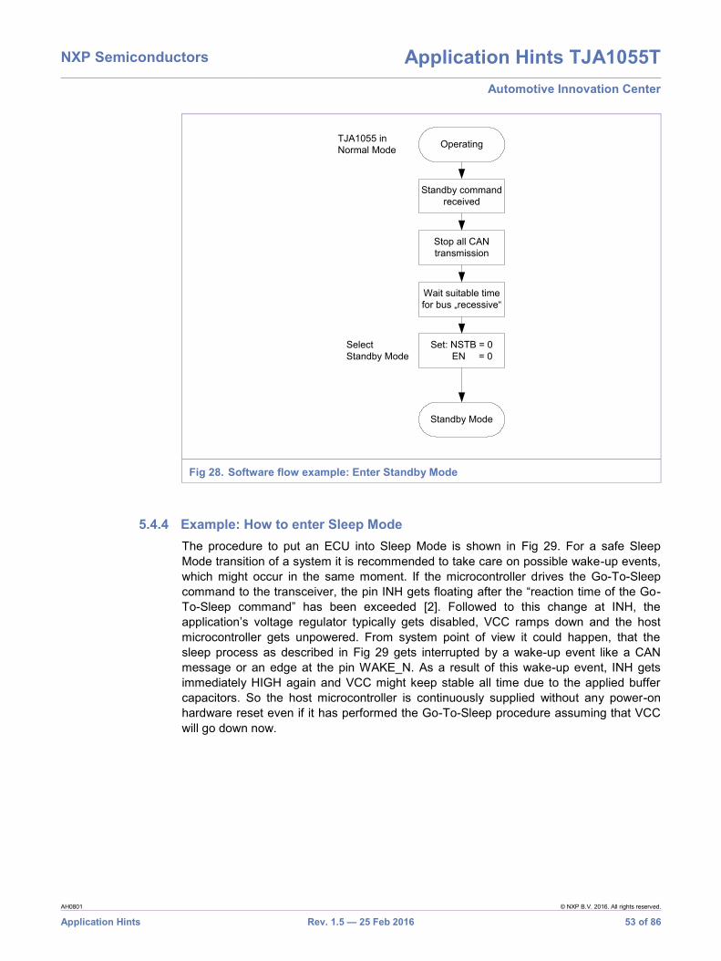
NXP Semiconductors Application Hints TJA1055T Automotive Innovation Center
AH0801 © NXP B.V. 2016. All rights reserved.
Application Hints Rev. 1.5 — 25 Feb 2016 53 of 86
Fig 28. Software flow example: Enter Standby Mode
5.4.4 Example: How to enter Sleep Mode The procedure to put an ECU into Sleep Mode is shown in Fig 29. For a safe Sleep Mode transition of a system it is recommended to take care on possible wake-up events, which might occur in the same moment. If the microcontroller drives the Go-To-Sleep command to the transceiver, the pin INH gets floating after the “reaction time of the Go-To-Sleep command” has been exceeded [2]. Followed to this change at INH, the application’s voltage regulator typically gets disabled, VCC ramps down and the host microcontroller gets unpowered. From system point of view it could happen, that the sleep process as described in Fig 29 gets interrupted by a wake-up event like a CAN message or an edge at the pin WAKE_N. As a result of this wake-up event, INH gets immediately HIGH again and VCC might keep stable all time due to the applied buffer capacitors. So the host microcontroller is continuously supplied without any power-on hardware reset even if it has performed the Go-To-Sleep procedure assuming that VCC will go down now.
Operating
Set: NSTB = 0 EN = 0
Standby commandreceived
Stop all CANtransmission
Wait suitable timefor bus „recessive“
TJA1055 inNormal Mode
Standby Mode
SelectStandby Mode
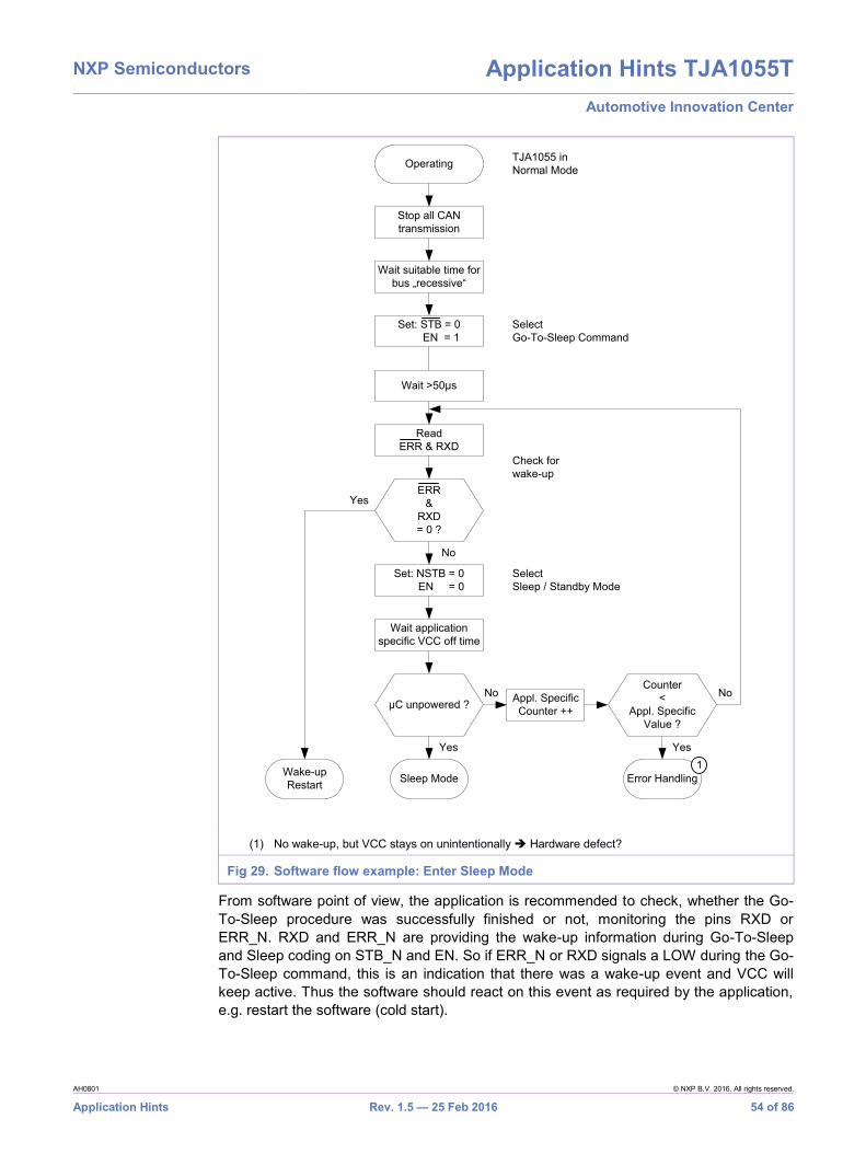
NXP Semiconductors Application Hints TJA1055T Automotive Innovation Center
AH0801 © NXP B.V. 2016. All rights reserved.
Application Hints Rev. 1.5 — 25 Feb 2016 54 of 86
(1) No wake-up, but VCC stays on unintentionally Hardware defect?
Fig 29. Software flow example: Enter Sleep Mode
From software point of view, the application is recommended to check, whether the Go-To-Sleep procedure was successfully finished or not, monitoring the pins RXD or ERR_N. RXD and ERR_N are providing the wake-up information during Go-To-Sleep and Sleep coding on STB_N and EN. So if ERR_N or RXD signals a LOW during the Go-To-Sleep command, this is an indication that there was a wake-up event and VCC will keep active. Thus the software should react on this event as required by the application, e.g. restart the software (cold start).
Wait application specific VCC off time
Operating
Set: STB = 0 EN = 1
Stop all CAN transmission
Wait suitable time for bus „recessive“
TJA1055 in Normal Mode
Select Go-To-Sleep Command
Read ERR & RXD
ERR &
RXD= 0 ?
Error HandlingSleep Mode
Yes
No
Check for wake-up
Yes
No
Wait >50µs
Set: NSTB = 0 EN = 0
Select Sleep / Standby Mode
Counter <
Appl. SpecificValue ?
Appl. Specific Counter ++
Wake-up Restart
µC unpowered ?No
Yes1

NXP Semiconductors Application Hints TJA1055T Automotive Innovation Center
AH0801 © NXP B.V. 2016. All rights reserved.
Application Hints Rev. 1.5 — 25 Feb 2016 55 of 86
6. EMC and ESD
6.1 EMI and EME improvements 6.1.1 Series resistors in TXD and RXD for EME improvement
The interface between µC and transceiver consists of two digital lines TXD and RXD, which are designed to provide sufficient drive capability for all application cases. This might increase the electromagnetic emission of the ECU when the applied signals show fast slops. Optionally it is possible to place a series resistor in the RXD and TXD lines to reduce this emission. This would help to smooth the edges during bit transmissions. But this will also increase the propagation delay, which has to be taken into account. Fig 30 shows the schematic of these optional resistors.
* Optional
Fig 30. Influence of the additional RXD / TXD series resistors to the propagation delay
6.1.2 Common mode choke for improvements of RF-immunity A common mode choke provides high impedance for common mode signals and low impedance for differential data signals. Due to this, common mode signals, either produced by RF noise or by the transceiver itself, get effectively attenuated while passing the choke. In fact, a common mode choke helps to reduce emission and to improve immunity against common mode disturbances. Whether a choke is needed or not depends on the system implementation and on the requirement of the car manufactures. When a common mode choke should be added then it has to be placed between the bus wires and the termination resistors RRTH and RRTL as shown Fig 31. But the choke shall also be placed nearest to the transceiver bus pins. In the following table there are listed the recommended common mode chokes for applications using the TJA1054T or TJA1055T.
Table 19 Recommended common mode chokes for the TJA1054T / TJA1055T Choke typ TJA1054T TJA1055T
100µH YES5 YES
51µH YES YES
5 The stability of the TJA1054T ERR_N output signal at shorts between CANH to GND or CANL to VCC is affected by strong coupling between CANH and CANL.
td td
TJA1055REMC*
RxD
TXD
REMC* VCC
µC + CANController
RxD
VCC
TxD
URXDµC URXDTrx
td - additional time delay caused by the series resistor

NXP Semiconductors Application Hints TJA1055T Automotive Innovation Center
AH0801 © NXP B.V. 2016. All rights reserved.
Application Hints Rev. 1.5 — 25 Feb 2016 56 of 86
The TJA1055T has the potential to build in-vehicle bus systems without chokes. Whether a choke is needed or not finally depends on the specific system implementation like the wiring harness and the symmetry of the two bus lines (matching tolerances of resistors and capacitors).
6.1.3 Bus capacitors for EMI improvements Matching capacitors (in pairs) at CANH and CANL to GND (CH and CL) are frequently used to enhance immunity against electromagnetic interference. Along with the impedance of corresponding noise sources (RF), capacitors at CANH and CANL to GND are forming a RC low-pass filter. Regarding immunity the capacitor value should be as large as possible in order to achieve a low corner frequency. On the other hand, the overall capacitive load and the impedance of the output stage establish a RC low-pass filter for the data signals. Thus the associated corner frequency must be well above the data transmission frequency. This results in a limit for the capacitor value depending on the number of nodes and the data transmission frequency. Notice that capacitors are increasing the signal loop delay due to reducing rise and fall times. At a bit rate of 125kbit/s the capacitor value should not exceed 330pF. Typically, the capacitors are placed between the common mode choke (if applied at all) and the optional ESD clamping diodes as shown in Fig 31.
* Optional (1) Common mode choke (e.g. B82790S513) (2) Capacitors CH = CL = 100pF to 330pF (3) Clamping diodes for ESD protection, e.g. PESD1CAN
Fig 31. CAN circuit for improved EMC behaviour
CommonMode Choke (1)
ESDProtection
PESD1CAN*CH*CL*
RRTL
RRTHTJA1055TJA1055/3
RTL
CANL
CANH
RTH (2)(3)

NXP Semiconductors Application Hints TJA1055T Automotive Innovation Center
AH0801 © NXP B.V. 2016. All rights reserved.
Application Hints Rev. 1.5 — 25 Feb 2016 57 of 86
6.2 ESD protection with PESD1CAN The TJA1055T is designed to withstand Electro Static Discharges (ESD) pulses up to 8kV according to the human body model and 6kV according to the IEC 61000-4-2 at the bus pins CANH, CANL and the termination pins RTL and RTH and thus typically does not need further external protection methods. However, if much higher protection is required, external clamping circuits can be applied to the optionally CANH and CANL line. In Fig 31 the optional external ESD protection is realized with the PESD1CAN at CANH and CANL to GND. The PESD1CAN is provided in small SOT23 SMD plastic package and designed to protect two CAN bus lines from the damage caused by ESD and other transients. The ESD protection diode PESD1CAN is especially designed to fulfill the demands of CAN bus lines. The PESD1CAN offers a very low diode capacitance of typical 11pF. It is recommended to apply the ESD protection circuitry close to the connectors of the ECU as shown in Fig 31.

NXP Semiconductors Application Hints TJA1055T Automotive Innovation Center
AH0801 © NXP B.V. 2016. All rights reserved.
Application Hints Rev. 1.5 — 25 Feb 2016 58 of 86
7. Design Check List
Table 20 Check List for Hard- and Software Development
No Item Comment Check
√ / X
1 VCC Check proper buffering according to 4.2.7.4.
2 VCC Bypass capacitors for the supply pin shall be connected as close as possible to the transceiver pin
3 RXD / ERR_N
Check TJA1055T/3 external pull-up resistors towards the microcontroller supply voltage. See 4.2.4.2 Check TJA1055T regarding pull-up behavior or assigned µC input ports. See 4.2.4.3.
4 RTH RTL
Check for proper system termination, total termination has to be about 100 Ohms, a single node’s termination is recommended not to exceed approx. 6k especially at long stubs.
5 INH INH is a VBAT related pin (open drain towards VBAT) and thus is NOT suitable to be connected directly to an input port of a microcontroller without external clamping or level adaptation. The continuous drive capability should be 1mA.
6 WAKE_N WAKE_N is a VBAT related pin (internal pull-up to VBAT) and thus is NOT suitable to be connected directly to a microcontroller port without external clamping or level adaptation.
7 WAKE_N The output drive capability of the integrated pull-up to VBAT is intended to keep this pin on a defined level in case of an open circuit condition due to a failure on the PCB. This internal pull-up of some µA is NOT suitable to be driven directly by external circuitry like open collector bipolar transistors. The leakage current of such a transistor might be enough to cause a continuous LOW level at WAKE thus allowing no edges for wake-up anymore. An external default load or a push-pull driver is recommended here if this pin is used for local wake-up sources. (e.g. pull-up resistor to BAT ... )
8 WAKE_N An unused pin WAKE should not be left open due to immunity issues. Especially if some optional wiring is connected to this pin, this wire represents a potential antenna for environmental noise. Due to the integrated pull-up towards VBAT followed by an analogue filter, unwanted wake-up’s are never observed for an open pin WAKE even with EMC load on it. Nevertheless it is recommended to connect an unused pin WAKE with the pin BAT of the transceiver for safety reasons. Pulling to VCC or GND permanently is NOT recommended because this would result in a continuous current flow out of the internal pull-up to BAT.

NXP Semiconductors Application Hints TJA1055T Automotive Innovation Center
AH0801 © NXP B.V. 2016. All rights reserved.
Application Hints Rev. 1.5 — 25 Feb 2016 59 of 86
No Item Comment Check
√ / X
9 WAKE_N If the pin WAKE is directly connected to a wake-up source with separate GND connection (like an external switch to GND outside of the PCB) a series protection resistor is recommended as shown within the application diagram. This series resistor is used to limit the maximum current flowing in case the entire control unit has lost its GND connection. In this case, all the application current would flow through the external wake-up switch to GND. This may damage the transceiver. See also chapter 4.2.2.
10 Choke When a common mode choke is used, it shall be placed as close as possible to the transceiver bus pins CANH and CANL
11 PCB The PCB tracks for the bus signals CANH and CANL shall be routed close together in a symmetrical way. Its length should be as short as possible to the connector.
12 PCB CANL and CANH should be routed in parallel.
13 PCB Distance from microcontroller to the transceiver should be as short as possible.
14 PCB Distance from transceiver to the connector should be as short as possible.
15 PCB Connection of TXD, RXD, STB and EN to the host microcontroller should be in parallel to ground in order to guarantee a common reference level.
16 PCB Ground planes should be used whenever possible. For multilayer printed circuit boards, use ground vias.
17 ESD Optional suppressor diodes or varistors for ESD protection shall be connected close to the ECU connector bus terminal.
18 PESD1CAN Place the protection device as close as possible to the input terminal or connector of the ECU.
19 Software Check whether the Go-to-Sleep time td(SLEEP)MAX
20 Software Check for late wake-up. It could happen that the Go-to-Sleep procedure is interrupted by a wake-up event (e.g. CAN message). As a result of this wake-up event the INH pin is set immediately high again and VCC night keep stable all time due to applied buffer capacitors.
21 Software Check, whether EN pin is actively set low after exceeding the Go-to-Sleep time td(SLEEP)MAX with VCC > 4V (see 5.1.4)
22 Software Check, whether ERR_N is connected to an Interrupt source of the host microcontroller. It is not recommended to force Interrupts based on the ERR_N signal during operation, because that may cause quite some interrupt load depending on the bus fault condition. ERR_N may toggle with each CAN frame on the bus lines at bus interruptions.

NXP Semiconductors Application Hints TJA1055T Automotive Innovation Center
AH0801 © NXP B.V. 2016. All rights reserved.
Application Hints Rev. 1.5 — 25 Feb 2016 60 of 86
8. FAQs
8.1 There was a wake-up event during the “Goto Sleep” procedure. The pin WAKE is connected to the local 5V supply, which is controlled by the pin INH of the transceiver. In this case the Sleep Mode was entered successfully and the pin INH becomes floating. As a result of this the 5V supply is switched off -> VCC drops down. These forces an edge at WAKE_N and the device wakes up again. If WAKE_N is not used within the application it should be connected directly to the pin BAT of the transceiver (see also chapter 5.4.4).
There is an external CAN-Tool connected to the network and the GND connection between the PC and the application is missing. The floating bus wires are forcing wake-up events for the application.
The GND connection between separate powered nodes is lost. Result as discussed above.
8.2 System operates in Single Wire Mode all time There is still a termination resistor between the bus wires present as known from the high-speed physical layer. E.g. a CAN tool with high-speed transceiver and termination is connected. The fault tolerant physical layer has NO termination resistor between the wires but a distributed termination at all nodes connected between pins CANH and RTH, CANL and RTL. See also chapter 9.1.
8.3 System does not wake-up, even if there is bus activity For bus wake-up a CAN message with 5 consecutive dominant bits are required. This guarantees the minimum dominant time of 38us needed to wake-up the transceiver. Depending on the bit rate even messages with less than 5 consecutive dominant bits are sufficient to achieve the 38us dominant requirement.
Systems using the Standby Mode keeping the VCC supply alive are usually waked up with a dominant edge at RXD or ERR_N respectively. Depending on the uC hardware and software, this edge might be lost for the uC with the result that the uC enters its low-power mode (Stop Mode) with RXD and ERR_N continuously set LOW (wake-up). There are no further edges and thus the uC does not wake up. For these applications it is recommended to support a level sensitive wake-up or to make sure that all edges are recognized independently from software actions.
8.4 Transceiver is damaged when external tools are connected Since PC’s and other external equipment is typically supplied from the AC power supply while the car is isolated and supplied from a battery, there might be a very high voltage difference between both CAN networks. It is recommended to make sure that the GND

NXP Semiconductors Application Hints TJA1055T Automotive Innovation Center
AH0801 © NXP B.V. 2016. All rights reserved.
Application Hints Rev. 1.5 — 25 Feb 2016 61 of 86
line between external stuff and the car is connected first, followed by the bus lines in order to have the same reference level.
8.5 CAN tool cannot communicate with certain application Often a CAN tool is used to simulate the entire car environment for functional verifications of a single application. The problem is that the CAN tool does not provide the same termination resistance as present in the car’s environment. In order to get this set-up running the CAN tool has to be supplied with a lower internal termination. It is recommended to replace the existing resistors inside of the CAN tool with e.g. 500 Ohms (the minimum allowed termination per transceiver) for test purposes. The total termination of all nodes should still keep above or equal to 100 Ohms.

NXP Semiconductors Application Hints TJA1055T Automotive Innovation Center
AH0801 © NXP B.V. 2016. All rights reserved.
Application Hints Rev. 1.5 — 25 Feb 2016 62 of 86
9. Appendix
9.1 Bus Termination 9.1.1 Dimensioning of the bus termination resistors
The fault tolerant CAN transceiver TJA1055T is designed to deliver optimum system behavior at a total termination resistance of 100 Ohm at the line CANH as well as CANL. Because the termination of the fault tolerant system is distributed all over the network, each of the transceivers has to deliver only a part of the total termination of 100 Ohm. So depending on the overall system size the single nodes local termination resistors have to be adjusted to deliver optimum system performance.
Fig 32. Example network with 5 nodes
The termination resistors are connected to the corresponding pins RTH and RTL of the transceivers within each control unit. It is not required that each transceiver in the system has the same termination resistor value. In total the termination should result in 100 Ohm per bus line. It is not recommended to terminate the entire system lower than 100 Ohm since the CAN output drivers are optimized for 100 Ohm load. A more low-ohmic termination might result in less GND shift capability during bus faults due to smaller signal amplitude.
The minimum termination resistor value allowed per transceiver is 500 Ohm due to the driving capability of the pins RTL and RTH. So within systems with less than 4 transceivers it is not possible to achieve the termination optimum of 100 Ohm. In practice this is typically no problem because such “small” systems will have less bus cable lengths compared to bigger networks and thus have no problem with a higher total termination resistances.
It is recommended not to exceed approximately a 6kOhm termination resistance at a single transceiver especially using long stubs in order to provide good system performance in case of interrupted bus wires.
9.1.1.1 Variable System Size and Optional Nodes
In case of variable system sizes with optional nodes it is recommended to achieve the total termination resistance close to 100Ohm provided by the standard nodes, which are always present. The optional nodes should have the higher termination resistances then. In order to keep tolerance against open wire conditions even for longer stub lines it is recommended not to exceed approximately 6kOhm for the optional nodes.
500500 500500
TJA1055T
500500 500500 500500
TJA1055T TJA1055T TJA1055T TJA1055T

NXP Semiconductors Application Hints TJA1055T Automotive Innovation Center
AH0801 © NXP B.V. 2016. All rights reserved.
Application Hints Rev. 1.5 — 25 Feb 2016 63 of 86
Example calculation
The entire example system has 15 nodes in total, 5 nodes of this system are equipped optionally if required:
Termination of the 10 standard nodes: 1.2kOhm per node
Termination of the 5 optional nodes: 3kOhm per node
Total system termination (10 standard nodes only):
o 1.2 kOhm / 10 = 120 Ohm (close to 100)
Total system termination (10 standard nodes and 5 optional nodes):
o (3 kOhm / 5) parallel to 120 Ohm = 100 Ohm
9.1.1.2 Distribution of the termination resistors
There is no general rule how to distribute the termination within the network, but a rule of thumb is:
“The longer the cable stub, the lower the local termination should be.”
It is recommended to keep the local time constant of a stub line below 1/6th of the bit time.
Table 21 Example values for termination resistor calculation Symbol Description Value
L Length of cable stub 5m
C’ Line capacitance 120pF/m
CECU Capacitance of the ECU 100pF
tBIT Minimum bit duration (for 125kbit/s) 8µs
Capacitance: C = L * C’ + CECU = 5m * 120pF/m + 100pF = 700pF
Local time constant: 1/6th = R * C
R = / (6*C) = 8µs / 4200pF
Rt < 1900 Ohm
9.1.2 Tolerances of Bus Termination Resistors The symmetry of the termination resistors within a single node has a major impact to the systems EME (Electro Magnetic Emission) behavior. Thus it is important to have well matched termination resistors within each control unit. This means that the RTH resistor should have exactly the same value as the RTL resistor within one control unit in order to get the same time constant on each bus wire during signal transitions. Two different control units might have completely different termination values (see chapter 9.1.1.1).

NXP Semiconductors Application Hints TJA1055T Automotive Innovation Center
AH0801 © NXP B.V. 2016. All rights reserved.
Application Hints Rev. 1.5 — 25 Feb 2016 64 of 86
The principle to achieve a good EME performance is that the differential signal on the bus wires eliminates any emission due to compensation effects if both CAN wires are carrying exactly the same signal, but with inverse polarities.
Here the transceiver can only provide a perfect symmetry for the dominant transitions by design. The recessive transitions are mainly driven by the termination resistors and by the network cables. So not only the transceiver’s output drivers have an impact to the EME performance but also the termination and the cable symmetry.
It is recommended to provide termination resistor accuracy (RTH compared to RTL) within the same node of maximum 1% or lower. Also the bus cable has to be at least a twisted pair cable in order to achieve a symmetrical capacitive load for both bus wires resulting in a good EMC performance.
It is obvious that also the layout of printed circuit boards has a significant impact to the EMC behavior if the CAN lines have different capacitive loads due to different wire lengths.
NXP Semiconductors Application Hints TJA1055T Automotive Innovation Center
AH0801 © NXP B.V. 2016. All rights reserved.
Application Hints Rev. 1.5 — 25 Feb 2016 65 of 86
9.1.3 Power Dissipation of Termination Resistors 9.1.3.1 Summary
The bus termination resistors RT being connected to the fault tolerant transceiver are recommended to withstand the power dissipation (@ RT > 1000 Ohms) of 31,7mW. The following chapters are discussing this issue in more detail.
9.1.3.2 Average power dissipation, no bus failures
In order to dimension the power dissipation of the termination resistors connected to pins RTH and RTL, the average power dissipation between dominant and recessive bits has to be taken into account. Additionally a worst-case ground offset of the certain module has an impact.
CAN frames are assumed to have a ratio of dominant bits in the range of 0.75 worst-case because of stuffing and fixed recessive frame segments. Thus the average power dissipation is calculated as follows:
Pavg = 0.75 * (Vcc + VGND) 2 / RT
Hint: For this calculation it is assumed that RTL is pulled to VCC while this ECU has 1,5V GND shift compared to the rest of the system and the bus driver of the sending node is able to pull CANL towards the real system GND without any drop (super worst case).
Example calculation, average power dissipation
Assumption: RT = 1000 Ohm
Pavg = 0.75 * (5V + 1,5V) 2 / 1000 Ohm = 31.7 mW
9.1.3.3 Maximum continuous power dissipation (single bus failure)
The maximum continuous current flows in case CANH has a short to VCC or BAT at the maximum detection threshold of 1.85V.
Pcont = (Vdet max) 2 / RT
Hint: If CANH would be pulled to a higher voltage, the bus failure management would disable RTH and thus interrupt the RTH current.
Example calculation, maximum continuous power dissipation
Assumption: RT = 1000 Ohm, connected to RTH
Pcont = (1.85 V) 2 / 1000 Ohms = 3.4 mW
9.1.3.4 Maximum peak power dissipation (single bus failure)
A peak current will flow in case of short circuits of CANH to VBAT. After the device maximum specific detection time of 8ms, the bus failure detector will switch off the bias on RTH. Thus this peak current does only flow for a short time.
Ppeak = VBAT2 / RT ( t < tdet_HBAT )
Example calculation, maximum peak power dissipation
Assumptions: RT = 1000 Ohms, VBAT = 27V
Ppeak = (27 V)2 / 1000 Ohms = 730 mW for less than 8 ms

NXP Semiconductors Application Hints TJA1055T Automotive Innovation Center
AH0801 © NXP B.V. 2016. All rights reserved.
Application Hints Rev. 1.5 — 25 Feb 2016 66 of 86
Because this peak current does flow for a very short time only, it typically has no relevance for dimensioning the termination resistors. Most important is the average power dissipation for the TJA1055T (31,7 mW) since this is the worst-case condition.
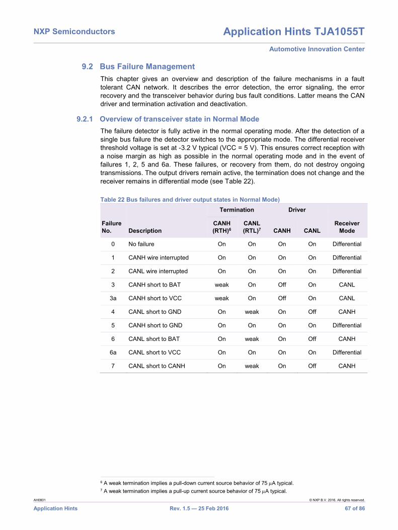
NXP Semiconductors Application Hints TJA1055T Automotive Innovation Center
AH0801 © NXP B.V. 2016. All rights reserved.
Application Hints Rev. 1.5 — 25 Feb 2016 67 of 86
9.2 Bus Failure Management This chapter gives an overview and description of the failure mechanisms in a fault tolerant CAN network. It describes the error detection, the error signaling, the error recovery and the transceiver behavior during bus fault conditions. Latter means the CAN driver and termination activation and deactivation.
9.2.1 Overview of transceiver state in Normal Mode The failure detector is fully active in the normal operating mode. After the detection of a single bus failure the detector switches to the appropriate mode. The differential receiver threshold voltage is set at -3.2 V typical (VCC = 5 V). This ensures correct reception with a noise margin as high as possible in the normal operating mode and in the event of failures 1, 2, 5 and 6a. These failures, or recovery from them, do not destroy ongoing transmissions. The output drivers remain active, the termination does not change and the receiver remains in differential mode (see Table 22).
Table 22 Bus failures and driver output states in Normal Mode)
Failure No. Description
Termination Driver
Receiver Mode
CANH (RTH)6
CANL (RTL)7 CANH CANL
0 No failure On On On On Differential
1 CANH wire interrupted On On On On Differential
2 CANL wire interrupted On On On On Differential
3 CANH short to BAT weak On Off On CANL
3a CANH short to VCC weak On Off On CANL
4 CANL short to GND On weak On Off CANH
5 CANH short to GND On On On On Differential
6 CANL short to BAT On weak On Off CANH
6a CANL short to VCC On On On On Differential
7 CANL short to CANH On weak On Off CANH
6 A weak termination implies a pull-down current source behavior of 75 A typical. 7 A weak termination implies a pull-up current source behavior of 75 A typical.
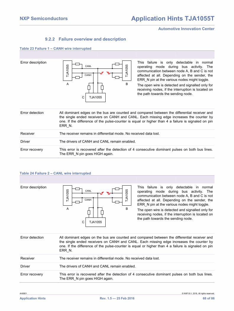
NXP Semiconductors Application Hints TJA1055T Automotive Innovation Center
AH0801 © NXP B.V. 2016. All rights reserved.
Application Hints Rev. 1.5 — 25 Feb 2016 68 of 86
9.2.2 Failure overview and description
Table 23 Failure 1 – CANH wire interrupted
Error description
This failure is only detectable in normal operating mode during bus activity. The communication between node A, B and C is not affected at all. Depending on the sender, the ERR_N pin at the various nodes might toggle. The open wire is detected and signalled only for receiving nodes, if the interruption is located on the path towards the sending node.
Error detection All dominant edges on the bus are counted and compared between the differential receiver and the single ended receivers on CANH and CANL. Each missing edge increases the counter by one. If the difference of the pulse-counter is equal or higher than 4 a failure is signaled on pin ERR_N.
Receiver The receiver remains in differential mode. No received data lost.
Driver The drivers of CANH and CANL remain enabled.
Error recovery This error is recovered after the detection of 4 consecutive dominant pulses on both bus lines. The ERR_N pin goes HIGH again.
Table 24 Failure 2 – CANL wire interrupted
Error description
This failure is only detectable in normal operating mode during bus activity. The communication between node A, B and C is not affected at all. Depending on the sender, the ERR_N pin at the various nodes might toggle. The open wire is detected and signalled only for receiving nodes, if the interruption is located on the path towards the sending node.
Error detection All dominant edges on the bus are counted and compared between the differential receiver and the single ended receivers on CANH and CANL. Each missing edge increases the counter by one. If the difference of the pulse-counter is equal or higher than 4 a failure is signaled on pin ERR_N.
Receiver The receiver remains in differential mode. No received data lost.
Driver The drivers of CANH and CANL remain enabled.
Error recovery This error is recovered after the detection of 4 consecutive dominant pulses on both bus lines. The ERR_N pin goes HIGH again.
CANH
CANLTJ
A105
5
A B
C TJA1055
TJA1
055
CANH
CANL
TJA1
055
TJA1
055
A B
C TJA1055

NXP Semiconductors Application Hints TJA1055T Automotive Innovation Center
AH0801 © NXP B.V. 2016. All rights reserved.
Application Hints Rev. 1.5 — 25 Feb 2016 69 of 86
Table 25 Failure 3 – CANH short-circuited to battery
Error description
This failure is detectable in all operating modes. The CANH line is clamped to VBAT level preventing all communication on that line in the whole network. The transceiver switches to single-wire communication on CANL. Pin ERR_N signals an error as a continuous LOW signal.
Error detection Failure 3 is detected via comparators connected to the CANH and the differential bus comparator. The CANH to BAT short is detected in a two-step approach. If the CANH bus line exceeds a certain voltage level, the differential comparator signals a continuous dominant condition. After a first time-out the transceiver switches to single-wire operation through CANH. If the CANH bus line still exceeds the CANH dominant voltage for a second time-out, the TJA1055T switches to CANL operation; the CANH driver is switched off and the RTH bias changes to the pull-down current source.
Receiver The receiver switches to CANL. The failure detection might cause a CAN error frame.
Driver The driver of CANH is disabled.
Error recovery This error is recovered if the differential and single wire comparators show a recessive level for a certain time. The ERR_N pin goes HIGH again.
Table 26 Failure 3a – CANH short-circuited to VCC
Error description
This failure is detectable in all operating modes. The CANH line is clamped to VCC level preventing all communication on that line in the whole network. The transceiver switches to single-wire communication on CANL. Pin NERR signals an error as a continuous LOW signal.
Error detection Failure 3a is detected via comparators connected to the CANH and the differential bus comparator. The CANH to VCC short is detected in a two-step approach. If the CANH bus line exceeds a certain voltage level, the differential comparator signals a continuous dominant condition. After a first time-out the transceiver switches to single-wire operation through CANH. If the CANH bus line still exceeds the CANH dominant voltage for a second time-out, the TJA1055T switches to CANL operation; the CANH driver is switched off and the RTH bias changes to the pull-down current source.
Receiver The receiver switches to CANL. The failure detection might cause a CAN error frame.
Driver The driver of CANH is disabled.
B
CANH
CANL
TJA1
055
A
C TJA1055
BATT
TJA1
055
B
CANH
CANL
TJA1
055
A
C TJA1055
VCC
TJA1
055

NXP Semiconductors Application Hints TJA1055T Automotive Innovation Center
AH0801 © NXP B.V. 2016. All rights reserved.
Application Hints Rev. 1.5 — 25 Feb 2016 70 of 86
Error recovery . This error is recovered if the differential and single wire comparators show a recessive level for a certain time. The ERR_N pin goes HIGH again.
Table 27 Failure 4 – CANL short-circuited to GND
Error description
This failure is detectable in all operating modes. The CANL line is clamped to GND level preventing all communication on that line in the whole network. For CANL the GND level is the dominant state. Communication is only possible on CANH. The nodes A, B and C switch into single wire mode. Pin ERR_N signals the error as a continuous LOW signal.
Error detection Failure 4 results in a permanent dominant level on the differential comparator. After a time-out the CANL driver is switched off and the RTL bias changes to the pull-up current source. Reception continues by switching to the single-wire mode via pin CANH.
Receiver The receiver switches to CANH. The failure detection might cause a CAN error frame.
Driver The driver of CANL is disabled.
Error recovery This error is recovered If the differential voltage remains below the recessive threshold level for a certain period of time; reception and transmission switch back to the differential mode. The ERR_N pin goes HIGH again.
B
CANH
CANL
TJA1
055
A
C TJA1055
GND
TJA1
055

NXP Semiconductors Application Hints TJA1055T Automotive Innovation Center
AH0801 © NXP B.V. 2016. All rights reserved.
Application Hints Rev. 1.5 — 25 Feb 2016 71 of 86
Table 28 Failure 5 – CANH short-circuited to GND
Error description This failure is detectable only during communication in normal mode. CANH line is clamped to GND level preventing all communication on that line in the whole network. GND is the recessive state of CANH. If the transceiver receives a dominant bit via the differential comparator but not on CANH the internal error counter is increased by one. The communication between node A, B and C is not affected at all. Pin NERR signals the error as a continuous LOW signal.
Error detection All dominant edges on the bus are counted and compared between the differential signal, CANH and CANL. Each missing edge increases the counter. If the difference of the pulse-counter is equal or higher than 4 a failure is signaled on pin ERR_N.
Receiver The receiver stays in differential mode; no ongoing transmission is lost.
Driver The output driver remains active.
Error recovery This error is recovered after the detection of 4 consecutive dominant pulses on both bus lines. The ERR_N pin goes HIGH again.
Table 29 Failure 6 – CANL short-circuited to battery
Error description
This failure is detectable in normal mode. The CANL line is clamped to VBAT level preventing all communication on that line in the whole network. The transceiver switches into single-wire communication on CANH. Pin ERR_N signals an error as a continuous LOW signal.
Error detection Failure 6 is detected via comparator connected to CANL bus line. If the CANL bus line exceeds a certain voltage level close to the battery voltage for a certain period of time the transceiver switches to single-wire operation through CANH.
Receiver The receiver switches to CANH. The failure detection might cause a CAN error frame.
Driver The CANL driver switches off.
Error recovery This error is recovered automatically as soon as the voltage threshold of the CANL comparator falls below the detection level for a defined time. The ERR_N pin goes HIGH again.
B
CANH
CANL
TJA1
055
A
C TJA1055
GND
TJA1
055
B
CANH
CANL
TJA1
055
A
C TJA1055
BATT
TJA1
055
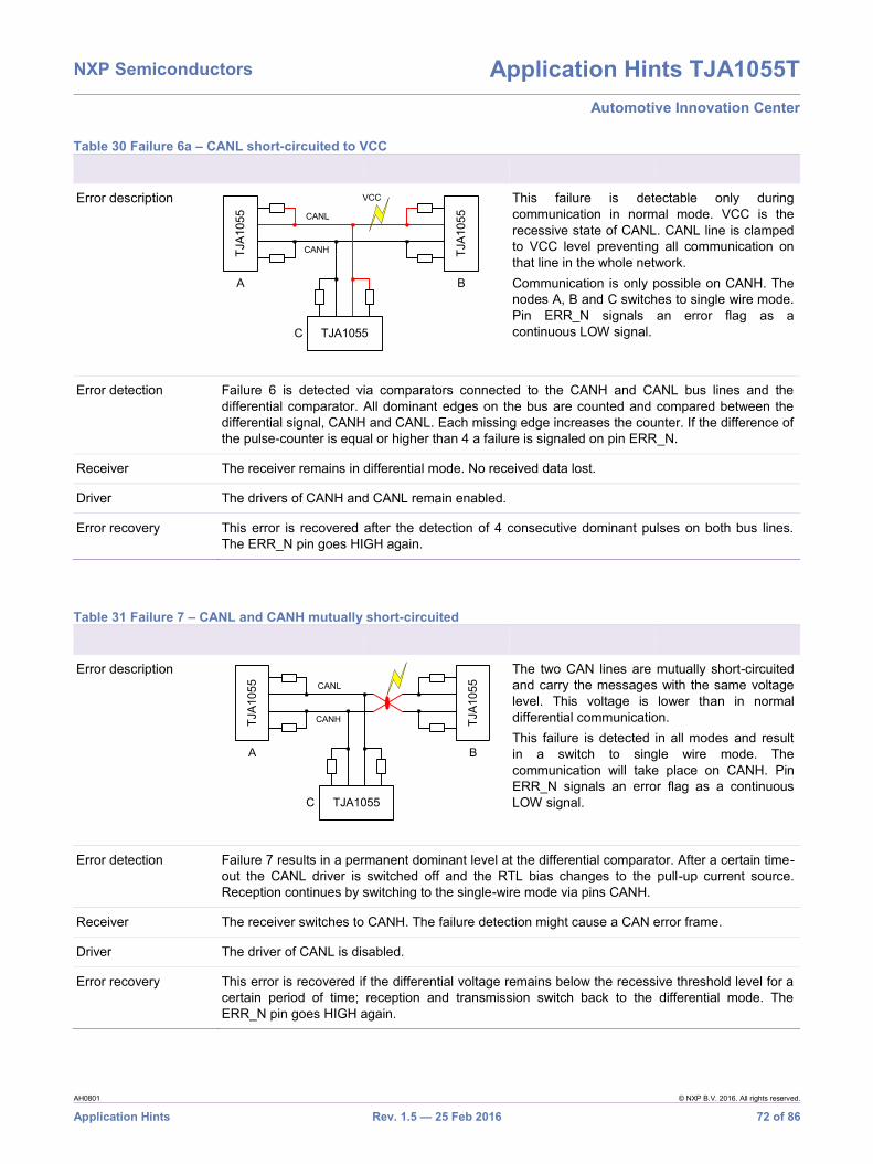
NXP Semiconductors Application Hints TJA1055T Automotive Innovation Center
AH0801 © NXP B.V. 2016. All rights reserved.
Application Hints Rev. 1.5 — 25 Feb 2016 72 of 86
Table 30 Failure 6a – CANL short-circuited to VCC
Error description
This failure is detectable only during communication in normal mode. VCC is the recessive state of CANL. CANL line is clamped to VCC level preventing all communication on that line in the whole network. Communication is only possible on CANH. The nodes A, B and C switches to single wire mode. Pin ERR_N signals an error flag as a continuous LOW signal.
Error detection Failure 6 is detected via comparators connected to the CANH and CANL bus lines and the differential comparator. All dominant edges on the bus are counted and compared between the differential signal, CANH and CANL. Each missing edge increases the counter. If the difference of the pulse-counter is equal or higher than 4 a failure is signaled on pin ERR_N.
Receiver The receiver remains in differential mode. No received data lost.
Driver The drivers of CANH and CANL remain enabled.
Error recovery This error is recovered after the detection of 4 consecutive dominant pulses on both bus lines. The ERR_N pin goes HIGH again.
Table 31 Failure 7 – CANL and CANH mutually short-circuited
Error description
The two CAN lines are mutually short-circuited and carry the messages with the same voltage level. This voltage is lower than in normal differential communication. This failure is detected in all modes and result in a switch to single wire mode. The communication will take place on CANH. Pin ERR_N signals an error flag as a continuous LOW signal.
Error detection Failure 7 results in a permanent dominant level at the differential comparator. After a certain time-out the CANL driver is switched off and the RTL bias changes to the pull-up current source. Reception continues by switching to the single-wire mode via pins CANH.
Receiver The receiver switches to CANH. The failure detection might cause a CAN error frame.
Driver The driver of CANL is disabled.
Error recovery This error is recovered if the differential voltage remains below the recessive threshold level for a certain period of time; reception and transmission switch back to the differential mode. The ERR_N pin goes HIGH again.
CANH
CANL
TJA
1055
A B
C TJA1055
TJA
1055
B
CANH
CANL
TJA1
055
A
C TJA1055
VCC
TJA1
055

NXP Semiconductors Application Hints TJA1055T Automotive Innovation Center
AH0801 © NXP B.V. 2016. All rights reserved.
Application Hints Rev. 1.5 — 25 Feb 2016 73 of 86
9.3 Pin FMEA This chapter provides a FMEA (Failure Mode and Effect Analysis) for the typical failure situations, when dedicated pins of the TJA1055T are short-circuited to supply voltages like VBAT, VCC, GND or to neighboured pins or are simply left open. The individual failures are classified, due to their corresponding effects on the transceiver and bus communication.
Table 32 Classification of failure effects Class Effects
A - Damage to transceiver - Bus may be effected
B - No damage to transceiver - No bus communication possible
C - No damage to transceiver - Bus communication possible - Corrupted node excluded from communication
D - No damage to transceiver - Bus communication possible - Reduced functionality of transceiver
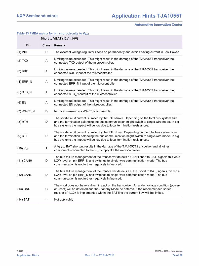
NXP Semiconductors Application Hints TJA1055T Automotive Innovation Center
AH0801 © NXP B.V. 2016. All rights reserved.
Application Hints Rev. 1.5 — 25 Feb 2016 74 of 86
Table 33 FMEA matrix for pin short-circuits to VBAT
Pin
Short to VBAT (12V…40V)
Class Remark
(1) INH D The external voltage regulator keeps on permanently and avoids saving current in Low Power.
(2) TXD A Limiting value exceeded. This might result in the damage of the TJA1055T transceiver the connected TXD output of the microcontroller.
(3) RXD A Limiting value exceeded. This might result in the damage of the TJA1055T transceiver the connected RXD input of the microcontroller.
(4) ERR_N A Limiting value exceeded. This might result in the damage of the TJA1055T transceiver the connected ERR_N input of the microcontroller.
(5) STB_N A Limiting value exceeded. This might result in the damage of the TJA1055T transceiver the connected STB_N output of the microcontroller.
(6) EN A Limiting value exceeded. This might result in the damage of the TJA1055T transceiver the connected EN output of the microcontroller.
(7) WAKE_N D No local wake-up via WAKE_N is possible.
(8) RTH D The short-circuit current is limited by the RTH driver. Depending on the total bus system size and the termination balancing the bus communication might switch to single-wire mode. In big bus systems the impact will be low due to local termination resistances.
(9) RTL D The short-circuit current is limited by the RTL driver. Depending on the total bus system size and the termination balancing the bus communication might switch to single-wire mode. In big bus systems the impact will be low due to local termination resistances.
(10) VCC A A VCC to BAT shortcut results in the damage of the TJA1055T transceiver and all other components connected to the VCC supply like the microcontroller.
(11) CANH D The bus failure management of the transceiver detects a CANH short to BAT, signals this via a LOW level on pin ERR_N and switches to single-wire communication mode. The bus communication is not further negatively influenced.
(12) CANL D The bus failure management of the transceiver detects a CANL short to BAT, signals this via a LOW level on pin ERR_N and switches to single-wire communication mode. The bus communication is not further negatively influenced.
(13) GND C The short does not have a direct impact on the transceiver. An under voltage condition (power-on reset) will be detected and the Standby Mode be entered. If the recommended series resistor of 1…2k is implemented within the BAT line the current flow will be limited.
(14) BAT - Not applicable

NXP Semiconductors Application Hints TJA1055T Automotive Innovation Center
AH0801 © NXP B.V. 2016. All rights reserved.
Application Hints Rev. 1.5 — 25 Feb 2016 75 of 86
Table 34 FMEA matrix for pin short-circuits to VCC
Pin
Short to VCC (5V)
Class Remark
(1) INH D With a voltage regulator connected to pin INH, this one might stay active forever, depending on its input threshold. If no voltage regulator is connected to the INH pin, the INH to VCC current is limited internally of the TJA1055T.
(2) TXD C The transmission of messages is not possible anymore. The reception of messages is not affected.
(3) RXD B
The CAN controller will see a permanently „free“ bus and might as a result launch messages with random timing. This can lead to a globally corrupted CAN bus communication. The used software can prevent such a system wide problem by monitoring back the CAN controller’s behaviour.
(4) ERR_N D A bus failure diagnosis is not possible.
(5) STB_N D No Sleep Mode possible. The system can switch between Normal, Standby and Power-on Standby only
(6) EN D The Power-on Standby Mode is not available.
(7) WAKE_N D Internally of the TJA1055T the weak current source from WAKE_N to BAT is protecting itself by a current limitation. If the VCC supply gets disabled in Sleep Mode this might cause a wake-up starting the VCC supply again.
(8) RTH D The short-circuit current is limited by the RTH driver. Depending on the total bus system size and the termination balancing the bus communication might switch to single-wire mode. In big bus systems the impact will be significantly low due to local termination resistances.
(9) RTL D VCC is the nominal driver value for the RTL pin. Consequently the bus failure management gets not affected.
(10) VCC - Not applicable
(11) CANH D The bus failure management of the transceiver detects a CANH short to VCC, signals this via a LOW level on pin ERR_N and switches to single-wire communication mode. The bus communication is not further negatively influenced.
(12) CANL D The bus failure management of the transceiver detects a CANL short to VCC, signals this via a LOW level on pin ERR_N and switches to single-wire communication mode. The bus communication is not further negatively influenced.
(13) GND C
The short does not have a direct impact on the transceiver. The external voltage regulator might become overloaded and be switched off. Hence the transceiver detects a low VCC supply and gets into a “Forced Standby Mode”, similar to switching STB_N and EN to LOW. CAN communication is not longer possible. The problem only affects the local ECU.
(14) BAT A A BAT to VCC shortcut results in the damage of the TJA1055T transceiver and all other components connected to the VCC supply like the microcontroller.

NXP Semiconductors Application Hints TJA1055T Automotive Innovation Center
AH0801 © NXP B.V. 2016. All rights reserved.
Application Hints Rev. 1.5 — 25 Feb 2016 76 of 86
Table 35 FMEA matrix for pin short-circuits to GND
Pin
Short to GND
Class Remark
(1) INH C With a voltage regulator connected to pin INH, this one will stay off permanently. If no voltage regulator is connected to the INH pin, the INH to GND current is limited internally of the TJA1055T.
(2) TXD C The TXD dominant timer makes sure that the bus is not clamped dominant forever. As a result the failure stays local, since no transmission of messages from this node is possible. The reception of messages is not affected.
(3) RXD C The CAN controller will see a permanently “locked” bus and thus never start with CAN communication. The problem only affects the local ECU.
(4) ERR_N D The software assumes a bus failure condition and tracks this within a possible diagnosis system.
(5) STB_N C The “Goto Sleep” command will be forced to the transceiver, if the microcontroller’s port HIGH level is weaker than the STB_N pin’s LOW driver (high probability) and the EN pin is set HIGH. As a result the transceiver will enter the Low Power Mode and disable the application.
(6) EN C The system is permanently in Standby Mode. No communication is possible. The transceiver requires only low current.
(7) WAKE_N D Internally of the TJA1055T the weak current source from WAKE_N to BAT is protecting itself by a current limitation. As a result of the shortcut no wake-up via WAKE_N is possible.
(8) RTH D GND is the nominal driver value for the RTH pin. Consequently the bus failure management gets not affected.
(9) RTL D The short-circuit current is limited by the RTL driver. Depending on the total bus system size and the termination balancing the bus communication might switch to single-wire mode. In big bus systems the impact will be low due to local termination resistances.
(10) VCC C
The short does not have a direct impact on the transceiver. The external voltage regulator might become overloaded and be switched off. Hence the transceiver detects a low VCC supply and gets into a “Forced Standby Mode”, similar to switching STB_N and EN to LOW. CAN communication is not longer possible. The problem only affects the local ECU.
(11) CANH D The bus failure management of the transceiver detects a CANH short to GND, signals this via a LOW level on pin ERR_N and switches to single-wire communication mode. The bus communication is not further negatively influenced.
(12) CANL D The bus failure management of the transceiver detects a CANL short to GND, signals this via a LOW level on pin ERR_N and switches to single-wire communication mode. The bus communication is not further negatively influenced.
(13) GND - Not applicable
(14) BAT C The short does not have a direct impact on the transceiver. An under voltage condition (power-on reset) will be detected and the Standby Mode be entered. If the recommended series resistor of 1…2k is implemented within the BAT line the current flow will be limited.

NXP Semiconductors Application Hints TJA1055T Automotive Innovation Center
AH0801 © NXP B.V. 2016. All rights reserved.
Application Hints Rev. 1.5 — 25 Feb 2016 77 of 86
Table 36 FMEA matrix for open pins
Pin
Open
Class Remark
(1) INH C With a voltage regulator connected to pin INH, this one will not start and the ECU will stay in Low Power Mode. If no voltage regulator is connected to the INH pin, no problem occurs.
(2) TXD C The transmission of messages is not possible anymore. The reception of messages is not affected.
(3) RXD C The CAN controller gets no feedback from the bus while transmitting and runs BUS-OFF within a short time. The problem only affects the local ECU once bus off is achieved.
(4) ERR_N D A bus failure diagnosis is not possible.
(5) STB_N C The internal pull-down source of the transceiver makes sure that the STB_N pin internally is LOW. The “Goto Sleep” command will be forced to the transceiver, if the EN pin is set HIGH. As a result the transceiver will enter the Low Power Mode and disable the application.
(6) EN C The internal pull-down source of the transceiver makes sure that the EN pin internally is LOW. Consequently the system is permanently in Standby Mode. No communication is possible. The transceiver requires only low current.
(7) WAKE_N D Internally of the TJA1055T the weak current source from WAKE_N to BAT makes sure that no undefined input conditions occur. No local wake-up via WAKE_N is possible.
(8) RTH D The open RTH pin causes a slightly weaker single ended termination resistance. This has a slight impact to the signal symmetry on the CAN bus and causes slightly higher emission values. In big bus systems the impact will be low due to local termination resistances.
(9) RTL D The open RTL pin causes an slightly weaker single ended termination resistance. This has a slight impact to the signal symmetry on the CAN bus and causes slightly higher emission values. In big bus systems the impact will be y low due to local termination resistances.
(10) VCC C The transceiver detects a low VCC supply and gets into a “Forced Standby Mode”, similar to switching STB_N and EN to LOW. CAN communication is not longer possible. The problem only affects the local ECU.
(11) CANH D The bus failure management of the transceiver detects a CANH open wire condition and signals this via a LOW level on pin ERR_N. The bus communication is not further negatively influenced.
(12) CANL D The bus failure management of the transceiver detects a CANL open wire condition and signals this via a LOW level on pin ERR_N. The bus communication is not further negatively influenced.
(13) GND C The design of the TJA1055T avoids loading the remaining bus system, if there is a loss of power situation. Consequently the problem only affects the local ECU.
(14) BAT C The design of the TJA1055T avoids loading the remaining bus system, if there is a loss of power situation. Consequently the problem only affects the local ECU.

NXP Semiconductors Application Hints TJA1055T Automotive Innovation Center
AH0801 © NXP B.V. 2016. All rights reserved.
Application Hints Rev. 1.5 — 25 Feb 2016 78 of 86
Table 37 FMEA matrix for pin short-circuits between neighboured pins
Pin
Short to neighboured pin
Class Remark
INH-TXD C
The INH pin offers a weak source to BAT. The TXD driver of the microcontroller will overrule this signal. With a voltage regulator connected to pin INH, this one might be switched off with dominant TXD input signal from the microcontroller and shut down the VCC supply. This leads to an ECU reset. If no voltage regulator is connected to the INH pin, the INH to TXD current is limited internally of the TJA1055T.
TXD-RXD B
The RXD pin includes a push-pull driver that will most likely overrule the TXD output of the microcontroller. This can lead to a temporary lock situation, since a dominant bus level is forwarded from the RXD pin back via the TXD pin to the bus. The TXD dominant timer makes sure that the bus is not clamped dominant forever. This deadlock recovers automatically, if the short is removed. Consequence: The bus is globally blocked until the RXD to TXD short is removed.
RXD-ERR_N C The ERR_N pin provides a weak pull-up that will be overruled by the RXD signal, if no bus failure is present. With a bus failure condition (ERR_N = LOW) the CAN controller assumes a busy CAN bus and stops to emit CAN messages. The problem only affects the local ECU.
ERR_N-STB_N C
A bus failure condition (ERR_N = LOW) will force the “Goto Sleep” command to the transceiver, if the microcontroller’s port HIGH level is weaker than the ERR_N pin’s LOW driver (high probability). As a result the transceiver will enter the Low Power Mode and disable the application.
STB_N-EN D Depending on the port structure of the connected microcontroller (driver strength) the system can change between Normal Mode and Standby Mode only.
EN-WAKE_N D
The WAKE_N pin provides a weak pull-up to BAT. This pull-up is typically overruled by microcontroller signal connected to the pin EN. At a system change to a Low Power Mode a wake-up is received via the shorted WAKE_N port. Consequently the system cannot enter its Low Power Mode.
RTH-RTL D Depending on the total bus system size and the termination balancing the bus communication might switch to single-wire mode. In big bus systems the impact will be low due to local termination resistances.
RTL-VCC D VCC is the nominal driver value for the RTL pin. Consequently the bus failure management gets not affected.
VCC-CANH D The bus failure management of the transceiver detects a CANH short to VCC, signals this via a LOW level on pin ERR_N and switches to single-wire communication mode. The bus communication is not further negatively influenced.
CANH-CANL D The bus failure management of the transceiver detects a CANH short to CANL, signals this via a LOW level on pin ERR_N and switches to single-wire communication mode. The bus communication is not further negatively influenced.
CANL-GND D The bus failure management of the transceiver detects a CANL short to GND, signals this via a LOW level on pin ERR_N and switches to single-wire communication mode. The bus communication is not further negatively influenced.
GND-BAT C The short does not have a direct impact on the transceiver. An under voltage condition (power-on reset) will be detected and the Standby Mode be entered. If the recommended series resistor of 1…2k is implemented within the BAT line the current flow will be limited.

NXP Semiconductors Application Hints TJA1055T Automotive Innovation Center
AH0801 © NXP B.V. 2016. All rights reserved.
Application Hints Rev. 1.5 — 25 Feb 2016 79 of 86
9.4 Ground Shift 9.4.1 GND shift definitions
The fault-tolerant transceivers are designed to detect bus failure situation using different types of comparators, monitoring the bus lines in order to detect failure situations. Upon detected failures, the transceiver changes the mode of operation in order to keep the communication running.
With respect to GND shift and EMC issues, the differential mode of operation is preferred. Thus, whenever possible, this mode of operation is used, offering a maximum GND shift capability in the system. In case differential operation is not possible anymore, the transceiver switches to single wire operation making use of single-ended receive comparators. These comparators are comparing the single-ended bus signal with respect to GND. This is, why the single-wire operation mode in general cannot offer the same GND shift capability as like possible within differential operating mode.
Compared to the battery GND signal, a node can be shifted in positive direction only. Nevertheless from system point of view, a node can virtually have a negative GND shift taking the CAN bus signals as a reference.
Positive GND shifts
This is the most common case dealing with a poor GND connection of a single ECU. In this case, all nodes with good GND connection dominate the bus signal while the ECU with GND problem is shifted in positive direction. Here the ECU with poor GND connection observes a shift of the bus signals in negative direction. Compared to it’s local (poor) GND, the recessive CANH wire seems to be below 0V while CANL does not reach it’s 5V recessive level anymore.
Negative GND shifts
This is the more unusual case, which can be achieved only, if all nodes in the system have a poor GND connection while there is one ECU with a proper GND connection. In this strange situation the ECU with proper GND connection observes a shift of the bus signals in positive direction due to the dominating system with poor GND. The CANH wire never reaches the 0V recessive level, while the recessive CANL wire climbs above the 5V level.
9.4.2 GND shift limitations No bus failure present
When there is no bus failure present, the differential communication takes place, making use of the differential receiver. Here a relative wide range of GND shift is possible.
Positive GND shift
For the most common positive GND shifts, there is no fundamental limit coming from the bus failure management itself. Here the physical parameters of the networking itself are limiting the GND shift capabilities. If a node is shifted in positive direction, the timing of the bits is the most critical parameter. Thus depending on the bit rate, the cable lengths and the termination scenario the GND shift capabilities are changing. Within a real system with 25 nodes, 55m of bus cable, multi star topology and 100kBit/s, up to +5V GND shift are tolerated by the system using the TJA1054T or TJA1055T transceiver. This is proven within a real hardware set-up.

NXP Semiconductors Application Hints TJA1055T Automotive Innovation Center
AH0801 © NXP B.V. 2016. All rights reserved.
Application Hints Rev. 1.5 — 25 Feb 2016 80 of 86
Negative GND shift
In the more unlikely event of negative GND shifts (the entire network has a poor GND except of one node) the bus failure management becomes active at about -1.6V GND shift. Here the single ended CANH receiver of the node with negative GND shift becomes continuously dominant due to the GND shift. Thus this transceiver switches over to single wire mode using CANL. Nevertheless the communication is still ok. At -2.1V GND shift the communication is down, because here even the CANL receiver cannot see a bus signal anymore. CANL carries now 5V + 2.1V = 7.1V (recessive) and about 3.5V (dominant). Thus the threshold of the receiver is not passed and there is no communication possible anymore.
9.4.3 CANH interruption Positive GND shift
Here the differential receiver limits the communication. Since CANH is interrupted, this wire stays at about 0V during reception of messages from the system, while CANL offers the bit stream. Due to the positive shift, CANL does not reach the +5V recessive level anymore. Thus, starting from a certain positive GND shift level, the differential receiver gets continuously dominant and no reception is possible anymore. Within the previously mentioned system (see chapter 9.4.1) up to +2.1V are reached.
Negative GND shift
With negative GND shifts, again the differential comparator threshold defines the limit. Since again CANH stays locally at 0V, while the CANL dominant level is getting more and more positive, the differential comparator becomes continuously recessive. Thus, no reception of messages is possible anymore. Within the previously mentioned system (see chapter 9.4.1) up to -2.1V are reached.
9.4.4 CANL interruption Positive GND shift
Again the differential comparator limits the communication capabilities. With positive GND shifts, the differential comparator becomes continuously recessive, because CANH becomes more and more negative for the affected node. Within the previously mentioned system (see chapter 3.1.1) up to +2.0V are reached.
Negative GND shift
Here the limitation is caused by the same effect explained within chapter 9.4.1. At about –1.6V, the CANH comparator becomes continuously dominant, thus switching to the interrupted CANL wire.
9.4.5 CANH shorted to BAT or VCC Positive GND shift
Here the communication via CANL takes place since CANH is recognised to be dominant continuously. With positive GND shift, the CANL signal will become continuously dominant and thus shutdown any communication. Within the previously mentioned system (see chapter 9.4.1) up to +1.6V are reached.

NXP Semiconductors Application Hints TJA1055T Automotive Innovation Center
AH0801 © NXP B.V. 2016. All rights reserved.
Application Hints Rev. 1.5 — 25 Feb 2016 81 of 86
Negative GND shift
Again the communication via CANL takes place since CANH is recognised to be dominant continuously. With negative GND shift, the CANL signal will become continuously recessive and thus shutdown any communication. Within the previously mentioned system (see chapter 9.4.1) up to –2.1V are reached.
9.4.6 CANH shorted to GND Positive GND shift
With CANH shorted to a recessive voltage (GND), the transceivers still operate in differential mode. Now the limitation is reached, if the device with GND shift sends towards the system without GND shift. All nodes, trying to receive this message will see a continuous recessive bus, because the node with positive shift cannot pull CANL low enough to pass the differential threshold voltage. Within the previously mentioned system (see chapter 9.4.1) up to +2.0V are reached.
Negative GND shift
Here the same mechanism as explained within chapter 9.4.1 takes place. Starting from a certain negative voltage level, CANH becomes continuously dominant and the affected nodes are switching to CANL operation. Further increasing of the GND shift ends again with a continuous recessive level on CANL and thus interrupts any communication. Within the previously mentioned system (see chapter 3.1.1) up to -2.1V are reached. At about –1.6V nodes are switching into single-wire mode.
9.4.7 CANL shorted to GND or BAT Positive GND shift
Here CANH single wire communication takes place. Thus positive GND shifts lead to a continuous recessive level on CANH, if the node is shifted. Within the previously mentioned system (see chapter 9.4.1) up to +2.0V are reached.
Negative GND shift
Negative GND shifts result in a continuous dominant level on CANH, if the node is shifted. This leads to a change of the transceiver into single wire mode on CANL, which is shorted. Within the previously mentioned system (see chapter 9.4.1) up to –1.6V are reached.
9.4.8 CANL shorted to VCC Positive GND shift
In this case, the transceiver stays within differential operating mode. Because the CANH single-ended voltage is not used for failure evaluation, the communication stays active even at very high GND shifts. Similar to the case without bus failure, the communication is limited by the bit timing parameters. Within the previously mentioned system (see chapter 9.4.1) up to +5.0V are reached.
Negative GND shift
At negative GND shifts, the CANH comparator becomes continuously dominant thus switching to the shorted CANL wire. Within the previously mentioned system (see chapter 9.4.1) up to –1.6V are reached.

NXP Semiconductors Application Hints TJA1055T Automotive Innovation Center
AH0801 © NXP B.V. 2016. All rights reserved.
Application Hints Rev. 1.5 — 25 Feb 2016 82 of 86
9.4.9 Short between CANH and CANL Positive GND shift
With a short between CANH and CANL the system operates in single wire mode via CANH. Thus the same limitation as explained within chapter 9.4.1 takes place. Within the previously mentioned system (see chapter 9.4.2) up to +2.0V are reached.
Negative GND shift
Since the system still operates in single wire mode via CANH, the same limitation as explained within chapter 9.4.2 takes place. The only difference is that here some higher loading is applied to the single ended CANH bus driver (both cables have to be driven). Thus the system cannot fully reach the same performance with respect to GND shift. Within the previously mentioned system (see chapter 9.4.1) up to –1.5V are reached.

NXP Semiconductors Application Hints TJA1055T Automotive Innovation Center
AH0801 © NXP B.V. 2016. All rights reserved.
Application Hints Rev. 1.5 — 25 Feb 2016 83 of 86
10. Quick Reference

NXP Semiconductors Application Hints TJA1055T Automotive Innovation Center
AH0801 © NXP B.V. 2016. All rights reserved.
Application Hints Rev. 1.5 — 25 Feb 2016 84 of 86
11. References [1] International Standard ISO-11898-3
[2] Data Sheet, CAN Transceiver TJA1055T
[3] Data Sheet, CAN Transceiver TJA1054T / TJA1054TA
[4] Data Sheet, CAN bus ESD protection diode in SOT23
[5] International Standard IEC 61000-4-2, Electromagnetic Compatibility

NXP Semiconductors Application Hints TJA1055T Automotive Innovation Center
AH0801 © NXP B.V. 2016. All rights reserved.
Application Hints Rev. 1.5 — 25 Feb 2016 85 of 86
12. Legal information
12.1 Definitions Draft — The document is a draft version only. The content is still under internal review and subject to formal approval, which may result in modifications or additions. NXP Semiconductors does not give any representations or warranties as to the accuracy or completeness of information included herein and shall have no liability for the consequences of use of such information.
12.2 Disclaimers Limited warranty and liability — Information in this document is believed to be accurate and reliable. However, NXP Semiconductors does not give any representations or warranties, expressed or implied, as to the accuracy or completeness of such information and shall have no liability for the consequences of use of such information.
In no event shall NXP Semiconductors be liable for any indirect, incidental, punitive, special or consequential damages (including - without limitation - lost profits, lost savings, business interruption, costs related to the removal or replacement of any products or rework charges) whether or not such damages are based on tort (including negligence), warranty, breach of contract or any other legal theory.
Notwithstanding any damages that customer might incur for any reason whatsoever, NXP Semiconductors’ aggregate and cumulative liability towards customer for the products described herein shall be limited in accordance with the Terms and conditions of commercial sale of NXP Semiconductors.
Right to make changes — NXP Semiconductors reserves the right to make changes to information published in this document, including without limitation specifications and product descriptions, at any time and without notice. This document supersedes and replaces all information supplied prior to the publication hereof.
Suitability for use — NXP Semiconductors products are not designed, authorized or warranted to be suitable for use in life support, life-critical or safety-critical systems or equipment, nor in applications where failure or malfunction of an NXP Semiconductors product can reasonably be expected to result in personal injury, death or severe property or environmental damage. NXP Semiconductors accepts no liability for inclusion and/or use of
NXP Semiconductors products in such equipment or applications and therefore such inclusion and/or use is at the customer’s own risk.
Applications — Applications that are described herein for any of these products are for illustrative purposes only. NXP Semiconductors makes no representation or warranty that such applications will be suitable for the specified use without further testing or modification.
Customers are responsible for the design and operation of their applications and products using NXP Semiconductors products, and NXP Semiconductors accepts no liability for any assistance with applications or customer product design. It is customer’s sole responsibility to determine whether the NXP Semiconductors product is suitable and fit for the customer’s applications and products planned, as well as for the planned application and use of customer’s third party customer(s). Customers should provide appropriate design and operating safeguards to minimize the risks associated with their applications and products.
NXP Semiconductors does not accept any liability related to any default, damage, costs or problem which is based on any weakness or default in the customer’s applications or products, or the application or use by customer’s third party customer(s). Customer is responsible for doing all necessary testing for the customer’s applications and products using NXP Semiconductors products in order to avoid a default of the applications and the products or of the application or use by customer’s third party customer(s). NXP does not accept any liability in this respect.
Export control — This document as well as the item(s) described herein may be subject to export control regulations. Export might require a prior authorization from national authorities.
12.3 Trademarks Notice: All referenced brands, product names, service names and trademarks are property of their respective owners.

NXP Semiconductors Application Hints TJA1055T Automotive Innovation Center
Please be aware that important notices concerning this document and the product(s) described herein, have been included in the section 'Legal information'.
© NXP B.V. 2016. All rights reserved.
For more information, please visit: http://www.nxp.com For sales office addresses, email to: [email protected]
Date of release: 25 Feb 2016 Document identifier: AH0801