apodis ipl4101m datasheet version 1 - ip light ports support otu2, otu2e/1e, and otu2f/1f signals...
TRANSCRIPT

Apodis I
IPL4101M Datasheet
Version 1.01 April 2013 Copyright © 2013 by IP Light Ltd.

Copyright © 2013 by IP Light Ltd.
All rights reserved.
IP Light reserves the right to make changes to its products, its data sheets, or related documentation, without
notice and warrants its products solely pursuant to its terms and conditions of sale, only to substantially comply
with the latest available data sheet. Please consult IP Light’s Term and Conditions of Sale for its warranties and
other terms, conditions, and limitations. IP Light may discontinue any semiconductor product or service without
notice, and advises its customers to obtain the latest version of relevant information to verify, before placing
orders, that the information is current. IP Light does not assume any liability arising out of the application or use
of any product or circuit described herein, neither does it convey any license under its patent rights nor the rights
of others. IP Light reserves the right to ship devices of higher grade in place of those of lower grade.
IP LIGHT SEMICONDUCTOR PRODUCTS ARE NOT DESIGNED, INTENDED, AUTHORIZED, OR
WARRANTED TO BE SUITABLE FOR USE IN LIFE-SUPPORT APPLICATIONS, DEVICES OR
SYSTEMS, OR OTHER CRITICAL APPLICATIONS.
IP Light Ltd.
4 Hashiloach Street
PO Box 7209
Petach Tikva 49250
Israel
April 10, 2013

Creating an Intelligent Optical Layer IPL4101M Datasheet
iii Version History
IP Light Proprietary and Confidential
Version History
The following table chronicles the changes made to the IPL4101M Datasheet.
Table 1: Version History
Version Date Description
1.00 April 2011 Initial version release.
1.01 April 2013 Updated the following sections:
Apodis Key Features
Getting Started
High Level System Description
Client Signal Processor Interfaces
Network Signal Processor Interfaces
Pinout
PLightSERDES™
IPLightSERDES™ Maintenance
External Overhead Interface
EOI Characteristics
Power
Creating an Intelligent Optical Layer IPL4101M Datasheet
iv Contents
IP Light Proprietary and Confidential
Contents
VERSION HISTORY ........................................................................................................................ III
CONTENTS .................................................................................................................................. IV
FIGURES...................................................................................................................................... VI
TABLES ..................................................................................................................................... VIII
IPL4101M – APODIS I FAMILY OTN PROCESSORS ...........................................................................IX IPL4101M Key Features ........................................................................................................................................................ ix
GETTING STARTED ....................................................................................................................... X About This Manual ................................................................................................................................................................ x Related Documents ............................................................................................................................................................... x
Document Conventions .......................................................................................................................................... xi Terminology Conventions ..................................................................................................................................................... xi Design Conventions .............................................................................................................................................................. xi Notes and Warnings ............................................................................................................................................................. xi
1 HIGH LEVEL SYSTEM DESCRIPTION ......................................................................................... 1 1.1 Signal Descriptions ......................................................................................................................................... 8
1.1.1 Client Signal Processor Interfaces .......................................................................................................................... 9 1.1.2 Network Signal Processor Interfaces ................................................................................................................... 13 1.1.3 External Input Reference Clock Signal Interface Pins .......................................................................................... 15 1.1.4 Output Reference Clock Signal Interface Pins ...................................................................................................... 15 1.1.5 External Overhead Signal Interface ..................................................................................................................... 18 1.1.6 Host Processor Interface Pins .............................................................................................................................. 19 1.1.7 Control Signal Interface Pins ................................................................................................................................ 21 1.1.8 JTAG Interface Signal Pins .................................................................................................................................... 21
1.2 Power and Ground Pins ............................................................................................................................... 22
1.3 Pinout ........................................................................................................................................................... 24
2 FUNCTIONAL DESCRIPTION ................................................................................................. 28 2.1 Client and Network Interfaces ..................................................................................................................... 28
2.1.1 IPLightSERDES™ ................................................................................................................................................... 29 2.1.2 Serial Interface ..................................................................................................................................................... 33 2.1.3 XBI2 ...................................................................................................................................................................... 34 2.1.4 XAUI Interface ...................................................................................................................................................... 35 2.1.5 FEC ....................................................................................................................................................................... 36
2.2 Clock Outputs ............................................................................................................................................... 37
2.3 External Overhead Interface ........................................................................................................................ 38 2.3.1 EOI Description .................................................................................................................................................... 40 2.3.2 EOI Timing Diagrams ............................................................................................................................................ 42
2.4 Host Processor Interface .............................................................................................................................. 43 2.4.1 HPI Description .................................................................................................................................................... 44 2.4.2 Freescale Mode ................................................................................................................................................... 45 2.4.3 HPI Intel Mode ..................................................................................................................................................... 46
2.5 JTAG Interface .............................................................................................................................................. 48
3 DESIGN CONSIDERATIONS ................................................................................................... 49 3.1 IPLightSERDES™ Interface ............................................................................................................................ 49
3.2 Reference Clock............................................................................................................................................ 50
3.3 Power and Ground Connections .................................................................................................................. 51
3.4 Package Information .................................................................................................................................... 52

Creating an Intelligent Optical Layer IPL4101M Datasheet
v Contents
IP Light Proprietary and Confidential
4 ELECTRICAL AND MECHANICAL DATA .................................................................................. 53 4.1 Absolute Maximum Ratings ......................................................................................................................... 53
4.2 Normal Operating Conditions ...................................................................................................................... 54 4.2.1 DC Characteristics ................................................................................................................................................ 54 4.2.2 AC Characteristics ................................................................................................................................................ 55
4.3 High Speed Differential IO Characteristics ................................................................................................... 55
4.4 EOI Characteristics ....................................................................................................................................... 55
4.5 HPI Characteristics ....................................................................................................................................... 56
4.6 JTAG Characteristics ..................................................................................................................................... 58
4.7 Clock Parameters ......................................................................................................................................... 59
4.8 Reset Signal Parameters............................................................................................................................... 59
4.9 Thermal Information .................................................................................................................................... 60
4.10 Power ........................................................................................................................................................... 60
5 ORDERING INFORMATION................................................................................................... 61
GLOSSARY .................................................................................................................................. 62
READER COMMENTS ................................................................................................................... 64

Creating an Intelligent Optical Layer IPL4101M Datasheet
vi Figures
IP Light Proprietary and Confidential
Figures
Figure 1: IPL4101M Block Diagram .......................................................................................................... 1
Figure 2: Client Signal Processor Detailed Block ...................................................................................... 2
Figure 3: Client Side Port OTN Multiplexing and Mapping Structures .................................................... 4
Figure 4: Network OTU2 Signal Processor Detailed Block ....................................................................... 4
Figure 5: OTU2 Add/Drop Example .......................................................................................................... 5
Figure 6: Network Side Port OTN Multiplexing and Mapping Structures ................................................ 6
Figure 7: IPLightSERDES™ Naming Convention........................................................................................ 8
Figure 8: IPL4101M Pinout Upper Left Quadrant (Bottom View) .......................................................... 24
Figure 9: IPL4101M Pinout Upper Right Quadrant (Bottom View) ........................................................ 25
Figure 10: IPL4101M Pinout Lower Right Quadrant (Bottom View) ...................................................... 26
Figure 11: IPL4101M Pinout Lower Left Quadrant (Bottom View) ........................................................ 27
Figure 12: IPLightSERDES™ Block Diagram ............................................................................................ 29
Figure 13: Quad IPLightSERDES™ ........................................................................................................... 30
Figure 14: End-to-End Loopback Path .................................................................................................... 32
Figure 15: XBI2-4 Lane Assignments ...................................................................................................... 34
Figure 16: XBI2-2 Lane Assignments ...................................................................................................... 35
Figure 17: EFEC ....................................................................................................................................... 36
Figure 18: Clock Outputs ........................................................................................................................ 37
Figure 19: External Overhead Interface ................................................................................................. 38
Figure 20: EOI OTN Insertion ................................................................................................................. 39
Figure 21: EOI OTN Extraction ............................................................................................................... 39
Figure 22: OHCID Bits ............................................................................................................................. 40
Figure 23: OTN OH Structure ................................................................................................................. 41
Figure 24: SONET/SDH OH Structure ..................................................................................................... 42
Figure 25: EOI Clock and Signal Timing Relationship ............................................................................. 42
Figure 26: TxMFAS Timing ...................................................................................................................... 43
Figure 27: HPI Interface with Host Processor ........................................................................................ 44
Figure 28: Freescale Interface Read Timing Cycle ................................................................................. 45
Figure 29: Freescale Interface Write Timing Cycle ................................................................................ 46
Figure 30: Intel Mode Endian Selection ................................................................................................. 46
Figure 31: Intel Interface Read Timing Cycle ......................................................................................... 47
Figure 32: Intel Interface Write Timing Cycle ........................................................................................ 47
Figure 33: IPLightSERDES™ Interface ..................................................................................................... 49
Figure 34: Reference Clock .................................................................................................................... 50
Figure 35: IPL4101M Decoupling for Power and Ground Connections ................................................. 51
Figure 36: IPL4101M Package Dimensions ............................................................................................ 52
Figure 37: EOI Timing Characteristics .................................................................................................... 56

Creating an Intelligent Optical Layer IPL4101M Datasheet
vii Figures
IP Light Proprietary and Confidential
Figure 38: HPI Read Timing Characteristics ........................................................................................... 57
Figure 39: HPI Write Timing Characteristics .......................................................................................... 57
Figure 40: JTAG TMS and TDI Timing ..................................................................................................... 58
Figure 41: RST_N Timing ........................................................................................................................ 59
Creating an Intelligent Optical Layer IPL4101M Datasheet
viii Tables
IP Light Proprietary and Confidential
Tables
Table 1: Version History .......................................................................................................................... iii
Table 2: Apodis I Family of OTN Processors ............................................................................................. x
Table 3: Signal Mapping Options ............................................................................................................. 3
Table 4: Client Side Signal Interface Pins ................................................................................................. 9
Table 5: Network Side Signal Interface Pins .......................................................................................... 13
Table 6: External Input Reference Clock Signal Interface Pins .............................................................. 15
Table 7: Output Reference Clock Signal Interface Pins .......................................................................... 15
Table 8: EOI Signal Pins .......................................................................................................................... 18
Table 9: HPI Signal Pins .......................................................................................................................... 19
Table 10: Control Signal Interface Pins .................................................................................................. 21
Table 11: JTAG Interface Pins ................................................................................................................. 21
Table 12: Power and Ground Pins .......................................................................................................... 22
Table 13: Lane Assignment Configurations ............................................................................................ 31
Table 14: Lane Rates .............................................................................................................................. 31
Table 15: OTU2/ODU2 Information Lane Assignment for XBI2-4 .......................................................... 34
Table 16: Lane Assignment for XBI2-2 ................................................................................................... 35
Table 17: XAUI Clock Rates .................................................................................................................... 35
Table 18: Clock Output Rates ................................................................................................................. 37
Table 19: OHCID Bit Descriptions ........................................................................................................... 40
Table 20: Output Drive Capability .......................................................................................................... 49
Table 21: Absolute Maximum Ratings ................................................................................................... 53
Table 22: DC Characteristics for CMOS Pins .......................................................................................... 54
Table 23: AC Characteristics for CMOS Pins........................................................................................... 55
Table 24: High Speed Differential IO Parameters .................................................................................. 55
Table 25: EOI Timing Characteristics ...................................................................................................... 55
Table 26: HPI Characteristics ................................................................................................................. 56
Table 27: JTAG Characteristics ............................................................................................................... 58
Table 28: Input Reference Clock Parameters......................................................................................... 59
Table 29: Output Reference Clock Tolerances ....................................................................................... 59
Table 30: Reset Parameters ................................................................................................................... 59
Table 31: Thermal Resistance ................................................................................................................ 60
Table 32: Typical Power Dissipation ...................................................................................................... 60
Table 33: Part Number ........................................................................................................................... 61
Table 34: Glossary of Terms ................................................................................................................... 62

Creating an Intelligent Optical Layer IPL4101M Datasheet
ix IPL4101M – Apodis I Family OTN Processors
IP Light Proprietary and Confidential
IPL4101M – Apodis I Family OTN Processors
The IPL4101M is a member of the Apodis I family of ITU-T compliant Optical Transport Network (OTN) processors. The IPL4101M offers termination, processing, framing, multiplexing, demultiplexing, switching, and mapping of OTN signals, in addition to client side mapping of SONET/SDH, Ethernet, and Fibre Channel signals to OTN signals. The client side supports any-service, any-port over 16 ports, and the network side gives full OTN capability over two 10Gbps ports, resulting in 20Gbps of full duplex bandwidth. The IPL4101M incorporates a fully available, non-blocking OTN switching fabric, allowing switching between client/network, client/client, and network/network ports. The tremendous flexibility and high bandwidth that the IPL4101M provides makes it ideal for access, metro, metro-core and long haul applications.
IPL4101M Key Features
Network ports support OTU2, OTU2e/1e, and OTU2f/1f signals
Two configurable network ports support serial (XFI or SFP+) and XBI2 (two or four lane) interfaces
Client ports support the following signals:
1/10 Gigabit Ethernet 1/10 Gigabit Fibre Channel SONET OC-48/OC-192 SDH STM-16/STM-64 CBR 2G5/10G OTN OTU1 OTN OTU2/OTU1e/OTU2e/OTU1f/OTU2f OTU0 - A proprietary OTN signal at a
nominal rate of 1.328 Gbps (255/239x1244160 Kbps) with no FEC
16 configurable client ports support serial (XFI, SFP+, or SFP), XAUI, and XBI2 (two or four lane) interfaces
20 Gbps full duplex bandwidth
Maps client signals (SONET/SDH, Ethernet, Fibre Channel, CBR) to OTN ODU0/1/2 signals
Non-blocking, fully transparent switch fabric for OTN signals with the following capabilities:
ODU0/1/2 switching granularity Simultaneous multicasting
Provides six levels of Tandem Connection Monitoring (TCM) overhead processing for all ODU0/1/2 signals
Includes standard G.709 FEC for all OTU1/2 signals, plus Enhanced FEC (EFEC, as specified in clause I.4 of ITU-T G.975.1) for network side OTU2 signals
Roundtrip delay measurements on ODU and TCM paths
Supports OTN Performance Monitoring counters, alarms and indications
Full internal processing of all OTN overhead bits
Maintenance is provided by terminal and network loopback capabilities supporting network level fault isolation
Full access to all OTN overhead fields, including GCC0/1/2
Multiple Performance Monitoring (PM) options, PM counters, alarms, indications and optional regeneration of SONET/SDH section level overheads
Access to SONET/SDH section level DCC, F1, and E1 fields
Multi-gigabit IPLightSERDES™ supports any-service, any-port configurations from 1G to 11.4G
Integrated jitter attenuators meet or exceed telecom and data communication standards with no need for external components
Integrated synthesizers generate all required internal timing from a single external reference clock
RMON support
GbE link layer OAM
ODU2 signal interface option to support applications requiring external circuitry, such as external FEC, and so on
Intel/Freescale host interface bus
Power savings mechanisms
Package: 31 x 31 mm, 896 pin HFC-BGA
Supply voltages: 1V and 2.5V
RoHS compliant

Creating an Intelligent Optical Layer IPL4101M Datasheet
x Getting Started
IP Light Proprietary and Confidential
Getting Started
The following table shows the Apodis I processors family, which leverages the same architecture to address various applications.
Table 2: Apodis I Family of OTN Processors
Product Name
Client Ports
Network Ports Capacity
Client Signals Network Signals
GbE FC-100
OC-48 STM-16 OTU1
OC-192 STM-64 OTU2
10GE FC-1200 OTU1 OTU2
IPL4001M 16 4 40G
IPL4101M 16 2 or 1 20G
IPL4201M 8 4 or 1 10G
IPL4301F 4 4 40G
IPL4401F 2 2 20G
About This Manual
The IPL4101M Datasheet provides functional information on using the IPL4101M OTN processor. This Datasheet is organized as follows:
High Level System Description in Section 1 provides an overview of the IPL4101M chip with
signal and pin descriptions, including block diagrams.
Functional Description in Section 2 provides functional details of the IPL4101M interfaces.
Design Considerations in Section 3 describes board design guidelines for the IPL4101M device.
Electrical and Mechanical Data in Section 4 describes the IPL4101M parameters and
characteristics.
Ordering Information in Section 5 provides IPL4101M ordering details.
Related Documents
This IPL4101M Datasheet is intended to be used together with the documents listed below; they contain information and instructions that supplement this manual. This manual instructs you when to refer to these documents.
IPL4101M Product Description—provides a general overview of the IPL4101M.
Apodis I User Manual—provides in depth information pertaining to the configuration and operation of the IPL4101M.

Creating an Intelligent Optical Layer IPL4101M Datasheet
xi Getting Started
IP Light Proprietary and Confidential
Document Conventions
This document uses the following terminology and design conventions.
Terminology Conventions
Except where otherwise noted, these terminology conventions are used throughout the document:
The signal type "OTU2" includes OTU2/1e/2e/1f/2f
The signal type "ODU2" includes ODU2/2e/1e/2f/1f
The signal type "OPU2" includes OPU2/2e/1e/2f/1f
"10G" or "10Gbps" is intended only as a descriptor, while the actual signal nominal rate may vary between 9.953Gbps for OC-192 and 11.318Gbps for OTU2f
"2.5G" and "5G" are intended as descriptors, while the actual signal rate may vary
Hexadecimal numbers are prefixed with "0x"
Binary numbers are suffixed with the letter "b"
The names "network" and "line" are interchangeable, both representing the side of the chip opposite of the client side
Design Conventions
This document uses the following conventions:
Commands and keywords are in boldface font
Arguments for which you supply values are in italic font
Terminal sessions and information the system displays are in screen font
Information you must enter is in boldface screen font
Elements in square brackets ([ ]) are optional
Notes and Warnings
Notes use the following conventions:
NOTE—Means reader take note. Notes contain helpful suggestions or references to material not covered in the publication.
IMPORTANT—An important note provides information that is essential to the completion of a task. Although information may be disregarded in a note and still complete a task, but an important note should not be disregarded.
The information in a caution or a warning is provided for your protection. Please read each caution and warning carefully.
CAUTION—Indicates possibility of service interruption if precautions are not taken.
WARNING—Indicates possibility of damage to the device if precautions are not taken.
Creating an Intelligent Optical Layer IPL4101M Datasheet
1 High Level System Description
IP Light Proprietary and Confidential
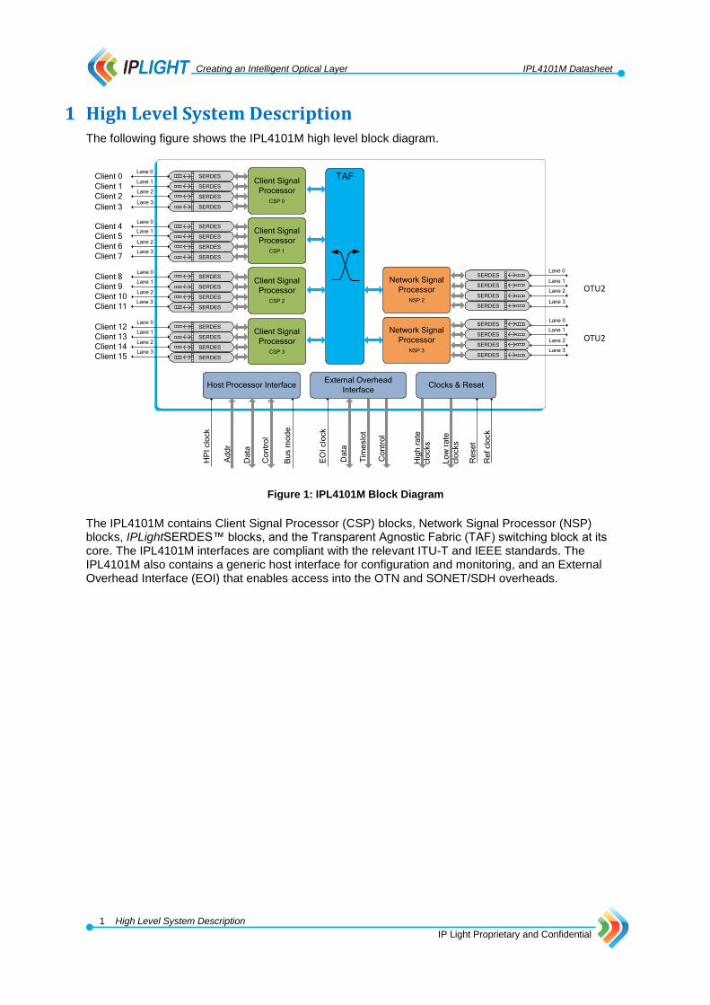
1 High Level System Description The following figure shows the IPL4101M high level block diagram.
TAFClient Signal
Processor
CSP 0
Client Signal
Processor
CSP 1
Client Signal
Processor
CSP 2
Client Signal
Processor
CSP 3
Client 13
Client 14
Client 15
Lane 0
Lane 1
Lane 2
Lane 3
Client 1
Client 2
Client 3
Client 4
Client 5
Client 6
Client 7
Client 8
Client 9
Client 10
Client 11
Client 12
Lane 0
Lane 1
Lane 2
Lane 3
Lane 0
Lane 1
Lane 2
Lane 3
Lane 0
Lane 1
Lane 2
Lane 3
Co
ntr
ol
Ad
dr
Bu
s m
od
e
Host Processor Interface
HP
I clo
ck
EO
I clo
ck
Tim
eslo
t
Co
ntr
ol
External Overhead
Interface
Re
f clo
ck
Hig
h r
ate
clo
cks
Re
se
t
Lo
w r
ate
clo
cks
Clocks & Reset
Da
ta
Da
ta
SERDES
SERDES
SERDES
SERDES
SERDES
SERDES
SERDES
SERDES
SERDES
SERDES
SERDES
SERDES
SERDES
SERDES
SERDES
SERDES
Client 0
Network Signal
Processor
NSP 2
OTU2
SERDES
SERDES
SERDES
SERDES
Lane 0
Lane 1
Lane 2
Lane 3
Network Signal
Processor
NSP 3
OTU2
SERDES
SERDES
SERDES
SERDES
Lane 0
Lane 1
Lane 2
Lane 3
Figure 1: IPL4101M Block Diagram
The IPL4101M contains Client Signal Processor (CSP) blocks, Network Signal Processor (NSP) blocks, IPLightSERDES™ blocks, and the Transparent Agnostic Fabric (TAF) switching block at its core. The IPL4101M interfaces are compliant with the relevant ITU-T and IEEE standards. The IPL4101M also contains a generic host interface for configuration and monitoring, and an External Overhead Interface (EOI) that enables access into the OTN and SONET/SDH overheads.

Creating an Intelligent Optical Layer IPL4101M Datasheet
2 High Level System Description
IP Light Proprietary and Confidential
The following figure shows the CSP block details.
Client Signal Processor
TAF
High Rate
Se
ria
l o
r X
AU
I o
r X
BI2
16
b/6
4b
co
nve
rsio
n
OC-192/STM-64/CBR10G
OTU2/2e/2f/1e/1f
ODU2/2e/2f/1e/1f
FC-1200 (GFP-T)
10GE(transparent)
10GEGFP-F 6.2/7.3
FC-1200(transparent)
Se
lecto
r
Se
lecto
r
La
ne
3
Se
lecto
r
Se
lecto
r
Se
lecto
r
GbE (GFP-T)
OC-48/STM-16/CBR2.5G
OTU1
FC-100
GbE (GFP-F)
OTU0
Se
lecto
r
Se
lecto
r
GbE (GFP-T)
OC-48/STM-16/CBR2.5G
OTU1
FC-100
GbE (GFP-F)
OTU0
Se
lecto
r
Se
lecto
r
GbE (GFP-T)
OC-48/STM-16/CBR2.5G
OTU1
FC-100
GbE (GFP-F)
OTU0
SERDES
Se
lecto
r
Se
lecto
r
GbE (GFP-T)
OC-48/STM-16/CBR2.5G
OTU1
FC-100
GbE (GFP-F)
OTU0
La
ne
0
SERDES
La
ne
1
SERDES
La
ne
2
SERDES
Figure 2: Client Signal Processor Detailed Block
The CSP supports a variety of signal types, including OTN client signals, which can be mapped into OTN carrier signals. The CSP features four parallel paths to operate on up to four low-rate signals and a separate path, which processes high-rate signals.
Within the High Rate signal block the following interfaces are supported:
Serial, lane 2 only, is relevant for all signal types
XAUI, lanes 0-3, is relevant only for FC-1200/10GE signal types
XBI2, lanes 1-2 (XBI2-2), lanes 0-3 (XBI2-4), is relevant only for OTU2/ODU2 signal types
Creating an Intelligent Optical Layer IPL4101M Datasheet
3 High Level System Description
IP Light Proprietary and Confidential
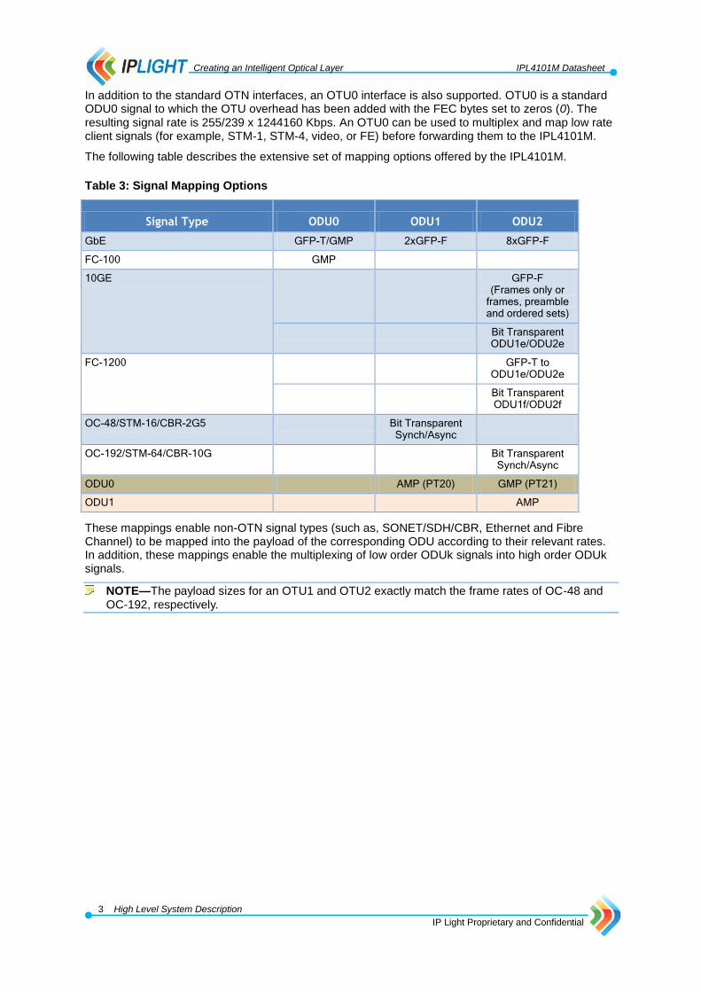
In addition to the standard OTN interfaces, an OTU0 interface is also supported. OTU0 is a standard ODU0 signal to which the OTU overhead has been added with the FEC bytes set to zeros (0). The resulting signal rate is 255/239 x 1244160 Kbps. An OTU0 can be used to multiplex and map low rate client signals (for example, STM-1, STM-4, video, or FE) before forwarding them to the IPL4101M.
The following table describes the extensive set of mapping options offered by the IPL4101M.
Table 3: Signal Mapping Options
Signal Type ODU0 ODU1 ODU2
GbE GFP-T/GMP 2xGFP-F 8xGFP-F
FC-100 GMP
10GE GFP-F (Frames only or
frames, preamble and ordered sets)
Bit Transparent ODU1e/ODU2e
FC-1200 GFP-T to ODU1e/ODU2e
Bit Transparent ODU1f/ODU2f
OC-48/STM-16/CBR-2G5 Bit Transparent Synch/Async
OC-192/STM-64/CBR-10G Bit Transparent Synch/Async
ODU0 AMP (PT20) GMP (PT21)
ODU1 AMP
These mappings enable non-OTN signal types (such as, SONET/SDH/CBR, Ethernet and Fibre Channel) to be mapped into the payload of the corresponding ODU according to their relevant rates. In addition, these mappings enable the multiplexing of low order ODUk signals into high order ODUk signals.
NOTE—The payload sizes for an OTU1 and OTU2 exactly match the frame rates of OC-48 and OC-192, respectively.
Creating an Intelligent Optical Layer IPL4101M Datasheet
4 High Level System Description
IP Light Proprietary and Confidential
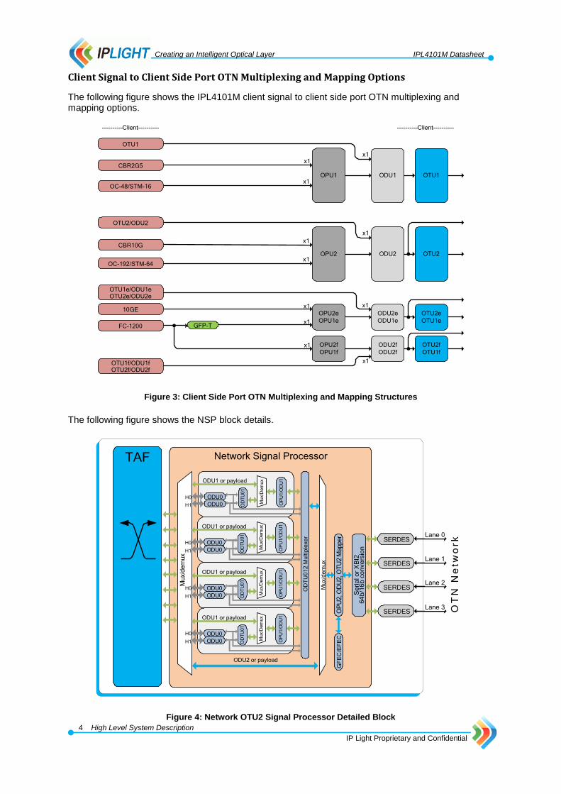
Client Signal to Client Side Port OTN Multiplexing and Mapping Options
The following figure shows the IPL4101M client signal to client side port OTN multiplexing and mapping options.
----------Client---------- ----------Client----------
CBR2G5
OC-48/STM-16
10GE
FC-1200
OC-192/STM-64
CBR10G
x1
x1
x1
x1
x1
x1
x1
OPU1 ODU1 OTU1
OPU2 ODU2 OTU2
OPU2e
OPU1e
ODU2e
ODU1e
OTU2e
OTU1e
OPU2f
OPU1f
ODU2f
ODU2f
OTU2f
OTU1f
GFP-T
OTU1f/ODU1fOTU2f/ODU2f
x1
OTU1e/ODU1eOTU2e/ODU2e
x1
OTU2/ODU2
x1
OTU1
x1
Figure 3: Client Side Port OTN Multiplexing and Mapping Structures
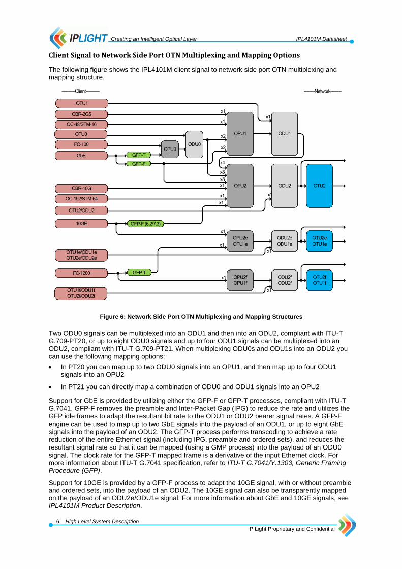
The following figure shows the NSP block details.
TAF Network Signal Processor
Mu
x/d
em
ux
OD
TU
01
2 M
ultip
lexe
r
Mu
x/d
em
ux
OP
U2, O
DU
2, O
TU
2 M
apper
GF
EC
/EF
EC
ODU2 or payload
H0
H1
H0
H1
H0
H1
H0
H1
Mux/
Dem
ux
ODU0
ODU0
OP
U1/O
DU
1
OD
TU
01
ODU1 or payload
Mux/
Dem
ux
ODU0
ODU0
OP
U1/O
DU
1
OD
TU
01
ODU1 or payload
Mux/
Dem
ux
ODU0
ODU0
OP
U1/O
DU
1
OD
TU
01
ODU1 or payload
Mux/
Dem
ux
ODU0
ODU0
OP
U1/O
DU
1
OD
TU
01
ODU1 or payload
Se
ria
l o
r X
BI2
64
b/1
6b
co
nve
rsio
n
OT
N N
etw
orkLane 0
SERDES
Lane 1SERDES
Lane 2SERDES
Lane 3SERDES
Figure 4: Network OTU2 Signal Processor Detailed Block

Creating an Intelligent Optical Layer IPL4101M Datasheet
5 High Level System Description
IP Light Proprietary and Confidential
The NSP supports OTN signals and offers ODU0/1/2 granularity connections to the TAF. The OTN signals can be processed at the ODU0, ODU1, or ODU2 levels.
The ODU2 interface supports signals at the ODU2 rate and is used when interfacing the IPL4101M to an external device, for example a device handling a higher order signal (ODU3 or ODU4), an external FEC, or an interface to a external switch matrix. The ODU2 signal is scrambled to allow clock recovery and includes the OPU2 signal (overhead and payload) and the ODU2 overhead.
NOTE—The ODU2 signal does not include the FEC. In addition, the OTU overhead fields are set to zero at the transmitter and ignored at the receiver, except for the FAS and MFAS, which are set at the transmitter and used at the receiver to synchronize with the ODU2 signal.
The MFAS signal is synchronized with the transmitted ODU2 frame. This synchronized signal is provided to help the higher order device to synchronize.
An ALM input signal can be activated by the external device to indicate the detection of a higher order alarm that requires consequent actions at the ODU2 level.
The following figure shows an example of an add/drop application involving two network side OTU2s and dropping a combination of SONET/SDH/CBR, Ethernet, and OTN client signals.
TAF
OP
U2
OD
U2
OT
U2
OP
U2
OD
U2
OT
U2
OTU2
OP
U1
OD
U1
OT
U1
ST
M-1
6
OTU2
OT
U1
OC
-48
CB
R2
G5
OD
U1
OD
U1
OD
U1
OP
U1
OP
U1
OD
U0
OP
U0
Gb
E
OD
U0
OP
U0
1G
FC
West East
ODU0 ODU0
ODU1ODU1
ODU1ODU1
ODU1ODU1
ODU0 ODU0
Figure 5: OTU2 Add/Drop Example
The West side OTU2 enters the device and is demultiplexed into ODU1 and ODU0 signals. One ODU1 signal and one ODU0 signal are passed through the TAF to the EAST side OTU2 output. Two ODU1 signals and one ODU0 signal from the West side OTU2 and two ODU1 signals and one ODU0 signal from the East side OTU2 are used for add/drop.
Creating an Intelligent Optical Layer IPL4101M Datasheet
6 High Level System Description
IP Light Proprietary and Confidential
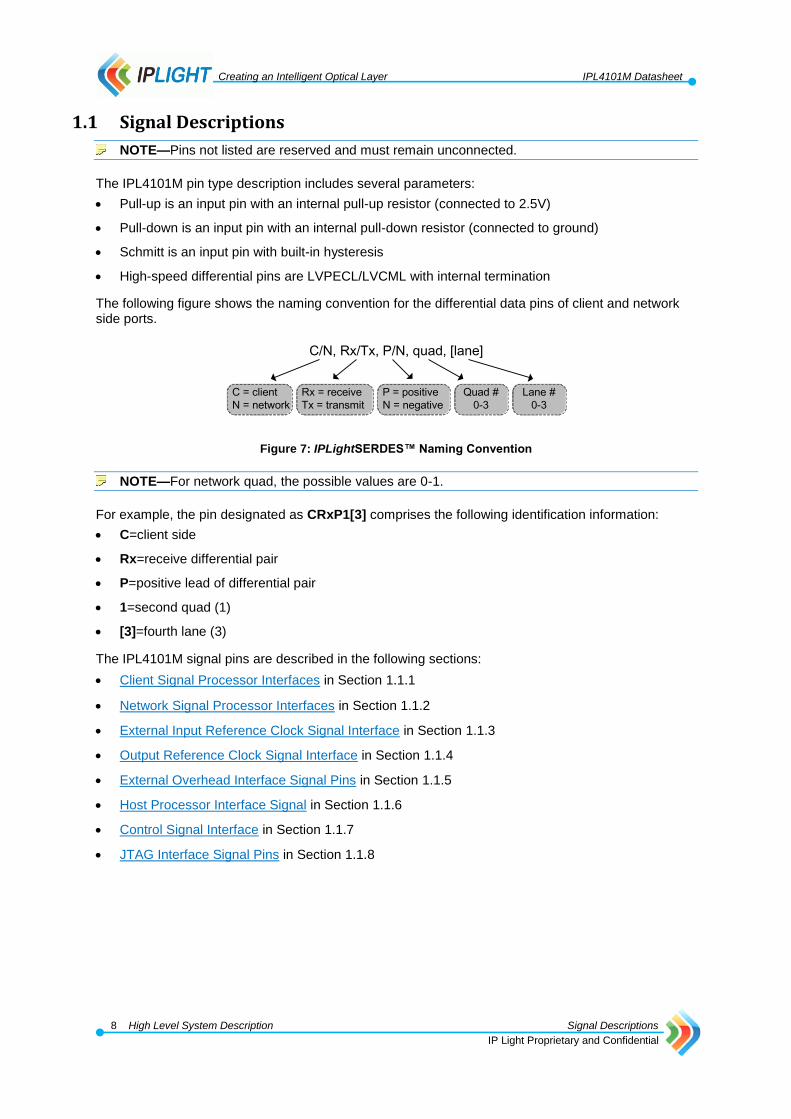
Client Signal to Network Side Port OTN Multiplexing and Mapping Options
The following figure shows the IPL4101M client signal to network side port OTN multiplexing and mapping structure.
CBR-2G5
OC-48/STM-16
10GE
FC-1200
OC-192/STM-64
CBR-10G
GFP-F (6.2/7.3)
x1
x1
x8
x1
x1
x1
x1
x1
x1
OPU1 ODU1
OPU2 ODU2 OTU2
OPU2e
OPU1e
ODU2e
ODU1e
OTU2e
OTU1e
OPU2f
OPU1f
ODU2f
ODU2f
OTU2f
OTU1f
x4
OPU0ODU0
x2
GFP-T
----------Client---------- --------Network--------
GbE
GFP-F
x2
GFP-T
x8
FC-100
OTU0
OTU1e/ODU1e
OTU2e/ODU2e
x1
OTU2/ODU2
x1
OTU1f/ODU1f
OTU2f/ODU2f
x1
OTU1
x1
Figure 6: Network Side Port OTN Multiplexing and Mapping Structures
Two ODU0 signals can be multiplexed into an ODU1 and then into an ODU2, compliant with ITU-T G.709-PT20, or up to eight ODU0 signals and up to four ODU1 signals can be multiplexed into an ODU2, compliant with ITU-T G.709-PT21. When multiplexing ODU0s and ODU1s into an ODU2 you can use the following mapping options:
In PT20 you can map up to two ODU0 signals into an OPU1, and then map up to four ODU1 signals into an OPU2
In PT21 you can directly map a combination of ODU0 and ODU1 signals into an OPU2
Support for GbE is provided by utilizing either the GFP-F or GFP-T processes, compliant with ITU-T G.7041. GFP-F removes the preamble and Inter-Packet Gap (IPG) to reduce the rate and utilizes the GFP idle frames to adapt the resultant bit rate to the ODU1 or ODU2 bearer signal rates. A GFP-F engine can be used to map up to two GbE signals into the payload of an ODU1, or up to eight GbE signals into the payload of an ODU2. The GFP-T process performs transcoding to achieve a rate reduction of the entire Ethernet signal (including IPG, preamble and ordered sets), and reduces the resultant signal rate so that it can be mapped (using a GMP process) into the payload of an ODU0 signal. The clock rate for the GFP-T mapped frame is a derivative of the input Ethernet clock. For more information about ITU-T G.7041 specification, refer to ITU-T G.7041/Y.1303, Generic Framing Procedure (GFP).
Support for 10GE is provided by a GFP-F process to adapt the 10GE signal, with or without preamble and ordered sets, into the payload of an ODU2. The 10GE signal can also be transparently mapped on the payload of an ODU2e/ODU1e signal. For more information about GbE and 10GE signals, see IPL4101M Product Description.

Creating an Intelligent Optical Layer IPL4101M Datasheet
7 High Level System Description
IP Light Proprietary and Confidential
Fibre Channel FC-100 and FC-1200 signals are supported. FC-100 (1.0625Gbps) is mapped using GMP into the payload of an ODU0 signal. FC-1200 is rate adapted by utilizing a GFP-T transcoding function and is then mapped into the payload of an ODU1e or ODU2e signal. The FC-1200 signal can also be transparently mapped to the payload of an ODU2f/ODU1f. For more information about FC-100 and FC-1200 signals, see IPL4101M Product Description.
NOTE—OTU2f and OTU1f are non-standard rates. The IPL4101M supports all the standard
(ITU-T G.709) rates plus several rates that are non-standard, but used in the industry.
SONET, SDH and CBR signals can be mapped into an OTU signal, asynchronously or synchronously.
The basic data flows of the IPL4101M are as follows:
Client port to network port data flow:
1. Traffic enters the device through one of the client ports. The data is then passed through and processed, as follows:
Monitored for alarms and degradations Mapped into an appropriate OTN payload
2. Data passes through the TAF and is mapped into the required OTN container.
If required, the data is also multiplexed at this point in the flow.
3. Data is forwarded to the network ports for transmission to the OTN network.
Network port to client port data flow:
1. Traffic enters from one of the network ports and is monitored for alarms and degradations.
If required, the data is demapped or demultiplexed at this point in the flow.
2. Data passes through the TAF. 3. Data is converted into the desired output signal type. 4. Data is sent out from one of the client ports.
The TAF switching capability also enables connections between network to network or client to client ports.
NOTE—Client to client connections are allowed, provided the following requirements are met: At least one of the ports is OTN The non-OTN port is not GFP-F mapped
The IPL4101M supports multicasting through the TAF, which enables configurations, such as, ODU0 based protected ring topologies. For example, a 1+1 protection scheme can be achieved by multicasting the transmit signal to both East and West (network) sides, while presenting the receive side the highest quality signal out of those received from both network ports.
The IPL4101M provides multiple Performance Monitoring (PM) options, available for all network or client signals, including advanced Tandem Connection Monitoring (TCM), PM counters, alarms and indications.
The IPL4101M contains functions that support network level maintenance. It offers both loopbacks and pseudo-random binary test sequences for every interface on the device, as well as, several other maintenance functions for specific interfaces. For more information about the available maintenance
functions, see IPLightSERDES™ Maintenance in Section 2.1.1.3.
IPL4101M system details are described in the following sections:
Signal Descriptions in Section 1.1
Power and Ground Pins in Section 1.2
Pinout By Quadrant in Section 1.3
Creating an Intelligent Optical Layer IPL4101M Datasheet
8 High Level System Description Signal Descriptions
IP Light Proprietary and Confidential
1.1 Signal Descriptions
NOTE—Pins not listed are reserved and must remain unconnected.
The IPL4101M pin type description includes several parameters:
Pull-up is an input pin with an internal pull-up resistor (connected to 2.5V)
Pull-down is an input pin with an internal pull-down resistor (connected to ground)
Schmitt is an input pin with built-in hysteresis
High-speed differential pins are LVPECL/LVCML with internal termination
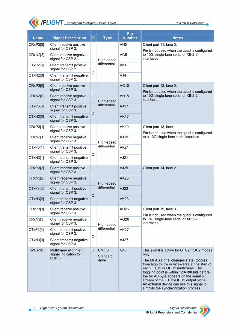
The following figure shows the naming convention for the differential data pins of client and network side ports.
C/N, Rx/Tx, P/N, quad, [lane]
P = positive
N = negative
C = client
N = network
Rx = receive
Tx = transmit
Quad #
0-3
Lane #
0-3
Figure 7: IPLightSERDES™ Naming Convention
NOTE—For network quad, the possible values are 0-1.
For example, the pin designated as CRxP1[3] comprises the following identification information:
C=client side
Rx=receive differential pair
P=positive lead of differential pair
1=second quad (1)
[3]=fourth lane (3)
The IPL4101M signal pins are described in the following sections:
Client Signal Processor Interfaces in Section 1.1.1
Network Signal Processor Interfaces in Section 1.1.2
External Input Reference Clock Signal Interface in Section 1.1.3
Output Reference Clock Signal Interface in Section 1.1.4
External Overhead Interface Signal Pins in Section 1.1.5
Host Processor Interface Signal in Section 1.1.6
Control Signal Interface in Section 1.1.7
JTAG Interface Signal Pins in Section 1.1.8

Creating an Intelligent Optical Layer IPL4101M Datasheet
9 High Level System Description Signal Descriptions
IP Light Proprietary and Confidential
1.1.1 Client Signal Processor Interfaces
The following table describes the pin locations and functions for the client signal ports.
Table 4: Client Side Signal Interface Pins
Name Signal Description IO Type Pin
Number Notes
CRxP0[0] Client receive positive signal for CSP 0.
I
High-speed differential
D18 Client port 0, lane 0.
Pin is not used when the quad is configured to 10G single-lane serial or XBI2-2 interfaces.
CRxN0[0] Client receive negative signal for CSP 0.
C18
CTxP0[0] Client transmit positive signal for CSP 0.
O
B17
CTxN0[0] Client transmit negative signal for CSP 0.
A17
CRxP0[1] Client receive positive signal for CSP 0.
I
High-speed differential
A19 Client port 1, lane 1.
Pin is not used when the quad is configured to a 10G single-lane serial interface. CRxN0[1] Client receive negative
signal for CSP 0. B19
CTxP0[1] Client transmit positive signal for CSP 0.
O
A21
CTxN0[1] Client transmit negative signal for CSP 0.
B21
CRxP0[2] Client receive positive signal for CSP 0.
I
High-speed differential
B25 Client port 2, lane 2.
CRxN0[2] Client receive negative signal for CSP 0.
A25
CTxP0[2] Client transmit positive signal for CSP 0.
O
B23
CTxN0[2] Client transmit negative signal for CSP 0.
A23
CRxP0[3] Client receive positive signal for CSP 0.
I
High-speed differential
C26 Client port 3, lane 3.
Pin is not used when the quad is configured to 10G single-lane serial or XBI2-2 interfaces.
CRxN0[3] Client receive negative signal for CSP 0.
D26
CTxP0[3] Client transmit positive signal for CSP 0.
O
A27
CTxN0[3] Client transmit negative signal for CSP 0.
B27
CRxP1[0] Client receive positive signal for CSP 1.
I
High-speed differential
D13 Client port 4, lane 0.
Pin is not used when the quad is configured to 10G single-lane serial or XBI2-2 interfaces.
CRxN1[0] Client receive negative signal for CSP 1.
C13
CTxP1[0] Client transmit positive signal for CSP 1.
O
B14
CTxN1[0] Client transmit negative signal for CSP 1.
A14

Creating an Intelligent Optical Layer IPL4101M Datasheet
10 High Level System Description Signal Descriptions
IP Light Proprietary and Confidential
Name Signal Description IO Type Pin
Number Notes
CRxP1[1] Client receive positive signal for CSP 1.
I
High-speed differential
A12 Client port 5, lane 1.
Pin is not used when the quad is configured to a 10G single-lane serial interface. CRxN1[1] Client receive negative
signal for CSP 1. B12
CTxP1[1] Client transmit positive signal for CSP 1.
O
A10
CTxN1[1] Client transmit negative signal for CSP 1.
B10
CRxP1[2] Client receive positive signal for CSP 1.
I
High-speed differential
B6 Client port 6, lane 2.
CRxN1[2] Client receive negative signal for CSP 1.
A6
CTxP1[2] Client transmit positive signal for CSP 1.
O
B8
CTxN1[2] Client transmit negative signal for CSP 1.
A8
CRxP1[3] Client receive positive signal for CSP 1.
I
High-speed differential
C5 Client port 7, lane 3.
Pin is not used when the quad is configured to 10G single-lane serial or XBI2-2 interfaces.
CRxN1[3] Client receive negative signal for CSP 1.
D5
CTxP1[3] Client transmit positive signal for CSP 1.
O
A4
CTxN1[3] Client transmit negative signal for CSP 1.
B4
CRxP2[0] Client receive positive signal for CSP 2.
I
High-speed differential
AG13 Client port 8, lane 0.
Pin is not used when the quad is configured to 10G single-lane serial or XBI2-2 interfaces.
CRxN2[0] Client receive negative signal for CSP 2.
AH13
CTxP2[0] Client transmit positive signal for CSP 2.
O
AJ14
CTxN2[0] Client transmit negative signal for CSP 2.
AK14
CRxP2[1] Client receive positive signal for CSP 2.
I
High-speed differential
AK12 Client port 9, lane 1.
Pin is not used when the quad is configured to a 10G single-lane serial interface. CRxN2[1] Client receive negative
signal for CSP 2. AJ12
CTxP2[1] Client transmit positive signal for CSP 2.
O
AK10
CTxN2[1] Client transmit negative signal for CSP 2.
AJ10
CRxP2[2] Client receive positive signal for CSP 2.
I
High-speed differential
AJ6 Client port 10, lane 2.
CRxN2[2] Client receive negative signal for CSP 2.
AK6
CTxP2[2] Client transmit positive signal for CSP 2.
O
AJ8
CTxN2[2] Client transmit negative signal for CSP 2.
AK8
Creating an Intelligent Optical Layer IPL4101M Datasheet
11 High Level System Description Signal Descriptions
IP Light Proprietary and Confidential
Name Signal Description IO Type Pin
Number Notes
CRxP2[3] Client receive positive signal for CSP 2.
I
High-speed differential
AH5 Client port 11, lane 3.
Pin is not used when the quad is configured to 10G single-lane serial or XBI2-2 interfaces.
CRxN2[3] Client receive negative signal for CSP 2.
AG5
CTxP2[3] Client transmit positive signal for CSP 2.
O
AK4
CTxN2[3] Client transmit negative signal for CSP 2.
AJ4
CRxP3[0] Client receive positive signal for CSP 3.
I
High-speed differential
AG18 Client port 12, lane 0.
Pin is not used when the quad is configured to 10G single-lane serial or XBI2-2 interfaces.
CRxN3[0] Client receive negative signal for CSP 3.
AH18
CTxP3[0] Client transmit positive signal for CSP 3.
O
AJ17
CTxN3[0] Client transmit negative signal for CSP 3.
AK17
CRxP3[1] Client receive positive signal for CSP 3.
I
High-speed differential
AK19 Client port 13, lane 1.
Pin is not used when the quad is configured to a 10G single-lane serial interface. CRxN3[1] Client receive negative
signal for CSP 3. AJ19
CTxP3[1] Client transmit positive signal for CSP 3.
O
AK21
CTxN3[1] Client transmit negative signal for CSP 3.
AJ21
CRxP3[2] Client receive positive signal for CSP 3.
I
High-speed differential
AJ25 Client port 14, lane 2.
CRxN3[2] Client receive negative signal for CSP 3.
AK25
CTxP3[2] Client transmit positive signal for CSP 3.
O
AJ23
CTxN3[2] Client transmit negative signal for CSP 3.
AK23
CRxP3[3] Client receive positive signal for CSP 3.
I
High-speed differential
AH26 Client port 15, lane 3.
Pin is not used when the quad is configured to 10G single-lane serial or XBI2-2 interfaces.
CRxN3[3] Client receive negative signal for CSP 3.
AG26
CTxP3[3] Client transmit positive signal for CSP 3.
O
AK27
CTxN3[3] Client transmit negative signal for CSP 3.
AJ27
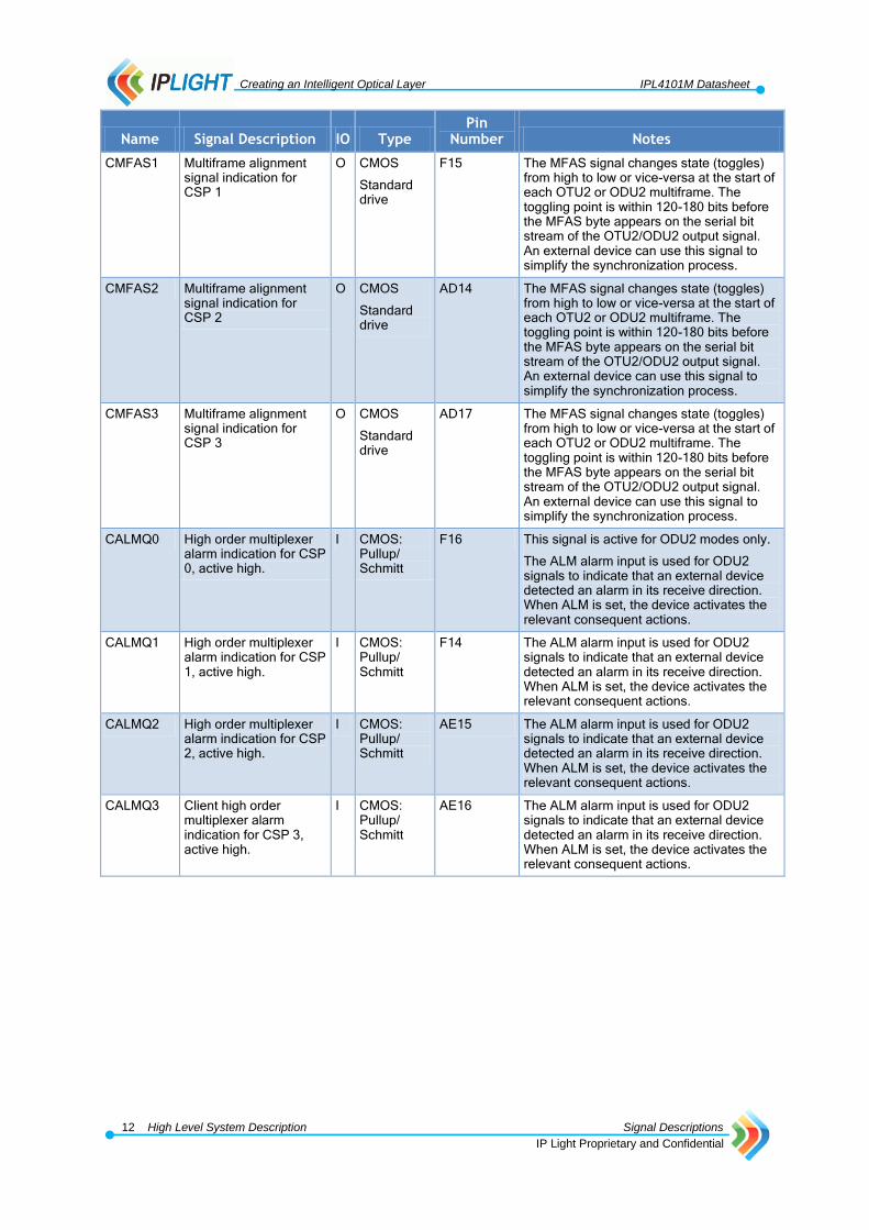
CMFAS0 Multiframe alignment signal indication for CSP 0
O CMOS
Standard drive
G17 This signal is active for OTU2/ODU2 modes only.
The MFAS signal changes state (toggles) from high to low or vice-versa at the start of each OTU2 or ODU2 multiframe. The toggling point is within 120-180 bits before the MFAS byte appears on the serial bit stream of the OTU2/ODU2 output signal. An external device can use this signal to simplify the synchronization process.
Creating an Intelligent Optical Layer IPL4101M Datasheet
12 High Level System Description Signal Descriptions
IP Light Proprietary and Confidential
Name Signal Description IO Type Pin
Number Notes
CMFAS1 Multiframe alignment signal indication for CSP 1
O CMOS
Standard drive
F15 The MFAS signal changes state (toggles) from high to low or vice-versa at the start of each OTU2 or ODU2 multiframe. The toggling point is within 120-180 bits before the MFAS byte appears on the serial bit stream of the OTU2/ODU2 output signal. An external device can use this signal to simplify the synchronization process.
CMFAS2 Multiframe alignment signal indication for CSP 2
O CMOS
Standard drive
AD14 The MFAS signal changes state (toggles) from high to low or vice-versa at the start of each OTU2 or ODU2 multiframe. The toggling point is within 120-180 bits before the MFAS byte appears on the serial bit stream of the OTU2/ODU2 output signal. An external device can use this signal to simplify the synchronization process.
CMFAS3 Multiframe alignment signal indication for CSP 3
O CMOS
Standard drive
AD17 The MFAS signal changes state (toggles) from high to low or vice-versa at the start of each OTU2 or ODU2 multiframe. The toggling point is within 120-180 bits before the MFAS byte appears on the serial bit stream of the OTU2/ODU2 output signal. An external device can use this signal to simplify the synchronization process.
CALMQ0 High order multiplexer alarm indication for CSP 0, active high.
I CMOS: Pullup/ Schmitt
F16 This signal is active for ODU2 modes only.
The ALM alarm input is used for ODU2 signals to indicate that an external device detected an alarm in its receive direction. When ALM is set, the device activates the relevant consequent actions.
CALMQ1 High order multiplexer alarm indication for CSP 1, active high.
I CMOS: Pullup/ Schmitt
F14 The ALM alarm input is used for ODU2 signals to indicate that an external device detected an alarm in its receive direction. When ALM is set, the device activates the relevant consequent actions.
CALMQ2 High order multiplexer alarm indication for CSP 2, active high.
I CMOS: Pullup/ Schmitt
AE15 The ALM alarm input is used for ODU2 signals to indicate that an external device detected an alarm in its receive direction. When ALM is set, the device activates the relevant consequent actions.
CALMQ3 Client high order multiplexer alarm indication for CSP 3, active high.
I CMOS: Pullup/ Schmitt
AE16 The ALM alarm input is used for ODU2 signals to indicate that an external device detected an alarm in its receive direction. When ALM is set, the device activates the relevant consequent actions.
Creating an Intelligent Optical Layer IPL4101M Datasheet
13 High Level System Description Signal Descriptions
IP Light Proprietary and Confidential
1.1.2 Network Signal Processor Interfaces
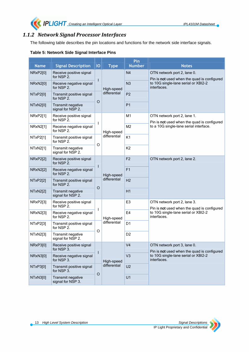
The following table describes the pin locations and functions for the network side interface signals.
Table 5: Network Side Signal Interface Pins
Name Signal Description IO Type Pin
Number Notes
NRxP2[0] Receive positive signal for NSP 2.
I
High-speed differential
N4 OTN network port 2, lane 0.
Pin is not used when the quad is configured to 10G single-lane serial or XBI2-2 interfaces.
NRxN2[0] Receive negative signal for NSP 2.
N3
NTxP2[0] Transmit positive signal for NSP 2.
O
P2
NTxN2[0] Transmit negative signal for NSP 2.
P1
NRxP2[1] Receive positive signal for NSP 2.
I
High-speed differential
M1 OTN network port 2, lane 1.
Pin is not used when the quad is configured to a 10G single-lane serial interface. NRxN2[1] Receive negative signal
for NSP 2. M2
NTxP2[1] Transmit positive signal for NSP 2.
O
K1
NTxN2[1] Transmit negative signal for NSP 2.
K2
NRxP2[2] Receive positive signal for NSP 2.
I
High-speed differential
F2 OTN network port 2, lane 2.
NRxN2[2] Receive negative signal for NSP 2.
F1
NTxP2[2] Transmit positive signal for NSP 2.
O
H2
NTxN2[2] Transmit negative signal for NSP 2.
H1
NRxP2[3] Receive positive signal for NSP 2.
I
High-speed differential
E3 OTN network port 2, lane 3.
Pin is not used when the quad is configured to 10G single-lane serial or XBI2-2 interfaces.
NRxN2[3] Receive negative signal for NSP 2.
E4
NTxP2[3] Transmit positive signal for NSP 2.
O
D1
NTxN2[3] Transmit negative signal for NSP 2.
D2
NRxP3[0] Receive positive signal for NSP 3.
I
High-speed differential
V4 OTN network port 3, lane 0.
Pin is not used when the quad is configured to 10G single-lane serial or XBI2-2 interfaces.
NRxN3[0] Receive negative signal for NSP 3.
V3
NTxP3[0] Transmit positive signal for NSP 3.
O
U2
NTxN3[0] Transmit negative signal for NSP 3.
U1
Creating an Intelligent Optical Layer IPL4101M Datasheet
14 High Level System Description Signal Descriptions
IP Light Proprietary and Confidential
Name Signal Description IO Type Pin
Number Notes
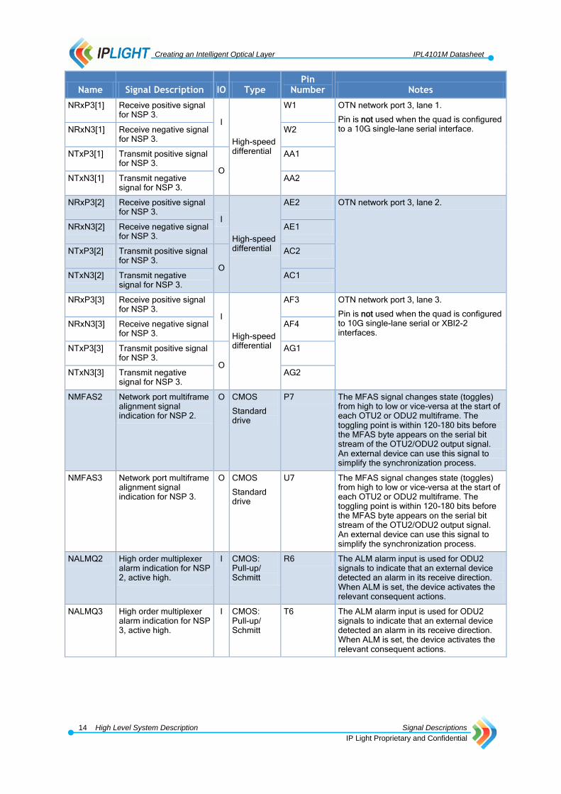
NRxP3[1] Receive positive signal for NSP 3.
I
High-speed differential
W1 OTN network port 3, lane 1.
Pin is not used when the quad is configured to a 10G single-lane serial interface. NRxN3[1] Receive negative signal
for NSP 3. W2
NTxP3[1] Transmit positive signal for NSP 3.
O
AA1
NTxN3[1] Transmit negative signal for NSP 3.
AA2
NRxP3[2] Receive positive signal for NSP 3.
I
High-speed differential
AE2 OTN network port 3, lane 2.
NRxN3[2] Receive negative signal for NSP 3.
AE1
NTxP3[2] Transmit positive signal for NSP 3.
O
AC2
NTxN3[2] Transmit negative signal for NSP 3.
AC1
NRxP3[3] Receive positive signal for NSP 3.
I
High-speed differential
AF3 OTN network port 3, lane 3.
Pin is not used when the quad is configured to 10G single-lane serial or XBI2-2 interfaces.
NRxN3[3] Receive negative signal for NSP 3.
AF4
NTxP3[3] Transmit positive signal for NSP 3.
O
AG1
NTxN3[3] Transmit negative signal for NSP 3.
AG2
NMFAS2 Network port multiframe alignment signal indication for NSP 2.
O CMOS
Standard drive
P7 The MFAS signal changes state (toggles) from high to low or vice-versa at the start of each OTU2 or ODU2 multiframe. The toggling point is within 120-180 bits before the MFAS byte appears on the serial bit stream of the OTU2/ODU2 output signal. An external device can use this signal to simplify the synchronization process.
NMFAS3 Network port multiframe alignment signal indication for NSP 3.
O CMOS
Standard drive
U7 The MFAS signal changes state (toggles) from high to low or vice-versa at the start of each OTU2 or ODU2 multiframe. The toggling point is within 120-180 bits before the MFAS byte appears on the serial bit stream of the OTU2/ODU2 output signal. An external device can use this signal to simplify the synchronization process.
NALMQ2 High order multiplexer alarm indication for NSP 2, active high.
I CMOS: Pull-up/ Schmitt
R6 The ALM alarm input is used for ODU2 signals to indicate that an external device detected an alarm in its receive direction. When ALM is set, the device activates the relevant consequent actions.
NALMQ3 High order multiplexer alarm indication for NSP 3, active high.
I CMOS: Pull-up/ Schmitt
T6 The ALM alarm input is used for ODU2 signals to indicate that an external device detected an alarm in its receive direction. When ALM is set, the device activates the relevant consequent actions.

Creating an Intelligent Optical Layer IPL4101M Datasheet
15 High Level System Description Signal Descriptions
IP Light Proprietary and Confidential
1.1.3 External Input Reference Clock Signal Interface Pins
The following table describes the pin locations and functions for the external input reference clock interface signals.
Table 6: External Input Reference Clock Signal Interface Pins
Name Description IO Type Pin
Number Notes
REFCLKP Reference clock positive signal.
I High-speed differential
F18 Oscillator frequency and accuracy: 155.52 MHz +/-20 ppm
REFCLKN Reference clock negative signal.
G18
1.1.4 Output Reference Clock Signal Interface Pins
The following table describes the pin locations and functions for the output reference clock interface signals.
Table 7: Output Reference Clock Signal Interface Pins
Name Description IO Type Pin
Number Notes
REC0P High-rate output reference clock positive signal.
O CMOS
High drive
AC22 After reset, these positive and negative signals are enabled, generating a clock signal by drawing on the external reference clock as its source. The high-rate output reference clock frequency is equal to the external reference clock frequency. Both positive and negative signal reference clocks represent the generated clock signal, but in opposite phases. To create a single differential signal, both positive and negative pins must be combined. You can disable and enable the high rate output reference clock, when disabled the clock output goes into Tri-state.
You can select the source of any of the output reference clocks to be:
Any recovered clock (of any signal carried by OTN containers)
Any transmit clock
External input reference clock
For more information about reference clocks and clock signals, see Reference Clock in Section 3.2 and Clock Parameters in Section 4.7.
REC0N High-rate output reference clock negative signal.
AB22

Creating an Intelligent Optical Layer IPL4101M Datasheet
16 High Level System Description Signal Descriptions
IP Light Proprietary and Confidential
Name Description IO Type Pin
Number Notes
REC1P High-rate output reference clock positive signal.
O CMOS
High drive
AD25 After reset, these positive and negative signals are disabled. Both positive and negative signal reference clocks represent the generated clock signal, but in opposite phases. To create a single differential signal, both positive and negative pins must be combined. You can enable and disable the high rate output reference clock, when disabled the clock output goes into Tri-state. You can select the source of any of the output reference clocks to be:
Any recovered clock (of any signal carried by OTN containers)
Any transmit clock
External input reference clock
For more information about reference clocks and clock signals, see Reference Clock in Section 3.2 and Clock Parameters in Section 4.7.
REC1N High-rate output reference clock negative signal.
AD24
REC2P High-rate output reference clock positive signal.
O CMOS
High drive
AE23 After reset, these positive and negative signals are disabled. Both positive and negative signal reference clocks represent the generated clock signal, but in opposite phases. To create a single differential signal, both positive and negative pins must be combined. You can enable and disable the high rate output reference clock, when disabled the clock output goes into Tri-state. You can select the source of any of the output reference clocks to be:
Any recovered clock (of any signal carried by OTN containers)
Any transmit clock
External input reference clock
For more information about reference clocks and clock signals, see Reference Clock in Section 3.2 and Clock Parameters in Section 4.7.
REC2N High-rate output reference clock negative signal.
AD23
REC3P High-rate output reference clock positive signal.
O CMOS
High drive
AE22 After reset, these positive and negative signals are disabled. Both positive and negative signal reference clocks represent the generated clock signal, but in opposite phases. To create a single differential signal, both positive and negative pins must be combined. You can enable and disable the high rate output reference clock, when disabled the clock output goes into Tri-state. You can select the source of any of the output reference clocks to be:
Any recovered clock (of any signal carried by OTN containers)
Any transmit clock
External input reference clock
For more information about reference clocks and clock signals, see Reference Clock in Section 3.2 and Clock Parameters in Section 4.7.
REC3N High-rate output reference clock negative signal.
AD22

Creating an Intelligent Optical Layer IPL4101M Datasheet
17 High Level System Description Signal Descriptions
IP Light Proprietary and Confidential
Name Description IO Type Pin
Number Notes
LRRC0 Low-rate output reference clock.
O CMOS
High drive
AE20 After reset, this low-rate reference output clock pin is enabled drawing on the external reference as its source. The low-rate reference clock frequency is equal to the external reference clock frequency divided by two. The low-rate reference clock is a single ended signal. You can disable and enable the low rate output reference clock, when disabled the clock output goes into Tri-state. You can select the source of any of the low-rate reference clocks to be:
Any recovered clock from any signal carried by OTN bearers
Any transmit clock of any IPL4101M interface
External input reference clock
For more information about reference clocks and clock signals, see Reference Clock in Section 3.2 and Clock Parameters in Section 4.7.
LRRC1 Low-rate output reference clock.
O CMOS
High drive
AD20 After reset, this low-rate reference output clock pin is disabled. The low-rate reference clock is a single ended signal. You can disable and enable the low rate output reference clock, when disabled the clock output goes into Tri-state. You can select the source of any of the low-rate reference clocks to be:
Any recovered clock from any signal carried by OTN bearers
Any transmit clock of any IPL4101M interface
External input reference clock
For more information about reference clocks and clock signals, see Reference Clock in Section 3.2 and Clock Parameters in Section 4.7.
LRRC2 Low-rate output clock. O CMOS
High drive
AC21 After reset, this low-rate reference output clock pin is disabled. The low-rate reference clock is a single ended signal. You can disable and enable the low rate output reference clock, when disabled the clock output goes into Tri-state. You can select the source of any of the low-rate reference clocks to be:
Any recovered clock from any signal carried by OTN bearers
Any transmit clock of any IPL4101M interface
External input reference clock
For more information about reference clocks and clock signals, see Reference Clock in Section 3.2 and Clock Parameters in Section 4.7.
Creating an Intelligent Optical Layer IPL4101M Datasheet
18 High Level System Description Signal Descriptions
IP Light Proprietary and Confidential
Name Description IO Type Pin
Number Notes
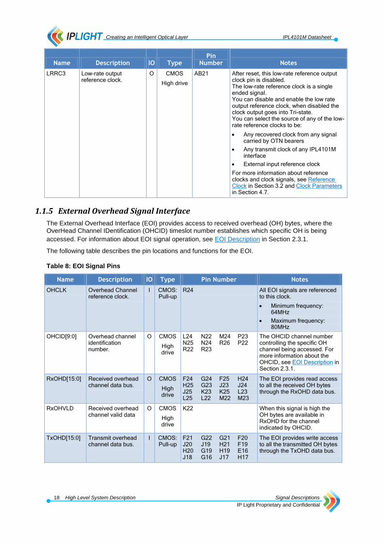
LRRC3 Low-rate output reference clock.
O CMOS
High drive
AB21 After reset, this low-rate reference output clock pin is disabled. The low-rate reference clock is a single ended signal. You can disable and enable the low rate output reference clock, when disabled the clock output goes into Tri-state. You can select the source of any of the low-rate reference clocks to be:
Any recovered clock from any signal carried by OTN bearers
Any transmit clock of any IPL4101M interface
External input reference clock
For more information about reference clocks and clock signals, see Reference Clock in Section 3.2 and Clock Parameters in Section 4.7.
1.1.5 External Overhead Signal Interface
The External Overhead Interface (EOI) provides access to received overhead (OH) bytes, where the OverHead Channel IDentification (OHCID) timeslot number establishes which specific OH is being
accessed. For information about EOI signal operation, see EOI Description in Section 2.3.1.
The following table describes the pin locations and functions for the EOI.
Table 8: EOI Signal Pins
Name Description IO Type Pin Number Notes
OHCLK Overhead Channel reference clock.
I CMOS: Pull-up
R24 All EOI signals are referenced to this clock.
Minimum frequency: 64MHz
Maximum frequency: 80MHz
OHCID[9:0] Overhead channel identification number.
O CMOS
High drive
L24 N22 M24 P23 N25 N24 R26 P22 R22 R23
The OHCID channel number controlling the specific OH channel being accessed. For more information about the OHCID, see EOI Description in Section 2.3.1.
RxOHD[15:0] Received overhead channel data bus.
O CMOS
High drive
F24 G24 F25 H24 H25 G23 J23 J24 J25 K23 K25 L23 L25 L22 M22 M23
The EOI provides read access to all the received OH bytes through the RxOHD data bus.
RxOHVLD Received overhead channel valid data
O CMOS
High drive
K22 When this signal is high the OH bytes are available in RxOHD for the channel indicated by OHCID.
TxOHD[15:0] Transmit overhead channel data bus.
I CMOS: Pull-up
F21 G22 G21 F20 J20 J19 H21 F19 H20 G19 H19 E16 J18 G16 J17 H17
The EOI provides write access to all the transmitted OH bytes through the TxOHD data bus.
Creating an Intelligent Optical Layer IPL4101M Datasheet
19 High Level System Description Signal Descriptions
IP Light Proprietary and Confidential
Name Description IO Type Pin Number Notes
TxOHRQ Transmit overhead channel data request.
O CMOS
High drive
J22 When this signal is high the OH bytes for the channel indicated by OHCID must be made available in TxOHD. The frame number can be derived from the TxOHMFAS signal.
TxOHMFAS Transmit overhead MFAS.
O CMOS
High drive
H22 A TxOHMFAS signal is provided for each overhead channel (according to the respective OHCID channel number). When TxOHMFAS is high it indicates the start of a new multiframe for the current channel. Accordingly, the TxOHMFAS signal associated with the particular channel remains high for the complete transaction for frame 0 and is low for the next 255 consecutive channel frames.
For more information about the EOI, see External Overhead Interface in Section 2.3.
1.1.6 Host Processor Interface Pins
The following table describes the pin locations and functions for the HPI.
Table 9: HPI Signal Pins
Name Description IO Type Pin
Number Notes
CCLK Host Processor timing input reference clock.
I CMOS AC15 All HPI signals are referenced to this clock. Minimum frequency: 33MHz Maximum frequency:
72MHz
FREE CPU operation mode selection.
I CMOS: Pull-up
and Schmitt
AC10 Select the CPU mode of operation between: Freescale: FREE=1 Intel: FREE=0
END Endian selection. I CMOS: Pull-up
and Schmitt
AD15 Valid for Intel mode only (FREE=0). Little endian: END=1 Big endian: END=0 For more information about endian modes, see HPI Intel Mode in Section 2.4.3.
LCS_ADS Chip Select or Address Status.
I CMOS: Pull-up
F13 Chip Select or Address Status mode depends on the selected CPU operation mode: Freescale mode (FREE=1):
Chip Select Intel mode (FREE=0):
Address Status
WE_R Write Enable or Read.
I CMOS J10 Write or Read Mode depends on the selected CPU operation mode: Freescale mode (FREE=1):
WE_R=1 Read WE_R=0 Write
Intel mode (FREE=0): WE_R=1 Write WE_R=0 Read

Creating an Intelligent Optical Layer IPL4101M Datasheet
20 High Level System Description Signal Descriptions
IP Light Proprietary and Confidential
Name Description IO Type Pin
Number Notes
LGTA Acknowledgment or Ready Receive assertion.
O CMOS
High drive
H14 Transaction complete indication depends on the selected CPU operation mode: Freescale mode (FREE=1):
LGTA assertion Intel mode (FREE=0):
Ready Receive assertion
D[31:0] Data bus. I/O
CMOS
High drive
G14 H15 J15 J14 G12 G13 H11 J13 J12 F10 H10 F9 G9 H9 F8 G8 G7 F6 G6 H7 J8 J7 H6 K6 K8 L6 M7 K7 K9 L9 N7 M6
AD[23:2] Address bus. I CMOS AB9 AA9 AC7 AC6 AB8 AB6 AA6 AB7 W9 V9 AA8 Y6 Y8 Y7 V7 W7 W8 V6 U9 T9 T8 U8
The lower two address bits (A0 and A1 in the microprocessor) are not connected and all addresses must be aligned to 32 bits, as the IPL4101M operates as a 32-bit peripheral.
OE Output enable. I CMOS AC14 Active low. Controls the data signal drivers. When active low the data signals are active.
IRQ_N Master interrupt request.
O CMOS: Tri-state /normal
High drive
J9 Active low. This pin has the following operational modes: Normal mode
Normal mode drives the signal as a regular output pin. High level (1) indicates that there is no interrupt. Low level (0) indicates that there is an active non-masked pending interrupt.
Tri-state mode Tri-state mode is a WIRED-OR connection that allows multiple sources to drive a single host processor pin. When there are no interrupts active, the output is High-Z. When a non-masked pending interrupt is active, the output drives a low level (0) signal. IRQ_N=0: outputs a 0 IRQ_N=1: output switches to high-Z
For more information about the host processor interface, see Host Processor Interface in Section 2.4.
Creating an Intelligent Optical Layer IPL4101M Datasheet
21 High Level System Description Signal Descriptions
IP Light Proprietary and Confidential
1.1.7 Control Signal Interface Pins
The following table describes the control signal interface pins.
Table 10: Control Signal Interface Pins
Name Description IO Type Pin
Number Notes
PMSYN Performance monitoring synchronization input.
I CMOS: Pull-up and
Schmitt
H12 When a performance monitoring counter is configured in Latching mode, changing (toggling) the state of this pin from high to low or low to high, it latches the contents of the counter into its respective shadow register. For more information about configuring options for the PM counters to use this signal, refer to the Apodis I User Manual.
RST_N Device reset. I CMOS: Pull-up and
Schmitt
G11 Active low. Activating the reset pin resets the whole device and sets all registers to their default values.
1.1.8 JTAG Interface Signal Pins
The following table describes the pin locations and functions for the JTAG interface signals.
Table 11: JTAG Interface Pins
Name Description IO Type Pin
Number Notes
TDI Test data input I CMOS: Pull-up V25
TDO Test data output O
CMOS: Tri-state
Standard drive
V24
TCK Test clock I CMOS: Pull-up AC25
TMS Test mode selection I CMOS: Pull-up AE25
TRST Test reset I CMOS: Pull-up and Schmidt
F11
For more information about the JTAG interface, see JTAG Interface in Section 2.5 and JTAG
Characteristics in Section 4.6.

Creating an Intelligent Optical Layer IPL4101M Datasheet
22 High Level System Description Power and Ground Pins
IP Light Proprietary and Confidential
1.2 Power and Ground Pins
The following table describes the power and ground pin locations.
Table 12: Power and Ground Pins
Name Description Type Pin Number Notes
VDD10 1.0V digital power supply.
Power K20 K18 K16 K12 K10 L21 L19 L17 L15 L13 L11 M20 M18 M16 M14 M12 N21 N19 N17 N15 N13 N11 P20 P18 P16 P14 P12 P10 R21 R19 R17 R15 R13 R11 T20 T18 T16 T14 T12 T10 U21 U19 U17 U15 U13 U11 V20 V18 V16 V14 V12 V10 W21 W19 W17 W15 W13 Y20 Y18 Y16 Y14 Y12 Y10 AA21 AA19 AA17 AA15 AA13 AA11
VDD10B 1.0V analog power supply, bottom side.
Power AF24 AF7 AG25 AG24 AG23 AG21 AG20 AG19 AG12 AG11 AG10 AG8 AG7 AG6
VDD10L 1.0V analog power supply, left side.
Power F4 G5 G4 H4 K4 L4 M4 W4 Y4 AA4 AC4 AD5 AD4 AE4
VDD10O General 1.0V analog power supply, general purpose.
Power A16 B15 D15 R29 R27 R4 R2 T30 T28 T26 T5 T3 T1 AG16 AH15 AJ16 AK15
VDD10PB 1.0V analog power supply, phase-locked loop bottom side.
Power AG22 AG9 AH22 AH9
VDD10PL 1.0V analog power supply, phase-locked loop left side.
Power J4 J3 AB4 AB3
VDD10PR 1.0V analog power supply, phase-locked loop right side.
Power J28 J27 AB28 AB27
VDD10PT 1.0V analog power supply, phase-locked loop top side.
Power C22 C9 D22 D9
VDD10R 1.0V analog power supply, right side.
Power F27 G27 G26 H27 K27 L27 M27 W27 Y27 AA27 AC27 AD27 AD26 AE27
VDD10T 1.0V analog power supply, top side.
Power D25 D24 D23 D21 D20 D19 D12 D11 D10 D8 D7 D6 E24 E7
VDD25 2.5V digital power supply.
Power F22 F12 G25 G15 H18 H8 J21 J11 K24 K14 L7 M10 N23 P6 R9 T22 U25 U6 V23 V8 Y24 AA7 AB20 AB17 AB10 AC23 AC13 AD16 AD6 AE19 AE17 AE9
VDD25B 2.5V analog power supply, bottom side.
Power AH25 AH24 AH23 AH21 AH20 AH19 AH12 AH11 AH10 AH8 AH7 AH6
VDD25L 2.5V analog power supply, left side.
Power F3 G3 H3 K3 L3 M3 W3 Y3 AA3 AC3 AD3 AE3

Creating an Intelligent Optical Layer IPL4101M Datasheet
23 High Level System Description Power and Ground Pins
IP Light Proprietary and Confidential
Name Description Type Pin Number Notes
VDD25R 2.5V analog power supply, right side.
Power F28 G28 H28 K28 L28 M28 W28 Y28 AA28 AC28 AD28 AE28
VDD25T 2.5V analog power supply, top side.
Power C25 C24 C23 C21 C20 C19 C12 C11 C10 C8 C7 C6
VSS Digital ground pins.
Ground A29 A2 B30 B29 B2 B1 F17 F7 G20 G10 H23 H13 J16 J6 K21 K17 K15 K11 L20 L18 L16 L14 L12 M25 M19 M17 M15 M13 M11 N20 N18 N16 N14 N12 N10 N8 P25 P21 P19 P17 P15 P13 P11 R20 R18 R16 R14 R12 R10 T23 T21 T19 T17 T15 T13 T11 T7 U22 U20 U18 U16 U14 U12 V22 V19 V17 V15 V13 V11 W23 W20 W18 W16 W14 W12 W11 W10 W6 Y21 Y19 Y17 Y15 Y13 Y11 Y9 AA22 AA20 AA16 AA14 AA10 AB25 AB15 AC24 AC20 AC18 AC16 AC8 AD21 AD19 AD11 AE24 AE14 AE12 AF15 AJ30 AJ29 AJ2 AJ1 AK29 AK2
VSSA Analog ground pins.
Ground A28 A26 A24 A22 A20 A18 A15 A13 A11 A9 A7 A5 A3 B28 B26 B24 B22 B20 B18 B16 B13 B11 B9 B7 B5 B3 C30 C29 C28 C27 C17 C15 C14 C4 C3 C2 C1 D28 D27 D17 D16 D14 D4 D3 E30 E29 E26 E25 E23 E22 E21 E20 E19 E18 E13 E12 E11 E10 E9 E8 E6 E5 E2 E1 F26 F5 G30 G29 G2 G1 H26 H5 J30 J29 J26 J5 J2 J1 K26 K19 K13 K5 L30 L29 L26 L10 L5 L2 L1 M26 M21 M5 N30 N29 N26 N5 N2 N1 P28 P27 P4 P3 R30 R28 R3 R1 T29 T27 T4 T2 U28 U27 U10 U4 U3 V30 V29 V26 V21 V5 V2 V1 W26 W5 Y30 Y29 Y26 Y5 Y2 Y1 AA26 AA18 AA12 AA5 AB30 AB29 AB26 AB5 AB2 AB1 AC26 AC5 AD30 AD29 AD2 AD1 AE26 AE5 AF30 AF29 AF26 AF25 AF23 AF22 AF21 AF20 AF19 AF18 AF16 AF13 AF12 AF11 AF10 AF9 AF8 AF6 AF5 AF2 AF1 AG28 AG27 AG17 AG15 AG14 AG4 AG3 AH30 AH29 AH28 AH27 AH17 AH16 AH14 AH4 AH3 AH2 AH1 AJ28 AJ26 AJ24 AJ22 AJ20 AJ18 AJ15 AJ13 AJ11 AJ9 AJ7 AJ5 AJ3 AK28 AK26 AK24 AK22 AK20 AK18 AK16 AK13 AK11 AK9 AK7 AK5 AK3

Creating an Intelligent Optical Layer IPL4101M Datasheet
24 High Level System Description Pinout
IP Light Proprietary and Confidential
1.3 Pinout
The following figure shows the IPL4101M pinout locations in the upper-left quadrant.
30 29 28 27 26 25 24 23 22 21 20 19 18 17 16
A VSS VSSA CTxP0[3] VSSA CRxN0[2] VSSA CTxN0[2] VSSA CTxP0[1] VSSA CRxP0[1] VSSA CTxN0[0] VDD10O
B VSS VSS VSSA CTxN0[3] VSSA CRxP0[2] VSSA CTxP0[2] VSSA CTxN0[1] VSSA CRxN0[1] VSSA CTxP0[0] VSSA
C VSSA VSSA VSSA VSSA CRxP0[3] VDD25T VDD25T VDD25T VDD10PT VDD25T VDD25T VDD25T CRxN0[0] VSSA VDD10O
D VSSA VSSA CRxN0[3] VDD10T VDD10T VDD10T VDD10PT VDD10T VDD10T VDD10T CRxP0[0] VSSA VSSA
E VSSA VSSA VSSA VSSA VDD10T VSSA VSSA VSSA VSSA VSSA VSSA TxOHD4
F VDD25R VDD10R VSSA RxOHD13RxOHD15 VDD25 TxOHD15 TxOHD12 TxOHD8 REFCLKP VSS CALMQ0
G VSSA VSSA VDD25R VDD10R VDD10R VDD25 RxOHD14RxOHD10 TxOHD14 TxOHD13 VSS TxOHD6 REFCLKN CMFAS0 TxOHD2
H VDD25R VDD10R VSSA RxOHD11RxOHD12 VSS TxOHMFASTxOHD9 TxOHD7 TxOHD5 VDD25 TxOHD0
J VSSA VSSA VDD10PRVDD10PR VSSA RxOHD7 RxOHD8 RxOHD9 TxOHRQ VDD25 TxOHD11 TxOHD10 TxOHD3 TxOHD1 VSS
K VDD25R VDD10R VSSA RxOHD5 VDD25 RxOHD6 RxOHVLD VSS VDD10 VSSA VDD10 VSS VDD10
L VSSA VSSA VDD25R VDD10R VSSA RxOHD3 OHCID9 RxOHD4 RxOHD2 VDD10 VSS VDD10 VSS VDD10 VSS
M VDD25R VDD10R VSSA VSS OHCID7 RxOHD0 RxOHD1 VSSA VDD10 VSS VDD10 VSS VDD10
N VSSA VSSA VSSA OHCID5 OHCID4 VDD25 OHCID8 VDD10 VSS VDD10 VSS VDD10 VSS
P VSSA VSSA VSS OHCID6 OHCID2 VSS VDD10 VSS VDD10 VSS VDD10
R VSSA VDD10O VSSA VDD10O OHCID3 OHCLK OHCID0 OHCID1 VDD10 VSS VDD10 VSS VDD10 VSS
Figure 8: IPL4101M Pinout Upper Left Quadrant (Bottom View)
Key
Signal pins:
Power pins:
Ground pins:
Reserved: Pins not indicated are reserved and must remain unconnected.

Creating an Intelligent Optical Layer IPL4101M Datasheet
25 High Level System Description Pinout
IP Light Proprietary and Confidential
The following figure shows the IPL4101M pinout locations in the upper-right quadrant.
15 14 13 12 11 10 9 8 7 6 5 4 3 2 1
VSSA CTxN1[0] VSSA CRxP1[1] VSSA CTxP1[1] VSSA CTxN1[2] VSSA CRxN1[2] VSSA CTxP1[3] VSSA VSS A
VDD10O CTxP1[0] VSSA CRxN1[1] VSSA CTxN1[1] VSSA CTxP1[2] VSSA CRxP1[2] VSSA CTxN1[3] VSSA VSS VSS B
VSSA VSSA CRxN1[0] VDD25T VDD25T VDD25T VDD10PT VDD25T VDD25T VDD25T CRxP1[3] VSSA VSSA VSSA VSSA C
VDD10O VSSA CRxP1[0] VDD10T VDD10T VDD10T VDD10PT VDD10T VDD10T VDD10T CRxN1[3] VSSA VSSA NTxN2[3]NTxP2[3] D
VSSA VSSA VSSA VSSA VSSA VSSA VDD10T VSSA VSSA NRxN2[3] NRxP2[3] VSSA VSSA E
CMFAS1 CALMQ1 LCS_ADS VDD25 TRST D[22] D[20] D[17] VSS D[14] VSSA VDD10L VDD25L NRxP2[2]NRxN2[2] F
VDD25 D[31] D[26] D[27] RST_N VSS D[19] D[16] D[15] D[13] VDD10L VDD10L VDD25L VSSA VSSA G
D[30] LGTA VSS PMSYN D[25] D[21] D[18] VDD25 D[12] D[9] VSSA VDD10L VDD25L NTxP2[2] NTxN2[2] H
D[29] D[28] D[24] D[23] VDD25 WE_R IRQ_N D[11] D[10] VSS VSSA VDD10PL VDD10PL VSSA VSSA J
VSS VDD25 VSSA VDD10 VSS VDD10 D[3] D[7] D[4] D[8] VSSA VDD10L VDD25L NTxN2[1]NTxP2[1] K
VDD10 VSS VDD10 VSS VDD10 VSSA D[2] VDD25 D[6] VSSA VDD10L VDD25L VSSA VSSA L
VSS VDD10 VSS VDD10 VSS VDD25 D[5] D[0] VSSA VDD10L VDD25L NRxN2[1] NRxP2[1] M
VDD10 VSS VDD10 VSS VDD10 VSS VSS D[1] VSSA NRxP2[0]NRxN2[0] VSSA VSSA N
VSS VDD10 VSS VDD10 VSS VDD10 NMFAS2 VDD25 VSSA VSSA NTxP2[0] NTxN2[0] P
VDD10 VSS VDD10 VSS VDD10 VSS VDD25 NALMQ2 VDD10O VSSA VDD10O VSSA R
Figure 9: IPL4101M Pinout Upper Right Quadrant (Bottom View)
Key
Signal pins:
Power pins:
Ground pins:
Reserved: Pins not indicated are reserved and must remain unconnected.
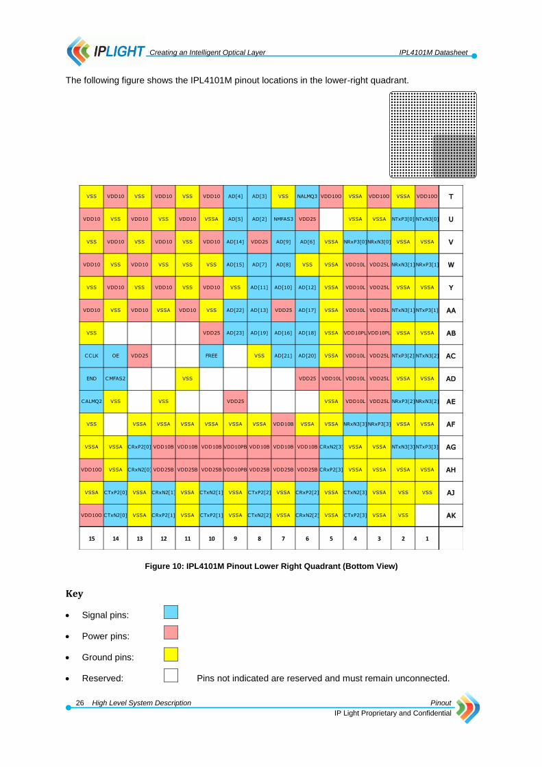
Creating an Intelligent Optical Layer IPL4101M Datasheet
26 High Level System Description Pinout
IP Light Proprietary and Confidential
The following figure shows the IPL4101M pinout locations in the lower-right quadrant.
VSS VDD10 VSS VDD10 VSS VDD10 AD[4] AD[3] VSS NALMQ3 VDD10O VSSA VDD10O VSSA VDD10O T
VDD10 VSS VDD10 VSS VDD10 VSSA AD[5] AD[2] NMFAS3 VDD25 VSSA VSSA NTxP3[0] NTxN3[0] U
VSS VDD10 VSS VDD10 VSS VDD10 AD[14] VDD25 AD[9] AD[6] VSSA NRxP3[0]NRxN3[0] VSSA VSSA V
VDD10 VSS VDD10 VSS VSS VSS AD[15] AD[7] AD[8] VSS VSSA VDD10L VDD25L NRxN3[1] NRxP3[1] W
VSS VDD10 VSS VDD10 VSS VDD10 VSS AD[11] AD[10] AD[12] VSSA VDD10L VDD25L VSSA VSSA Y
VDD10 VSS VDD10 VSSA VDD10 VSS AD[22] AD[13] VDD25 AD[17] VSSA VDD10L VDD25L NTxN3[1]NTxP3[1] AA
VSS VDD25 AD[23] AD[19] AD[16] AD[18] VSSA VDD10PL VDD10PL VSSA VSSA AB
CCLK OE VDD25 FREE VSS AD[21] AD[20] VSSA VDD10L VDD25L NTxP3[2] NTxN3[2] AC
END CMFAS2 VSS VDD25 VDD10L VDD10L VDD25L VSSA VSSA AD
CALMQ2 VSS VSS VDD25 VSSA VDD10L VDD25L NRxP3[2]NRxN3[2] AE
VSS VSSA VSSA VSSA VSSA VSSA VSSA VDD10B VSSA VSSA NRxN3[3] NRxP3[3] VSSA VSSA AF
VSSA VSSA CRxP2[0] VDD10B VDD10B VDD10B VDD10PB VDD10B VDD10B VDD10B CRxN2[3] VSSA VSSA NTxN3[3]NTxP3[3] AG
VDD10O VSSA CRxN2[0] VDD25B VDD25B VDD25B VDD10PB VDD25B VDD25B VDD25B CRxP2[3] VSSA VSSA VSSA VSSA AH
VSSA CTxP2[0] VSSA CRxN2[1] VSSA CTxN2[1] VSSA CTxP2[2] VSSA CRxP2[2] VSSA CTxN2[3] VSSA VSS VSS AJ
VDD10O CTxN2[0] VSSA CRxP2[1] VSSA CTxP2[1] VSSA CTxN2[2] VSSA CRxN2[2] VSSA CTxP2[3] VSSA VSS AK
15 14 13 12 11 10 9 8 7 6 5 4 3 2 1
Figure 10: IPL4101M Pinout Lower Right Quadrant (Bottom View)
Key
Signal pins:
Power pins:
Ground pins:
Reserved: Pins not indicated are reserved and must remain unconnected.

Creating an Intelligent Optical Layer IPL4101M Datasheet
27 High Level System Description Pinout
IP Light Proprietary and Confidential
The following figure shows the IPL4101M pinout locations in the lower-left quadrant.
T VDD10O VSSA VDD10O VSSA VDD10O VSS VDD25 VSS VDD10 VSS VDD10 VSS VDD10
U VSSA VSSA VDD25 VSS VDD10 VSS VDD10 VSS VDD10 VSS
V VSSA VSSA VSSA TDI TDO VDD25 VSS VSSA VDD10 VSS VDD10 VSS VDD10
W VDD25R VDD10R VSSA VSS VDD10 VSS VDD10 VSS VDD10 VSS
Y VSSA VSSA VDD25R VDD10R VSSA VDD25 VSS VDD10 VSS VDD10 VSS VDD10
AA VDD25R VDD10R VSSA VSS VDD10 VSS VDD10 VSSA VDD10 VSS
AB VSSA VSSA VDD10PRVDD10PR VSSA VSS REC0N LRRC3 VDD25 VDD25
AC VDD25R VDD10R VSSA TCK VSS VDD25 REC0P LRRC2 VSS VSS VSS
AD VSSA VSSA VDD25R VDD10R VDD10R REC1P REC1N REC2N REC3N VSS LRRC1 VSS CMFAS3 VDD25
AE VDD25R VDD10R VSSA TMS VSS REC2P REC3P LRRC0 VDD25 VDD25 CALMQ3
AF VSSA VSSA VSSA VSSA VDD10B VSSA VSSA VSSA VSSA VSSA VSSA VSSA
AG VSSA VSSA CRxN3[3] VDD10B VDD10B VDD10B VDD10PB VDD10B VDD10B VDD10B CRxP3[0] VSSA VDD10O
AH VSSA VSSA VSSA VSSA CRxP3[3] VDD25B VDD25B VDD25B VDD10PB VDD25B VDD25B VDD25B CRxN3[0] VSSA VSSA
AJ VSS VSS VSSA CTxN3[3] VSSA CRxP3[2] VSSA CTxP3[2] VSSA CTxN3[1] VSSA CRxN3[1] VSSA CTxP3[0] VDD10O
AK VSS VSSA CTxP3[3] VSSA CRxN3[2] VSSA CTxN3[2] VSSA CTxP3[1] VSSA CRxP3[1] VSSA CTxN3[0] VSSA
30 29 28 27 26 25 24 23 22 21 20 19 18 17 16
Figure 11: IPL4101M Pinout Lower Left Quadrant (Bottom View)
Key
Signal pins:
Power pins:
Ground pins:
Reserved: Pins not indicated are reserved and must remain unconnected.
Creating an Intelligent Optical Layer IPL4101M Datasheet
28 Functional Description
IP Light Proprietary and Confidential
2 Functional Description Functional characteristics and features of the IPL4101M are described in the following sections:
Client and Network Interfaces in Section 2.1
Clock Outputs in Section 2.2
External Overhead Interface in Section 2.3
Host Processor Interface in Section 2.4
JTAG Interface in Section 2.5
2.1 Client and Network Interfaces
Each client or network interface includes an IPLightSERDES™.
The interfaces may be configured as serial, XAUI or XBI2 interfaces.
Client and network interfaces are described in the following sections:
IPLightSERDES™ in Section 2.1.1
Serial Interface in Section 2.1.2
XBI2 Interface in Section 2.1.3
XAUI Interface in Section 2.1.4
FEC in Section 2.1.5
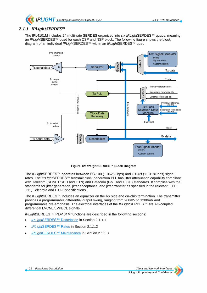
Creating an Intelligent Optical Layer IPL4101M Datasheet
29 Functional Description Client and Network Interfaces
IP Light Proprietary and Confidential
2.1.1 IPLightSERDES™
The IPL4101M includes 24 multi-rate SERDES organized into six IPLightSERDES™ quads, meaning an IPLightSERDES™ quad for each CSP and NSP block. The following figure shows the block diagram of an individual IPLightSERDES™ within an IPLightSERDES™ quad.
Tx PLL
Se
lect
Clock/Data Recovery
Serializer
DeserializerRX
TXTx data
Rx data
External reference clk
Tx serial data
Pre-emphasis
control
Tx output
swing
control
Rx serial data
Rx threshold
adjust
Lin
e lo
op
ba
ck
Rx clk
Tx clk
Test Signal Generator PRBS
Square wave
Custom pattern
Test Signal Monitor PRBS
Custom pattern
Se
lect
Se
lect
Se
lect
Primary reference clk
Secondary reference clk
Tx Clock Selection State
Machine
Control
Primary ReferenceAlarms
Secondary ReferenceAlarms
Te
rmin
al lo
op
ba
ck
Figure 12: IPLightSERDES™ Block Diagram
The IPLightSERDES™ operates between FC-100 (1.0625Gbps) and OTU2f (11.318Gbps) signal rates. The IPLightSERDES™ transmit clock generation PLL has jitter attenuation capability compliant with Telecom (SONET/SDH and OTN) and Datacom (GbE and 10GE) standards. It complies with the standards for jitter generation, jitter acceptance, and jitter transfer as specified in the relevant IEEE, T11, Telcordia and ITU-T specifications.
The IPLightSERDES™ includes an equalizer on the Rx side and on-chip termination. The transmitter provides a programmable differential output swing, ranging from 200mV to 1200mV and programmable pre-emphasis. The electrical interfaces of the IPLightSERDES™ are AC-coupled differential LVCML/LVPECL signals.
IPLightSERDES™ IPL4101M functions are described in the following sections:
IPLightSERDES™ Description in Section 2.1.1.1
IPLightSERDES™ Rates in Section 2.1.1.2
IPLightSERDES™ Maintenance in Section 2.1.1.3

Creating an Intelligent Optical Layer IPL4101M Datasheet
30 Functional Description Client and Network Interfaces
IP Light Proprietary and Confidential
2.1.1.1 IPLightSERDES™ Description
The IPLightSERDES™ has a configurable filter pole, which can be set to either 100Hz or 300Hz. This option supports GbE synchronous Ethernet applications, which require tighter jitter attenuation.
The Tx and Rx lanes for the IPLightSERDES™ are differential pairs of pins. The differential pair has two pins designated for reference only as one Positive (P) and one Negative (N) pin. The logical value of 1 or 0, for the transmitted or received signal, is determined by the voltage difference between the P and the N pins. The IPLightSERDES™ provides the capability to swap the designation of the P and N pins of any differential pair, therefore, allowing incorrectly connected lanes to work properly.
The Transmit Phased Locked Loop (Tx PLL) of the IPLightSERDES™ provides an option for automatic primary and secondary reference clocks to the IPLightSERDES™. For more information about the IPLightSERDES™ clocking schemes, refer to the Apodis I User Manual.
The IPL4101M can be configured to power down the IPLightSERDES™ blocks.
The IPLightSERDES™ receiver can detect and trigger the following alarms:
Analog LOS (energy based)
Digital LOS (zero count based)
SONET/SDH standard LOS
Loss of Lock (LOL)
The IPLightSERDES™ allows a configurable setting of the energy level threshold to declare analog LOS and the time interval in which no incoming signal is detected before a digital LOS alarm is triggered. For SONET/SDH interfaces, LOS is detected according to the ITU-T and Telcordia standard definitions.
NOTE—Since SONET/SDH interface LOS indication replaces the digital LOS, it is recommended
to inhibit the digital LOS function for these client signals.
The Rx LOL is detected if the IPLightSERDES™ is unable to lock on the incoming signal.
The Tx PLL also provides an LOL alarm. When the Tx PLL is locked (the reference signal rate experiences a deviation of less than ±1464ppm from its nominal frequency), the LOL alarm signal is pulled down to a logical 0. When the Tx PLL frequency drifts away for more than ±1464ppm from the required nominal frequency, it triggers an LOL alarm.
The following figure shows how four SERDES blocks are grouped together to form a quad IPLightSERDES™ block.
Quad
Lane 0
Lane 1
Lane 2
Lane 3
SERDES
SERDES
SERDES
SERDES
Figure 13: Quad IPLightSERDES™
A quad IPLightSERDES™ block is connected to either a CSP on the client side or an NSP on the network side.

Creating an Intelligent Optical Layer IPL4101M Datasheet
31 Functional Description Client and Network Interfaces
IP Light Proprietary and Confidential
Low-rate signals can be connected to any lane in a quad. The following table describes the lane assignments available for the different interface types.
Table 13: Lane Assignment Configurations
Interface Type Lane Assignments
Serial, high rate Lane 2
XAUI Lane 0, 1, 2 and 3
XBI2-2 Lane 1 and lane 2
XBI2-4 Lane 0, 1, 2 and 3
Serial, low-rate Lane 0, 1, 2 or 3
IMPORTANT—It is recommended not to enable a non-terminated SERDES block.
2.1.1.2 IPLightSERDES™ Rates
The following table describes the IPLightSERDES™ lane rates for the various types of signals that it supports.
Table 14: Lane Rates
Signal Type
Nominal Lane Rate
(GHz)
GbE 1.250
FC-100 1.063
OTU0 1.328
OC-48/STM-16/CBR2G5 2.488
OTN OTU1 2.666
10GE 10.313
OC-192/STM-64/CBR10G 9.953
XAUI 3.125
FC-1200 10.519
fcXAUI 3.188
OTU2 10.709
OTU2 XBI2-2 5.355
OTU2 XBI2-4 2.677
OTU1e 11.049
OTU1e XBI2-2 5.525
OTU1e XBI2-4 2.762
OTU2e 11.096
OTU2e XBI2-2 5.548
OTU2e XBI2-4 2.774
OTU1f 11.270
OTU1f XBI2-2 5.635
OTU1f XBI2-4 2.818
OTU2f 11.318
OTU2f XBI2-2 5.659
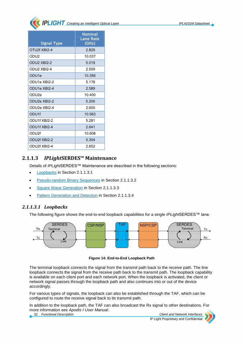
Creating an Intelligent Optical Layer IPL4101M Datasheet
32 Functional Description Client and Network Interfaces
IP Light Proprietary and Confidential
Signal Type
Nominal Lane Rate
(GHz)
OTU2f XBI2-4 2.829
ODU2 10.037
ODU2 XBI2-2 5.019
ODU2 XBI2-4 2.509
ODU1e 10.356
ODU1e XBI2-2 5.178
ODU1e XBI2-4 2.589
ODU2e 10.400
ODU2e XBI2-2 5.200
ODU2e XBI2-4 2.600
ODU1f 10.563
ODU1f XBI2-2 5.281
ODU1f XBI2-4 2.641
ODU2f 10.608
ODU2f XBI2-2 5.304
ODU2f XBI2-4 2.652
2.1.1.3 IPLightSERDES™ Maintenance
Details of IPLightSERDES™ Maintenance are described in the following sections:
Loopbacks in Section 2.1.1.3.1
Pseudo-random Binary Sequences in Section 2.1.1.3.2
Square Wave Generation in Section 2.1.1.3.3
Pattern Generation and Detection in Section 2.1.1.3.4
2.1.1.3.1 Loopbacks
The following figure shows the end-to-end loopback capabilities for a single IPLightSERDES™ lane.
TAFCSP/NSP NSP/CSPSERDES SERDESTxRx
RxTx
Terminal Terminal
LineLine
Figure 14: End-to-End Loopback Path
The terminal loopback connects the signal from the transmit path back to the receive path. The line loopback connects the signal from the receive path back to the transmit path. The loopback capability is available on each client port and each network port. When the loopback is activated, the client or network signal passes through the loopback path and also continues into or out of the device accordingly.
For various types of signals, the loopback can also be established through the TAF, which can be configured to route the receive signal back to its transmit path.
In addition to the loopback path, the TAF can also broadcast the Rx signal to other destinations. For more information see Apodis I User Manual.
Creating an Intelligent Optical Layer IPL4101M Datasheet
33 Functional Description Client and Network Interfaces
IP Light Proprietary and Confidential
2.1.1.3.2 Pseudo-random Binary Sequences
The IPL4101M provides Pseudo-Random Binary Sequence (PRBS) test signal generation on the transmit path of all of the client and network ports. Corresponding integrated PRBS monitoring is provided on the receive path of each port. The following test pseudo-random binary sequences are available:
PRBS7
PRBS7 is a proprietary sequence based on the polynomial x7+x6+1.
PRBS9
PRBS15
PRBS23
PRBS31
These test signals are defined in ITU-T O.150. For more information, refer to ITU-T Series O: Specifications of Measuring Equipment in the following recommendations:
PRBS9: O.150 Section 5.1 and O.153
PRBS15: O.150 Section 5.3 and O.151
PRBS23: O.150 Section 5.6 and O.151
PRBS31: O.150 Section 5.8.
2.1.1.3.3 Square Wave Generation
The IPL4101M can generate a square wave signal on its interfaces, which can be used to conduct measurements on optical signals. The square wave is generated by a user-defined number of ones (1) followed by the same number of zeros (0). For more information about specific programming instructions for square wave generation, refer to the Apodis I User Manual. For more information about square wave signal generation, refer to IEEE 802 Part 3: Carrier Sense Multiple Access with Collision Detection (CSMA/CD) Access Method and Physical Layer Specifications, Chapter 49.
2.1.1.3.4 Pattern Generation and Detection
The IPL4101M can generate, on any of its ports, a user-defined 40 bit pattern. This pattern is transmitted continuously and can be monitored on the Rx side of the IPL4101M by an integrated detector. For more information about specific programming instructions for pattern generation and detection, refer to the Apodis I User Manual.
2.1.2 Serial Interface
Network and client side ports support serial (single lane) interfaces that can operate with signals from 125 Mbps up to 11.4 Gbps signal rates. The network side ports support XFI and SFP+ interfaces and the client side ports support XFI, SFP+, and SFP interfaces. A serial XFI interface operating at 10Gbps can drive signals up to 12 inches through standard FR4 material. The interfaces conform to the XFI and SFP specifications.
NOTE—XFI specification: INF-8077i, 10 Gigabit Small Form Factor Pluggable Module, Revision 4.5 August 31, 2005.
NOTE—SFP Revision 1.0, Small Form-factor Pluggable (SFP) Transceiver MultiSource Agreement (MSA).

Creating an Intelligent Optical Layer IPL4101M Datasheet
34 Functional Description Client and Network Interfaces
IP Light Proprietary and Confidential
2.1.3 XBI2
The IPL4101M offers a special OTU2/ODU2 interface on both its client and network ports called XBI2. While being similar to MLD, it is adapted for 10Gbps signal rates. XBI2 carries OTU2/ODU2 signals over a two-lane (XBI2-2) or four -lane (XBI2-4) parallel interface. XBI2-2 has two lanes, each running at half the respective OTU2/ODU2 rate, and XBI2-4 has four lanes, each running at a quarter of the respective OTU2/ODU2 rate. XBI2 interfaces can drive signals directly across backplanes or be used to interface with FPGAs. When OTU2 signals are carried over XBI2 interfaces, the OTU2 FEC can optionally be activated to provide further enhanced signal integrity.
The following figure shows how OTU2x/ODU2x frames are being inversely multiplexed over XBI2-4 lanes, the 16-byte boundaries and their respective alignment with the OTU2x/ODU2x frames.
Figure 15: XBI2-4 Lane Assignments
Each 16 byte section is sequentially distributed to each of the lanes. On the frame boundary, the lane assignments are rotated.
The following table describes the lane assignment as determined by the two LSB bits of the MFAS of the OTU2/ODU2 for XBI2-4.
Table 15: OTU2/ODU2 Information Lane Assignment for XBI2-4
MFAS bits 7,8 Lane 0 Lane 1 Lane 2 Lane 3
00 1:16 17:32 33:48 49:64
01 49:64 1:16 17:32 33:48
10 33:48 49:64 1:16 17:32
11 17:32 33:48 49:64 1:16
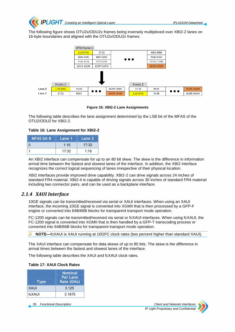
Creating an Intelligent Optical Layer IPL4101M Datasheet
35 Functional Description Client and Network Interfaces
IP Light Proprietary and Confidential
The following figure shows OTU2x/ODU2x frames being inversely multiplexed over XBI2-2 lanes on 16-byte boundaries and aligned with the OTU2x/ODU2x frames.
Figure 16: XBI2-2 Lane Assignments
The following table describes the lane assignment determined by the LSB bit of the MFAS of the OTU2/ODU2 for XBI2-2.
Table 16: Lane Assignment for XBI2-2
MFAS bit 8 Lane 1 Lane 2
0 1:16 17:32
1 17:32 1:16
An XBI2 interface can compensate for up to an 80 bit skew. The skew is the difference in information arrival time between the fastest and slowest lanes of the interface. In addition, the XBI2 interface recognizes the correct logical sequencing of lanes irrespective of their physical location.
XBI2 interfaces provide improved drive capability. XBI2-2 can drive signals across 24 inches of standard FR4 material. XBI2-4 is capable of driving signals across 30 inches of standard FR4 material including two connector pairs, and can be used as a backplane interface.
2.1.4 XAUI Interface
10GE signals can be transmitted/received via serial or XAUI interfaces. When using an XAUI interface, the incoming 10GE signal is converted into XGMII that is then processed by a GFP-F engine or converted into 64B/66B blocks for transparent transport mode operation.
FC-1200 signals can be transmitted/received via serial or fcXAUI interfaces. When using fcXAUI, the FC-1200 signal is converted into XGMII that is then handled by a GFP-T transcoding process or converted into 64B/66B blocks for transparent transport mode operation.
NOTE—fcXAUI is XAUI running at 10GFC clock rates (two percent higher than standard XAUI).
The XAUI interface can compensate for data skews of up to 80 bits. The skew is the difference in arrival times between the fastest and slowest lanes of the interface.
The following table describes the XAUI and fcXAUI clock rates.
Table 17: XAUI Clock Rates
Type
Nominal Per Lane
Rate (GHz)
XAUI 3.125
fcXAUI 3.1875
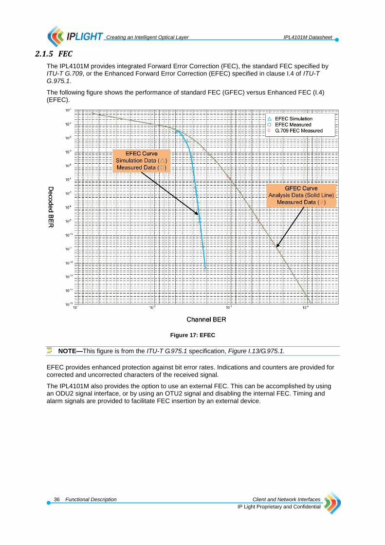
Creating an Intelligent Optical Layer IPL4101M Datasheet
36 Functional Description Client and Network Interfaces
IP Light Proprietary and Confidential
2.1.5 FEC
The IPL4101M provides integrated Forward Error Correction (FEC), the standard FEC specified by ITU-T G.709, or the Enhanced Forward Error Correction (EFEC) specified in clause I.4 of ITU-T G.975.1.
The following figure shows the performance of standard FEC (GFEC) versus Enhanced FEC (I.4) (EFEC).
Figure 17: EFEC
NOTE—This figure is from the ITU-T G.975.1 specification, Figure I.13/G.975.1.
EFEC provides enhanced protection against bit error rates. Indications and counters are provided for corrected and uncorrected characters of the received signal.
The IPL4101M also provides the option to use an external FEC. This can be accomplished by using an ODU2 signal interface, or by using an OTU2 signal and disabling the internal FEC. Timing and alarm signals are provided to facilitate FEC insertion by an external device.
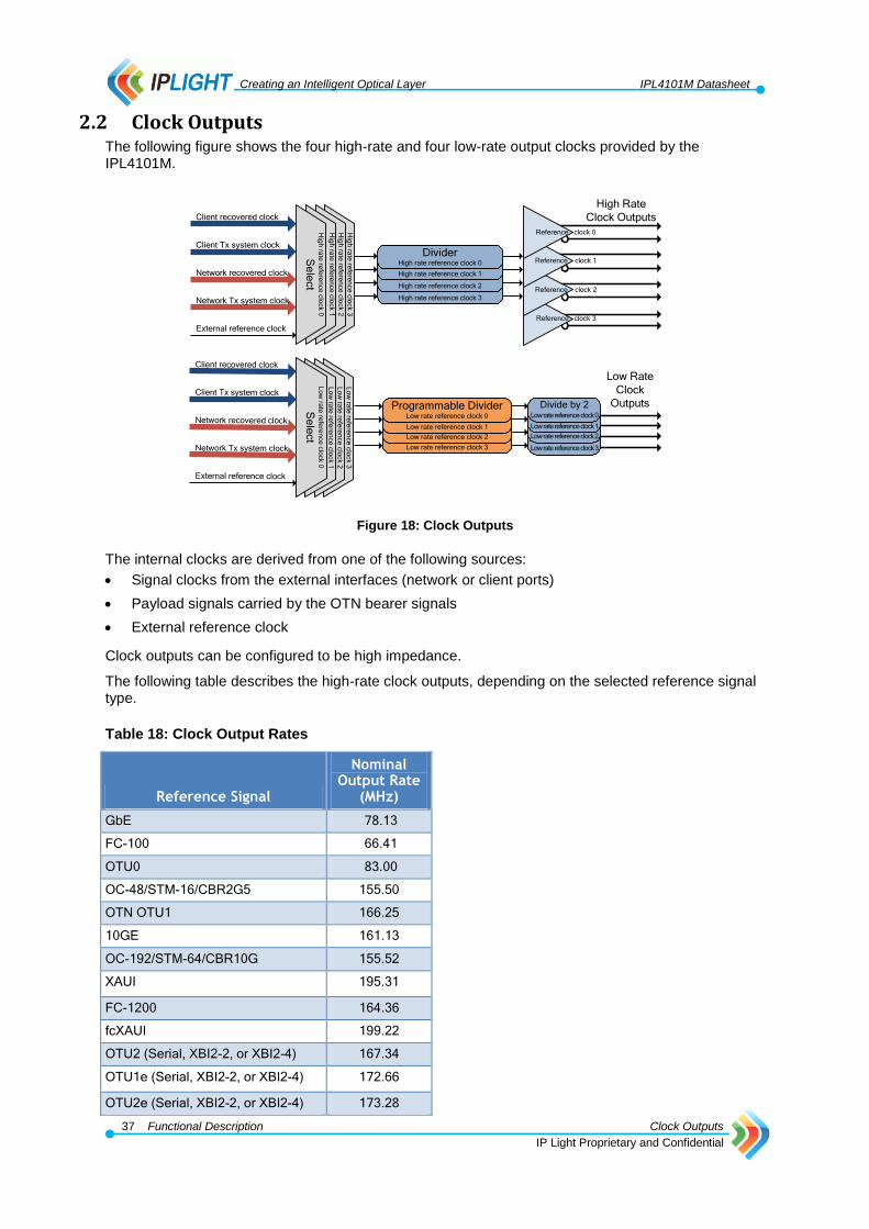
Creating an Intelligent Optical Layer IPL4101M Datasheet
37 Functional Description Clock Outputs
IP Light Proprietary and Confidential
2.2 Clock Outputs The following figure shows the four high-rate and four low-rate output clocks provided by the IPL4101M.
Low Rate
Clock
Outputs
Divide by 2Low rate reference clock 3
Divide by 2Low rate reference clock 2
Divide by 2Low rate reference clock 1
Programmable DividerLow rate reference clock 3
Programmable DividerLow rate reference clock 2
Programmable DividerLow rate reference clock 1
DividerHigh rate reference clock 3
DividerHigh rate reference clock 2
DividerHigh rate reference clock 1
Lo
w ra
te re
fere
nce
clo
ck 3
Lo
w ra
te re
fere
nce
clo
ck 2
Lo
w ra
te re
fere
nce
clo
ck 1
Client recovered clock
Network recovered clock
DividerHigh rate reference clock 0
Lo
w ra
te re
fere
nce
clo
ck 0
Se
lect
Programmable DividerLow rate reference clock 0
External reference clock
Client Tx system clock
Network Tx system clock
Client recovered clock
Network recovered clock
External reference clock
Client Tx system clock
Network Tx system clock
Divide by 2Low rate reference clock 0
Hig
h ra
te re
fere
nce
clo
ck 3
Hig
h ra
te re
fere
nce
clo
ck 2
Hig
h ra
te re
fere
nce
clo
ck 1
Hig
h ra
te re
fere
nce
clo
ck 0
Se
lect
Reference clock 1
Reference clock 0
High Rate
Clock Outputs
Reference clock 2
Reference clock 3
Figure 18: Clock Outputs
The internal clocks are derived from one of the following sources:
Signal clocks from the external interfaces (network or client ports)
Payload signals carried by the OTN bearer signals
External reference clock
Clock outputs can be configured to be high impedance.
The following table describes the high-rate clock outputs, depending on the selected reference signal type.
Table 18: Clock Output Rates
Reference Signal
Nominal Output Rate
(MHz)
GbE 78.13
FC-100 66.41
OTU0 83.00
OC-48/STM-16/CBR2G5 155.50
OTN OTU1 166.25
10GE 161.13
OC-192/STM-64/CBR10G 155.52
XAUI 195.31
FC-1200 164.36
fcXAUI 199.22
OTU2 (Serial, XBI2-2, or XBI2-4) 167.34
OTU1e (Serial, XBI2-2, or XBI2-4) 172.66
OTU2e (Serial, XBI2-2, or XBI2-4) 173.28

Creating an Intelligent Optical Layer IPL4101M Datasheet
38 Functional Description External Overhead Interface
IP Light Proprietary and Confidential
Reference Signal
Nominal Output Rate
(MHz)
OTU1f (Serial, XBI2-2, or XBI2-4) 176.09
OTU2f (Serial, XBI2-2, or XBI2-4) 176.88
ODU2 (Serial, XBI2-2, or XBI2-4) 156.88
ODU1e (Serial, XBI2-2, or XBI2-4) 161.88
ODU2e (Serial, XBI2-2, or XBI2-4) 162.50
ODU1f (Serial, XBI2-2, or XBI2-4) 165.00
ODU2f (Serial, XBI2-2, or XBI2-4) 165.78
External reference clock 155.52
For low-rate clock outputs the selected reference signal rate is divided by a 16 bit configurable counter and is then further divided by two (2) to generate clock signals of frequencies of up to 100MHz. If the configurable counter is not used, then the low-rate is half the nominal high-rate output frequency of the selected reference signal rate shown in the table Clock Output Rates (above).
For more information about clock signals and parameters, see Clock Signals Interface in Section 1.1.4
and Clock Parameters in Section 4.7.
2.3 External Overhead Interface
The External Overhead Interface (EOI) provides access to received OverHead (OH) bytes through the RxOHD data bus and provides access to the transmitted OH bytes through the TxOHD data bus. Per byte selection of TxOHD data between internal and external data sources is set by configuring a bit in its corresponding register. Access is provided to all active OTN (OTU1/2, ODU0/1/2, and OPU0/1/2) OH bytes, and also to SONET/SDH section DCC, order wire (E1), and user defined F1 channel.
Each individual OTN and SONET/SDH signal has been assigned an associated OH block. For OTN signals, this block consists of 64 bytes of OH information and for SONET/SDH signals it consists of the F1, E1, and DCC bytes. The following figure shows how the EOI operates continuously and sequentially cycles through the OH blocks in the IPL4101M.
EOI
NSP3
CSP3CSP2
CSP1
Data Out
(RxOHD[15:0])
Data Valid
(RxOHVLD)
Round robin
NSP2
OD
U0
OH
OD
U0
OH
OD
U0
OH
OD
U0
OH
OD
U0
OH
OD
U0
OH
OD
U0
OH
OD
U0
OH
OD
U1
OH
OD
U1
OH
OD
U1
OH
OD
U1
OH
OD
U2
OH
Data In
(TxOHD[15:0])
CSP0
OD
U1
OH
OD
U1
OH
OD
U1
OH
OD
U1
OH
OD
U2
OH
OC
-48 O
H O
C-4
8 OH
OC
-48 O
H O
C-4
8 OH
OC
-192
OH
OHCID[9:0] OHCLK
Timeslot number
OH Request
(TxOHRQ)
TxOHMFAS
Figure 19: External Overhead Interface
Each overhead block is represented by a timeslot with an associated channel number. During each timeslot the complete OH block of any signal can be both read out and modified (written to) through the EOI.

Creating an Intelligent Optical Layer IPL4101M Datasheet
39 Functional Description External Overhead Interface
IP Light Proprietary and Confidential
The following figure shows an OTN signal data insertion/flow between the EOI and the Tx side overheads.
OTU
ODU
OPU
Control
Register
OH Control
Register
OH Insertion FEC Scrambler
Selector
External Overhead
Interface
Internal OHGenerator
Tx EOI
OHHandler
Figure 20: EOI OTN Insertion
For OH data insertion, the Tx OH block bytes can be overwritten through the TxOHD bus. Data must be written when the appropriate channel number (OHCID) is present and TxOHRQ is active. The data of Tx OH blocks configured for internal handling overrides the OH bytes received from the data path. The TX OH request signal (TxOHRQ) indicates that the IPL4101M requests OH data for transmission. There is also an MFAS signal (TxOHMFAS) that indicates the multiframe alignment for the selected Tx signal. A TxOHMFAS signal is provided for each overhead channel (according to the respective OHCID channel number). When TxOHMFAS is high it indicates the start of a new multiframe for the current channel. Accordingly, the TxOHMFAS signal associated with the particular channel remains high for the complete transaction for frame 0 and is low for the next 255 consecutive channel frames.
The following figure shows an OTN signal data extraction/flow between the EOI and the Rx side overheads.
OTU
ODU
OPU
Rx OH
Capture
OH Handler
External Overhead
Interface
Indication
Rx EOI
FEC ScramblerOTU
Framer
Figure 21: EOI OTN Extraction
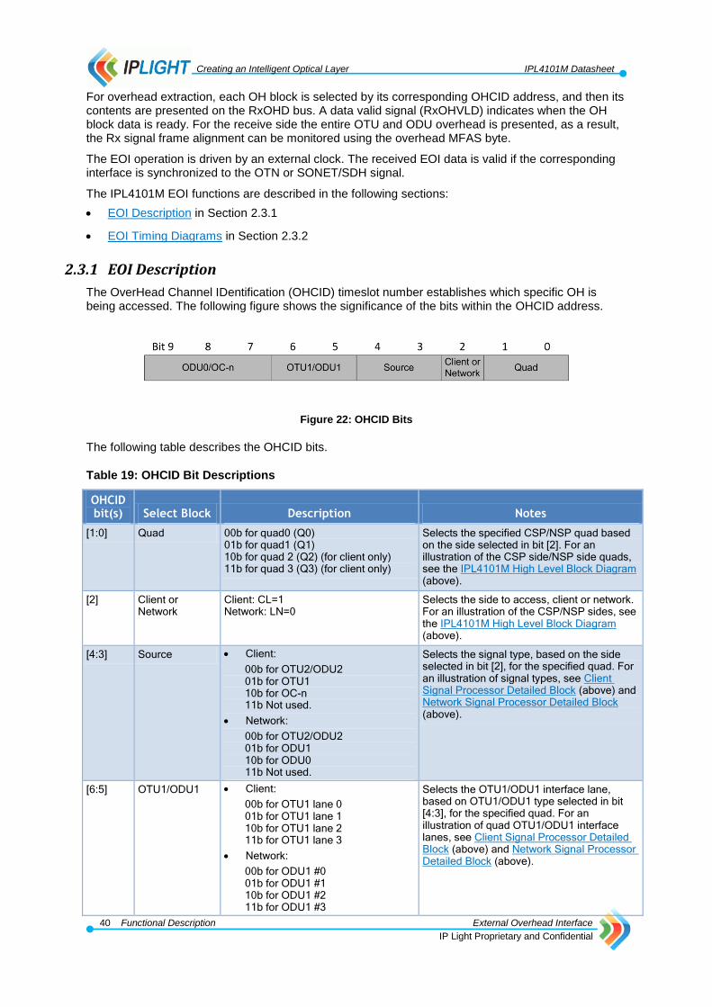
Creating an Intelligent Optical Layer IPL4101M Datasheet
40 Functional Description External Overhead Interface
IP Light Proprietary and Confidential
For overhead extraction, each OH block is selected by its corresponding OHCID address, and then its contents are presented on the RxOHD bus. A data valid signal (RxOHVLD) indicates when the OH block data is ready. For the receive side the entire OTU and ODU overhead is presented, as a result, the Rx signal frame alignment can be monitored using the overhead MFAS byte.
The EOI operation is driven by an external clock. The received EOI data is valid if the corresponding interface is synchronized to the OTN or SONET/SDH signal.
The IPL4101M EOI functions are described in the following sections:
EOI Description in Section 2.3.1
EOI Timing Diagrams in Section 2.3.2
2.3.1 EOI Description
The OverHead Channel IDentification (OHCID) timeslot number establishes which specific OH is being accessed. The following figure shows the significance of the bits within the OHCID address.
Figure 22: OHCID Bits
The following table describes the OHCID bits.
Table 19: OHCID Bit Descriptions
OHCID bit(s) Select Block Description Notes
[1:0] Quad 00b for quad0 (Q0) 01b for quad1 (Q1) 10b for quad 2 (Q2) (for client only) 11b for quad 3 (Q3) (for client only)
Selects the specified CSP/NSP quad based on the side selected in bit [2]. For an illustration of the CSP side/NSP side quads, see the IPL4101M High Level Block Diagram (above).
[2] Client or Network
Client: CL=1 Network: LN=0
Selects the side to access, client or network. For an illustration of the CSP/NSP sides, see the IPL4101M High Level Block Diagram (above).
[4:3] Source Client:
00b for OTU2/ODU2 01b for OTU1 10b for OC-n 11b Not used.
Network:
00b for OTU2/ODU2 01b for ODU1 10b for ODU0 11b Not used.
Selects the signal type, based on the side selected in bit [2], for the specified quad. For an illustration of signal types, see Client Signal Processor Detailed Block (above) and Network Signal Processor Detailed Block (above).
[6:5] OTU1/ODU1 Client:
00b for OTU1 lane 0 01b for OTU1 lane 1 10b for OTU1 lane 2 11b for OTU1 lane 3
Network:
00b for ODU1 #0 01b for ODU1 #1 10b for ODU1 #2 11b for ODU1 #3
Selects the OTU1/ODU1 interface lane, based on OTU1/ODU1 type selected in bit [4:3], for the specified quad. For an illustration of quad OTU1/ODU1 interface lanes, see Client Signal Processor Detailed Block (above) and Network Signal Processor Detailed Block (above).

Creating an Intelligent Optical Layer IPL4101M Datasheet
41 Functional Description External Overhead Interface
IP Light Proprietary and Confidential
OHCID bit(s) Select Block Description Notes
[9:7] ODU0/OC-n Client:
000b for OC-192 001b for OC-48 lane 0 010b for OC-48 lane 1 011b for OC-48 lane 2 100b for OC-48 lane 3 101b Reserved 110b Reserved 111b Reserved
Network:
000b for ODU0 #0 001b for ODU0 #1 010b for ODU0 #2 011b for ODU0 #3 100b for ODU0 #4 101b for ODU0 #5 110b for ODU0 #6 111b for ODU0 #7
Selects the OC-n/ODU0 signal, based on OC-n/ODU0 source selected in bit [4:3], for the specified quad. For an illustration of quad OC-n/ODU0 signals, see Client Signal Processor Detailed Block (above) and Network Signal Processor Detailed Block (above).
For an illustration of the layout of the client/network side blocks, see High Level System Description in
Section 1.
The following examples illustrate how the OHCID is decoded:
If the OHCID is 1111101101b decode it as follows:
Bits [1:0] are 01b, designating quad 1 Bit [2] is 1, designating the client side Bits [4:3] are 01b, designating OTU1/ODU1 Bits [6:5] are 11b, designating the #3 OTU1/ODU1 as OH Bits [9:7] are not significant because theODU0/OC-n field is set to 111b
The OH block being accessed corresponds to the #3 OTU1 or ODU1 from quad 1 of the client side.
If the OHCID is 0011110111 decode it as follows:
Bits [1:0] are 11b, designating quad 3 Bit [2] is 1, designating the client side Bits [4:3] are 10b, designating OC-n Bits [6:5] are not significant because the type is OC-n Bits [9:7] are 001b, designating the #0 OC-48 OH
The OH block, which is being accessed, corresponds to an OC-48 signal on lane 0 from quad 3 of the client side.
The following figure shows the 64 byte OH of an OTN signal.
OTN OH
FASRow 1
Row 2
Row 3
Row 4
Column 1
MFAS SM GCC0 RESERVED RESERVED RESERVED JCA
RESERVED RESERVED RESERVED TCM ACT TCM6 TCM5 TCM4 FTFL RESERVED JCB
TCM3 TCM2 TCM1 PM EXP RESERVED RESERVED NJO2
GCC1 GCC2 APS/PCC RESERVED RESERVED RESERVED RESERVED RESERVED RESERVED PSI NJO1
2 3 4 5 6 7 8 9 10 11 12 13 14 15 16
Figure 23: OTN OH Structure
The transmitted and received overhead data busses are 16 bits wide. The overhead information of the selected OTN signal is presented on the data bus two bytes at a time starting with the column 1 and 2 of the first OTN row and proceeding sequentially to the end of the OH row and then moving over to the next sequential row. Each two bytes of the OH data are assigned on the data bus as follows:
Bit 15 of the OH bus corresponds to the first bit received from the odd column of the OTN OH
Bit 0 corresponds to the last received bit of the even column
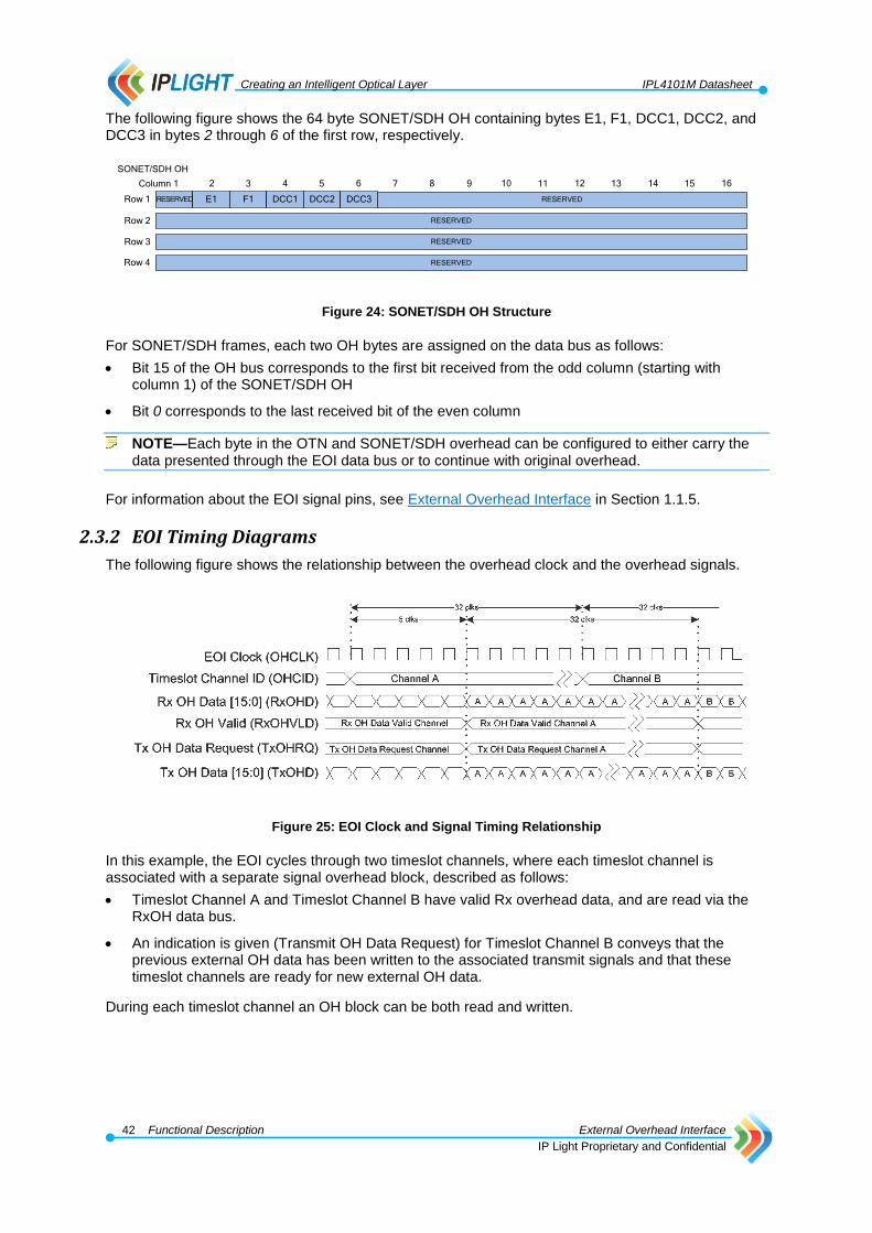
Creating an Intelligent Optical Layer IPL4101M Datasheet
42 Functional Description External Overhead Interface
IP Light Proprietary and Confidential
The following figure shows the 64 byte SONET/SDH OH containing bytes E1, F1, DCC1, DCC2, and DCC3 in bytes 2 through 6 of the first row, respectively.
SONET/SDH OH
Row 1
Row 2
Row 3
Row 4
Column 1 2 3 4 5 6 7 8 9 10 11 12 13 14 15 16
RESERVED E1 F1 DCC1 DCC2 DCC3 RESERVED
RESERVED
RESERVED
RESERVED
Figure 24: SONET/SDH OH Structure
For SONET/SDH frames, each two OH bytes are assigned on the data bus as follows:
Bit 15 of the OH bus corresponds to the first bit received from the odd column (starting with column 1) of the SONET/SDH OH
Bit 0 corresponds to the last received bit of the even column
NOTE—Each byte in the OTN and SONET/SDH overhead can be configured to either carry the data presented through the EOI data bus or to continue with original overhead.
For information about the EOI signal pins, see External Overhead Interface in Section 1.1.5.
2.3.2 EOI Timing Diagrams
The following figure shows the relationship between the overhead clock and the overhead signals.
Figure 25: EOI Clock and Signal Timing Relationship
In this example, the EOI cycles through two timeslot channels, where each timeslot channel is associated with a separate signal overhead block, described as follows:
Timeslot Channel A and Timeslot Channel B have valid Rx overhead data, and are read via the RxOH data bus.
An indication is given (Transmit OH Data Request) for Timeslot Channel B conveys that the previous external OH data has been written to the associated transmit signals and that these timeslot channels are ready for new external OH data.
During each timeslot channel an OH block can be both read and written.

Creating an Intelligent Optical Layer IPL4101M Datasheet
43 Functional Description Host Processor Interface
IP Light Proprietary and Confidential
The following figure shows the timing of the MFAS signal (TxOHMFAS) indicating the multiframe alignment for the selected Tx signal.
Figure 26: TxMFAS Timing
In this example, a TxOHMFAS signal is provided for each overhead channel (according to the respective OHCID channel number). When TxOHMFAS is high it indicates the start of a new multiframe for the current channel. Accordingly, the TxOHMFAS signal associated with the particular channel remains high for the complete transaction for frame 0 and is low for the next 255 consecutive channel frames.
For more information about EOI timing, see EOI Characteristics in Section 4.4.
2.4 Host Processor Interface
The IPL4101M includes a generic synchronous Host Processor Interface (HPI), which enables the user to configure all the various operational modes of the IPL4101M and monitor Client and Network signal status and performance. The operation and configuration of the IPL4101M is performed by writing to and reading from internal registers using the HPI. This interface facilitates quick setup, easy status monitoring, and allows the IPL4101M to interface with the host processor.
The IPL4101M HPI is described in the following sections:
HPI Description in Section 2.4.1
HPI Freescale Mode in Section 2.4.2
HPI Intel Mode in Section 2.4.3
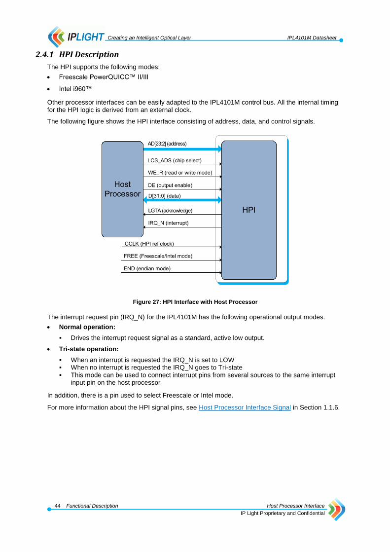
Creating an Intelligent Optical Layer IPL4101M Datasheet
44 Functional Description Host Processor Interface
IP Light Proprietary and Confidential
2.4.1 HPI Description
The HPI supports the following modes:
Freescale PowerQUICC™ II/III
Intel i960™
Other processor interfaces can be easily adapted to the IPL4101M control bus. All the internal timing for the HPI logic is derived from an external clock.
The following figure shows the HPI interface consisting of address, data, and control signals.
D[31:0] (data)
AD[23:2] (address)
HPI
END (endian mode)
FREE (Freescale/Intel mode)
CCLK (HPI ref clock)
LCS_ADS (chip select)
IRQ_N (interrupt)
LGTA (acknowledge)
WE_R (read or write mode)
OE (output enable)Host
Processor
Figure 27: HPI Interface with Host Processor
The interrupt request pin (IRQ_N) for the IPL4101M has the following operational output modes.
Normal operation:
Drives the interrupt request signal as a standard, active low output.
Tri-state operation:
When an interrupt is requested the IRQ_N is set to LOW When no interrupt is requested the IRQ_N goes to Tri-state This mode can be used to connect interrupt pins from several sources to the same interrupt
input pin on the host processor
In addition, there is a pin used to select Freescale or Intel mode.
For more information about the HPI signal pins, see Host Processor Interface Signal in Section 1.1.6.

Creating an Intelligent Optical Layer IPL4101M Datasheet
45 Functional Description Host Processor Interface
IP Light Proprietary and Confidential
2.4.2 Freescale Mode
Read timing cycles
The following figure shows the Freescale mode read timing.
Figure 28: Freescale Interface Read Timing Cycle
When data is read through the HPI the chip select (LCS_ADS) is set low and the address of the IPL4101M register to be read is presented on the AD bus. When the host processor receives the acknowledge strobe (LGTA), it responds with an appropriate output enable pulse (OE low) and the data can be read through the bus.
The address and control signals must remain valid for the length of the read cycle of 14 clock cycles (four of the clock cycles are for reads from global module registers) until the host processor receives from the IPL4101M the LGTA strobe, which indicates the end of the read operation. The next read operation can start two clock cycles after the LGTA strobe is received by the host processor.
NOTE—For high CCLK frequencies, Data (D) removal from the bus after Output Enable (OE) high may take longer than a single CCLK cycle. On these events Freescale relaxed mode can be
considered. For more information about HPI timing, see HPI Characteristics in Section 4.5. For
more information about Freescale relaxed mode, refer to Freescale documentation.
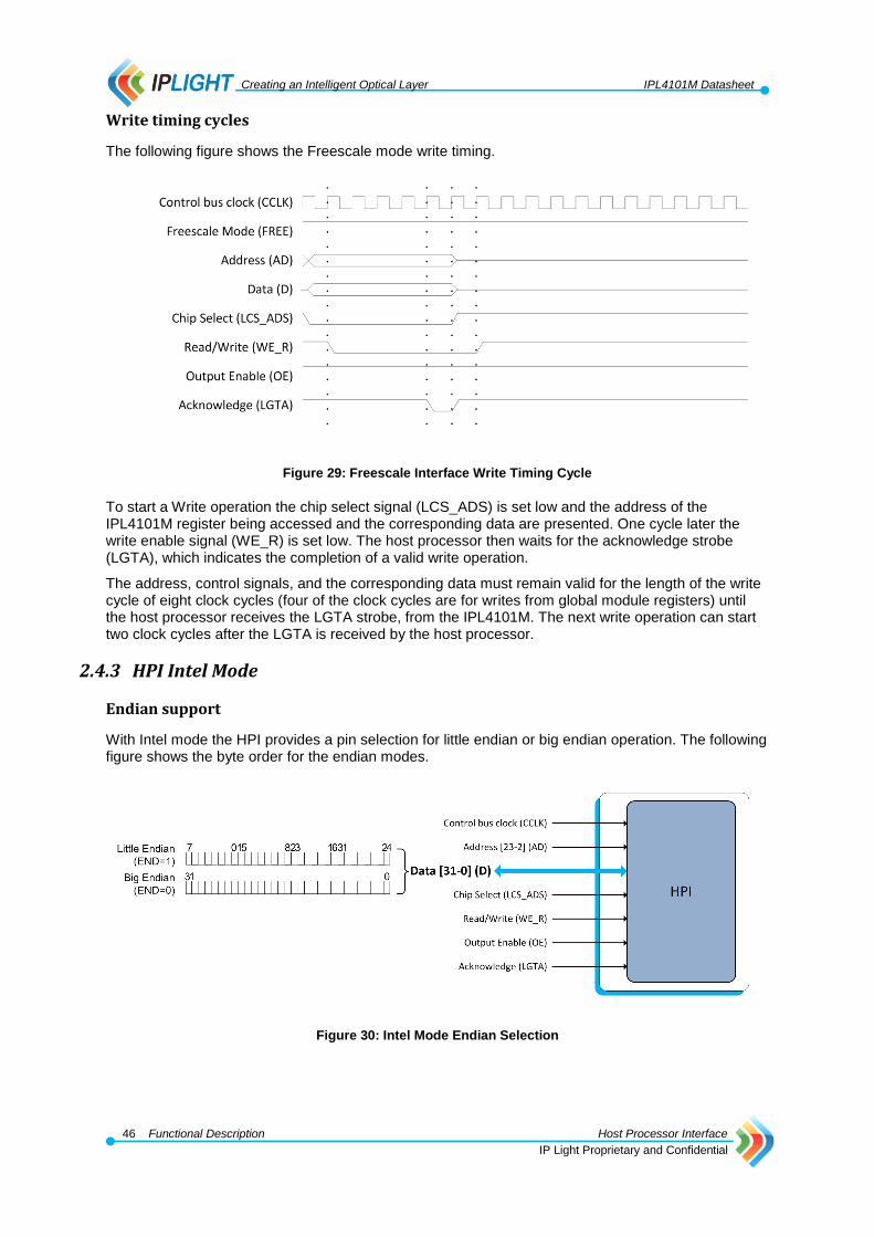
Creating an Intelligent Optical Layer IPL4101M Datasheet
46 Functional Description Host Processor Interface
IP Light Proprietary and Confidential
Write timing cycles
The following figure shows the Freescale mode write timing.
Figure 29: Freescale Interface Write Timing Cycle
To start a Write operation the chip select signal (LCS_ADS) is set low and the address of the IPL4101M register being accessed and the corresponding data are presented. One cycle later the write enable signal (WE_R) is set low. The host processor then waits for the acknowledge strobe (LGTA), which indicates the completion of a valid write operation.
The address, control signals, and the corresponding data must remain valid for the length of the write cycle of eight clock cycles (four of the clock cycles are for writes from global module registers) until the host processor receives the LGTA strobe, from the IPL4101M. The next write operation can start two clock cycles after the LGTA is received by the host processor.
2.4.3 HPI Intel Mode
Endian support
With Intel mode the HPI provides a pin selection for little endian or big endian operation. The following figure shows the byte order for the endian modes.
Figure 30: Intel Mode Endian Selection

Creating an Intelligent Optical Layer IPL4101M Datasheet
47 Functional Description Host Processor Interface
IP Light Proprietary and Confidential
Read timing cycles
The following figure shows the Intel mode read cycles.
Figure 31: Intel Interface Read Timing Cycle
The Read data pin (LCS_ADS) is strobed low for one clock cycle. One cycle later the address of the IPL4101M internal register to be read is presented, while the output enable signal (OE) is set low. When the host processor receives the acknowledge (LGTA) indication pulse, valid data can be read through the data bus.
The address and control signals must remain valid until the host processor receives the LGTA signal, which requires up to 15 cycles for read. The next read operation can start two clock cycles after the LGTA is received by the host processor.
NOTE—For high CCLK frequencies, data (D) removal from the bus after otput enable (OE) high may take longer than a single CCLK cycle. For more information about HPI timing, see HPI
Characteristics in Section 4.5.
Write timing cycles
The following figure shows the Intel mode write cycles.
Figure 32: Intel Interface Write Timing Cycle

Creating an Intelligent Optical Layer IPL4101M Datasheet
48 Functional Description JTAG Interface
IP Light Proprietary and Confidential
The write data signal (LCS_ADS) is strobed low for one clock cycle. One cycle later the address of the IPL4101M internal register, the data bus, and the write enable (WE_R) signal are all presented with valid signals. The host processor then waits for the IPL4101M to generate a corresponding acknowledge (LGTA) strobe, which indicates that a valid write operation has been accomplished.
The address, controls signals, and data information must remain valid for nine clock cycles until the host processor receives the LGTA strobe from the IPL4101M. The next write operation can start two clock cycles after the LGTA is received by the host processor.
2.5 JTAG Interface
The IPL4101M supports JTAG IEEE Std 1149.1-1990, IEEE Standard Test Access Port and
Boundary. For information about JTAG timing values, see JTAG Characteristics in Section 4.6.

Creating an Intelligent Optical Layer IPL4101M Datasheet
49 Design Considerations
IP Light Proprietary and Confidential
3 Design Considerations IPL4101M design considerations are described in the following sections:
IPLightSERDES™ Interface in Section 3.1
Reference Clock in Section 3.2
Power and Ground Connections in Section 3.3
Package Information in Section 3.4
3.1 IPLightSERDES™ Interface
The following figure shows the IPLightSERDES™ external connections.
Figure 33: IPLightSERDES™ Interface
The IPL4101M can drive signals through standard FR4 material. The following table describes the IPLightSERDES™ output drive capabilities over different lane rates.
Table 20: Output Drive Capability
Interface Rate
Maximum Trace Length for Standard FR4 Material
(inches) Notes
11.4Gbps 12
5.7Gbps 24
3.2Gbps 30 Including two connectors in backplane interconnect.
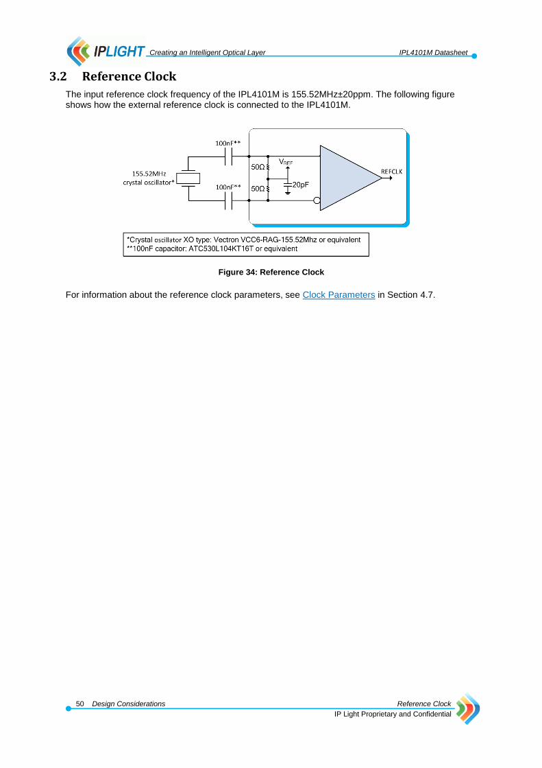
Creating an Intelligent Optical Layer IPL4101M Datasheet
50 Design Considerations Reference Clock
IP Light Proprietary and Confidential
3.2 Reference Clock
The input reference clock frequency of the IPL4101M is 155.52MHz±20ppm. The following figure shows how the external reference clock is connected to the IPL4101M.
Figure 34: Reference Clock
For information about the reference clock parameters, see Clock Parameters in Section 4.7.
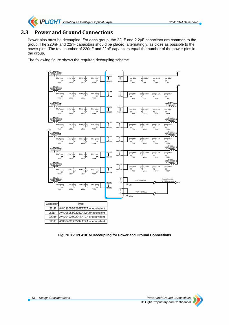
Creating an Intelligent Optical Layer IPL4101M Datasheet
51 Design Considerations Power and Ground Connections
IP Light Proprietary and Confidential
3.3 Power and Ground Connections
Power pins must be decoupled. For each group, the 22μF and 2.2μF capacitors are common to the group. The 220nF and 22nF capacitors should be placed, alternatingly, as close as possible to the power pins. The total number of 220nF and 22nF capacitors equal the number of the power pins in the group.
The following figure shows the required decoupling scheme.
Figure 35: IPL4101M Decoupling for Power and Ground Connections
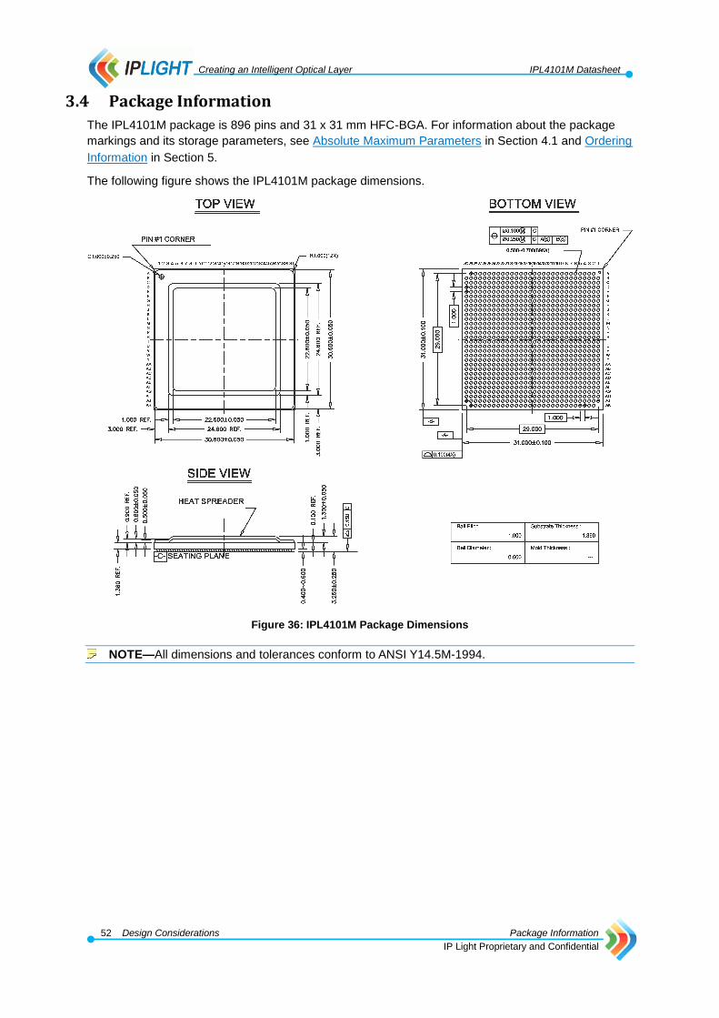
Creating an Intelligent Optical Layer IPL4101M Datasheet
52 Design Considerations Package Information
IP Light Proprietary and Confidential
3.4 Package Information
The IPL4101M package is 896 pins and 31 x 31 mm HFC-BGA. For information about the package
markings and its storage parameters, see Absolute Maximum Parameters in Section 4.1 and Ordering
Information in Section 5.
The following figure shows the IPL4101M package dimensions.
Figure 36: IPL4101M Package Dimensions
NOTE—All dimensions and tolerances conform to ANSI Y14.5M-1994.

Creating an Intelligent Optical Layer IPL4101M Datasheet
53 Electrical and Mechanical Data Absolute Maximum Ratings
IP Light Proprietary and Confidential
4 Electrical and Mechanical Data The IPL4101M has two input voltages, 1.0V and 2.5V. The IPL4101M operates at 1.0V ±5% and 2.5V ±5%, unless otherwise specified.
IPL4101M electrical and mechanical characteristics are described in the following sections:
Absolute Maximum Ratings in Section 4.1
Normal Operating Conditions in Section 4.2
High Speed Differential IO Characteristics in Section 4.3
EOI Characteristics in Section 4.4
HPI Characteristics in Section 4.5
JTAG Characteristics in Section 4.6
Output Reference Clock Parameters in Section 4.7
Reset Signal Parameters in Section 4.8
Thermal Information in Section 4.9
Power in Section 4.10
4.1 Absolute Maximum Ratings
WARNING—Permanent device damage may occur if the Absolute Maximum Ratings are
exceeded.
CAUTION—Exposure to absolute maximum rating conditions for extended periods of time may
affect device reliability.
The following table describes the maximum limits that the IPL4101M can withstand without sustaining permanent damage. These limits are not indicative of normal mode operation conditions.
Table 21: Absolute Maximum Ratings
Description Limits
Voltage 1.0V (VDD10, VDD10A/B/C/D/E/F) -0.3V to 1.35V
Voltage 2.5V (VDD25, VDD25A/B/C) -0.3V to 3V
Static discharge voltage ±2000V (±1000 V for low voltage CML and low voltage PECL differential pins)
Storage temperature -40°C to 125°C
Lead temperature 230°C
Case temperature under bias -40°C to 105°C
Absolute maximum junction temperature 150°C
DC input current ±20 mA
Voltage on Digital Input or Bidirectional Pin -0.3V to 3.6V
Voltage on any digital output pin -0.3V to (VDD25+0.3 V)
Voltage on any differential pin -0.3V to (VDD10+0.3 V)
Latch-up current ±100mA
Voltage overshoot of duration <10ns on any pin (unless otherwise specified) -1.0V to VDD+1.0V
Relative humidity, during assembly 30-60%
Relative Humidity, during storage 95%, non-condensing
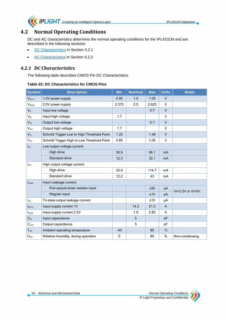
Creating an Intelligent Optical Layer IPL4101M Datasheet
54 Electrical and Mechanical Data Normal Operating Conditions
IP Light Proprietary and Confidential
4.2 Normal Operating Conditions
DC and AC characteristics determine the normal operating conditions for the IPL4101M and are described in the following sections:
DC Characteristics in Section 4.2.1
AC Characteristics in Section 4.2.2
4.2.1 DC Characteristics
The following table describes CMOS Pin DC Characteristics.
Table 22: DC Characteristics for CMOS Pins
Symbol Description Min Nominal Max Units Notes
VDD10 1.0V power supply 0.95 1.0 1.05 V
VDD25 2.5V power supply 2.375 2.5 2.625 V
VIL Input low voltage 0.7 V
VIH Input high voltage 1.7 V
VOL Output low voltage 0.7 V
VOH Output high voltage 1.7 V
VTL Schmitt Trigger Low to High Threshold Point 1.25 1.48 V
VTH Schmitt Trigger High to Low Threshold Point 0.85 1.06 V
IOL Low output voltage current:
High drive 36.9 96.1 mA
Standard drive 12.3 32.1 mA
IOH High output voltage current:
High drive 32.6 114.7 mA
Standard drive 12.2 43 mA
ILEAK Input Leakage current:
Pull-up/pull-down resistor input ±90 μA VI=2.5V or VI=0V
Regular input ±10 μA
IOZ Tri-state output leakage current ±10 μA
IDD10 Input supply current 1V 14.2 21.5 A
IDD25 Input supply current 2.5V 1.9 2.85 A
CIN Input capacitance 5 pF
COUT Output capacitance 5 pF
TOP Ambient operating temperature -40 85 °C
HOP Relative Humidity, during operation 5 85 % Non-condensing.

Creating an Intelligent Optical Layer IPL4101M Datasheet
55 Electrical and Mechanical Data High Speed Differential IO Characteristics
IP Light Proprietary and Confidential
4.2.2 AC Characteristics
The following table describes CMOS Pin AC Characteristics.
Table 23: AC Characteristics for CMOS Pins
Symbol Description Min Nominal Max Units Notes
TRISE Output rise time 0.6 1.1 ns 10% to 90% of full output swing with load capacitance of 10pF.
TFALL Output fall time 0.6 1.1 ns 90% to 10% of full output swing with load capacitance of 10pF.
TSETUP Setup time 1 ns Related to input signal and its sampling clock (unless otherwise specified).
THOLD Hold time 1 ns Related to input signal and its sampling clock (unless otherwise specified).
4.3 High Speed Differential IO Characteristics
The following table describes the high speed differential IO parameters.
Table 24: High Speed Differential IO Parameters
Parameter Min Nominal Max Units
Differential Input Resistance 85 100 115
Differential Input Data Level 20 2500 mVpp
Differential Output Resistance 85 100 115
Differential Output Data Level (LVCML/LVPECL) 200 1200 mVpp
Differential Output Rise time (10% to 90%) 30 ps
Differential Output Fall time (90% to 10%) 30 ps
Differential Skew 5 ps
NOTE—Differential output levels depend on output amplitude and pre-emphasis configurations.
4.4 EOI Characteristics
The following table describes the EOI timing characteristics.
Table 25: EOI Timing Characteristics
Symbol Description Min Nominal Max Units
TCID Delay from clock to OHCID 2.5 ns
TCRXOH Delay from clock to RxOH Data 2.5 ns
TCOHVAL Delay from clock to receive overhead valid 2.5 ns
TCREQ Delay from clock to transmit OH data request 2.5 ns
TTXSETUP TxOH Data setup time 2.5 ns
TTXHOLD TxOH Data hold time 2.5 ns
TCMFAS Delay from clock to transmit OH MFAS 2.5 ns
FEOIREF EOI reference clock frequency 64 80 MHz
Duty cycle EOI reference clock duty cycle 40 60 %
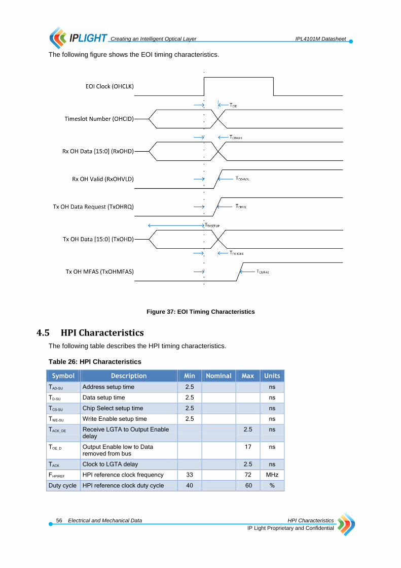
Creating an Intelligent Optical Layer IPL4101M Datasheet
56 Electrical and Mechanical Data HPI Characteristics
IP Light Proprietary and Confidential
The following figure shows the EOI timing characteristics.
Figure 37: EOI Timing Characteristics
4.5 HPI Characteristics
The following table describes the HPI timing characteristics.
Table 26: HPI Characteristics
Symbol Description Min Nominal Max Units
TAD-SU Address setup time 2.5 ns
TD-SU Data setup time 2.5 ns
TCS-SU Chip Select setup time 2.5 ns
TWE-SU Write Enable setup time 2.5 ns
TACK_OE Receive LGTA to Output Enable delay
2.5 ns
TOE_D Output Enable low to Data removed from bus
17 ns
TACK Clock to LGTA delay 2.5 ns
FHPIREF HPI reference clock frequency 33 72 MHz
Duty cycle HPI reference clock duty cycle 40 60 %
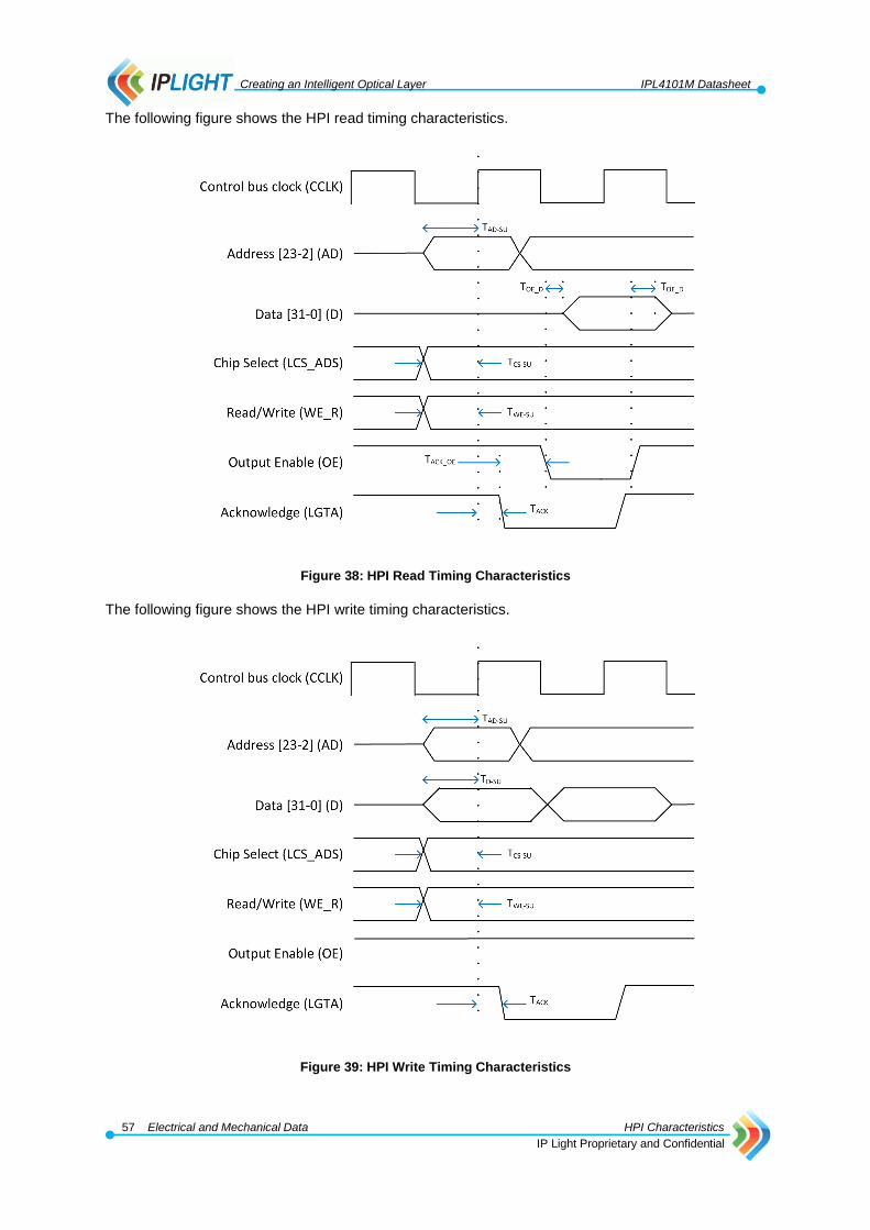
Creating an Intelligent Optical Layer IPL4101M Datasheet
57 Electrical and Mechanical Data HPI Characteristics
IP Light Proprietary and Confidential
The following figure shows the HPI read timing characteristics.
Figure 38: HPI Read Timing Characteristics
The following figure shows the HPI write timing characteristics.
Figure 39: HPI Write Timing Characteristics
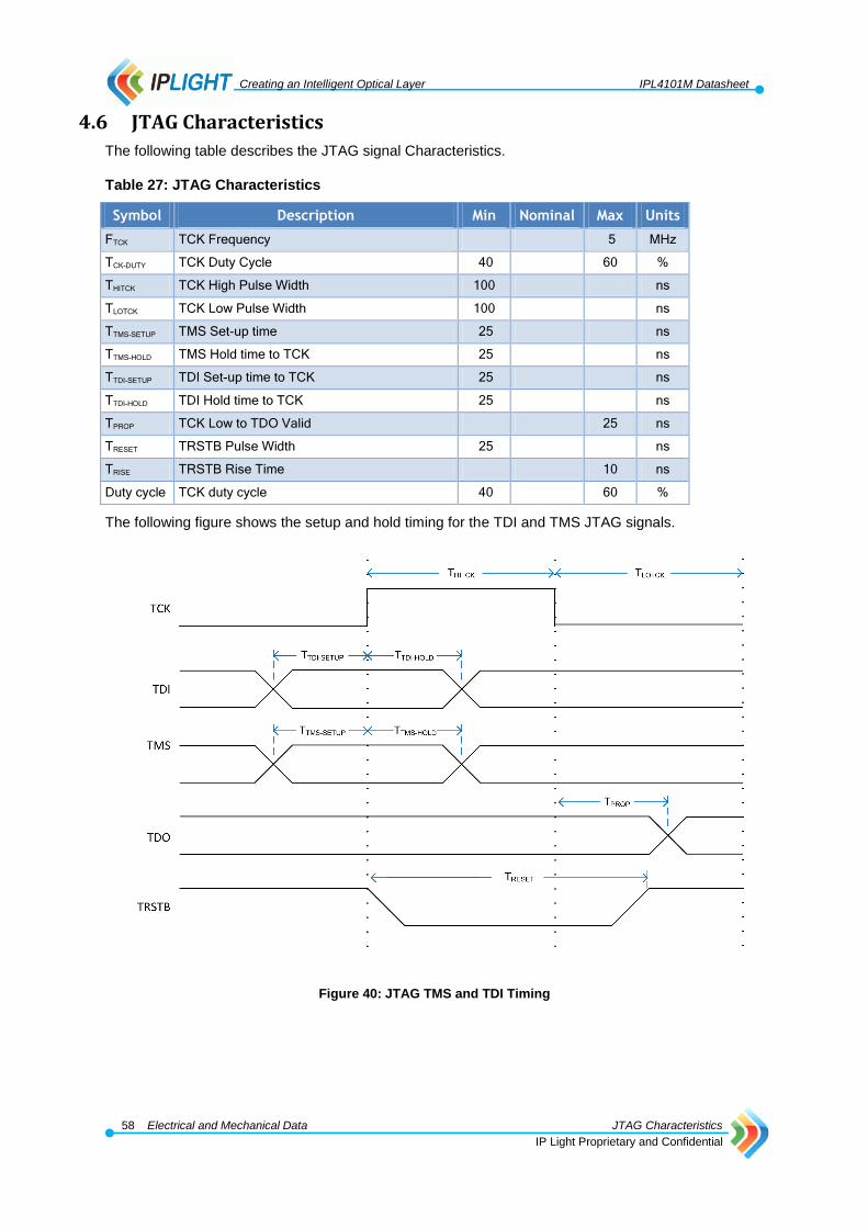
Creating an Intelligent Optical Layer IPL4101M Datasheet
58 Electrical and Mechanical Data JTAG Characteristics
IP Light Proprietary and Confidential
4.6 JTAG Characteristics
The following table describes the JTAG signal Characteristics.
Table 27: JTAG Characteristics
Symbol Description Min Nominal Max Units
FTCK TCK Frequency 5 MHz
TCK-DUTY TCK Duty Cycle 40 60 %
THITCK TCK High Pulse Width 100 ns
TLOTCK TCK Low Pulse Width 100 ns
TTMS-SETUP TMS Set-up time 25 ns
TTMS-HOLD TMS Hold time to TCK 25 ns
TTDI-SETUP TDI Set-up time to TCK 25 ns
TTDI-HOLD TDI Hold time to TCK 25 ns
TPROP TCK Low to TDO Valid 25 ns
TRESET TRSTB Pulse Width 25 ns
TRISE TRSTB Rise Time 10 ns
Duty cycle TCK duty cycle 40 60 %
The following figure shows the setup and hold timing for the TDI and TMS JTAG signals.
Figure 40: JTAG TMS and TDI Timing

Creating an Intelligent Optical Layer IPL4101M Datasheet
59 Electrical and Mechanical Data Clock Parameters
IP Light Proprietary and Confidential
4.7 Clock Parameters
The output reference clock rate is calculated differently for high and low rate output clocks as follows:
High rate output clock—the configured reference clock divided by 64 for high rate references and by 16 for low rate references
Low rate output clock—the configured reference clock divided by 64 for High rate references and by 16 for Low rate references and further divided by a configurable even value between 2 and 131072
The following table describes the input reference clock parameters.
Table 28: Input Reference Clock Parameters
Parameter Name Min Nominal Max Units
REFCLK Frequency 155.52 MHz
REFCLK Differential swing 300 1200 mV
REFCLK Duty Cycle 45 55 %
REFCLK Accuracy -20 +20 ppm
REFCLK Input Jitter (12 KHz - 20 MHz BW) 155.52 MHz 0.7 ps
REFCLK Input Random Jitter 2.6 ps-rms
The following table describes the output reference clock tolerances.
Table 29: Output Reference Clock Tolerances
Parameter Name Min Nominal Max Units
High-rate clock frequency 155.52 200 MHz
Low-rate clock frequency 1 100000 KHz
High-rate clock duty cycle 48 50 52 %
Low-rate clock duty cycle 48 50 52 %
4.8 Reset Signal Parameters
The following table describes parameters for the reset signal.
Table 30: Reset Parameters
Parameter Name Description Min Nominal Max Units
TRST_N RST_N pulse width 100 ns
The following figure shows reset signal timing.
Figure 41: RST_N Timing
After the device is powered up, you must allow 1 ms before applying RST_N.

Creating an Intelligent Optical Layer IPL4101M Datasheet
60 Electrical and Mechanical Data Thermal Information
IP Light Proprietary and Confidential
4.9 Thermal Information
NOTE—The values presented here are preliminary estimates.
The following table describes thermal resistance values.
Table 31: Thermal Resistance
Thermal Resistance Value
Junction to Ambient, JA 10.8° C/W for still air
7.6° C/W for 1m/s air flow
6.9° C/W for 2m/s air flow
Junction to Board, JB 4.0° C/W
Junction to Case, JC 0.2° C/W
It is recommended to use a heat sink to maintain normal operating conditions for the device. For more
information about the operating conditions, see Normal Operating Conditions in Section 4.2.
4.10 Power
The IPL4101M provides flexible operational modes, and therefore typical power dissipation can vary widely. The following table describes typical power utilizations for a variety of configurations.
Table 32: Typical Power Dissipation
Application Power
Dissipation Configuration
20G longhaul gateway 4.8W Two serial client OTU2 interfaces with FEC to two serial network OTU2 interfaces with EFEC.
20G, one OTU2 ring, ODU0/1 add/drop granularity
6.9W Two network OTU2 serial interfaces (one East side and one West side) to four client GbE (GFP-T) and one client OC-48/STM-16 interfaces. One ODU1 signal pass through between East and West.
10G framer 3.5W Single client OTU2 or OC-192/STM-64 or 10GE or FC-1200 interface to a single OTU2 network interface with EFEC.
10G muxponder 5.5W One OTU2 network interface with EFEC to four client GbE and two client OC-48/STM16 interfaces.
The IPL4101M provides configuration dependent power optimization. Logic blocks and IPLightSERDES™ lanes can be powered off when not being used. For example, if one NSP is configured for serial OTU2, then only one lane is used, and the three other unused lanes can be shutdown. Similarly, when configured to XBI2-2, only two lanes are used, and two must be shutdown.
Power Up/Down Sequences
WARNING—You must adhere to the following power up/down sequences carefully to avoid causing damage to the device.
To power up the IPL4101M:
1. Connect the ground supply. 2. Connect the power supply. 3. Connect the IO signals.
To power down the IPL4101M:
1. Disconnect the IO signals. 2. Disconnect the power supply. 3. Disconnect the ground supply.

Creating an Intelligent Optical Layer IPL4101M Datasheet
61 Ordering Information
IP Light Proprietary and Confidential
5 Ordering Information The materials of the IPL4101M are compliant with RoHS requirements.
The following table describes the Apodis I part number details to use when ordering the IPL4101M.
Table 33: Part Number
Part Number Description
IPL4101M-10 896 pin high performance flip-chip BGA
RoHS5
IPL4101M-20 896 pin high performance flip-chip BGA
RoHS compliant (RoHS6)
For information about availability and pricing, please contact your local IP Light distributor.
Creating an Intelligent Optical Layer IPL4101M Datasheet
62 Glossary
IP Light Proprietary and Confidential
Glossary
The glossary contains acronyms and terms specific to the Apodis I family of optical transport network processors.
Table 34: Glossary of Terms
Term Description
ALM ALarM
AMP Asynchronous Mapping Procedure
APS Automatic Protection Switching
CBR Constant Bit Rate
CMOS Complementary Metal Oxide Semiconductor
CSP Client Signal Processor
DCC Digital Communication Channel
EFEC Enhanced FEC
EOI External Overhead Interface
FAS Frame Alignment Signal
FC Fibre Channel
FE Fast Ethernet
FEC Forward Error Correction
GbE GigaBit Ethernet
GCC General Communication Channel
GE Gigabit Ethernet
GFC Gigabit Fibre Channel
GFEC Generic FEC
GFP Generic Framing Procedure
GFP-F Generic Framing Procedure—Frame mapped
GFP-T Generic Framing Procedure—Transparent
GMP Generic Mapping Procedure
HPI Host Processor Interface
IEEE the Institute of Electrical and Electronics Engineers, incorporated
IPG Inter-Packet Gap
IRQ Interrupt ReQuest
ITU-T International Telecommunication Union-Telecommunication standardization sector
JTAG Joint Test Action Group
LOL Loss Of Lock
LOS Loss Of Signal
LSB Least Significant Bit
MFAS Multi-Frame Alignment Signal
MLD Multiple Lane Distribution
MSA MultiSource Agreement
NSP Network Signal Processor
OAM/OA&M Operations, Administration and Maintenance

Creating an Intelligent Optical Layer IPL4101M Datasheet
63 Glossary
IP Light Proprietary and Confidential
Term Description
OC-n Optical Carrier of a synchronous transport module
ODU Optical channel Data Unit
OH OverHead
OHCID OH Channel IDentification
OPU Optical channel Payload Unit
OTN Optical Transport Network
OTU Optical channel Transport Unit
PLL Phase-Locked Loop
PM Performance Monitoring
PRBS Pseudo-Random Binary Sequence
PT Payload Type
RMON Remote network MONitoring
RMS Root Mean Square
SDH Synchronous Digital Hierarchy
SerDes Serializer/Deserializer
SFP Small Form-factor Pluggable
SONET Synchronous Optical NETwork
STM-n Synchronous Transport Module
TAF Transparent Agnostic Fabric
TCM Tandem Connection Monitoring
TDI Test Data Input
TMS Test Mode Selection
XAUI 10 Gb Attachment Unit Interface
XBI2 high speed (10Gbps) Backplane Interface for OTU2/ODU2
XFI 10 Gb small Form-factor pluggable module Interface
XGMII 10 Gb Media Independent Interface

Creating an Intelligent Optical Layer IPL4101M Datasheet
64 Reader Comments
IP Light Proprietary and Confidential
Reader Comments
In an on going effort to produce more effective documentation, the documentation staff at IP Light Ltd. welcomes any comments regarding this manual. Please use this form to communicate suggestions for improving this publication, or to inform us of any needed corrections.
Thank you for your assistance.
Apodis I IPL4101M IPL4101M Datasheet Version 1.01 April 2013
Comment Page Number
Name: _____________________________________________ Date: ________________________
Company: __________________________________________ Phone: _______________________
Address: ___________________________________________ Fax: _________________________
____________________________________________ Email: _______________________
Mail to: Technical Documentation Group Attention: Joshua Gold Phone: +972-3-721-1810 IP Light Ltd. 4 Hashiloach Street Fax: +972-3-921-5076 PO Box 7209 Petach Tikva 49250 Israel Email: [email protected]

IP Light Ltd.
4 Hashiloach Street PO Box 7209
Petach Tikva 49250 Israel
Phone: +972-3-721-1810 Fax: +972-3-921-5076
Email: [email protected] Web Site: http://www.iplight.com