ap211841 cambridge azur 840c cd player service manual
TRANSCRIPT

Gallery Court Hankey Place London SE1 4BB UK Tel: +44 (0)20 7940 2200 Fax: +44 (0)20 7940 2233
840CIssue Date: 07th February 2007
SERVICE MANUAL
SPECIFICATIONS:
D/A Converters Dual Analog Devices Total correlated jitter <130pS
AD1955 24 bit DAC’s
Crosstalk @1kHz <-130dB
Digital Filter Analog Devices Black Fin Crosstalk @20kHz <-114dB
ADSP-BF532 32 bit DSP
Performing ATF™ Output impedance <50 ohms
Up sampling to 24 bit 384 kHz
Digital input word
widths supported 16-24 bit
Analog Filter 2 Pole Fully Differential
Linear Phase Bessel Filter Digital output word
widths supported 16, 20, 24 bit
Frequency Response 20Hz – 20kHz (+\-0.1dB) Digital input sampling 32kHz, 44.1kHz,48kHz,88.2kHz
frequencies supported 96kHz, 176.4kHz, 192kHz
THD @ 1 KHz 0dBFs <0.0005% Digital output sampling 32 kHz – 192 kHz pass through
frequencies supported (including 44.1 kHz for CD)
48 kHz, 96 kHz, 192 kHz up sampled
THD @ 1Khz -10dBFs <0.0004% Audio output up sampling Fixed 24 bit, 384kHz
THD @ 20 KHz 0dBFs <0.0007% Dimensions (H x W x D) 115 x 430 x 360 mm
(4.5 x 16.9 x 14.7”)
IMD (19/20 kHz) 0dBFs <0.0002%
Weight 8.5kg (18.7lbs)
Linearity @ -90dBFs +/- 0.5dB
Stopband Rejection > 120dB
(>24 kHz)
S to N ration, A weighted >113dB
AP21184/1
1

840C SERVICE MANUAL
TABLE OF CONTENTS
Safety Precautions & Important Notes 3
Laser Safety Precautions 4
Exploded Diagram 5
Exploded Diagram Parts List 6
Functional Block Diagram 7
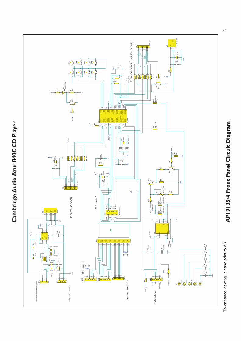
Front Panel Circuit Diagram 8
Front Panel PCB Layout (Top Side) 9
Front Panel PCB Layout (Bottom Side) 10
Front Panel PCB BOM 11
Servo Circuit Diagram (DAC) 12
Servo Circuit Diagram (Servo) 13
Servo PCB Layout (Top Side) 14
Servo PCB Layout (Bottom Side) 15
Servo PCB BOM 16-17
Voltage Select Switch Circuit Diagram 18
Voltage Select Switch PCB Layout (Top Side) 19
Voltage Select Switch PCB Layout (Bottom Side) 20
Voltage Select Switch PCB BOM 21
DAC DSP Circuit Diagram (Abus) 22
DAC Test Signals (Main Signal Paths General) 23
DAC DSP Circuit Diagram (DSP) 24
DAC Test Signals (Main Signal Paths General) 25
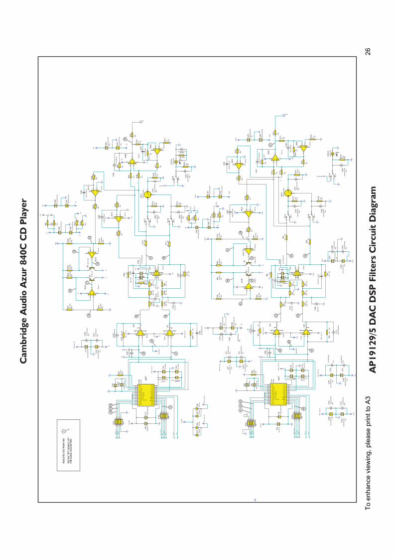
DAC DSP Circuit Diagram (Filters) 26
DAC Test Signals (Main Signal Paths Left Channel) 27-28
DAC Test Signals (Main Signal Paths Right Channel) 29-30
DAC DSP Circuit Diagram (Supply) 31
DAC DSP Circuit Diagram (Flash) 32
DAC DSP Board Layout (Top Side) 33
DAC DSP Board Layout (Bottom Side) 34
DAC DSP PCB BOM 35-37
Mains PCB Circuit Diagram 38
Mains PCB Board Layout (Top Side) 39
Mains PCB Board Layout (Bottom Side) 40
Mains PCB BOM 41
IC Pin Layout Details 42-50
Circuit Description 51
Software Instructions 52-61 2

SAFETY PRECAUTIONS & IMPORTANT NOTES
1. Check that the rear of the product indicates the correct supply voltage for
your area.
2. The lighting flash with the arrowhead within an equilateral
triangle is intended to alert the user or service agent to the
presence of dangerous voltages within the product enclosure that
may be of sufficient magnitude to constitute a risk of electric shock
to persons.
3. The exclamation point within an equilateral triangle is intended
to alert the user or service agent to the presence of important
operating and maintenance (Servicing) instructions in the literature
accompanying the appliance.
4. This product complies with EEC Low Voltage (73/23/EEC) and
Electromagnetic Compatibility (89/336/EEC) Directives when used and serviced
in accordance with this manual. For continued compliance all components
marked safety and EMC critical must only be replaced by Cambridge Audio
approved parts.
5. Any unauthorised design alterations or additions will void the manufacturer’s
warranty; furthermore the manufacturer cannot accept responsibility for personal
injury or property damage resulting therefrom.
6. When servicing, care should be taken to observe the original routing and
dressing of the leads and it should be confirmed that they have been returned to
normal after re-assembly.
Notes on chip component replacement
Never reuse a component that has been removed from a PCB
Notice that the minus side of a tantalum capacitor may be damaged by heat
COPYRIGHT NOTICE.
© 2007 Audio Partnership PLC. All rights reserved.
Cambridge Audio and Azur are registered trademarks for Audio Partnership PLC. This document
may not be reproduced, distributed, transmitted, displayed, published, or broadcast without the
express written prior permission of Audio Partnership PLC.
Alteration or removal of any trademark, copyright, or other notice from this content is prohibited.
Information provided in this document is provided solely for the use of official service agents in
repairing and servicing Audio Partnership PLC products.
3

LASER SAFETY PRECAUTIONS
Caution: These labels may be attached to the unit on the rear and inside toinform that it contains a laser component. Use of controls or adjustments, orperformance of procedures other than those specified within the service orinstruction manual may result in hazardous radiation exposure.
WARNING!
1. Service should only be performed by qualified personnel.
2. This equipment has been designed and manufactured to meetinternational safety standards; it is the legal responsibility of the repairer toensure that these safety standards are maintained.
3. Any repairs must be made in accordance with the relevant safetystandards.
4. It is essential that safety and EMC critical components are replaced withCambridge Azur approved parts only.
CLASS 1 LASER PRODUCT
NOTES ON HANDLING THE OPTICAL PICK-UP BLOCK OR BASE UNITThe laser diode in the optical pick-up block may suffer electrostatic breakdown because of thepotential difference generated by the charged electrostatic load, etc. on clothing and the humanbody.
During repair, pay attention to electrostatic breakdown and also use the procedure in the printedmatter which is included in the repair parts.The flexible board is easily damaged and should be handled with care.
NOTES ON LASER DIODE EMISSION CHECKThe laser beam on this model is concerated so as to be focused on the disc reflective surface bythe objective lens in the optical pick-up block. Therefore, when checking the laser diodeemission, observe from more than 30cm away from the objective lens.
4

Cam
bri
dge A
ud
io A
zu
r 840C
CD
Pla
yer
Exp
lod
ed
Dia
gra
mT
o e
nh
an
ce
vie
win
g,
ple
ase
prin
t to
A3
5

Cam
bri
dge A
ud
io A
zu
r 840C
CD
Pla
yer
Exp
lod
ed
Dia
gra
m P
art
s Lis
t
noitpircseD
ecn erefeR
yrotc aFt r a
PP
A.f e
Rgn i
warD
1PY
1228
7003
-008
010E
006
Scre
w M
3*8
M/C
1/K
Tor
x Re
cess
ZN
-PT
(Silv
er)
1PY
1229
7003
-008
010E
001
Scre
w M
3*8
M/C
1/K
Tor
x Re
cess
BLK
-PT
(Bla
ck)
2PY
1218
6574
-010
003E
000-
01A
zur 8
40C
Top
Pane
l (Bl
ack)
2PY
1219
6574
-010
003E
000-
02A
zur 8
40C
Top
Pane
l (Si
lver
)
3PY
1127
6574
-150
013E
000-
01A
zur 8
40A
Sid
e Pa
nel,
(Bla
ck)
3PY
1128
6574
-150
013E
000A
01A
zur 8
40A
Sid
e Pa
nel,
Silv
er
4PY
1110
4006
-840
058E
001
840C
DA
C M
odul
e
5PY
1217
3200
-080
551E
000
Tran
sfor
mer
AC1
15/2
30V
T080
55A
<AP1
9141
/4>A
zur-
840C
6PY
940
9692
-006
002-
201
Azu
r V2
CD M
echa
n as
sy w
ith S
anyo
DA
11V
Rev
A
Not
Sho
wn
PY94
130
09-1
1000
0-00
2V2
CD
San
yo L
aser
DA
11V
7PY
1220
8584
-001
010E
301
Azu
r 840
C U
K/EU
Bla
ck F
ront
Pan
el A
ssy
7PY
1221
8584
-001
000E
301
Azu
r 840
C U
K/EU
Silv
er F
ront
Pan
el A
ssy
8PY
1222
4006
-840
001E
000
Azu
r 840
C D
ispl
ay M
odul
e M
BCF0
0003
B00V
0 <R
CL>
9PY
1223
6574
-010
002E
000-
01A
zur 8
40C
Fron
t Pan
el -B
Art
wor
k (P
rint C
ool G
rey
7C) B
lack
9PY
1224
6574
-010
002E
000A
01A
zur 8
40C
Fron
t Pan
el-S
Art
wor
k (P
rint C
oll G
rey
8C) S
ilver
10PY
1225
9484
-001
000E
041
Azu
r-84
0C C
ontr
ol P
CB A
ssy
Rev
A
11PY
1226
9484
-001
000E
181
Azu
r-84
0C S
ervo
PCB
A <
T-TY
PE>
Rev
A
12PY
554
6564
-010
006-
000-
01A
zur 6
40C.
B CD
Doo
r W/S
ilksc
reen
PM
S Co
ol G
rey
7C
12PY
568
6564
-010
006-
000A
01A
zur 6
40C.
S CD
Doo
r W/S
ilksc
reen
PM
S Co
ol G
rey
7C
13PY
1122
6074
-150
004E
000
Azu
r 840
A P
last
ic F
oot (
Blac
k) A
P168
37*
13PY
1124
6074
-150
004E
000A
01A
zur 8
40A
Pla
stic
Foo
t (Si
lver
) AP1
6837
*
14PY
1165
9805
-084
000E
001
Azu
r 840
A/C
Rem
ote
Cont
rol A
ssy
Rev
A
Not
Sho
wn
PY12
2751
00-8
4010
0E10
0A
zur 8
40C
Mul
tilin
gual
Use
r Man
ual (
AP1
8655
*)
Expl
oded
Dra
win
g Pa
rts
List
6

Cam
bri
dge A
ud
io A
zu
r 840C
CD
Pla
yer
Fu
nct
ion
al B
lock
Dia
gra
m
DSP
DC
SERV
OCI
RCU
ITCU
RREN
TSO
URC
ECI
RCU
IT
ITO
V
ITO
VD
IFFE
REN
TIA
LFI
LTER
/AM
P
DIF
FERE
NTI
AL
TOSI
NG
LEEN
DED
UN
BALA
NCE
DO
/P
BALA
NCE
DO
/PD
AC
WD
CLK
BITC
LK
SDA
TAL
RESE
T
MU
TEDA
CCO
NTR
OL
I/F
DA
C1M
CLK
24.5
76M
Hz
CLO
CK+
BUFF
ER
SPD
IFTX
CLK
SPD
IFRX
MCL
K
DA
C2M
CLK
DA
C1M
CLK
DSP
CLK
WD
CLK
BITC
LK
SDA
TAL
SPD
IFRX
SET
UP
I/F WD
CLK
BITC
LK
SDA
TAL
(SPD
IFSU
BCO
DE
DA
TA)
SPD
IFTX
SET
UP
I/F
AU
DIO
DA
TALE
FT
FLA
SHM
EMO
RY
SPD
IFRE
CEIV
ER
TRA
NSM
ITTE
R
AU
DIO
DA
TAL&
R
SPD
IF
FLA
SHA
DD
RESS
&D
ATA
SPD
IFTO
LOG
ICLE
VEL
SPD
IFTO
LOG
ICLE
VEL
SPD
IFI/P
1
SPD
IFI/P
2
SPD
IFI/P
SWIT
CHIN
GO
PTIC
AL
COA
X
COA
X
OPT
ICA
L
LOG
ICTO
SPD
IFLE
VEL
SPD
IFO
/PCO
AXOPT
ICA
L44
.1 k
Hz
PASS
THRO
'SET
TIN
G
44.1
/48/
96/1
92kH
z
44.1
kHz
FRO
MCD
SERV
O
PASS
THRO
'SET
TIN
G
48/9
6/19
2kH
zU
P/D
OW
NSA
MPL
ED
CDSE
RVO
TOM
ECH
CON
NEC
TIO
NS
DC
SERV
OCI
RCU
ITCU
RREN
TSO
URC
ECI
RCU
IT
ITO
V
ITO
VD
IFFE
REN
TIA
LFI
LTER
/AM
P
DIF
FERE
NTI
AL
TOSI
NG
LEEN
DED
UN
BALA
NCE
DO
/P
BALA
NCE
DO
/PD
AC
WD
CLK
BITC
LK
SDA
TAL
RESE
T
MU
TE
DA
CSE
TU
PI/F
DA
C2M
CLK
DA
CPC
B
MEC
HA
ND
SERV
OPC
B
BC P
OVRESH
CEM
SPD
IFI/P
SWIT
CHIN
G
CDSE
RVO
TOLC
DCO
NN
ECTI
ON
S
PSU
MIC
ROCO
NTR
OLL
ER/D
SPIN
TERF
ACE
MIC
ROTO
LCD
(DO
TM
ATR
IX)
MIC
ROCO
NTR
OLE
R(P
IC)
RS23
2
IRU
NM
OD
I/P O/P
I/PIR
MO
D
DRA
WER
OPE
NCL
OSE
CO
NN
ECTI
ON
S
DRA
WER
OPE
NCL
OSE
CO
NN
ECTI
ON
S
LCD
DRA
WER
SPEE
DCO
NTR
OL
KEY
COM
MA
ND
STO
SERV
O(D
IGIT
AL
POT
FOR
RES
LAD
DER
I/P)
DIG
ITA
LPO
T
K1K2
I/P
FRO
NT
PAN
NEL
BUTT
ON
SM
ICRO
TOLC
D(D
OT
MA
TRIX
)
FRO
NT
PAN
ELIR
MO
DI/P
IRM
OD
FRO
MRE
MO
TE
SPD
IFI/P
SWIT
CHIN
GCO
NTR
OL
DSP
CLK
AU
DIO
DA
TAL&
R
SPD
IFTX
CLK
SPD
IFRX
MCL
K
RS23
2(L
OG
ICLE
VELS
)
MO
DU
LATE
DIR
LEFT
CH
RIG
HT
CH
RESE
T
UBI
T
RESE
T
(SPD
IFSU
BCO
DE
DA
TA)
CBI
T(S
PDIF
SUBC
OD
ED
ATA
)
UBI
T
X1U
15
U4
CN3
U5
CN4
U10
CN5
U23
U23 U
6
U7
U9
44.1
kHz
FRO
MCD
SERV
O
44.1
kHz
FRO
MCD
SERV
O
U8
FRO
NT
PAN
ELPC
B
U11
U12
U13
U19
U20
U32
U13
0
U13
1
U33
U34U
38
U37
U39
U40
U41
U52
Q7
Q9
CN12CN
13 CN14
U35
U50
U46
U53
Q3
Q5
U1
RELA
Y
MU
TECI
RCU
ITA
UD
IOO
/PRL
1RL
2RL
3Q
2Q
4Q
8
OEI
(PIC
MU
TE)
U3
2U
5U
4U
U28
U1
U2
U3
Q1
AU
DIO
DA
TALE
FT
To
en
ha
nce
vie
win
g,
ple
ase
prin
t to
A3
7
Cam
bri
dge A
ud
io A
zu
r 840C
CD
Pla
yer
AP
19135/4
Fro
nt
Pan
el C
ircu
it D
iagra
m
CON
TRO
LBU
S
SPID
ATA
RXSP
IIN
TSP
IDA
TATX
SPIC
LKSP
ICS
SERI
AL
TXSE
RIA
LRX
OE1
SO1_
U7SO
2_U
7SO
1_U
9M
UTE
C1 1n50
VX7
R
C2 1n50
VX7
R
1 2 3 4 5 6 7
CN1
CON
N-H
7
K1 K2PO
WER
DET
ECT
RESE
T
GN
D+5
VRE
MO
TE
1 2 3 4 5 6 7 8
CN2
CON
N-H
8
1 2 3 4 5 6 7 8
CN3
CON
N-H
8
1 2 3 4 5 6 7
CN4
CON
N-H
7
+5V
+5V
3
OPT
1
GN
D2
U1
TSO
P18
IRRE
CEIV
ERC3 10
0n
R1 47R
SW1
Stan
dby
SW2
Men
u
SW6
Stop
SW3
Sele
ct
SW4
Ope
n/Cl
ose
SW5
Play
/Pau
se
SW7
Back
Skip
SW8
Forw
ard
Skip
R2 220R
LED
MCL
R/VP
P1
RA0/
AN0
2
RA1/
AN1
3
RA2/
AN2
4
RA3/
AN3/
VREF
5
RA4/
T0CK
I6
RA5/
AN4/
SS7
RE0/
RD/A
N5
8
RE1/
WR/
AN6
9
RB4
37RB
3/PG
M36
RB2
35
RB0/
INT
33VD
D32
VSS
31RD
7/PS
P730
RD6/
PSP6
29
RB1
34
RD5/
PSP5
28RD
4/PS
P427
RC7/
RX/D
T26
RC5/
SDO
24RC
4/SD
I/SD
A23
RD3/
PSP3
22RD
2/PS
P221
RC6/
TX/C
K25
VDD
11
VSS
12
OSC
1/CL
KIN
13
OSC
2/CL
KOU
T14
RCO
/T1O
SO/T
1CKI
15
RC1/
T1O
SI/C
CP2
16
RC2/
CCP1
17
RC3/
SCK/
SCL
18
RD0/
PSP0
19
RE2/
CS/A
N7
10
RD1/
PSP1
20
RB5
38
RB6/
PGC
39
RB7/
PGD
40
U2
PIC1
6F87
4A
+5V
R3 56R
R4 56R
C4 100n
F
X1CR
YSTA
L
FREQ
=20
MH
z
C5
22pF
C6
22pF
C7 10U
16V
R5 100R
C8 100n
F
R6 10K
+5V
Vss
Vdd
VoRS
R/W
ED
0D
1D
2D
3D
4D
5D
6D
7
LED
ALE
DK
C9 100n
F
+5V
SERV
ORE
SET
IRO
UT
C10
100n
F
+5V
LED
SERV
ORE
SET
ToSe
rvo
Boar
d
LCD
Conn
ecto
r2
LCD
Conn
ecto
r1
From
Serv
oBo
ard
(LCD
)
+5V
R9 220R
C11
10U
16V
RESE
T
RESE
T
+5V
LCD
C12
100n
F
ON
/OFF
BRIG
HT
BRIG
HT
ON
/OFF
Q1
BC33
7
R12
10K
Q2
BC33
7R1
3
10K
Q3
BC33
7
Q4
BC33
7
R14
1K2
R15
10K
H0
14
A16
GN
D8
A07
W0
12
L13
L013
H1
1
W1
4
A25
SDA
10
SCL
9VC
C16
U3
DS1
803
+5V
_SER
VO
+5V
_SER
VO
123456789
CN6
JST
2MM
S9B-
PH-K
S
1 2 3 4 5 6 7 8
CN7
JST
2MM
S8B-
PH-K
S
R18
10K
R19
10K
SEG
1516
SEG
1415
SEG
1314
SEG
1213
SEG
1112
SEG
1011
SEG
910
SEG
89
SEG
78
SEG
67
SEG
56
SEG
45
SEG
34
SEG
23
SEG
12
SEG
01
SEG
1617
SEG
1718
SEG
1819
COM
120
COM
221
COM
322
COM
423
NC
24
CN10
LCD
740C
COM
1
COM
1CO
M2
COM
3CO
M4
COM
2CO
M3
COM
4
+5V
R20
100R
R21
100R
R22
100R
R23
100R
R24
100R
R25
100R
R26
100R
R27
100R
R28
100R
R29
100R
R30
100R
R31
100R
R32
100R
CLK
SDTX
SDRX
CS INT RS
E
OSC
1O
SC2
U7_
SO1
U7_
S02
U9_
S01
SCL
D4 D
5D
6D
7SD
A
SERI
AL
TXSE
RIA
LRX
SERV
ORE
SET
RESE
TO
E1#
MU
TE
IR O
UT
IRIN
D1
LED
3MM
BLU
E
C13
10U
16V
C14
100n
F
1
P1 PAD
EMC
M3
1
P2 PAD
EMC
M3
1
P3 PAD
EMC
M3
C15
1nF
C16
1nF
C17
1nF
R10
300R
1 3
2
R11
PRE
MU
LTI5
00R
MCL
R4
GP4
3CL
KIN
2Vs
s8
GP0
7G
P16
GP2
5
Vdd
1U
4
PIC1
2C50
8
1 2 3 4 5
CN8
DA
TA
1 2 3 4 5
CN9
DA
TA
R33
680R
R34
680R D2
BZX79C5V1500MW
D3BZX79C5V1500MW
MG
ND
+5V
_SER
VO
MG
ND
FIN
1
GN
D1
2
RIN
3
GN
D2
5
VCC
6
OU
T27
COM
8
OU
T19
U5
BA62
18
MG
ND
+8V
1 2 3 4 5 6
1a 2a 3a 4a 5a 6a7 8
7a 8a
CN5
CON
N-8
HEA
DD
UA
LBO
T
D4
1N4004
D51N4004 C18
10U16V
C19
100n
F
+8V
R35
100K
LED
1
P4 PAD
EMC
M3
1
P5 PAD
EMC
M3
C20
1nF
C21
1nF
C22
100n
F
TOD
AC
BOA
RDCN
8(S
PI)
TOD
AC
BOA
RDCN
9 (R
S232
/MU
TE/S
PDIF
CNTR
L)
FRO
MSE
RVO
BOA
RDD
RAW
ERO
PEN
/CLO
SE(S
PI)
TOM
ECH
DRA
WER
OPE
N/C
LOSE
(SPI
)
R7 100R
R8 10O
R
R16
RM
ETA
L1/
8W4k
71/
8WM
etal
Film
R17
RM
ETA
L1/
8W4k
71/
8WM
etal
Film
R36
RM
ETA
L1/
4W22
0R1/
4WM
etal
Film
R37
RM
ETA
L1/
4W22
0R1/
4WM
etal
Film
D6
1N40
04D
71N
4004
To
en
ha
nce
vie
win
g,
ple
ase
prin
t to
A3
8

Cam
bri
dge A
ud
io A
zu
r 840C
CD
Pla
yer
AP
19135/3
Fro
nt
Pan
el B
oard
Layo
ut
(To
p S
ide)
To
en
ha
nce
vie
win
g,
ple
ase
prin
t to
A3
9

Cam
bri
dge A
ud
io A
zu
r 840C
CD
Pla
yer
AP
19135/3
Fro
nt
Pan
el B
oard
Layo
ut
(Bo
tto
m S
ide)
To
en
ha
nce
vie
win
g,
ple
ase
prin
t to
A3
10

AP19138/5AP Part
No.Value Description Factory Part No Qty Component Ident Notes
47R 0.25 W 1% Metal Fil m 1 R156R 0.25 W 1% Metal Fil m 2 R3, R4100R 0.25 W 1% Metal Fil m 16 R5, R7, R8, R20-R3 2220R 0.25 W 1% Metal Fil m 1012-201014E000 4 R2, R9, R36, R3 7300R 0.25 W 1% Metal Fil m 1 R10680R 0.125 W 1% Metal Fil m 1016-801016E020 2 R33, R341K2 0.25 W 1% Metal Fil m 1 R144K7 0.25 W 1% Metal Fil m 2 R16, R1 710k 0.25 W 1% Metal Fil m 6 R6, R12, R13, R15,R18, R1 9100K 0.25 W 1% Metal Fil m 1 R35
PRE MULTI 500R Side adjust Footprint 9.5 x 4.5 mm
VR B500 OHM +-10% WI 3296NOXOX-XA1-013
1 R11Mount on bottom side of PCB with screw adjust facing upwards
22p 6C,5C2mm0.5=hctiP,OPNcimareCF12C,02C,71C-51C,2C,1C7mm0.5=hctiPV05cimareCFn1
9mm0.5=hctiPV05cimareCFn001C3, C4, C8-C10, C12, C14, C19, C22
10uFMiniature 16V Pitch 2.5mm Height 5.2mm
4 C7, C11, C13, C18
1U1REVIECERRIPOSTV3SS6381POSTMount 13.5mm height from PCB, Please support using foam pad spacer
2U1CIPP/I-A778F61CIPProgramme with AP20058/2, Please add version label - See AP Service Dept.
PY983 DS18030-050 DIGITAL PO T 4118-030051E200 1 U3
4U1CIPP/I-A805C21CIPProgramme with AP20231/1, Please add version label - See AP Service Dept
PY260 BA6218 5U1CIREVIRDDC
PY214 BC33 7 NPN SMALL SIGNA L 4 Q1-Q4
1D1EULBDEL5V1 ZENE R BZX79C5V1 1402-511201E20 0 2 D2, D3
7D,6D,5D,4D4REIFITCERESOPRUPLARENEG4004N1
PY043 TACT SWITCHTACT SW 2P2T KPT-1105A (5MM)
8 SW1-SW8
MPP03-+1X1SU94-CHFP02LCMM5.3TUOBATHGIEH,zHM02LATSYRCzHM02
MISCELLANEOUS
Cambridge Audio Azur 840C Front Panel PCB BOM
RESISTORS
CAPACITORS
SEMICONDUCTORS
TRANSISTORS
DIODES
Note: resistors, capacitors and other 'generic' electronic components arenot usually stocked by the manufacturer. Please obtain these locally.
11

Cam
bri
dge A
ud
io A
zu
r 840C
CD
Pla
yer
AP
18432/3
CD
Serv
o P
CB
Sch
em
ati
c (D
AC
)
SDAT
A1
DEM
/SCL
2
LRCK
3
MCL
K4
AOU
TL8
VA+
7
AGN
D6
AOU
TR5
U5
CS43
33/3
8
C41
0.1u
F
C40
10uF
25V
C39
10uF
25V
C32
10uF
25V
R75
15K
R82
15K
R80
12K
R74
12K
C42 39
0pF
C38
390p
F
3 21
8 4
U4:
A NJM
2100
5 67
U4:
B
NJM
2100
R73
47K
C33 10
pF
C34
10uF
25V
1 2 3
CN9
GN
D
R71
56K
C43
10uF
25V
R70
56K
C35
0.1u
F
+5V
L.CH
R.CH
+8V
R81
47K
C36 10
pF
R79
20K
R72
20K
C37
220u
F16
V1 2 3
CN10
GN
DL.
CH
R.CH
GN
D
1 2 3 4 5
CN13 DIG
DA
TA
12CN
14
MCL
K
R68
100R
R69
100R
34 5
RL1:
B
1 2
RL1:
A
678
RL1:
C
R83
120R
0.5W
R88
1K
14.5
V
Q3
8050
Q4
8050
C55
47uF
16V
R89
330k D
1
IN41
48R9
039
0R
D7
IN40
04
R87
100R
Q6 90
12
R85
560RR8
6
3K9
C63
4.7u
F16
V
D6
IN40
04
12345CN
11
GN
DRO
UT
LOU
T
MU
TE1
MU
TE
AC
R84
4K7
Q5
9012
C88
1nF
D12
1N40
01
To
en
ha
nce
vie
win
g,
ple
ase
prin
t to
A3
12

Cam
bri
dge A
ud
io A
zu
r 840C
CD
Pla
yer
AP
18432/3
CD
Serv
o P
CB
Sch
em
ati
c (S
erv
o)
SEG1477
SEG1576
SEG1675
SEG1774
SEG1873
NC72
NC71
NC70
NC69
NC68
NC67
NC66
NC65
NC64
NC63
NC62
NC61
NC60
NC59
NC58
NC57
NC56
NC55
NC54
NC53
FL/TL52
VDD51
SEG1378
SEG1279
SEG1180
SEG1
081
SEG9
82
SEG8
83
SEG7
84
SEG6
85
SEG5
86
SEG4
87
SEG3
88
SEG2
89
SEG1
90
SEG0
91
COM
392
COM
293
COM
194
COM
095
VLC
96
NC97
NC98
NC99
VDD
100
VSS
50
(BO
OT)
49
VARE
F48
ADK1
47
ADK2
46
ADK3
45
PWR
DET
44
NC43
NC42
OLT
41
CLT
40
SLT
39
D-O
PEN
38
D-CL
OSE
37
BUS3
36
BUS2
35
BUS1
34
BUS0
33
BUCK
32
CEE
31
VSSS1
XOUT2
XIN3
RESET4
NC5
NC6
TEST7
NC8
REMOTE9
MUTE10
NC11
NC12
NC13
SCK214
(SI2)15
(SO2)16
(WAIT)17
NC18
NC19
NC20
NC21
NC22
NC23
NC24
NC25
NC26
NC27
NC28
CORW29
RES30
U3 TOSH
CDM
CU
1 2 3 4 5 6 7
CN6
LCD
1 2 3 4 5 6 7 8
CN5
LCD
1 2 3 4 5 6 7 8
CN4
LCD
R22
NC R21
22K
+5V
C83
470u
F16
V
C85
100u
F16
V
+5V
+5VD
D
C84
220u
F16
V
Q13
9014
C
X2 CRYS
TAL
7.37
28M
Hz
C81
25pF
C80
25pF
C79
100n
FR1
9
3K3
R18
10K
D9 1N41
48
R20
1K
1 2 3 4 5 6 7 8
CN3
PROG
RAM
MIN
G
R65
10K
R66
2K2
R17
10K
+5V
R27
10K
+5V
+5VD
D
XVSS77
VDD476
PXO75
PXI74
VSS473
TESIO172
TESIN71
DACT70
CKSE69
DMOUT68
IO367
IO266
IO165
IO064
VSS363
VDD362
FLGD61
FLGC60
FLGB59
FLGA58
SEL57
2VREF56
DMO55
TEBC254
TEBC153
TEBC052 RFGC51
XI78
XO79
XVDD80
DVSR
81
RO82
DVDD
83
DVR
84
LO85
DVSL
86
TEST
187
TEST
288
TEST
389
BUS0
90
BUS1
91
BUS2
92
BUS3
93
VDD
94
VSS
95
BUCK
96
CCE
97
TEST
498
TSM
OD
99
RST
100
VREF
50
TRO
49
FOO
48
TEZI
47
TEI
46
TSIN
45
SBAD
44
FEI
43
RFRP
42
RFZI
41
RFCT
40
AVDD
139
RFI
38
SLCO
37
AVSS
136
VCO
F35
VCO
REF
34
PVRE
F33
LPFO
32
LPFN
31
TEST01
HSO2
UHSO3
EMPH4
LRCK5
VSS16
BCK7
AOUT8
DOUT9
MBOV10
IPF11
SBOK12
CLCK13
VDD114
VSS215
DATA16
SFSY17
SBSY18
SPCK18
SPDA20
COFS21
MONIT22
VDD223
TESIO024
P2VREF25
HSSW26
ZDET27
PDO28
TMAXS29TMAX30
U2
TC94
62F
VCC
1RF
GC2
GMAD
3FN
I4
FPI
5
TNI
7M
DI8
LDO
9SE
L10
TEB
112V
RO12
TEN
13TE
O14
SBAD
15FE
O16
FEN
17
SEB
18
VRO
19
RFRP
20
BTC
21
RFCT
22
PKC
23
RFRP
IN24
RFGO
25
GVSW
26
AGCI
N27
RFO
28
GND
29
RFN2
30
TPI
6
U1 TA21
53FN
PWGN
D1
OUT
(-)1
2
PVCC
13
OUT
(+)1
4
VIN1
5
VRI
6
VCI
7
VIN2
8
OUT
(+)2
9
PVCC
210
OUT
(-)2
11
PWGN
D12
PWGN
D13
OUT
(-)3
14PV
CC3
15O
UT(+
)316
VIN3
17S
GND
18S
VCC
19VI
N420
OUT
(+)4
21PV
CC4
22O
UT(-)
423
PWGN
D24
U6 TA20
92N
R1510K
R39
10K
R1410K
R1310K
R1210K
+5V
R1110K
R6 220K
R768K
R515K
R947K
C80.
015u
FC7
647
pF
C7447uF16V
R810K
C750.01uF
C60.0027uF
1 2 3
CN1
DIGI
TAL
OUT
+5V
R10
47R
C11
0.04
7uF
C10
47uF
16V
C9 47uF
16V
12345678910111213141516CN
16
MEC
H
123456CN
15
MOT
ORDR
IVE
+8V
C56
220u
F16
V
C59
100n
F
R64
10K
+5V
C58
100n
F
C57
100n
F
R42
3K3
C27
0.04
7uF
C26
0.04
7uF R4
13K
3
C60
0.04
7uF
C61
100n
F
C1422uF16V
C2847uF16V
R38
R37R4
010
R1/
4W NC NC NC NC NC
R36
R35
X1CR
YSTA
L16
.934
4MHz
C17
15pF
C16
15pF
C15
0.04
7uF
NC
C19
0.04
7uF
C1847uF16V
NCNCNCNCNCNCNC
NC
NCNCNC
NC
R43 10
KR4
53K
3
C24
470p
F
C25
470p
F
R44
3K3
C62
100n
F
R60
1K
R59
82K
L147
uH
C66
0.04
7uF
C65
220u
F16
V
C20
47uF
16V
C67
100n
F
C64
100n
F
C68
22uF
R58
0R
R56
10K
R55
10K
R54
10K
R53
10K
R52
56K
R51
47K
R50
47K
R49
47K
R48
47K
R57
56KL2 10
uH
Q1 9015
R62
15R
C69
100u
F16
V
R46
3K3
R47
3K3
C23
0.04
7uF
C220.047uF
R63
100K
R1 2K2
C1 3pF
R3 1KC73
100p
F
R2 10K
R422
0R
C210
0nF
C72
0.22
uF
C30.
22uF
C410
0nFR6
127
K
C71
100n
F
C7
0.01
uFC5 0.
047u
F
C77
47uF
16V
C78
47uF
16V
C70
47uF
16V
NC
D8 1N41
48
NCNC
NCNCNCNCNC
NCNCNCNC
NCNCNC
C13
0.04
7uF
C12
1uF
16V
C29
47uF
16V
R16
10K
12345CN
8
DRAW
DRIV
E
R31
10K
R30
10K
+5V
Q12 8050
Q7 8050Q9 85
50Q
10 8550
R33
470R
R34
470R
R67
14m
mlin
k(84
0con
ly)
+8V
R28
10K
R29
10K
+5V
+5V
NCNC
NCNCNCNCNCNCNCNCNCNCNCNCNCNCNCNCNCNCNCNC
NC NC NC
NCNC
NC
C86
100n
FL3 10
0uH
R2610K
R251K
R2310K
R2410K
R32
4K7
REM
OTE
REM
OTE
LK1
LINK
OPEN
=F/
LSH
ORT
=T/
L
+5VC
C
NCNCNC
NCNCNCNCNCNCNCNCNCNCNC
12345CN
12
12345CN
2
DATA
OUT
EMPHBC
KPC
MD
LRCKGN
D
1 2
CN17
XTAL
I
OSC
GND
SETLCDCONTRAST
+5V
RESE
TBO
OT GND
WAI
TSC
K2 SI2
SO2
REM
OTE
+5V
GND
K1 K2
C21
0.00
47uF
OLT
GND
CLT
OPEN
CLOS
E
GND
ROUT
LOUT
MUT
E1M
UTE
+5V
GND
D-OU
T
FC-
TR-
TR+
FC+
PD VR LD GND
F C B A D E VCC
VCSLT-
SLT+
FM+
FM-
DM-
DM+
SEG1
8SE
G17
SEG1
6SE
G15
SEG1
4SE
G13
SEG1
2
SEG1
1SE
G10
SEG9
SEG8
SEG7
SEG6
SEG5
SEG4
SEG3
SEG2
SEG1
SEG0
COM
0CO
M1
COM
2CO
M3
L410
0uH
L5 100u
H
C82
10uF
16V
1 2
CN18
XTAL
O
GND
C87
1nF
1 2
CN20
MUT
E
1234567CN
7
CONT
ROL
KEYS
D10
1N41
48
D11
1N41
48
R76 4K
7
Q8 8050
Q11
8050
PWR
DET
RESE
T
J1 100R
FU1
T2AL
VI1
VO3
GND 2
U8 7805
C45
100n
FC4
410
0nF
C46
470u
F16
V
+5V
1 2
CN19 AC
IN
D5IN
4004
D4IN
4004
D2IN
4004
D3IN
4004
C49
100n
F
C50
3300
uF25
V
C54 10
0nF
VI1
VO3
GND 2
U7 7808
C48
100n
FC5
3 100n
F
C51
100n
F
C52
100n
F
C47
470u
F16
V
+8V
14.5
V
AC
1 2
CN21
FPDI
S
NOFITFOR740/840C
To
en
ha
nce
vie
win
g,
ple
ase
prin
t to
A3
13

Cam
bri
dge A
ud
io A
zu
r 840C
CD
Pla
yer
AP
12927/8
CD
Serv
o B
oard
Layo
ut
(To
p S
ide)
To
en
ha
nce
vie
win
g,
ple
ase
prin
t to
A3
14

Cam
bri
dge A
ud
io A
zu
r 840C
CD
Pla
yer
AP
12927/8
CD
Serv
o B
oard
Layo
ut
(Bo
tto
m S
ide)
To
en
ha
nce
vie
win
g,
ple
ase
prin
t to
A3
15

AP19969/3AP Part
NoValue Description Qty Component Ident Factory Part no Notes
000-410000-110104R1rotsiseRmliFlateMW52.0R0115R 0.125 W Metal Film Resistor 1 R62
knilesU.YLNOC048roF76R1knilmm41knil000-810007-4101,01R1rotsiseRmliFlateMW521.0R74
100R 0.125 W Metal Film Resistor 1 wirelink ( J1 ) 1011-001016-000wirelink is positioned between C68 and L2. This must be 100R resistor
000-810102-21014R1rotsiseRmliFlateMW521.0R022000-610107-410143,33R2rotsiseRmliFlateMW521.0R074
1K 0.125 W Metal Film Resistor 5 R3, 20, 25, 60 1011-002018-000000-610202-210166,1R2rotsiseRmliFlateMW521.02K2
3K3 0.125 W Metal Film Resistor 7 R19, 41, 42, 44, 45, 46, 47 1013-302018-000000-610207-410167,23R2rotsiseRmliFlateMW521.07K4
10K 0.125 W Metal Film Resistor 26R2, 8, 11, 12, 13, 14, 15, 16, 17, 18, 26, 27, 28, 29, 30, 31, 39, 43, 53, 54, 55, 56, 64, 65
1011-003016-000
000-810305-1101,5R1rotsiseRmliFlateMW521.0K5122K 0.125 W Metal Film Resistor 1 R2127K 0.125 W Metal Film Resistor 1 R6147K 0.125 W Metal Film Resistor 5 R9, 48, 49, 50, 51 1014-703016-00056K 0.125 W Metal Film Resistor 2 R52, 57
000-810308-6101,7R2rotsiseRmliFlateMW521.0K8682K 0.125 W Metal Film Resistor 1 R59 1018-203018-000100K 0.125 W Metal Film Resistor 1 R63 1011-004016-000220K 0.125 W Metal Film Resistor 1 R6 1012-204016-000
3pF Ceramic COG 50V 5mm Pitch 1 C115pF Ceramic COG 50V 5mm Pitch 2 C16, 17 1100-150043-00025pF Ceramic COG 50V 5mm Pitch 2 C80, 81 1100-250042-00047pF Ceramic COG 50V 5mm Pitch 1 C76 1100-470043-000100pF Ceramic COG 50V 5mm Pitch 1 C73470pF Ceramic 50V 5mm Pitch 2 C24, 25 1100-471043-000
000-340201-001178C1hctiPmm5V05cimareCFn110nF Ceramic 50V 5mm Pitch 1 C75 1100-103043-00010nF Mylar 5mm Pitch 1 C715nF Ceramic 50V 5mm Pitch 1 C8 1100-153043-000
47nF Ceramic 50V 5mm Pitch 11C5, 11, 13, 15, 19, 22, 23, 26, 27, 60, 66
1100-473044-000
100nF Ceramic 50V 5mm Pitch 20C2, 4, 44, 45, 48, 49, 51, 52, 53, 54, 57, 58, 59, 61, 62, 64, 67, 71, 79, 86
1106-104044-000
220nF Ceramic 50V 5mm Pitch 2 C3, 72 1100-224044-000000-360272-10116C1hctiPmm5ralyM7n2000-260274-101112C1hctiPmm5ralyM7n4
1uF 16V Electrolytic 1 C12 1102-107044-00010uF 16V Electrolytic 1 C82 1102-100024-00022uF 16V Electrolytic 2 C14, 68 1102-220014-000
47uF 16V Electrolytic 10C9, 10, 18, 20, 28, 29, 70, 74, 77, 78
1102-470014-000
100uF 16V Electrolytic 2 C69, 85 1102-101014-000220uF 16V Electrolytic 3 C56, 65, 84 1102-221014-000470uF 16V Electrolytic 3 C46, 47, 83 1102-471014-0003300uF 25V Electrolytic 1 C50 1102-332024-000
PY474 TA2153FN TOSHIBA RF Amplifier 1 U1 4121-530103-000
PY475 TC9462FGTOSHIBA Digital Servo-chip Processor
ABIHSOTPFQSNIP001000-321026-49142U1
Cambridge Audio Azur 840C Servo PCB Assembly BOM
RESISTORS
CAPACITORS
SEMICONDUCTORS
Note: resistors, capacitors and other 'generic' electronic components arenot usually stocked by the manufacturer. Please obtain these locally.
16

AP19969/3AP Part
NoValue Description Qty Component Ident Factory Part no Notes
Cambridge Audio Azur 840C Servo PCB Assembly BOM
PY565 TOSHCDMCUMCU TMP87EP26F-1J15 SOP TOSHIBA
000-301062-78143U1
000-350029-02146U1CIrevirdrewoPABIHSOTN2902AT374YPfit heatsink to top of driver IC
006-203080-87147U1rotalugeRV8+022-OT8087613YPmount on heatsing using heatsink comound only
007-433050-87148U1rotalugeRV5+022-OT5087530DPPY014 C8050D NPN Transistor TO92 4 Q7, 8, 11, 12 1300-805000-100PY558 9014C NPN Transistor 1 Q13 1300-901400-100
001-000558-103101,9Q2rotsisnarTPNP0558C955YP001-005109-10311Q1rotsisnarTPNPC5109065YP
1N4148 Signal Diode 3 D9, 10, 11 1401-141480-0001N4004 Rectifier Diode 4 D2, 3, 4, 5 1401-140040-000 stand up off PCB by 7.5mm
000-343961-00611X1hctiPmm5niP2zHM4439.61720YP099-282737-00612X1hctiPmm5niP2zHM8273.7165YP
100-000200-00321271NC2TSJhctiPmm2yaW2100-000300-0032,1NC1TSJhctiPmm2yaW3000-000500-0032,8,2NC2TSJhctiPmm2yaW5000-000600-003251NC1TSJhctiPmm2yaW6000-000700-00327,6NC2TSJhctiPmm2yaW7000-000800-00325,4,3NC3TSJhctiPmm2yaW8300-001200-003291NC1TSJhctiPmm5.2yaW2000-109610-103261NC1hctiPmm0.1CFFyaW61
100-001050-13041UF1redloHesuFtnuoMBCPmm02
T2AL2A delay 20mm Fuse 250V LBC (low breaking capacity)
100-200816-03041UF1
10uH Inductor 8mm Pitch 1 L2
001-003074-40511L1hctiPmm8rotcudnIHu74
001-003101-40515,4,3L3hctiPmm8rotcudnIHu001
CRYSTALS
CONNECTORS
MISCELLANEOUS
Note: resistors, capacitors and other 'generic' electronic components arenot usually stocked by the manufacturer. Please obtain these locally.
17

Cam
bri
dge A
ud
io A
zu
r 840C
CD
Pla
yer
AP
17977/2
Vo
ltage S
ele
ct S
wit
ch P
CB
Sch
em
ati
c
J2 FRO
MJ4
(Com
mon
)
SW1
VOLT
SELE
CTRF
1002
B11
5/23
0VM
arki
ng
J1 BRO
WN
(230
V)
J3 BLA
CK(1
15V)
To
en
ha
nce
vie
win
g,
ple
ase
prin
t to
A3
18

Cam
bri
dge A
ud
io A
zu
r 840C
CD
Pla
yer
AP
17977/2
Vo
ltage S
ele
ct S
wit
ch B
oard
Layo
ut
(To
p S
ide)
To
en
ha
nce
vie
win
g,
ple
ase
prin
t to
A3
19

Cam
bri
dge A
ud
io A
zu
r 840C
CD
Pla
yer
AP
17977/2
Vo
ltage S
ele
ct S
wit
ch B
oard
Layo
ut
(Bo
tto
m S
ide)
To
en
ha
nce
vie
win
g,
ple
ase
prin
t to
A3
20

AP17980/1AP Part
NoValue Description Qty Component Ident Factory Part Number Notes
000-002010-60421WS1rotceleSegatloVB2001FR
Cambridge Audio Azur 840C V2 Voltage Selector PCB Assembly BOM
CONNECTORS
Note: resistors, capacitors and other 'generic' electronic components arenot usually stocked by the manufacturer. Please obtain these locally.
21

Cam
bri
dge A
ud
io A
zu
r 840C
C
D P
layer
AP
19129/4
DA
C D
SP
Cir
cuit
Dia
gra
m (
AB
us)
IRO
UTIR
IN
IRIN
CN10
0JA
CK-C
KX-3
.5-1
2
3.5m
m JA
CK
+5V3
OPT1
GND2
U1 TSO
P183
6 IR
RECE
IVER
+5V
123
U3:A
4011
VDD
=+5V
VSS=
GND
1 2
6 5 4NC
3
U2 OP4
N25
5 64
U3:B
4011
VDD
=+5V
VSS=
GND
8 910
U3:C
4011
VDD
=+5V
VSS=
GND
12 1311
U3:D
4011
VDD
=+5V
VSS=
GND
+5V
C3 10uF
16V
36kH
z
IRreceiver
A K
D1
CAIR
DEM
ODU
LATO
R
12
5 CN1:
AAV
2-8,
4-14
/EC
34
5
CN1:
BAV
2-8,
4-14
/EC
R1 220R
0805
R3 10K
0805
R4 10K
0805
Q1
BC81
7-16
SM
R5 10K
0805
R6 100R
0805
R7 100R
0805
R8 2R2
0805
C11N
50V
NP0
SM
0805
IRO
UT
R9 47R
0805
need
to a
ssig
n pa
ckag
e
123456789
CN2
CONN
-9W
D-T
YPE
+5V
SERI
AL_R
X
SERI
AL_T
X
RS23
2
R15 100R0805
C5 1N50
VNP
0SM
0805
C6 1N50
VNP
0SM
0805
OUT
PUT
1GN
D2
VCC
3
U4 APRX
179A
T
12
3
CN3
AV-8
,4-8
ES
C7 100N50VY5VSM0805
C8 10U
16V
EL
R16
100R
0805
C111N50VNPOSM0805
R18
75R
0805
OUT
PUT
1GN
D2
VCC
3
U5 APRX
179A
T
12
3
CN4
AV-8
,4-8
ES
C9 100N50VY5VSM0805
C10
10U
16V
EL
R17
100R
0805
C131N50VNPOSM0805
R19
75R
0805
12
U6:A
74VH
C14
VCC=
+5V_
DIG
56
U6:C
74VH
C14
VCC=
+5V_
DIG
1312U6
:D 74VH
C14
VCC=
+5V_
DIG
1110
U6:E
74VH
C14
VCC=
+5V_
DIG
98
U6:F
74VH
C14
VCC=
+5V_
DIG
R20
100R
0805
R21
10K
0805
R22
100R
0805
R23
10K
0805
R24
100R
0805
R25
100R
0805
C17
100P50VY5VSM0805
C18
100P50VY5VSM0805
MULTIPLEXER1 MULTIPLEXER2
1E1
S12
1-IN
33
1-IN
24
1-IN
15
1-IN
06
2-IN
313
2-IN
212
2-IN
111
2-IN
010
GND
8
2E15
SO14
1Y7
2Y9
VCC
16
U7 74VH
C153
3.3V
SO1_
U7
3.3V
C19
100N
50V
Y5V
SM08
05
R26
10K
0805
R27
10K
0805
1 23
U8:A
74VH
C32
VCC=
3.3V
4 56
U8:B
VCC=
3.3V
10 98
U8:C
VCC=
3.3V
13 1211
U8:D
VCC=
3.3V
R28
0R08
05
CS84
16_R
XP0
MULTIPLEXER 1 MULTIPLEXER 2
1E1
S12
1-IN
33
1-IN
24
1-IN
15
1-IN
06
2-IN
313
2-IN
212
2-IN
111
2-IN
010
GND
8
2E15
SO14
1Y7
2Y9
VCC
16
U9
CS84
06_T
XP
+5V_
DIG
C20
100N
50V
Y5V
SM08
05
SO1_
U9SO
2_U9
fs =
44.1
kHz
fs=
48kH
zmin
serv
o sp
difp
ass t
hrou
gh
fs =
44.1
kHz
spdi
f inp
ut p
ass t
hrou
gh
R29
1K 0805
R31
430R
0805
R32
91R
0805
12
3
CN5
AV-8
,4-8
ES
C22
100P50VY5VSM0805
C23100N50VY5VSM0805
GND
1
VCC
2
INPU
T3
U10
APTX
179A
T
+5V_
DIG
+5V_
DIG
+5V_
DIG
C24 100N50VY5VSM0805
C26
10U
16V
EL
R33
100R
0805
74HC
T153
12
U23:
A
VCC=
+5V_
DIG
34
U23:
B
VCC=
+5V_
DIG
56
U23:
C
VCC=
+5V_
DIG
1312
U23:
D
VCC=
+5V_
DIG
1110
U23:
E
VCC=
+5V_
DIG
98
U23:
F
VCC=
+5V_
DIG
34
U6:B
74VH
C14
VCC=
+5V_
DIG
R65
1K 0805
+5V
T1
R1
+5V
T1
R1
400K
400K
5K 5K
C1+
1
C1-
3
C2+
4
C2-
5
T2IN
10
R1O
UT12
T1IN
11T1
OUT
14
T2O
UT7
R1IN
13
R2O
UT9
R2IN
8
V-6
V+2
VCC16
GND15
U28
MAX
202
SM
C144
100N
50V
X7R
SM08
05
C145
100N
50V
X7R
SM08
05
C146
100N
50V
X7R
SM08
05C1
4710
0N50
VX7
RSM
0805
C148
100N
50V
X7R
SM08
05
R70
100R
0805
R71
100R
0805
C161
100N
50V
Y5V
SM08
05
+5V_
DIG
C162
100N
50V
Y5V
SM08
05
+5V_
DIG
C163
100N
50V
Y5V
SM08
05
3.3V
L2 47UH
SM
L3 47UH
SM L4 47UH
SM
74HC
U04
C12
100N
50V
X7R
SM08
05
C14
100N
50V
X7R
SM08
05
C21
100N
50V
X7R
SM08
05
C210
0N50
VX7
RSM
0805
C410
0N50
VX7
RSM 08
05
SERV
O_S
PDIF
_OUT
R66
100R
0805
SERV
O_S
PDIF
_OUT
_3.3
V
C201
47P50VY5VSM0805
C202
47P50VY5VSM0805
C215
100N
50V
Y5V
SM08
05
C222
100N
50V
Y5V
SM08
05
R85
100R
0805
C275
100N
50V
X7R
SM08
05
C278
100N
50V
CER
C279
100N
50V
CER
R10
220R
0805
C273
posit
ion
100R
0805
C274
posit
ion
100R
0805
1
2
3
4
5
6
7
89
1IN
DICA
TES
TEST
POIN
TRE
F
SEE
DAC
TEST
SIGN
ALS
LIST
FOR
SIGN
ALDE
SCRI
PTIO
N
10
1112
To
en
ha
nce
vie
win
g,
ple
ase
prin
t to
A3
22

Cam
bri
dge A
ud
io A
zu
r 840C
CD
Pla
yer
AP
19129/5
DA
CTest
Sig
nals
(M
ain
Sig
nal P
ath
s G
en
era
l)
Test
Poi
nt
Sche
mat
ic R
efPa
geSi
gnal
Type
Mea
sure
men
tN
ode
tnemerusae
Mnoitpircse
DM
eter
Type
epocs‘langis
atadlairessuounitno
CV5
P/I1lacitp o
FIDPS
3ni p
7U
l atig iD
11
epocs‘langis
atadlairessuounitno
CV5
trevnocle velr et fa
P/I1
xao cFI
DPS31
nip7
Ul atig i
D1
2
epocs‘langis
atadlairessuou nitno
CV5
P/I2lacit po
FIDPS
4nip
7U
la ti g iD
13
epocs‘langis
atadlairessuounitno
CV5
tre vnoclevelretfa
P/I2
xao cFI
D PS21
nip7
Ulatig i
D1
4
epocs‘langis
atadlairessuoun itno
C3V3
)detceles2
ro1
P/I(2
ro1
P /I lacitp oFI
DPS1
nip8
Ula tig i
D1
5
epocs‘langis
atadlairessuounitno
C3V3
)detceles2
ro1
P/I(2
r o1
P/Ixaoc
FIDPS
2nip
8U
latig iD
16
epocs‘langis
atadla ire ss uounitno
C3V 3
)PSD
ot(0
hcXR
FIDPS
otno itce le s
P/Ire tfal angis
FIDPS
3nip
9U
latig iD
17
epocs‘langis
atadlai ressuounitno
CV5
)detceleskcaby a lp
DC(
ovresD
Cm orfla ngis
FIDPS
4ni p
8U
latigiD
18
ep ocs ‘l angis
atad lairessuoun itn o
C3V3
)PSD
ot(2
hcXR
FIDP S
oto vres
DC
m orflangisFI
DPS6
ni p8
Ulatig i
D1
9 101
Dig
ital
U9
pin
5SP
DIF
sig
nal f
rom
CD
ser
vo 3
V3 p
ass
thro
’ (CD
pla
ybac
k &
Pas
s th
ro’ s
elec
ted)
3V3
Cont
inuo
us s
eria
l dat
a si
gnal
‘sco
pe epocs‘langis
atadl air essuou nitno
C3 V3
)P SD
morf(X
TFI
DPSmorfla ngis
FIDPS
4ni p
9U
la tigiD
111
epocs‘langi s
atad lairessuounitno
CV 5
P/Ol acitpo/xao c
FIDPS
7nip
9U
latig iD
121
23

Cam
bri
dge A
ud
io A
zu
r 840C
C
D P
layer
AP
19129/4
DA
C D
SP
Cir
cuit
Dia
gra
m (
DS
P)
BITC
LKW
DCL
KSD
ATA
_LSD
ATA
_RCS
_DA
C1CS
_DA
C2
RELA
Y
SSD
SPRE
SET
RESE
TD
AC1
_MCL
KD
AC2
_MCL
KM
OSI
SCK
SS_1SCK_1DSP_MISO_1DSP_MOSI_1
D7
D6
D5
D4
D3
D2
D1
D0
A18
A17
A16
A15
A14
A13
A12A11A10A9A8A7A6A5
A4A3A2A1
WE_FLASH#
OE_FLASH#
CS_FLASH#
MU
TE
I2SDATAI2SFRAME
INTR
EQ
MIS
O
RXP3
1
RXP2
2
RXP1
3
RXP0
4
RXN
5
VA6
AG
ND
7
FILT
ER8
RST
9
RXP4
10
RXP5
11
RXP6
12
RXP7
13
AD
0/CS
14A
D1/
CDIN
15SC
L/CC
LK16
SDA
/CD
OU
T17
AD
2/G
PO2
18G
PO2
19G
PO0
20VL
21D
GN
D22
VD23
RMCK
24O
MCK
25SD
OU
T26
OSC
LK27
OLR
CK28
U11
CS84
16
CS84
16_R
XP0
SERV
O_S
PDIF
_OU
T_3.
3V
C27 100N50VY5VSM0805
3.3V
R34
1K08
05
C31
10U
16V
EL
1 2 3 45678
R35
100R
24.5
76M
Hz
3.3V
R37
10K
0805
R39
10K
0805
CS84
06_T
XP
R41 10
K08
05
VCC8
CLK5
N/C1
GND4
X1 24.5
76M
Hz
C36
10U
16V
EL
+5V_
OSC
12
U15
:A
74VH
C14
VCC=
OSC
_3.3
V
34U
15:B
74VH
C14
56U
15:C
74VH
C14
1312U
15:D
74VH
C14
1110U
15:E
74VH
C14
98U
15:F
74VH
C14
R42
100R
0805
R43
100R
0805
R44
100R
0805
R45
100R
0805
C37 10P50VY5VSM0805
C38 10P50VY5VSM0805
C39 10P50VY5VSM0805
C40 10P50VY5VSM0805
SCH
MIT
T IN
VERT
ER
C41 10P50VY5VSM0805
R46
100R
0805
12345 6 7 8
R49
33R
12345
678
R54
33R
R57
1K08
05
R58
1K08
05
12345
678
R55
33R
R56
10K
0805
R61
100R
0805
12345
678
R62
100R
12345 6 7 8
R36
33R
12345
678
R50
100R
1357
2468
9101113
1214
CN6
CON
N-7
HEA
DD
UA
L
1 2 3 45678
R51
10K
R524K70805
3.3V
DSP
JTEG
1.2V
3.3V
12345
678
R53
33R
12345
678
R59
33R
SDA
/CD
OO
UT
1
AD
0/CS
2
AD
23
RXP
4
TEST
5
VD6
TEST
7
TEST
8
RST
9
TEST
10
TEST
11
ILRC
K12
ISCL
K13
SDIN
14TC
BL15
TEST
16TE
ST17
TEST
18IN
T19
U20
OM
CK21
GN
D22
VL23
H/S
24TX
N25
TXP
26A
D1/
CDIN
27SC
L/CC
LK28
U12
CS84
06
3.3V
3.3V
R38 10
0R08
05
R40
100R
0805
12345
678
R60
100R
1 2 3 45678
R63
100R
23
1
U19
:A74VH
C125
VCC=
3.3V
56
4
U19
:B
VCC=
3.3V
98
10
U19
:C
VCC=
3.3V
1211
13
U19
:D
VCC=
3.3V
23
1
U20
:AVC
C=+5
V
56
4
U20
:B
74H
CT12
5
VCC=
+5V
98
10
U20
:CVC
C=+5
V
1211
13
U20
:DVC
C=+5
V
U_I
NTR
EQ
U_M
ISO
U_M
OSI
U_S
CLK
U_S
SU
_RES
ET
VCC
3RS
T2
GND 1
U21
DS1
818
1FU
NCT
ION
AL0
MO
DE
1BO
OT
0M
OD
E
GN
D1
GN
D2
GN
D7
VRO
UT2
4
VRO
UT1
5
VDD
EXT
6
GN
D8
GN
D9
CLKI
N10
XTA
L11
VDD
EXT
12
RESE
T13
NM
I14
GN
D15
RTXO
16
RTXI
17
VDD
RTC
18
GN
D19
VDD
EXT
20
PPI_
CLK
21
PPI0
22
PPI1
23
PPI2
24
PPI3
26VD
DIN
T25
PF15
/PPI
427
PF14
/PPI
528
PF13
/PPI
629
GN
D30
VDD
EXT
31
PF12
/PPI
732
PF11
/PPI
833
PF10
/PPI
934
PF9/
PPI1
035
PF8/
PPI1
136
PF7/
SPIS
EL7/
PPI1
237
PF6/
SPIS
EL6/
PPI1
338
GN
D39
GN
D40
GN
D41
GN
D42
GN
D43
GN
D44
VDDEXT 45
PF5/SPISEL5/PPI14 46
PF4/SPISEL4/PPI15 47
PF3/SPISEL3/PPI_FS3 48
PF2/SPISEL2 49
PF1/SPISEL1/TMRCLK 50
PF0/SPISS 51
VDDINT 52
SCK 53
MISO 54
MOSI 55
GND 56
VDDEXT 57
DT1SEC 58
DT1PRI 59
TFS1 60
TSCLK1 61
DR1SEC 62
DR1PRI 63
RFS1 64
RCLK1 65
VDDINT 66
DT0SEC 67
DT0PRI 68
TFS0 69
GND 70
VDDEXT 71
TSCLK0 72
DR0SEC 73
DR0PRI 74
RFS0 75
RSCLK0 76
TMR2 77
TMR1 78
TMR0 79
VDDINT 80
TX 81
RX 82
EMU 83
TRST 84
TMS 85
TD1 86
TD0 87
GND 88GN
D89
GN
D90
GN
D91
GN
D92
VDD
EXT
93TC
K94
BMO
DE1
95BM
OD
E096
GN
D97
DA
TA15
98D
ATA
1499
DA
TA13
100
DA
TA12
101
DA
TA11
102
DA
TA10
103
DA
TA9
104
DA
TA8
105
GN
D10
6VD
DEX
T10
7D
ATA
710
8D
ATA
610
9D
ATA
511
0
DA
TA4
112
VDD
INT
111
DA
TA3
113
DA
TA2
114
DA
TA1
115
DA
TA0
116
GN
D11
7VD
DEX
T11
8BG
119
BGH
120
AD
DR1
912
1A
DD
R18
122
AD
DR1
712
3A
DD
R16
124
AD
DR1
512
5A
DD
R14
126
AD
DR1
312
7G
ND
128
GN
D12
9G
ND
130
GN
D13
1G
ND
132
GND133
VDDEXT134
ADDR12135
ADDR11136
ADDR10137
ADDR9138
ADDR8139
ADDR7140
ADDR6141
ADDR5142
VDDINT143
GND144
VDDEXT145
ADDR4146
ADDR3147
ADDR2148
ADDR1149
ABE1150
ABE0151
AWE152
ARE153
AOE154
GND155
VDDEXT156
VDDINT157
AMS3158
AMS2159
AMS1160
AMS0161
ARDY162
BR163
SA10164
SWE165
SCAS166
SRAS167
VDDINT168
CLKOUT169
GND170
VDDEXT171
SMS172
SCKE173
GND174
GND175
GND176
GN
D3
U13
AD
SP-B
F532
R30
0R08
05R6
40R
0805
I2SERR
I2SERR
C28
100N50VX7RSM0805
C29
100N50VX7RSM0805
C30 10N50VX7RSM0805
C32
100N50VX7RSM
0805
C33100N50VX7RSM
0805
C97
100N50VX7RSM
0805
C74
100N50VX7RSM0805
C165
10U
16V
EL
C166
10U16VEL
C16710U16VEL
C75
100N
50V
X7R
SM08
05
C76
100N
50V
X7R
SM08
05
C77
100N
50V
X7R
SM08
05
C78
100N
50V
X7R
SM08
05C9
610
0N50
VX7
RSM
0805
C79
100N
50V
X7R
SM 0805
C80100N50VX7RSM
0805
C81 100N50VX7RSM0805
C82100N50VX7RSM
0805
C83100N50VX7RSM
0805
C84100N50VX7RSM
0805
C85
100N
50V
X7R
SM08
05
C86
100N
50V
X7R
SM08
05
C95
100N
50V
X7R
SM08
05C87
100N
50V
X7R
SM08
05
C88
100N
50V
X7R
SM08
05
C89100N50VX7RSM
0805
C90100N50VX7RSM
0805
C91100N50VX7RSM
0805
C92 100N50VX7RSM0805
C93100N50VX7RSM
0805
C94100N50VX7RSM
0805
C168100N50VX7RSM
0805
C169100N50VX7RSM
0805
3.3V
+5V
R132
100R
0805
D15
BAS1
675
V0,
3A
D16
BAS1
675
V0,
3A
MU
TE_P
IC
R135
10K
0805
3.3V
DSP
C149
10U
35V
EL
C143
10U
35V
EL
R15333R0805
R13010K0805
3.3V
DSP
123CN
11
HEA
DER
3WA
Y
HW
/SW
1.2V
DSP
R87
10K
0805
R88
10K
0805
3.3V
3.3V
R2 0R12
06R8
9
0R12
06
1IN
DIC
ATE
STE
STPO
INT
REF
SEE
DA
CTE
STSI
GN
ALS
LIST
FOR
SIG
NA
LD
ESCR
IPTI
ON
1314
1516
17
1819
20
21
To
en
ha
nce
vie
win
g,
ple
ase
prin
t to
A3
24

Cam
bri
dge A
ud
io A
zu
r 840C
CD
Pla
yer
AP
19129/5
DA
CTest
Sig
nals
(M
ain
Sig
nal P
ath
s G
en
era
l)
Test
Poi
nt
Sche
mat
ic R
efPa
geSi
gnal
Type
Mea
sure
men
tN
ode
tnemerusae
Mnoitpircse
DM
eter
Type
epocs‘eva
werau qs
zH
M675.423V3
kcolcret sa
mXR
FIDPS
52nip
1 1U
l at ig iD
231 14
2D
igita
lU
11 p
in 2
6Fr
om S
PDIF
RX
Dig
ital a
udio
Dat
a (S
PDIF
I/P
or C
D W
ith d
isc
play
ing)
3V3
Cont
inuo
us s
eria
l dat
a si
gnal
‘sco
pe
152
Dig
ital
U11
pin
27
From
SPD
IF R
X D
igita
l aud
io B
it CL
K ( C
D s
elec
ted
With
dis
c pl
ayin
g)3V
3 sq
uare
wav
e 2.
8MH
z (fo
r 44.
1kH
z sa
mpl
e fr
eq fr
om C
D)
‘sco
pe
162
Dig
ital
U11
pin
28
From
SPD
IF R
X D
igita
l aud
io W
ord
CLK
( CD
sel
ecte
d W
ith d
isc
play
ing)
3V3
squa
re w
ave
44.1
kHz
(for
44.
1kH
z sa
mpl
e fr
eq fr
om C
D)
‘sco
pe epocs‘eva
werauqs
zH
M675.423V3
kcolcretsa
mX
TF I
D PS12
nip21
Ulatigi
D2
7 1 182
Dig
ital
U12
pin
14
To S
PDIF
TX
Dig
ital a
udio
Dat
a (S
PDIF
I/P
or C
D W
ith d
isc
play
ing)
3V3
Cont
inuo
us s
eria
l dat
a si
gnal
‘sco
pe
192
Dig
ital
U12
pin
13
To S
PDIF
TX
Dig
ital a
udio
Bit
CLK
(CD
sel
ecte
d W
ith d
isc
play
ing
&
Ups
ampl
e fr
eque
ncy
set t
o 48
kHz)
3V3
squa
re w
ave
3M
Hz
(for 4
8kH
z sa
mpl
e fr
eq fr
om D
SP)
‘sco
pe
202
Dig
ital
U12
pin
12
To S
PDIF
TX
Dig
ital a
udio
Wor
d CL
K ( C
D s
elec
ted
With
dis
c pl
ayin
g)3V
3 sq
uare
wav
e 48
kHz
(for 4
8kH
z sa
mpl
e fr
eq fr
om D
SP)
‘sco
pe epocs‘e va
werauq s
zH
M675.423 V3
kcolcretsa
MPS
D83
C/44Rlatigi
D2
12
To
en
ha
nce
vie
win
g,
ple
ase
prin
t to
A3
25
Cam
bri
dge A
ud
io A
zu
r 840C
CD
Pla
yer
AP
19129/5
DA
C D
SP
Filte
rs C
ircu
it D
iagra
m
MUT
E
RESE
T
MUT
E
RESE
T
DAC
1_M
CLK
SCK
CS_D
AC1
MO
SI
DAC
2_M
CLK
SCK
CS_D
AC2
MO
SI
WD
CLK
BITC
LKSD
ATA_
R
SDAT
A_L
BITC
LKW
DCL
K
DVDD1
LRCLK2
BCLK3
SDATA/EF_LDATA4
EF_RDATA5
DSD_SCLK6
DSD_LDATA7
DSD_RDATA8
DSD_PHASE9
AGND10
IOUTR+11
IOUTR-12
FILTR13
IREF14 AVDD 15FILTB 16IOUTL- 17IOUTL+ 18AGND 19ZEROR 20ZEROL 21MUTE 22PD/RST 23CDATA 24CLATCH 25CCLK 26MCLK 27DGND 28
U130
AD19
55
DAC
1_VA
_+5V
DVDD1
LRCLK2
BCLK3
SDATA/EF_LDATA4
EF_RDATA5
DSD_SCLK6
DSD_LDATA7
DSD_RDATA8
DSD_PHASE9
AGND10
IOUTR+11
IOUTR-12
FILTR13
IREF14 AVDD 15FILTB 16IOUTL- 17IOUTL+ 18AGND 19ZEROR 20ZEROL 21MUTE 22PD/RST 23CDATA 24CLATCH 25CCLK 26MCLK 27DGND 28
U131
AD19
55
C53 47N50VECHUSM
C54
10U
25V
NP
DAC
2_V
A_+5
V
C55
10U
25V
NP
C56
47N
50V
ECHU
SM
LEFT
RIGH
T
+5V_
DAC
C98
10U
NP35
V
C99
10U
NP35
V+5V_
DAC
C15347N50VECHUSM
C154
10U
25V
NP
C155 47N50VECHUSMC1
5610
U25
VNP
C151
10N
50V
ECHU
SM
C152
10U
25V
NP
C15747N50VECHUSM
C48
47N
50V
ECHU
SM
C158
47N
50V
ECHU
SM
C159
10U
25V
NP
3 2
4 7
6
1
85
U34
OPA
842
2V8_
VREF
_R
32
47
6
1
8 5
U33
OPA
842
R75
300R
1206
R76
300R
1206
DAC
2_V
A_+5
V
C172
10pF
50V
NPO
0603
C173
10pF
50V
NPO
0603
IR-
IR+
32
4
76
1 85
PWR
PAD
9
U35
OPA
1632
R79
820R
1206
R80
820R
1206
R81
2K4
1206
R82
2K4
1206
R83
2K7
1206
R84
2K7
1206
-15V
(2)
R91
47R
1206
R92
47R
1206
12
4
CN12
:AAV
2-8,
4-13
EL
13
4
CN12
:BAV
2-8,
4-13
EL
Q3
BC80
7-25
SM
IR-
Q5
BC80
7-25
SM
IR+
10V_
R
3 2
4 7
6
1
85
U37
OPA
842
2V8_
VREF
_L
32
47
6
1
8 5
U38
OPA
842
R101
300R
1206
R102
300R
1206
DAC
1_VA
_+5V
-5V
C190
10pF
50V
NPO
0603
C191
10pF
50V
NPO
0603
IL-
IL+
32
4
76
1 85
PWR
PAD
9
U39
OPA
1632
R105
820R
1206
R106
820R
1206
R107
2K4
1206
R108
2K4
1206
R109
2K7
1206
R110
2K7
1206
-15V
R118
47R
1206
R117
47R
1206
Q7
BC80
7-25
SM
IL-
Q9
BC80
7-25
SM
IL+
10V_
L
2 31
8 4U41:
A
OPA
2134
C208
470N
50V
X7R
SM
+15V
+15V -15V
6 57
8 4U41:
B
OPA
2134
C209
220N
50V
X7R
SM
+15V
(2)
-15V
(2)
345
RL1:
B
ME2
-5S
678
RL1:
C
ME2
-5S
R129 47
R08
05
C210 1nF50VX7RSM
345
RL2:
B
ME2
-5S
678
RL2:
C
ME2
-5S
+15V
(2)
2 31
8 4U46:
A
OPA
2134
6 57
8 4U46:
B
OPA
2134
DAC
1_VA
_+5V
DAC
2_V
A_+5
V
-5V(
2)
12345 6 7 8
R148
100R
12345 6 7 8
R150
100R
12345 6 7 8
R149
100R
12345 6 7 8
R147
100R
DAC
1_VA
_+5V
C15
47N
16V
ECHU
SM
-5V
DAC
1_VA
_+5V
C67
47N
16V
ECHU
SM12
06 C139
47N
16V
ECHU
SM12
06
-5V
DAC
2_V
A_+5
V
C220
47N
16V
ECHU
SM 1206
C228
47N
16V
ECHU
SM12
06
-5V(
2)
DAC
2_V
A_+5
V
C229
47N
16V
ECHU
SM12
06 C230
47N
16V
ECHU
SM12
06
-5V(
2)
+15V
(2)
-15V
(2)
C207
220p
F50
VX7
RSM
C206
220p
F50
VX7
RSM
C234
47N
16V
ECHU
SM12
06
GND
1+
2-
3
CN13
WL5
032
XLR
MAL
E
GND
1+
2-
3
CN14
WL5
032
XLR
MAL
E
C17547U25VELC17947U25VEL
R68
100R
1206
R69
100R
1206
R73
100R
1206
R74
100R
1206
C182
470N
50V
X7R
SM
C184
220N
50V
X7R
SM
R16810R0805 R17010R0805
C231
47N
16V
ECHU
SM12
06
C232
47N
16V
ECHU
SM12
06
C198
1N50
VNP
006
0306
03C199
1N50
VNP
006
0306
03
+15V
-15V
C233
47N
16V
ECHU
SM12
06
C235
47N
16V
ECHU
SM 1206
C203
1N50
VNP
006
0306
03
C214
1N50
VNP
006
0306
03
D25
BYG1
0GD2
6BY
G10G
D27
BYG1
0GD2
8BY
G10G+5
V_D
AC
DAC
1_VA
_+5V
DAC
2_V
A_+5
V
C72
1N50
VNP
006
0306
03
C73
1N50
VNP
006
0306
03
C122
1N50
VNP
006
0306
03
C123
1N50
VNP
006
0306
03
C170
1N50
VNP
006
03
0603
C171
1N50
VNP
006
0306
03
C180
1N50
VNP
006
0306
03
C181
1N50
VNP
006
0306
03
345
RL3:
B
ME2
-5S
678
RL3:
C
ME2
-5S
2 31
8 4U40:
A
OPA
2134
6 57
8 4
U40:
B
OPA
2134
R90
2K 1206
R99
2K 1206
+-
+15V
-15V
R100
2K 1206
R111
2K 1206
R112
10K
1206
R113
5K 1206
LEFTO/P
LEFTO/P
C239
47P
50V
NP0
SM
C238
47P
50V
NP0
SM
C242
47N
16V
ECHU
SM12
06
C255
47N
16V
ECHU
SM12
06
+15V
-15V 2 3
1
8 4U50:
A
OPA
2134
6 57
8 4
U50:
B
OPA
2134
R114
2K 1206
R115
2K 1206
+15V
(2)
-15V
(2)
R116
2K 1206
R162
2K 1206
R169
10K
1206
R171
5K 1206
RIGHTO/P
RIGHTO/P
C256
47P
50V
NP0
SM
C257
47P
50V
NP0
SMC2
5847
N16
VEC
HUSM
-15V
(2)
+
-
C259
47N
16V
ECHU
SM12
06
+15V
(2)
2 31
8 4
U52:
A
OPA
2134
6 57
8 4
U52:
BO
PA21
34
C204
47N
16V
ECHU
SM
C205
47N
16V
ECHU
SM
+VL
-VL
C260
47N
16V
ECHU
SM
C261
47N
16V
ECHU
SM
+15V
-15V
2 31
8 4
U53:
A
OPA
2134
6 57
8 4
U53:
B
OPA
2134
C186
47N
16V
ECHU
SM
-15V
(2)
C187
47N
16V
ECHU
SM
+15V
(2)
C262
47N
16V
ECHU
SM
-VR
C263
47N
16V
ECHU
SM
+VR
R104
47R
1206
R155
10K
1206
R172
47R
1206
R173
10K
1206
C176
180p
63V
PP
C177
180p
63V
PP
C188
1N5
63V
PP
C174
1N5
63V
PP
C194
180p
63V
PP
C195
180p
63V
PP
C185
1N5
63V
PP
C192
1N5
63V
PP
R174
100K
0805
R175
100K
0805
R176
100K
0805
R177
100K
0805
R178
100K
0805
R179
100K
0805
C264
100P
50V
NP0
SM08
05
C265
100P
50V
NP0
SM08
05
C266
100P
50V
NP0
SM08
05
C267
100P
50V
NP0
SM08
05
C268
100P
50V
NP0
SM08
05
C269
100P
50V
NP0
SM08
05
+VL
-VL
-VR+V
R
R93
0R 0603
R94
0RNF
0603
R119
0R06
03
R120
0R 0603
R180
0R 0603
R181
0R 0603
R182
0R06
03
R183
0R 0603
+15V
(2)
10V_
R
-15V
(2)
+15V
10V_
L -15V
R77
2K7
MEL
F08
05
R121
2K0
MEL
F08
05
R122
330R
MEL
F08
05
R124
330R
MEL
F08
05
R103
2K7
MEL
F08
05
R123
2K0
MEL
F08
05
R125
47R
MEL
F08
05
R126
1MM
ELF
0805
R159
12K
MEL
F08
05
R158
1MM
ELF
0805
R78
2K7
MEL
F08
05
R95
2K0
MEL
F08
05
R96
330R
MEL
F08
05
R98
330R
MEL
F08
05
R134
2K7
MEL
F08
05
R97
2K0
MEL
F08
05
R128
1M M
ELF
0805
R127
12K
MEL
F08
05
R157
47R
MEL
F08
05
R156
1MM
ELF
0805
R186
10R
1206
1206
C276
100N
50V
X7R
SM08
05
C277
100N
50V
X7R
SM08
05
R187
10R
1206
1206
R48
3KM
ELF
0805
R47
3KM
ELF
0805
C196
47N
16V
ECHU
SM
C178
47N
16V
ECHU
SM
1IN
DICA
TES
TEST
POIN
TRE
F
SEE
DAC
TEST
SIGN
ALS
LIST
FOR
SIGN
ALDE
SCRI
PTIO
N
22
2324
25
26 27
28
29
30
3132
33
34
3635
37 38
39
404142
43
44 45
46
48
47
49
51
50
52
53 54
55 56
57
To
en
ha
nce
vie
win
g,
ple
ase
prin
t to
A3
26

Cam
bri
dge A
ud
io A
zu
r 840C
CD
Pla
yer
AP
19129/5
DA
CTest
Sig
nals
(M
ain
Sig
nal P
ath
s Left
Ch
an
nel)
Test
Poi
nt
Sche
mat
ic R
efepy
Trete
Mtne
merusaeM
noitpircseD
edoN tne
me rusa eM
ep yTl angi S
egaP
epocs‘eva
werauqs
zH
M675.423V3
kcolcret sa
m1
CA
Do
T7 2
ni p031
Ulati gi
D4
22 234
Dig
ital
U13
0 pi
n 4
To D
AC1
Dig
ital a
udio
Dat
a (S
PDIF
I/P
or C
D W
ith d
isc
play
ing)
3V3
Cont
inuo
us s
eria
l dat
a si
gnal
‘sco
pe
244
Dig
ital
U13
0 pi
n 3
To D
AC1
Dig
ital a
udio
Bit
CLK
(CD
sel
ecte
d W
ith d
isc
play
ing)
3V3
squa
re w
ave
12.2
88M
Hz
‘sco
pe
254
Dig
ital
U13
0 pi
n 2
To D
AC1
Dig
ital a
udio
Wor
d CL
K (C
D s
elec
ted
With
dis
c pl
ayin
g)3V
3 pu
lses
to 0
V re
petit
ion
rate
38
4kH
z.‘s
cope
retemtlov
cdV8.2
CA
DfoP/
Otnerrucev
+ foegatlov
CDlia r
d iM
2n ip
83U
eg atloV4
62
retemtlov
cdV 8.2
CA
D foP /
Otnerrucev -fo
eg atlovC
Dlia rdi
M2
nip73
Ueg atloV
47 2
retemtlov
cdV8.2
fereg atlo v
CD lia r
d iM
3nip
73U
eg atlo V4
82
retemtlov
cdV0.4
egatl ov fe recruost nerru
C3
n ip25
Ueg atloV
492
retemtlov
cdV0.4
egatlovfe recruo stnerru
C2
nip25
Uegatlo V
403
retemt lo v
cdV3.3
egatl ov fe recruost nerru
C1
n ip25
Ueg atloV
413
retemtlov
cdV0 .4
egatlovfe recruostnerru
C5
nip25
UegatloV
423
retemt lo v
cdV0.4
egatl ov fe recruost nerru
C6
n ip25
Ueg atloV
433
retemtlov
cdV3.3
egatlovf erecruostnerru
C7
nip25
UegatloV
443
27

Cam
bri
dge A
ud
io A
zu
r 840C
CD
Pla
yer
AP
19129/5
DA
CTest
Sig
nals
(M
ain
Sig
nal P
ath
s Left
Ch
an
nel)
Test
Poi
nt
Sche
mat
ic R
efepy
Trete
Mtne
merusaeM
noitpircseD
e doNt ne
me rus aeM
epyTl an gi S
ega P
App
rox
-0.4
5V d
cvo
ltmet
er
1kH
z si
ne w
ave
2V p
-p‘s
cope
0.02
% T
HD
+N (2
2K B
W)
THD
met
er
Volta
ge/A
nalo
gue
App
rox
-0.4
5V d
cvo
ltmet
er
THD
met
er1k
Hz
sine
wav
e 2V
p-p
scop
e
0.02
% T
HD
+N (2
2K B
W)
THD
met
er
Volta
ge/A
nalo
gue
Less
than
5m
V d
cVo
ltmet
er’s
cope
THD
met
er1k
Hz
sine
wav
e 6.
3V p
-p 2
.2Vr
ms
scop
e
appr
ox 0
.001
% T
HD
+N (2
2K
BW)
THD
met
er
(0.0
006%
bal
TH
D +
N (2
2K B
W)
a/c p
ins
4 &
5 U
39)
THD
met
er
Volta
ge/A
nalo
gue
Less
than
5m
V d
cvo
ltmet
er
THD
met
er1k
Hz
sine
wav
e 6.
3V p
-p 2
.2Vr
ms
‘sco
pe
appr
ox 0
.001
% T
HD
+N (2
2K
BW)
THD
met
er
(0.0
006%
TH
D +
N (2
2K B
W) b
al
a/cp
ins
4 &
5 U
39)
THD
met
er
Volta
ge/A
nalo
gue
Less
than
5m
V d
cvo
ltmet
er
THD
met
er1k
Hz
sine
wav
e 6.
3V p
-p 2
.2Vr
ms
scop
e
appr
ox 0
.000
6% T
HD
+N
(22K
BW
)TH
D m
eter
*TH
D M
easu
rem
ents
: Mea
sure
men
ts ta
ken
usin
g A
udio
Pre
cisi
on S
yste
m 1
with
X1
1M s
cope
pro
b
7nip
04U
4*9 3
O/P
unb
alan
ced
stag
e dc
vol
tage
/ ac
wav
efor
m /
THD
m
easu
rem
ent (
CD s
elec
ted
With
dis
c pl
ayin
g 1k
Hz
0dB
FS
tone
)
5nip
93U
483
mea
sure
men
t (CD
sel
ecte
d W
ith d
isc
play
ing
1kH
z 0d
B FS
to
ne)
4nip
93U
4* 73
mea
sure
men
t (CD
sel
ecte
d W
ith d
isc
play
ing
1kH
z 0d
B FS
to
ne)
Curr
ent t
o vo
ltage
O/P
+ve
dc
volta
ge /
ac w
avef
orm
/ TH
D m
easu
rem
ent (
CD s
elec
ted
With
dis
c pl
ayin
g 1k
Hz
0dB
FS to
ne)
6nip
73U
4* 63
Curr
ent t
o vo
ltage
O/P
-ve
dc
volta
ge /
ac w
avef
orm
/ TH
D m
easu
rem
ent (
CD s
elec
ted
With
dis
c pl
ayin
g 1k
Hz
0dB
FS to
ne)
35*
4Vo
ltage
/Ana
logu
eU
38 p
in 6
28

Cam
bri
dge A
ud
io A
zu
r 840C
CD
Pla
yer
AP
19129/5
DA
CTest
Sig
nals
(M
ain
Sig
nal P
ath
s R
igh
t C
han
nel)
Test
Poi
nt
Sche
mat
ic R
efPa
geSi
gnal
Typ
eM
easu
rem
ent
Nod
eepy
Trete
Mtne
merusaeM
noitpircseD
epocs‘eva
werauqs
zH
M675.423V3
kcolcrets a
m2
CA
Do
T72
nip131
Ul atigi
D4
0 4 414
Dig
ital
U13
1 pi
n 5
To D
AC2
Dig
ital a
udio
Dat
a (S
PDIF
I/P
or C
D W
ith
disc
pla
ying
)3V
3 Co
ntin
uous
ser
ial d
ata
sign
al‘s
cope
424
Dig
ital
U13
1 pi
n 3
To D
AC1
Dig
ital a
udio
Bit
CLK
(CD
sel
ecte
d W
ith d
isc
play
ing)
3V3
squa
re w
ave
12.2
88M
Hz
‘sco
pe
434
Dig
ital
U13
1 pi
n 2
To D
AC1
Dig
ital a
udio
Wor
d CL
K (C
D s
elec
ted
With
di
sc p
layi
ng)
3V3
puls
es to
0V
repe
titio
n ra
te
384k
Hz.
‘sco
pe
444
Volta
geU
33 p
in 2
Mid
rail
DC
volta
ge o
f +ve
cur
rent
O/P
of D
AC
2.8V
dc
voltm
eter
454
Volta
geU
34 p
in 2
Mid
rail
DC
volta
ge o
f -ve
cur
rent
O/P
of D
AC
2.8V
dc
voltm
eter rete
mtlovcd
V8.2fe r
eg atlo vC
D liardi
M3
nip3 3
UegatloV
464
re temtlov
cdV0 .4
egatlov fere cru ostn erru
C5
nip35
UegatloV
474
r etemtlov
cdV0.4
egatlov fere cru ostn erru
C6
n ip35
Ueg atlo V
484
retemtlov
cdV3.3
egatlo vferecruostnerru
C7
nip35
UegatloV
494
retemtlov
cdV0.4
egatlov ferecruostn erru
C3
nip3 5
UegatloV
405
retemtl ov
cdV0.4
egatlov ferecru ostn er ru
C2
ni p35
Uegatlo V
415
r etemtlov
cdV3 .3
egatlovferecruostnerru
C1
nip3 5
Uegat loV
425
29

Cam
bri
dge A
ud
io A
zu
r 840C
CD
Pla
yer
AP
19129/5
DA
CTest
Sig
nals
(M
ain
Sig
nal P
ath
s R
igh
t C
han
nel)
Test
Poi
nt
Sche
mat
ic R
efPa
geSi
gnal
Typ
eM
easu
rem
ent
Nod
eepy
Trete
Mtne
merusaeM
noitpircseD
App
rox
-0.4
5V d
cVo
ltmet
er’s
cope
1kH
z si
ne w
ave
2V p
-psc
ope
0.02
% T
HD
+N (2
2K B
W)
THD
met
er
Volta
ge/A
nalo
gue
App
rox
-0.4
5V d
cvo
ltmet
er
THD
met
er1k
Hz
sine
wav
e 2V
p-p
scop
e
0.02
% T
HD
+N (2
2K B
W)
THD
met
er
Volta
ge/A
nalo
gue
Less
than
5m
V d
cVo
ltmet
er’s
cope
THD
met
er1k
Hz
sine
wav
e 6.
3V p
-p
2.2V
rms
scop
e
appr
ox 0
.001
% T
HD
+N (2
2K
BW)
THD
met
er
(0.0
006%
TH
D +
N (2
2K B
W)
bal a
/cpi
ns 4
& 5
U35
)TH
D m
eter
Volta
ge/A
nalo
gue
Less
than
5m
V d
cvo
ltmet
er
THD
met
er1k
Hz
sine
wav
e 6.
3V p
-p
2.2V
rms
scop
e
appr
ox 0
.001
% T
HD
+N (2
2K
BWTH
D m
eter
(0.0
006%
TH
D +
N (2
2K B
W)
bal a
/cpi
ns 4
& 5
U35
)TH
D m
eter
Volta
ge/A
nalo
gue
Less
than
5m
V d
cvo
ltmet
er
THD
met
er1k
Hz
sine
wav
e 6.
3V p
-p
2.2V
rms
scop
e
appr
ox 0
.000
6% T
HD
+N
(22K
BW
)TH
D m
eter
Curr
ent t
o vo
ltage
O/P
+ve
dc
volta
ge /
ac w
avef
orm
/ TH
D m
easu
rem
ent (
CD s
elec
ted
With
dis
c pl
ayin
g 1k
Hz
0dB
FS to
ne)
6nip
43U
4*
4 5Cu
rren
t to
volta
ge O
/P -
ve d
c vo
ltage
/ ac
wav
efor
m /
THD
mea
sure
men
t (CD
sel
ecte
d W
ith d
isc
play
ing
1kH
z 0d
B FS
tone
)
534
Volta
ge/A
nalo
gue
U33
pin
6 4ni p
53U
4*
55TH
D m
easu
rem
ent (
CD s
elec
ted
With
dis
c pl
ayin
g 1k
Hz
0dB
FS to
ne)
5nip
53U
4*
6 5TH
D m
easu
rem
ent (
CD s
elec
ted
With
dis
c pl
ayin
g 1k
Hz
0dB
FS to
ne)
*TH
D M
easu
rem
ents
: Mea
sure
men
ts ta
ken
usin
g A
udio
Pre
cisi
on S
yste
m 1
with
X1
1M s
cope
pro
b
7nip
05U
4*
75 O
/P u
nbal
ance
d st
age
dc v
olta
ge /
ac w
avef
orm
/ TH
D
mea
sure
men
t (CD
sel
ecte
d W
ith d
isc
play
ing
1kH
z 0d
B FS
tone
)
30

Cam
bri
dge A
ud
io A
zu
r 840C
CD
Pla
yer
AP
19129/5
DA
C D
SP
Fla
sh C
ircu
it D
iagra
m
A12
A10
A9 A14
A15
A18
WE_
FLAS
H# A17
A16
A13
A8 A7 A6 A5A4A3A2A1D0D1D2D3D4D5D6D7CS
_FLA
SH#
A11
OE_F
LASH
#
+5V
OE1
SO1_
U7SO
2_U9
SO1_
U9M
UTE_
PIC
1 2 3 4 5 6 7 8
CN8
2MM
8WST
HEAD
ER
SERIA
L_RX
SERIA
L_TX
IROU
T
1 2 3 4 5 6 7 8 9
CN9
2MM
9WST
HEAD
ER
U_RE
SET
U_SS
U_SC
LKU_
MOS
IU_
INTR
EQU_
MISO
A11
1
A92
A83
A13
4
A14
5
A17
6
WE
7
Vcc
8
RESE
T9
A16
10
A15
11
A12
12
A713
A614
A515
A416
OE32
A10
31CE
30IO
729
IO6
28IO
527
IO4
26IO
325
GND
24IO
223
IO1
221/
O021
A020
A119
A218
A317
U32
AT49
BV00
2AN
3.3VD
SP
1 2 3
CN7
2MM
3WST
HEAD
ER
R72
100R
0805
SERV
O_SP
DIF_
OUT
C160
100N
50VX
7RSM
0805
C164
100N
50VX
7RSM
0805
1 2RL1:A
ME2
-5S
1 2RL2:A
ME2
-5S
+10V
UNRE
G
R141
4K7
0805
R142
10K
0805
R143
100K
0805
C212
1U35
VEL
R144
8K20
805
0805
R145
2K2
0805
D17
1N40
01
AC_5
VD1
8
1N40
01
D20
1N41
48
R146
10K
0805
RELA
Y
1 2 3 45678
R151
100R
R131
4K7
0805
D19
1N41
48
R154
10K
0805
OE1
low
= m
ute
high
=un
mut
e
high
= un
mut
e=re
layon
STAN
DBYC
ONTR
OL
D29
1N40
04
1 2RL3:A
ME2
-5S
Q4 MPS
A14
Q2 BC80
7-25
SM
Q8 BC80
7-25
SM
R140
62R2
W
C270
470U
16VE
L
To
en
ha
nce
vie
win
g,
ple
ase
prin
t to
A3
31

Cam
bri
dge A
ud
io A
zu
r 840C
CD
Pla
yer
AP
19129/5
DA
C D
SP
Su
pp
ly C
ircu
it D
iagra
m
D7
1N40
02
D8
1N40
02
D9
1N40
02
D10
1N40
02
+21V
UN
REG
-21V
UN
REG
C59100N100V C60
100N100VC61 33N250V
RECT
IFIE
RCH
AN
GE
TOSC
HO
TTKY
D3
1N40
02
D4
1N40
02
D5
1N40
02
D6
1N40
02
+10V
UN
REG
C44
100N100VRE
CTIF
IER
CHA
NG
ETO
SCH
OTT
KY
VI1
VO3
GND 2
U14
7815 VI
2VO
3
GND1
U16
7915
+15V
-15V
VI1
VO3
GND 2
U17
7805
DA
C1_V
A_+
5V
AN
ALO
GU
ESU
PPLY
C57 2200U35VEL
C58 2200U35VEL
C70 2200U35VEL
C71 2200U35VEL
POW
ER
D11
1N40
02
D12
1N40
02
D13
1N40
02
D14
1N40
02
+21V
UN
REG
(2)
-21V
UN
REG
(2)
C35100N100V C100
100N100VC101 33N250V
RECT
IFIE
RCH
AN
GE
TOSC
HO
TTKY
VI1
VO3
GND 2
U22
7815 VI
2VO
3
GND1
U24
7915
+15V
(2)
-15V
(2)
VI1
VO3
GND 2
U25
7805
DA
C2_V
A_+
5V
C118 2200U35VEL
C119 2200U35VEL
C120 2200U35VEL
C121 2200U35VEL
VI3
VO2
GND 1
U26
LM11
17T_
3
3.3V
VI1
VO3
GND 2
U27 78
05
+5V_
DA
C
C115 10U35VEL
VI1
VO3
GND 2
U29 78
05
+5V_
OSC
C125 10U35VELC129 10U35VEL
1.2V
DSP
Vext
=12
0mA
DSP
Vint
150m
A
dir&
dit=
25m
Alo
gic
gate
s=
5mA
logi
cga
tes
=4m
Aop
tical
Tx/
Rx=
30m
A
DA
C1&
DA
C2Vd
=44
mA
DA
C2Vd
=44
mA
DA
C1Vd
=44
mA
OSC
ILLA
TOR
pic
circ
uitr
y=
100m
A
ABU
SRS
232
audi
oo/
pm
ute
rela
y
C42 2200U35VEL
C136 2200U35VEL
C127 10U35VEL
R11
2R2
2W
R12
2R2
2W
R13
0R2W
R14
2R2
2W
R67
2R2
2W
VI1
VO3
GND 2
U31 78
05
+5V
C14010N50VECHUSM
C66 10U35VEL
VI3
VO2
GND 1
U18
LM11
17T_
3
C131 10U35VEL
C150 10U35VEL
OSC
_3.3
V
C141 10U35VEL
F1PO
LYFU
SE1-
1A60
V
F2
POLY
FUSE
1-1A
60V
F3
POLY
FUSE
3.0A
60V
F4
POLY
FUSE
1-1A
60V
F5
POLY
FUSE
1-1A
60V
C43
100N
50V
X7R
SM08
05
C45
100N
50V
X7R
SM08
05
C51
100N
50V
X7R
SM08
05
C52
100N
50V
X7R
SM08
05
C49
47N
16V
ECH
USM
C50
47N
16V
ECH
USM
C34
10U35VEL
Q11
TIP3
1
VI1
BYP
3
GND 2
VO5
AD
J4
U42
LT17
61A
DJR
EG
C216
10N
50V
X7R
SM08
05
R136
3K3
0805
R137
22K
0805
1.2V
10V_
R
VI1
SHD
N3
GND 2
VO5
BYP
4
U43
LT17
612,
8VRE
G
C217 10U35VEL
C218
47N
16V
ECH
USM
C219 10N50VX7RSM0805
2V8_
VREF
_R
VI1
BYP
3
GND 2
VO5
AD
J4
U44
LT17
61A
DJR
EG
C221
47N
16V
ECH
USM
C223
10N
50V
X7R
SM08
05
R138
3K3
0805
R139
22K
0805
1.2V
10V_
L
VI1
SHD
N3
GND 2
VO5
BYP
4
U45
LT17
612,
8VRE
G
C224 10U35VEL
C225
47N
16V
ECH
USM
C226 10N50VX7RSM0805
C227 10U35VEL
2V8_
VREF
_L
etc
=60
mA
C113
10U
35V
EL
C135
10U
35V
EL
C62
100N
50V
X7R
SM08
05
C63
47N
16V
ECH
USM
C47 100N50VX7RSM0805
C128 100N50VX7RSM0805
C130 100N50VX7RSM0805
C132
100N
50V
X7R
SM08
05
C134 100N50VX7RSM0805
C114
100N
50V
X7R
SM08
05C1
1610
0N50
VX7
RSM
0805
C124
100N
50V
X7R
SM08
05
C126
100N
50V
X7R
SM 0805
C69
100N
50V
X7R
SM08
05
C142
100N
50V
X7R
SM08
05
C110
100N
50V
X7R
SM08
05
C111
47N
16V
ECH
USM
C106
47N
16V
ECH
USM
C107
47N
16V
ECH
USM
C108
100N
50V
X7R
SM08
05
C109
100N
50V
X7R
SM08
05
C103
100N
50V
X7R
SM08
05
C102
100N
50V
X7R
SM08
05
C213 100U35VEL
C16
100U
35V
EL
AC_
5V
C25100U35VEL
VI2
VO3
GND1
U47
7905
-5V
C244
47N
16V
ECH
USM
C245
47N
16V
ECH
USM
VI2
VO3
GND1
U48
7905
-5V(
2)
C248
47N
16V
ECH
USM
C249
47N
16V
ECH
USM
(LEF
T)
(RIG
HT)
C104
100U
35V
EL
C105
100U
35V
EL
C46
100U
35V
EL
C137
100U
35V
EL
C247
10U
35V
EL
C64
10U
35V
EL
C65
10U
35V
EL
C250
10U
35V
EL
C112
10U
35V
EL
C246
10U
35V
EL
1
P1 PAD
EMC
M3
C117
100N
50V
X7R
SM08
05
R152
47R
VI1
VO3
GND 2
U49
7815
C133100N50VX7RSM
0805
C240
100N50VX7RSM0805
VI1
VO3
GND 2
U51
7815
C243 100N50VX7RSM0805
C251100N50VX7RSM0805
C25210U35VEL
C24110U35VEL
C253 100N50VX7RSM1206
C254 100N50VX7RSM1206
+10V
UN
REG
Q6
MPS
A14
R160
32R
2W
R161
10K
0805
STANDBYCONTROL
12345678910CN
10
2,5M
M10
WST
HEA
DER
Q10
TIP3
1
D24
5.1V
R163
470R
1206
R164
470R
1206
R165
10K
0805
R166
10K
0805
HIG
H-O
NLO
W-S
TAN
DBY
R167
10K
0805
Q13
BC81
7-25
Q17
BC81
7-25
Q18
BC81
7-25
Q12
BC81
7-25
D2
BYG
10G
D21
BYG
10G
D23
BYG
10G
D22
BYG
10G
1
P2 PAD
EMC
M3
1
P3 PAD
EMC
M3
1
P4 PAD
EMC
M3
C68
1N50
VN
P0SM
0805
C183
1N50
VN
P0SM
0805
C189
1N50
VN
P0SM
0805
C193
47N
16V
ECH
USM
D30
1N40
04
C197
47N
16V
ECH
USM
C200
47N
16V
ECH
USM
R86
10K
0805
VI1
VO3
GND 2
U36 78
05
C211 10U35VEL
C236
100N
50V
X7R
SM08
05C2
3710
0N50
VX7
RSM
0805
+5V_
DIG
VI2
SHD
N1
GND 3
VO4
AD
J5
U30
LT17
63A
DJR
EG
R184
47R
1206
1206
C271
10U
35V
EL
C272
10U
35V
EL
R185
47R
1206
1206
C138
100N
50V
X7R
SM08
05
link
R133
220R
2W
To
en
ha
nce
vie
win
g,
ple
ase
prin
t to
A3
32

Cam
bri
dge A
ud
io A
zu
r 840C
C
D P
layer
AP
19129/4
DA
C D
SP
Bo
ard
Layo
ut
(To
p S
ide)
To
en
ha
nce
vie
win
g,
ple
ase
prin
t to
A3
33

Cam
bri
dge A
ud
io A
zu
r 840C
C
D P
layer
AP
19129/4
DA
C D
SP
Bo
ard
Layo
ut
(Bo
tto
m S
ide)
To
en
ha
nce
vie
win
g,
ple
ase
prin
t to
A3
34

AP19132/6
setoNtnedItnenopmoCytQoNtraPyrotcaFnoitpircseDeulaVoNtraPPA
01R,1R2W360.0rotsiseRR022A01tnerrucegruSA2tnerrucdetaR781R,681R,98R,2R4W521.0rotsiseRR0
32W360.0rotsiseRK01R3-R5, R21, R23, R26, R27, R37, R39, R41, R56, R86-R88, R130, R135, R142, R146, R154, R161, R165-R167
62W360.0rotsiseRR001R6, R7, R15, R16, R17, R20, R22, R24, R25, R33, R38, R40, R42-R46, R61, R66, R70-R72, R85, R132,C273 position, C274 position
8R1W360.0rotsiseR2R2921R,9R2W360.0rotsiseRR74
BCPevobasdaeldemrofnotnuom061R1nobraCW2rotsiseRW2R23BCPevobasdaeldemrofnotnuom76R,41R,21R,11R4nobraCW2rotsiseRW22R2
541R1W360.0rotsiseR2K291R,81R2W360.0rotsiseRR57
46R,03R,82R3W360.0rotsiseRR056R,85R,75R,43R,92R5W360.0rotsiseRK1
13R1W360.0rotsiseRR03423R1W360.0rotsiseRR19
151R-741R,36R,26R,06R,05R,53R01kcaprotsiseRR00195R,55R-35R,94R,63R6kcaprotsiseRR33
84R,74R2W2.0epytFLEMrotsiseRK315R1kcaprotsiseRK01
141R,131R,25R3W360.0rotsiseR7K4581R,481R,271R,811R,711R,401R,29R,19R8W521.0rotsiseRR74
201R,101R,67R,57R4W521.0rotsiseRR003431R,301R,87R,77R4W2.0epytFLEMrotsiseR7K2601R,501R,08R,97R4W521.0rotsiseRR028801R,701R,28R,18R4W521.0rotsiseR4K2011R,901R,48R,38R4W521.0rotsiseR7K2
261R,611R-411R,111R,001R,99R,09R8W521.0rotsiseRK2381R181R,021R,39R4W360.0rotsiseRR0
321R,121R,79R,59R4W2.0epytFLEMrotsiseRK2421R,221R,89R,69R4W2.0epytFLEMrotsiseRR033
371R,961R,551R,211R4W521.0rotsiseRK01171R,311R2W521.0rotsiseRK5951R,721R2W2.0epytFLEMrotsiseRK21
851R,651R,821R,621R4W2.0epytFLEMrotsiseRM1BCPevobasdaeldemrofnotnuom331R1nobraCW2W2R022
831R,631R2W360.0rotsiseR3K3931R,731R2W360.0rotsiseRK22
BCPevobasdaeldemrofnotnuom041R1nobraCW2W2R26971R-471R,341R7W360.0rotsiseRK001
441R1W360.0rotsiseR2K8251R1mliflatemW52.0R74351R1W360.0rotsiseRR33
751R,521R2W2.0epytFLEMrotsiseRR7447R,37R,96R,86R4W521.0rotsiseRR001
461R,361R2W521.0rotsiseRR074071R,861R2W360.0rotsiseRR01
191C,091C,371C,271C4cimareCOPNV05Fp0114C-73C5cimareCOPNV05Fp01
752C,652C,932C,832C,202C,102C6cimareCOPNV05P74962C-462C,22C,81C,71C9cimareCOPNV05P001
702C,602C2cimareCOPNV05Fp022
591C,491C,771C,671C4eneleporpyloPPPV36Fp0517.2 X 4.5 ( If different manufacturer please send sample)
21cimareCOPNV05N1C72, C73, C122, C123, C170, C171, C180, C181, C198, C199, C203, C214
012C,981C,381C,86C,31C,11C,6C,5C,1C9cimareC0PNV05N1
291C,881C,581C,471C4eneleporpyloPPPV365N17.2 X 4.5 ( If different manufacturer please send sample)
622C,322C,912C,612C,03C5cimareCR7XV05N01101C,16C2retseyloProcimareCV052Fn33
15UHCEV61N74
C15, C48, C49, C50, C53, C56, C63, C67, C106, C107, C111, C139, C151, C153, C155, C157, C158,C178, C186, C187, C193, C196, C197, C200, C204, C205, C218, C220, C221, C225, C228-C235, C242, C244, C245, C248, C249, C255, C258-C263
69C-68C,48C-57C12cimareCR7XV05N001
Cambridge Audio Azur 840C DAC PCB Assembly BOM
Resistors
Capacitors
Note: resistors, capaciotrs and other'generic' electronic componetents arenot usually stocked by the manufacturer. Please obtain these locally.
35

AP19132/6
setoNtnedItnenopmoCytQoNtraPyrotcaFnoitpircseDeulaVoNtraPPA
Cambridge Audio Azur 840C DAC PCB Assembly BOM
66cimareCR7XV05N001
C2, C4, C7, C9, C12, C14, C21, C19, C20, C23, C24, C27, C28, C29, C32, C33, C43, C45, C47, C51, C52, C62, C69, C74, C85, C97, C102, C103, C108-C110, C114, C116, C117, C124, C126, C128, C130, C132-C134, C138, C140, C142, C144-C148, C160, C161-C163, C164, C168, C169, C215, C222, C236, C237, C240, C243, C251, C275-C277
452C,352C2cimareCR7XV05N001972C,872C2cimareCR7XV05N001
001C,06C,95C,44C,53C5cimareCcihtylonoMV001N001902C,481C2cimareCR7XV05N022802C,281C2cimareCR7XV05N074
212C,761C-561C,63C,13C,62C,01C,8C,3C01citylortcelEraloPV61U01
72citylortcelEraloPV53U01C34, C64-C66, C112, C113, C115, C125, C127, C129, C131, C135, C141, C143, C149, C150, C211, C217, C224, C227, C241, C246, C247, C250, C252, C271, C272
951C,651C,451C,251C,99C,89C,55C,45C8PNV53U01312C,731C,501C,401C,64C,52C,61C7citylortcelEraloPV53U001
072C1citylortcelEraloPV61U074*/65491PAeveelsoiduAegdirbmaChtiW631C,121C-811C,17C,07C,85C,75C,24C01citylortcelEraloPV53U0022
9Q-7Q,5Q,3Q,2Q6MS52-708CBPNPNPN (Darlington) MPSA14 2 Q4, Q6
3/80291PAknistaehnotnuoM11Q,01Q213PIT)rewoP(NPN81Q,71Q,31Q,21Q,1Q552-718CBNPN
PY962 RED LED MV50640 1 D1IR housing (AP17339/3) with LED MV50640 & TSOP1836 IR Receiver
SMT DIODE BYG10G 8 D2, D21-D23, D25-D28
PY1191SCHOTTKY RECTIFIER DIODE 1A
SB1H100 4 D3-D6SUB : 1. MBR1100TR = International rectifier
03D,92D,41D-7D014004N1EDOIDSMT DIODE BAS16 2 D15, D16
81D,71D21004N1EDOID02D,91D28414N1EDOID
6.2V ZENER BZX79-C6V2 1 D24
IR ReceiverTSOP1836 IR RECEIVER
1 U1
Opto-isolator OP4N25 1 U2Quad NAND CMOS 4011 1 U3OPTICAL RECEIVER RX179AT 2 U4, U5HEX Inverter 74VHC14 2 U6, U15
PY990 Dual 4-1 MUX 74VHC153 1 U7PY990 Dual 4-1 MUX 74HCT153 1 U9
Quad OR Gates 74VHC32 1 U8PY363 OPTICAL TRANSMITTER TX179AT 1 U10PY980 SPDIF RX IC CS8416CZ 1 U11PY979 SPDIF TXCIC CS8406CZ 1 U12
31U1004ZTSB235FB-PSDAPSD289YP+15V REGULATOR 7815 4 U14, U22, U49, U51-15V REGULATOR 7915 2 U16, U24+5V REGULATOR 7805 6 U17, U25, U27, U29, U31, U36
PY986 +3.3V REGULATOR LM1117T_3.3 2 U18, U26Quad Buffer 74VHC125 1 U19Quad Buffer 74HCT125 1 U20Reset IC DS1818 1 U21Hex Inverter 74HCU04 1 U23
MAX202CSE 1 U28PY988 +1.2V REGULATOR LT1963AET 1 U30
erawtfoShtiwmargorP23U1UT07NA200VB94TAMORhsalF589YPOP-AMP single OPA842ID 4 U33, U34, U37, U38OP-AMP balanced OPA1632DGN 2 U35, U39OP-AMP dual OPA2134UA 6 U40, U41, U46, U50, U52, U53
PY987 REGULATOR LT1761ES5-BYP 2 U42, U44PY987 2.8V REGULATOR LT1761ES5-2.8 2 U43, U45
-5V REGULATOR 7905 2 U47, U48131U,031U2SRA5591DACAD189YP
detalpdlog,tresniegnaro1NC1CE/41-4.8-2VAlatnozirohlaudtekcoSonohP
Diodes
Integrated Circuits
Connectors
Transistors
Note: resistors, capaciotrs and other'generic' electronic componetents arenot usually stocked by the manufacturer. Please obtain these locally.
36

AP19132/6
setoNtnedItnenopmoCytQoNtraPyrotcaFnoitpircseDeulaVoNtraPPA
Cambridge Audio Azur 840C DAC PCB Assembly BOM
2NC1elgnAthgiRBCPepyTDyaW9
detalpdlog,tresnikcalb5NC-3NC3SE8-4.8-VAelgnistekcoSonohP6NC1redaeHlacitreVyaW7x2
2MM 3W ST HEADER B3B-PH-KS 1 CN72MM 8W ST HEADER B9B-PH-KS 1 CN82MM 9W ST HEADER B9B-PH-KS 1 CN92,5MM 10W ST HEADER B10B-XH-A 1 CN10
Phono Socket vertical dual AV2-8.4-13EL 1 CN12white insert (top)/red insert (bottom), gold plated
epytgnihctal41NC,31NC2A2305elaMTKSRLX3.5mm JACK SKT CKX-3.5-12 1 CN100
24.576MHzCH015M2457600-AFHJ00
1 X1
Am051=nimcdI4L-2L3Hu74
ME2-5S 3 RL1-RL3
3F1003-06HWesufyloPA0.35F,4F,2F,1F4011-06HWesufyloPA1.1
Crystal
Inductor
Relay
Fuse
Note: resistors, capaciotrs and other'generic' electronic componetents arenot usually stocked by the manufacturer. Please obtain these locally.
37

Cam
bri
dge A
ud
io A
zu
r 840C
C
D P
layer
AP
19125/3
Main
s P
CB
Sch
em
ati
c
FU3
20M
M T
2AL
J1 BLU
E
J3
TOVO
LTA
GE
SELE
CTO
RPC
B
C3 X247
NSU
PPRE
SSIO
N
C2 1NX1
/Y1
C&C
C1 1NX1
/Y1
C&C
J4
SWIT
CH1
J5
SWIT
CH2
TOO
N/O
FF S
WIT
CH
1
P1 PAD
EMC
M3
L1 10U
5AT6
8-2A
MA
INS
L2
10U
5AT6
8-2A
MA
INS
L NE
CN3
IEC
PCB
MO
UN
TRo
ngFe
ngSS
-7B-
1
12345678
CN1
2,5M
M8W
STH
EAD
ER
678
RL1:
C
RELA
Y
12RL1:
A
RELA
Y
345
RL1:
B
RELA
Y
12RL2:
A
RELA
Y
345
RL2:
B
RELA
Y
678
RL2:
C
RELA
Y
AN
ALO
GA
+
AN
ALO
GA
-A
NA
LOG
B+
AN
ALO
GB
-
GN
DA
GN
DB
DIG
ITA
L+
DIG
GN
D
AN
ALO
GA
+
AN
ALO
GA
-A
NA
LOG
B+
AN
ALO
GB
-
GN
DA
GN
DB
DIG
ITA
L+
DIG
GN
DRE
LAY
10V
12345678910
CN2
2,5M
M10
WST
HEA
DER
FRO
M T
RAN
SFO
RMER
TOTR
AN
SFO
RMER
TOD
AC
OCB
TRA
NSI
STO
R C
OLL
ECTO
R
To
en
ha
nce
vie
win
g,
ple
ase
prin
t to
A3
38

Cam
bri
dge A
ud
io A
zu
r 840C
C
D P
layer
AP
19125/3
Main
s P
CB
Bo
ard
Layo
ut
(To
p S
ide)
To
en
ha
nce
vie
win
g,
ple
ase
prin
t to
A3
39

Cam
bri
dge A
ud
io A
zu
r 840C
C
D P
layer
AP
19125/3
Main
s P
CB
Bo
ard
Layo
ut
(Bo
tto
m S
ide)
To
en
ha
nce
vie
win
g,
ple
ase
prin
t to
A3
40

AP19128/2
AP Part No Value Description QtyComponent
IdentFactory Part
No.Notes
1n X1/Y1 10mm pitch Polyester Capacitor 2 C1, C2hctiPmm513C1roticapaCretseyloPhctipmm512XN74
IEC-SOCKET 3 Way IEC Connector 1 CN3 2336-003910-002B10B-XH-A JST 10 Way 2.54mm 1 CN2B8B-XH-A JST 8 Way 2.54mm 1 CN1
AP13570/1 10uH 5A Mains Inductor 2 L1, L2T68-2A 32.5 Turns with UL Heatsink
2LR,1LR211-EMV5yaleR50011-EM
T2AL2A slow blow fuse 20mm LBC (low breaking capacity)
1 FU3 4030-618002-001
20MM Fuse Holder 3 FU3 4034-000030-000100-001050-13043UF3revoCesuF
CAPACITORS
CONNECTORS
MISCELLANEOUS
Cambridge Audio Azur 840C CD Player Mains PCB BOM
Note: resistors, capacitors and other 'generic' electronic components arenot usually stocked by the manufacturer. Please obtain these locally.
41

Cambridge Audio Azur 840C CD player IC Pin LayoutDetails
TA2153FNServo PCB (U1)
TC9462FGServo PCB (U2)
42

MCU TMP87EP26F-1J15Servo PCB (U3)
TA2092NServo PCB (U6)
7808Servo PCB (U7)
7805Servo PCB (U8)DAC PCB (U17, U25, U27, U29, U31 & U36)
C8050DServo PCB (Q7, Q8, Q11 & Q12)
43

9014CServo PCB (Q13)
C8550Servo PCB (Q9 & Q10)
9015CServo PCB (Q1)
TSOP1836SS3VFront Panel PCB (U1)
PIC16F877A-I/PFront Panel PCB (U2)
DS18030-050Front Panel PCB (U3)
44

PIC12C508A-I/PFront Panel PCB (U4)
BA6218Front Panel PCB (U5)
BC337Front Panel PCB (Q1, Q2, Q3 & Q4)
TSOP1836DAC PCB (U1)
OP4N25DAC PCB (U2)
4011DAC PCB (U3)
RX179ATDAC PCB (U4 & U5)
45

74VHC14DAC PCB (U6 & U15)
74VHC153DAC PCB (U7)
74HCT153DAC PCB (U9)
74VHC32DAC PCB (U8)
TX179ATDAC PCB (U10)
CS8416CZDAC PCB (U11)
46

CS8406CZDAC PCB (U12)
ADSP-BF532BSTZ400DAC PCB (U13)
7815DAC PCB (U14, U22, U49 & U51)
47

7915DAC PCB (U16 & U24)
LM1117T_3.3DAC PCB (U18 & U26)
74VHC125DAC PCB (U19)
74HCT125DAC PCB (U20)
DS1818DAC PCB (U21)
48

74HCU04DAC PCB (U23)
MAX202CSEDAC PCB (U28)
LT1963AETDAC PCB (U30)
AT49BV002AN70TUDAC PCB (U32)
OPA8421DDAC PCB (U33, U34, U37 & U38)
49

OPA1632DGNDAC PCB (U35 & U39)
OPA2134UADAC PCB (U40, U41, U46, U50, U52 & U53)
LT1761ES5-BYPDAC PCB (U42 & U44)
LT1761ES5-2.8DAC PCB (U43 & U45)
7905DAC PCB (U47 & U48)
AD1955ARSDAC PCB (U130 & U131)
BC807-25DAC PCB (Q2, Q3, Q5, Q7, Q8 & Q9)
50

MPSA14DAC PCB (Q4 & Q6)
TIP31DAC PCB (Q10 & Q11)
BC817-25DAC PCB (Q1, Q12, Q13, Q17 & Q18)
51

Circuit Description To Follow.
52

AP21487/1
Azur 840C CD Player Upgrade Software Instructions
Cambridge Audio Gallery Court Hankey Place London SE1 4BB England
www.cambridge-audio.com
Introduction
The following instructions are a step-by-step guide on how to upgrade the DSP (Digital Signal Processor) chip (Type is Analog Devices ADSP-BF532BSTZ400 and ident on PCB is U13) and the PIC Microcontroller chip (Type is Microchip PIC16F877A-I/P and ident on PCB is U2), inside the 840C CD Player.
Equipment Required
1 x 840C CD Player with mains lead. 1 x Desktop PC or Laptop with Windows XP Service Pack 2 installed, and with one 9
way D-Type serial communications port free. 1 x 9 way female-female D-Type Null Modem Cable. Example cable to use is:
Product Code 976-880 from Farnell (http://uk.farnell.com). Pin layout and example cable pictures are shown below.
Pin Layout
Example Cable
1 x 840C Loader Program installed on PC or Laptop (840C Loader Program.zip).
53

1 x Latest 840C DSP Software (AP20059X 740C-840C DSP software upload file VX.X (6.1.ZZ).bin).
1 x Latest 840C PIC Software (AP20058X 840C VX.X.HEX).
Note: All the required software can be found on the Service Extranet. Please download and save all software onto your PC or Laptop Hard Drive.
Checking Software Version
Before you start, you need to make a note of the current version of software installed in the 840C. To do this:
1. Connect the 840C to the mains supply using an IEC power cord, making sure the voltage selector switch is set to the correct voltage for your local mains supply.
2. Switch the 840C on using the Power On/Off switch on the rear panel and the Standby/On button on the front panel.
3. When the 840C has switched on and is ready to be used (i.e. “No Disc” is displayed on the front panel LCD), press the “Menu” button on the front panel 4 times until “SOFTWARE VERSION XX / YYY / Z.Z” is displayed on the front panel LCD. XX is the DSP version number, YYY is the DSP build number and Z.Z is the PIC version number. Note down the full software version number.
4. Switch the 840C off using the Power On/Off switch on the rear panel.
Upgrade Instructions – PIC Software
To upgrade the 840C software, please carry out the following:
1. Install the 840C Loader Program onto your PC or Laptop (by following the on screen instructions), by unpacking 840C Loader Program.zip and running
setup.exe. Make sure the Loader Program is not running before continuing.
2. Connect one end of the Null Modem cable to a 9 way D-Type spare socket on the PC or Laptop.
3. Connect the other end of the Null Modem cable to the RS232C port on the back of the 840C.
54

4. Switch the 840C on using the Power On/Off switch on the rear panel, while pressing and holding the Standby/On button on the front panel. This will then display “DOWNLOAD!” on the front panel LCD. This means the 840C is ready to receive new software.
5. Load the 840C loader software on your PC or Laptop by pressing “Start”, “Programs”, “840C” then select the “Loader” icon to start up the loader software.
6. The picture below shows the first screen that appears on your PC screen. Select the number of the communications (Comm) port that you plugged the Null Modem into on your PC or Laptop, then press “OK”.
7. The window that now appears is shown below.
55

8. If the wrong comm port is selected, please close down the software and repeat the process, from step 6, above.
9. Select the “Load File” button corresponding to “PIC Software Download.”
10. This will then bring up a browse menu. Please locate the latest PIC software (the file extension is .HEX) for the 840C and press “Open.”
11. The loader window will now display “File Loaded – VX.X,” where X.X is the version number, as shown below.
56

12. Now press the “Download Code” button corresponding to “PIC Software Download” to start the process. “Programming PIC Processor…” will now display on the PC screen and the progress bar will start to move. Also “Loading PIC…” will be displayed on the 840C front panel LCD.
57

13. When the process is complete, the program will display the following:
Also, the 840C will return to its Standby mode.
14. If at any time during the process, there is a failure, an error message will be displayed. If this occurs, please repeat the steps above. If the problem persists, please seek advice from our servicing department.
15. Switch the unit off via the On/Off switch on the rear panel.
The PIC has been successfully updated. Upgrade Instructions – DSP Software
58

1. Make sure the 840C is switched off.
2. Repeat steps 1 to 9 for the PIC software above. Note: Please skip step 1 if you already have the PC/Laptop installer program installed. Also make sure you press and hold the Standby/On button while switching on the 840C via the On/Off switch on the rear panel.
3. Select the “Load File” button corresponding to “DSP Software Download.”
4. This will then bring up a browse menu. Please locate the latest DSP software (the file extension is .BIN) for the 840C and press “Open.”
5. The loader window will now display “File Loaded!” as shown below.
6. Now press the “Download Code” button corresponding to “DSP Software Download” to start the process. “Programming DSP…” will now display on the
59

screen and the progress bar will start to move. Also “Loading DSP…” will be displayed on the 840C front panel LCD.
7. When the process is complete, the program will display the following:
Also, the 840C will return to its Standby mode. 8. If at any time during the process, there is a failure, an error message will be
displayed. If this occurs, please repeat the steps above. If the problem persists, please seek advice from our servicing department.
60

Testing
1. Repeat the procedure “Checking Software Version” above and note the new software version. This should be the same number as the numbers located on the file names of the HEX and BIN files. In this example the HEX version is 1.1 (see item 10 PIC picture above) and BIN build version is 065 (see item 4 DSP picture above).
2. Switch the unit off via the On/Off switch on the rear panel.
3. Remove 9 way D-Type Null Modem cable from the 840C.
4. Switch the unit on and place a CD in the tray.
5. Close the CD tray and play the CD.
6 Test all front panel buttons and audio outputs. If the unit is functioning correctly, then the upgrade is complete.
The DSP has been successfully updated.
The process is now complete.
61