antenna matching for the trf7960 rfid reader (rev. a) · pdf file antenna impedance matching 3...
TRANSCRIPT
Ckt Feed
50 ohms
50 ohms
R + jx
C1 C2 R1
C3
C4
1.5 inches
Trace Width == 0.050 inches
Trace Spacing == 0.020 inches
Read Range == 4.0 inches
2.0 inches (approximately)
2.1
25
inches
Application ReportSLOA135A–May 2009–Revised September 2013
Antenna Matching for the TRF7960 RFID Reader
JohnSchillinger
1 IntroductionThis paper describes the design method for determining an antenna matching circuit. While there are aninfinite number of possible impedance matching networks, this application example focuses on a 50-Ωthree element match. A three element match is recommended as it allows the designer to select therequired antenna quality factor, Q, for the application.
The PCB design used in this application is based on FR4 material, Er = 4.5, with a material thickness of0.062 inches. The board design is 2 layer design (layer 1 top, & layer 2 bottom), with 2 oz copper.
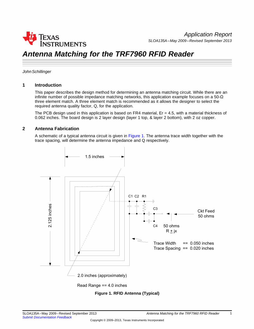
2 Antenna FabricationA schematic of a typical antenna circuit is given in Figure 1. The antenna trace width together with thetrace spacing, will determine the antenna impedance and Q respectively.
Figure 1. RFID Antenna (Typical)
1SLOA135A–May 2009–Revised September 2013 Antenna Matching for the TRF7960 RFID ReaderSubmit Documentation Feedback
Copyright © 2009–2013, Texas Instruments Incorporated

Antenna Fabrication www.ti.com
In this application, the antenna is fabricated on the top side of PCB. Some antenna designs will haveantenna traces on both top and bottom layers. In either case, it is important to keep ground planes awayfrom antenna traces or elements.
Notice that the antenna drawing (Figure 1) shows a diagonal measurement of approximately 2.0 inches. Arule of thumb is that the expected read range is twice the antenna diagonal measurement.
Figure 2. Antenna Bottom Layer Figure 3. Antenna Top Layer
2 Antenna Matching for the TRF7960 RFID Reader SLOA135A–May 2009–Revised September 2013Submit Documentation Feedback
Copyright © 2009–2013, Texas Instruments Incorporated

www.ti.com Antenna Impedance Matching
3 Antenna Impedance MatchingA three element match is used as it has the added advantage of allowing the circuit Q to be a chosenvalue.
Q = FO/BW = 13.56 MHz/2 MHz = 6.78 (1)
Where the required operating bandwidth is chosen at 2 MHz.
The first step in impedance matching is calibrating the network analyzer. This is done by connecting a RFtest connector on three blank circuit boards, one with a 50 load, second with a short (0-Ω resistor), andthird with an open. By using the application board in the calibration, PCB parasitic effects are accountedfor.
Following the calibration step, the antenna trace is connected to the test connector as required by 0-Ωresistors. The antenna trace is measured as shown in Figure 4; the resulting measurement is the startingimpedance which will be matched to 50 Ω.
Figure 4. Antenna Impedance = = (0.4648 Ω + j107.42) = = 1.2608 μH
The measured antenna impedance (0.4648 + j107.42) at 13.56 MHz is shown in Figure 4. Note that in thisapplication the antenna impedance is at the Smith Chart’s outer limit; or other wise stated the startingimpedance is up against the rail. This makes the impedance matching a little more difficult.
A minimum bandwidth (BW) of 2 MHz is chosen in order to accommodate the upper and lower RFIDsidebands for various data rates given in ISO15693 & ISO14443 A/B. Hence the approximate resistorvalue needed is determined as follows:
Q = FO/BW = 13.56 MHz/2 MHz = 6.78 (2)
Q = RP/XL = R/2 x π x 13.56 MHz x 1.2608 μH = R/107.42 (3)
Note that the XL value is the same as the measured Smith Chart value (107.42) from Figure 4.RP = Q x XL = 6.78 x 107.42 = 728 Ω (4)
Figure 5 is a Smith Chart impedance matching simulation.
3SLOA135A–May 2009–Revised September 2013 Antenna Matching for the TRF7960 RFID ReaderSubmit Documentation Feedback
Copyright © 2009–2013, Texas Instruments Incorporated

Imp 256 pF Shunt
10 25 50
Antenna Performace www.ti.com
Figure 5. Smith Chart Impedance Match Simulation
The measured impedance from Figure 4 is shown in Figure 5 as Imp 1. A shunt 56-pF capacitor rotatesthe impedance to Imp 2. Next a shut resistor (which sets the antenna Q or BW), rotates the impedancefrom Imp 2 to Imp 3; where the impedance is now on the 50-Ω circle. The final matching element is a 56-pF capacitor, which rotates the impedance from Imp 3 to Imp 4 (46.6 + j0.3). This capacitor is split into twoparallel caps (47 pF + 10 pF) to allow fine tuning of the antenna frequency while also reducing componentparasites.
Note earlier the shut resistor was calculated to be 728 Ω whereby it is now rounded to up to 1.0 KΩ inorder to yield a match with standard capacitor values.
Final circuit values for the antenna circuit given in Figure 1 are as follows:
C1 = = 56 pF
C2 = = DNP (Do Not Place)
R1 = = 1 .0 KΩ
C3 = = 47 pF
C4 = = 10 pF
4 Antenna Performace
4 Antenna Matching for the TRF7960 RFID Reader SLOA135A–May 2009–Revised September 2013Submit Documentation Feedback
Copyright © 2009–2013, Texas Instruments Incorporated

www.ti.com Antenna Performace
Figure 6. Smith Chart Figure 7. Return Loss(50.635 - j804.67) = = 14.586 nF (RL = 40 dB at 13.56 MHz)
Note that Figure 7 shows a 10 dB return loss over a 1.0124-MHz BW (Mkr 3-2). A rule of thumb is that theantenna 3-dB BW is twice the 10-dB return loss bandwidth. Applying the rule to this application wouldyield an antenna bandwidth of 2.248 MHz.
Figure 8. Polar Plot Figure 9. VSWR Plot
5SLOA135A–May 2009–Revised September 2013 Antenna Matching for the TRF7960 RFID ReaderSubmit Documentation Feedback
Copyright © 2009–2013, Texas Instruments Incorporated

Antenna Performace www.ti.com
Figure 10. Linear Plot Figure 11. Phase Plot
Figure 12. Real Part Figure 13. Imaginary Part
6 Antenna Matching for the TRF7960 RFID Reader SLOA135A–May 2009–Revised September 2013Submit Documentation Feedback
Copyright © 2009–2013, Texas Instruments Incorporated
www.ti.com Antenna Performace
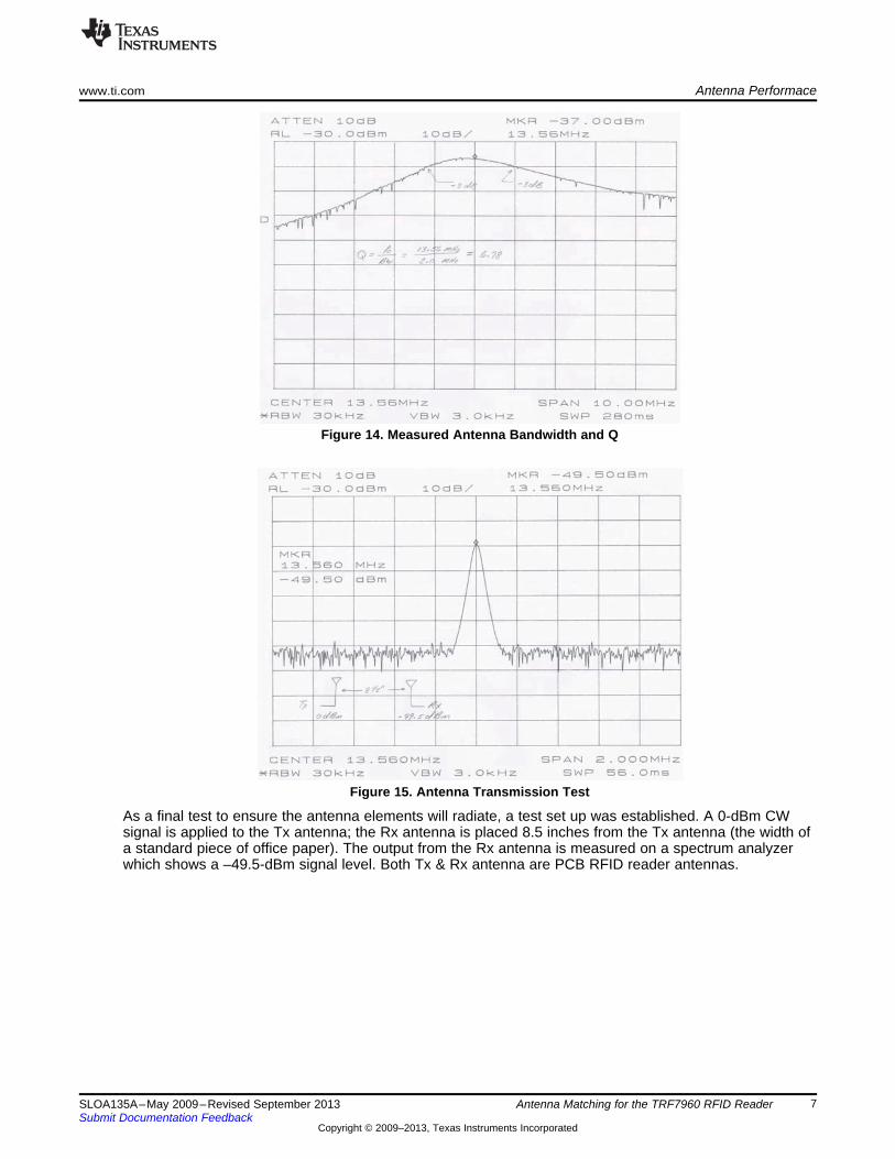
Figure 14. Measured Antenna Bandwidth and Q
Figure 15. Antenna Transmission Test
As a final test to ensure the antenna elements will radiate, a test set up was established. A 0-dBm CWsignal is applied to the Tx antenna; the Rx antenna is placed 8.5 inches from the Tx antenna (the width ofa standard piece of office paper). The output from the Rx antenna is measured on a spectrum analyzerwhich shows a –49.5-dBm signal level. Both Tx & Rx antenna are PCB RFID reader antennas.
7SLOA135A–May 2009–Revised September 2013 Antenna Matching for the TRF7960 RFID ReaderSubmit Documentation Feedback
Copyright © 2009–2013, Texas Instruments Incorporated

IMPORTANT NOTICE
Texas Instruments Incorporated and its subsidiaries (TI) reserve the right to make corrections, enhancements, improvements and otherchanges to its semiconductor products and services per JESD46, latest issue, and to discontinue any product or service per JESD48, latestissue. Buyers should obtain the latest relevant information before placing orders and should verify that such information is current andcomplete. All semiconductor products (also referred to herein as “components”) are sold subject to TI’s terms and conditions of salesupplied at the time of order acknowledgment.
TI warrants performance of its components to the specifications applicable at the time of sale, in accordance with the warranty in TI’s termsand conditions of sale of semiconductor products. Testing and other quality control techniques are used to the extent TI deems necessaryto support this warranty. Except where mandated by applicable law, testing of all parameters of each component is not necessarilyperformed.
TI assumes no liability for applications assistance or the design of Buyers’ products. Buyers are responsible for their products andapplications using TI components. To minimize the risks associated with Buyers’ products and applications, Buyers should provideadequate design and operating safeguards.
TI does not warrant or represent that any license, either express or implied, is granted under any patent right, copyright, mask work right, orother intellectual property right relating to any combination, machine, or process in which TI components or services are used. Informationpublished by TI regarding third-party products or services does not constitute a license to use such products or services or a warranty orendorsement thereof. Use of such information may require a license from a third party under the patents or other intellectual property of thethird party, or a license from TI under the patents or other intellectual property of TI.
Reproduction of significant portions of TI information in TI data books or data sheets is permissible only if reproduction is without alterationand is accompanied by all associated warranties, conditions, limitations, and notices. TI is not responsible or liable for such altereddocumentation. Information of third parties may be subject to additional restrictions.
Resale of TI components or services with statements different from or beyond the parameters stated by TI for that component or servicevoids all express and any implied warranties for the associated TI component or service and is an unfair and deceptive business practice.TI is not responsible or liable for any such statements.
Buyer acknowledges and agrees that it is solely responsible for compliance with all legal, regulatory and safety-related requirementsconcerning its products, and any use of TI components in its applications, notwithstanding any applications-related information or supportthat may be provided by TI. Buyer represents and agrees that it has all the necessary expertise to create and implement safeguards whichanticipate dangerous consequences of failures, monitor failures and their consequences, lessen the likelihood of failures that might causeharm and take appropriate remedial actions. Buyer will fully indemnify TI and its representatives against any damages arising out of the useof any TI components in safety-critical applications.
In some cases, TI components may be promoted specifically to facilitate safety-related applications. With such components, TI’s goal is tohelp enable customers to design and create their own end-product solutions that meet applicable functional safety standards andrequirements. Nonetheless, such components are subject to these terms.
No TI components are authorized for use in FDA Class III (or similar life-critical medical equipment) unless authorized officers of the partieshave executed a special agreement specifically governing such use.
Only those TI components which TI has specifically designated as military grade or “enhanced plastic” are designed and intended for use inmilitary/aerospace applications or environments. Buyer acknowledges and agrees that any military or aerospace use of TI componentswhich have not been so designated is solely at the Buyer's risk, and that Buyer is solely responsible for compliance with all legal andregulatory requirements in connection with such use.
TI has specifically designated certain components as meeting ISO/TS16949 requirements, mainly for automotive use. In any case of use ofnon-designated products, TI will not be responsible for any failure to meet ISO/TS16949.
Products Applications
Audio www.ti.com/audio Automotive and Transportation www.ti.com/automotive
Amplifiers amplifier.ti.com Communications and Telecom www.ti.com/communications
Data Converters dataconverter.ti.com Computers and Peripherals www.ti.com/computers
DLP® Products www.dlp.com Consumer Electronics www.ti.com/consumer-apps
DSP dsp.ti.com Energy and Lighting www.ti.com/energy
Clocks and Timers www.ti.com/clocks Industrial www.ti.com/industrial
Interface interface.ti.com Medical www.ti.com/medical
Logic logic.ti.com Security www.ti.com/security
Power Mgmt power.ti.com Space, Avionics and Defense www.ti.com/space-avionics-defense
Microcontrollers microcontroller.ti.com Video and Imaging www.ti.com/video
RFID www.ti-rfid.com
OMAP Applications Processors www.ti.com/omap TI E2E Community e2e.ti.com
Wireless Connectivity www.ti.com/wirelessconnectivity
Mailing Address: Texas Instruments, Post Office Box 655303, Dallas, Texas 75265Copyright © 2013, Texas Instruments Incorporated