annual report 2004 solid-state electronics department · annual report 2004 - solid-state...
TRANSCRIPT

Annual Report 2004
Solid-State Electronics Department Prof.Dr.rer.nat. F.J.Tegude
Universität Duisburg-Essen Fakultät für Ingenieurwissenschaften
Institut für Technologien der Informationstechnik
Halbleitertechnik/Halbleitertechnologie
Lotharstrasse 55 / ZHO D-47057 Duisburg
Germany
Tel.: ++49 (0)203 379 3392 (Secr.) Fax: ++49 (0)203 379 3400 email: [email protected] www: http://www.zho.uni-duisburg.de
Editors: Dr.-Ing. Werner Prost Dr.-Ing. Wolfgang Brockerhoff
Halbleitertechnik/Halbleitertechnologie


Annual Report 2004 - Solid-State Electronics Department
Table of Contents 1 Preface ........................................................................................................................................ 1
2 Members of the Department ...................................................................................................... 3
3 Teaching Activities..................................................................................................................... 5
3.1 Lectures and Laboratory Exercises ............................................................................................ 5
3.2 Student Reports and Diploma Thesis ......................................................................................... 8
3.3 Doctor Thesis.............................................................................................................................. 9
3.4 Seminar on Semiconductor Electronics.................................................................................... 10
4 Research Activities .................................................................................................................. 13
4.1 Epitaxial Growth and Materials ........................................................................................... 13
4.1.1 MOVPE Growth and HRXRD Characterisation of GaAsSb/InP Superlattice S. Neumann ................................................................................................................ 14
4.1.2 Influence of Nitrogen Carrier Gas on the Growth of GaAsSb:C S. Neumann ................................................................................................................ 17
4.1.3 InAlAs/InGaAs Resonant Tunneling Diodes on Si Substrate V. Khorenko, R.Geitmann ......................................................................................... 20
4.1.4 Growth of Nano-Whiskers on Different Substrates by MOVPE I. Regolin, S. Neumann .............................................................................................. 23
4.1.5 Development of Automation Software for Photoluminescence Set-Up L. Kumfa, V. Khorenko.............................................................................................. 26
4.2 Device and Circuit Processing................................................................................ 29
4.2.1 Fabrication and Charactarization of In-P-based Enhancement-type Heterostructure Field Effect Transistors (E-HFET) R. Schlangen, Q.T. Do ............................................................................................... 30
4.2.2 Optimisation of the Oxygen Plasma Cleaning Process Used for Sub Micrometer Gate Length on Heterojunction Field Effect Transistors J. Henze, J. Degenhardt .............................................................................................. 33
4.2.3 Influence of Layout Considerations on the HBT RF Device Performance J. Driesen, S. Topaloglu ............................................................................................. 36
4.2.4 Optimisation of Process To Reduce Parasitic Components of Heterojunction Bipolar Transistors (HBT) A. Poloczek, S. Topaloglu.......................................................................................... 39
4.2.5 Investigation of Wet Etching Parameters to Optimise The HBT Process S. Topaloglu ............................................................................................................... 42
4.2.6 Installation and First InP/InGaAs Dry Experiments with ICP-RIE S. Topaloglu ............................................................................................................... 46

Annual Report 2004 - Solid-State Electronics Department
4.2.7 Manufacturability and Electrical Characteristics of Si/SiGe Interband Tunnelling Diodes E. Khorenko, M. Stoffel, O.G. Schmidt, G. Klimeck, H.Barbknecht ........................ 49
4.2.8 Design and Realization of Characterization- and Burn-In-Setup for the Evaluation of GaN-High-Power-Fieldeffect Transistors for Satellite Communications in the X-Band M. Rostewitz, W. Brockerhoff. .................................................................................. 52
4.3 Device and Circuit Simulation, Measurement and Modelling ........................... 55
4.3.1 Bias Dependent Noise Model for HBT S. Ehrich ..................................................................................................................... 56
4.3.2 Design, Layout and Charaterization of an Automatic Gain Amplifier M. Brysch. J.Driesen ................................................................................................. 59
4.3.3 Creation and Adaption of a Model for RTBT for Circuit Simulation A. Viessmann, S. Ehrich ............................................................................................ 62
4.3.4 Digital Logic Circuits Based on Resonant-Tunneling Bipolar-Junction-Transistors Ch. Prusinski, A.Matiss ............................................................................................. 65
4.3.5 Boolean Logic Application of Resonant-Tunneling Bipolar Junction Transistors A. Matiss, J.Driesen, S.Ehrich ................................................................................... 68
4.3.6 Investigation of Self-Oscillation of Resonant Tunneling Devices T. Geistert, A. Matiss ................................................................................................ 71
4.3.7 Optical Measurements of MOBILE with CW-Laser A. Matiss, E.Khorenko............................................................................................... 74
4.4 Nanoelectronics......................................................................................................... 77
4.4.1 Photoluminescence Characterisation of GaAs Nano-Whiskers on Si Substrate V. Khorenko, I.Regolin .............................................................................................. 78
4.4.2 Integration of an Aerosol Generator in the MBE V. Khorenko, R. Geitmann, C. Klein ......................................................................... 81
4.4.3 Selfgating Effect in a Novel Nanometer Scale Semiconductor Device Utilizing an Asymmetric 2-DEG Channel T. Do........................................................................................................................... 84
4.4.4 Enhancement of an Scanning Force Microscope for I/V-Measurement on Nanoelectronic Components H.G. Kreusch Q.T.Do................................................................................................. 87
4.4.5 Probing Carriers in Low-Dimensional Systems with High Spatial Resolution by Novel Scanning Probe Techniques S. Bonsels, S. Anand1, O. Douheret1, 1KTH Stockholm........................................... 90

Annual Report 2004 - Solid-State Electronics Department
4.5 Conference Contributions......................................................................................................... 93
4.6 Publications ............................................................................................................................. 95
4.7 Research Projects ..................................................................................................................... 98
4.8 Other Activities ........................................................................................................................ 99
5 Guide to the Solid-State Electronics Department .................................................................. 101


Annual Report 2004 - Solid-State Electronics Department 1
1 Preface
This report presents the teaching and research activities of the Solid State Electronics Department (Fachgebiet Halbleitertechnik/Halbleitertechnolgie) during the year 2004. This year again was characterized by evaluation and reorganization, on the one hand to establish the merger between the formerly seperated universities of Duisburg and Essen into one on faculty level, and on the other hand to prepare and start new curricula and related teaching activities, especially aiming at an international profile. Foreign students in our Electrical and Information/Communication Engineering Department nowadays make up about 60%.
Research activities with respect to established devices, like Heterostructure-Fieldeffect-Transistors (HFETs) and Single-Heterostructure-Bipolar-Transistors (SHBTs), are more and more concen-trating on circuit applications for high speed digital and analog circuits. To this end our facilities have been improved by establishing a new ICP-Reactive Ion Etching system, also in order to achieve higher yield and reproducibility, especially for downscaled devices. For HBTs with submicron emitter width, the reduction of parasitics is increasingly important, and this has been successfully addressed in design and layout as well as in process optimization. Nevertheless, growth and process developments of GaAsSb based Double-Heterostructure-BTs (DHBTs), still are challenging tasks.
On the other hand increasing effort has been put on nanomaterials and –structures. Among other activities we have started to grow III-V-nanowires (“nano-whiskers”) on III-V as well as on silicon substrates, and achieved excellent material quality. We also developed a method to contact single whiskers allowing to study transport mechanisms through 1-dimensional structures. This is an additional approach to combine silicon and III-V based technologies besides III-V-growth on silicon substrates and Si/SiGe-RTDs. These activities can open up new application oriented research areas and cost efficient processing opportunities.
Finally, I want to thank friends and partners everywhere for their support and cooperation, and last, but not least, all students and members of the Solid State Electronics Department for their efforts and contributions.
Duisburg, April 2005
Prof. Dr. rer. nat. F.-J. Tegude

2 Annual Report 2004 - Solid-State Electronics Department

Annual Report 2004 - Solid-State Electronics Department 3
2 Members of the Department
379- office email
head of the department
Prof. Dr.rer.nat. Franz-Josef Tegude - 3391 LT 207 [email protected]
secretary
Dagmar Birke - 3392 LT 206 [email protected]
scientific staff
Dr.-Ing. Wolfgang Brockerhoff (AOR) - 2989 LT 205 [email protected]
Dipl.-Phys. Jan Degenhardt until 06/04
Dipl.-Phys. Quoc Thai Do - 3393 LT 106 [email protected]
Dipl.-Ing. Jörn Driesen - 2491 LT 218 [email protected]
Dipl.-Ing. Silja Ehrich - 3881 LT 204 [email protected]
Dipl.-Ing. Georg Grah until 12/04
Dr. Zhi Jin until 02/04
Dr.-rer.nat. Victor Khorenko - 3877 LT 104 [email protected]
M.Sc. Evgenia Khorenko until 12/04
Dipl.-Ing. Andreas Matiss - 4605 LT 203 [email protected]
Dipl.-Phys. Stefan Neumann until 12/04
Dr.-Ing. Werner Prost - 4607 LT 205 [email protected]
Dipl.-Ing. Ingi Regolin - 3877 LT 104 [email protected]
Dipl.-Ing. Björn Schlothmann
M.Sc. Serkan Topaloglu - 2492 LT 218 [email protected]
technical staff
Udo Doerk - 3395 LT 202 [email protected]
Dipl.-Ing. Ralf Geitmann - 4604 LT 202 [email protected]
Dipl.-Ing. Wolfgang Molls - 4603 LT 201 [email protected]
Andrea Osinski - 4600 LT 104 [email protected]
Ing. (grad.) Reimund Tilders - 3396 LT 201 [email protected]

4 Annual Report 2004 - Solid-State Electronics Department
apprentices
Claudia Schmidt until 07/04 - 4095 LT 106 [email protected]
Jana Bödige until 07/04 - 4618 LT 106 bö[email protected]
Sarah Dohle since 09/04 - 4095 LT 106 [email protected]
Florian Dippe since 09/04 - 4618 LT 106 [email protected]
students
Augustine Che Mofor until 02/04
Michael Tekloth until 10/04
Thorsten Scholz until 06/04
Lars Schneider until 03/04
Thomas Fischle until 04/04
Christoph Prusinski until 09/04
Johannes Henze until 10/04
Ingo Nannen
Christoph Kandler since 10/04
Abu Shariha Luay since 10/04
Thomas Geistert
André Krowas
Björn Rasmussen
Matthias Meier
Benjamin Hoffmann

Annual Report 2004 - Solid-State Electronics Department 5
3 Teaching Activities 3.1 Lectures and Laboratory Exercises
Schedule International Studies in
Engineering (ISE) Lectures and exercises diploma course
B.Sc. M.Sc
Solid-State Electronics 1 Festkörperelektronik 1 3rd sem.
Solid-State Electronics 2 Festkörperelektronik 2 4th sem.
Introduction to Solid-State Electronics Einführung in die Festkörperelektronik 4th sem.
Technical Electronics 1 Technische Elektronik 1 5th sem.
Basic Electronic Devices Grundlagen Elektronischer Bauelemente 3rd / 5th
sem.
Technical Electronics 2 Technische Elektronik 2 6th sem.
Basic Electronic Circuits Grundlagen Elektronischer Schaltungen 2nd sem.
Semiconductor Microelectronics Technology 1/ III-V Technologies and Components 1/ Halbleitertechnologie 1
optional
Laboratory exercises
Communication Electronics Praktikum Technische Elektronik 7th sem.
Introduction to Operational Amplifiers Praktikum Operationsverstärker
6th/8th sem.
(optional)optional
Semiconductor Technology Praktikum Halbleitertechnologie/ Halbleitertechnologie 2
8th sem. (optional) optional
Basic Electronic Devices Praktikum Grundlagen Elektronischer Bauelemente 3rd / 5th
sem.
Basic Electronic Circuits Praktikum Grundlagen Elektronischer Schaltungen 2nd sem.
Seminars and Colloquia
Seminar on Semiconductor Electronics Probleme der modernen Halbleiterphysik
Seminar on Epitaxial Problems

6 Annual Report 2004 - Solid-State Electronics Department
Lectures and Exercises:
Introduction to Solid-State Electronics / Solid-State Electronics 1,2 (Einführung in die Festkörperelektronik) / (Festkörperelektronik 1,2)
These courses start with an introduction to the basics of Quantum physics. Based on Schroedinger's equation and Heisenberg's uncertainty relations a comprehensive understanding of semiconductor band structure is achieved. The first part (Introduction to Solid-State Electronics) also includes carrier statistics and ends up with a discussion of current continuity and Poisson's equation. In the second part of this lecture the basic building blocks of electronic devices, i.e. semiconductor-metal contact, MIS system, pn junction and heterostructures, are treated for subsequent courses on field effect and bipolar electronics.
Basic Electronic Devices (Technische Elektronik 1)
MOS-Capacitors, charge coupled devices and Field-Effect Transistors both, on Silicon and III/V material, are treated during the first part of the course. The fundamentals as well as the DC characteristics of MOSFET, MESFET, JFET, and Heterostructure FET (HFET) are derived and analysed in detail.
Additionally, bipolar devices - pn-diodes, npn- and pnp-transistors as well as tunnel- and zener-diodes - are considered. Based on the dc characterisitics simple small-signal equivalent circuits are derived.
Basic Electronic Circuits (Technische Elektronik 2)
This course covers the basic methods to calculate complex electronic circuits using the devices treated within the "Basic Electronic Devices". Various device models with respect to circuit design and circuit simulation using commercial circuit simulation tools are discussed. Numerous analog (e.g. operational amplifiers) and digital applications are included.
Semiconductor Microelectronics Technology 1,2 (Halbleitertechnologie 1,2)
The semiconductor microelectronics technology lectures are devoted to III/V-semiconductor heterostructures for high speed electronic devices. The process steps from crystal growth to circuit fabrication are discussed. The first semester is focused on heterostructure material issues. Modern growth techniques like molecular beam epitaxy (MBE) and metal-organic vapour-phase epitaxy (MOVPE) are discussed in terms atomic layer control of thickness, composition, and doping. High Resolution X-ray diffraction, photoluminescence, and ellipsometry are explained for non-destructive material assessment in the mono-layer scale. The second semester is devoted to microelectronic fabrication techniques for high speed (f ≥100 GHz) devices and circuits. The lateral and vertical processing of epitaxial films, insulating layers, and metallizations are presented for high performance monolithic high speed analog and digital integrated circuits.

Annual Report 2004 - Solid-State Electronics Department 7
Laboratory exercises
Communication Electronics, Basic Electronic Devices, Basic Electronic Circuits (Praktikum Technische Elektronik)
Within the laboratory exercises students apply their theoretical knowledge based on the lectures "Basic Electronic Devices" and "Basic Electronic Circuits". The capacitance-voltage characteristics of schottky diodes are measured and evaluated. The dc and small signal parameters of bipolar transistors as well as the switching behaviour is experimentally investigated. The course also covers the analysis of the dynamical performance of digital circuits. Additionally, numerical simulations and synthesis of basic electronic circuits are carried out on a UNIX system.
Introduction to Operational Amplifiers (Praktikum Operationsverstärker)
The aim of this course is the understanding of the basic principles and the characteristics of operational amplifiers (OpAmps). The laboratory exercises demonstrate their applicability in electronic circuits enabling the students to an independent design and understanding of complex circuits. Starting with the measurement and interpretation of the most important characteristic parameters of OpAmps, circuits like adders and multipliers, amplifiers and active filters are intensively calculated and investigated. Oscillators and generators are designed and measured.
Seminars and Colloquia
Seminar on Semiconductor Electronics (Probleme der modernen Halbleiterphysik)
Within this seminar actual topics of the semiconductor electronics are discussed. Students, but also members of the department, report about their own work.
Seminar on Epitaxial Problems
Problems of the epitaxial growth of semiconductor structures are analysed, results are interpreted and future trends are discussed.
Colloquium on Optoelectronics Recent developments and problems in the Optoelectronics/Photonics field and neighboured topics are presented by invited experts from all over the world.

8 Annual Report 2004 - Solid-State Electronics Department
3.2 Student Reports and Diploma Thesis (Studien-/Diplomarbeiten)
Student reports
TEKLOTH, MICHAEL
Evaluierung eines Kleinsignal-Modells für ITD January 2004
PRUSINSKI, CHRISTOPH
Optimierung und Erweiterung der Schaltung für einen spannungsgesteuerten Oszillator February 2004
HENZE, JOHANNES
Optimierung des Sauerstoff-Plasma Reinigungsprozesses für den Einsatz beim submikrometer Gate-Recess an Heterostruktur-FET March 2004
VIESSMANN, ALEXANDER
Erstellung und Anpassung eines Modells für RTBT March 2004
KUMFA, LAWRENCE
Entwicklung eines automatisierten Photolumineszenzmessplatzes für die Charakterisierung von III-V Halbleiterschichten May 2004 Diploma thesis
MOFOR, AUGUSTINE
Wachstum und Charakterisierung von III/V-Bauelementschichten auf Si Substraten January 2004
SCHLANGEN, RUDOLF
Herstellung und Charakterisierung von Anreicherungstyp Heterostruktur-FET auf InP-Substrat April .2004
KREUSCH, HANS-GERD
Erweiterung eines Rasterkraftmikroskops zur Aufnahme von IU-Messungen an nanoelektro-nischen Bauelementen August 2004
BRYSCH, MICHAEL
Design, Layout und Charakterisierung eines Verstärkers mit automatischer Nachführung des Ausgangspegels July 2004

Annual Report 2004 - Solid-State Electronics Department 9
BONSELS, STEFAN
Lateral hochauflösende elektrische Charakterisierung von III-V Halbleiter Quantenstrukturen August 2004
REGOLIN, INGO
Epitaktisches Wachstum von Nanowhiskern mit der MOVPE August 2004
POLOCZEK, ARTUR
Entwicklung von Prozessen zur Reduzierung der parasitären Komponenten von Heterostruktur-Bipolartransistoren# November 2004
ROSTEWITZ, MIRKO
Konzeption und Aufbau von Mess- und Burn-In-Einrichtungen zur Evaluation von GaN-High Power Feldeffekttransistoren für die Satellitenkommunikation im X-Band December 2004
PRUSINSKI, CHRISTOPH
Digitale logische Schaltungen auf Basis von Resonanztunnel-Bipolartransistoren December 2004
3.3 Doctor Thesis
REIMANN, THORSTEN Monolithische Integration von Heterostruktur-Bipolartransistoren und Elektroabsorptions-modulatoren auf InP February 2004

10 Annual Report 2004 - Solid-State Electronics Department
3.4 Seminar on Semiconductor Electronics
08.01.2004 J.DEGENHARDT, G.GRAH, REPORT ON THE PROJECT 'A/D converter in superconductor-semiconductor hybrid technology (SUPER-ADC)'
15.01.2004 A.M.MOFOR, REPORT ON THE DIPLOMA THESIS: 'Wachstum und Charakterisierung von III/V-Bauelementschichten auf Si Substraten'
S. EHRICH, REPORT ON THE PROJECT 'DC- und AC-Modellierung von InP basierenden Heterostruktur-Bipolar-transistoren'
22.01.2004 M. TEKLOTH, REPORT ON THE STUDENT THESIS: Evaluierung eines Kleinsignal-Modells für Interband Tunneling Diodes
22.04.2004 ALEXANDER VIESSMANN, REPORT ON THE STUDENT THESIS: 'Klein-/Großsignalmodellierung von RTBT, Nachsimulation von Schaltungen mittels ADS'
JOHANNES HENZE, REPORT ON THE STUDENT THESIS: 'Optimierung des Sauerstoff-Plasma Reinigungsprozesses für den Einsatz beim submikrometer
Gate-Recess an Heterostruktur-FET'
CHRISTOPH PRUSINSKI, REPORT ON THE STUDENT THESIS: 'Optimierungund Erweiterung der Schaltung für einen spannungsgesteuerten Oszillator'
04.05.2004, RUDOLF SCHLANGEN, REPORT ON THE DIPLOMA THESIS: 'Herstellung und Charakterisierung von Anreicherungstyp Heterostruktur-FET auf InP-Substrat'
17.06.2004 LAWRENCE KUMFA, REPORT ON THE STUDENT THESIS: 'Entwicklung eines automatisierten Photolumineszenzmessplatzes für die Charakterisierung von III-V Halbleiterschichten'
15.07.2004 MICHAEL BRYSCH, REPORT ON THE DIPLOMA THESIS: 'Design, Layout und Charakterisierung eines Verstärkers mit automatischer Nachführung des Ausgangspegels'

Annual Report 2004 - Solid-State Electronics Department 11
27.07.2004 STEFAN NEUMANN, REPORT ON THE CONFERENCE: '12th Int. Conf on Metalorganic Vapour Phase Epitaxy ( ICMOVPE)', Lahaina, Hawaii, USA, 30.05.2004-04.06.2004
VICTOR KHORENKO, REPORT ON THE CONFERENCE: '16th Int. Conf. on InP and Related Materials ( IPRM), Kagoshima, Japan, 31.05.2004-04.06.2004, Kagoshima, Japan, 31.05.2004- 04.06.2004'
29.07.2004 STEFAN BONSELS, REPORT ON THE DIPLOMA THESIS: 'Lateral hochauflösende elektrische Charakterisierung von III-V Halbleiter Quantenstrukturen'
SILJA EHRICH, REPORT ON THE CONFERENCE: 'Fluctuations and Noise', Gran Canaria, 25.05.04-28.05.04
14.10.2004 INGO REGOLIN, REPORT ON THE DIPLOMA THESIS: 'Epitaktisches Wachstum von Nanowhiskern mit der MOVPE'
SERKAN TOPALOGLU, JÖRN DRIESEN, REPORT ON THE PROJECT "InP basierende Heterostruktur Biolartransistoren (HBT)"
21.10.2004 HANS-GERD KREUSCH, REPORT ON THE DIPLOMA THESIS: 'Erweiterung eines Rasterkraftmikroskops zur Aufnahme von IU-Messungen an nanoelektronischen Bauelementen'
02.11.2004 STEFAN KRÄMER (UNIVERSITÄT ERLANGEN, TECHNISCHE PHYSIK), REPORT ON Polarisationsschalter hoher Empfindlichkeit im Wellenlängenbereich von 1,3µm
04.11.2004 ANDREAS MATISS, REPORT ON THE CONFERENCE: 'European Microwave Week ( EuMW), Amsterdam, NL, 11.10.2004-15.10.2004
EVGENIA KHORENKO, VICTOR KHORENKO, REPORT ON THE CONFERENCE: 'The Fifth International Conference
on Advanced Semiconductor Devices and Microsystems ( ASDAM '04), Smolenice, Slovakia, 17.10.2004-21.10.2004
16.11.2004 T.MÜLLER, Q.T.DO, REPORT ON Selfgating: a step towards ultra-fast switching nano semiconductor devices
16.12.2004 VICTOR KHORENKO, REPORT ON THE CONFERENCE: 'Deutscher MBE Workshop 2004 ( 2004), Braunschweig, Germany, 11.10.2004-12.10.2004
INGO REGOLIN, REPORT ON THE CONFERENCE: 'DGKK Workshop ( 2004), Freiburg, Germany, 09.12.2004-10.12.2004

12 Annual Report 2004 - Solid-State Electronics Department

Annual Report 2004 - Solid-State Electronics Department 13
4 Research Activities
4.1 Materials, Growth and Characterization

14 Annual Report 2004 - Solid-State Electronics Department
4.1.1 MOVPE growth and HRXRD characterisation of GaAsSb/InP superlattice
Scientist: S. Neumann
Backround The low bandgap material GaAsxSb1-x (x < 0.73) forms a type-II staggered heterojunction with InP [1]. This characteristic and its ultra-high p-type doping capability make this material ideal as the base layer in InP-based heterostructure bipolar transistor (HBT) structures. The ternary III/V semiconductor GaAsxSb1-x has a solid phase miscibility gap ranging from x = 0.2 to 0.8 [2]. Using MBE and MOVPE the metastable growth of GaAsSb lattice matched on InP has been demonstrated [2]. The use as base material in InP based HBT was first demonstrated in 1996 [3]. A staggered heterojunction line up enables the use of InP as emitter and collector. Basic double heterostructure bipolar transistor (DHBT) structures can be realized with the advantages of low turn-on and high break down voltages [4]
The most challenging step in the MOVPE growth of InP/GaAsSb/InP heterostructures for DHBT application is the optimisation of the most critical GaAsxSb1-x/InP heterojunction forming the base and emitter layer in a HBT structure. Posibel Sb and As segregation and desorption results in formation of interlayers which may degrade the performance of devices. A growth interruption between the GaAsxSb1-x base layer and the following InP emitter layer with group V stabilization of the surface leads to Sb contamination of the surface and to strong segregation of the Sb into the InP emitter layer [5]. To prevent this effect, a surface stabilization with Sb is impossible. The stabilization with As as group V element, only, leads also to a possible GaAs interlayer with the out diffusion of Sb at the surface region. Results from molecular beam epitaxie (MBE) indicate the As to Sb exchange resulting in highly strained and degraded interfacial layers [6]. In this work we investigated the formation of the GaAsSb/InP interface grown by MOVPE using nitrogen as carrier gas. Superlattice structures with different growth interruptions were realized and characterized with high resolution x-ray diffraction.
Experimental Setup The experiments were done on semi insulating, exactly oriented (001) InP substrate in a AIX 200 reactor with RF heating at a substrate temperature of Tg = 550 °C. Purified nitrogen (N2) as carrier gas was used to adjust the reactor pressure of ptot= 50 mbar at a total flow of Qtot= 3.4 slm. Hydrogen was connected to the source gas line, only. We used a complete non gaseous source configuration with tertiarybutylphosphine (TBP) / tertiarybutylarsine (TBAs) / trimethylantimony (TMSb) as group V sources, carbon tetrabromide (CBr4) as group IV doping sources and the metal-organic sources trimethylindium (TMIn) / triethylgallium (TEGa). The group V to group III ratios (V/III) and also the group IV to group III ratios (IV/III) were calculated from the ratio of the partial pressures of the precursors involved. For the determination of the antimony (Sb) concentration in the partial highly strained GaAsSb interlayers high resolution x-ray diffractometry (HRXRD) was used. The integrity of the layer structures is proven by HRXRD measurements in the vicinity of the

Annual Report 2004 - Solid-State Electronics Department 15
004 and 002-reflection in a coupled Θ-2Θ-mode using a double monochromator set-up. The recorded reflection curves were compared to simulations using commercial software.
Results and Discussion The growth of GaAsxSb1-x/InP superlattice with nitrogen as carrier gas at a growth temperature of Tg= 550°C was investigated. At this growth temperature the cracking of TBP is incomplete. We used a V/III ratio of V/III=80 and a growth rate of r=5 nm/min to obtain InP layers with a mirror like surface. The GaAsSb layers were grown with a V/III ratio of V/III=0.8. A IV/V ratio of IV/V=8.4% resulted in a doping level of p=4x1019 cm –3. Figure 1 shows the high resolution x-ray
diffraction curves in the vicinity of the (004) - and the (002) - reflection of a selected GaAsSb/InP superlattice. We simulate both reflections with one set of parameters. Equal layers, which were grown under the same growth conditions, are coupled to minimize the number of free parameters. This enables us to determine the composition and the layer thickness of each layer. The period of the fringes can be associated to single layers of the superlattice structure. The determined values of composition and thickness (layer parameter) are in good agreement with the intended data. The simulation of the x-ray data of this layer stack shows an excellent agreement to the measured curves. To optimize the emitter base junction, a TBAs purge between the GaAsSb:C base layer and the following InP layer was included. To force a change of the possible interlayer we varied the purge time from tp = 1 s to tp = 60 s. We observed, that after a short purge a stable As rich GaAsxSb1-x interlayer with a average composition of x ≈ 90 occurs. A summary of the experimental results is given in Table 1. The composition is outside the solid phase miscibility gap for the used growth temperature of Tg=550°C. Independent of the purge time, we can not observe a trend of the composition or thickness of this interlayer which has an average thickness of tinterlayer= 7 Å.
Fig. 6 X-ray recorded and simulated reflectedintensity in the vicinity of InP (004) and (002)reflextion of a superlattice structure (10 x 6 nm InP / 31 nm GaAs0.46Sb0.54 grown with 1 s As purge at thegrowth interruption. An optimum agreement isobtained for a 0.9 nm thick GaAs interlayer.

16 Annual Report 2004 - Solid-State Electronics Department
Probe Growth interruption Composition Interlayer thickness M3148 1s GaAs0.95Sb0.05 0.9 nm M2990 5 s GaAs1.0Sb0.0 0.3 nm M3076 10 s GaAs0.86Sb 0.14 0.4 nm M3077 30 s GaAs0.89Sb 0.11 0.8 nm M3078 60 s GaAs0.91Sb 0.09 0.6 nm
Table 1: Simulation results of the interface composition and thickness between GaAsSb and InP heterostructures
These results were confirmed independent by reflectance anisotropy (RA) spectroscopy and low-energy electron diffraction (LEED) [7]. The As terminated surface lead to a typical GaAs reconstructed surface. Growth of GaAsSb with a tp=10 s, TBAs stabilized growth interruption lead to similar results [8]. A fast change in the RA spectrum could be observed resulting in a 0.76 nm thick GaAs interlayer. All grown superlattic shown a mirror like surface and the HRXRD measurement prove the high crystal quality. To prevent the critical GaAsxSb1-x/InP heterojunction for possible contamination a short growth interruptions is preferable.
Conclusion A novel growth method for the fabrication of GaAsSb/InP heterostructures using nitrogen as carrier gas has been elaborated. It has been demonstrated that the segregations of Sb is controllable. To prevent a segration of Sb in following layers an As purge after the growth of GaAsxSb1-x is necessary. This forms a thin GaAs like interlayer between GaAsxSb1-x and the following layer.
References: [1] M. Peter, N. Herres, F. Fuchs, K. Winkler, K.-H. Bachem, J. Wagner;“ “ , Appl. Phys. Lett, Vol. 74
(3), 1999 [2] M. J. Cherng, R. M. Cohen, G. B. Stringfellow;” ”, J. of Electronic Materials, Vol. 13, No. 5, 1984 [3] R. Bhat, W-P. Hong, C. Caneau, M. A. Koza, C-K. Nguyen, S. Goswami;” “, Appl. Phys. Lett, Vol.
68 (7), 1996 [4] C. R. Bolognesi, N. Matine, X.G. Xu, G. Soerensen, S. Watkins;” “, Microelectronics Reliability, 39
(1999) 1833-1838 [5] C.X. Wang, O.J. Pitts, S.P. Watkins;” “, J. Crystal Growth,Vol. 248, 2003 [6] R. Kaspi;”Compositional abruptness at the InAs-GaSb interface: optimizing growth by using the Sb
desorbtion signatur“,J. Crystal Growth, Vol. 201/202, 1999 [7] Z. Kollonitsch_, K. Möller, F. Willig, T. Hannappel ;”Reconstructions of MOVPE-prepared group-V-
rich GaAsSb(1 0 0) surfaces“,Journal of Crystal Growth, Vol. 272, 2004 [8] O.J. Pitts, S.P. Watkins, C.X. Wang;”RDS characterization of GaAsSb and GaSb grown by MOVPE“,
J. Crystal Growth,Vol 248, 2003

Annual Report 2004 - Solid-State Electronics Department 17
4.1.2 Influence of nitrogen carrier gas on the growth of GaAsSb:C
Scientist: S. Neumann
Backround The GaAs0.51Sb0.49:C base layer in InP double heterojunction bipolar transistor (DHBT) has recently demonstrated the potential for ultra high speed combined with high breakdown voltage and very high current density [1]. The growth of GaAsxSb1-x lattice matched to InP is possible far away from thermal equilibrium. In addition, antimony (Sb) segregation, carry over, and the limited growth temperature makes MOVPE growth complicated [2]. In this work we investigated the growth of highly carbon doped GaAsSb using nitrogen as carrier gas.
Experimental Setup The same growth parameter and source configuration as reported in the previous chapter 4.1.1 was used. For the determination of the antimony (Sb) concentration in the partial highly strained GaAsSb layers high resolution x-ray diffractometry (HRXRD) was used. The carrier concentration of the p+-GaAs1-xSbx:C layers was determined at room temperature by van der Pauw Hall measurements.
Results and Discussion The growth of GaAsxSb1-x with nitrogen as carrier gas at a growth temperature of Tg= 550°C was investigated. Figure 1 shows the dependence of the solid composition with the group V molar ratio and the V/III ratio. We observed a non-linear dependence of the Sb incorporation with the molar group V ratio. With decreasing V/III ratio this behaviour became more linear and enabled a stable growth control of the solid composition. The V/III dependence (figure 1) shows in contrast a linear relation . This additional enables the linear composition control which is necessary for the growth of graded base structures. Comparing our experimental results to experimental and theoretical data from literature, we observed a significantly lower Sb incorporation rate. With hydrogen carrier gas and V/III ratios equal or lower one a stable compositions following the drawn line in figure 1 was observed by other authors [2]. This difference in growth is attributed to the nitrogen carrier gas. Nitrogen influences the diffusion of the group III elements to the surface of the growing layer. It has been shown, that InGaAs growth rate decreases with nitrogen carrier gas compared to hydrogen. The growth rate is limited by mass transport of group III elements. For the growth of GaAsxSb1-x, because the mass transport limitation influences the group III presence at the growing surface and so the V/III ratio increases. Higher V/III ratios at the surface caused As rich composition and explain the observed As rich compositions.
Figure 2 shows the comparison of CBr4 doping for the conventional InGaAs base layer and for the GaAsxSb1-x. The InGaAs layers were grown at 500°C to enable doping densities which are relevant in a HBT structure. InGaAs layers grown with nitrogen as carrier gas exhibit no saturation and a higher p-type carrier concentration.

18 Annual Report 2004 - Solid-State Electronics Department
a)
b) Fig. 1 Solid-phase composition of GaAsSb as a function of growth conditions: (a) As composition versus V/V ratio at growth temperature was 550°C (the diagonal dashed line indicate the function x=y), and (b) Sb composition versus V/III ratio. Right: Dependence of the solid-phase composition from the group V molar ratio.
The carbon p-type doping source CBr4 influences the solid composition (figure 2), which is a well-known etching effect in various III/V semiconductors. The increasing CBr4 flow leads in the GaAsxSb1-x -system to a reduction of Ga atoms in the gas phase and consequently to higher V/III ratio, this causes a lower Sb incorporation in the solid phase. As shown in figure 1, the change of the group V molar ratio leads to a linear relationship to the solid composition with the same gradient for different group V partial pressure ratios in the gas phase. The different gradient of the etch effect for the two different molar group V ratios in figure 2 can only be explained with a additional etching effect of the CBr4 on the Sb component.
The necessity of low growth temperatures of the carbon doped InGaAs layers leads to the difficult kinetically controlled growth region, and to a hydrogen passivation of carbon acceptors. GaAsxSb1-x can be easily doped at Tg=550°C with ultra high doping levels more than p=1x10²⁰ [1]. An additional advantage is the negligible hydrogen passivation of the carbon atoms [1]. In summary, the advantages of GaAsSb preponderance the circumstance of the metastable growth conditions.

Annual Report 2004 - Solid-State Electronics Department 19
a
b Fig. 2 Carbon doping of GaAsSb versus CBr4-flow (IV/III-ratio): (a) modification of the solid-phase Sb-composition, and (b) hole concentration in comparison to InGaAs grown with H2 or N2 carrier gas.
Conclusion A novel growth method for the fabrication of GaAsSb/InP using nitrogen as carrier gas has been elaborated. In comparison to InGaAs/InP HBT, there is a fundamental advantage of higher growth temperatures for the same p-type doping level. This is all important for stable MOVPE growth conditions and giving rise to further device improvements in terms of higher doping levels and/or better crystal layer quality. First DHBT devices with an emitter area 2x20 µm² exhibit a non-de-embedded cut-off frequency fT= 120 GHz.
References: [1] W. Dvorak, C.R. Bolognesi, O.J. Pitts, S.P. Watkins,”300 GHz InP/GaAsSb/InP Double HBTs with
High Current Capability and BVCEO>6V”, IEEE Electron Device Letters, Vol. 22, No.8, 2001 [2] M. J. Cherng, R. M. Cohen, G. B. Stringfellow,” GaAs1-xSbx Growth by OMVPE”, J. of Electronic
Materials, Vol. 13, No. 5, 1984

20 Annual Report 2004 - Solid-State Electronics Department
4.1.3 InAlAs/InGaAs Resonant Tunneling Diodes on Si Susbtrate
Scientist: V. Khorenko Technical Assistant: R. Geitmann
Introduction Realisation of monolithically integrated Si-based CMOS-devices and III-V-based high-speed (opto)electronics [1] demands high quality III-V semiconductor layers on the exactly oriented Si (001) substrate. Unfortunately, the inherent lattice mismatch (8 % in case of InP on Si), the different thermal expansion coefficients, and the crystal symmetry result in formation of one- and two-dimensional lattice defects in III/V layers epitaxially grown on Si. As a theshold for the defect density still allowing applicability of this material combination for optoelectronics will be usually used 104-105 cm-2, whereas electronic only devices are not so much defects-sensitive as the optoelectronic one’s. Among different types of structural defects the anti-phase domains (APD) are mostly hard to avoid at the initial as well as at the final growth stages. Recently, the nanometer-scale patterned Si substrate for the growth of InP was reported to enable APD-free InP layers [2] with the mean surface roughness rms of about 3.5 nm and the misfit dislocation density and twin lamellas density of about 108 cm-2 and 6·10-3 cm-1, respectively. Further improvement was achieved by employind of an InAlAs low-temperature grown buffer layer on top of the InP-on-Si quasi-substrates [3].
In this work we realised on top of the optimised InAlAs buffer layer InGaAs/InAlAs double-barried resonant tunneling diode (RTD) structure and investigated homogeniety of its characteristic over the wafer area.
Experimental details Growth experiments were performed in a Varian Gen2 MBE machine with solid state material sources. Growth of the InP-on-Si quasi-substrates was done in a low-pressure metal-organic vapour phase epitaxy (LP-MOVPE) system AIX200 with horizontal IR-heated reactor at a total pressure of 20-100 mbar and a total hydrogen flow of 8 slm. AsH3 and PH3 were used as the group-V and TMIn as the group-III precursors, respectively.
Subsequent growth of the InP/InGaAs superlattice buffer layers on top of the prepared quasi-substrates was performed using another LP-MOVPE AIX200 system with RF-heating at constant 50 mbar reactor pressure using nitrogen carrier gas and a total gas flow of 3.4 slm. A completely non-gaseous configuration based on TBAs and TBP as the group-V and TMIn and TMGa as the group-III sources was used. A Varian GEN II molecular beam epitaxy (MBE) machine with solid-sources and valved As cracking cell was used for the growth of InGaAs/InAlAs buffer layers.
Characterization of the crystal quality of the grown structures was performed by high resolution X-ray difractometry (HRXRD), in the vicinity of the 004 reflection in a coupled ω-2Θ-mode using a double monochromator set-up. The recorded reflection curves were also modeled by BEDE RADS Mercury optimizer software. For characterization of the surface quality the etch pit density

Annual Report 2004 - Solid-State Electronics Department 21
technique and optical microscopy with Nomarsky contrast were used. The mean surface roughness (rms) was measured by atomic force microscopy (AFM) on the standard scan area of 10×10 µm2.
In order to test the suitability of InP-on-Si quasi-substrates with the optimized LT-InAlAs buffer for device applications we fabricated on top of the buffer layer a RTD structure. The appearance of the negative differential resistance in both positive and negative branches of the I-V characteristic of RTDs and its symmetry crucially depends on the quality of the few nanometer thick tunnel barrier layers [4].
After the deposition of the InAlAs buffer layer at 370°C, the growth of the RTD device structure was carried out at 420°C. The n+-doped InGaAs bottom contact layer was followed by In0.53Ga0.47As quantum well with inserted InAs subwell cladded by two AlAs barrier layers. Finally, the n+-doped InGaAs top contact layer was deposited. The layer sequence of the grown structure is presented in the left part of Fig.1. For device fabrication a combination of conventional wet chemical etching and optical photolithography was used.
Characterisation results Reduction of the growth temperature allows to reduce the surface roughness and supress the propagation of twin lamellas. On the other hand, low growth temperature can destroy the stoihiometry of the material and degrade its quality. Table 1 summarize the results on optimization of the growth parameter for InAlAs buffer layer. As can be seen, high growth rates lead to the preferably 3-dimensional growth and formation of a large number of pyramyde-like structures on the surface. The best result was achived at the temperature of 450°C (measured at the substrate heater) with the growth rate of 0.5 µm/h. No 3D structures was observed and the surface roughness was reduced to 1.9 nm. The buffer layer grown with these parameter was then employedfor realisation of RTDs.
Tab. 1 Influence of the growth parameters on the surface qualuty of InAlAs buffer layer; AFM scan area is 10x10 µm2.
The room temperature I-V characteristic (Fig.1) shows two negative differential resistance regions with a peak-to-valley current ratio (PVCR) of 2.6 and a peak current density of 27 kA/cm2. These values are quite the same as these one’s obtained on the RTDs realised on the conventional InP substrate. The symmetry of the obtained curve confirms the quality of the AlAs barriers. In contrast to previously obtained for similar RTD structure realized employing single InGaAs/InP layer buffer
Sample Tg, (°C) Growth
rate [µm/h]
V/III Ratio
Initial Rms [nm]
Rms after the growth
[nm]
3D- structures
[cm-2]
1 425 1.1 2,5 3.248 41.497 3x10⁷
2 475 1.1 4 3.248 11.103 7x10⁶
3 475 0.5 7 3.248 3.155 ≈ 0
4 450 0.5 6 3.210 1.921 ≈ 0
5 425 0.5 4,3 3.210 3.952 ≈ 0

22 Annual Report 2004 - Solid-State Electronics Department
[5], present results obtained with optimized LT-InAlAs buffer fulfils the requirements for further device applications.
Fig. 1 IV-characteristic of the realised AlAs/InGaAs RTD on InP-on-Si quasi-substrate with LT-InAlAs buffer layer.
Acknowledgement Financial support is gratefully acknowledged to the EU project IST-2001-32358 "QUDOS".
References: [1] International Technology Roadmap for Semiconductors. 2003, available at http://public.itrs.net/. [2] Bakin, D.Piester, I.Behrens, H.-H. Wehmann, E.Peiner, A. Ivanov, D. Fehly and A. Schlaschetzki,
Crystal growth and design, v.3, pp.89-93, 2003. [3] V. Khorenko, A. Mofor, S. Neumann, A. Bakin, A. Guttzeit, H. Wehmann, W. Prost, A. Schlachetzki,
F. Tegude, Proc. of Indium Phosphide and Related Materials Conference, Japan, 31.05-04.06.2004, p.118. ISBN 0-7803-8595-0
[4] S. Muto and T. Inata, Semicond. Sci. Technol., v.9, pp.1157-1170, 1994. [5] S.Neumann, A.Bakin, W.Prost, H.-H. Wehmann, A.Schlachetzki and F.-J. Tegude,
J.Cryst.Growth, v.248, pp.380-383, 2003
-1.00 -0.50 0.00 0.50 1.00
-4
-2
0
2
4
6
8
I [m
A]
V [mV]
-40
-20
0
20
40
60
80
cur
rent
den
sity
[kA
/cm
2 ]
device structure: 100 nm n+ InGaAs 1.50 nm InGaAs 2.35 nm AlAs 1.17 nm InGaAs 2.40 nm InAs 1.17 nm InGaAs 2.35 nm AlAs 1.50 nm InGaAs 300 nm n+ InGaAs 200 nm LT- InAlAs InP-on-Si

Annual Report 2004- Solid-State Electronics Department 23
4.1.4 Growth of Nano-Whisker on Different Substrates by MOVPE
Student: Ingo Regolin Supervisor: Stefan Neumann
Introduction Semiconductor nanowhiskers have attracted much attention in recent years, due to their interesting physical properties and excellent perspective for optoelectronic device applications. Based on the Vapour-Liquid-Solid (VLS) growth mechanism [1], the growth of various semiconductor nanowhiskers has been reported by different growth techniques. Before the VLS-mechanism take place, a metallic seed particle, mostly Au, forms an eutectic alloy with the growth elements. The process can be classified in four main steps: (1) mass-transport in the gas phase; (2) catalytical cracking at the vapour-liquid interface; (3) saturation of the liquid alloy; (4) incorporation in the crystal structure, when the droplet is supersaturated [2]. Hence, the growth is a liquide-phase epitaxial process at the droplet/ whisker interface.
s. i. substrat
Au-Ga droplet
grownGaAs crystal
liquid-solidinterface
12 3
4
Fig. 1 steps of the VLS-process [2]
In this work we report the fabrication of GaAs and InAs nanowhiskers on GaAs, InAs and Si substrates and the investigation of their growth conditions. The nanowhiskers were grown by metal-organic vapour-phase epitaxy (MOVPE) using the vapour-liquid-solid (VLS) growth mode. The diameter of the nanowhiskers was defined by monodisperse and also polydisperse Au nanoparticles with diameters from 5 to 100 nm, deposited on the substrate from the liquid phase. In addition 20 nm and 30 nm Au-particles, provided by aerosol techniques were used.
Experimental Setup The particles were deposited by spin coating. Therefore, small amount of a colloidal solution was dropped onto the substrate and spinned at 1000 rpm. After that, the samples were annealed in N2 atmosphere at 300°C for 300 seconds in order to remove organic residuals originating from the synthesis process. The growth was performed in an AIX200 RF low-pressure MOVPE system with full non-gaseous source configuration. Trimethylindium (TMIn), Triethylgallium (TEGa) and Trimethylgallium (TMGa) were used as group-III precursors. Tertiarybutylarsine (TBAs) was used as group-V precursor. After annealing for 10 minutes at 600 °C, the temperature was ramped down to Tg of whisker growth. Depending on the used precursor, whiskers were grown at temperatures between 330 °C and 520 °C, V/III ratios of 5 and 6,1 and a total pressure of 50 mbar, respectively.

Annual Report 2004- Solid-State Electronics Department 24
Results GaAs-whiskers have been grown in a wide temperature range. Above a specific temperature, the two-dimensional growth begins additionally. This depends on the used precursor and its thermal cracking behavior. As a result a tapering effect is observed, which becomes more significant with increasing temperature.
Fig. 2 GaAs-whiskers grown on <111> GaAs substrate at 510 °C for 5 min
Figure 2 presents a SEM-picture of grown GaAs-whiskers at 510 °C under TMGa flow. The structures were grown for 5 min, are longer than 1 µm and show a clear tapering. The inset shows the top view, spited in two pictures, because of the limit in depth of focus. The whisker facets and the used 30 nm Au-particles are visible in this view.
The often-reported growth in <111> direction [3] could only be observed at temperatures higher than about 430 °C in this work. At lower temperatures, the grown structures show a lot of wire kinking, attributed to stacking faults, generated during the growth. Because, whiskers grown under TEGa flow are already strongly tapered at 450°C, the use of TMGa as precursor is advisable.
a) b)
Fig. 4 a) InAs-whisker on <001>p-InAs substrate b) GaAs-whisker on <111>Si substrate

Annual Report 2004- Solid-State Electronics Department 25
InAs-whiskers were grown on p-doped InAs substrate with specific growth conditions, to allow a subsequent characterization by scanning force microscope (SFM). Because of the chosen growth temperature (480 °C) and growth time (5 min), the grown structures are strongly tapered and not higher than 800 nm, as can be seen in Figure 4a. Although a <001>oriented substrate was used, a lot of whiskers grew perpendicular to the surface. The reason for that could not be explained yet.
If the growth area is reduced to the scale where the accumulated lateral strain does not exceed energy of the defect formation, the growth of a defect-free structure is feasible. This enables the growth of nanowhiskers on substrates, although the lattice constants are different. Therefore, GaAs- as well as InAs-whisker has also been realized on silicon substrate. Additionally, InAs-whiskers were grown on GaAs. In comparison to the other experiments, no preferential growth in <111> direction could be observed on Si-substrates, while InAs on GaAs grows in <111> direction. Figure 4b shows grown GaAs-whiskers on Si substrate and also a perfect whisker top with a 30 nm Au-particle, whose have also been clearly characterized by PL-measurement [4].
Acknowledgement The used Au-nanoparticles were provided by H. Wiggers and E. Kruis. High-resulution SEM micrographs were provided by the group of Prof. Farle. This work is also supported by Sonderforschungsbereich 445 “Nanoparticles from the gas-phase”
References [1] R. S. Wagner, W. C. Ellis,“ Vapor-Liquid-Solid Mechanism of Single Crystal Growth”, Applied Phys-
ics Letters, Vol. 4, No. 5, March 1964 [2] E. I. Givargizov “Fundamental Aspects of VLS Growth”, Journal of Crystal Growth, Vol. 31, pp. 20-
30, 1975 [3] K. Hiruma, M. Yazawa, T. Katsuyama, K. Ogawa, K. Haraguchi, M. Koguchi and H. Kakibaya-
shi,“Growth and optical properties of nanometer-scale GaAs and InAs whiskers”, J. Appl. Phys., 77, No. 2, 1995
[4] V. Khorenko, I. Regolin, S. Neumann, H. Wiggers, W. Prost, and F.-J. Tegude, “Photoluminescence of GaAs nanowhiskers grown on Si substrate”, Applied Physics Letters, Vol. 85, No. 26, December 04

26 Annual Report 2004 - Solid-State Electronics Department
4.1.5 Development of Automation Software for Photoluminescence Set-up
Student: L. Kumfa Scientist: V. Khorenko Introduction
Manufacturing of semiconductor heterostructures for (opto) electronic devices and circuits is a complicated multi-step technological process. In order to minimise the failure risk, a reliable quality control on each step is necessary The first quality check to be performed is the characterisation of epitaxially grown structures before they are being send in the processing.
Photoluminescence (PL) characterisation allows defining the quality and homogeneity of semiconductor heterostructures easily and effectively, but due to the relatively timing consuming time procedure, automation of this process is essential.
Within this work, a software for automating acquisition of the photoluminescence spectra through grating of a wafer (mapping) was realised. This software is able to scan a wafer completely, make measurement, save and display the result of each sample point.
Functions and solutions
The photoluminescence set-up at the department of Solid State Electronics consists of a laser light source, two monochromators, a set of photodetectors, a probe station equipped with stepper motors, lock-in amplifier, optical components and a computer to control the most of all components. Light emitted by the laser passed through a focussing lens system and will be focused on the sample in the probe station. The photoluminescence signal, the sample emits, will be then focuses onto input slit of the monochromator. Through adequate grating of the monochromator, the different wavelengths are selected and detected by a photodetector. Detected signals will be amplified by the lock-in amplifier and shipped to the computer for further data processing.
In order to automate the data acquisition, an automation program (PL-mapping) was realised with graphical programming tool HP VEE software for MS Windows on a computer running under Windows NT OS. The program saves all measurement parameters in order to be used in the course of the experiment. Some of them (e.g. the laser power, laser lines, targeted wavelength, start wavelength, end wavelength, samples dimension etc) remain unchanged. The parameters that vary during the measurement process are step to be made by the monochromator between its start and end wavelength and the number of steps of the stepper motors in the horizontal and vertical directions. The measurement instruments in the PL-setup have GPIB (General Purpose Interface Bus) interface (IEEE488) connected to the GPIB interface card of the control computer. A panel view of the PL-mapping software is shown in figure1.

Annual Report 2004 - Solid-State Electronics Department 27
Fig. 1 Panel view of PL-mapping software
The movements of the stepper motors depend on the predefined scan parameter for a chosen wafer shape, which could be either a rectangle, a circle, or a quarter circle. In general, scanning is actually done from the left to the right, followed by a vertical (or upward movement) and the form right to left followed by upward movement until all points are scanned. Each point to be scanned is just a multiple of resolution. The step made by the motors is directly proportional to the resolutions. These movements are presented in figure 2.
Fig. 2 Rectangular wafer (left): XD = sample size in X-direction, YD = sample size in Y-direction, dx = x-resolution, dy = y-resolution; Circular wafer(middle): R = Radius, dx = x-resolution, dy = y-resolution, dx2 = R2 - dy2; Quater circular wafe(right) has the input parameters as the circle and the scanswill be done as illustrated in the diagram
The PL program is designed to run continuously and is therefore in a loop until PL data are electronically captured from all points on the sample. In the realized program the data is saved in two parallel formats: decimal ASCII format and Excel format and may be imported into external software like Origin (Microcal Software Inc.) for later visualisation and processing.
Result
Figure 3 shows a result of characterisation of the sample with GaAs quantum well placed between AlGaAs barriers. The greyscale map corresponds to the integral photoluminescence intensity measured in the wavelength range from 750 to 950 nm and processed using Origin software.

28 Annual Report 2004 - Solid-State Electronics Department
2 4 6 8 10
4
8
12
16
20 958.3 -- 1000 916.7 -- 958.3 875.0 -- 916.7 833.3 -- 875.0 791.7 -- 833.3 750.0 -- 791.7 708.3 -- 750.0 666.7 -- 708.3 625.0 -- 666.7 583.3 -- 625.0 541.7 -- 583.3 500.0 -- 541.7 458.3 -- 500.0 416.7 -- 458.3 375.0 -- 416.7 333.3 -- 375.0 291.7 -- 333.3 250.0 -- 291.7 208.3 -- 250.0 166.7 -- 208.3 125.0 -- 166.7 83.33 -- 125.0 41.67 -- 83.33 0 -- 41.67
Excitation: λ laser = 532 nm; Plaser = 100 mWScan: size = 10x20 mm, step = 2 mmWavelength range 750 - 950 nm, resolution 1 nmT = 300 K
2 4 6 8 10
4
8
12
16
20
Size (mm)
Size(
mm)
Scan
area
Integralintensity (a.u.):
Fig. 3 Recorded distribution of the room temperature photoluminescence intensity over the structure qd23 (GaAs quantum well in AlGaAs)
From such the map presentation, impurities and growth inhomogeneities in the sample could be localised from regions with low integral intensities.
Conclusion
The realised PL-mapping software automates the acquisition of photoluminescence spectra through the wafer scanning. The photoluminescence spectra are acquired in a relatively shorter time as compared to the manual process which took longer than half day. Full measurements details will be saved together with the data. Obtained data can be easily imported into any external data analysis software. Due to its modular structure the PL-mapping software gives a space for further development.

Annual Report 2004 - Solid-State Electronics Department 29
4.2 Device and Circuit Processing

Annual Report 2004 - Solid-State Electronics Department 30
4.2.1 Fabrication and Charactarization of InP-based Enhancement-type Heterostructure Field Effect Transistors (E-HFET)
Student: R. Schlangen Supervisor: Q.T. Do
Introduction InAlAs/InGaAs based heterostructure field effect transistors (HFET) are well known for their best low-noise and high-speed performance. The devices are fabricated on an InP-substrate which enables their monolithic integration with photonic devices in the wavelength regime of the opitcal fiber forming ultra high-speed optoelectronic integrated cirucits. A typical HFET-layer structure consisting of these materials and the resulting band-diagram in a cross-section below the gate area is shown in Fig. 1.
InGaAs InAlAs
Schottky-barrier-layer
carrier-supply- layer
InGaAs
buffer-layerchannel-layer
gate- metal
n+i i i
EF
EL
EL
InAlAs InP
substrate
ener
gy E
depthmetal
Fig. 1 InP/InAlAs/InGaAs HFET band-diagram for layer set-up providing VT close to zero.
The external bias in Fig. 1 is set to zero and under the choosen layer conditions the channel is almost empty indictating a threshold voltage of VT ≤ 0 V. For analog applications a more negative threshold is mainly employed resulting in depletion-type (D-) HFET providing a drain-current density and a higher cut-off frequency. However, for logic circuit applications a positve threshold voltage VT ≥ 0 V is indispensable for the realisation of the most compact Direct Coupled FET Logic (DCFL). According to Fig. 1 the most forward and ideal approach for an increase of the threshold voltage VT is to increase the barrier height of the Schottky junction bnq ⋅Φ . Following approaches from literature we tried to arise the resulting build-in voltage using different cleaning [2] and annealing [3,4] procedures right before, or after the gate-metallisation. However, non of the cited approaches showed a reliable improvement. In this work, we have studied modifications of the

Annual Report 2004 - Solid-State Electronics Department 31
HFET layer structure in order to establish E-HFETs with an adequate performance and a high reliability for fabrcation of digital circuits. The SimWin simulation tool has been used to elaborate the important epitaxial parameters for the desired threshold voltage shift in a HFET layer design (cf. Fig. 2).
15 nm In53Ga47As
6 nm In52Al48As, ND = 6*1018 cm-3
10 nm In52Al48As
1 nm In52Al48As
nSi(δ)= 2.5*1012 cm-2
cap
Schottky-enhancement
doping
spacer
channel
buffer
InP:Fesubstrate
15 nm In53Ga47As
12 nm In52Al48As
2 nm In52Al48As
15 nm In53Ga47As 15 nm In53Ga47As
20 nm In52Al48As20 nm In52Al48As
Fig. 2 MBE-layer structure with a homogeneous- (left) and delta-doping profile (right) optimized for E-HFET
One of the major changes compared to D-HFET layer design is the reduced doping concentration in the homogeneous- or the delta-doped InAlAs donor layer. The resulting threshold voltage shift, however, is somewhat to the expense of a reduced the maximum drain current density. In order to keep the channel density as high as possible the spacer thickness is reduced 1-2 nm. All layer-stacks were grown lattice matched on InP which increases the reliability of the devices. In addition, a high conduction band offset available due to a strained In0.52-xAl0.48+xAs/Ga0.47-yIn0.53+yAs spacer/channel junction decrease the threshold voltage of the HFET.
0
50
100
150
200
250
300
trans
cond
ucta
nce
gm
,ext
r [mS
/mm
]
-0.6 -0.4 -0.2 0.0 0.2 0.4 0.6 0.8 1.0
0
50
100
150
200
250
delta-doped (V385)
drai
n-cu
rren
t den
sity
I D [m
A/m
m]
gate-source voltage VGS [V]
VGS,,max
homogenous-doped (V391)
Fig. 3 comparison of the results for the homogeneous- and delta-doped-E-HFETs, with
Lg = 1 µm

Annual Report 2004 - Solid-State Electronics Department 32
Based on the simulation results we started with the experimental processing of real devices to find a layer-stack that enables a reproducible fabrication of E-HFETs. Therefore the utilized MBE-layer structure has been designed in a way that the positive threshold voltage is achieved. In addition, an optimized combination of cleaning, selective- and nonselective etching steps in between the gate processing is applied. The finally used layer structures are depicted in Fig. 2. All epitaxial parameter changes are very well controlled by the Molecular Beam Epitaxy apparatus. A positive threshold-voltage combined with an acceptable device performance could be achieved with the developed changes in the layer design and a very precise selective gate-recess etch procedure.
The I-V transfer characteristics of a homogenous and delta doped E-HFET with the above given layer design is given in Fig. 3. Both types clearly show enhancement type behavior. Even though the homogeneous doped HFETs show a higher current density, the delta doped devices turned out to be more appropriate for digital applications because of their higher threshold voltage of VT ≈ 0,1 V. The homogeneity and reproducibility of these devices has also been shown. Based on these results the fabrication of high-speed direct coupled logic on InP-substrate becomes feasible.
References: [1] S. Schüller; „Entwicklung eines Spice-Modells für InP-Heterostruktur-Feldeffekttransistoren“;
Technischer Bericht, Universität Duisburg, 2000 [2] A. Fricke, G. Stareev; “1,09-eV Schottky barrier height of nearly ideal Pt/Au contacts directly
deposited on n- and p+n-Al0.48In0.52As layers”, Appl. Phys. Lett. 65 (6), 8. August 1994 [3] A. Mahajan, I. Adesida; “Enhancement-Mode High Electron Mobility Transistors (E-HEMT`s)
Lattice-Matched to InP”, IEEE Transactions on Electron Devices, Vol. 45, No. 12, December1998 [4] J. Chen, Takamoto Enoki; „High-Performance InP-Based Enhancement-Mode HEMT`s Using Non-
Alloyed Ohmic Contacts and Pt-Based Burried-Gate Technologies“, IEEE Transactions on Electron Devices, Vol. 43, No. 2, February 1996

Annual Report 2004 - Solid-State Electronics Department 33
4.2.2 Optimisation of the Oxygen Plasma Cleaning Process Used for Sub Micrometer Gatelength on Heterojunction Field Effect Transistors
Student: J. Henze Scientist: J. Degenhardt
Introduction It is well known that resist residues are left unintentionally on the semiconductor surface after electron-beam lithography. Especially in sub-micrometer gatelithography the influence on the production due to these residues can lead to incomplete recess etching in case of grave residues. Even very small residues cause electrical breakdowns between the gate an drain contacts due to small needle like residues transferred in the conducting InGaAs top-layer. These residues can be treated using an oxygen cleaning process to oxidise the organic resist.
In order to remove unwanted photoresist without harming the intended undercut profile of the resist the plasma parameters where investigated, as well as the causes for the meantioned residues.
-1 3-3 0 1 2-2
0
10
40
20
30
50
-10
voltage VG/V
curr
ent I
G/µ
A
after plasma
without plasma
4
Fig. 1. Gate Diode I-V characteristic of an InP based HFET. The higher forward voltage is due to a plane residue raising the schottky barrier. The corresponding output characteristic shows a parallel conductivity, caused by the unetched, doped InGaAs layer.
Oxygen plasma parameters The investigated parameters of this study are total pressure, microwave power, and self-bias voltage in a paralle plate reactor produced by the company Diener. With rising process pressure the main etching mechanisms change from sputtering to ion assisted oxidisation. During the chemical oxidisation process oxygen radicals are always present and their influence is increasing with the pressure. All oxidisation products of the used polymethylmethacrylate resist (PMMA) are volatile and are causing no redeposition. The chosen parameters are control of the ion energy by means of a low biasvoltageand a low pressure to ensure perpendicular ion collisions. To avoid temperature effects the cleaning process was interrupted by a cooling nitrogen gasflow inbetween.

Annual Report 2004 - Solid-State Electronics Department 34
Fig. 2 Optical micrograph of residues caused by high dose exposure
Reasons for resist residues Four main mechanisms causing residues could be identified. First there is the forward and backward scattering of electrons during expossure. Superposition in the middle of the exposure section results in a higher dose, while the borders encounter a lower dose due to missing overlap of scattered electrons. Slight variations of the beam position lead to underexposure on the sidewalls of the resist feature. Beside this there are residues due to runtime effects of the beam control electronics and short development time. The strongest residues are produced during exposure with very high doses (cf. Fig.2). Here the polymethylmethacrylate (PMMA) photoresist changes from positive to negative contrast behaviour causing strong masking in the middle of the exposed section.
Smaller resist masking cannot be made visible directly, because of its position underneath the undercut profile. To show the effect of plasma cleaning, a transfer of the residue structures into the semiconducter using a short, strong etch was developed. Figure 3 shows this transfer in the InGaAs layer with and without the developed Oxygen cleaning process.
Fig. 2 Scanning Force Micrographs of the etch transfer without (left) and with (right) the
developed plasma process.
Gate recess The results of the investigations where tested using a HFET with 300nm gate-length. A reference sample without any cleaning treatment was parallel processed for comparison. The output

Annual Report 2004 - Solid-State Electronics Department 35
characteristics of the devices were statistically investigated. Only 6% of the gates beeing damaged after plasma treatment. The untreated HFETs showed 71% of the gates having defects.
Conclusion Using a directed plasma with ion enhanced oxidisation improved the recess process, effectively. The identified reasons for photoresist residues will contribute to the suppression of some residues attributed to exposure and development parameters. In addition, the chemical reactions for PMMA are comparable those of other resists. This will make the plasma process also applicable for other resist systems.

Annual Report 2004 - Solid-State Electronics Department 36
4.2.3 Influence of Layout Considerations on the HBT RF device performance
Scientists: J. Driesen, S. Topaloglu
Introduction Two important figures of merit for the design of heterostructure bipolar transistors (HBT) are the maximum transition frequency fT and the maximum frequency of oscillation fmax. While the first one is mainly influenced by the epitaxial layer design of the HBT (thicknesses and doping of the layers, e.g.), the latter one is significantly controlled by processing and layout of the transistors. A new mask set has been developed to provide the department with the ability to compare a large number of different transistor design, and therefore give a detailed overview of the scaling behaviour, process parameter influence, influence of resistances in the semiconductors and their capacitances, and more. Subsequently, the relationship between the layout design and rf device performance will be discussed.
DC Measurements In the following, SHBT device results are presented. All measurements were made with the same sample, to ensure comparable results. The transistors show a dc gain of 40 to 60, and they have ideality factors of nC = 1.14 and nE = 1.68.
RF Measurements Figure 1 depicts the measured dependence of fT and fmax on the emitter length and width, respectively. As expected from theory, fT shows only a slight dependence on the variations, while fmax is strongly influenced by the parasitic capacitance CBC that behaves as a voltage feedback.
The measurements depicted in figure 2 were made with non-selfaligned devices, and therefore fmax is smaller than fT. These measurements have been made with devices that have a constant emitter area, only the perimeter-area-ratio has been varied.
In conclusion, the graphs show that the longer and smaller the devices are, the better their performance is. On the other hand, with very small emitter widths, the parasitic emitter resistance increases drastically, and therefore the device performance decreases again.
With the previously described experiments, only the emitter layout has been varied. The other layout parameters have been kept constant. Figure 3 depicts the fT and fmax dependence on the current density for devices which are scaled with a constant factor, i.e., all transistor layout dimensions have been scaled in the same manner. As expected, the influence on fT is rather small again, while fmax decreases because the parasistic external capacitance CBC, as well as the base resistance RB increases.

Annual Report 2004 - Solid-State Electronics Department 37
0
50
100
150
200
250
300
0 1 2 3 4
Width [µm]
f [G
Hz]
0
50
100
150
200
250
300
350
0 5 10 15 20
Length [µm]
f [G
Hz]
Fig. 1: Dependence of fT and fmax on emitter width (right) and length (left) for selfaligned
devices.
60
70
80
90
100
110
120
130
0,8 1 1,2 1,4 1,6 1,8 2 2,2
Perimeter-/Area-Ratio [µm/µm²]
f [G
Hz]
Fig. 2: Dependence of fT and fmax on perimeter-area-ratio for non-selfaligned devices.
0
50
100
150
200
250
0 0,2 0,4 0,6 0,8 1 1,2
Jc [mA/µm²]
f [G
Hz]
2x10 - fT2x10 - fmax3x15 - fT - const3x15 - fmax - const4x20 - fT - const4x20 - fmax - const
Fig. 3: fT and fmax for constantly scaled selfaligned devices.
fmax
fT
fmax
fT
fmax
fT
fmax
fT

Annual Report 2004 - Solid-State Electronics Department 38
Results of the Designs In further experiments, additional layout considerations have been investigated. In the focus were the emitter contact, one and two sided collector contacts, base connection on the longer or shorter side of the base, µ-bridge connections of the base, distances and overlaps of the three mesa, and more. The maximum values measured yet have been fT = 150 GHz and fmax = 325 GHz. Neverthe-less, a number of measurements is still to be done.
Conclusions Not only the processing and the epitaxial layer design are important factors for improving the HBT performance. As can be seen from the experiments presented the previous sections, the general design of the transistor has also a great influence on the device performance. With the new mask set, rules for an optimum layout of the transistor could be found, and with a subsequent mask set, a limited number of different transistor designs and circuits will be stepped more often on the mask, to be able to investigate also process parameters like yield and reliability.
Acknowledgement This work was carried out in our project “InP-based Electronic Devices for +80GBit/s”.
Literature [1] H. Kroemer: Heterostructure Bipolar Transistors and Integrated Circuits, Proceedings of the IEEE,
Vol. 70, No.1, January 1982 [2] P.A. Houston: High-Frerquency Heterojunction bipolar transistor device design technology,
Electronics & Communication Engineering Journal, October 2000 [3] Mark J .W. Rodwell, et al.: Submicron Scaling of HBTs, IEEE Transactions on Electron Devices,
Vol.48, No.11, November 2001 [4] M. Reisch: High Frequency Bipolar Transistors, Springer Verlag Berlin 2003, ISBN 3-540-67702-X [5] W. Liu: Fundamentals of III-V Devices, Wiley Interscience Publications 1999, ISBN 0-471-29700-3 [6] J. Driesen, S. Topaloglu, F.-J. Tegude: Optimizing Lateral HBT Design by Utilizing Performance
Estimations, IPRM Conference, May 2005

Annual Report 2004 - Solid-State Electronics Department 39
4.2.4 Optimisation of Process to Reduce Parasitic Components of Heterojunction Bipolar Transistors (HBT)
Student: A. Poloczek Supervisor: S. Topaloglu
Introduction Important demands on heterostructure-bipolartransistors (HBT) are high cut-off frequencies ft and fmax. The delay time, which is given by the product of the base resistance Rb and the base/collector-capacitance Cbc, significantly influences the power gain cutoff frequency fmax:
Corresponding with the model of a simple parallel-plate capacitor, the capacitance Cbc depends on the lateral and vertical dimension of the space charge region (SCR) at the base/collector-junction. The vertical dimension is primarily influenced by the layer parameters (e.g. layer thickness, doping profile). For the standard-triple-mesa HBT (Standard-HBT), the space charge region is limited by the base mesa laterally.
Transferred-Substrate HBT During the standard-triple-mesa process, the epi-layers can be accessed from the top solely. In respect to the parasitic components (Rb and Cbc), we do not have the chance to influence Rb and Cbc independent from each other with standard processing. Flipping the devices to a carrier substrate and removing the host substrate allow us processing them from both sides. Thus, on the one hand the collector mesa can be arranged smaller than the base mesa, and on the other hand emitter and collector contacts are positioned in line. So, Rb and Ccb get independent from each other [1].
Emitter
Collector
Base
Emitter
standard-triple-mesa-HBT transferred-substrate-HBT
Base
Base BaseCollector
Collector
Fig. 1 Schematic of a standard-triple-mesa-HBT (Std-HBT) and transferred-substrate-HBT
(TS-HBT) with qualitative illustration of the space charge region (hatched)
bcb
t
CRff⋅
=π8max

Annual Report 2004 - Solid-State Electronics Department 40
Transferred-Substrate Process The starting layer structure for the developed transferred-substrate process is an emitter-up HBT layer package grown by MOVPE on a s.i.-InP substrate. First of all, mesa structures and contacts for emitter and base were realized with the standard process, using optical lithography and wet chemical etching. Following, the temporary sub-collector mesa was processed. In contrast to the Standard-HBT the temporary sub-collector mesa of a TS-HBT is slightly bigger than the base mesa. Thus, after metallization of the measurement pads around the device, there is no electrical connection between pads and collector. Afterwards, due to process optimization, the sample was passivated with durimide, to achive better diode behaviour. The adhesive bonding to a carrier substrate (silicon) with benzocyclobutene (BCB) followed. In addition to the spincoated BCB, drop of BCB was injected on the carrier substrate prior to combining the two substrates. This method prevents the inclusion of gas bubbles between the substrates and increases the bond strength. The combined samples were cured in an oven to harden the BCB where they were forced with a weight. To prevent bubbles and any damages caused by evaporated solvent and mechanical stress because of different thermal expansion coefficients of the substrates and BCB, the parameters “temprature” and “curing time” were optimized. The removal of the InP-host substrate was realized with pure HCl in secure enviroment (exhausted glove box). Optionally, the host substrate can be thinned by lapping prior to etching. With an automatic dicing machine, the flipped device area was freed from BCB and host substrate residuals to the sides, which affects the following definition of the backside collector by optical lithography. Finally, the backside collector metal was used as mask to etch the final collector mesa (collector recess).
E
E
B C
Fig. 2 SEM-micrograph showing the backside collector-contact and the pad connection of the transferred substrate HBT
Measurement Results Both, SHBTs and cc-DHBTs were realized with the developed transferred-substrate process and were characterized to investigate their AC/DC-behaviour.
For transferred-substrate cc-DHBTs, a huge degradation in current gain has been seen after the transferring step. In this case, the cut-off frequencies are measured in the range of 40 GHz. Based

Annual Report 2004 - Solid-State Electronics Department 41
on accomplished test series with Standard-HBTs, the thermal stress during the curing of BCB can be excluded as reason for the problem. Whereas, with BCB covered Standard-CC-DHBTs show a clear but inconsistent effect on their DC-behaviour. Further reserch is essential.
The transferred-substrate SHBTs show typical current gain between 40 to 60. So, the dependence of these devices on the depth of the collector recess can be evaluated.
0.0 0.1 0.2 0.3 0.4
0 10 20 30 40 50 60 70 80 90
100 110 120
b) Influence of collector recess on fmax
JC [mA/µm2]
f max
[GH
z]
1) without recess etching2) subcollector recess3) collector recess
1) without recess etching2) subcollector recess3) collector recess
1) 2)3)
a) Influence of collector recess on s11
1)2)
3)
Fig. 3 RF-measurements of transferred-substrate SHBT (AE=2x10 µm2) for different steps of
collector recess etching; a) measured s11 in the frequency range from 45 MHz to 40 GHz; b) evaluated fmax vs. current density
By measuring the scattering parameters, the effect of the collector recess is obvious. With the recess of the subcollector the external capacitance Cbc,ext and with the recess of the collector layer the fringing capacitance can be reduced [2]. Thus, the capacitive part of the reflected wave gets smaller by increasing the recess depth, as shown in figure 3a. According to the formula given above, a decrease of Cbc increases fmax. This is also approved by the results for fmax shown in figure 3b.
Conclusion Within the scope of this work, a transferred-substrate process was developed for single HBT devices. SHBTs and cc-DHBTs were fabricated in the transferred-substrate technology and they were characterized with regard to their DC- and RF-performance. The influence on fmax by reducing the parasitic capacitance Cbc with the transferred-substrate design could be approved. These results provide a basis for further optimisation of the transferred-substrate process, especially in respect to thermal stability and the sensitivity of cc-DHBTs.
References: [1] U. Bhattacharya, M. J. Mondry, G. Hurtz, I-H. Tan, R. Puellela, M. Reddy, J. Guthrie,
M. J. W. Rodwell, IEEE Electron Device Letters, Vol. 16, No.8, p. 357-359, August 1995 [2] B. Agarwal, “Analog Integrated Circuits with AlInAs/GaInAs Transferred-Substrate HBTs”, Doctoral
Dissertation, UCSB, March 1998

42 Annual Report 2004 - Solid-State Electronics Department
4.2.5 Investigation of Wet Etching Parameters to Optimise The HBT Process
Scientist: S. Topaloglu
Introduction In an HBT with base resistance RBB and base collector capacitance CCB, the maximum oscillation frequency is expressed as follow:
CBiBB
T
CRf
fπ8max =
Here, RBB is the sum of the contact resistance (RC), base-emitter gap resistance (Rgap) and spreading resistance (Rspread) under the emitter. These resistances can be formulated as follow:
Figure 1. Triple-Mesa design HBT lay-out showing the dimensions used in the formulas
To minimize RBB (to improve fmax), Sρ , Cρ , WE, WEB should be reduced. For Sρ and Cρ , by increasing the doping Sρ can be reduced and by choosing the appropriate metal system and annealing process Cρ can be reduced. These parameters were already optimised for our processes. As mentioned above, another important parameter to improve is, WEB, the base emitter gap. To achieve this, self-aligned base was introduced. Since wet chemical etching is used in our department, underetching of emitter becomes critical as well.
Optimising the Etching Parameters Several etching tests have been made to get the lowest etching possible. During these etching steps, diluted phosphoric acid based etchant is used to etch InGaAs emitter-cap. To etch InP emitter,
EESspread
EEBSgap
ECSC
LWR
LWRLR
12/
2/2/
ρ
ρρρ
=
=
=LE : Emitter Length WE : Emitter Width
Sρ : Specific Base sheet resistance
Cρ : Specific Contact Resistance

Annual Report 2004 - Solid-State Electronics Department 43
hydrochloric acid (HCl) based etchant is used. The behaviour of HCl is observed for different mixtures and temperature. The etch rates for pure HCl and for 1:1 HCl for different temperatures is shown in Figure 2.
Figure 2. a) InP etch rate for pure HCl over temperature b) InP etch rate for 1:1 HCL over
temperature
As it can be easily seen from Figure 2, the etch rate for pure HCl is really high. Here the InP emitter that has to be etched is in the range of ~100nm. Any deviation in etching time may affect the behaviour of the devices. So, when the etch rate for 1:1 HCl is examined, etch rate is ~7nm. So any change in etching time will not influence the process so much. The underetching achieved with the optimised etch process can be seen from the SEM picture (Figure3)
Briefly, by using new etchant, better control of underetching (~105nm) can be achieved and much more reliable and reproducible process can be realized with approximately the same surface quality.
a
b
a
b

44 Annual Report 2004 - Solid-State Electronics Department
Figure 3. Optimised Underetching with 1:1 HCl.
Etching of GaAsSb layer with developer During this batch of etchant optimisation, etching of GaAsSb layer structures were also identified and H3PO4 was used for this purposes. During the preparation phase of the samples for these tests, it has been observed that during the definition of the mask on GaAsSb layers, in developer step, the GaAsSb surface seemed affected. So to test it, the behaviour of GaAsSb layer in developer has been examined. AFM (Atomic force microscope) measurements have been made in all steps. As it can be seen from Figure 4 first of all, height of the metal on GaAsSb layer was measured and then the oxide cleaning procedure is applied.
Figure 4. AFM measurement after lift-off .
InGaAs
InP
Metal

Annual Report 2004 - Solid-State Electronics Department 45
With this oxide cleaning, it was proved that there is not so critical oxide layer grown on GaAsSb (Figure5).
Figure 5. AFM measurement after oxide cleaning .
Finally, the sample is dipped into developer for 90 seconds. It was seen that the layer between the metal structures were etched away with the developer. (~0.75nm/sec).
Figure 4. AFM measurement after developer dip
Conclusion With these batch of tests, the etch parameters are optimised which are really important for HBT processing. On the other hand, the behaviour of GaAsSb layers against oxide cleaning and developer has been identified.

Annual Report 2004 - Solid-State Electronics Department 46
4.2.6 Installation and First InP/InGaAs Dry Etching Experiments with ICP-RIE
Scientist: S. Topaloglu
Introduction In recent years, dry etching systems are widely used for optoelectronic and electronic devices on III-V semiconductors. There are several advantages of dry etching over wet chemical etching. With dry etching, it is possible to realize really small structures without underetching. Additionally, dry etching systems are much more stable in comparison to wet chemical etching. For etching, controllable etch rates, clean chemistries and vertical profiles are most desirable aspects.
ICP-RIE System in our Laboratory To have HBTs having fT, fmax > 200 GHz, sub-µ emitters are required. For this purpose, ICP-RIE systems (Inductively Coupled Plasma – Reactive Ion Etching) are the most suitable systems, which let us control the ion density and ion energy independent from each other. The system in our department is an Oxford Instruments Plasmalab System 100 ICP65.
Fig. 1 OIPT PlasmalabSystem100 ICP 65
This system has a load-lock which offers much more stable chamber condition and by the way, stable etching rates. ICP and RF sources are RF power supplies which work at 13.56 MHz and which support max. 300 Watts to create the plasma and ion energy.
Since we want to etch InP material with Cl2, we must set table temperature > 150 °C to remove the resulting InClx products. The lower electrode can vary between –150 °C to +400 °C, which covers a big spectrum of applications. To have good thermal conductance between the table and the

Annual Report 2004 - Solid-State Electronics Department 47
sample, helium can be applied on the back of the sample. The sample is mechanically clamped on the table. This system can be used for 2” wafers ( ICP65: ICP supporting 65mm wafers)
It is equipped with a gas pod of supporting maximum six lines with mass flow controllers (MFC). As process gases, we use Cl2, N2 and O2. For future applications, three more gases can be added to the system. The system is completely controlled by PC with user-friendly software, called PC2000. It is possible to define different user levels, to save/load process parameters, to see the actual temperature pressure, RF & ICP power, position of the valves, etc. There is also log file optionfor the storage of all process parameters (e.g reflected power, pressure etc) at different phases of the realized process.
First results with new ICP –RIE system The system will be used especially for HBT applications. Since the emitter will be realized with sub-µ dimension, the required etch rate should be really low (the thickness of the intended material is ~200 nm) and the profile should be really steep. There are important reasons to use Cl2 chemistry. This process is H2 free and so prevents polymer deposition and H-passivation. The H-passivation is an important aspect to care for, because after emitter etching, the upcoming material is base layer, where C- doping is used to achieve p-type doping. When H- containing chemistries are used, there will be a risk of passivating the dopants in the base layer, which will degrade the contact and thus the device performance.
With this knowledge and regarding our aims, first experiments have been realized to see the results for different parameters. As first parameter, temperature effect has been examined. By keeping the pressure at 4 mTorr and keeping the gas ratio, RF power and ICP power constant, a batch of experiments has been made by changing the temperature.
369 437
767
1098
1670
020040060080010001200140016001800
0 50 100 150 200
T [°C]
Fig. 2 Etch Rate vs. temperature
As it is expected, etch rate increases by increasing temperature (Figure 2). And especially after 150°C the increase is really high.

Annual Report 2004 - Solid-State Electronics Department 48
a b
Despite the high etch rate, a high aspect ratio is a further important target. We investigated the impact of the sa,ple temperature on th etche profile. Figure 3 shows that at higehre temperatures, more vertical structure can be achieved. In comparison to the desired low etch rate which requires lower sample temperatures, a compromise will be necessary.
Fig. 3 SEM pictures for a) 40°C b)150°C
Conclusion Installation of the system has been done, and first results showing the temperature effect on the etch rate has been observed. For the future, the effects of other parameters ( pressure, power etc.) will be examined. The etch rate and etch profile will be optimized for HBT applications.
Acknowledgement This work is funded by BMBF project, called “ InP-Elektronik für 80 Gbit/s”

Annual Report 2004 - Solid-State Electronics Department 49
4.2.7 Manufacturability and Electrical Characteristics of Si/SiGe Interband Tunnelling Diodes
Scientist: E. Khorenko M. Stoffel, O.G. Schmidt (Max Planck Institut für Festkörperforschung, Germany)
G.Klimeck (Purdue University, USA) Technical Assistant: H. Barbknecht
Introduction
The specific IV-characteristic owing to the negative differential resistance (NDR) region and the compatibility with existing CMOS-technology make the Si-based Interband Tunnelling Diodes (ITDs) a very attractive candidate for application in high speed logic circuits [1-3]. In this contribution we investigate the manufacturability of ITDs with a double mesa design suitable for monolithic integration.
Technology of Si/SiGe interband tunnelling diodes and measurement results The basic Si/SiGe ITD structure consists of a 3 nm thick undoped Si0.55Ge0.45 alloy sandwiched between two Si spacer layers (Xn and Xp). The tuning of the peak current was achieved by variation of the thicknesses of Xn and Xp from 0 to 2 nm [4,5].
In general, for a fixed diode area, the peak current density strongly decreases when the undoped Si spacer thicknesses increases as a result of thicker tunnelling barrier. This behaviour agrees qualitatively with peak current simulation results (Fig.1). The simulations are based on a full band model represented in the nearest neighbour sp3d5s* orthogonal tight binding basis set [6,7].
Fig. 1 Jp (left) and PVCR (right) for the investigated sampler series with 45 µm2 cathode area as a function of the Si spacer thicknesses Xp and Xn
The current is computed in a coherent tunnelling approach with inclusion of the transverse momentum, explicitly. However, the simulated values of the peak current are about one order of magnitude smaller as the experimental values. The discrepancy may result from the fact that we simplified band-to-band tunnelling by neglecting the incoherent scattering mechanisms, and also
0 1 2100
101
102
103
104
0 1 20 1 2 0 1 21.2
1.6
2.0
2.4
2.8
XP [nm]
J P [A
/cm
2 ]
XN fixed at 1 nm
JP experimental
JP simulated
XN [nm] XN [nm]
XP fixed at 1 nm
JP experimental
JP simulated
experimentalexperimental
PV
CR
XP [nm]

Annual Report 2004 - Solid-State Electronics Department 50
because we used only the Si0.50Ge0.50 alloy layer which does not correspond to the real device structure.
We investigated the scalability of ITDs. In ideal case the current in a double mesa diode is proportional to the cathode area and current density is a constant. Figure 2 summarizes the evolution of both peak current density JP and valley current density JV as a function of the cathode area for the sample with XP= 0 nm and XN= 1 nm. We attribute the decrease of current density at larger cathode area to a lateral voltage drop in anode layer in the direction of current flow. This results in fluctuation of the potential across the intrinsic ITD device electrode. Taking into account the used device geometry a model describing scaling rules for the ITDs with a cathode area from 5 to 45 µm2 is proposed. In this model, substantial decrease of the valley current with reduction of the cathode width and JP can precisely be modeled using the following equation (1 µm < l< 3 µm, 5 µm < w <15 µm):
(1) 00 1 , = +
V VwJ Jw
(2) 1
0 0
1 .P Pow lJ Jw l
−
= ⋅ + +
where w, l is the cathode width and cathode length, and w0 and l0 are selected to 15 µm and 3 µm, respectively. JV0 is the minimum valley current density for w→∞ and fitted using the data for 1 x 5 µm² device to JV0 = 3.45 kA/cm², JP0 corresponds to the maximum peak current density achievable at zero dimensions and is calibrated using the 1x10 µm² device to JP0= 46.2 kA/cm². The presented model shows a good agreement between the model and experimental results. Based on this investigation a scalable SPICE device model can be developed for future circuit design and fabrication.
1x10
1x5cathode area
length [ m] x width [ m]
5
10
15
20
25
30
0 10 20 30 40 50cathode area [µm2]
curr
ent d
ensi
ty [k
A/c
m2 ]
JP
experimentalmodel
JV
2x5
1x15
2x103x10
2x15
3x15
width 10 µm
width 5 µm
width 15 µm
3x15
1x5 2x5
1x10
1x15
2x10
2x15
3x10
µ µ
Fig. 2 Dependence of the Jp and Jv on the diode area and geomeztry for the sample with Xp = 0 nm and XN = 1 nm
Employing the e-beam lithography and wet chemical etching tunnelling diodes with a device area of down to 1µm² were fabricated. In order to avoid short circuit between cathode and anode metallisation, a directly contacted cathode was realised. In this case a durimide layer was used to cover all the wafer excluding cathodes. Durimide was performed in order to modify it to glass phase and have better and robust electrical protection in the device region. Figure 3a presents the complete ITDs with direct contact cathode and different design we used. The results of the first measurements are shown in fig.3b.

Annual Report 2004 - Solid-State Electronics Department 51
a) b)
Fig. 3 (a) a SEM micrograph of the fabricated diode with 1µm² cathode area; (b) room temperature IV characteristics of the ITD for 1 µm² cathode area
Acknowledgement The work is sponsored by the European project QUDOS in framework of the Information Society Technologies (IST) Programme (contract number IST-2001-32358)
References: [1] J. P. Sun, G. I. Haddad, P. Mazumder, J. N. Schulman, Proc. IEEE, v. 86, p.641 (1998). [2] P. Mazumder, S. Kulkarni, M. Bhattacharya, J. P. Sun, G. I. Haddad, Proc. IEEE. V.86, p.664 (1998). [3] U. Auer, W. Prost, M. Agethen, F.-J. Tegude, R. Duschl and K.Eberl, IEEE Electron. Dev. Lett., v.22,
p.215 (2001). [4] E. Khorenko, W. Prost, F.-J. Tegude, M. Stoffel, R. Duschl, M.W. Dashiell, and O.G. Schmidt, accepted
to J. of Appl. Phys.(2004) [5] R. Duschl, O.G. Schmidt, G. Reitemann, E. Kasper, and K. Eberl, Electron.Lett. v.35, p.1111 (1999). [6] R. Lake, G. Klimeck, R.C. Bowen, and D. Jovanovic, J. of Appl. Phys. 81, p.7845 (1997). [7] R.C. Bowen, G. Klimeck, R. Lake, W.R. Frensley, and T. Moise, J. of Appl. Phys. 81, p.3207 (1997).

52 Annual Report 2004 - Solid-State Electronics Department
4.2.8 Design and Realization of Characterization and Burn-In-Setup for the Evaluation of GaN-High-Power-Fieldeffect Transistors for Satellite Communications in the X-Band
Student: M. Rostewitz, Supervisor: W.Brockerhoff (Work was performed at Tesat-Spacecom GmbH & Co.KG,
Backnang)
Introduction Due to high power requirement, Travelling Wave Tube Amplifier (TWTA´s) are nowadays used in communication satellites. At the moment, it is very difficult to realise high power applications in the X-band based on semiconductor amplifiers. The implementation of AlGaN/GaN HEMTs promises high power in the X-band and therefore is of particular interest for research topics in space technology.
Physical Properties of GaN
One of the main characteristics of GaN-FETs on SiC substrate is that they offer a high temperature conductivity. Additionally, GaN exhibits a high electrical breakdown field strength of up to 3.3 MV/cm [2], due to its wide-bandgap (Wg = 3.4 eV) [1]. This allows high operating voltages in excess of 25 V combined with a high current density (e.g. J = 900 mA/mm) resulting in a high power density. Also, a high saturated drift velocity and high electron mobility in the Two-Dimensional Electron Gas (2-DEG) of µ = 1300 cm2/Vs is available which permits high gain at high frequencies.
Required Measurement Equipment
Fig.1 Test fixture for RF power measurements at elevated temperatures
The goal of this work was to develop a measurement setup to investigate the most important electrical parameters that are needed to describe power-HEMTs. For these purposes a prototype of a test fixture was designed and fabricated (fig. 1) whioch should allow RF-

Annual Report 2004 - Solid-State Electronics Department 53
measurements up to 10 GHz, high-current-capability up to 1.5 A and operation up to temperatures of 175 °C.
Measurement Results
To determine the small signal equivalent circuit parameters, first of all the set of output characteristic curves of given samples were measured. At a gate-drain voltage of VGS = -4.8 V and a drain-source-voltage of VDS = 15 V, the output conductivity results to gd = 3 mS and the on-resistance to RDS,ON = 7.5 Ω (fig. 2a). On the basis of the transfer characteristic or the linearised transmittance characteristic, a transconductance of gm = 0.24 S and a threshhold voltage of VT = -6.35 V (fig. 2b) is determined.
drain
currn
et I D
/A
0.0
0.5
-8 -7 -6 -5 -4gate-source voltage VGS/V
drain
currn
et I D
/A0.3
0.2
0.1
0 5 10 15 20drain-source voltage VDS/V
0.4
0.0
0.5
0.3
0.2
0.1
0.4 VGS/V
-5
-6
a b
Fig. 2 Electrical characteristics of the investigated AlGaN Field-Effect-Transistor: (a) output characteristic, (b) transfer characteristic
The analysis of the RF results demonstrated that an additional matching circuit for the available high-power transistor package could improved the RF performance. Fig. 3 shows a sharp decrease in the gain in the interesting frequency range (between 7.7 and 8.5 GHz) without the matching circuit. On the other hand, the gain of the matched circuit shows significant improvement.
-10
0
10
20
0 4 10
f/GHz
S21
/dB
2 6 8
7.7 8.5
matched
mismatched
Fig.3. S21 vs. frequency under matched and not matched condiction

54 Annual Report 2004 - Solid-State Electronics Department
The gate-leakage current was measured at shorted drain-source contacts. The characteristical current Imeas by impressing the threshold-voltage UT is Imeas = 90.4 µA. Breakdown voltage results to UBD,DS = 42 V. Switch-on delay and the switch-off delay were measured by impressing a constant drain-source voltage and a pulsed gate-source voltage to ton = 1.74 µs and toff = 1.16 µs, respectively. Thermal resistance was derived from measurement to RTH = 9.54 K/W.
Conclusion
A test fixture for characterization of X-band high power FETs was designed and realised. The major parameters needed for the description of power transistors were determined with this fixture. The test results demonstrate that the implementation of the present transistor model can be used as a basis for future research towards space application of GaN FETs.
Acknowledgement
This work was done at Tesat-Spacecom GmbH & Co.KG, Backnang, partly under ESA/ESTEC contract no. 17489/03/NL/CH. Transistors chips were provided by Ferdinand-Braun-Institut für Höchstfrequenztechnik, Berlin (FBH) under this contract. I would like to thank TESAT Spacecom GmbH & Co.KG for giving me the opportunity to do this research, as well as Herr Prof. Dr. rer. nat. F. J. Tegude for supervising the research.
[1] Yoder M. N., 1996 "Wide Bandgap Semiconductor Materials and Devices" IEEE, Vol. 43, NO. 10, 10.October 1996, S. 1633-1636 [2] Foutz B.E., O´Leary S.K., Shur M.S., Eastman L.F., 1999 "Transient electron transport in wurzite GaN, InN, and AiN," J. Appl. Phys., vol 85, no. 11, pp. 7727-7734, 1999 [3] Manohar S., Naranayan A., Keerti A.,Pham A., Brown J., Borges R., Linthicum K., 2002 "Characteristics of Microwave Power GaN HEMTs on 4-Inch Si Wafers" IEEE International Symposium, Seattle, 2002 [4] Katz O., 2003 "Electron Mobility in a AlGaN/GaN Two-Dimensional Electron Gas I-Carrier Concentration Dependent Mobility" IEEE Transaction on Electron Devices, Vol. 50, No. 10, S. 2002-2007, October 2003

Annual Report 2004 - Solid-State Electronics Department 55
4.3 Device and Circuit Simulation, Measurement
and Modeling

Annual Report 2004 - Solid-State Electronics Department 56
4.3.1 Bias Dependent Noise Model for HBT
Scientist: Silja Ehrich
Introduction For simulations of complex high -frequency low noise circuits using Heterojunction-Bipolar-Transistors (HBT) it is necessary to have a model which is able to represent the real transistor behaviour for all bias conditions. Therefore a bias dependent noise model is necessary. In this work a bias dependent noise model is developed where the dependence is described analytically to assure numerical stability.
Model description The used model is a “T“-like small-signal and rf-noise parameter model of HBT, based on temperature noise modelling of noisy impedances. Equivalent noise temperatures are associated to all resistances. The noise due to the parasitic resistances is assumes to be thermal noise only, and therefore their equivalent noise temperature is equal to the ambient temperature TA during measurement.
To meet the requirement of a bias dependent HBT model all intrinsic elements are described analytically taking the bias dependence of the intrinsisc elements with respect to voltage as well as current into account. Additional the description of the equivalent noise temperatures associated to the intrinsic resistances (Tbb, Tcc, Tje and Tjc) consider the bias dependence.
The model parameters for each bias point are found using evolutionary optimisation algorithm.
Eq. 1 descibes the bias dependence of the intrinsic base resistance corresponding to fig. 1, e.g.. The parameter Rbb,0 represents the value of Rbb at VCE = 0 and IB = 100 µA, Rbb,sat is the saturated value. The linear increase of Rbb with rising VCE is considered by the parameter bbb.
( )( ) CEbbsatCECEbbsatbbbbB
bb VbVVaRRI
R ⋅+−++⋅= ))(tanh(11,,0,3.0
(1) The equivalent noise temperatur is described by eq. 2, where Tbb,0 and Tbb,1 represent the noise temperatur at VCE = 0V and in the active transistor regime respectively.
( ) 0,,
15.0
01, ))tanh(1( bbbbCECEbb
B
Bbbbb TVVa
IITT +−⋅+⋅
⋅=
(2)

Annual Report 2004 - Solid-State Electronics Department 57
0 0.5 1 1.5 20
5
10
15
20
25
30
40
Collector-Emitter-Voltage VCE
intri
nsic
bas
e re
sist
ance
Rbb
V
Ω
IB = 100 µA
IB = 200 µA
IB = 300 µA
IB = 400 µA
Fig. 1 Bias dependence of the intrinsic base resistance
Rf-noise parameter simulation In fig. 2 to 4 the measured (symboles) and simulated (solid lines) noise-parameters (minimum noise figure Fmin, normalized equivalent noise resistance Rn/Z0 and optimum generator reflection coefficient) are depicted in dependence of frequency in the range of f = 2 GHz up to f = 18 GHz for different bias conditions in respect of IB.
The minimum noise figure (fig. 2) increases with IB and frequency. This dependence is expectet due to the correlation of the noise figure and the DC-bias. The required accuracy between measured and modelled data is given, too.
Fig. 2 Minimum noise figure for different base-currents
The equivalent noise resistance (fig. 3) shows a less pronounced bias dependence but this is also described by the developed HBT model. With rising base-current the value of the equivalent noise resistance becomes slightly higher.
2 4 6 8 10 12 14 GHz 182.5
3
3.5
4
4.5
5
5.5
dB
6.5
Frequency f
min
imum
noi
se fi
gure
Fm
in
IB = 100 µA
IB = 300 µA
IB = 500 µA

Annual Report 2004 - Solid-State Electronics Department 58
Fig. 3 Normalized equivalent noise resistance for different base-currents
The magnitude of the optimum generator reflection coefficient decreased with increasing frequency as shown in fig. 4. This frequency behaviour is more pronounced with increasing the base current. Additionaly a scaling of the magnitude with the bias-conditions is observed in the manner that the value of this noise parameter becomes lower with increasing IB.
Fig. 4 Optimum generator reflection factor
Conclusion A bias dependent noise model for InP based HBT is presented. The bias dependences of all intrinsic elements as well as the equivalent noise temperatures are taken into account by analytical descriptions.
The excellent agreement between measured and simulated data is clearly demonstrated of different DC-bias conditions
Additionally, the intrinsic noise sources were investigated with respect to their physical nature. All intrinsic noise currents are directly correlated to shot noise. In case of the intrinsic base noise an offset noise current occurs which is related to other noise phenomena like generation-recombination noise in the base.
2 4 6 8 10 12 14 GHz 180.8
0.9
1
1.1
1.2
1.3
1.4
Frequency f
norm
aliz
ed e
quiv
alen
tno
ise
resi
stan
ce
IB = 100 µA
IB = 300 µA
IB = 500 µA
j0.25
j0.5
j1.0
j2.0
0.3 1 3optimum generator reflection coefficient
IB = 100 µA
IB = 300 µA
IB = 500 µA

Annual Report 2004 - Solid-State Electronics Department 59
4.3.2 Design, Layout and Charaterization of an Automatic Gain Amplifier
Student: M. Brysch Supervisor: J. Driesen
Introduction The goal of this thesis was the evaluation of a technology based on a InP/InGaAs DHBT composite collector structure. As a complex and ambitious example an automatic gain amplifier has been designed. Based on the transistors which were processed prior to this thesis the transistor models were created. In the second step test circuits have been designed using the previously created transistor models, their layouts have been designed and they were tested after the processing. The final evaluation step was the conception, design, simulation and layout of the automatic gain amplifier which was based on knowledge won by testing of the test circuits.
Modelling The yield of the first run which contained transistors dedicated for modelling purposes was about 90%. Unfortunately, strong degradation effects occured during testing the devices which could be recognized as a loss of gain in the output charateristics. Two types of existing, non-degraded DHBTs with different emitter areas (2x10 µm2 and 2x15 µm2) were selected for further circuit designs. An external circuitry of the SPICE Gummel-Poon model which will be usually used for reduction of parasitic effects allowed an improved matching of S-parameter curves. By means of optimization algorithms like the gradient or the genetic method it became possible to match all DC charateristics and the S-parameter curves in four operating points simultaneously which is shown in figures 1 and 2.
Fig. 1: Simulated and measured output characteristic diagram(right) and the forward gummel plot (left) of the DHBT M2874DE1 2x10µm2
0,0 0,5 1,0 1,5 2,0-2
0
2
4
6
8
10
12
14
16 Optimiert Gemessen
Kol
lekt
orst
rom
I C /
mA
Kollektor-Emitter-Spannung UCE / V
∆IB=41,6µA
0,5 0,6 0,7 0,8 0,91E-4
1E-3
0,01
0,1
1
10 Optimiert Gemessen
Stro
m I
/ mA
Basis-Emitter-Spannung UBE / V
IC
IB

Annual Report 2004 - Solid-State Electronics Department 60
0,2 0,5 1,0 2,0 5,0
-0,2j
0,2j
-0,5j
0,5j
-1,0j
1,0j
-2,0j
2,0j
-5,0j
5,0j
s22 Modelliert s22 Gemessen
Fig. 2: Simulated and measured s-paramter curves for s11, s22 and s21 of the DHBT M2874DE1
with emitter size 2x10 µm2
R5 43
U
In
R4 3
R2 92
DC-BlockR1
162Q2
M2874DE1A = 30
R3
270
Out
dd=5V
Q1M2874DE1A = 30
DC-Block
0,1 1 10
21
24
27
30
33
36
39
42 TIA mit 2x15µm2
Tran
sim
peda
nz Z
T / d
BΩ
Frequenz f / GHz
TIA mit 2x10µm2
Fig. 3: Schematic diagram of the TIA(left) using the DHBT M2874DE1 2x10 µm2 and the
transimpedance characteristics of the TIAs of both DHBT versions.
Fig. 4: Gain of the AGC-amplifier depending of the AGC control voltage (left) and the output voltage diagram (right) of the AGC amplifier.
0,2 0,5 1,0 2,0 5,0
-0,2j
0,2j
-0,5j
0,5j
-1,0j
1,0j
-2,0j
2,0j
-5,0j
5,0j
s11 Modelliert s11 Gemessen
0
30
60
90
120
150
180
210
240
270
300
330
0
2
4
6
8
10
12
14
0
2
4
6
8
10
12
14
s21 Modelliert s21 Gemessen
0,1 1 10-30
-25
-20
-15
-10
-5
0
5
10
15
20
25
UAGC
Spa
nnun
gsve
rstä
rkun
g A V
/ dB
Frequenz f / GHz0 2 4 6 8 10
-400
-300
-200
-100
0
100
200
300
400
Ausg
angs
span
nung
en U
Out
1, UO
ut2 /
mV
Zeit t / ns

Annual Report 2004 - Solid-State Electronics Department 61
Fig. 5: Flow chart of the whole AGC-system.
Test Circuits In the second evaluation step, test circuits like a TIA, a differential amplifier and a simple single transistor amplifier have been designed using the transistor models created before, their layout has been designed and processed. The simulated transimpedances of the designed TIAs are 42 dBΏ at 9.8 GHz and 37.3 dBΏ at 16 GHz, as can be seen from figure 3. In two processing runs, a lot of important design information could be collected. The final AGC amplifier design has been based on these experiences.
AGC Amplifier The development of the AGC-amplifier as the final evaluation step, were the conception of the whole AGC control system shown in figure 5 and the definition of the individual system components as well as the design and layout of these components. The whole system which consists of the variable gain amplifier, the post amplifier, the AGC level generator, the pre-amplifier for the peak level detector and the detector itself uses a dynamic range of about 10 dB and has a maximum amplification of 24 dB at 4.3 GHz. Its response time, frequently called AGC attack time, is 1.5 ns. The simulated performance can be seen in figure 4.
Final Measurement Results and Conclusion The second run which was the final evaluation step showed a good functionality of nearly all test circuits which are running at frequencies up to 3 GHz and the measured s-parameter curves match good with the simulation results, although the measured DC gain factors were three times lower than simulated ones. A very low scattering between the measurement results of the processed circuits of the same type could also be observed.
Nevertheless, additional efforts have to be made to realise the final design, e.g. a mask set for optical processing of the circuit and optimizations of the process to have a more reliable process.
SUM
-
+
VGAuIn(t) uOut(t)
Uref
UAGC
PostAmp
PreAmpPeak-Level Detector
AGC-Level Generator

Annual Report 2004 - Solid-State Electronics Department 62
4.3.3 Creation and Adaption of a Model for RTBT for circuit Simulation
Student: A. Viessmann Scientist: S. Ehrich
Introduction An important alternative approach is the exploitation of quantum mechanical effects like tunneling. Today, the characteristics of resonant tunneling diode (RTD) can be precisely controlled enabling the design of circuits.
Integrating the RTD in the emitter branch of an Heterojuncion Biploartransistor (HBT) results in a device called RTBT (Resonant-Tunneling-Heterostructure-Bipolar-Transistor) (fig. 1). The RTBT can be used for oscillators and various logic modules.
Fig. 1 RTBT consisting of a HBT with an epitactical integrated RTD in the emitter branch
The layer stuctures used in this work were grown by MOVPE on a InP:Fe substrate. The devices were fabricated by optical lithography and wet chemical etching with a typical emitter area of AE = 1x10µm². For circuit design a model is needed which can predict the DC- as well as the small signal behaviour.
Device Modelling This work presents the model for an RTBT consisting of the Spice-Gummel-Poon model (SGP) for the HBT and the RTD model of the LOCOM project. Basically the RTD is modelled by a voltage-controlled-current-source as shown in fig. 2. The calculation of the current source is given by the following equation.
B
E
C
HBT
RTD
B
E
C
RTBT

Annual Report 2004 - Solid-State Electronics Department 63
Fig. 2 Equivalent circuit of the RTD
The SGP and the RTD model are combined together with analog elements like capacitance and inductivities for the RTBT model to improve the small signal behaviour (fig. 3). The small signal adoption was done in a frequency range from 45MHz to 40GHz.
Fig. 3 Equivalent circuit diagramm of the RTD
B
C
E
C1
C2
L1
L2
L3
R1C3
( ) ( )( )( )[
( )( )( ) ( )( )( ) ( )( )( )]
( ) ( )( )( )[ ( )( )( )]
( ) ( )( ) ( )( )[ ]VVrv
VPl
PP
VPV
Pr
PP
UUUUUoff
UUtransUUtransUUI
UUUUtransUU
UUtransUUIUI
−−+−−+⋅⋅⋅⋅
⋅−⋅−−−⋅−⋅
−−⋅⋅
+−−⋅−⋅−−⋅+−−⋅−
⋅−⋅+⋅
−−⋅⋅=
tanh1tanh1exp21
tanh1tanh1exp21
10tanh1tanh110tanh1
tanh1exp41)(
2
2
2
2
ω
ω
ω
URTD
IRTD(URTD)
RAn
RLeak
RKat
CRTD
LAn
LKat

Annual Report 2004 - Solid-State Electronics Department 64
Modelling results In fig. 4 the agreement between measured and modelled data of the common emitter output characteristic of the RTBT is presented. This adaption shows good match, especially the characteristic point like peak- and valley-voltages and currents. The processed devices show a peak to-valley current ratio PVCR=3.
Fig. 4: Measured (Symboles) and modelled(Lines) output characteristics of the RTBT
Besides a good description of the DC-behaviour a good match of the S-parameters is also important in case of circuit simulation. The combination of the SGP model, the RTD model and the parasitic elements leeds to acceptable results.
Fig. 5 Measured(Symboles) and modelled (Lines) S-parameters at VCE = 1.8V and IB = 250µA
This developed model can be used for simulation of voltage controlled multi funcional logic gates as described in 4.3.5.
0,0 0,5 1,0 1,5 2,0
0
1
2
3
4
5
6
7
8
9
10
11
12 Simulation Measurement
I C /
mA
VCE / V
∆IB = 25 µA
IB = 0 µA
0.4
1.0
2.0
3.0
-j1.0
-j2.0
-j0.4
s22
s21
s11
s12

Annual Report 2004 - Solid-State Electronics Department 65
4.3.4 Digital Logic Circuits Based on Resonant-Tunneling-Bipolar-Junction-Transistors
Student: Ch. Prusinski Supervisor: A. Matiss
Introduction The engagement of innovative quantum-effect devices on circuit technological level has become indispensable because of the advanced miniaturization in the field of integrated circuits. A special feature of these elements is a considerable reduction of complexity of single circuit components, whereby a quick, low-power amd small-area circuit technology is focussed at.
Development A Resonant-Tunneling-Diode (RTD) which already works reliably at room temperature, offers the entry to a world of the quantum-effect devices. The Resonant-Tunneling-Bipolar-Junction-Transistor (RTBT) is gained through the monolitical fusion of the RTD structure with the Bipolar-Junction-Transistor (BJT) which can be implemented extremely space-saving from the technological point of view.
in1
BEU UU
in2 U
CC
out
U
Fig. 1 Voltage controlled multifunction gate
Starting point of this diploma work is a voltage controlled multifunction gate as shown in figure 1 which is based on a RTBT. Herewith a transistor in the common-emitter circuit is connected where on its base connection a symetrical voltage-divider is placed. By means of this voltage-divider for two inputs Uin1 and Uin2 the four possible logical conditions at the two inputs will be transform to three voltages UBE at the base connection of the RTBT [2]. In dependency of this input voltages Uin1 and Uin2 there are given three voltages Uin1, Uin2 and (Uin1+Uin2) /2 at the base of the RTBT.

Annual Report 2004 - Solid-State Electronics Department 66
0,0 0,2 0,4 0,6 0,8 1,0 1,2 1,4 1,6
0,8
1,0
1,2
1,4
1,6
1,8
2,0
2,2
Uou
t / V
Ube / V
Ucc=2,0V Ucc=2,1V Ucc=2,2V
ANDNANDORNORXORXNOR
0,0 0,2 0,4 0,6 0,8 1,0 1,2 1,4 1,60,0
1,0m
2,0m
3,0m
4,0m
5,0m
6,0m
NDR PDR2PDR1
Ib /
A
Ube / V
I_RTDOR
Fig. 2 Transfer functions (a) as well as current-voltage waveform of RTD (b)
Figure 2 shows a transfer functions of the multifunction gate as well as the current-voltage characteristic of the base-emitter diode of the RTBT. In dependency on the input-voltages, six different logical gate functions can be realised without changing the circuit topology. In figure 2(a) the six logical functions AND, NAND, OR, NOR, XOR and XNOR are presented. On the example of the OR-function the circuit function is discussed as follows. All functions of this gate were reached with a supply voltage of UCC=2,1V. When applying a low-state on both inputs of the gate Uin1=Uin2=1,1V there will be a base-emitter voltage of UBE=1,1V. The voltage at the output of the multifunction gate amounts to Uout=UCE=0,9V and corresponds to a low-level. In the current-voltage diagram shown in figure 2(b) one can see that for the first operation point UBE=1.1V the peak current Ip of RTD has not been reached (PDR1-area) and therefore the RTBT works as a conventional BJT. If a high-state of Uin1=Uin2=1,35V is given on both inputs of the multifunction gate the voltage at the base-emitter of the RTBT is as well UBE=1,35V. Then there will be at the output of the multifunction gate a voltage of Uout=UCE=1,3V which corresponds also with a high-
a)
b)
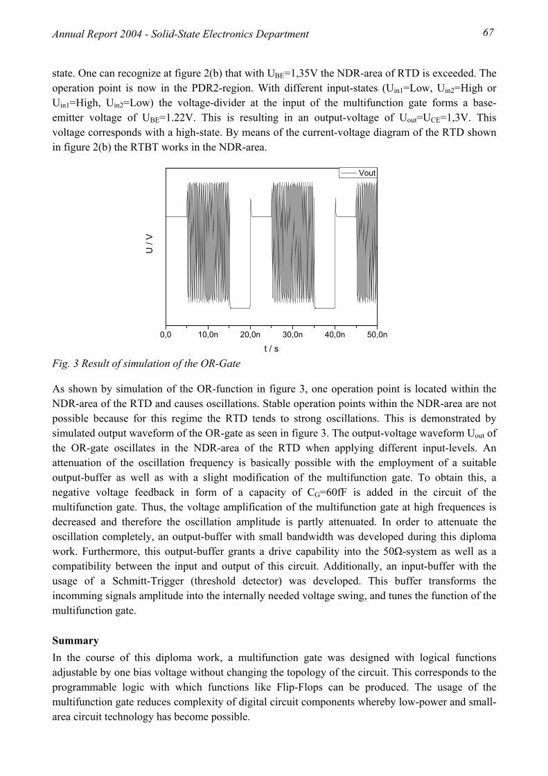
Annual Report 2004 - Solid-State Electronics Department 67
state. One can recognize at figure 2(b) that with UBE=1,35V the NDR-area of RTD is exceeded. The operation point is now in the PDR2-region. With different input-states (Uin1=Low, Uin2=High or Uin1=High, Uin2=Low) the voltage-divider at the input of the multifunction gate forms a base-emitter voltage of UBE=1.22V. This is resulting in an output-voltage of Uout=UCE=1,3V. This voltage corresponds with a high-state. By means of the current-voltage diagram of the RTD shown in figure 2(b) the RTBT works in the NDR-area.
Fig. 3 Result of simulation of the OR-Gate
As shown by simulation of the OR-function in figure 3, one operation point is located within the NDR-area of the RTD and causes oscillations. Stable operation points within the NDR-area are not possible because for this regime the RTD tends to strong oscillations. This is demonstrated by simulated output waveform of the OR-gate as seen in figure 3. The output-voltage waveform Uout of the OR-gate oscillates in the NDR-area of the RTD when applying different input-levels. An attenuation of the oscillation frequency is basically possible with the employment of a suitable output-buffer as well as with a slight modification of the multifunction gate. To obtain this, a negative voltage feedback in form of a capacity of CG=60fF is added in the circuit of the multifunction gate. Thus, the voltage amplification of the multifunction gate at high frequences is decreased and therefore the oscillation amplitude is partly attenuated. In order to attenuate the oscillation completely, an output-buffer with small bandwidth was developed during this diploma work. Furthermore, this output-buffer grants a drive capability into the 50Ω-system as well as a compatibility between the input and output of this circuit. Additionally, an input-buffer with the usage of a Schmitt-Trigger (threshold detector) was developed. This buffer transforms the incomming signals amplitude into the internally needed voltage swing, and tunes the function of the multifunction gate.
Summary In the course of this diploma work, a multifunction gate was designed with logical functions adjustable by one bias voltage without changing the topology of the circuit. This corresponds to the programmable logic with which functions like Flip-Flops can be produced. The usage of the multifunction gate reduces complexity of digital circuit components whereby low-power and small-area circuit technology has become possible.
0,0 10,0n 20,0n 30,0n 40,0n 50,0n
U /
V
t / s
Vout

Annual Report 2004 - Solid-State Electronics Department 68
4.3.5 Boolean Logic Application of Resonant-Tunneling Bipolar-Junction-Transistors
Scientist: A. Matiss, J. Driesen, S. Ehrich
Introduction Resonant tunneling bipolar transistors are simulated and measured respectively for use in digital circuits. A single device connected by a voltage divider with two inputs allow the realization of up to six boolean functions.
Device Description The device used for the simulations and measurements is described in figure 1. The common heterostructure layersystem of a HBT, a resonant tunneling diode (RTD) is inserted in the emitter of a HBT. The two quantum barriers are realized by 4 nm InAlAs layers and the quantum well by a 5 nm InGaAs layer. The quantum structure is directly implemented into the emitter. Thus, the measurement characterization of the device and modelling required a combined model for circuit simulation of HBT and RTD.
n -InGaAs
i-InGaAs C
B
E
n -InGaAs
p+-InGaAs:C
n+- InGaAs
n-InP etch stop
120 nm
600 nm
base
collector
10 nm
300 nmsub-collector
50 nm
25 nmemitter
5 nm
n+-InGaAs emitter-cap 50 nm
etch stop
s.i. - InP:Fe
i-InP
RTD4 nm
4 nm
InAlAs
InAlAs InGaAs
50 nm
B
C
E
RCR1
R2
GND
VIN 1
VIN 2
VCC
VOUT
RTBTB
C
EE
Fig. 1 RTBT layer system Fig. 2 Logical gate design
Logic Application The measurement setup of the logical gate is presented in figure 3. Its two inputs are VIN,1 and VIN,2 connected via a voltage divider to the base of the RTBT. The output voltage VOUT is located between the load resistor RC and the collector of the RTBT. The RTD located in the emitter is connected to ground reference. Due to the voltage divider four different base potentials are possible. For the further investigations, both inputs are assumed to be set with the same VLOW and VHIGH

Annual Report 2004 - Solid-State Electronics Department 69
voltage. This reduces the possible states at the base to three voltages. For certain bias voltages this device outputs in dependence of the input voltage offset and voltage swing up to six different logic functions as presented in figure 5-10 in dependence to the base voltage.
v(t)
DUT
VoutVin1,2
Vcc
RcR1
R2
Vin1 Vin2
Fig. 3 Measurement setup
The three possible voltages are shown in figure 4 for the EOR-function in the tranfer characteristic plot of the RTBT. For the resulting voltages of VB=1.5V, 1.3V and 1.1V The output at the collector becomes either Vout=0.9V or 1.5V, depending on the logical function. The influence of the bias voltage is also displayed. One can change the output offset of the signal by adjusting the VCC voltage.
0.4 0.6 0.8 1.0 1.2 1.4 1.6
0.6
0.8
1.0
1.2
1.4
1.6
1.8
2.0
2.2
2.4
2.6
EOR
III
II
I
2.4Vcc 2.3Vcc 2.2Vcc 2.1Vcc 2.0Vcc 1.9Vcc 1.8Vcc
V OU
T (V
)
VIN (V)
Fig. 4 Transfer characteristic with EOR function operation points

Annual Report 2004 - Solid-State Electronics Department 70
-2us -1us 0us 1us 2us0.60.81.01.21.4
1.01.21.41.6
0.60.81.01.21.41.01.21.41.61.80.60.81.01.21.41.01.21.41.61.8
0.60.81.01.21.4
XNOR
time
Input
AND
NAND
Vol
tage
OR
NOR
XOR
Fig. 5 Input and output waveforms of six boolean functions

Annual Report 2004 - Solid-State Electronics Department 71
4.3.6 Investigation of Self-oscillation of Resonant Tunneling Devices
Scientist: A. Matiss Student: T. Geistert
Introduction Unwanted self-oscillation of resonant tunneling devices can cause distortion in the circuit where the NDR-device is employed. As an initial investigation of realized NDR devices and circuits, the charaterization of the devices instability that occurs for certain DC bias conditions is measured with a spectrum analyzer in a 50Ω environment.
Measurement Setup and Description The measurement setup for a single device characterization is shown in fig. 1. The device under test in this example is connected via bias tees to two DC bias-sources at the input and the output of the device. The RF connector of the input bias tee terminates in a 50 Ω load, while the output RF path leads to a 50 GHz spectrum analyzer with a 50 Ω coaxial RF input. It is also possible to use tunable loads instead of the 50 Ω loads to investigate the devices instability behaviour in dependence of different source and load impedances. The measurement is performed by recording the amplitude of the output power in dBm over a certain frequency span, and sweeping the DC bias of the device. The frequency resolution of the spectral analysis has a crucial influence on the
Fig. 1 Measurement setup for instability characterization of NDR-devices.
accuracy of the sampled data and needs to be adjusted manually. Other necessary predefinitions are made via a LabView software. The program allows an up and down sweep of either VDC1 or VDC2 for an adjustable voltage range. Sweeping both directions at once is recommended because most resonant devices show a non-linear hysteresis in their NDR region. Thus is is necessary to record the output power for the up and downsweep of the voltage to investigate nonlinearities. This measurement setup is also suitable for characterization of voltage controlled oscillators and similar devices in the frequency domain.
SpectrumAnalyzer
VDC2VDC1
Bias Tee
Lfeed Lfeed
CblockCblock
50Ω
DUT

Annual Report 2004 - Solid-State Electronics Department 72
Measurements on resonant tunneling bipolar transistors Common heterostructure bipolartransistors with a resonant tunneling diode in the emitter layer system cause oscillation if the DC operation point is located in the NDR region of the BE-diode. The measurements are made by sweeping the base-emitter voltage and holding the colletor-emitter voltage on a constant level. In this measurement, the NDR region reaches from 1.1V up to 1.3V. In fig. 2 the measured power is plotted over the observed frequency span and the base-emitter voltage. The blue area indicate no oscillations and is associated with the system noise floor of the spectrum analyzer and the measurement setup. The green, yellow, orange and red lines indicate a power peak for certain frequencies and bias voltages. Due to the resonant behaviour of a RTBT, oscillations depending on the source/load impedances will appear if the base-emitter voltage reaches the NDR region. At the borders of the NDR region, oscillations are observed over the whole frequency span. This wide-band noise effect is found for biasing the device at the peak and the valley boundary of the RTD. During the sweep through the negative differential resistance region, one frequency is identified with a high RF-power. Measurements have shown that the investigated RTBT oscillates at high frequencies (~13 GHz) with high output peak power (~8 dBm) presented in fig. 2 for base voltage = 1.2V and collector emitter volatage = 1.5V.
0 5 10 15 20 25 301.10
1.12
1.14
1.16
1.18
1.20
1.22
1.24
1.26
1.28
1.30
Frequency / GHz
Bas
e vo
ltage
/ V
-64 dBm
-56 dBm
-48 dBm
-40 dBm
-32 dBm
-24 dBm
-16 dBm
-8.0 dBm
0 dBm
Fig. 3 Output power-frequency spectrum of NDR region of resonant tunneling device
The second harmonic is found at 26 GHz. But due to the bandwidth limitation of the measurement system of 20 GHz, the measurements above that frequency are considered being inaccurate. A spectrum for a certain bias condition is shown in fig. 3. Here one can find the peaks of the first and second harmonic.

Annual Report 2004 - Solid-State Electronics Department 73
0.0 5.0G 10.0G 15.0G 20.0G 25.0G 30.0G-80
-70
-60
-50
-40
-30
-20
-10
0
Pow
er [d
Bm
]
Frequency [Hz]
Fig. 4 Power spectrum of RTBT for VDC1 = 1.18V

Annual Report 2004 - Solid-State Electronics Department 74
4.3.7 Optical Measurements of MOBILE with CW-Laser
Scientist: A. Matiss, E. Khorenko
Introduction Optoelectronic measurements are performed on an optical receiver circuit formed by combination of pin-diode and monostable bistable logic elements. The optical to electrical conversion of a continuous wave signal is verified at low frequency.
Device description First demonstrators were realised using InP-based devices. We have designed and fabricated a monolithically integrated MOBILE circuit with a pin-diode at the input and an output amplifier based on HFETs. The fabricated pin-diodes have a diameter of 15 or 25 µm depending on the area of the RTDs in the circuit. The realized RTDs have areas between 5-45 µm². The output amplifiers were realized by HFETs with a channel length of 1 µm. The whole layer stack was grown by Metal organic Chemical Vapour Deposition (MOCVD). The layers of the Hetero-Structure-Field-Effect Transistor (HFET) were grown at first on the InP-substrate followed by the layers of the RTD. The pin-diode was grown on top of the RTD-layers resulting in a 1400 nm thick layer stack (see figure 2). The HFET consists of a heavily doped InGaAs contact layer, an i-InGaAs channel and an InP-buffer, which separates the transistor and the substrate. The RTD is made of an InAlAs/InGaAs/InAlAs (5 nm/ 5 nm/ 5 nm) double-barrier structure and n+-InGaAs contact layers. The double-barrier structure and the contact layers are separated by a thin i-InGaAs spacer (3 nm). The pin-diode layers consist of a p-InGaAs contact layer and a 600 nm i-InGaAs absorption layer. To reduce the process steps, the n-contact of the pin-diode nd the anode of the RTD are combined in one layer (n+-InGaAs). The circuit was processed by conventional wet-etching. The layers of the different devices were separated by i-InP etchstop layers to enable selective wet etching.
Measurement Results
Fig. 1 Layer system of circuit concept and MOBILE stage design without amplifier
DG
S
p-InGaAsA
absorptionC A
C
InP-Substrat
HFET
channel
RTD
i-InP-etchstop layer
HFET
PIN-diode
RTDPIN-diode
A: anodeC: cathodeD: drainG: gateS: source
n-InGaAs
A
pin
diod
e
RTDLoad
RTDDriver
differentialamplifier
pin-
diod
e
Vclk
Vpin

Annual Report 2004 - Solid-State Electronics Department 75
Figure 2 depicts the bifurcation curve of the MOBILE in dependence on the incident light on the pin-diode. The MOBILE switches to its second state for photocurrents above Iph = 2.2 mA. This value is determined by comparing the two peak currents of the RTDs. The eye-diagram shows the output voltage for different input photocurrents. The MOBILE switches for clock voltages between Vclk=0.6V to 0.8V.
Fig. 2 Bifurcation curve of the MOBILE with a pin-diode providing various
Optical measurements have been made by employing a continuous wave laser beam to the pin-diode to verify the switching behaviour of the device. The clock voltage has been alternated by a square function to set and reset the MOBILE-states. The figure 3 shows the results for 100 kHz clock frequency.
The next measurement has been performed by altering the clock input and modulating the incident laser beam with 2 Gbit/s. In figure 4 the MOBILE has been testet employing a bit error rate test system suitable for frequencies up to 12.5 Gbit/s. The measured eye-diagram at 2Gbit/s pseudo random binary sequence (PRBS 27-1) shows a good eye-apperture of 50mV for each differential output, and therefore 100mV in the differential function as presented in the upper plot in the figure.
-0.1 0.0 0.1 0.2 0.3 0.4 0.5 0.6 0.7 0.8 0.9 1.0 1.1-0.1
0.0
0.1
0.2
0.3
0.4
0.5
0.6
0.7
Iph=0mA Iph=1mA Iph=2mA Iph=3mA
Out
put /
V
Clock / V
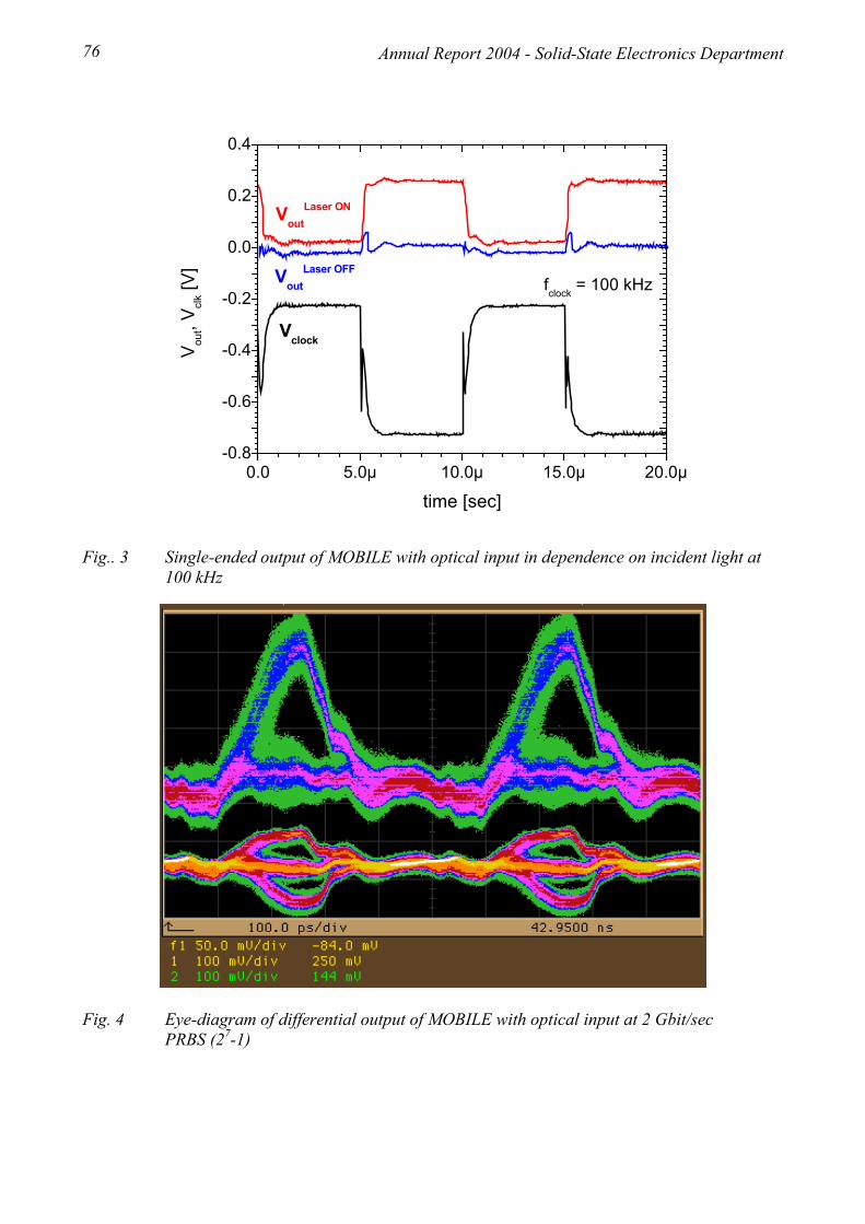
Annual Report 2004 - Solid-State Electronics Department 76
0.0 5.0µ 10.0µ 15.0µ 20.0µ-0.8
-0.6
-0.4
-0.2
0.0
0.2
0.4
fclock = 100 kHz
VoutLaser ON
VoutLaser OFF
Vclock
V out,
V clk [
V]
time [sec]
Fig.. 3 Single-ended output of MOBILE with optical input in dependence on incident light at
100 kHz
Fig. 4 Eye-diagram of differential output of MOBILE with optical input at 2 Gbit/sec PRBS (27-1)

Annual Report 2004 - Solid-State Electronics Department 77
4.4 Nanoelectronics

Annual Report 2004 - Solid-State Electronics Department 78
4.4.1 Photoluminescence Characterisation of GaAs Nano-Whiskers on Si Substrate
Scientist: V. Khorenko Technical Assistant: R. Geitmann
Introduction In the recent years semiconductor nanowhiskers have gained much attention due to their potential application in the design of novel electronic, photonic and sensing devices [1-3]. An additional important feature of structures consists in a possibility to combine highly strained materials without degradation of their crystal structure[4] and, therefore, electronic and optical properties. An essential example of such the combination is growth of III/V-based semiconductor nanowires on Si substrate already demonstrated by several research groups. Further steps towards the succesfull realisation of nanowhisker-based devices and circuits need an investigation of their properties in dependence of the growth and material parameters. In this work we investigated the photoluminescence properties of GaAs nanowhisker grown on Si substrate.
Experimental details For the nanowhisker growth the (111) Si substrates were used. Gold nanoparticles prepared by reduction of HAuCl4 with sodium citrate in an aqueous solution [5] were used as a growth catalyst defining the size and the position of growing whiskers on the substrate. The diameter of the particles deposited ranged from 5 nm to 100 nm. After the nanoparticle deposition, the samples were annealed in the N2 atmosphere at 300°C for 300 seconds in order to remove organic residuals originating from the synthesis process.
The growth was performed in an AIX200 RF low-pressure MOVPE system with a full non-gaseous source configuration. Triethylgallium (TEGa) and tertiarybutilarsine (TBAs) were used as precursors. After annealing the Si wafer at 600 °C under nitrogen and TBAs flow the temperature was reduced to 400 °C. The growth was carried out at a V/III ratio of 5 and a total pressure of 50 mbar, respectively. Additionally, GaAs whiskers on (111) GaAs substrate were grown as a reference in the same run. More details about the growth can be found in the Chapter 4.1 “Epitaxial growth and materials”.
For the photoluminescence measurements the samples were mounted in an closed-cycle cryostat allowing measurements in a temperature range from 15 to 300 K. A Nd:YVO4 laser with an emission line of 532 nm was used as an excitation source. The photoluminescence signal was dispersed by a 0.64-meter focal length Jobin-Yvon monochromator and detected with a GaAs photo-multiplier tube. A standard lock-in signal processing was used to improve the signal-to-noise ratio.

Annual Report 2004 - Solid-State Electronics Department 79
Characterisation results A scanning electron microscope (SEM) micrograph of the grown GaAs nanowhiskers is presented in the Fig.4b, page X (Ingo’s Bericht). The nanowhiskers have a length of about 8 µm and are randomly distributed on the substrate surface with a density of about 108 cm-2. Despite an expected growth direction perpendicular to the substrate surface, no preferential orientation of the whiskers was observed. We attribute this result to the presence of a thin oxide layer and also a carbon contamination on the Si surface. The oxide layer might not be completely removed during the cleaning and annealing procedures or a slight hydrolysis has occurred during the deposition of the catalyst. Additionally, carbon residuals as well as sodium chloride may cover the silicon surface. This contamination effect did not allowed the whiskers to follow the crystal orientation of the substrate as was reported elsewhere [6]. In contrast, the GaAs whiskers on the GaAs substrate grew in the preferential <111> direction. The structures grown on silicon substrate are slightly tapered and mostly straight but some of them have kinks attributed to the formation of stacking faults in the material. This kind of the structure defects is rather typical for nanowhiskers [7].
Photoluminescence measurements were made at T = 20 K to study the optical properties of fabricated nanowhiskers. Fig. 2(left) shows the spectra of GaAs whiskers on (111) Si-substrate in comparison to raw GaAs and Si substrates. The (111) GaAs substrate (a) exhibits a band gap related transition at 821 nm and also impurity peaks around 840 nm and 860 nm. The GaAs nanowhiskers on (111) Si-substrate (b) show an emission around 820 nm. Its intensity is relatively high having the
Fig. 2 Left: photoluminescence of the GaAs-on-Si nanowhiskers (b) and GaAs (a) and Si (c) substrates taken at 20 K. The spectra are vertically shifted for better clarity. Right: photoluminescence of the GaAs-on-Si nanowhiskers for the different excitation power (from 50 mW to 550 mW with a step of 100 mW) measured at 20 K. The inset shows the dependence of the peak intensity on the excitation power.
limited number of nanowhiskers of 108 cm-2 (corresponds to the 1% coverage) in mind. The peak is slightly shifted to a shorter wavelength due to electron and hole quantization that becomes significant at a whisker diameter smaller as 40 nm [6]. The size distribution contributes to the broadening of the emission peak. The spectrum from the Si-substrate taken at a 5 times higher

Annual Report 2004 - Solid-State Electronics Department 80
excitation intensity (550 mW) (c) shows no spectral features which confirms that the whiskers are the solely origin of the peak at 820 nm. The shoulder around 880 nm is related to the sensitivity and noise function of the used detector set-up.
The intensity of the photoluminescence spectra of the GaAs nanowhiskers increases almost linearly with the excitation power (Fig. 2(right)). No saturation effects occur which implies that the emission is not provided by a limited number of impurities but by the host lattice. This result demonstrates that despite a lattice mismatch of 4.1 % between Si and GaAs and some stacking faults defects observed by SEM, there is no significant degradation of the material quality of GaAs whiskers grown on Si.
In summary, we demonstrated the growth of GaAs nanowhiskers grown on (111) Si substrate using catalytic Au nanoparticles. The fabricated whiskers with a length of about 8 µm show a photoluminescence signal attributed to the transitions of the host lattice. The distribution of the whisker diameter did not allow to resolve details of the possible excitonic structure. Further improvement of the optical properties of GaAs nanowhiskers grown on Si substrate should be possible by optimization of the nanoparticle deposition and the growth procedure.
Acknowledgement This work was supported by the Sonderforschungsbereich SFB 445.
References: [1] M.S.Dresselhaus et al., Mater.Sci.Eng., C23, 129 (2003). [2] Y.Xia et.al., Adv.Mater., 15, 353 (2003). [3] C.M.Lieber et al., MRS Bull., 28, 486 (2003). [4] T.Martensson et al., Nano Lett., 4, 1987 (2004). [5] A. Lehnert, Ph.D. Thesis, Universität Essen, (1991). [6] K.Hiruma et al., J. Appl. Phys., 77, 447 (1995). [7] M. T. Björk et al.,Appl. Phys. Lett., 80, 1058 (2002).

Annual Report 2004 - Solid-State Electronics Department 81
4.4.2 Integration of an Aerosol Generator in the MBE
Scientist: V. Khorenko, Technical Assistant: R. Geitmann, in cooperation with E. Kruis and C. Kleinert (Process and Aerosol Measurement Technology Department)
Introduction A prerequisite for synthesis of novel nanostructured materials is the technology development. Modern needs in highest control level over all the fabrication process parameters and growing interest in non-traditional material combinations exceed often the limits of conventional technologies. We develop a novel approach to fabricate zero-dimensional nanostructures (quantum dots) allowing to control their size and surface density, as well as to use a wide range of materials from isolators to metals. This approach employs the generation of nanoparticles in the gas phase [1] with subsequent embedding in a host matrix by semiconductor epitaxy [2].
As a model system, we chosen Indium nanoparticles which are to be modified to InAs and embedded in GaAs. Owing to the nanometer size the particles have got a very large surface/volume ratio and are very sensitive to the oxidation. Data of transmission electron microscopy (TEM) and x-ray photoelectron spectroscopy (XPS) clearly show the formation of a thin oxide layer on the nanoparticle surface after the expostion to air (Fig.1). The thickness of this layer of just few nanometer is enough to avoid the conversion of In in In(Ga)As during the overgrowth with GaAs.
Fig. 1 Left: STEM micrograph of a gas-phase generated In nanoparticle exposed to air; Right: XPS spectra of In3d5/2 and In3d3/2 electrons of In nanoparticles (a) on the particle surface (b) after removing ~2 nm thick oxide layer. (Courtesy of B. Balamurugan and E.Krius)
440 445 450 455
In 3
d 3/2
In 3
d 5/2
In2O
3
In
(b)
(a)
XPS
Inte
nsity
(arb
. uni
ts)
Binding Energy (eV)
20 nm

Annual Report 2004 - Solid-State Electronics Department 82
Presented result clearly shows a necessity of a combined technology without a sample transfer after the nanoparticle deposition to the epitaxy chamber through the air. We modified the nanoparticles deposition set-up (aerosol generator) and developed a deposition chamber (so-called electrostatic precipitator, ESP) which is compatible with requirements of a molecular beam epitaxy machine.
Developed set-up An essential technical problem that appeared in realisation of the concept “MBE with integrated aerosol generator” was totally different working pressures in both the machines. Nanoparticle synthesis in the gas phase needs the atmospheric pressure, whereas molecular beam epitaxy is based on ultra high vacuum environment conditions. This difference makes the direct deposition of nanoparticles in the growth chamber of MBE impossible and, therefore, the aerosol generator has to be used as an additional chamber within MBE system only. We redesigned the ESP according to mechanical and vacuum standards of the MBE. In a pump-down test a pressure of <10-7 mbar was be achieved. The ESP was equipped with a rail system for the sample transfer and then mounted on the “free” end of the MBE’s transfer chamber. A separate pump system with a cryogenic pump was used to evacuate the ESP chamber before and after the deposition process so, that the sample transfer take place in vacuum environment only.
Fig 2. A picture of the aerosol generator integrated into the MBE: 1 – ESP, 2 – transfer chamber, 3 – growth chamber of the MBE machine, 4 – cryogenic pump, 5, 7 – furnaces of aerosol generator, 6 – differential mobility analyser
In order to exclude the oxidation of Indium during the synthesis and the deposition of nanoparticles completely, we used high quality nitrogen gas (>99.(6N)%) as a carrier gas. The carrier gas provides the nanoparticle transport through the set-up to the deposition chamber. In order to control the gas flow in the system two mass-flow controller were implemented.
First tests with annealing of deposited nanoparticles in the growth chamber of the MBE showed a significant difference between the nanoparticles transferred through air and these one’s prepared in

Annual Report 2004 - Solid-State Electronics Department 83
the modified set-up. Because indium oxide In2O3 is a very stable substance with the melting point at ~1900°C, a thin oxide layer on the surface of In is enough to prevent the run of nanoparticles on the surface even at 600°C. The particles prepared in the modified set-up do not have an oxide “skin” and therefore run on the surface during temperature treatment (Fig.3 right). Annealing with As2 overpressure conserves the form of nanoparticles (Fig.3 left) due to, as we expect, conversion of In in InAs. In order to obtain a detailed information about the structure and chemical composition of nanoparticles annealed with As2 overpressure a series of structure characterisation by TEM and EDX is planned as a next step towards the synthesis of nanoparticle-based InAs quantum dots in GaAs matrix.
Fig.3 AFM micrograph of In nanoparticles on GaAs substrate annealed at 600°C with (left) and without (right) As2 overpressure.
Acknowledgement This work is supported by Sonderforschungsbereich SFB445 “Nanoparticles from the gas-phase”
References: [1] F.Kruis et al, „Preparation of sizeclassified PbS nanoparticles in the gas-phase“, Applied Physics
Letters v.73, n.4 pp547-549 (1998).
[2] M.A.Herman, H.Sitter, “Molecular Beam Epitaxy: Fundamentals and Current Status”, Springer Verlag, ISBN 3540605940, 1997

Annual Report 2004 - Solid-State Electronics Department 84
4.4.3 Selfgating Effect in a Novel Nanometer-Scale Semiconductor Device Utilizing an Asymmetric 2-DEG Channel
Scientist: Q. T. Do T.Müller1, A. Lorke1 Technical Assistant: R. Geitmann 1 University Duisburg-Essen, Solid State Physics Dept., Lotharstr.1, D-47048 Duisburg, Germany
Introduction We report on a novel III-V semiconductor device utilizing a self-gating mechanism for non-linear carrier transport in a narrow conductive channel. This so-called self-switching device (SSD) was fabricated from an InGaAs/InAlAs/InP semiconductor heterostructure by electron beam lithography and subsequent wet-chemical etching. Current-voltage measurements both at room temperature (RT) and at low temperatures (LT) down to 240 mK reveal a diode-like output characteristic. Exploiting the inherently lateral current control mechanism, the device is extended to field-effect-transistor (FET) by a side gate structure. By using an equivalent circuit model, we are able to describe the basic working principle [1].
For the fabrication of the SSD [2], a MBE-grown high mobility In0.53Ga0.47As/In0.52Al0.48As/InP two-dimensional electron-gas (2DEG) heterostructure (RT electron concentration: 3.7·1012 cm-2, RT mobility 8958 cm2/Vs) is used. The two-dimensional electron-gas system is confined at an In0.53Ga0.47As/In0.52Al0.48As hetero-interface, only 36 nm below the surface of the sample. The mesa and ohmic contacts are defined by conventional UV photo lithography. Thereafter the geometry of our device is patterned using high- resolution electron beam lithography and subsequent wet-chemical etching.
Fig. 1 Atomic force micrograph of a SSD.
source
drain d=~150nm
l=~3000nm
gate

Annual Report 2004 - Solid-State Electronics Department 85
Fig. 2 Output characteristics from the SSD at room temperature.
Figure 1 shows an AFM image of a SSD after processing. The one micron wide channel is narrowed to about 150 nm at the apex of a triangular-shaped constriction. Applying a negative voltage to the upper side of the U-shaped channel, the current inside the narrow region of the channel will be completely pinched-off as a result of the electrostatic field effect from the opposite triangular part of the system. For a positive source-drain voltage the maximum current depends on the channel width at the apex only.
Fig. 3 Output characteristics from the SSD at 240 mK.
-3 -2 -1 0 1 2 3
-6,0µ
-4,0µ
-2,0µ
0,0
2,0µ
4,0µ
6,0µ
8,0µ
10,0µ
UG=-8V UG=-6V UG=-4V UG=-2V UG=0V UG=+2V UG=+4V UG=+8V
sour
ce-d
rain
cur
rent
[A]
source-drain voltage USD [V]
room temperature
area of low resistance
rectification effect
-3 -2 -1 0 1 2 3-500,0n
0,0
500,0n
1,0µ
1,5µ
2,0µ
2,5µ
3,0µ
3,5µ
4,0µ
4,5µ
sour
ce-d
rain
cur
rent
I SD [A
]
source-drain voltage USD [V]
UG=-10V UG=-9V UG=-8V UG=-7V UG=-6V UG=-5V UG=-4V UG=-3V UG=-2V UG=-1V UG=0V UG=+1V UG=+2V
@ 240mK

Annual Report 2004 - Solid-State Electronics Department 86
Fig. 4 Equivalent circuit model for the SSD.
This device can be further fine-tuned by applying an additional side-gate voltage to the lower contact in order to control the conductance of channel. Using this additional side-gate, the onset source-drain voltage is defined by either the channel geometry or the applied side-gate voltage. Figures 2 and 3 show the output characteristics from our device at room temperature and 240 mK respectively. The traces are recorded at different side-gate voltages. The output characteristics derived from an FET like equivalent circuit model (fig.4) for the SSD are shown in figure 5. Most of the features from our measurements (such as the diode-like characteristic and the shifting onset voltage) are qualitatively well reproduced.
Fig. 5 Simulated output characteristics of the SSD.
References: [1] Q. T. Do, T. Müller, A. Lorke, F.-J. Tegude, Nanoelectronics Day, Jülich, 2005. [2] A.M. Song and M. Missous, Unidirectional electron flow in a nanometer-scale semiconductor channel: A self-switching device, Appl. Phys. Lett., Vol.83 1881 (2003).
-3 -2 -1 0 1 2 3-2,0µ
0,0
2,0µ
4,0µ
6,0µ
8,0µ
10,0µ
UG=-3.0V UG=-2.5V UG=-2.0V UG=-1.5V UG=-1.0V UG=-0.5V UG=0V
sour
ce-d
rain
cur
rent
I SD [A
]
source-drain voltage USD [V]
simulated output characteristics

Annual Report 2004 - Solid-State Electronics Department 87
4.4.4 Enhancement of an Scanning Force Microscope for I/V-Measurement on Nanoelectronic components
Student: H.G. Kreusch Supervisor: Q.T. Do, W. Prost
Introduction Since the invention of scanning probe techniques like the Scanning Tunneling Microscope (STM) and the Scanning Force Microscope (SFM) in the 1980’th a lot of progress was achieved for the development of various applications at ultra high resolution. The availability of conductive tips makes it possible to use the SFM as a Conductiv-SFM (C-SFM) for current-voltage-measurements applied to nanostrcutured and nanoelectronic components aiming at below 100 nm lateral resolution. The topic of this work is to enhance the functionality of a Dimension 3000 SFM to a C-SFM, while all other functions are kept in normal operation.
Hardware solution For I-V meausrements a separate wire was soldered at the tipholder of the DI 3000 in order get an electric contact to the tip. The tip holder is compatible to standard silicon tips and a highly conductive connection to the tip is achieved. There are mainly two different types of conductiv tips, i.e. highly doped diamond coated and metal coated tips. The diamond coated tips usually were 1 x 1021 cm-3 boron doped with a radius of about 100 nm and coating thickness of 100 nm. For safe operation at 1 µN contact force a maximum current of 10 µA should not be exceeded. Otherwise thermal damage will occur. Many sorts of metal coatings were available. Because of the physical stress, coatings out of tungsten carbide or titanium nitride give the best results. The coatings were about 20 nm thick and the tip radii were about 20 nm. Because of their lower tip radius a maximum current of 1 µA at 1 µN contactforce was tested for safe operation.
In Figure 1 the Dimension 3000 is shown along with the extentions for I-V measurements. A Source-Measure Unit (SMU) and a computer with GPIB card were added to the workstation for the automation of the measurements. A control unit (see Fig.1b) was constructed and built providing an easy access to the sample (DUT) and the tip. The unit is designed to prevent electrostatic damage and to shield the signals. The control unit includes four relays which are controlable via SMU 2400 and freely available to the user. Because of 4-wire-measurement-technics no calibration of the equipment is needed. The used guard minimized the leakage of the wire to the tip and the time constant due to the wire capacitance. This way high probe resistance of up to some 10 GΩ can be detected in an aceeptable period of time. Because of its good results in measuring low level voltages and currents and some useful features a Keithley 2400 SMU was used.
A 28 pin chip carrier (JLCC) is used to mount and to bond the sample (DUT). The socket is mounted upon a carrier, deposited and fixed on the SFM chuck. This way several wired connections can be used to supply the DUT. The carrier is isolated against the chuck in allow grounded or isolated I-V measurements. The quantity of the connections to the DUT and to the tip provide multi wire measurement modes. In Fig.1d the scheme of the main parasitic elements affecting the results

Annual Report 2004 - Solid-State Electronics Department 88
of C-SFM measurement are shown. The total isolation resistance is composed of the isolation resistance of the source of 1 TΩ, the resistance between source line and grounf of 80 GΩ, and the isolation between bonded contact pad and ground of 27 GΩ.
Figure 1. C-SFM based on a DI Dimension 3000
Control Software HP-VEE was used to perform the automated I-V measurements. The programme uses a 4-quadrant operation of the SMU 2400 to sweep the voltage and assure easy user access to prepare the parameters for I/V measurement. Some usefull functions were added, such as compliance, sweep step size, varying accuracy vs. time, and the configuration of the 4-wire measurement mode via the control unit.
To control the SFM some standard modes were adapted. Programming a special macro to simplify the control of the SFM failed because the SFM is driven by protected software. Therefore, measurements with SFM laser switched-off are not possible. The Tapping Mode shows best results by searching the destinated testpoint. The implemented “Zoom In” function simplifies targeting. The contact mode with special parameter sets is used to contact tip and sample at the desired testpoint. The spring constant (k) is a characteristic of the tip. The sensitivity, which is one of the parameters, can be determined using the force calibration mode (force plot). Then the contact force

Annual Report 2004 - Solid-State Electronics Department 89
can be approximated by knowing the vertical deflection and choosing the setpoint, in use of equation 1.
[ ] [ ] [ ]( ) = − N
N nmF nN k * Sensitivity * Setpoint V vert.def. V ( equation1 )m V
Verification measurements To proof the capability of the measurement system, electrical conductivity measurements on Gold-Nanoparticle Coated Cristals (Au-NCC’s) and Nano-Whisker were conducted. Both were nanometric sized, so they were not directly contactable by using a wafer prober. Two types of Au-NCC’s were tested, i.e. Au-K2SO4-NCC’s and Au-Pd-RbSO4-NCC’s. The geometric values of the tested Au-NCC’s stray in between the ranges: 100 nm < L,D < 4000 nm; 50 nm < H < 200 nm. The Nano-Whisker were grown ( MOVPE ) on 1x1018 cm-3 tin doped indium arsenide substrate. Their radii were approximatly 50 nm and 100 nm at 800 nm to 1000 nm height.
-4
-2
0
2
4
6
-6
-4
-2
0
2
4
6
-0.4 0.0 0.2 0.4
-4
-2
0
2
4
6
FN = 1 µN
InAs-Whisker_1
Cur
rent
[µA
]
Voltage [V]
InAs-Whisker_2
InAs-Substrate
-0.2
Fig. 3 Current-Voltage characteristics for two InAs-Wiskers.
Assuming the scheme in Fig.1d with Nano-Whiskers as DUT’s the main circuit elements affecting the results of C-SFM measurement on Nano-Whisker is given. The resistance of the NCC was found to exceed the total isolation resistance of 27 GΩ. During the verification a conductivity of two Nano-Whiskers with different dimensions could be demonstrated. Due to a nonlinear resistance graph an approximation of the resistance at low level arround the origin was made. It leads to 130 kΩ resistivity once and to 400 kΩ resistivity for the other Whisker[3].
References: [1] H.G. Kreusch: Erweiterung eines Rasterkraftmikroskops zur Aufnahme von I/U-Messungen
an nanoelektronischen Bauteilen, Diploma thesis at HLT in August 2004, Universität Duisburg-Essen
[2] K.D.Katzer, W.Mertin, G.Bacher: Conductivity measurements on single NCC´s Escher Technical Report 2003-2004, Universität Duisburg-Essen
[3] cf this report, chapter 4.1.4

Annual Report 2004 - Solid-State Electronics Department 90
4.4.5 Probing Carriers in Low-dimensional Systems with High Spatial Resolution by Novel Scanning Probe Techniques
Student: S. Bonsels Supervisor: S. Anand, O. Douheret, KTH Stockholm
Preface This work has been carried out as a study internship at the Royal Institute of Technology (KTH) Stockholm.
Introduction In this report, cross-sectional scanning capacitance microscopy (SCM) and scanning spreading resistance microscopy (SSRM) are used to characterise and to image samples at high spatial resolution. The investigated structures consist of double quantum well (QW) structures with different inter-well spacing. The spatial resolution is defined as the lowest QWs distance from which the two capacitance or resistance dips can be resolved. Sub 25 nm and sub 5 nm spatial resolution are reported for SCM and SSRM, respectively, using commercial probes. Additionally a quantum dot (QD) structure has also been investigated with SSRM and detection at the atomic scale was able to observe. SCM and SSRM have proven to be powerful techniques for high-resolution electrical characterization of semiconductor materials and devices [1]. Advantages with these methods include, high sensitivity to doping variations, wide dynamic range (1015-1020cm-3), and especially high spatial resolution, and further more for SCM due to the relatively low contact forces in AFM contact mode a non-destructive behaviour [2]. However, in both techniques the spatial resolution has been shown to be tremendously dependent of many experimental parameters, such as the forces employed, voltage biases applied, and especially the tip geometry. Due to the inherent sensitivity to carries, the variation of the SCM and SSRM contrast at homojunctions is spatially expanded typically in the order of the Debye length [3]. This hampers the determination of the spatial resolution and stresses the requirements of interfaces with abrupt variations of carriers. Due to the abrupt variations of carriers at heterojunctions, QW structures are suitable to evaluate SCM and SSRM spatial resolution.
Experimental Two In0.53Ga0.47As/InP (lattice matched) QW samples grown by MOVPE on n+-InP substrate were investigated. In sample A, the QW widths were 10 nm and in sample B, 5 nm. Both samples consisted of five sets of two identical QWs and different inter-well spacing: 10 nm (set 1), 20 nm (set 2), 50 nm (set 3), 100 nm (set 4), and 200 nm (set 5). The InP barriers and the inter-well spacing were n-doped (1×1017cm-3) and Si was used as the dopant. Commercial metal (PtIr5) coated and B-diamond coated etched silicon tips (Nanosensors GmbH) were used in SCM and SSRM, respectively. Finally, the present investigations, both SCM and SSRM profiles are obtained by image averaging. The sample of the QD structure consists of 5 layers of In0.53Ga0.47As QDs separated by 50 nm of GaAs-barriers. The QDs are randomly distributed on thin wetting layers that are a result from the growth (Stranski-Krastanow growth method). The GaAs-barriers and the QDs are unintentionally doped and sandwiched between two highly Si doped GaAs contact layers.

Annual Report 2004 - Solid-State Electronics Department 91
Scanning capacitance microscopy spatial resolution Fig. 1 presents the whole structure of sample A and B scanned by SCM. The characteristic dips are observed at the locations of the QWs consistently with the high carrier accumulation. The peaks surrounding the dips correspond to the depletion region. Exclusively for set 5 the two QWs could be independently resolved, with a SCM dC/dV signal from the interval spacing layer dropping almost down to the barrier level signal. Significant averaging effect due to the overlapping of the depletion regions are progressively evidenced reducing the interwell spacing. The two characteristic dips could however be observed from the set 3. In the case of set 2 and set 1 the measurements indicate that we are towards the resolution limit considering that the two QWs are barely distinguished. Using smaller scan sizes to improve the resolution of the measurement indicate a spatial resolution around 25 nm. This experimental value is in good agreement with simulation results of SCM. Using different parameters the best fit between experimental results and simulation was obtained for a tip radius of 25 nm.
500 1000 1500 2000 2500
depletion region QWQW
set5set4set3set2set1
10 nm QW structure 5 nm QW structure
dC/d
V
distance (nm)
Fig. 1 Complete SCM dC/dV profiles of sample A and B. Dc bias and ac bias were set to 0,8V and 2V, respectively.
Scanning spreading resistance microscopy spatial resolution Fig. 2 shows typical SSRM profile of sample A and B and includes all the wells (set 1 to 5). Characteristic dips are observed at the location of the QWs consistent with the high carrier accumulation. The observed dips for the 10 nm QW structure are, as expected, wider than for the 5 nm QW structure. Like in SCM, smaller scan size was then used and for each set the two QWs were able to be independently resolved. This clearly underlines a spatial resolution below 15 nm. The lowest inter-well spacing from which the two wells can be resolved was then reached by extrapolation. This result indicates that the spatial resolution of SSRM is between 2.5 nm and 5.5 nm.
Scanning spreading resistance microscopy characterisation of InGaAs/GaAs QDs As expected, the GaAs-barrier layers exhibit a lower spreading current compared to the highly n-doped GaAs layers. In the recorded image five bright lines 50 nm apart from one another can be observed and correspond to the InGaAs wetting layers. The thickness of the wetting layer is known to lie typically around 1 nm. Along the wetting layers small clear bright spots irregularly distributed and indicate the QDs.

Annual Report 2004 - Solid-State Electronics Department 92
0 250 500 750 1000 1250 1500 1750 2000 2250
QWQW
10 nm QW structure 5 nm QW structure
set5set4set3set1 set2
Res
ista
nce
(Ω)
distance (nm) Fig. 2 Complete SSRM profiles of samples A and B. Dc bias were set to 0,5V.
0 100 200 300 400 500 600
(a)
(b)
effect of a quantum dot
distance (nm)
curre
nt (a
. u.)
effect of the wetting layers
Fig. 3 Spreading current (a) and (b) profile of the quantum dots sample. Measurements were
performed for a dc bias voltage of 2V.
Acknowlegments Thanks to the whole group of materials and semiconductor physics at the Royal Institue of Technology of Stockholm, KTH and specially S. Anand and O. Douhéret.
References [1] International Technology Roadmap for Semiconductor, http://public.itrs.net/, 2003 Edition of the
ITRS [2] G. Binnig, C. F. Quate and Ch. Gerber, Phys. Rev. Lett. 56, 930-934 (1986) [3] C. C. Williams, Annual Revue of Material Science 29, 471 (1999)

Annual Report 2004 - Solid-State Electronics Department 93
4.5 Conference Contributions
1. N.V.ALKEEV1, P.VELLING2, E.KHORENKO, W.PROST, F.J.TEGUDE 1: Inst. of Radioengineering & electronics, Russioan Academy of Sciences, Moscow, Russia 2: IPAG-Innovative Processing AG, Duisburg
Resonant tunneling diode impedance dependence analysis 'The Fifth International Kharkov Symposium on Physics and Engineering of Microwaves, Millimeter, and Submillimeter Waves', 2004
2. E.KHORENKO, S.EHRICH, W.PROST, F.J.TEGUDE
Tunnelling Diodes for Compact Very High Speed Circuits 'Third Joint Symposium on Opto- and Microelectronic Devices and Circuits', Wuhan, China March 21-30, 2004
3. V.KHORENKO, A.C.MOFOR1, A.BAKIN1, S.NEUMANN, A.GUTTZEIT1, H.H.WEHMANN1, W.PROST, A.SCHLACHETZKI1, F.J.TEGUDE
1: Technical University Braunschweig, Inst. of Semiconductor Technology Braunschweig, Gernany
Buffer Optimization for InP-on-Si (001) Quasi-Substrates '16th InP & Related Materials Conference' (IPRM 2004), Kagoshima City, Japan, May 31 to June 4, 2004
4. Q.T.DO, K.KATZER1, J.L.MARTINEZ-ALBERTOS2, V.KHORENKO, W.MERTIN1, W.PROST, B.MOORE2, F.J.TEGUDE
1: Dept. of Materials for Electrical Engineering, Gerhard-Mercator University Duisburg 2: University of Strahclyde, Dept. of P&A Chemistry, Glasgow, U.K.
A Nanoparticle-coated Nanocrystal-Gate for an InP-based Heterostructure Field-Effect Transistor '16th InP & Related Materials Conference' (IPRM 2004), Kagoshima City, Japan, May 31 to June 4, 2004
5. S.NEUMANN, P.VELLING, W.PROST, F.J.TEGUDE
Growth and Characterization of InAlP/InGaAs Double Barriers RTDs '12th Metal Organic Vapor Phase Epitaxy' (ICMOVPE XII), May 30-June 4 2004.
6. S.NEUMANN, S.TOPALOGLU, J.DRIESEN, Z.JIN, W.PROST, F.J.TEGUDE
Study of ohmic contacts and interface layers of carbon doped GaAsSb/InP heterostructures for DHBT application '12th Metal Organic Vapor Phase Epitaxy' (ICMOVPE XII), May 30-June 4 2004
7. S.EHRICH, J.DRIESEN, S.NEUMANN, S.TOPALOGLU, W.BROCKERHOFF, F.J.TEGUDE
Investigation of the rf-noise behaviour of InP based DHBT with InGaAs base and GaAsSb base 'Noise in Devices and Circuits', Maspalomas, Spain, 26.-28.05.04

94 Annual Report 2004 - Solid-State Electronics Department
8. A.MATISS, G.JANSSEN1, R.M.BERTENBURG1, W.BROCKERHOFF, F.J.TEGUDE 1: IPAG-Innovative Processing AG, Duisburg
Optical Sensitivity of a Monolithic Integrated InP PIN-HEMT-HBT Transimpedance Amplifier 'European Microwave Week', (EuMW/GAAS 2004), October 11-15, 2004
9. E.KHORENKO, W.PROST, F.-J.TEGUDE, M.STOFFEL1 , R.DUSCHL1 , M.W.DASHIELL1, O.G.SCHMIDT1, G.KLIMECK2
1: Max-Planck-Institut für Festkörperforschung, Stuttgart, Germany 2: School of Electrical and Computer Engineering, Purdue-University, West Lafayette, IN, USA
Manufacturability and Electrical Characteristics of Si/SiGe Interband Tunneling Diodes 'Fifth Int. Conf. on Advanced Semiconductor Devices and Microsystems' (ASDAM '04), 17.-21.10.04, Smolenice, Slovakia
10. I. REGOLIN, V. KHORENKO, S. NEUMANN, H. WIGGERS, F.-J. TEGUDE, W. PROST,
Wachstum von III/V Nano-Whiskern auf Silizium-Substraten 19. Workshop des DGKK-Arbeitskreises "Epitaxie von III/V Halbleitern" Freiburg, 9./10. December 2004
11. V. KHORENKO, A.C. MOFOR, A. BAKIN, A. GUTTZEIT, H.-H. WEHMANN, E.KHORENKO, W. PROST, A. SCHLACHETZKI AND F.-J. TEGUDE, „
Growth of InGaAs/InAlAs resonant-tunnelling diodes on InP-on-Si (001) quasi-substrate German MBE Workshop, Braunschweig, Germany, 11.-12. October 2004
12. H.-H. WEHMANN, A. GUTTZEIT, C. ACHIMESCU, A. BAKIN, A. MOFOR, V.KHORENKO, S.NEUMANN, W. PROST, A. WAAG, A. SCHLACHETZKI UND F.-J. TEGUDE,
III/V-auf-Silizium – eine Möglichkeit für die Nach-CMOS-Zeit? 9th Augustusburg Conf. of Advanced Science (ACAS 20049 - Das Silicium-Zeitalter: Silicium für Mikroelektronik, Photovoltaik und Photonik, 23. - 25. Sept. 2004
13. V. KHORENKO, S. NEUMANN, I. REGOLIN, W. PROST AND F.-J. TEGUDE,
Photoluminescence of GaAs Nanowhiskers Grown on Si Substrate (Poster), Satellite Workshop “Nanoparticles: Synthesis, Characterisation and Properties”, Duisburg, Germany, June 25-26, 2004.
14. K.-D. KATZER1, W. MERTIN1, G. BACHER1, V. KHORENKO, Q.T. DO, F.J.TEGUDE, W.PROST, J.-L. MARTINEZ-ALBERTOS, B.D. MOORE,
1: Dept. of Materials for Electrical Engineering, University Duisburg-Essen
Conductivity measurements on self-assembled nanoparticle coated crystals via a conductive-atomic force microscope, (Vortag), Proc. of 7th International Conference on Nanostructured Materials NANO 2004, 20.-24. June 2004, Wiesbaden, p.67

Annual Report 2004 - Solid-State Electronics Department 95
4.6 Publications
1. E.KHORENKO, S.EHRICH, W.PROST, F.J.TEGUDE
Tunneling Diodes for Compact High Speed Circuits Proc. of '3rd Joint Symposium on Opto- and Microelectronic Devices and Circuits', Wuhan, China, 21.-30.05.04
2. W.PROST;
Disziplin im Nano-Maßstab, Forum Forschung '04, Universität Duisburg-Essen, Duisburg, 2004
3. F.SCHULZE-KRAASCH1, P.VELLING2, W.PROST 1: Dept. of Materials for Electrical Engineering, Gerhard-Mercator University Duisburg 2: IPAG-Innovative Processing AG, Duisburg
Characterisation of ultra-thin III/V-heterostructures by Convergent-Beam-Electron- and High-Resolution-X-Ray Diffraction Mat. Sci. & Eng. B 110, no. 2, 2004, pp. 161-167
4. N.V.ALKEEV1, P.VELLING2, E.KHORENKO, W.PROST, F.J.TEGUDE 1: Inst. of Radioengineering & Electronics, Russian Academy of Sciences, Moscow, Russia 2: IPAG-Innovative Processing AG, Duisburg
Resonant tunneling diode impedance dependence analysis Proc. of 'The Fifth International Kharkov Symposium on Physics and Engineering of Microwaves, Millimeter, and Submillimeter Waves' (IEEE Cat. No.04EX828) Vol.2, 2004, pp.566-568,
5. Z.JIN, S.NEUMANN, W.PROST, F.J.TEGUDE
Sulfur and low-temperature SiNx passivation of self-aligned graded- base InGaAs/InP heterostructure bipolar transistors J Vacuum Science & Techn. B, vol.22, no.3, 2004, pp.1060-1066,
6. Z.JIN, W.PROST, S.NEUMANN, F.J.TEGUDE
Current transport mechanisms and their effects on the performances of InP-based double heterojunction bipolar transistors with different base structures Appl. Phys. Lett. 84(15) 2004, pp.2910- 2912
7. V.KHORENKO, A.C.MOFOR1, A.BAKIN1, S.NEUMANN, A.GUTTZEIT1, H.H.WEHMANN1, W.PROST, A.SCHLACHETZKI1, F.J.TEGUDE
1: Technical University Braunschweig, Inst. of Semiconductor Technology Braunschweig, Gernany
Buffer Optimization for InP-on-Si (001) Quasi-Substrates Proc. of '16th InP & Related Materials Conference' (IPRM 04), Kagoshima City, Japan, May 31 to June 4, 2004

96 Annual Report 2004 - Solid-State Electronics Department
8. Q.T.DO, K.KATZER1, J.L.MARTINEZ-ALBERTOS2, V.KHORENKO, W.MERTIN1, W.PROST, B.MOORE2, F.J.TEGUDE
1: Dept. of Materials for Electrical Engineering, Gerhard-Mercator University Duisburg 2: University of Strathclyde, Dept. of P&A Chemistry, Glasgow, U.K.
A Nanoparticle-coated Nanocrystal-Gate for an InP-based Heterostructure Field-Effect Transistor, Proc. of '16th InP & Related Materials Conference' (IPRM 04), Kagoshima City, Japan, May 31 to June 4, 2004
9. N.V.ALKEEV1, V.E.LUBCHENKO1, P.VELLING, E.KHORENKO, W.PROST, F.J.TEGUDE 1: Inst. of Radioengineering & electronics, Russioan Academy of Sciences, Moscow, Russia
An equivalent circuit model of InGaAs/InAlAs-based resonant tunneling diode for millimetre wave range Radioengineering and Electronics 49(5), 2004, pp.1-7, (in Russian)
10. Z.JIN, S.NEUMANN, W.PROST, F.J.TEGUDE
Effects of (NH4)2S passivation on the performance of graded-base InGaAs/InP HBTs, phys. stat. sol. (a) 201, No. 5, 2004, pp. 1017–1021
11. Z.JIN, S.NEUMANN, W.PROST, F.J.TEGUDE
Surface recombination mechanism in graded-base InGaAs-InP HBTs, IEEE Trans. Electron Devices vol.51, no.6, 2004, pp.1044-1045,
12. Z.JIN, W.PROST, S.NEUMANN, F.J.TEGUDE
Comparison of the passivation effects on self- and non-self-aligned InP/InGaAs/InP double heterostructure bipolar transistors by low- temperature deposited SiNx, J Appl. Phys., 96(1), 2004, pp. 777- 783,
13. Z.JIN, F.OTTEN1, T.REIMANN, S.NEUMANN, W.PROST, F.J.TEGUDE
Current gain increase by SiNx passivation in self-aligned InGaAs/InP heterostructure bipolar transistor with compositionally graded base Solid-State Electronics 48, 2004, pp. 1637–1641
14. S.NEUMANN, P.VELLING, W.PROST, F.J.TEGUDE
Growth and Characterization of InAlP/InGaAs Double Barriers RTDs Proc. of '12th Metal Organic Vapor Phase Epitaxy' (ICMOVPE XII), May 30-June 4 2004 J of Chrystal Growth 272, 2004, pp. 555-558
15. S.NEUMANN, S.TOPALOGLU, J.DRIESEN, Z.JIN, W.PROST, F.J.TEGUDE
Study of ohmic contacts and interface layers of carbon doped GaAsSb/InP heterostructures for DHBT application, Proc. of '12th Metal Organic Vapor Phase Epitaxy' (ICMOVPE XII), May 30-June 4 2004
16. S.EHRICH, J.DRIESEN, S.NEUMANN, S.TOPALOGLU, W.BROCKERHOFF, F.J.TEGUDE
Investigation of the rf-noise behaviour of InP based DHBT with InGaAs base and GaAsSb base Proc. of 'Noise in Devices and Circuits', Maspalomas, Spain, 26.-28.05.04, pp. 470

Annual Report 2004 - Solid-State Electronics Department 97
17. A.MATISS, G.JANSSEN1, R.M.BERTENBURG1, W.BROCKERHOFF, F.J.TEGUDE 1: IPAG-Innovative Processing AG, Duisburg
Optical Sensitivity of a Monolithic Integrated InP PIN-HEMT-HBT Transimpedance Amplifier Proc. of 'European Microwave Week', (EuMW/GAAS 2004), October 11-15, 2004
18. E.KHORENKO, W.PROST, F.J.TEGUDE, M.STOFFEL1, R.DUSCHL1, M.W.DASHIELL1, O.G.SCHMIDT1
1: Max-Planck-Institut für Festkörperforschung, Stuttgart, Germany
Influence of layer structure on the current-voltage characteristics of Si/SiGe interband tunnelling diodes, J. Appl. Phys., Vol. 96, No.7, Oct. 2004, pp.3848-3851
19. V.KHORENKO, I.REGOLIN, S.NEUMANN, W.PROST, F.J.TEGUDE, H.WIGGERS1 1: Inst. of Combustion and Gasdynamics, University of Duisburg-Essen, Duisburg, Germany
Photoluminescence of GaAs nanowhiskers grown on Si substrate, Applied Physics Letters, Vol. 85, No. 26, 2004, pp. 6407-6408
20. E.KHORENKO, W.PROST, F.-J.TEGUDE, M.STOFFEL1 , R.DUSCHL1 , M.W.DASHIELL1, O.G.SCHMIDT1, G.KLIMECK2
1: Max-Planck-Institut für Festkörperforschung, Stuttgart, Germany 2: School of ELelctrical and Computer Engineering, Purdue-University, West Lafayette, IN, USA
Manufacturability and Electrical Characteristics of Si/SiGe Interband Tunneling Diodes Proc. 'Fifth Int. Conf. on Advanced Semiconductor Devices and Microsystems' (ASDAM '04), 17.-21.10.04, Smolenice, Slovakia

98 Biennial Report 2002/03 - Solid-State Electronics Department
4.7 Research Projects
• Quantum Tunneling Device Technology on Silicon (QUDOS) supported by European Union (EU)) together with
- Max-Planck Gesellschaft zur Förderung der Wissenschaften e.V., Max-Planck-Institut fuer Festkörperforschung
- Technische Universitaet Braunschweig, Institut fuer Halbleiterforschung - University of Cambridge, Department of Physics, U.K. - University of Ulster, Department of Physics, U.K.
• Self-assembled building blocks for nanocomputer (ESCHER) supported by European Union (EU) together with
- Department of Materials of Electrical Engineering - University College London, U.K. - University of Strathclyde, U.K. - Institute of Microelectronics, NCSR 'Demokritos' Athens, Greece
• A/D converter in superconductor-semiconductor hybrid technology (Super ADC) supported by European Union (EU)) together with
- Chalmers University of Technology, S - University of Twente, NL - THALES, F - Air Liquide, F - Ericcson Microelectronics, S
• InP-Electronic for +80Gbit/s supported by Bundesministerium für Bildung und Forschung (BMBF) together with
- Fraunhofer-Institu für Angewandte Festkörperphysik (IAF), Freiburg - Ferdinand-Braun-Institut für Höchstfrequenztechnik (FBH), Berlin
• Nano Particles from the Gas Phase Sonderforschungsbereich 445 (SFB 445), supported by Deutsche Forschungsgemeinschaft (DFG)
together with other departments at the University Duisburg-Essen

Annual Report 2004 - Solid-State Electronics Department 99
4.8 Other Activities
After a long interruption, the tradition of excursions, organized by the Faculty of Electronics, was re-established: The excursion 2004 from October, 25th, until October 28th, led about 40 students to the northern part of Germany and parts of Denmark. Various companies as possible employers for students after finishing their thesis were visited.
First station was the transrapid research center in Lathen (Emsland) where older and actual versions of the transrapid trains as well as the actual developments could be inspected.
The next day, the off-shore wind park research center at Tjareborg-Testareal and the corres-ponding control center of ELTRA in Denmark near the German border were discovered by the group.

100 Annual Report 2004 - Solid-State Electronics Department
A trip around the harbour is a must for people visiting Hamburg
During the last day, the Philips Semiconductor Company as well as the Airbus Company at Ham-burg- Finkenwer-der could be visited allowing the insight to the very actual de-velopments in these fields.
After the great success the next excursion in 2005 will lead the students to the southern part of Germany and parts of Switzerland near the German border.

Annual Report 2004 - Solid-State Electronics Department 101

102 Annual Report 2004 - Solid-State Electronics Department
Guide to the Solid-State Electronics Department (HLT)
B M
Hbf
Mülheimerstr.Mülheimerstr.
Landfermannstr.
Königstr.
Neu
dorf e
r Str.
Komm
anda
nten
str.
Koloniestr.
Bism
arck
str.
Ster
nbus
chwe
g (B8
)
Ster
nbus
chweg
(B8)
Sch
wei
zer S
tr. (B
8)
Mozart
str.
Loth
arst
r.
Loth
arst
r,Finkenstr.
Bürgerstr.
Kammerstr.
Zoo
Abfahrt (exit)Duisburg-Kaiserberg
Abfahrt (exit)Duisburg-Wedau
Autobahnkreuz Duisburg-Mitte
A59 Wesel A2/A3Hannover/Emmerich
A40
A3
Köln
A59Düsseldorf
A40Krefeld/ Moers
Rathaus
Düs
seld
orfe
r Str.
Düs
seld
orfe
r Str.
Düs
seld
orfe
r Str.
(B8)
Sportpark Wedau
N
*) ZHO: Zentrum für Halbleitertechnik und Optoelektronik(Center for solid-state electronics and optoelectronics)
LLo
thar
str.
(Haupteingang)main entrance
HighwayLT
ZHO*)
Travel by car: The Solid-State Electronics Department (HLT) at the ZHO (Zentrum fuer Halbleitertechnik und Optoelektronik) can be reached by car via various highways: A3 from the South, A40 from the Netherlands and the East, A2/A3 from the North. Exit: Duisburg-Kaiserberg or Duisburg-Wedau (see map).
Travel by train: The main station (Hauptbahnhof (Hbf)) is 25 min (walk) away from the Solid-State Electronics Department (HLT) and the ZHO (see map). Take the bus 933, 936 or 924 to "Universität/Städtische Kliniken" and leave it at "Universität (Uni-Nord)" or take the tram 901 to "Mülheim" and leave it at "Universität".
Travel by plane: After landing at Duesseldorf Airport (the next airport to Duisburg) take the city-train (S-Bahn) S1 from Duesseldorf to Duisburg main station (Hauptbahnhof (Hbf)). For further informations see: "Travel by train":