andrievski
TRANSCRIPT

8/8/2019 andrievski
http://slidepdf.com/reader/full/andrievski 1/20
1Synthesis, structure and properties of nanosized silicon carbide
© 2009 Advanced Study Center Co. Ltd.
Rev.Adv.Mater.Sci. 22(2009) 1-20
Corresponding author: R.A. Andrievski, e-mail: [email protected]
SYNTHESIS, STRUCTURE AND PROPERTIES OFNANOSIZED SILICON CARBIDE
R.A. Andrievski
Institute of Problems of Chemical Physics, Russian Academy of Sciences, Semenov prospect, 1, Chernogolovka,Moscow Region 142432, Russia
Received: November 05, 2009
Abstract. Features of synthesis of particles, wires, tubes, films and bulk materials based on sili-con carbide in nanocrystalline/amorphous condition are considered. The main attention is taken tothe preparation of nanotubes/nanowires, films and nanosized SiC inclusions in matrixes. Theirstructure, physical, chemical and mechanical properties are discussed in connection with the influ-ence of size effects and other features in detail. Such new results, as the hardness essentialincrease, display of the nanowire high plasticity, substantial in crease of photoluminescence spec-tra intensity, biocompatibility, good resistance to amorphization under irradiation and so on, aredescribed. Applications in electronics, optics, nanotechnics and medicine are pointed. Some un-resolved problems are underlined.
1. INTRODUCTION
Thanks to a wide spectrum of physical, chemical
and mechanical properties and according to ex-
tensive application, the mono - and polycrystal
materials based on silicon carbide draw for a long
time a great attention (see, for example, only the
last proceedings [1-3] reflecting works of the larg-
est International conferences in 2006-2008). Some
data about nanocrystalline SiC (as of 2005) havebeen reflected in the present author reviews [4,5]
devoted to all range of high-melting point com-
pounds. However, the number of publications on
this topic as well as the general information stream
in the nanotechnology area [6] more and more ex-
tends. According to SCOPUS base, in 2008 about
150 articles has been devoted to nanocrystalline
and amorphous objects on the SiC base. In addi-
tion to indicators known earlier such as high
strength, corrosion stability and perspective semi-
conductor properties, the interesting biological,
sensor and optical characteristics of silicon car-
bide are revealed. It has generated a need for the
analysis of last tendencies in researches and de-
velopments devoted to nanomaterials-based SiC.
Unlike to data [4,5], the attention will be concen-
trated and on amorphous nanosubjects as for sili-
con carbide considerable propensity to
amorphization is characteristic.
As it is known, silicon carbide crystallizes in
many polytypes of so-called polymorphs in one
measurement (their total amount is more than 200[7]). For convenience of the further statement and
comparison with nanosubjects, some characteris-
tics of the most widespread polytypes are shown
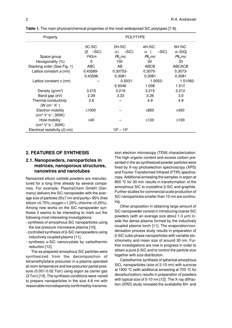
in Table 1 [7-9] and positions in the carbon and
silicon atoms arrangement and structures are dem-
onstrated in Fig. 1. The SiC polytype content is
defined by conditions of preparation (temperature,
pressure and environment) and presence of impu-
rities. It is considered that cubic polytype 3C-SiC is
more stable in comparison with other hexagonal
polytypes up to temperature of ~2100 °C [8].
8/8/2019 andrievski
http://slidepdf.com/reader/full/andrievski 2/20
2 R.A. Andrievski
Property POLYTYPE
3C-SiC 2H-SiC 4H-SiC 6H-SiC
(β –SiC) (α –SiC) (α –SiC) (α –SiC)
Space group F 43m P 63mc P 63mc P 63mc Hexagonality (%) 0 100 50 33
Stacking order (See Fig. 1) ABC AB ABCB ABCACB
Lattice constant a (nm) 0.43589- 0.30753- 0.3070- 0.3073-
0.43596 0.3081 0.3081 0.3081
Lattice constant c (nm) – 0.5031- 1.0053- 1.51092-
0.5048 1.008 1.512
Density (g/cm3) 3.215 3.219 3.215 3.212
Band gap (eV) 2.39 3.33 3.26 3.0
Thermal conductivity 3.6 – 4.9 4.9
(W cm-1 K-1)
Electron mobility ≤1000 – ≤850 ≤450(cm2 V-1s-1, 300K)
Hole mobility ≤40 – ≤120 ≤100
(cm2 V-1s-1, 300K)
Electrical resistivity (Ω cm) 102 – 103
Table 1. The main physical/chemical properties of the most widespread SiC polytypes [7-9].
2. FEATURES OF SYNTHESIS
2.1. Nanopowders, nanoparticles in
matrices, nanoporous structures,nanowires and nanotubes
Nanosized silicon carbide powders are manufac-
tured for a long time already by several compa-
nies. For example, PlasmaChem GmbH (Ger-
many) delivers the SiC nanopowder with the aver-
age size of particles 20±7 nm and purity> 95% (free
silicon <0.75%; oxygen <1.25%; chlorine <0.25%).
Among new works on the SiC nanopowder syn-
thesis it seems to be interesting to mark out the
following most interesting investigations:
- synthesis of amorphous SiC nanoparticles usingthe low pressure microwave plasma [10],
- controlled synthesis of β-SiC nanopowders using
inductively coupled plasma [11],
- synthesis α-SiC nanocrystals by carbothermic
reduction [12].
The as-prepared amorphous SiC particles were
synthesized from the decomposition of
tetramethylsilane precursor in a plasma operated
at room temperature and low precursor partial pres-
sure (0.001-0.02 Torr) using argon as carrier gas
(3 Torr) [10]. The synthesis conditions were varied
to prepare nanoparticles in the size 4-6 nm with
reasonable monodispersity confirmed by transmis-
sion electron microscopy (TEM) characterization.
The high organic content and excess carbon pre-
sented in the as-synthesized powder particles were
fixed by X-ray photoelectron spectroscopy (XPS)and Fourier-Transformed Infrared (FTIR) spectros-
copy. Additional annealing the samples in argon at
800 °C for 30 min results in transformation of the
amorphous SiC to crystalline β-SiC and graphite.
Further studies for commercial scale production of
SiC nanoparticles smaller than 10 nm are continu-
ing.
Other proposition in obtaining large amount of
SiC nanopowder consist in introducing coarse SiC
powders (with an average size about 1-3 µm) in-
side the dense plasma formed by the inductivelycoupled plasma torch [11]. The evaporation/con-
densation process study results in preparation of
β-SiC cubic phase nanoparticles with variable sto-
ichiometry and mean size of around 30 nm. Fur-
ther investigations are now in progress in order to
obtain a pure β-SiC and to control the particle size
together with size distribution.
Carbothermic synthesis of spherical amorphous
SiO2
nanoparticles (size of 2-10 nm) with sucrose
at 1500 °C (with additional annealing at 700 °C for
decarburization) results in preparation of powders
with typical size of 5-10 nm [12]. The X-ray diffrac-tion (XRD) study revealed the availability 6H- and
8/8/2019 andrievski
http://slidepdf.com/reader/full/andrievski 3/20
3Synthesis, structure and properties of nanosized silicon carbide
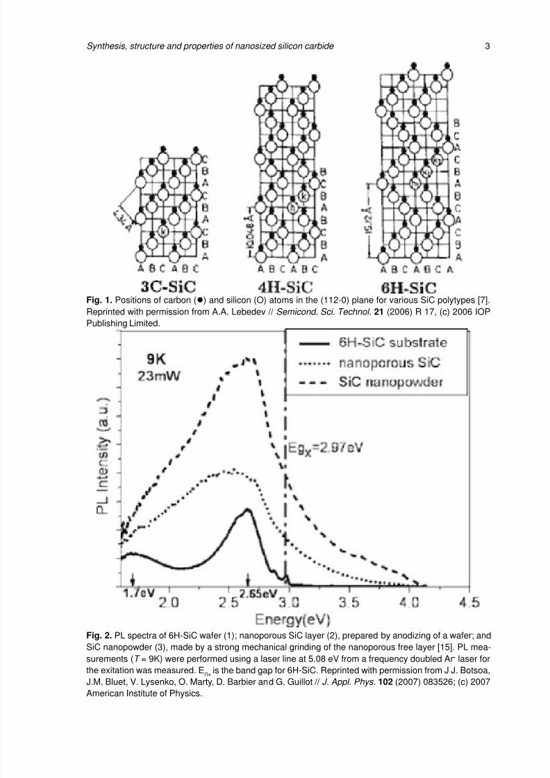
Fig. 1. Positions of carbon (l) and silicon (O) atoms in the (112-0) plane for various SiC polytypes [7].
Reprinted with permission from A.A. Lebedev // Semicond. Sci. Technol. 21 (2006) R 17, (c) 2006 IOP
Publishing Limited.
Fig. 2. PL spectra of 6H-SiC wafer (1); nanoporous SiC layer (2), prepared by anodizing of a wafer; and
SiC nanopowder (3), made by a strong mechanical grinding of the nanoporous free layer [15]. PL mea-
surements (T = 9K) were performed using a laser line at 5.08 eV from a frequency doubled Ar+
laser forthe exitation was measured. E
Gxis the band gap for 6H-SiC. Reprinted with permission from J J. Botsoa,
J.M. Bluet, V. Lysenko, O. Marty, D. Barbier and G. Guillot // J. Appl. Phys. 102 (2007) 083526; (c) 2007
American Institute of Physics.
8/8/2019 andrievski
http://slidepdf.com/reader/full/andrievski 4/20
4 R.A. Andrievski
4H-SiC polytypes with high density of stacking faults
and small amount of 2H and 3C phases. The size
effects have been observed in photoluminescence
(PL) spectra.
However, these results and other similar those
are only continuations and/or some specifications
of investigations (carbothermal synthesis, plasma
chemistry, laser synthesis, etc.) realized earlier and
reflected in reviews [4,5]. Now the primary atten-
tion of researchers is focused on preparation of
nanosized SiC inclusions in matrixes and of
nanowires/nanotubes as perspective materials for
opto - and nanoelectronics (light emitting diodes,
sensors, etc.) as soon as also porous ceramics for
high-temperature filters and catalytic supports. The
following basic technological methods are consid-
ered: electrochemical and chemical etching, car-
burization of silicon and silica, implantation of car-bon ions in silicon and joint implantation of ions of
carbon and silicon in SiO2
matrixes. These meth-
ods as applied to nanosized silicon (as a material
for nanoelectronics) were presented in book [13].
The nanosized SiC synthesis methods as applied
to electrical/optical properties were discussed by
results up to 2005 in review [14] with a compre-
hensive description of technological regimes.
By analogy with nanosized silicon [13], the PL
SiC spectra increase in nanoporous conditions is
also observed. Fig. 2 shows low temperature PL
spectra for 6H-SiC substrate, nanoporous SiC layer
and SiC nanoparticles by the size less than 10 nm
[15].
From these data the considerable PL increase
for two last subjects and especially for isolated
nanoparticles is clearly evident. This phenomenon
is connected with the quantum confinement effect.
It is considered also that the appreciable contribu-
tion in the PL increase is brought by defect struc-
ture on the nanopore surface that is formed at etch-
ing [14].
Electrochemical anode etching is carried out ata current density of 210 mA/cm2 in solution
HF:C2H
5OH (1:1) during 25 min [15]. For the de-
tachment of a porous layer (a thickness near by
100µm) from a substrate the current density quickly
increases to 1 A/cm2. It is also reported about the
possibility of refinement of usual 3C-SiC powder
(the particle size of some micrometers) to
nanoparticles by the size a little nanometer by
chemical etching in mix HNO3:HF (1:3) at 100 °C
within an hour with the subsequent centrifugation,
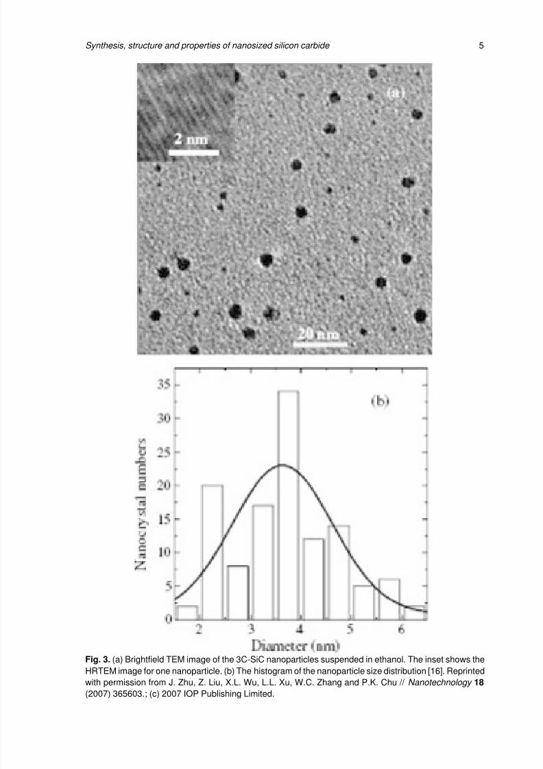
washing and so on [16].Fig. 3 displays the TEM image of SiC (including
high resolution TEM (HRTEM) image of one
nanocrystal) and the histogram of their distribution
in the sizes [16]. Apparently, synthesized
nanoparticles are nearly spherical with a diameter
ranging from 1.5 to 6.5 nm (the average size of
3.75 nm.), and the picture of the high resolution
testifies about high crystalinity with the lattice fringes
corresponding to the 111 plane of cubic polytype
3C-SiC. A little agglomeration of the nanoparticles
has been also pointed.
At preparation of porous SiC samples the pro-
cesses of carbide synthesis and formations of a
porous skeleton are usually combined, that allows
to considerably lower temperature of realization and
to organize nanoporous structure. So, heating of
the silicon powder mixes with fullerens or with soot
in Na steams (promoting mass transfer) at tem-
perature ~700 °C allows to synthesize β-SiC with
porosity about 70%. The pore size distribution wasin the range of 2-10 nm and grain size was in the
nanometer interval also [17]. Nanoporous silicon
carbide materials can be also prepared by the
polycarbosilane pyrolysis with and without the ad-
dition of an inert filler (nano- and microsized SiC
powders) [18]. Porous materials-based SiC
nanowires (diameter of ~100 nm) with honeycomb
structure are reported to prepare by carbothermal
reduction of silica [19].
The carbidization study of porous silicon, pre-
pared by electrochemical etching, has revealed the
3C-SiC nanocrystals formation with the size of 5-7
nm at temperature 1200-1300 °C [20]. It is sup-
posed also that due to the mechanism features, a
heterostructure is formed including Si nanocrystals
and nanosized amorphous SiC particles.
In a number of works (see, for example, [14,21-
23]) the features of the SiC nanoparticle implanta-
tion (ion beam) synthesis are investigated. In one
of the first studies [21] it has been established that
implantation of carbon ions with an energy of 50
keV and a dose of 1017 sm-2 in a silicon substrate
with the subsequent thermal annealing and elec-trochemical etching is accompanied by the occur-
rence of β-SiC nanocrystals and origin of a new
PL peak at about 445 nm (2.79 eV; see also Fig.
2). This new PL peak is 2.7 times as stronger than
that of the annealed and etched wafer without im-
plantation. The effect of the ion implantation doses
and temperature/duration annealing on structure
and optical properties of SiC synthesized
nanoparticles is investigated including a separate
implantation by carbon or silicon ions, and consecu-
tive double implantation by these ions with use asa substrate of SiO
2films [14,23]. In last case ac-
cording to electron paramagnetic resonance (EPR),
8/8/2019 andrievski
http://slidepdf.com/reader/full/andrievski 5/20
5Synthesis, structure and properties of nanosized silicon carbide
Fig. 3. (a) Brightfield TEM image of the 3C-SiC nanoparticles suspended in ethanol. The inset shows the
HRTEM image for one nanoparticle. (b) The histogram of the nanoparticle size distribution [16]. Reprinted
with permission from J. Zhu, Z. Liu, X.L. Wu, L.L. Xu, W.C. Zhang and P.K. Chu // Nanotechnology 18
(2007) 365603.; (c) 2007 IOP Publishing Limited.

8/8/2019 andrievski
http://slidepdf.com/reader/full/andrievski 6/20
6 R.A. Andrievski
Characteristic Authors
J. Chen et al. [25] J. Wei et al [26] F.-L. Wang [27]
Processing duration (h) 4-9 2 1
Diameter (nm) ~200 50-200 60-100Length (mm) 10-20 Several tenth mm Several mm
Section shape Hexagonal Hexagonal Roundish
Phase content β-SiC β-SiC β-SiC
a = 0.4353 Traces of a -SiC, a = 0.4370 nm
C and O SiO2-shell
SiO2-shell
PL presence n/d Peaks at 289 nm n/d
and 391 nm
Table 2. Characteristics of SiC nanowires [25-27].
XRD, XPS, PL spectra, HRTEM, scanning elec-
tron microscopy (SEM) and other methods, the
nanoinclusion formation after implantation and
additional annealing is noted. The identification of
formed phases and understanding of the got re-
sults with revealing of the mechanism of the SiC
nanocrystal/amorphous inclusion formation are not
so easy and need further investigation.
Implantation of silicon ions (a dose in the range
of 1016-2 1017 sm-2, energy 40 keV) in carbon
nanotubes was investigated in work [24]. Detailedstudying of structure and content of the implanted
tubes by HRTEM, XRD and energy-dispersive
spectroscopy (EDS) has fixed formation of amor-
phous SiC for which crystallization it is required
additional annealing.
Some studiess of the SiC nanowires synthesis
on the basis of direct interaction of silicon (or its
monoxide) with carbon (see, for example, [25-28])
are known. Reactions set on which synthesis SiC
is carried out can be written down by the following
way for different variants of interaction [25,27,28]:
2C O 2CO,S 2+ = (1 )
2Si O 2SiO ,G 2 G+ = (2)
SiO 2C SiC CO,G S S+ = + (3)
SiO CO SiC O ,G S 2+ = + (4)
3SiO 3C 2SiC SiO CO ,G S S 2 S 2+ = + +( ) (5)
SiO 3CO SiC 2CO ,G S 2+ = + (6)
CO C 2CO,2 S+ = (7)
3SiO CO SiC 2SiO ,G S 2 S+ = + ( ) (8)
4CO 6Si 4SiC 2SiO .S S 2 S
+ = + ( ) (9)
Some of these reactions promote the CO, SiO
and SiO2
reproducibility. The realization of that or
other reactions scheme depends on temperature
and level of supersaturation but practically they
have not studied in detail.
It is noticed that the SiC nanowires preparation
is possible by evaporation at 1600 °C in argon at-
mosphere using different initial products: silicon in
graphite crucible and a graphite substrate (reac-
tions (1-4)) [25], a mix of powders of silicon and
graphite activated by grinding [26] and mix of pow-
ders of silicon monoxide and soot activated by
plasma processing (reactions (5-8)) [27]. Table 2
presents comparison of these studies results car-
ried out practically simultaneously at three Chinese
universities and focused on large-scale synthesis.All technological processes are spent without
participation of catalysts, i.e. the most probable
mechanism of crystal growth can be represented
by the scheme of vapor - solid (without participa-
tion of a liquid phase). The growth direction of crys-
tals is along [111] direction. Fig. 4 shows a general
view of SiC nanowires having hexagonal (a and b)
and roundish (c) profile. In case of Figs. 4b and 4c,
the SiO2
shell presence is observed (on structural
data, the SiO2
shell is in an amorphous state).
From Table 2 and Fig. 4 it is quite obvious that
initial products make considerable impact on the
synthesis process but it is difficult to make a pref-
8/8/2019 andrievski
http://slidepdf.com/reader/full/andrievski 7/20
7Synthesis, structure and properties of nanosized silicon carbide
Deposition methods. Annealing Phase content Grain size, Test method
Authors. temperature (°C) (nm)
Reactive magnetron sputtering 1100 β-SiC 7.3±0.4 XRD
with using Si/C targets 3-10 HRTEM
(Si substrate) [32]
The same (ion energy of 950 80% β-SiC 8-10 XRD
~90 eV; temperature deposition 1140 85%(α+β)-SiC 17 XPS
700-1050 °C; Si, Al2O
3, Mo,
SiO2
substrates) [33]
Reactive magnetron sputtering – β-SiC 4-5 HRTEM
in a plasma of (H2+Ar) at
200-600 °C (Si substrate) [35]
Plasma Enhanced CVD in 1300 2H-SiC+4H-SiC 15 HRTEM
(CH4 /SiH
4 /Ar) gases on Si/SiO
25 XRD
substrates at 350 °C [36]Hot-Mo wire CVD using – 3C-SiC 6-12 XRD
(SiH
4 /CH
4 /H
2) gases at
104-434 °C [37]
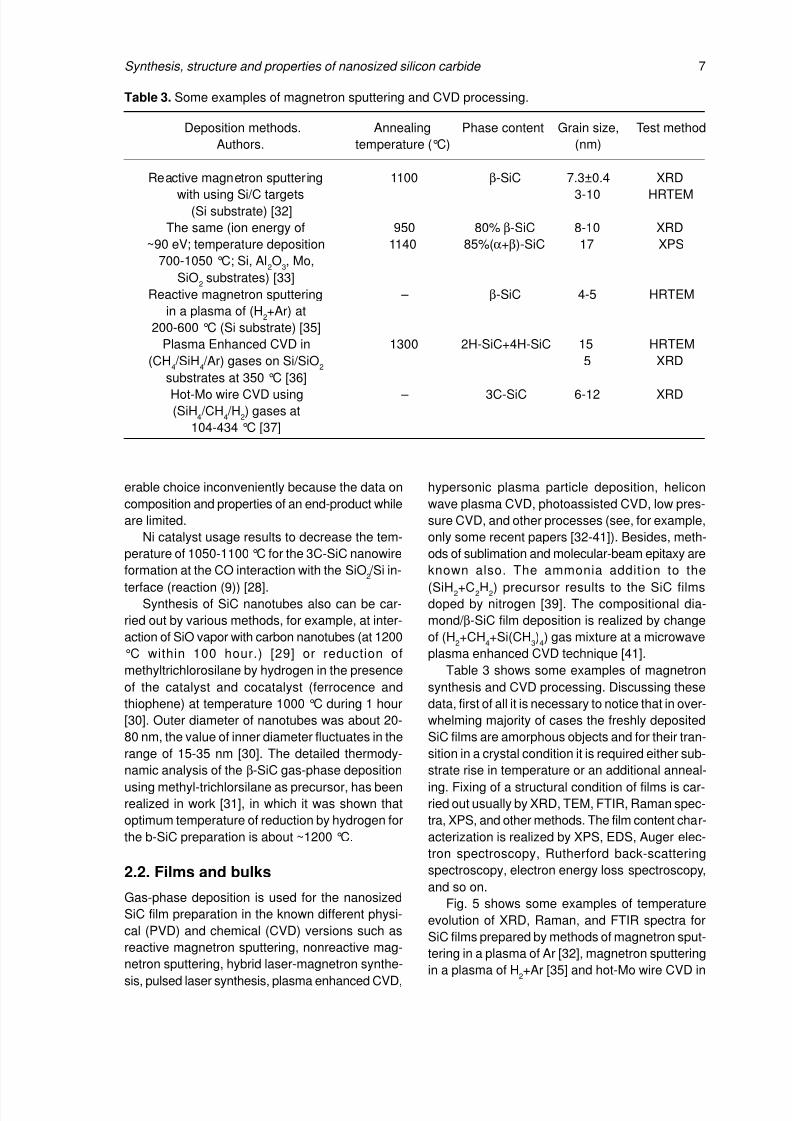
Table 3. Some examples of magnetron sputtering and CVD processing.
erable choice inconveniently because the data on
composition and properties of an end-product while
are limited.
Ni catalyst usage results to decrease the tem-
perature of 1050-1100 °C for the 3C-SiC nanowire
formation at the CO interaction with the SiO2 /Si in-terface (reaction (9)) [28].
Synthesis of SiC nanotubes also can be car-
ried out by various methods, for example, at inter-
action of SiO vapor with carbon nanotubes (at 1200
°C within 100 hour.) [29] or reduction of
methyltrichlorosilane by hydrogen in the presence
of the catalyst and cocatalyst (ferrocence and
thiophene) at temperature 1000 °C during 1 hour
[30]. Outer diameter of nanotubes was about 20-
80 nm, the value of inner diameter fluctuates in the
range of 15-35 nm [30]. The detailed thermody-
namic analysis of the β-SiC gas-phase deposition
using methyl-trichlorsilane as precursor, has been
realized in work [31], in which it was shown that
optimum temperature of reduction by hydrogen for
the b-SiC preparation is about ~1200 °C.
2.2. Films and bulks
Gas-phase deposition is used for the nanosized
SiC film preparation in the known different physi-
cal (PVD) and chemical (CVD) versions such as
reactive magnetron sputtering, nonreactive mag-netron sputtering, hybrid laser-magnetron synthe-
sis, pulsed laser synthesis, plasma enhanced CVD,
hypersonic plasma particle deposition, helicon
wave plasma CVD, photoassisted CVD, low pres-
sure CVD, and other processes (see, for example,
only some recent papers [32-41]). Besides, meth-
ods of sublimation and molecular-beam epitaxy are
known also. The ammonia addition to the(SiH
2+C
2H
2) precursor results to the SiC films
doped by nitrogen [39]. The compositional dia-
mond/ β-SiC film deposition is realized by change
of (H2+CH
4+Si(CH
3)
4) gas mixture at a microwave
plasma enhanced CVD technique [41].
Table 3 shows some examples of magnetron
synthesis and CVD processing. Discussing these
data, first of all it is necessary to notice that in over-
whelming majority of cases the freshly deposited
SiC films are amorphous objects and for their tran-
sition in a crystal condition it is required either sub-
strate rise in temperature or an additional anneal-
ing. Fixing of a structural condition of films is car-
ried out usually by XRD, TEM, FTIR, Raman spec-
tra, XPS, and other methods. The film content char-
acterization is realized by XPS, EDS, Auger elec-
tron spectroscopy, Rutherford back-scattering
spectroscopy, electron energy loss spectroscopy,
and so on.
Fig. 5 shows some examples of temperature
evolution of XRD, Raman, and FTIR spectra for
SiC films prepared by methods of magnetron sput-
tering in a plasma of Ar [32], magnetron sputteringin a plasma of H
2+Ar [35] and hot-Mo wire CVD in

8/8/2019 andrievski
http://slidepdf.com/reader/full/andrievski 8/20
8 R.A. Andrievski
a
b
c
Fig. 4. Typical SEM images of SiC nanowires.
the presence of SiH4, CH
4, and H
2gases [37]. Tem-
perature conditions of crystallization of those or
other SiC polytypes all are various and depend on
experimental conditions and many kinetic param-
eters. There are the different characteristics of vari-
ous temperature dependences of crystallite growth
(for example, non-monotone change with a maxi-
mum at 280 °C for tests [37], monotonous that with
temperature growth [33] and unthermal that in an
interval of 200-600 °C in experiments [35]). All it
testifies to necessity of the further continuation of
studies.
Recently the method of the solid-state epitaxy
of SiC film on silicon consisting in processing of Si
single-crystal by CO (T = 1100-1400 °C, P CO
=
10-300 Pa, t =5-60 min.) has been developed [42].
It is considered that this interaction results in the
silicon vacancy formation in surface layers and
the stress relaxation promotion (the stresses
arise because of a discrepancy between SiC/Si
lattices). It provides the solid-state epitaxy of SiC
films growing on silicon with thickness of 20-100
nm. Fig. 6 shows the Pl spectra of 4H and 3C
polytypes.
8/8/2019 andrievski
http://slidepdf.com/reader/full/andrievski 9/20
9Synthesis, structure and properties of nanosized silicon carbide
a
b
c
Fig. 5. Temperature effect in Raman (a ) replotted
from [32], XRD (b ) [35], and FTIR (c ) replotted from
[37] spectra of SiC films. In Fig. 5, a : a-Si and a-C
are amorphous silicon and carbon; TO and LO are
transverse and longitude optical modes; D-band
and G-band are vibration modes in carbon
sublattice. Fig. 5b - reprinted with permission from
H. Colder, R. Rizk, M. Morales, P. Marie and J.
Vicens // J. Appl. Phys. 98 (2005) 024313; (c) 2006
American Institute of Physics.
Liquid-phase epitaxy of 2H-SiC film on a (0001)
4H-SiC substrate in Li-Si melt at 850 °C (t =48 hour.)
is described in work [43].In comparison with the SiC nanosized film
preparation, attempts of manufacturing bulk
nanomaterials are less successful [4,5]. Intensive
recrystallization of nanopowders at consolidation
temperatures complicates the preparation of bulk
nanostructured materials. As applied to
nanopowders only using methods of high pressures
and high temperatures (sintering at T ~1200 °C and
under pressure of 2-8 GPa) results in making
SiC samples with nanograin size [44]. Examples
of the dense sample preparation by sintering
SiC nanopowders, activated by mechanosynthesis,and high-porous materials by reactive sintering
C/Si nanopowders have been described
early [4].
3. STRUCTURE AND PROPERTIES
3.1. Structural features and content
Table 4 demonstrates the difference in the stoichio-
metric coefficients and carbon vacancy concentra-
tion for different SiC polytypes [45].
The structure studies of nano-SiC polytypes are
not so detailed yet to judge the effect of size factor
on a deviation from stoichiometry and vacancy
characterization. There are the following values of
the cubic SiC-polytype lattice parameter a (in nm)
such as 0.436 (the grain size of 4-7 nm) [17]; 0.4353
(the nanowire diameter of 200 nm) [25]; 0.4370 (the
RAMAN SHIFT, cm-1
400 800 1200 1600 2000
I N T E N S I T Y
, a r b
i t r a r y u n
i t s
AS-DEPOSITED
a-C800 °C
1000 °C
1100 °C
a-SiTO LO
D-band G-band
C-CSi-CSi-Si
600 800 1000 12000,0
0,5
1,0
1,5
2,0
A b s o r p
t i o n c o e
f f i c
i e n
t a
( [ 1 0
4 c
m - 1 )
Wawenumber (cm-1)
2000C
3000C
4000C
5000C
6000C 2000 2500 3000
0,2
0,4
8/8/2019 andrievski
http://slidepdf.com/reader/full/andrievski 10/20
10 R.A. Andrievski
Fig. 6. PL spectra of 4H-SiC and 3C-SiC polytypes (T = 77K) [42]. Reprinted with permission from S.A.
Kukushkin and A.V. Osipov // Phys. Sol. State 50 (2008) 1238 (English transl.); (c) 2008 MAIK Nauka/
Interperiodika
nanowire diameter of 60-100 nm) [27]; 0.4361 (the
nanowire diameter of 60-70 nm) [28]; 0.438 (the
grain size of 2-5 nm) [35]. The a and c values for
6H-polytype are 0.309 nm and 1.525 nm accord-
ingly [35]. These values in the majority are compa-rable with those given in Table 1; however, it is hard
to judge the influence of size effect or impurity con-
tent on lattice parameter. Nevertheless, the lattice
parameter increase in nanoinclusions of α - and Β
- polytypes, in comparison with their volume coun-
terparts is marked [35].
Allocation of carbon, argon and hydrogen at theannealing of amorphous and nanocrystalline SiC
films was investigated in a number of works (see,

8/8/2019 andrievski
http://slidepdf.com/reader/full/andrievski 11/20
11Synthesis, structure and properties of nanosized silicon carbide
Characteristic 3C 6H 15R 4H
Si/C 1.046 1.022 1.012 1.001
N C
(1020 cm-3) 33.6 16.3 15.1 7.3
Table 4. Stoichiometry and mean concentration of
vacancies in different SiC polytypes [45].
Fig. 7. Cross-sectional TEM micrographs for films deposited at T =200 °C (a ), T =300 °C (b ), T =400 °C (c ),
and at T =600 °C (d ) [35]. In the inset, the corresponding SAED patterns. Reprinted with permission from
H. Colder, R. Rizk, M. Morales, P. Marie and J. Vicens // J. Appl. Phys. 98 (2005) 024313; (c) 2005
American Institute of Physics.
for example, [33,34,36,46,47]). The XRD, HRTEM,
FTIR, Raman spectra, XPS methods have allowed
to track temperature changes in the Si - Si, C - Cand Si – C covalent bonds and reveal the change
of content and structure of films. EDS method has
revealed the following temperature change of car-
bon and silicon at the film deposition by electron
beam evaporation: 24.18 at .%C and 75.5.65 at.%Si
(T =500 °C); 17.95% C and 81.12% Si (T =1000 °C);
15.20% C and 83.51% Si (T =1200 °C) [34]. The
silicon excess in these data is connected with the
substrate effect; the presence of impurity of oxy-
gen is noted also.
Fig. 7 shows the cross-section sections of
HRTEM images of films SiC deposited by magne-
tron sputtering in Ar/H2
plasma at different tem-
peratures of silicon substrate [35].
As can be seen from these data (includingmicrodiffraction information on inserts), with in-
crease temperature of the SiC nanoinclusion (6H
8/8/2019 andrievski
http://slidepdf.com/reader/full/andrievski 12/20
12 R.A. Andrievski
Fig. 8. AFM – image of SiC nucleuses formed by deposition of carbon on Si substrate (the stream of 5
1013 cm-2 s-1; T =925 °C; t =10 s). Reprinted with permission from Yu. V. Trushin, E. E. Zhurkin, K. L.
Safonov, A. A. Schmidt, V. S. Kharlamov, S. A. Korolev, M. N. Lubov and J. Pezoldt // Techn. Phys. Lett.
30 (2004) 641; (c) 2004 MAIK "Nauka/Interperiodika".
or 3C polytypes) crystallization makes progress in
an amorphous matrix that is also shown in evolu-tion of IR spectra (see earlier Fig. 5). The analysis
of the received information has found out the pres-
ence of stacking faults and twins. The analogous
situation in the SiC layer deficiencies and presence
of stacking faults and twins have been observed in
films produced by CVD technology with use of
(C3H
8+SiH
4) precursor [48]. The origin of these pla-
nar defects is connected both with features of crys-
tal growth on border of system SiC/Si and with low
energy of stacking defects in silicon carbide. The
size dependence of twin formation energy in
nanosized cubic SiC is analyzed in paper [49].
The porosity and various polytype formation
(with their following junction and stacking fault
nucleation) was fixed in the case of SiC films pre-
pared by solid-phase epitaxy method [50].
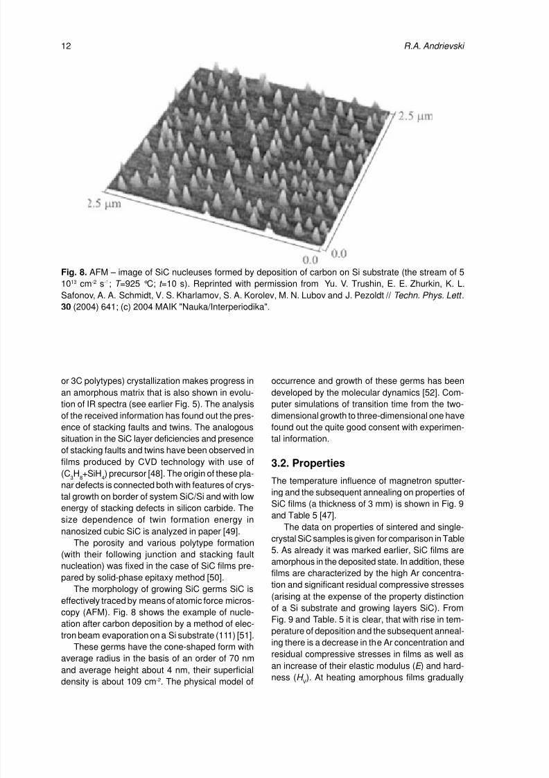
The morphology of growing SiC germs SiC is
effectively traced by means of atomic force micros-
copy (AFM). Fig. 8 shows the example of nucle-
ation after carbon deposition by a method of elec-
tron beam evaporation on a Si substrate (111) [51].
These germs have the cone-shaped form with
average radius in the basis of an order of 70 nmand average height about 4 nm, their superficial
density is about 109 cm-2. The physical model of
occurrence and growth of these germs has been
developed by the molecular dynamics [52]. Com-puter simulations of transition time from the two-
dimensional growth to three-dimensional one have
found out the quite good consent with experimen-
tal information.
3.2. Properties
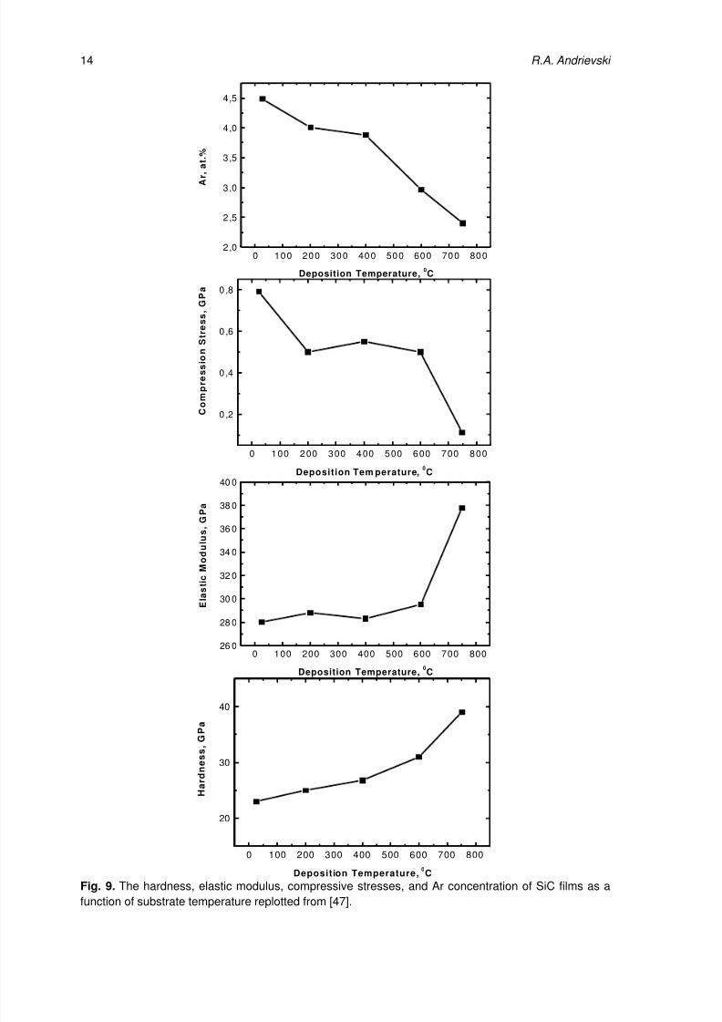
The temperature influence of magnetron sputter-
ing and the subsequent annealing on properties of
SiC films (a thickness of 3 mm) is shown in Fig. 9
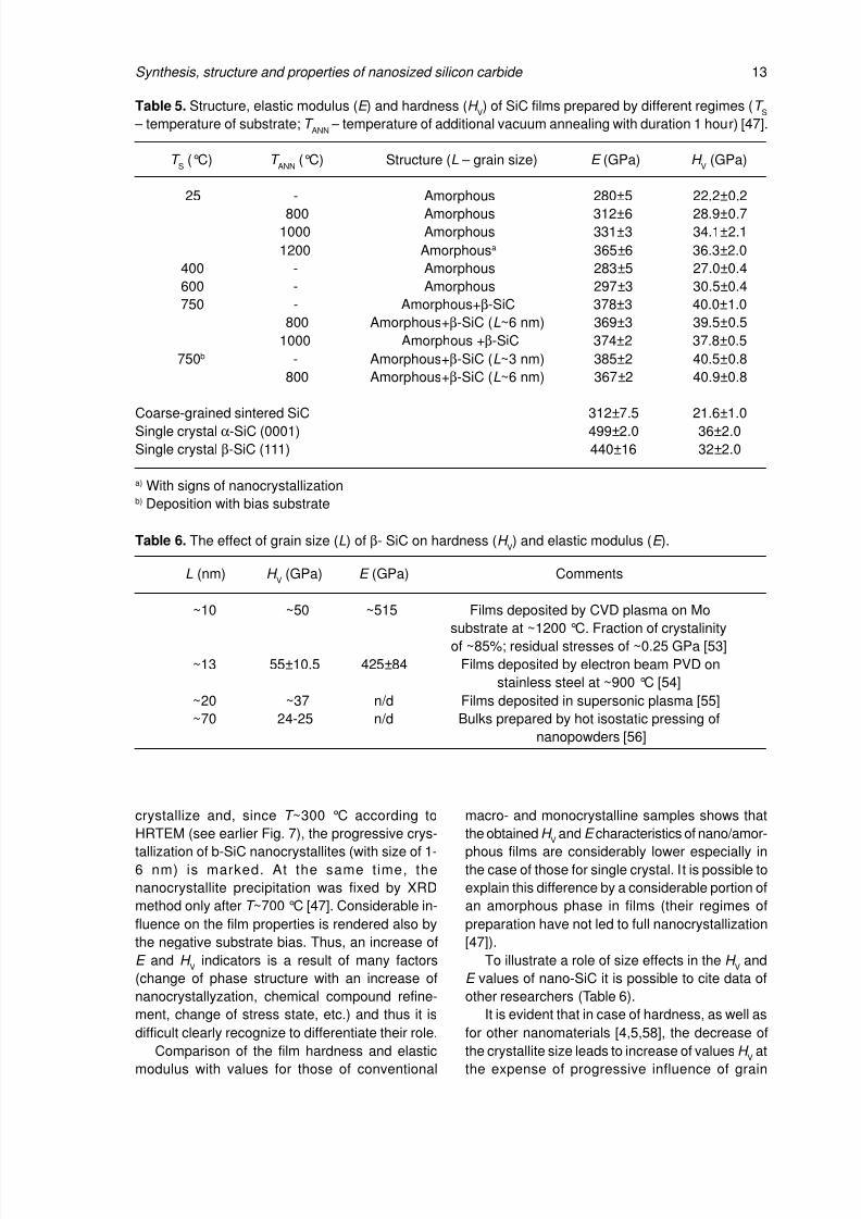
and Table 5 [47].
The data on properties of sintered and single-crystal SiC samples is given for comparison in Table
5. As already it was marked earlier, SiC films are
amorphous in the deposited state. In addition, these
films are characterized by the high Ar concentra-
tion and significant residual compressive stresses
(arising at the expense of the property distinction
of a Si substrate and growing layers SiC). From
Fig. 9 and Table. 5 it is clear, that with rise in tem-
perature of deposition and the subsequent anneal-
ing there is a decrease in the Ar concentration and
residual compressive stresses in films as well as
an increase of their elastic modulus (E ) and hard-
ness (H V). At heating amorphous films gradually
8/8/2019 andrievski
http://slidepdf.com/reader/full/andrievski 13/20
13Synthesis, structure and properties of nanosized silicon carbide
T S
(°C) T ANN
(°C) Structure (L – grain size) E (GPa) H V
(GPa)
25 - Amorphous 280±5 22.2±0.2
800 Amorphous 312±6 28.9±0.7
1000 Amorphous 331±3 34.1±2.1
1200 Amorphousa 365±6 36.3±2.0
400 - Amorphous 283±5 27.0±0.4
600 - Amorphous 297±3 30.5±0.4
750 - Amorphous+β-SiC 378±3 40.0±1.0
800 Amorphous+β-SiC (L~6 nm) 369±3 39.5±0.5
1000 Amorphous +β-SiC 374±2 37.8±0.5
750b - Amorphous+β-SiC (L~3 nm) 385±2 40.5±0.8
800 Amorphous+β-SiC (L~6 nm) 367±2 40.9±0.8
Coarse-grained sintered SiC 312±7.5 21.6±1.0Single crystal α-SiC (0001)
499±2.0 36±2.0
Single crystal β-SiC (111) 440±16 32±2.0
a) With signs of nanocrystallizationb) Deposition with bias substrate
Table 5. Structure, elastic modulus (E ) and hardness (H V) of SiC films prepared by different regimes (T
S
– temperature of substrate; T ANN
– temperature of additional vacuum annealing with duration 1 hour) [47].
L (nm) H V
(GPa) E (GPa) Comments
~10 ~50 ~515 Films deposited by CVD plasma on Mo
substrate at ~1200 °C. Fraction of crystalinity
of ~85%; residual stresses of ~0.25 GPa [53]
~13 55±10.5 425±84 Films deposited by electron beam PVD on
stainless steel at ~900 °C [54]
~20 ~37 n/d Films deposited in supersonic plasma [55]
~70 24-25 n/d Bulks prepared by hot isostatic pressing of
nanopowders [56]
Table 6. The effect of grain size (L) of β- SiC on hardness (H V) and elastic modulus (E ).
crystallize and, since T ~300 °C according to
HRTEM (see earlier Fig. 7), the progressive crys-
tallization of b-SiC nanocrystallites (with size of 1-
6 nm) is marked. At the same time, the
nanocrystallite precipitation was fixed by XRD
method only after T ~700 °C [47]. Considerable in-
fluence on the film properties is rendered also by
the negative substrate bias. Thus, an increase of
E and H V
indicators is a result of many factors
(change of phase structure with an increase of
nanocrystallyzation, chemical compound refine-
ment, change of stress state, etc.) and thus it is
difficult clearly recognize to differentiate their role.Comparison of the film hardness and elastic
modulus with values for those of conventional
macro- and monocrystalline samples shows that
the obtained H V
and E characteristics of nano/amor-
phous films are considerably lower especially in
the case of those for single crystal. It is possible to
explain this difference by a considerable portion of
an amorphous phase in films (their regimes of
preparation have not led to full nanocrystallization
[47]).
To illustrate a role of size effects in the H V
and
E values of nano-SiC it is possible to cite data of
other researchers (Table 6).
It is evident that in case of hardness, as well as
for other nanomaterials [4,5,58], the decrease ofthe crystallite size leads to increase of values H
Vat
the expense of progressive influence of grain
8/8/2019 andrievski
http://slidepdf.com/reader/full/andrievski 14/20
14 R.A. Andrievski
Fig. 9. The hardness, elastic modulus, compressive stresses, and Ar concentration of SiC films as a
function of substrate temperature replotted from [47].
0 100 200 300 400 500 600 700 8002,0
2,5
3,0
3,5
4,0
4,5
A r ,
a t . %
Deposition Temperature,0C
0 100 200 300 400 500 600 700 800
0,2
0,4
0,6
0,8
C o m p r e s s i o n S t r e s s ,
G P a
Deposition Tem perature,0C
0 100 200 300 400 500 600 700 80026 0
28 0
30 0
32 0
34 0
36 0
38 0
40 0
E l a s t i c M o d u l u s , G
P a
Deposition Temperature,0C
0 100 200 300 400 500 600 700 800
20
30
40
H a r
d n e s s ,
G P a
Deposition Temperature,0C

8/8/2019 andrievski
http://slidepdf.com/reader/full/andrievski 15/20
15Synthesis, structure and properties of nanosized silicon carbide
Fig. 10. Behavior at deformation (T= 1800 °C, strain rate of 10-1 s-1) of β- SiC specimens prepared by hot
pressing (grain size of 2 mm) and hot isostatic pressing (grain size of ~0.2 µm) replotted from [65].
boundaries as strong barriers to distribution of dis-
locations and cracks. For the elastic modulus this
dependence has other character: a decrease in
values E is observed at the crystallite size for dif-
ferent materials approximately at level less than
30-50 nm at the expense of the part increase of
grain boundaries which elastic characteristics are
lower in comparison with those for regular crystal
state [58]. In the general view, the nano-SiC prop-
erties should depend not only from the crystallite
size but also from the structure crystallinity, i.e. partin it an amorphous component, and also the spe-
cific properties and structure of these components.
It is accepted to analyze also properties nano/amor-
phous SiC composites comparing them with the
relation sp 3 / sp 2 the carbon configurations taken
from Raman spectrometry and XPS and meaning
that sp 3 – the configuration corresponds to dia-
mond, and sp 2 – one is to amorphous carbon (see,
for example, [54,55]). In the light of told quite clearly
that the establishment of dependences H V
= f (L)
and E = f (L) for SiC nanomaterials with allocation
of a part of the different factor influence requires
the further studying. Nevertheless it is quite obvi-
ous that there is an essential hardness increase
with reduction of the size of grain for SiC as well as
for other high-melting point compounds [4,5]. It is
noticed also that preliminary results testify in the
some increase of fracture toughness (K IC
): for films
β-SiC with the grain size of 10-15 nm (the width of
grain boundaries of 1-2 nm): for usual coarse-
grained SiC materials the K IC
value is about 2-6
MPa1/2 and this indicator for nanostructured SiC
films is of 9.2±2 MPa1/2 [54,57].
The problem of the strength of brittlenanomaterials-based SiC and other high-melting
point compounds is investigated theoretically in
frameworks of physics and mechanics of a solid
state (see, for example, [58-61]). Such questions
as homogeneous and heterogeneous formation of
dislocations, origin and movement of cracks on
grain boundaries, grain boundary sliding and so on
were analyzed.
It is necessary to consider as the most interest-
ing experimental result the observation in situ of
plastic deformation at the β-SiC (Ø70-100 nm)
nanowire testing in HRSEM and HRTEM [62,63].
The testing temperature was close to room and
NOMINAL STRAIN, %
TRUE STRAIN
0 120
200
250
6020
0.10 0.4 0.5 0.6 0.70.2 0.3
0
T R U E S T R E S S ,
M P a
Hot pressed SIC, d =2µm
HIPed SiC, d =0.2µm

8/8/2019 andrievski
http://slidepdf.com/reader/full/andrievski 16/20
16 R.A. Andrievski
Fig. 11. The temperature effect on electrical resistance 3C SiC/6H SiC heterostructures: 1-4 –
heterostructures with different level of alloying layer 3C; 5 – substrate 6H. In the inset, the temperature
dependence for heterostructures in low-temperature interval. Reprinted with permission from A. A. Lebedev,
P. L. Abramov, N. V. Agrinskaya, V. I. Kozub, A. N. Kuznetsov, S. P. Lebedev, G. A. Oganesyan, L. M.
Sorokin, A. V. Chernyaev and D. V. Shamshur // Techn. Phys. Lett. 33 (2008) 1035; (c) 2008 MAIK
"Nauka/Interperiodika".
deformation made more than 200%. An increase
of dislocation density at an initial stage and struc-
ture amorphization at a final stage were fixed. It is
necessary to note the results of computer experi-
ment (the model with the sizes of 62.5×62.5×53.5
nm3 contained 18.7 million atoms; the grain size
was of 8 nm) in which the presence of grain bound-
ary slidings at the first stage of deformation and
the subsequent transgrain dislocation shears have
been revealed at a room temperature [64].
The deformation behavior (T =1800 °C) of β-SiC
samples with the grain size of ~2 mm and ~0.2
mm is shown in Fig. 10 [65]. It is evident that this is
a typical brittle deformation for coarsegrain samples
and the objects with structure close to
nanostructure find out superplasticity (deformation
of ~110 %).Pertinently to underline that as a rule the tem-
perature of brittle-plastic transition for usual coarse-
grained β-SiC samples is not lower 900°-1200 °C
[66] (by data of Fig. 10 even more 1800 °C) i.e. a
decrease of this characteristic can be considerable
enough in the case of transition to nanomaterials
but the realization of this advantage is very hard
for massive (bulk) nanosubjects as the technology
of their preparation should provide the high
nanostructure perfection with an exception of nano
- and microporosity and other defects both in
nanograins and especially on their grain bound-
aries.
Let us consider the characteristic of the nano-
SiC physical properties. Earlier in Fig. 2, by data
[15], evolution of PL spectra for 6H-SiC at transi-
tion from coarse-grained substrates to nanoporous
sample and isolated nanoparticle was already
shown. Many examples of similar changes of lu-minescence and optical properties of nano-SiC (on
an example of nanoparticles, nanowires,
T , K
8/8/2019 andrievski
http://slidepdf.com/reader/full/andrievski 17/20
17Synthesis, structure and properties of nanosized silicon carbide
nanotubes, nanofilms, and quantum points) with
the analysis of theoretical results are resulted in
review [14]. The theory of the PL spectra change
and widening of band gap in connection with quan-
tum-dimensional effect (quantum confinement ef-
fect) is based on the analysis of band structure tak-
ing into account finiteness of the nanocrystallite
size. As it is known that energy of electronic exci-
tation in nanosemiconductors surpasses energy of
band-to-band transition in corresponding macro-
scopic semiconductors. With reference to nano-Si
it is in detail described in monograph [13]. Proceed-
ing from theoretical estimations, the widening of
band gap for hexagonal polytype 6H-SiC begins at
radius of nanosubjects less than ~7 nm (an abrupt
ascension since the sizes of <3 nm); for cubic
polytype 3C-SiC these sizes make accordingly of
<4 nm and of <1.5 nm [14]. Most full theoreticaland experimental studies were carried out for cu-
bic polytype in which the value of the band gap for
diameters of 3.9 nanometers and 8.8 nanometers
have appeared ~2.7 eV and ~2.3 eV correspond-
ingly (last value is close to tabular that – see Table
1) [67].
The optical properties, chemisorption charac-
teristics and stability of SiC nanotubes (in various
forms depending on their geometrical sizes and
chirality) have been estimated theoretically from the
first principles – ab initio [68-71]. For example, it is
shown that NO2
molecules can be chemisorbed
on SiC nanotubes in contrast with either carbon
nanotubes or boron nitride those.
Study of electrical and galvanomagnetic prop-
erties of amorphous SiC:H films and epitaxial 3C-
SiC films has been undertaken in papers [72,73].
Effect of annealing of amorphous films on their
conductivity resulted in the reveal of the activation
energy temperature dependence [72]. The tem-
perature dependence of the 3C-SiC film specific
electrical resistance on a substrate 6HSiC is shown
in Fig. 11 [73].Apparently from these data, is shown that with
temperature fall the heterostructure 3C-SiC/6HSiC
electrical resistance (ρ) increases gradually on the
exponential law and at T <50K this change is pro-
portional to T 1/3. At temperature of liquid nitrogen
(77K) the ρ value of a substrate (hexagonal
polytype) is approximately on 2 order above than
the ρ value of films. The studied epitaxial layers
possessed conductivity of n-type; concentration of
carriers and their mobility at 300K made 2 1018
cm-3
and 40 cm2
/V sec and that is close enough totabular data (see Table 1). The analysis of results
has shown also that low resistance of these layers
at helium temperatures can be connected with tran-
sition from insulator to metal.
Data on electrical and optical properties of 3C-
SiC/6H-SiC heterostructures and superlattices
(multilayered films) on their basis with reference to
electronics problems are generalized in review [7].
Recently works on research of the irradiation
influence on properties of nano-SiC have begun.
The comparison of structural evolution of samples
3C-SiC in a usual crystal condition (the grain size
of ~1 µm, porosity of 15%) and with nanostructure
(the grain size of ~36 nm, porosity of 8%) has
shown that the irradiation at a room temperature
by ions Xe (energy 95 MeV; dose 5×10¹⁴ sm-2) is
accompanied approximately by identical changes
of the cell parameter and does not lead to the struc-
ture amorphization [74]. While the irradiation of the
monocrystalline 6H-SiC at room temperature withlow energy ions resulted in the total amorphization.
The change of PL, IR, XRD, and Raman spectra
after joint implantation of C and Ca ions in 6H-SiC
thin films is analysed in paper [75].
Encouraging results of the biological property
study of amorphous SiC films with reference to bio-
medical applications are marked in a number of
works (see review [76] and Refs. in it). Tests in
vivo and in vitro have revealed, for example, that
the SiC biocompatibility with cages of the animal
organisms possessing ability to grasp and digest
alien particles (phagocytosis). However, an accu-
mulation of regular data on the nano-SiC biologi-
cal characteristics only begins. It is especially im-
portant in connection with known risks concerning
toxicity of nanosubjects.
4. CONCLUSIONS
The investigation of the nano-SiC properties has
revealed many interesting results among which first
of all we will note the possibility of the hardness
essential increase, display of the nanowire highplasticity, substantial increase of the PL spectra
intensity, biocompatibility, good resistance to
amorphization under irradiation and some other.
Traditional scopes of the SiC material application
(such as abrasives, refractories, heaters, some
semiconductor devices, additives to composites,
nanosized powders, etc.) have received a good
impulse to potential expansion. The high biologi-
cal compatibility and wear resistance of nano-SiC
made these materials perspective as coverings for
the implanted microelectrodes and the worn out
joints as well as in high-porous membranes and
biosensors [76]. Chemical inertness and
8/8/2019 andrievski
http://slidepdf.com/reader/full/andrievski 18/20
18 R.A. Andrievski
biocompatibility in connection with optical proper-
ties open the possibilities of the SiC quantum points
using for fluorescing diagnostics in medicine [77].
The prospects of these materials in opto – and
nanoelectronics [7,78], in MEMS and NEMS sys-
tems it is quite obvious [79,80] as well as for po-
rous high-temperature filters and catalyst supports
[17,19]. High radiation resistance of SiC
nanomaterials makes them very perspective as an
important candidate for the nuclear fusion reactors
like ITER and high-temperature gas cooled reac-
tors [74,81]. It is also important to take attention to
the novel hard amorphous nanocomposite Si-B-
C-N coatings with oxidation resistance above 1000
°C [82].
The realization of listed applications substan-
tially depends on efficiency of the nano-SiC manu-
facturing technology method. Here pertinently tonote a method working out the solid-state epitaxy
of SiC film on silicon [42]. It is considered that the
layers received thus nano-SiC will find applications
as substrates, light-emitting diodes and solar bat-
teries [83]. On the other hand, the possibilities of
consolidated bulk nano-SiC materials [84] seems
to be more productive in near future. There are
some encourage results of spark plasma sintering
nanoscale SiC structures [85]. As a result, the ne-
cessity of comparison of the nano-SiC manufac-
turing technology various methods, as it was
marked early, is very urgent.
At the same time the lack of data about the sta-
bility of physical, chemical, and mechanical prop-
erties of these materials and accordingly of their
operational characteristics is felt. Certainly, the
nano-SiC wide realization demands also the fur-
ther development of basic researches in the field
of dimensional effects.
ACKNOWLEDGEMENTS
The support of the Russian Found of Basic Re-search (Projects No 08-03-00105 and No 09-03-
11000) and the Program of Fundamental Re-
searches of Russian Academy of Sciences (Sub-
programs P-18 and P-27) is acknowledged. The
author is grateful to Mr. V.V. Klucharev, Mrs. S.V.
Klucharev, and Dr. A.V. Khatchoyan for their active
help in the review preparation as well as to Prof.
D.I. Tetelbaum for fruitful discussion.
REFERENCES
[1] Silicon Carbide 2006 Materials Processing and Devices. Vol. 911, ed. by M. Dudley,
M. Capano, T. Kimono, A.R. Powell and Sh.Wang (Mater. Res.Soc., Warrendale, 2006).
[2] Silicon Carbide and Related Materials.
ECSCRM 2006. Vols. 556-557 , ed. byN. Wright, C.M. Johnson, K. Vassilevski,I. Nikitina and A. Horsfall (Trans. Tech. Publ.Mater. Sci. Forum, Switzerland, 2007).
[3] Silicon Carbide 2008 Materials, Processing
and Devices. Vol. 1069, ed. by M. Dudley,C.M. Johnsohn, A.R. Powell and S.-H. Ryu(Mater. Res. Soc., Warrendale, 2008).
[4] R.A. Andrievski // Russ. Chem . Rev. 74
(2005) 1061 (English transl.).[5] R.A. Andrievski, In: Nanomaterials handbook ,
ed. by Y. Gogotsi (CRC Press: Boca RatonFL, 2006), p. 405.
[6] R.A. Andrievski // Nanotechnologies in Russia
2 (2007) 6 (English transl.).[7] A.A. Lebedev // Semicond. Sci. Technol. 21
(2006) R 17.[8] L.L. Snead, T, Nozawa, Y, Katoh, T.-S. Byun,
S. Kondo and D.A. Petti // J. Nucl. Mater. 371
(2007) 329.[9] S.A. Kukushkin, A.V. Osipov, V.N. Bessolov,
B.K. Medvedev, V.K. Nevolin and K.A. Tcarik// Rev. Adv. Mater. Sci. 17 (2008) 1.
[10] H. Lin, J.A. Gerbec, M. Sushchikh and E.W.McFarland // Nanotechnology 19 (2008)325601-08.
[11] Y. Leconte, M. Leparoux, X. Portier andN. Herlin-Boime // Plasma Chem. Plasma
Process. 28 (2008) 233.[12] A.A. Zhokhov, V.M. Masalov, D.V. Matveev,
M.Y. Maksimuk, I.I. Zverkova,S.S.Khasanov, S.Z. Shmurak, A.P.Bazhenov and G.A. Emelchenko // Phys.
Sol. State 51 (2009) 1626 (English transl.).[13] N.N. Gerasimenko and Yu.N. Parkhomenko,
Silicon material for nanoelectronics
(Technosphera, Moscow, 2007), in Russian.
[14] J.Y. Fan, X.L. Wu and Paul K. Chu // Prog.Mater. Sci. 51 (2006) 983.
[15] J. Botsoa, J.M. Bluet, V. Lysenko, O. Marty,D. Barbier and G. Guillot // J. Appl. Phys.
102 (2007) 083526.[16] J. Zhu, Z. Liu, X.L. Wu, L.L. Xu, W.C. Zhang
and P.K. Chu // Nanotechnology 18 (2007)365603.
[17] F. Kawamura, H. Yamane, T. Yamada, Sh.Yin and T.Sato // J. Am. Ceram. Soc. 91
(2008) 51.
[18] A.R. Maddocks, D.J. Cassidy, A.S. Jonesand A.T. Harris // Mater. Chem. Phys. 113
(2009) 861.

8/8/2019 andrievski
http://slidepdf.com/reader/full/andrievski 19/20
19Synthesis, structure and properties of nanosized silicon carbide
[19] J.-S. Lee, S.-H. Lee and S.-Ch. Choi // J. All.
Comp. 467 (2009) 543.[20] Y.S. Nagornov, B.M.Kostishko, C.N. Mikov,
Sh.R. Atazhanov, A.V. Zolotov and E.S.E.S.Pchelintzeva // Techn. Phys. 77 (2007)135. (English transl.).
[21] L.-Sh. Liao, X.-M. Bao, Zh.-F. Yang andN.-B. Min // Appl. Phys. Lett. 66 (1995)2382.
[22] Y.Z. Wan, G.Y. Xiong, F. Song, H.L.Luo,Y. Huang, F. He, L.B. Guo and Y.L. Wang //Surf. Rev. Lett. 14 (2007)1103.
[23] D. I. Tetelbaum, A. N. Mikhaylov, V. K.Vasiliev, A. I. Belov, A. I. Kovalev,D.L.Wainstein, Yu.A. Mendeleva, T.G.Finstad, S. Foss, Y. Golan and A. Osherov //Surf. Coat. Technol. 203 (2009) 2658.
[24] H. Liu, G.-A. Cheng, Ch. Liang and R. Zheng// Nanotechnology 19 (2008) 245606.
[25] J. Chen, G. Yang, R. Wu, Y. Pan, J. Lin,R. Zhai and L. Wu: // J. Nanosci.
Nanotechnol. 8 (2008) 2151.[26] J. Wei, K. Li, H. Li, D. Hou, Y. Zhang and Ch.
Wang // J. All. Comp. 462 (2008) 271.[27] F.-L. Wang, L.-Y. Zhang and Y.-F. Zhang //
Nanoscale Res. Lett. 4 (2009) 153.[28] G. Attolini, F. Rossi, M. Bosi, B.E. Watts and
G. Salviati // J. Non-Cryst. Sol. 354 (2009)5227.
[29] T. Taguchi, N Igawa, H. Yamamoto andS. Jitsukawa // J. Am. Cearam. Soc. 88
(2005) 459.[30] Zh. Xie, D. Tao and J. Wang // J. Nanosci.
Nanotechnol. 7 (2007) 647.[31] J. Deng, K. Su, X. Wang, Q. Zeng, L. Cheng,
Y. Xu and L. Zhang // Theor. Chem. Acc. 122
(2009) 1.[32] D. Song, E.-Ch. Cho, Y.-H. Cho, G.
Conibeer, Y. Huang. Sh. Huang and M.A.Green //Thin Sol. Film 516 (2008) 3824.
[33] A.V. Semenov, V.M. Puzikov, M.V.Dobrotvorskaya, A.G. Fedorov and A.V.Lopin // Thin Sol. Films 516 (2008) 2899.
[34] M. Jelinek, T. Kocourek, J. Zemek,M. Novotny and J. Kadliec // Appl. Phys.
A: Mater. Sci. Proc. 93 (2008) 633.[35] H. Colder, R. Rizk, M. Morales, P. Marie and
J. Vicens // J. Appl. Phys. 98 (2005) 024313.[36] M. Kuenle, S. Janz, O. Eibl, C. Berthold,
V. Presser and K.-G. Nickel // Mater. Sci.
Eng. B, 159-160 (2009) 355.
[37] A. Tabata, Y. Komura, Y. Hoshide, T. Naritaand A. Kondo // Jap. J. Appl. Phys. 47
(2008) 561.
[38] S.L. Koeng and O. Shevaleevskiy // Pure
Appl. Chem. 80 (2008) 2141.[39] X.-A. Fu, S. Noh, L.Chen and M. Mehregany
// J. Nanosci. Nanotechnol. 8 (2008) 3063.[40] A.R. Beaber, L.J. Qi, J. Hafiz, P.H. McMurry,
J.V.R. Heberlein, W.W. Gerberich and S.L.Girshick // Surf. Coat. Technol. 202 (2007)871.
[41] V.V.S.S. Srikanth, T. Staedler and X. Jang // Appl. Phys. A: Mater. Sci. Proces. 91 (2008)149.
[42] S.A. Kukushkin and A.V. Osipov // Phys. Sol.
State 50 (2008) 1238 (English transl.).[43] M. Imade, T. Ogura, M. Uemura,
F. Kawamura, M. Yoshimura, Y. Kitaoka,T. Sasaki, Y. Mori, M. Yamazaki, Sh.Suwabe and Sh.-I. Nakashima // Mater. Lett.
63 (2009) 649.[44] A. Swiderska-Sroda, G. Kalisz, B. Palosz
and N. Herlin-Boime // Rev. Adv. Mater. Sci.18 (2008) 422.
[45] A.A. Lebedev and S.Yu. Davidov //Semiconductors 39 (2005) 277 (Englishtransl.).
[46] S. Muto and T. Tanabe // J. Appl. Phys. 93
(2003) 3765.[47] V. Kulikovsky, V. Vorlièek, P. Bohaè,
M. Stranyanek, R. Ètvrlik, A. Kurdyumov andL. Jastrabik // Surf. Coat. Technol. 202
(2008) 1738.[48] E.J. Oliver and J.H. Neethling // Int. J. Refr.
Met. Hard Mat. 27 (2009) 443.[49] Y. Zhang, H. W. Shim and H. Huang // Appl.
Phys. Lett. 92 (2008) 261908.[50] L.N. Sorokin, N.V. Vesekov, M.P. Scheglov,
A.E. Kalmykov, A.A. Sitnikov, A.A.Feoktistov, A.V. Osipov and S.A. Kukushkin// Techn. Phys. Lett. 34 (2008) 992 (Englishtransl.).
[51] Yu. V. Trushin, E. E. Zhurkin, K. L. Safonov,
A. A. Schmidt, V. S. Kharlamov, S. A.Korolev, M. N. Lubov and J. Pezoldt //Techn. Phys. Lett. 30 (2004) 641 (Englishtransl.).
[52] Ê.L. Safonov, Study of nanocluster
nucleation and growth by molecular-beam
epitaxy in SiC/C, Ge/Si and InAs/GaAs
systems by computer modeling. PhD thesis
(St. Petersburg, Techn. University, Russia,2009), in Russian.
[53] F. Liao, S.L. Gershick, W.M. Mook, W.W.
Gerberich and M.R. Zachariah // Appl. Phys.Lett. 86 (2005) 171913.
8/8/2019 andrievski
http://slidepdf.com/reader/full/andrievski 20/20
20 R.A. Andrievski
[54] X. Zhao, X. He, Y. Sun, J. Yi and P. Xiao // Acta Mater. 57 (2009) 893.
[55] N. Tymiak, D.I. Iordanoglu, D. Neumann, A. Gidwani, F. Di Fonzo, M.H. Fan, N.P. Rao,W.W. Gerberich, P.H. McMurri, J.V.R.Heberlein and S.L. Girshick, In: Proc. 14th
Int. Symp. on Plasma Chemistry (Prague,Czechia, 1999), p. 1989 (citing on [54]).
[56] R. Vassen and D. Stover // Mater. Sci. Eng.
A 301 (2001) 59.[57] X. Zhao, R.M. Langfold, J. Tan and P. Xiao //
Scr. Mater. 59 (2007) 39.[58] R.A. Andrievski and A.M. Glezer // Physics
Uspekhi 179 (2009) 315 (English transl.).[59] M.Yu. Gutkin and I.A. Ovidko, Physical
mechanics of deformed nanostructures. Vol.
II. Nanocrystalline films and coatings (Janus,
St. Petersburg, 2005), in Russian.[60] I.A. Ovidko, A.G. Sheinerman and E.C.
Aifantis // Acta Mater. 56 (2008) 2718.[61] I.A. Ovidko and A.G. Sheinerman // Scr.
Mater. 59 (2008) 119.[62] X.D. Han,, Y.F. Zhang, K. Zheng, X.N.
Zhang, Z. Zhang, Y.J. Hao, X.Y. Guo,J. Yuan and Z.L.Wang // NanoLetters 7
(2007) 452460.[63] Y. Zhang, X. Han,, K. Zheng, Z. Zhang,
X. Zhang, J. Fu, Y. Ji, Y. Hao, X. Guo andZ. Wang // Adv. Funct. Mater. 17 (2007)3435.
[64] I. Szlufarska, A. Nakano and P. Vashishta //Science 309 (2005) 911.
[65] Y. Shinodu, T. Nagano, H. Gu and F. Wakai// J. Am. Ceram. Soc. 82 (1999) 2916.
[66] R.A. Andrievski and I.I. Spivak, Strength of
high-melting compounds and materials on
their base (Metallurgia, Cheliabinsk, 1989),in Russian.
[67] X.L. Wu, J.Y. Fan, T Qiu., X. Yang, G.G. Siuand P.K. Chu // Phys. Rew. Lett. 94 (2005)
026102.[68] I.J. Wu and G.Y Guo // Phys. Rev. B 76
(2007) 035343.[69] S.-P. Huang, D.-S. Wu, J.-M. Hu, H. Zhang,
Z. Xie, H. Hu and W.-D. Cheng // Optics
Express 15 (2007) 10947.
[70] G. Gao, S.H. Park and H.S. Kang // Chem.
Phys. 355 (2009) 50.[71] G. Alfieri and T. Kimoto // Phys. Stat. Sol.
B 246 (2009) 407.[72] L. Magafas, D. Bandekas, A.K. Boglou and
A.N. Anagnostopoloulos // J. Non-Cryst. Sol.
353 (2007) 1065.[73] A. A. Lebedev, P. L. Abramov, N. V.
Agrinskaya, V. I. Kozub, A. N. Kuznetsov,S. P. Lebedev, G. A. Oganesyan, L. M.Sorokin, A. V. Chernyaev and D. V.Shamshur // Techn. Phys. Lett. 33 (2008)1035 (English transl.).
[74] A. Audren, I. Monnet, Y. Leconte, X. Portier,L. Thome, M. Levalois, N. Herlin-Boime andC. Reynaud // Nucl. Instr. Methods Phys.
Res. B 266 (2008) 2806.
[75] Z.C. Feng, S.C. Lien, J.H. Zhao, X.W. Sunand W. Lu // Thin Sol. Films 516 (2008)5217.
[76] R. Yakimova, R.M. Petoral Jr, G.R. Yazdi,C. Vahlberg, A. Lloyd Spetz and K. Uvdal //J. Phys. D: Appl. Phys. 40 (2007) 6435.
[77] J. Botsoa, V. Lysenko, A. Geloen, O. Marty,J.M. Bluet and G. Guillot // Appl. Phys. Lett.
92 (2009) 173902.[78] N. G. Wright, A.B. Horsfall and K.
Vassilevski // Materialstoday 11 (2008) 16.[79] R.J. Parro, M.C. Scardelletti, N.C. Varaljay,
S. Zimmerman and C.A. Zorman // Sol.-St.
Electr. 52 (2008) 1647.[80] V. Gimala, J. Pezoldt and O. Ambacher //
J. Phys. D: Appl. Phys. 40 (2007) 6386.[81] A. Audren, A. Benyagoub, L. Thome and
F. Garrido // Nucl. Instr. Methods Phys. Res.
B 266 (2008) 2810.[82] J. Musil, J. Vlèek and P. Zeman // Adv. Appl.
Ceram. 107 (2008) 148.[83] S.A. Kukushkin // Nanotechnologies in
Russia 3 (2008) 6 (English transl.).
[84] A.V. Ragulya // Adv. Appl. Ceram. 107(2008) 118.
[85] M.G. Bothara. Sintering of Nanocrystalline
SiC in Plasma Pressure Compaction
System. Doctor of Philosophy Dissertation in
Materials Science(Oregon State University,USA, 2007).