and - nasa of tke infomation contained 3n this report, or that the use of any information,...
TRANSCRIPT
FINAL REPORT
NASA CR-724
ANALYTIC AND EXPERIMENTAL STUDY OF
REENTRANT STREAM CROSSED-FIELD AMPLIFIERS
by
G. E . Dombrowsk i and W. C. P r i c e
prepared f o r
NATIONAL AERONAUTICS AND SPACE ADMINISTRATION
July, 1968
CONTRACT NAS 3-9710
T e c h n i c a l Managemen t NASA L e w i s R e s e a r c h C e n t e r
C l e v e l a n d , O h i o H e n r y G. K o s m a h l
UNIVERSITY OF CONNECTICUT D e p a r t m e n t of E l e c t r i c a l E n g i n e e r i n g
Storrs, C o n n e c t i c u t
https://ntrs.nasa.gov/search.jsp?R=19690003920 2018-05-29T17:53:44+00:00Z

This report was prepared as art account of Government sponsored work. 24either t he United Sta t e s , nor the Ilatianal Aeranau- tics rEIIid Space Admiuistration (NASA), nor any person acting an behalf of W A :
A) Hakes any warranty or representa t ion expressed or implied, with respect t o the accuracy, completeness, o r usefulness of t k e i n f o m a t i o n contained 3n this repor t , o r that the use of any information, apparatus, method, or process disc losed in t h i s report may not i n f r inge privately owned r i g h t s ; o r
E) Assumes any liabilities with respect t o cbe use of, or for damages r e s u l t i n g from the use of any information, apparatus, method or process disclosed i n t h i s report,
As used above, "person ac t in3 OR behalf of BASA'' includes any employee or cont rac tor of i4&A, or employee OS such cont rac tor , to t h e ex ten t that such eqloyee or cont rac tor of ZASA, o r exnployee of such cont rac tor prepares, disseminates, or provides access to, any information persuant t o his employment or con- tract with NASA, or his employment with such cont rac tor .
Requests f o r copies of t h i s r e p o r t should be referred to :
firational Aeronautics and Space Adinhis t ra t ion Off ice of S c i e n t i f i c am Technical Znformation taash&ngton, D. C. 20545
Attention: AFSS-A
ANALYTIC AND EXPERIMENTAL STUDY OF
REENTRANT STREAM CROSSED-FIELD AMPLIFIERS
by G. E. Dombrowski and W. C. P r i ce
University of Connecticut
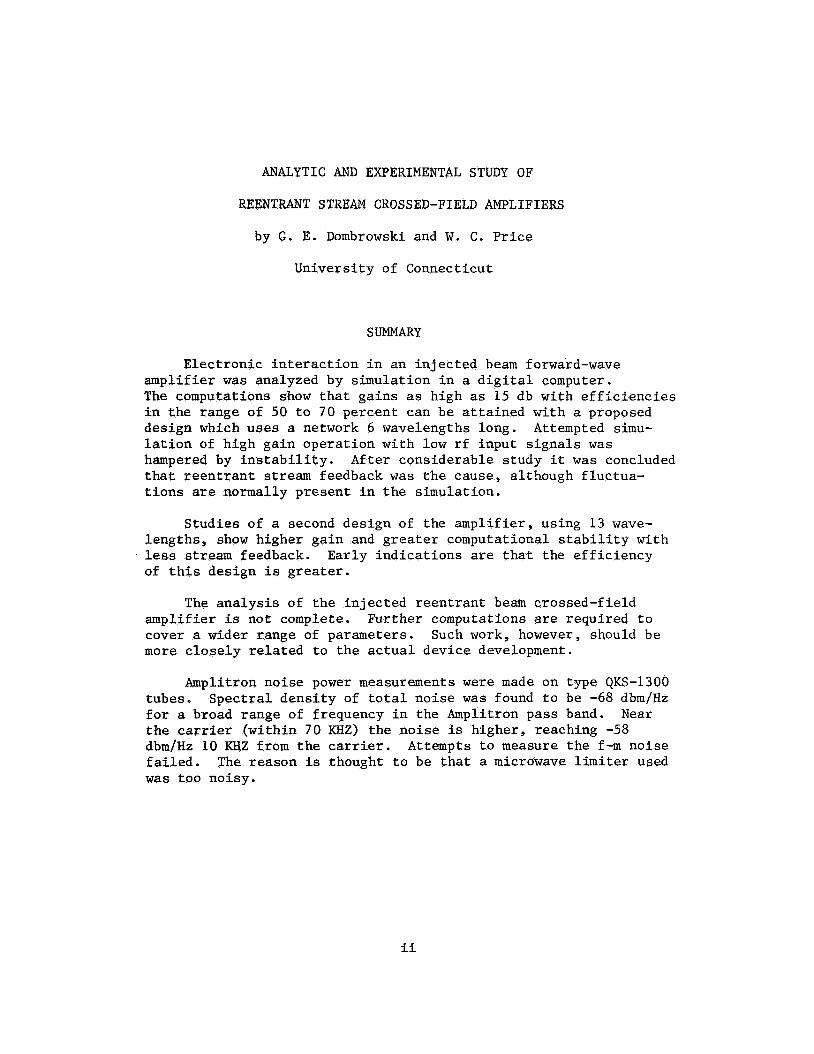
SUMMARY
Electronic in t e rac t ion i n an in jec ted beam forward-wave amplif ier w a s analyzed by simulation i n a d i g i t a l computer. The computations show t h a t gains as high as 15 db with e f f i c i e n c i e s i n the range of 50 t o 70 percent can be a t ta ined with a proposed design which uses a network 6 wavelengths long. Attempted simu- l a t i o n of high gain operat ion with low r f input s igna ls w a s hampered by i n s t a b i l i t y . t h a t r een t r an t stream feedback w a s t h e cause, although f luctua- t i o n s are normally present i n the simulation.
After considerable study it w a s concluded
Studies of a second design of the ampl i f ie r , using 13 wave- lengths , show higher gain and g rea t e r computational s t a b i l i t y with less stream feedback. Early ind ica t ions are t h a t the e f f ic iency of t h i s design is grea te r .
The ana lys i s of t he in jec ted reent ran t beam crossed-field amplif ier is not complete. Further computations are required t o cover a wider range of parameters. more c lose ly r e l a t ed t o the a c t u a l device development.
Such work, however, should be
Amplitron noise power measurements were made on type QKS-1300 Spect ra l dens i ty of t o t a l no ise w a s found t o be -68 dbm/Hz tubes.
f o r a broad range of frequency i n the Amplitron pass band. t h e carrier (within 70 KHZ) the noise is higher, reaching -58 dbm/Hz 10 KHZ from the carrier. Attempts t o measure the f-m noise f a i l e d . The reason is thought t o be t h a t a microwave limiter used w a s too noisy.
Near
ii
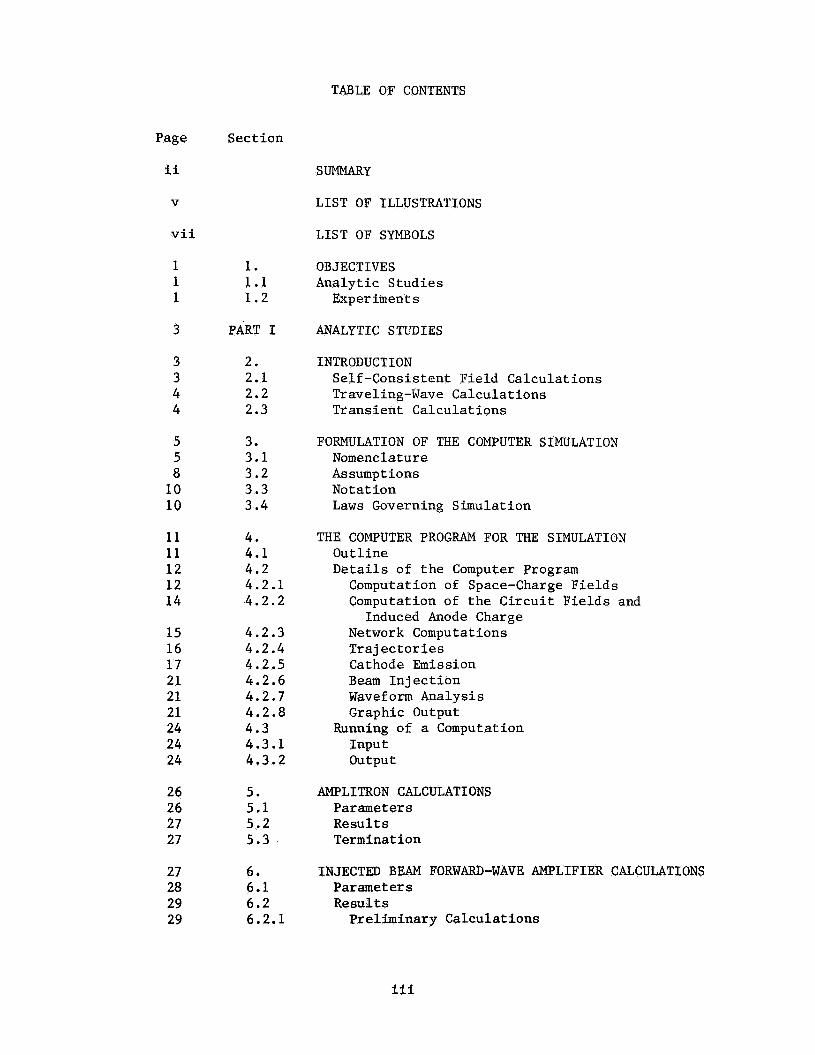
TABLE OF CONTENTS
Page
ii
V
v i i
1 1 1
3
3 3 4 4
5 5 8
10 1 0
11 11 1 2 12 1 4
15 16 17 21 21 21 24 24 24
26 26 27 27
27 28 29 29
Sect i o n
1. 1.1 1 . 2
PART I
2 . 2.1 2.2 2.3
3. 3.1 3.2 3 .3 3 .4
4 . 4.1 4.2 4.2.1 4.2.2
4.2.3 4.2.4 4.2.5 4.2.6 4.2.7 4.2.8 4.3 4.3.1 4.3.2
5 . 5.1 5.2 5.3
6 . 6.1 6.2
SUMMARY
LIST OF ILLUSTRATIONS
LIST OF SYMBOLS
OBJECTIVES Analytic S tud ie s
Experiments
ANALYTIC STUDIES
INTRODUCTION Self-consis tent Field Calculat ions Traveling-Wave Calculat ions Transient Calculat ions
FORMULATION OF THE COMPUTER SIMULATION Nomenclature A s sump t ions Not a t ion Laws Governing Simulation
THE COMPUTER PROGRAM FOR THE SIMULATION Out l i n e Details of t h e Computer Program
Computation of Space-Charge F i e l d s Computation of t h e C i r c u i t F i e l d s and
Network Computations T r a j e c t o r i e s Cathode Emission Beam I n j e c t i o n Waveform Analysis Graphic Output
Input
Induced Anode Charge
Running of a Computation
Output
AMPLITRON CALCULATIONS Parameters Result s Terminat i o n
INJECTED BEAM FORWARD-WAVE AMPLIFIER CALCULATIONS Parameters Resul ts
6.2.1 Prel iminary Calculat ions
iii
TABLE OF CONTENTS (cont . )
Page
31 31 42 47 47 47 51 51 57
59 59 59
64
64
64 64 64 66 68
72
72 72 76 8 2 84 86 90 98
103 106 109 116
119
Sect ion
6.2.2 6.2.3 6.3 6.4 6.4.1 6.4.2 6.4.3 6.4.4 6.5
7. 7.1 7.2
PART I1
8.
9. 9.1 9.2 9.3 9.4
APPENDIX
A. A. 1 A. 2 A. 3 A. 4 A.5 A. 6 A. 7
A. 8 A. 9 A. 10 A . l l
Demodulation & Feedback Through t h e Stream I n s t a b i l i t y a t High Gain
Amplifier Performance a t Moderate Gain Ef fec t of Parameters on Operation
D c Anode Voltage D e In j ec t ed Current Rf Input Power Level Rf Impedance Level
Second Design of t he In j ec t ed Beam Amplifier
CONCLUSIONS OF ANALYTIC STUDY Conclusions Recommendat i ons
AMPLITRON NOISE MEASUREMENTS
INTRODUCTION
MEASUREMENTS Scope Measurement Techniques Resul ts Conclusions
COMPUTER PROGRAM LISTING Control Program Input Program Space-Charge Green's Function Anode Green's Function Graphic Display Space-Charge F ie ld Calculat ion Induced Charge, Network Response, & C i r c u i t
Cathode Emission Tra j ec to ry Calculat ions Merge, Co l l ec t and Output Fourier Analysis
F i e l d s
DISTRIBUTION LIST
i v
LIST OF ILLUSTRATIONS
Page
6 7 9
18 19 20 22 23
30
32 34
35
36 37 39
40 41 .4 3
44 45 46 48
49 50
52 53 55 56 58 60 61 62 65
Figure No.
3.1 3.2 3.3
4.1 4.2 4.3 4.4 4.5
6.1
6.2 6.3
6.4
6.5 6.6 6.7
6.8 6.9 6.10
6.11 6.12 6.13 6.14
6.15 6.16
6.17 6.18 6.19 6.20 6.21 6.22 6.23 6.24 9.1
Title
Interaction Space Nomenclature Lumped Constant Network Models Phase Characteristics of Networks of Figure 3.2
Construction for Trajectory Calculation Test Calculations of Electron Orbit in Static l/r Field Net Cathode Emission as a Function of Cathode Field Specimen of Graphic Display for Amplitron Calculation Specimen of Graphic Output (Injected Beam Amplifier)
Extension of CFA Calculation t010268: Failure to Reach Steady State
Example of Instability Calculation #6012: Space-Charge Forces Omitted;
Standing Wave Resulting from Mismatch of Amplifier.
Calculation Carried for Extended Period Spectrum Analysis of Output Voltage Waveform Transition from Uniform DC Drift Potential to Tapered
Variation of Length of Drift and Active Sections Drift Section Removed Comparison of Calculations With and Without Stream Reentrance
Calculation 86007: Configuration at T-96.0 Calculation f6007: Configuration at T-96.5 Calculation #6007: Configuration at T=97.0 Distribution of Current and Voltage on Network;
Calculation #6007: Collector Histogram RF Current Distribution as Function of Injected
Effect of Injected Current on Performance RF Current in Stream vs. RF Drive Power Power Transfer Characteristic Start-up Transient with Very Small RF Input Signal Calculation #7004: Internal Voltage Distribution Calculation f5010: Configuration at T-40.8 Calculation #5010: Configuration at T-41.2 Calculation #5010: Configuration at T-41.8 Amplitron Noise Measuring Bridge System
Artificial Stream Demodulation
Reflection Coefficient: 1/3
Drift Potential
Calculation #6007, T-97.0
Cur rent
V

Page Figure No.
67 9 - 2 69 9 . 3 70 9 . 4 71 9.5
LIST OF ILLUSTRATIONS (Cont.)
T i t l e
E f f e c t of Heater Current on Noise Noise Power as a Function of RF Drive Power F-M Noise Power Density Measurement : "Cold" Tube F-M Noise Power Density Measurement: Operating Tube
v i
LIST OF SYMBOLS
SYMBOL PAGE
ACF 25 B 11
28 BO
C C’
$9 E -1
9 ‘b 9 cc
‘nn, ‘run cO
cl’ c2 I1) I2
G GAP 3i
ht
IC Ii (N)
h
‘b
11 16 16 7 15 10 7 7 7
26 26 11 16 11 12 24 15 10 7
16 6 16 10 26 26 48
CORRESPONDING COMPUTER VARIABLE
ACF
CA , CB CC
61; c2 CINl , CIN2 COUTl,COUT2 CNS T
EX, EY
GA,GB ,GC
G1, 62
GAP HT
DESCRIPTION
Autocorrelation function Magnetic flux density Critical (sca1ing)magnetic
Capacitance element Effective capacitance Capacitance matrix inverse Network capacitance elements Self, mutual capacitances Scaling capacitance parameter Network terminating capacitances Network source currents Network source currents Emitted charge element Anode diameter Cathode (sole) diameter Electric field components Initial values of EX, EY Conductance element Green’s functions Network conductance elements Self, mutual conductances Scaling conductances Network terminating (load)
Conductance matrix Fractional intervane spacing Time increment Axial length of interaction space Dc anode current Dc collector current Induced current of Nth electrode
flux density
conductances
vii
LIST OF SYMBOLS (cont .)
S m O L
'k
I n
I O
5' I 2 I
J - JS
KO k k 0
LO NE NG
NK PS
'in Pout P
QO r r -
PAGE
28
15
10
7
16
20
20
28 16
10
10
5
5 21
24
10
28
26
24
24
11
14
14
53
10
6
12
10
CORRESPONDING COMPUTER VARIABLE
NE
NG
NK PS
P
PIN
PD
PDIN
Q
DESCRIPTION
D c i n j ec t ed (cathode) cu r ren t
Current i n t o Nth e l ec t rode
Scal ing cu r ren t
Source cu r ren t s
Cur r e n t mat r ix
Current dens i ty
Sa tu ra t ion emission cu r ren t d e n s i t y
Coupling impedance, EE*/2B2P
Boltzmann constant
Reference mode number
Scal ing inductance
Number of anode s e c t o r s
Number of a c t i v e anode s e c t o r s
Number of emission sites
Normalized mean particle diameter
Scaling power
Signal input power
Signal output power
Radial coordinate; p-0 is cathode ( so l e )
I n j e c t i o n r ad ius
Radial v e l o c i t y
I n j e c t i o n r a d i a l v e l o c i t y
Normalized charge
Induced charge a t Nth e l ec t rode
P a r t i c l e charge
Amplitude of s i g n a l frequency
Scal ing charge
Radial coordinate
Pos i t i on vec tor
Anode r a d i u s
component of Qi(N)
r a
v i i i
LIST OF SYMBOLS (cont . )
SYMBOL
r
r
'k
C
S
S
S
S
S
- i
0 T
T
t
U - u u x' Y
V
V '
' vo
'b
PAGE
10
6
14
11
11
11
6
11
16
11
11
11
10
11
10
26
14
26
11
15
15
32
16
16
26
16
11
7
15
CORRESPONDING COMPUTER VARIABLE
sz T
trx, UY
VDC
VDD
GAMA, GAMB , GAMC
DESCRIPTION
Cathode (so le ) rad ius
Sole rad ius
Surface of k th e lec t rode
Normalized rad ius
Pos i t ion vector (normalized)
I n i t i a l pos i t ion vector
Normalized cathode (so le ) radius
Normalized t i m e , v t
Temperature
Real t i m e
Normalized ve loc i ty vec tor
Velocity components
Electric p o t e n t i a l
T i m e de r iva t ive of e lectr ic
Scaling vol tage
Anode vol tage
D c d r i f t sec t ion vol tage
Ci rcu i t component of po ten t i a l
Average co l l ec to r po ten t i a l
Hartree vol tage
RF po ten t i a l of nth, mth e lec t rodes
Time de r iva t ives of Vn and V
Amplitude of r-f vol tage on n t h
Voltage matrix, time-derivative
Exci ta t ion matrix
Anode vane width
1/(2~lkT)=11600/T
Reciprocal inductance
Network inductance elements
Se l f , mutual inductance parameters
p o t e n t i a l
m
e lec t rode
ix

LIST OF SYMBOLS (cont.)
SYMBOL
E
n 0
8
0 '
'rn 0
mP O0
8S V
0
P
w
u 0
PAGE
10
24
16
12
10
10
5
24
17 24
24
11
6
10
10
24
20
9
CORRESPONDING COMPUTER VARIABLE
GL1, GL2
TH
THQ
THDIN
THM
THMP
THS
TLIFE
DESCRIPTION
Scaling rec iproca l inductance
Network terminating inductances
Inductance matrix
Dirac d e l t a funct ion
Free space d i e l e c t r i c pe rmi t t i v i ty
Magnitude of e l ec t ron spec i f i c
Azimuthal coordinate
Azimu t ha1 t i m e ra t e ( "velocity 'I)
Azimuthal ve loc i ty of in jec ted
Increment i n azimuth
Range of space chargeGreen's fcn.
Range of anode Green's fcn.
Cyclotron t i m e , w t
Azimuth of one sec tor
Reference frequency
Normalized charge dens i ty
Electron axial t r a n s i t t i m e
Electric po ten t i a l
Frequency
Reference (angular) frequency, 21rv.
charge
C
X
1. OBJECTIVES
1.1 ANALYTIC STUDIES
1.1.1 General Objectives
The general objectives of this phase of the research are the develop- ment and application of a computer model to the study of high-efficiency, high power crossed-field amplifiers using reentrant electron streams.
The operational characteristics of the amplifier of interest are:
a. Gain; b. Output; c. Efficiency; d, Bandwidth; e. Linearity; f. Phase distortion.
A determination is to be made of how these characteristics are affected by such operating variables and design parameters as
a. b.
d. e. f. g* h. i.
C.
j-
dc magnetic field intensity; dc anode voltage dc anode current; rf input level; rf interaction space length; rf network impedance; rf network phase characteristics; rf network attenuation; number and shape of anode electrodes; length of demodulation (drift) section, if any.
1.1.2 Specific Objectives
Originally, the amplifier device on which calculations were to have been made was the Amplitron. beam derived by thermionic or secondary emission from a cylindrical cathode. Its rf network encompasses the entire perimeter of the inter- action region (there is no drift region), but is itself not reentrant. may be thought of as the result of severing the straps of a conventional strapped-vane magnetron.
This crossed-field amplifier uses a reentrant
It
Inasmuch as Amplitrons have been well understood and in widespread use for many years, and also because a computer program for its large- signal analysis had been in existence, these computations take on the nature of the collection of a body of information for design refinement.
Subsequently, however, the application for which the’hplitron was intended was modified to the extent that the Amplitron was no longer desired. different reentrant-stream crossed-field amplifier.
It was replaced in the intended application and this study by a The new device uses
-1-
a forward-wave network, has a demodulating sec t ion , and obta ins i t s elec- t ron stream by axial i n j e c t i o n of a hollow beam. The scope of t he study therefore i s extended t o consider t h e e f f e c t s of i n j e c t i o n parameters on the ampl i f ie r performance.
The new form of amplif ier is a t an e a r l y s tage of development, how- ever. The a p p l i c a b i l i t y of t he computations thus t o some degree takes on the charac te r of point ing out t h e d i r ec t ions f o r f u r t h e r device develop- ment r a the r than design refinement.
1 . 2 EXPERIMENTS
1.2.1 Amplitron Performance
I n conjunction wi th t h e numerical ana lys i s , measurements were t o have been made, e spec ia l ly a t high magnetic f i e l d s and with such parameters as indicated by computer r e s u l t s , on a commercial Amplitron of medium power. The objec t ive of t h i s phase w a s t o v e r i f y as much of the computer optimi- za t ion as possible .
When t h e Amplitron w a s discarded as a candidate f o r the appl ica t ion as the t ransmi t te r tube, t h i s phase of t he pro jec t w a s abandoned.
1.2.2 Amplitron Noise Measurements
A s a separa te i s sue , measurements w e r e t o be made of t he noise inherent i n the Amplitron as a t ransmi t te r tube f o r general appl icat ion. The t o t a l noise w a s t o be measured as a funct ion of frequency r e l a t i v e t o the amplified s igna l , and w a s t o have been resolved i n t o i t s f-m and a-m components.
-2-

PART I. ANALYTIC STUDIES
2. INTRODUCTION
There is a clear need f o r information with which t o optimize t h e design of high power microwave tubes. of such highly e f f i c i e n t ones as crossed-field devices, s ince the d i s s i p a t i o n within t h e device--and consequent heating and heat d i s - s i p a t i o n problems--is more r a d i c a l l y a f fec ted by a given change i n e f f i c i ency f o r them.
This is e spec ia l ly t r u e
Because high power devices inev i t ab ly involve nonlinear i n t e r - Large capacity, ac t ions , numerical ana lys i s is usua l ly necessary.
high speed computers are r e a d i l y ava i l ab le f o r t h i s purpose. The primary l i m i t a t i o n involved i n r e s o r t t o numerical work i s the d i f f i c u l t y i n making genera l iza t ions t h e s p e c i f i c cases studied.
The computers present ly ava i l ab le are a t t r a c t i v e instruments fo r making simulations of a wide v a r i e t y of complex systems, of which the microwave e l ec t ron device i s su re ly a member. Such computer experi- ments are much cheaper t o run than tests on a c t u a l high power tubes. Parameter changes can be more e a s i l y made i n t h e computer, and the r e s u l t s thereof more r ead i ly discerned. The computer, however, i s l imi ted by t h e v a l i d i t y of the model used t o represent t he real device.
2.1 Self-consistent Field Calculations
Some of the earliest numerical ana lys i s of e l ec t ron tubes w a s t h e app l i ca t ion t o t h e magnetron of Hartree's method of se l f -cons is ten t f i e l d s , below:
I n i t s use here, the ca l cu la t ions proceed somewhat as outlined
a. The space-charge configuration is assumed (by guess--educated o r otherwise) ;
b. t h e electric p o t e n t i a l of t h e i n t e r a c t i o n region is computed from the space-charge and the applied r f and dc po ten t i a l s . This is t h e so lu t ion of Poisson's equation;
c. e l ec t ron t r a j e c t o r i e s are computed from the cathode i n t h i s f i e l d ;
d. t he cu r ren t s ca r r i ed on each t r a j e c t o r y are adjusted so t h a t t h e p o t e n t i a l g rad ien t at the cathode is zero. l imi ted conditions are thus assumed;
Space-charge-
e. t h e r e s u l t i n g t o t a l space-charge configuration is compared with t h a t from which it w a s derived. I n a series of itera- t i o n s , new configurations are generated with which t o repeat t h e sequence out l ined above.
According t o t h e simple theory of t he Amplitron, t he space-charge i s very much l i k e t h a t i n t h e magnetron i n s p i t e of t h e ampl i f ica t ion of t he r f s igna l with azimuth. The reasons f o r t h i s are the absence
-3-

of a d r i f t region t o allow f o r debunching and t h e r a the r sho r t recir- cu la t ion t i m e of t h e e lec t rons . A good se l f -cons is ten t f i e l d calcula- t i o n would thus be a s t a r t i n g point fo r Amplitron ana lys i s .
The success of t h e se l f -cons is ten t method obviously depends on one's a b i l i t y t o make w i s e guesses of the space-charge. r equ i r e s freedom from i n s t a b i l i t y i n t h e sense t h a t small devia t ions from the co r rec t answer must not lead one i n t o making guesses t h a t are even. wilder. success. charge, i t s consequent e f f e c t on the electric f i e l d , and the c r i t i c a l dependence of the e l ec t ron paths of t he e l e c t r i c f i e l d through the pa r t i a l balance of t h e Lorentz force . There is , indeed, considerable doubt whether the magnetron is r e a l l y a s t a b l e device.
It a l s o
Unfortunately, previous workers i n t h i s area have not m e t The underlying cause seems t o be the presence of dense space-
2.2 Traveling-Wave Tube Calculations
Subsequent t o t h e invention of t he traveling-wave tube by Kompfner 0 and t h e development of an elegant s m a l l s i gna l theory by Pierce , large-
s igna l computer s tud ie s were made. A t t h a t t i m e computers w e r e i n a very e a r l y s t age of development, and many approximations w e r e made i n order t o ge t so lu t ions . One of t hese is t h a t i n t e r a c t i o n takes plgce only with the c i r c u i t component wave t rave l ing i n near synchronism with t h e e lec t rons . This i s reasonable only with in j ec t ed beam devices such as the 0-type t r ave l ing wave tube and the in j ec t ed beam c l a s s of crossed- f i e l d ampl i f ie rs (non-reentrant). It does not seem t o be appl icable t o the Amplitron, which has important nonsynchronous components and a multi- ve loc i ty stream. Another assumption i s t h a t of s m a l l ga in rate, which
v a r i a t i o n from one bunch t o the next and an ove ra l l ca l cu la t ion as an in t eg ra t ion pass from input end t o output end of the system. I n such crossed-field devices as the Amplitron and o ther emitt ing s o l e tubes, t he gain rate is q u i t e high and space-charge fo rces canzlot be computed t h i s way. Moreover, stream reentrancy without demodulation makes i t impossible t o know t h e conditions at the input end of the system u n t i l t h e output conditions are determined. t o be q u i t e appl icable t o handling t h e forward-wave CFA with the in jec ted beam.
. allows t h e computation of space charge fo rces without regard t o the
This method, nevertheless appears
2.3 Transient Calculations
The se l f -cons is ten t f i e l d technique not only f a i l s i n the case of t he magnetron, but as with a l l iterative methods, t h e intermediate s tages f a i l t o y i e ld any phys ica l ly meaningful r e s u l t s . method one attempts t o simulate a physically poss ib le s i t u a t i o n , such as t h e s ta r t -up of an o s c i l l a t o r , and then t o follow i t s development i n t o steady state. It e l imina tes t h e need t o guess a t any charge configura- t i on . Rather one starts with, say, no charge at a l l , from which one computes the f i e l d s , thence t h e emission, and the r e s u l t i n g charge con- f i g u r a t i o n a very sho r t time later. are then computed, and t h e ca l cu la t ion marches on with time.
IR the t r ans i en t
The f i e l d s of t h e new configuration
-4-
Transient ca l cu la t ions had been made during the course of e a r l y magnetron research t o determine the s ta t ic d i s t r i b u t i o n i n t h e cut- o f f magnetron. The extension t o include time-varying f i e l d s has been made only recent ly .
I n the case of t he Amplitron and other crossed-field ampl i f i e r s , t h i s technique appears t o be q u i t e promising--assuming t h a t steady state i s reached, as it has i n many cases. An add i t iona l f a c t o r involved i n ampl i f ie rs i s t h e v a r i a t i o n of space-charge and c i r c u i t f i e l d s from spoke t o spoke and with d i s t ance along t h e s igna l path. This can be handled i n modern computers without t h e r e s t r i c t i o n s of t he pas t t o only one o r a few Hartree (space) harmonics. Indeed, t he t r a n s i e n t ca l cu la t ion may properly be regarded as a case of simulation of both the stream and the network i n the computer.
The t r a n s i e n t ca l cu la t ion , o r more genera l ly , computer simulation i n the t i m e domain, is the method t h a t w a s applied t o previous ana lys i s of t he Amplitron. It i s used i n the present research and is described f u l l y i n Section 4 .
It must be remembered, however, t h a t t h e magnetron and r e l a t ed crossed-field devices are c r i t i c a l l y dependent on space charge and on t h e balance between e l e c t r o s t a t i c and Lorentz fo rces f o r focusing. The se l f -cons is ten t f i e l d ca l cu la t ions f a i l e d because of these f a c t o r s , i .e., because the ca lcu la ted e l ec t ron paths did not go where t h e elec- t rons w e r e supposed t o have been. I n the computer simulation t h i s is not a problem: t h e e l ec t ron pos i t ions are known, and t h e i r e f f e c t s on the f i e l d s are known. a t t a i n i n g a steady state and i n the f luc tua t ions and/or o s c i l l a t i o n s therefrom. To some extent t he determination of steady state r e s u l t s i s a s ta t is t ical problem because of t he f luc tua t ions . It i s expected t h a t i f a l a r g e enough system of p a r t i c l e s is used t o simulate t h e ac tua l e l ec t ron stream, these f luc tua t ions w i l l be s m a l l . This c e r t a i n l y depends on t h e inherent s t a b i l i t y of t he system under simulation.
The d i f f i c u l t y of t he ca l cu la t ion appears i n
3. FORMULATION OF THE COMPUTER SIMULATION
3 .1 Nomenclature
Figure 3.1 shows t h e nomenclature of t h e i n t e r a c t i o n region. I n t h e computer it is poss ib le t o keep account of a l a rge number of var i - ab les , hence the e lec t rodes are numbered, s t a r t i n g with #l a t 8=0,and proceeding counterclockwise t o #NE. Of these e lec t rodes , the f i r s t NG are active; t h e remainder have only d-c p o t e n t i a l s as a d r i f t section. I n the Amplitron, NG=NE, i .e., t h e r e i s no d r i f t section. The r-f s igna l is applied a t f l f o r a backward-wave network, as most Amplitrons use, and propagates counterclockwise. The e l ec t rons move i n the clock- w i s e d i r e c t i o n with pos i t i ve anode vol tage and a x i a l magnetic f i e l d .
Figure 3.2(a) shows t h e r f network typ ica l of Amplitrons.
A balance-to-unbalance t r a n s i t i o n is usua l ly connected t o the
It i s e s s e n t i a l l y a balanced two-wire l i n e ( the s t r aps ) with resonator (vanes) loading. ends of t h e network t o transform t o t h e ex te rna l s igna l paths. Figure
-5-

6
F i g u r e 3.1. I n t e r a c t i o n S p a c e N o m e n c l a t u r e .
-6-

a. Network for Amplitrons (strapped vanes).
b. Forward-wave network.
Figure 3.2, Lumped constant network models. Electrode numbers in brackets.
-7-
3.3(a) shows t h e phase c h a r a c t e r i s t i c of such a network.
Figure 3.2(b) shows an elementary forward-wave network used t o simulate t h e in j ec t ed beam, forward-wave ampl i f ie r . t h e network used i n the a c t u a l tube are not known, but t h i s represen- t a t i o n i s considered t o be t h e bes t known one inasmuch as i t s d ispers ion i s minimal.
Precise d e t a i l s of
Its phase c h a r a c t e r i s t i c is shown i n Figure 3.3(b).
The ana lys i s of t he in jec ted beam forward-wave device is based on Figure 3 .1 wi th t h e spec i f i ca t ion t h a t e l ec t rons are emitted a t some intermediate r ad ius and have clockwise angular ve loc i ty . The s igna l input i s a t t h e NGth e lec t rode ; propagation i s a l s o clockwise, t h e load being connected t o the f i r s t electrode.
3.2 Assumptions
The following assumptions are made:
a. b.
d. e. f . g * h. i.
C.
3 .
The dc magnetic f i e l d i s uniform and axial. Cathode is c i r c u l a r cy l inder concentric with t h e anode. A l l anode e lec t rodes are i d e n t i c a l and equally spaced. Al l network elements are i d e n t i c a l and idea l . Cathode emission i s uniform. Electron motion i s n o n r e l a t i v i s t i c . No n e u t r a l o r ionized gas atoms are present. Electric f i e l d r e t a rda t ion e f f e c t s are negl ig ib le . R€ magnetic f i e l d fo rces are negl ig ib le . No secondary e l ec t ron emission takes place.
These are the bas ic assumptions necessary f o r expeditious handling of microwave tube problems. It is of course necessary t h a t t h e network representa t ion used be a realist ic model f o r t h e a c t u a l microwave network; t h i s i s a matter of degree of approximation.
I n the be replaced
(e)
ana lys i s of t h e in j ec t ed beam device, assumption (e) i s t o by
i n j e c t i o n takes p lace equal ly a t equally spaced sites located on the i n j e c t i o n circle. same axial ve loc i ty , which i s such t h a t a f t e r TLIFE r f cycles they emerge from t h e i n t e r a c t i o n process and are eliminated therefrom;
Al l in jec ted e lec t rons have t h e
I n addi t ion t o t h e bas ic assumptions made above are added t h e s p e c i f i c assumptions below, which are subjec t t o modification as t h e problem changes o r t h e model. improves:
a. A l l anode e lec t rodes are i d e n t i c a l and equally spaced. They have circular inner f aces and r a d i a l s ides . The f i e l d i s assumed to be purely azimuthal between r a d i a l f aces of adja- cen t e lec t rodes ;
Other r e s t r i c t i o n s i n t h e model take on t h e na ture of t h e approxi- mations made; they w i l l be described i n connection with t h e s p e c i f i c
-8-

0 3 \ 3
h
a , . 7 -- 0- a, k L
g 1
0 0 k0 Mode number, k
a. Amplitron network (strapped varies)
b. Forward-wave Network
Figure 3.3. Phase Characteristics of Networks of Figure 3.2.
-9-
por t ions of t h e a n a l y s i s below.
3 . 3 Notation
3 . 3 . 1 I n t e r a c t i o n Space Geometry
As indicated i n Figure 3.1, t h e following nota t ion appl ies :
r Anode r ad ius
r Sole r ad ius
so Ratio: s o l e radius/anode r ad ius h Axial length of i n t e r a c t i o n system GAP Fraction of anode circle f o r intervane gap NE Number of anode e lec t rode sec to r s NG Number of active anodes
a
C
3 . 3 . 2 Normalization
For re ference purposes only, a re ference frequency and mode number are defined. va lue , which i s t h e e l ec t ron k i n e t i c energy f o r synchronism i n t h e re ference mode a t re ference frequency. This vo l tage is described i n Table 3 . 1 . A re ference capacitance, cu r ren t , Io, is t h e r f cur ren t flowing through Co with Vo applied a t frequency vo.
Voltages are normalized with respect t o t h e synchronous
is a l s o l i s t e d . The re ference cO *
Other sca l ing va lues follow.
Table 3 . 1 Normalizing Variables
Vo 1 t age Capacitance Charge Current Power Conductance Inductance l /Inductance
VO CO Qo IO PO GO LO f 0
3.4 Laws Governing Simulation
The l a w s t h a t govern t h e computer model are mainly t h e same as those of a physical system: Poisson's, Newton's, and Kirchoff 's .
I n t h e computer model, using normalized po ten t i a l , charge, and d is - tance, Poisson's Law takes t h e form
v2v = P, (3 1 )
where t h e Laplacian operation i s i n t h e normalized coordinate system. The charge dens i ty P i s p o s i t i v e f o r e l ec t rons (it i s l i k e a number den- s i t y ) , accounting f o r t h e odd a lgeb ra i c s ign of t h i s equation.
-10-
I n dealing with t h e equations of motion i n t h e computer i t is convenient t o de f ine a v e l o c i t y v a r i a b l e which is d i r e c t l y commensu- rate wi th t h e electric f i e l d . This is done with t h e machine veloci- ties
UY = u (raB/Vo); UX = u (raB/Vo) Y X (3.2)
Then, using normalized electric f i e l d s and cyclotron time, 8O-w t Newton's n o n r e l a t i v i s t i c equations become C
dUY - - m + u x deo
dUX - = E X - U Y de O
Normalized d i s t ance along a t r a j e c t o r y i s
2 s - s = [-y) 1 wo l 2 d e o - i 2 k w - (3 -4)
and k i n e t i c energy of a charge is, normalized t o QoVo, 2
K . E . = Q [&] {UX2 + W2}
and k i n e t i c energy of a charge is, normalized t o QoVo, 2
K . E . = Q [&] {UX2 + W2}
The Kirchoff node equations are q u i t e straight-forwardly scaled i n terms of charge, admittance elements, and t i m e , t o y ie ld equations of t h e type
I = GV + CV' + FlVdT,
where t h e prime denotes t h e de r iva t ive with respec t t o normalized time, Tgv t. 0
For reference purposes, t h e Hartee voltage i n the normalized system is
VH ko-(l w - so) 2 - 1 @ O
(3.7)
Aside from some assumed l a w of emission (cathode f o r Amplitrons; i n j e c t i o n f o r t h e in j ec t ed beam device), these th ree l a w s are the only ones b u i l t i n t o t h e computer model. t h e mode number ko are s o l e l y f o r reference; nothing is assumed as t o t h e frequency o r mode of i n t e rac t ion , i f indeed t h e r e is any.
The use of t h e frequency vo and
4. The Computer Program f o r t h e Simulation
4.1 Outline
The t r a n s i e n t ca l cu la t ion has t h e following steps:
1. The space-charge fo rce between each e l ec t ron and a l l o the r s
-11-
2 . 3 .
4 .
5.
6.
7.
8.
is ca lcu la ted ; The induced charge on each e lec t rode is ca lcu la ted ; From t h e previously known induced charge, t h e induced cu r ren t s are ca lcu la ted . With t h i s information and the network v a r i a b l e s and parameters, t h e new network r f vo l tages are ca lcu la ted ; From t h e r-f vo l tages and t h e d-c vol tages , t h e c i r c u i t f i e l d fo rces on each p a r t i c l e are ca lcu la ted . added t o t h e space-charge fo rce t o g e t t h e t o t a l electric force ; From t h e known e l ec t ron v e l o c i t y a t t h e beginning of t h e time s t ep and t h e electric force , t h e t r a j e c t o r y i s computed a t t h e end of t he next time step; From t h e known electric f i e l d a t t h e cathode t h e cathode thermionic emission i s computed; The emitted p a r t i c l e s are merged i n t o t h e set of a l l pa r t i c - les, in te rcepted p a r t i c l e s are eliminated, and t i m e is advanced one s t ep ; After p r in tou t of t h e intermediate r e s u l t s , t h e computation r e tu rns t o s t ep #l.
This i s
The above o u t l i n e governs t h e Amplitron ca lcu la t ion . For the injec- ted beam, s t e p #6 is replaced by computing new charges not dependent on r-f conditions. Charges are a l s o removed a f t e r expi ra t ion of t h e i r tran- sit ( l i f e ) through t h e i n t e r a c t i o n space. The problem with an in jec ted beam has some three-dimensional aspec ts . I n order t o treat it as a two- dimensional one, the a x i a l v a r i a t i o n of fo rces on an e l ec t ron during i t s t r a n s i t through t h e i n t e r a c t i o n are neglected. Details of t h e var ious s t eps i n the ca l cu la t ion process are given i n separa te sec t ions below. The program l i s t i n g is given i n Appendix A,
4.2 Details of t h e Computer Program
4.2 .1 Computation of Space-Charge F ie lds
The choice of t h e method f o r ca l cu la t ion of t h e space-charge f i e l d s i s a cri t ical one. I n most analyses, t h i s i s the most time-consuming por t ion of t h e program. I n crossed-field devices, t he r o l e played by space-charge forces i s not completely understood, yet i s heavily involved i n t h e performance of t h e device, e spec ia l ly when high power i s required.
The method used here i s t h e evaluation and summation of t h e binary fo rces between p a r t i c l e s . considered t o be pe r fec t ly c i r c u l a r cy l inders a t zero po ten t i a l . binary fo rce i s computed by taking t h e gradient of a Green's space-charge p o t e n t i a l function, defined by
For t h i s determination t h e anode and so le are The
V2G (r,~' ) = ZIT 6 (L-L' )
G(2,f ' ) = 0 on s=s ,1 0
( 4 . 1 )
where ;is t h e pos i t i on vec tor a t t h e point a t which t h e f i e l d i s t o be evaluated, and 2' is the pos i t i on vec tor of t h e source charge. Hence, t h e space-charge p o t e n t i a l of a charge element is t h e Green's function
-1 2-

mult ip l ied by t h e normalized charge, Q, of t h e source.
The Green's func t ion is one of t h ree va r i ab le s : t h e r a d i a l coordi- na t e s of source and observation poin ts , and t h e azimuth between them.
2 The Green's func t ion is needed N times f o r an ensemble of N charges. It would be completely impractical t o compute i t d i r e c t l y each t i m e i t is needed. f o r t h e mesh po in t s of a three-dimensional gr id covering the ranges of t he th ree va r i ab le s i n which the fo rce i s appreciable. ponents are computed when required by in t e rpo la t ion using t h e mesh poin t va lues of t he p o t e n t i a l .
The technique used here i s t o compute and s t o r e the func t ion
The gradient com-
This technique has t h e speed of t a b l e look-up and in t e rpo la t ion as developed f o r computers. arithmetic; t h e in t e rpo la t ion , a few f l o a t i n g poin t operations. These have been optimized f o r speed by machine-language programming (IBM 7040 MAP and IBM 360 Agsembler). The powerful i n s t ruc t ion set and r e g i s t e r s t r u c t u r e of modern computers make t h i s a t t r a c t i v e .
The t a b l e look-up involves storage address
The accuracy of t h i s method depends mainly on the accuracy of t h e Green's function, on the mesh s i z e , and on t h e in t e rpo la t ion formula used. ca lcu la t ion . The second is limited by machine storage capacity. The last factor--the use of simple o r complex in t e rpo la t ion methods-- a f f e c t s t h e execution t i m e during t h e simulation, and i s the most c r i t i c a l .
The f i r s t of these three i s r e l a t e d t o the t i m e spent i n "set-up"
The program f o r pre-computing t h e Green's functions i s based on an expansion of t h e source charge ( the Dirac d e l t a function i n Equation 4.1) i n a Fourier series i n azimuth. Although the series i s i n f i n i t e , a f i n i t e number of terms i s adequate i n view of t h e f a c t t h a t t h e charge t o be represented i s not a t r u e l i n e charge, but has f i n i t e s i z e . To each Fourier t e r m t he re i s a well-known and easily-computed po ten t i a l ; these are summed t o y i e ld t h e Green's function. is l i s t e d i n Appendix A.3; i t is ca l l ed SPACH.
The program t o do t h i s
When two e lec t rons are c lose t o each o ther t h e use of t he precom- puted Green's func t ions poses d i f f i c u l t i e s because of i t s logarithmic s ingu la r i ty . s o l e e lec t rodes i s ignored and t h e Green's function i s taken t o be i t s l imi t ing expression
I n handling t h i s s i t u a t i o n , t h e existence of t h e anode and
When two ' e lec t rons ' are so c lose t h a t t h e d i f f u s e charge groups which they represent a c t u a l l y are enmeshed, t h e average fo rce between t h e groups is diminished by comparison with the fo rce between l i n e charges. designated PS. t h e i n t e r p a r t i c l e f o r c e when the e lec t rons in t e rpene t r a t e one another.
I n t h e computer t h e average 'diameter' of an ' e lec t ron ' is This value is used t o compute a l i n e a r reduction of
Another consideration i n the ca l cu la t ion of space-charge fo rces concerns p a r t i c l e s j u s t a f t e r emission from t h e cathode, a t which time
-13-

i t behaves more as a curved shee t than a rod ( l i ne ) . then c a l c u l a t e s t h e space-charge f i e l d as t h a t between the sheet and i t s image i n t h e cathode, which is approximated by a plane surface.
The computer
The program f o r evaluating the space-charge fo rces under the above conditions i s a subroutine named COOL. It is wr i t t en i n IBM 360 Assembler language, as shown i n Appendix A.6.
4.2.2 Computation of t he Ci rcu i t F ie lds and Induced Anode Charge
The c i r c u i t components of t h e electric f i e l d s on the p a r t i c l e s are a l s o ca lcu la ted from Green's functions. I n t h i s case the Green's func t ion s a t i s f i e s t he equations
V2Gk(rJ = 0
1 on Sk
Gk = [0 on S , j#k ( 4 . 3 )
j
S i s the sur face of t he k th e lec t rode ; a l l o thers , including the s o l e k (cathode) are designated S I f , as i s assumed here, a l l e lec t rodes of t h e anode are i d e n t i c a l and equally spaced, t h e Green's functions are a l l a l i k e when a s u i t a b l e mul t ip l e of azimuthal s ec to r angle is used f o r ro t a t ion . is
j*
I n any case, t h e c i r c u i t p o t e n t i a l a t any poin t , r,
where t h e summation i s over a l l NE e lec t rodes and, i f necessary, t h e cathode (so le ) as w e l l .
The anode e lec t rode Green's functions serve another purpose i n t h e computation. which t h e induced charge on t h e k th e lec t rode is given by
Ramo's induced charge theorem is invoked, according t o
the summation being taken over a l l charges.
The c i r c u i t f i e l d s and the induced charges are computed by i n t e r - po la t ion from s tored mesh poin t values.
There is a number of methods t h a t can be used f o r t h e ca l cu la t ion of the Green's functions. Relaxation is q u i t e genera l ly applicable; i t would be used f o r i r r e g u l a r o r i r r e g u l a r l y spaced electrodes. In the present case, ca l cu la t ions were made f o r a simple anode shape: t h e inner faces of t he vanes are assumed t o be segments of t h e anode circle; the s i d e f aces are assumed t o be purely r a d i a l . Also, t h e p o t e n t i a l is assumed t o vary l i n e a r l y with azimuth from vane t i p t o adjacent vane t i p . The Green's func t ion a t t h e anode circle is completely spec i f ied . It can e a s i l y be resolved i n t o Fourier components i n azimuth, each term of which series can be extended inward toward t h e cathode (so le ) . Com-
-14-
plex v a r i a b l e theory could a l s o have been used. computing t h e e lec t rode Green's func t ion i s l i s t e d i n Appendix A.4.
The program f o r pre-
The program f o r using t h e precomputed Green's functions proceeds i n three s t e p s : (1) t h e induced charge i s computed; (2) new network p o t e n t i a l s are computed from induced and ex te rna l ly applied cur ren ts ; (3) t h e c i r c u i t f i e l d s are computed. These s t e p s are executed i n the sub-routine l i s t e d as Appendix A . 7 .
4.2.3 Network Computations
I n many numerical analyses i t is assumed t h a t t he e l ec t ron stream i n t e r a c t s primarily with t h e dc f i e l d s and t h e r f f i e l d of a synchro- nously t r ave l ing wave. This wave is only one of t h e several components r e fe r r ed t o by t h e term Hartree harmonic. It i s v a l i d where there is e s s e n t i a l synchronism over a long period of t i m e , i * e . , where t rave l - ing-wave i n t e r a c t i o n occurs and is predominant. This may not be a very good assumption however, even i n the traveling-wave tube, f o r i n the high-level regions the non-synchronous components (as p a r t of t he t o t a l wave) {Dow) are l a rge , and t h e i n t e r a c t i o n may be r a the r diode-like more than of a traveling-wave type. I n the emitting-sole crossed-field tube o r i n t h e magnetron, r f f i e l d s are present a t the cathode and influence emission as w e l l as beam-forming. It seems necessary t o account f o r a l l components of t h e f i e l d , both r f and dc here.
The computer program wr i t t en with t h e idea of simulation i n mind is pe r t inen t here. components more important than o the r s i s made. What i s assumed is f i r s t , that r e t a rda t ion e f f e c t s are neg l ig ib l e , and second, t h a t a lumped-constant network can be found t h a t reasonably w e l l resembles t h e a c t u a l one. ac t ion space dimensions are small i n comparison with the free-space wavelength. i n comparison with t h a t of l i g h t , and t h i s i s a c h a r a c t e r i s t i c f e a t u r e of crossed-field tubes. The second assumption is increasingly w e l l s a t i s f i e d with the networks being used with more r ecen t ly developed ampl i f ie rs .
No assumption of synchronism or s e l ec t ion of f i e l d
The f i r s t assumption i s c e r t a i n l y f u l f i l l e d when the i n t e r -
This is in tu rn t r u e when the e l ec t ron v e l o c i t i e s are small
The network equations are based on t h e nodal formulation of Kirchoff 's equations, i .e., on the cont inui ty of cur ren t . of t h e network, an anode e lec t rode , t he equation of cont inui ty may be
For each node
w r i t t e n
- I n - GnnVn + CnnVA + rnn'V,dT
+ H(GmVm + CmVA + rm/vmdT) ( 4 6 )
where t h e symbols G, C y and r h a v e t h e i r usua l meanings as normalized conductance, capacitance, and (l / inductance); where t h e subscr ip t nn denotes t h e self-parameter, and where the subscr ip t m denotes a mutual parameter. ing t h e node.
The term on the l e f t cons i s t s of impressed cu r ren t s enter- These cons is t of ex te rna l ly impressed cu r ren t s ( a t t h e
-15-
end nodes) and t h e e l ec t ron stream induced cur ren ts . applied cu r ren t i s assumed t o be s inusoida l , but no assumption is other- w i s e made as t o t h e time-variation of any network quant i ty . This allows t h e ca l cu la t ion of a l l components of s i g n a l s t h a t t h e i n t e r a c t i o n might generate, including harmonics, subharmonics, and cyclotron frequency phenomena.
The ex te rna l ly
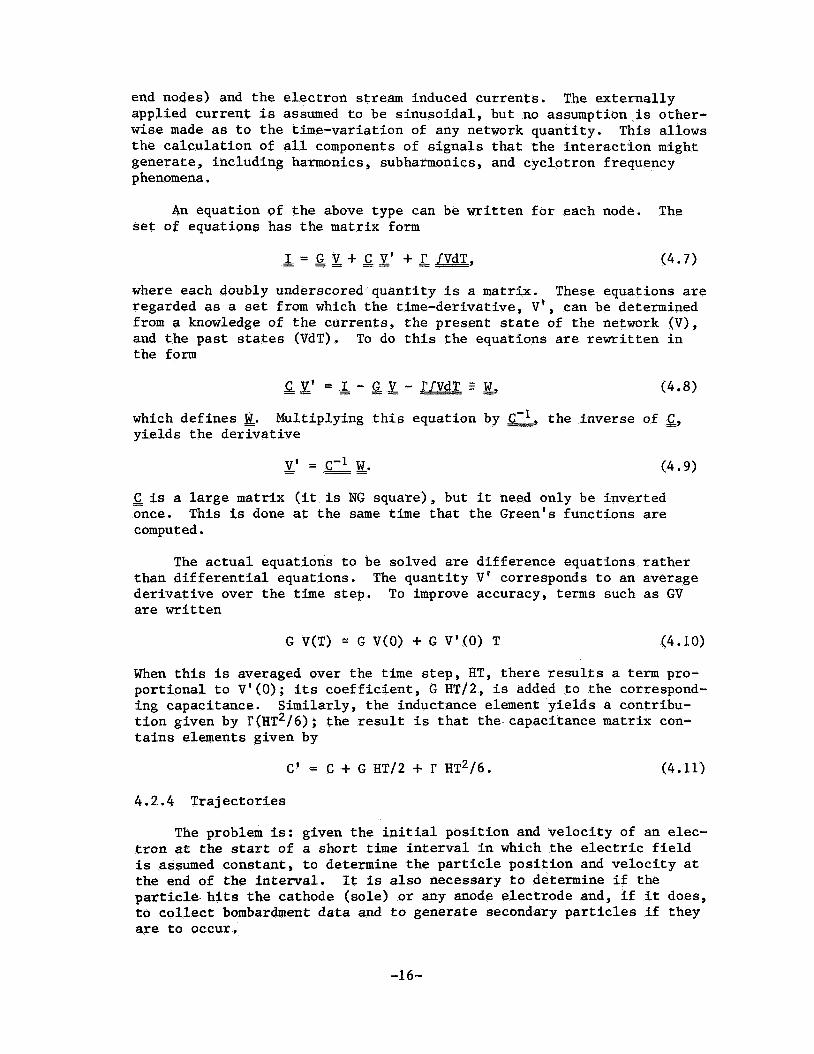
An equation of t h e above type can be wr i t t en f o r each node. The set of equations has t h e matrix form
- - I = GlJ+ -- CY' -- + - I? -9 JVdT (4.7)
where each doubly underscored quan t i ty is a matrix. These equations are regarded as a set from which t h e time-derivative, V ' , can be determined from a knowledge of t h e cur ren ts , t he present state of t h e network (V), and t h e p a s t states (VdT). t he form
To do t h i s t h e equations are rewritten i n
- -- C 1' = L - - G -- - - TfVdT E El, ( 4 8 )
which de f ines E. y i e l d s t h e de r iva t ive
Multiplying t h i s equation by c, t he inverse of s,
- - C i s a l a r g e matrix ( i t i s NG square), but i t need only be inverted once. This i s done at t h e same t i m e t h a t t he Green's functions are computed .
The a c t u a l equations t o be solved are d i f fe rence equations r a t h e r than d i f f e r e n t i a l equations. The quant i ty V ' corresponds t o an average de r iva t ive over t h e t i m e step. To improve accuracy, terms such as GV are wr i t t en
G V(T) G V(0) + G V'(0) T (4.10)
When t h i s i s averaged over t he t i m e s t ep , HT, t he re r e s u l t s a term pro- por t iona l t o V'(0); i t s coe f f i c i en t , G HT/2, i s added t o t h e correspond- ing capacitance. Similarly, t h e inductance element y i e lds a contribu- t i o n given by r(HT2/6) ; t h e r e s u l t i s t h a t t h e capacitance matrix con- t a i n s elements given by
C' = C + G HT/2 i- l' HT2/6. (4.11)
4.2.4 Tra jec to r i e s
The problem is: given t h e i n i t i a l pos i t i on and ve loc i ty of an elec- t ron a t the s ta r t of a shor t t i m e interval i n which t h e electric f i e l d is assumed constant, t o determine t h e p a r t i c l e pos i t i on and ve loc i ty a t t h e end of t he i n t e r v a l . It is a l s o necessary t o determine i f t he p a r t i c l e . h i t s t h e cathode (sole) o r any anode e lec t rode and, i f i t does, t o c o l l e c t bombardment d a t a and t o generate secondary p a r t i c l e s i f they are t o occur.
-16-
Some improvement became necessary f o r t h e t r a j e c t o r y ca l cu la t ion i n t h e course of t h e development of crossed-field programs. t h e t r a j e c t o r i e s could be computed as segments of cycloidal-trochoidal motion based on constant, uniform f i e l d s i n t h e time i n t e r v a l . is adequate i f t h e t i m e interval is small i n terms of cyclotron periods as w e l l as r f periods, and i f t h e f i e l d is t r u l y uniform. requirement is not m e t by a dc f i e l d i f t h e cathode has much curvature. It has been found that both t r a j e c t o r y and energy balance are l o s t i f t h e magnetic f i e l d is high enough t o make t h e time i n t e r v a l more than 1 / 4 cyclotron period even though t h i s may be only a much smaller f rac- t i o n of t h e r f period. where t h e r a d i a l f i e l d vector r o t a t e s along t h e t r a j e c t o r y i n the Cartesian frame f ixed r e l a t i v e t o t h e i n i t i a l point.
Previously,
This *
The last
This is p a r t i c u l a r l y t r u e near a small cathode,
A s shown i n Figure 4 .1 , a fixed Cartesian coordinate system is set up at t h e i n i t i a l po in t , P, a t t h e beginning of a time s tep . electronAmoves along i t s t r a j e c t o r y t o some poin t such as Q, t he r a d i a l vec tor , r , r o t a t e s by a small angle, 0 ' . a t poin t P represents a r a d i a l f i e l d (as i n a s ta t ic device), t h e Y- component of f i e l d at poin t Q is
A s t he
Assuming that t h e f i e l d EXo
EY(0') = EYocosO' - EXOsinO', (4 .12)
which f o r small angles i s
EX(0') EYo - EXO 0' (4 .13)
Similarly, t h e X-component of electric f i e l d is approximately wr i t t en
EX(0') = EXo 0 ' (4 .14)
These approximations w e r e incorporated i n t o t h e d i f f e r e n t i a l equations, Eq. 3.3 . and t h e coe f f i c i en t s thereof evaluated. t e r m s i n t h e series w a s thus obtained. l a t i o n is c l e a r l y superior t o previously used ones, as can be seen from Figure 4.2.
To solve them, a power series i n 0' w a s assumed A new algorithm using f i v e
This method of t r a j e c t o r y calcu-
The energy balance is a l s o much improved.
Also, i n order t o handle t r a j e c t o r i e s f o r which the time i n t e r v a l is small i n comparison with t h e s igna l period but long i n terms of cyclotron periods, t h e above algorithm is applied t o submultiple i n t e r v a l s of t h e f u l l time s tep .
4.2.5 Cathode Emission
Thermionic cathode emission is not involved i n the in jec ted beam device; t h i s s ec t ion may be skipped by those in t e re s t ed s o l e l y i n t h a t device. It is presented here f o r t h e sake of completeness.
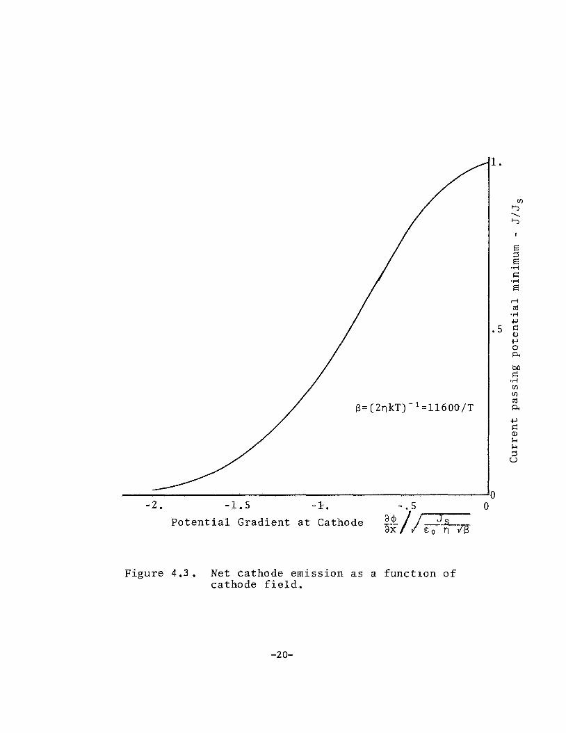
Figure 4 . 3 shows t h e r e l a t i o n between t h e f r a c t i o n of s a tu ra t ion cur ren t escaping t h e p o t e n t i a l minimum i n a nonmagnetic diode and t h e p o t e n t i a l g rad ien t a t t h e cathode surface. ab ly w e l l approximated by a l i n e a r function.
The r e l a t i o n can be reason- It is then considered t o
-17-

I
Figure 4.1. Construction for Trajectory Calculation.
-18-

E c c, .f-i k
M 30
u
3 a, 2: . *e. - - -
-0. - - *
- -
, --
I
w E E-. H
lp
iJ
B
-19-
- 2 . - 1 . 5 - E . - . 5 0 P o t e n t i a l Grad ien t a t Cathode ?$./IF
ax O I I J C S '
F igu re 4 . 3 . Net ca thode emiss ion as a f u n c t i o n o f ca thode f i e l d .
-20-

apply i n t h e present case (s ince v e l o c i t i e s are so s m a l l as t o r e s u l t in no appreciable Lorentz force) t o determine t h e ne t cur ren t passing the p o t e n t i a l minimum. Actually, s ince the computer does not simulate t h e charge between cathode and po ten t i a l minimum, the cathode gradient is modified by t h e amount of missing charge.
4.2.6 Beam In j ec t ion
The in jec ted beam is represented by a set of NK charge elements-- as few as 5, as many as 10 or 20--equally spaced on the same in j ec t ion circle. stream is thus monoenergetic, t h e stream resu l t ing from space-charge forces a f t e r a few time s t eps nevertheless has a f i n i t e width and energy spread. but t h i s has not ye t been done. MARGE, l i s t e d i n Appendix A.9. ted e lec t ron i n t o t h e t o t a l charge array, "cleans out" in jec ted pa r t i - cles a f t e r t h e i r t r a n s i t through t h e in t e rac t ion space, and p r i n t s ou t r e s u l t s of t he t i m e s tep. t h e space-charge fo rce evaluation routine.
They a l l have the same in j ec t ion veloci ty . While the in jec ted
It would be des i rab le t o i n j e c t a stream with ve loc i ty spread, This process i s done.in the subroutine
MARGE a l so merges the in jec ted o r e m i t -
It then advances t i m e and r e tu rns cont ro l t o
4.2.7 Waveform Analysis
A t i n t e r v a l s i n the simulation, a Fourier ana lys i s i s performed on The r e s u l t s are a l l e lectrode po ten t i a l s and induced charge waveforms.
of i n t e r e s t i n themselves and a l so as an ind ica t ion of steady state. Jk, fundamental, second and t h i r d harmonics are calculated.
The analys is is a r a the r simple-minded one i n which the waveforms are mult ipl ied by trigonometric functions and integrated using Simpson's ru le . The in tegra t ions are extended over t h e r f cycle j u s t completed, however, s ince it would obviously be incorrect t o include the t r ans i en t . The one-cycle in tegra t ion range a l so gives a good indica t ion of depar- t u r e ( f luctuat ion) from steady state.
4.2.8 Graphic Output
Miscellaneous programs are a l so l i s t e d i n Appendix A. They serve var ious housekeeping chores and are of no spec ia l i n t e r e s t s c i e n t i f i c a l l y ; the l i s t i n g is f o r t h e sake of completeness.
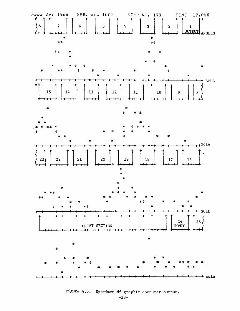
The graphic output program deserves spec ia l mention, however, because of its value i n providing a quick check on the operation of t he program and f o r valuable in s igh t i n t o t h e in t e rac t ion i t s e l f . d i sp lay of t h e Amplitron's e lec t ronic ensemble is shown i n Figure 4.4; that f o r t he in jec ted beam amplif ier , i ac t ion space of t h e in jec ted beam de*c p l o t is impractical . rants, each of which is p lo t ted i n Cartesian r-€I coordinates.
A specimen of t h e
Figure 4.5. The annular i n t e r - gdcso slender that t h e polar
The annulus is therefore s p l i t i n t o i t s four quad-
These p l o t s can be of even g rea t e r use i f viewed sequentially, as i n a motion p ic ture .
-21-

- 7246 I S r C P hrc. l e i
* * *
* * f f *
* . * * * .
* e .. . -22-
* **
DRIFT SECTION INPUT
t **
*
Figure 4 .5 . Specimen df graphic computer output. -23-
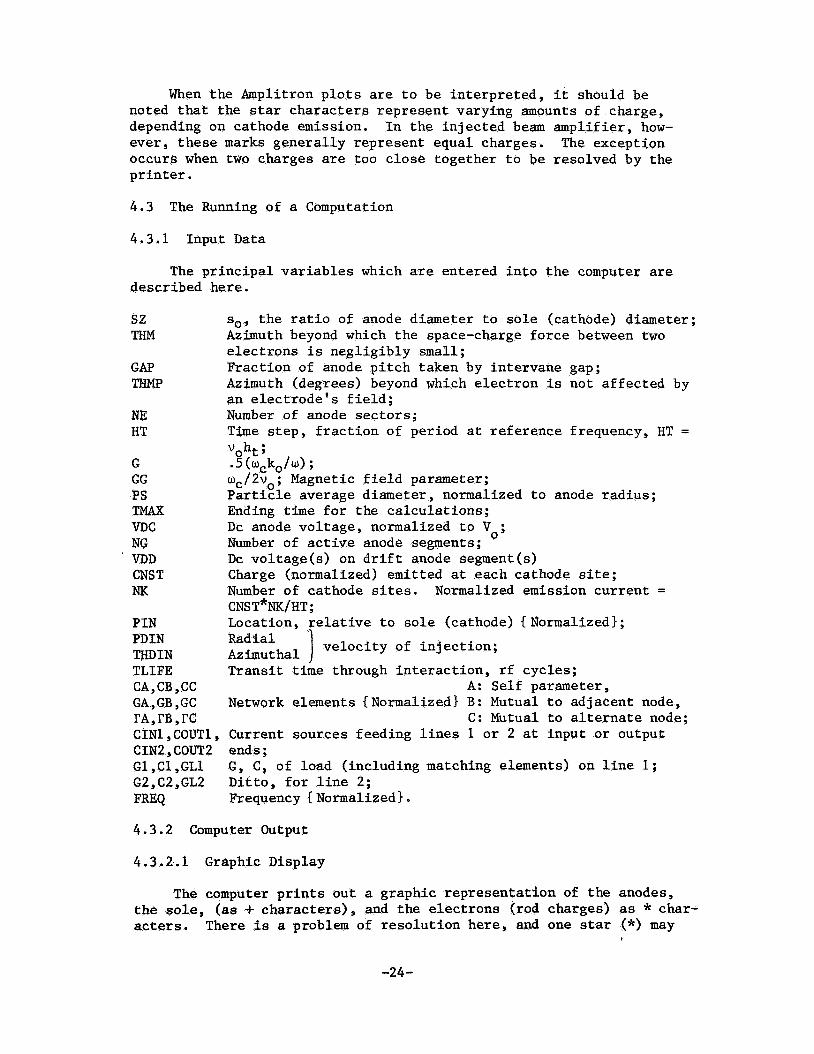
When t h e Amplitron p l o t s are t o be in t e rp re t ed , i t should be noted t h a t t h e star charac te rs represent varying amounts of charge, depending on cathode emission. I n t h e in j ec t ed beam ampl i f ie r , how- ever, these marks genera l ly represent equal charges. The exception occurs when two charges are too c lose together t o be resolved by the p r i n t e r .
4.3
4.3.1 Input Data
The Running of a Computation
The p r inc ipa l va r i ab le s which are entered i n t o t h e computer are described here.
SZ m
GAP THMP
NE HT
G GG PS TMAX VDC NG VDD CNS T NK
PIN PDIN THDIN TLIFE CA, CB ,CC GA,GB,GC TA, I'B , I'C C I N l , C O U T l , CIN2,COUT2 G 1 , C 1 ,GL1 G2,C2,GL2 FREQ
s o , t h e r a t i o of anode diameter t o so l e (cathode) diameter; Azimuth beyond which t h e space-charge fo rce between two e l ec t rons is negl ig ib ly small; Fraction of anode p i t c h taken by intervane gap; Azimuth (degrees) beyond which e l ec t ron i s not a f fec ted by an e l ec t rode ' s f i e l d ; Number of anode sec to r s ; T ime s t e p , f r a c t i o n of period a t re ference frequency, HT = voht ; -5 (ocko/w) ; wc/2v0; Magnetic P a r t i c l e average
f i e l d parameter; diameter, normalized t o anode rad ius ;
Ending time f o r the ca lcu la t ions ; D c anode vol tage , normalized t o Vo; Number of active anode segments; D c vo l tage(s ) on d r i f t anode segment(s) Charge (normalized) emitted a t each cathode site; Number of cathode sites. Normalized emission cur ren t =
Location, r e l a t i v e t o s o l e (cathode) {Normalized); CNST*NK/HT ;
ve loc i ty of i n j ec t ion ; I Ftadial Azimuthal Trans i t time through in t e rac t ion , r f cycles;
Network elements {Normalized) B: Mutual t o adjacent node,
Current sources feeding l i n e s 1 o r 2 at input o r output ends; G, C, of load (including matching elements) on l i n e 1; Di t to , f o r l i n e 2; Frequency { Normalized 1 .
A: Self parameter,
C: Mutual t o a l t e r n a t e node;
4.3.2 Computer Output
4.3.2.1 Graphic Display
The computer p r i n t s out a graphic representa t ion of the anodes,
There i s a problem of r e so lu t ion here, and one star (*) may t h e so l e , ( a s + charac te rs ) , and the e l ec t rons (rod charges) as * char- acters.
-24-
represent more than one e lec t ron . a l l stars represent t h e same amount of charge; i n the inject device, they genera l ly do. The graphic d isp lay comes at con i n t e r v a l s , but comes once each s t e p within t h e last 2 cycles of the end.
I n the Amplitron ca lcu la t ions , not
4 . 3 . 2 . 2 Anode Electrode Data
Each time s t e p the computer p r i n t s out t h e following d a t a f o r each anode electrode:
Number; RF I n s t . po ten t i a l ; induced charge; induced cur ren t ( the d i f f e rence from t h e previous induced charge); amount of charge co l lec ted ; energy of bombardment. The t o t a l induced charge, t o t a l anode co l l ec t ion cu r ren t and t o t a l anode bombardment energy are pr in ted on another l i ne . Similarly, t he po ten t i a l , c o l l e c t i o n charge and bombardment energy f o r t h e s o l e are pr in ted . The i n j e c t i o n charge and current are a l s o printed.
I f p a r t i c l e s are removed from the i n t e r a c t i o n on account of having passed through it a x i a l l y , t h e co l l ec to r statistics are printed: amount of each charge element, its radial loca t ion , ve loc i ty components and k i n e t i c energy. a l s o punched f o r use i n poss ib le f u r t h e r computations.
Within the last cycle of a computer run, these da t a are
The computer a l s o p r i n t s out t h e value of t h e au tocorre la t ion func- t i o n
ACF = 1 Q(t) Q(t-T)
computed f o r t h e previous r f cycle, where Q is t h e induced charge a t the e lec t rode #l. This quant i ty is un i ty f o r a steady-state, and is used to . determine whether t h a t condition has ar r ived .
4 . 3 . 2 . 3 Further Manipulation and In t e rp re t a t ion of t h e Computer Output
It is f i r s t of a l l a good idea t o p l o t t h e v a r i a t i o n with time of some such key quant i ty as t h e Fourier amplitude of t h e output voltage. This genera l ly shows slow v a r i a t i o n f o r t h e f i r s t few r f cycles a f t e r a parameter is changed. space of a few cyc les e x h i b i t s a wild o s c i l l a t o r y t r ans i en t o s c i l l a t i o n . After a t o t a l of about 2k0 cycles the o s c i l l a t o r y t r a n s i e n t begins t o disappear, and the Fourier amplitude approaches some steady state. There is usua l ly some f l u c t u a t i o n about t h i s level, however, and it may be so severe as t o obscure t h e steady level o r render i t impossible t o determine accurately.
It then begins t o vary r ap id ly and over t h e
In those cases where steady state f a i l e d t o appear with reasonable In some ce r t a in ty , considerable study w a s made t o determine t h e cause.
cases t h e r o o t w a s no t found, but a de ta i l ed Fourier ana lys i s covering many cycles d isc losed a reasonably p rec i se value f o r t he s p e c t r a l com-
s i g n a l frequency. This but one of many poss ib le pproaches t o t h e use of t computer output. Another is
-25-
simply t o take t h e average value of t he Fourier fundamental amplitude as determined by examining the p lo t . t o be avoided, however.
The use of such averaging methods i s
Further ana lys i s of the computer output cons i s t s i n summing the c o l l e c t i o n of charge and bombardment energ ies f o r the var ious e lec t rodes over t he space of one cycle a f t e r steady state is a t t a ined . y i e ld the convection cu r ren t s and bombardment powers associated with t h e several anodes, t h e anode as a whole, the s o l e and the co l l ec to r . I n the case of t he c o l l e c t o r , i t is assumed t h a t e l ec t rons are in te rcepted a t the r a d i a l l oca t ions a t which they emerge from the i n t e r a c t i o n region, without f u r t h e r acce le ra t ion o r dece lera t ion . This might be accomplished, f o r example, by use of a c o l l e c t o r having i n f i n i t e l y many segments, each at the dc p o t e n t i a l corresponding t o i t s r ad ius .
These f i g u r e s
The d c input power t o t h e device is thus given by t h e sums of t he
The use fu l ly generated r f power i s the d i f f e rence between the
anode dc input power, VbIb, and the co l l ec to r dc input power, i n VcQc o r
< V c > I c .
output power, V:G1/2, and the input power, Coutl 2/2G,.
mental frequency values. t h i s u se fu l ly generated power t o the dc input power. e s t ab l i sh ing an energy balance, account must a l s o be made of harmonic power (negl ig ib le here) and the fundamental power transmitted t o the input source by v i r t u e of t h e so-called "hot mismatch." The la t ter is a l s o neg l ig ib l e i n these devices.
These are funda-
For the purposes of The e f f i c i ency is calculated as the r a t i o of
5. Amplitron Calculations
5.1 Parameters
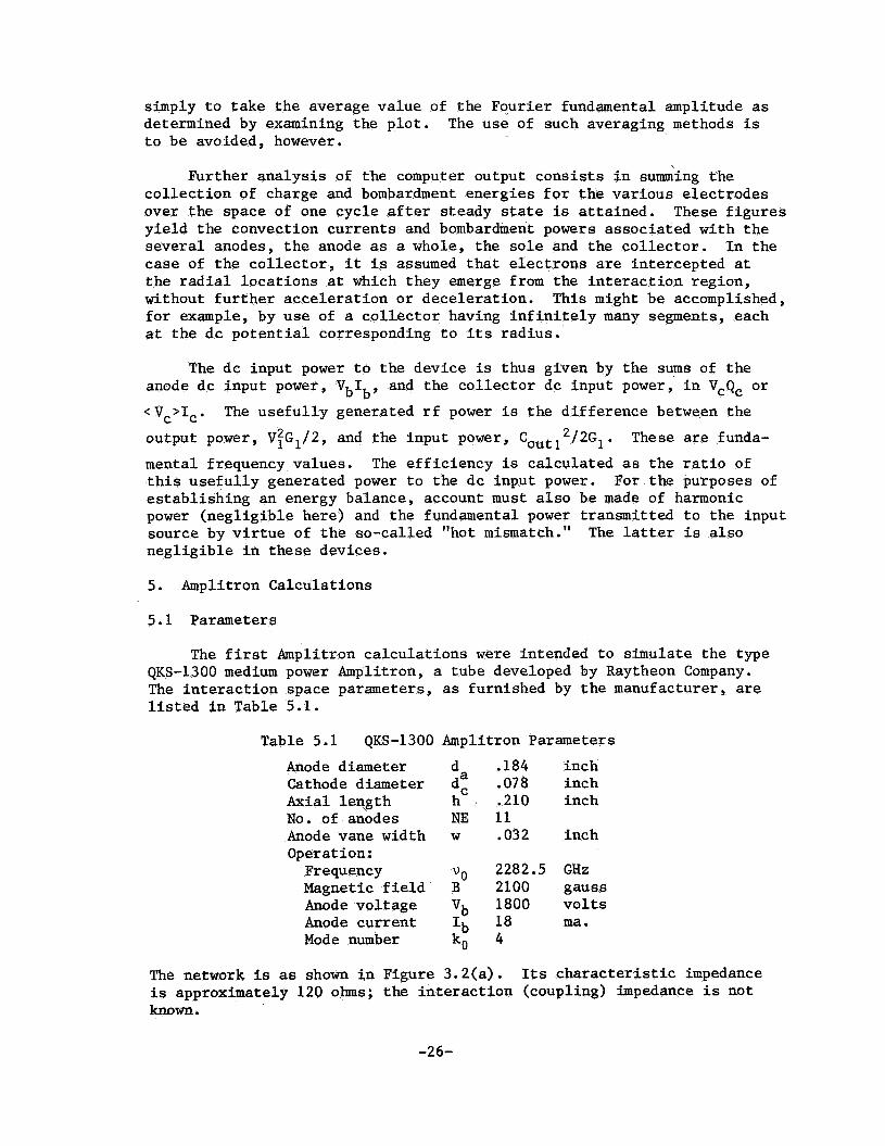
The f i r s t Amplitron ca l cu la t ions were intended t o simulate t h e type QKS-1300 medium power Amplitron, a tube developed by Raytheon Company. The i n t e r a c t i o n space parameters, as furnished by t h e manufacturer, are l i s t e d i n Table 5.1.
Table 5.1 QKS-1300 Amplitron Parameters
da Anode diameter Cathode diameter Axial length No. of anodes NE Anode vane width w Operation :
3
Frequency vO Magnetic f i e l d B Anode vol tage vb Anode cur ren t Ib Mode number k0
.184 inch
.078 inch
.210 inch 11 .032 inch
2282.5 GHz 2100 gauss 1800 v o l t s 18 m a . 4
The network is as shown i n Figure 3.2(a). i s approximately 120 ohms; t he i n t e r a c t i o n (coupling) impedance i s not known.
Its c h a r a c t e r i s t i c impedance
-26-

Preliminary ca l cu la t ions w e r e made with computer network parameters from previous Amplitron research which provide t h e proper phase constant, v i z . 49.0909 ... degrees per cell . network, however, w a s high (1480 ohms), and the r f input power level w a s a l s o high (3.17 Po). with which t o start t h e computations quickly; they can be relaxed once a large-signal configuration is obtained.
The c h a r a c t e r i s t i c impedance of t h i s
These exaggerations provide f o r strong r f f i e l d s
5.2 Results
The ca l cu la t ions were run i n i t i a l l y with a time s t e p of .1 cycle. After reaching steady state the time i n t e r v a l w a s reduced t o .05 cycle and f u r t h e r ca l cu la t ions were made f o r refinement. f i g u r a t i o n i s shown i n Figure 4.4. forms were used t o compute t o t a l r f output power from t h e simple average of V2(T)G.
The space-charge con- The computed output vo l tage wave-
The r e s u l t s are shown i n Table 5.2.
Table 5.2 Results of Amplitron Calculations Nos. 7/19/67 & 7/24/67
T i m e i n t e r v a l .1 .05 Anode cur ren t , I b 210 337 m a . D c input power 310 500 w a t t s Rf output power 291 450 w a t t s Gain 8.3 10.2 db Efficiency 86. 83. percent.
The dc anode cu r ren t s are g rea t e r than i n t h e a c t u a l Amplitron by an order of magnitude; t h e r f output powers are correspondingly high. This is the r e s u l t of computation with high impedance and high r f input power. This magnitude of impedance probably cannot be rea l ized i n a real tube, nor could the cathode emission be obtained.
It w a s noted t h a t t he energy balance i n t h i s ca l cu la t ion w a s poor; t h e t o t a l dc and r f input power does not account quan t i t a t ive ly f o r t he t o t a l r f output power and the anode bombardment rate. This i s a t least i n p a r t caused by e r r o r s i n the t r a j e c t o r y ca lcu la t ions , which are aggravated by t h e smallness of the cathode and by the r e l a t i v e l y high cyclotron frequency.
5.3 Termination of Amplitron Computations
Shor t ly a f t e r t he preliminary ca l cu la t ions reported above, no t i ce w a s received t h a t t h e Amplitron w a s no longer of i n t e r e s t f o r t h e particu- lar app l i ca t ion requiring i t s numerical ana lys i s . pu ta t ions were therefore terminated and a l a y s i s of t he in jec ted beam forward-wave ampl i f ie r commenced.
The Ampfitron com-
6 . In jec ted Beam Forward-Wave Amplifier Calculations
The ca l cu la t ions made f o r t h e in jec ted beam forward wave amplifier had t h e immediate objec t ive of providing information relative t o a
-27-
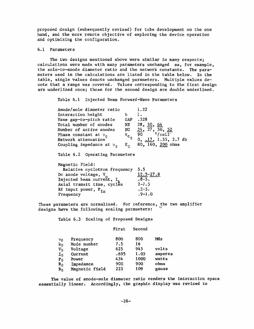
proposed design (subsequently revised) f o r tube development on t h e one hand, and the more remote objec t ive of exploring t h e device operation and optimizing t h e configuration.
6.1 Parameters
The two designs mentioned above w e r e s i m i l a r i n many respec ts ; ca l cu la t ions were made with many parameters unchanged as, f o r example, t h e sole-to-anode diameter r a t i o and t h e network constants. The para- meters used i n the ca l cu la t ions are l i s t e d i n t h e t a b l e below. I n the t ab le , s i n g l e values denote unchanged parameters. Multiple va lues de- no te t h a t a range w a s covered. are underlined once; those f o r t he second design are double underlined.
Values corresponding t o t h e f i r s t design
Table 6.1 In jec ted Beam Forward-Wave Parameters
Anode/sole diameter r a t i o 1.22 In t e rac t ion height h 1. Vane gap-to-pitch r a t i o GAP .328 Tota l number of anodes NE 28, 30, Number of active anodes NG 24, 27, 30, 52 - Phase constant a t v o 0, 90 O / ceW Network a t tenuat ion 0, 2, 1.35, 2.7 db Coupling impedance a t v o KO 8 0 , 1 6 0 , 3 ohms
Table 6.2 Operating Parameters
Magnetic Field:
D c anode vol tage , In jec ted beam curren t , Axial t r a n s i t time, cycles
Relative cyclotron frequency 5.5 12.5-27.8 8-5.
2-7.5 Rf input power, Pin -2-5.
-- vO
Frequency .9-1.0
'k
These parameters are normalized. For reference, the two amplifier designs have t h e following sca l ing parameters: b
Table 6.3 Scaling of Proposed Designs
F i r s t Second
vo Frequency 800 800 MI2
VO Voltage 625 945 v o l t s
RO Impedance 900 900 ohms
ko Mode number 7.5 16
IO Current .695 1.05 amperes PO Power 434 1000 w a t t s
BO Magnetic f i e l d 233 109 gauss
The value of anode-sole diameter r a t i o renders the in t e rac t ion space e s s e n t i a l l y l i n e a r . Accordingly, t he graphic d i sp l ay w a s revised t o
-28-
provide b e t t e r reso lu t ion ; t y p i c a l output is shown i n Figure 4.5.
This magnetic f i e l d is high f o r t h e frequency involved, i .e . , t he cyclotron frequency i s high r e l a t i v e t o t h e s igna l frequency. Fortu- na te ly , t h e t r a j e c t o r y computation d i f f i c u l t y i t poses had been solved as described i n Section 4.2.4.
The number of anode segments and wavelengths i s much l a rge r f o r t h i s ampl i f ie r than fo r t he Amplitron ca l cu la t ions f o r which the program w a s o r i g i n a l l y developed. cause of t h e g rea t e r number of e lec t rodes and a l s o because t h e simulation requi res a niminum number of e l ec t rons p e r wavelength, and the re are more of these . Fortunately, t h e new computer has adequate capacity. The execution t i m e is a l s o a f fec ted , however, and t h i s is more se r ious than s torage problems. The time required f o r each t i m e i n t e r v a l increases as t h e square of t h e mode number, ko, because more e l ec t rons are involved. I n addi t ion , more r f t i m e is required f o r t h e e n t i r e ca lcu la t ion ; t h i s i s proportional t o t h e mode number. proportional t o t h e cube of t h e mode number. t h e new computer (IBM 360/65) i s much f a s t e r than the o lder one (IBM 7040) and has a more powerful c e n t r a l processor which a f fo rds a fu r the r increase i n speed.
Computer s torage requirements are increased be-
The execution t i m e thus i s roughly Again, i t i s fo r tuna te t h a t
6.2 Results
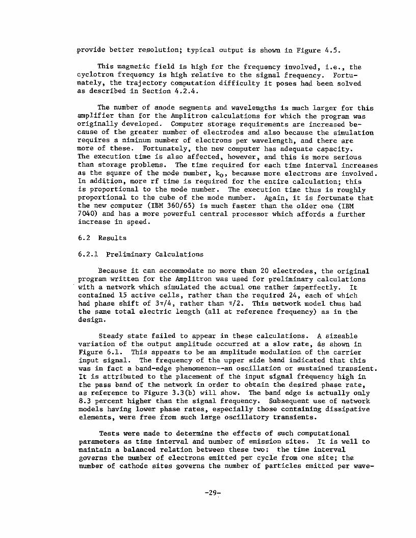
6.2.1 Preliminary Calculations
Because i t can accommodate no more than 20 e lec t rodes , t h e o r ig ina l program wr i t t en f o r t he Amplitron w a s used f o r preliminary ca l cu la t ions with a network which simulated the a c t u a l one r a t h e r imperfectly. It contained 15 active cells, r a the r than the required 24, each of which had phase s h i f t of 31~/4 , r a the r than .rr/2. t h e same t o t a l electric length ( a l l a t reference frequency) as i n t h e design.
This network model t hus had
Steady state f a i l e d t o appear i n these ca lcu la t ions . A s izeable v a r i a t i o n of t h e output amplitude occurred a t a slow rate, As shown i n Figure 6.1. This appears t o be an amplitude modulation of t h e carrier input s igna l . The frequency of t h e upper s i d e band indicated t h a t t h i s w a s i n f a c t a band-edge phenomenon--an o s c i l l a t i o n o r sustained t r ans i en t . It i s a t t r i b u t e d t o t h e placement of t h e input s igna l frequency high i n t h e pass band of t h e network i n order t o obta in the desired phase rate, as reference t o Figure 3.3(b) w i l l show. The band edge i s ac tua l ly only 8.3 percent higher than t h e s igna l frequency. Subsequent u se of network models having lower phase rates, e spec ia l ly those containing d i s s i p a t i v e elements, were f r e e from such l a r g e o s c i l l a t o r y t r ans i en t s .
T e s t s w e r e made t o determine t h e e f f e c t s of such computational parameters as time i n t e r v a l and number of emission sites. maintain a balanced r e l a t i o n between these two: t h e t i m e i n t e r v a l governs t h e number of e l ec t rons emitted p e r cycle from one site; t h e number of cathode sites governs t h e number of p a r t i c l e s emitted per wave-
It is w e l l t o
-29-
3
E c a a, a 1 c, .rl d
2 a 4 a c, G 2 a, E a a G 1 c4
Q 1 p1 c, 3 0 '
c4
k 0
n cn a k a cl I z
a , l
v
cn a, M k a c: U
rcl 0 ..
0
/ /
I I I
30 4 0 50 TIME, T - RF CYCLES
Figure 6 . 1 . Extension of CFA calculation #010268: Failure to Reach Steady State
-3 0-
l ength a t each time. Together, they con t ro l t h e t o t a l number of elect- t rons . It w a s genera l ly found t h a t a time i n t e r v a l of .1 cycle and one emission s i t e per wavelength descr ibe t h e stream f a i r l y w e l l . p rec is ion would on occasion be needed; i t would be more expensive.
Better
6.2.2 Demodulation & Feedback Through t h e Stream
It became apparent i n t h e preliminary s tage t h a t considerable r f cur ren t w a s being induced i n t h e anode segments of t h e d r i f t region. When t h i s stream reaches t h e input region of t h e r f delay l i n e , t he re i s a strong s i g n a l fed back i n t o t h e e l ec t ron stream-network system, a f f e c t i n g t h e performance of t h e ampl i f ie r .
Information r e l a t i v e t o t h e a c t u a l device w a s lacking a t t h e time, hence preliminary computer experiments w e r e made with schemes f o r art i- f i c i a l l y removing t h e stream modulation i n t h e stream as it passes through t h e d r i f t region. This cons i s t s i n replacing reenter ing e l ec t rons with newly-injected ones i n the d r i f t region. Although a r t i f i c i a l i n t he sense t h a t t h e energy balance i s destroyed f o r those e lec t rons , computations were made which showed t h a t t h e r f stream feedback w a s indeed reduced. It w a s not eliminated completely, however, because although t h e ve loc i ty modulation and the r a d i a l displacement modulation were eliminated, the azimuthal modulation w a s not. This i s inev i t ab ly t i e d i n wi th t h e f a c t t h a t an e l ec t ron is present a t some azimuthal pos i t ion and t h e computer has no information as t o where it would have been had the re been no r f s igna l . t h e f a c t t h a t some e lec t rons reentered and some did not (because of t h e i r r f i n t e r a c t i o n i n "favorable phase") would fu rn i sh a dens i ty modulation of t h e reenter ing stream.
Even i f i t d id , and the e l ec t ron were moved t o such a loca t ion ,
Details of t h e a c t u a l device demodulation system w e r e f i n a l l y ob- tained. This c o n s i s t s of a v a r i a t i o n with azimuth of t h e dc electric f i e l d i n t h e d r i f t region. r ead i ly by assignment of d i f f e r e n t dc vol tages t o t h e several segments of t h e d r i f t por t ion of t h e anode. model, which represents a phys ica l ly r e a l i z a b l e scheme, have a v a l i d i t y concerning energy balance and e f f i c i ency t h a t t h e o thers do not . c o l l e c t o r statistics, i.e., t h e information as t o where e l ec t rons are t o be co l lec ted and at w h a t bombardment energied, are no longer subject t o t h e e r r o r s of t h e a r t i f i c i a l scheme. The r e s u l t s s t i l l showed, however, t h a t t h e rf stream curren t p e r s i s t s , although it i s reduced t o about t h e same degree as observed i n t h e a r t i f i c i a l scheme, v i z . , a reduction of about 15 db i n current-squared.
It is simulated i n t h e computer r a t h e r
Computations made with t h i s computer
The
6.2.3 I n s t a b i l i t i e s at High Gain
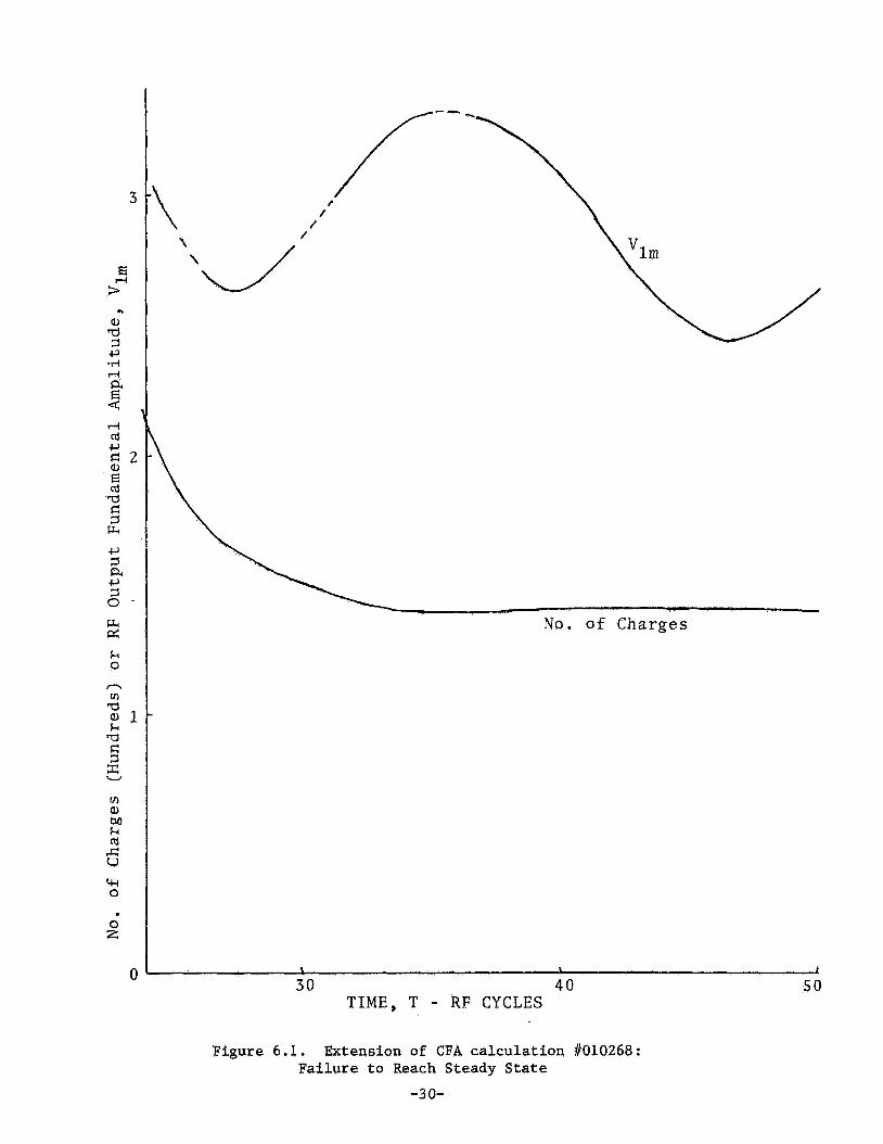
The previous, preliminary ca l cu la t ions had been made with r e l a t i v e l y high r f input power and therefore resu l ted i n low ga in (c. 6-10 db). The course of t h e ca l cu la t ion program w a s thus t o reduce t h e input power t o a t t a i n t h e ga in level of approximately 20 db reported f o r experimental tubes. reach steady state w e r e noted. Consid- e r a b l e e f f o r t w a s made t o determine i t s cause and t o eliminate it; t h i s
As t h i s w a s being done, f u r t h e r f a i l u r e of t he ca l cu la t ions t o Figure 6.2 shows such behavior.
-31-
, ./
b I . In e M
ccr 0
a, 4 F4
x w 2
-3 2-

has not been completely successful.
The apparent a-m of t h e output s igna l does not appear i n t h i s case t o be r e l a t e d t o t h e band-edge.
It w a s thought a t f i r s t t h a t a computational i n s t a b i l i t y might be The time i n t e r v a l , HT, and t h e number of emission poin ts , NK,
Halving HT o r doubling NK r e s u l t s i n doubling t h e number
Indeed, t h e v a r i a t i o n s i n output w e r e
Moreover, halving t h e time s t e p has t h e add i t iona l e f f e c t
It w a s concluded t h a t t h e computer program w a s not
involved. w e r e varied. of e l ec t rons i n the problem. a b l e e f f e c t on t h e i n s t a b i l i t y . remarkably a l i k e , i nd ic a t i n g t h a t t h e stream w a s w e l l represented t o begin with. of improving t h e accuracy of t he t r a j e c t o r y ca l cu la t ions and a l s o of t he network ca lcu la t ions . s e r ious ly involved.
This increase i n prec is ion had no notice-
On t h e p o s s i b i l i t y t h a t t h e apparent i n s t a b i l i t y might be a mani- f e s t a t i o n of some kind of plasma or cyclotron wave i n s t a b i l i t y , calcu- l a t i o n s were made without computing space-charge forces . t h e same degree of f l u c t u a t i o n as those with space-charge taken i n t o account. Neglect of space-charge forces , inc identa l ly , appears as a d i s t o r t i o n of t h e spoke configuration, as shown i n Figure 6 . 3 .
This showed
The ca l cu la t ions w e r e a l s o run with increased de anode voltage. Such a parameter change would alter t h e degree of traveling-wave i n t e r - ac t ion and hence change t h e na ture of any i n s t a b i l i t y r e l a t e d t o t h e p r inc ipa l mode of i n t e rac t ion . ab le change w a s seen with a 5% increase i n dc anode vol tage as compared with t h e o r i g i n a l dc anode vol tage , which w a s t h e Hartree voltage.
I n t h i s computer experiment, no appreci-
The o s c i l l a t i o n s w e r e observed both with and wi thou t , t he de vol tage taper i n t h e d r i f t sec t ion .
The network w a s i n one computer experiment de l ibe ra t e ly mismatched wi th a resistive load having a r e f l e c t i o n c o e f f i c i e n t of 1/3. at both ends. at t h e wavelength d i c t a t e d by t h e network c h a r a c t e r i s t i c , and the input s igna l l e v e l i s g r e a t l y increased by the presence of i n t e r n a l network feed- back, while t h e output level remains much t h e same. network mismatch i s not r e l a t e d t,o t h e ~ i r l s t a b i l i t y of concern here.
As seen i n Figure 6 . 4 , a standing-wave pattern appears i n t e r n a l l y
It i s concluded t h a t
Calculations w e r e i n one case run f o r a much longer period than previously, with t h e r e s u l t shown i n Figure 6.5. presence of a s i g n a l a t about 30% higher and lower frequencies relative t o t h e s igna l . Fourier ana lys i s of t he waveform obtained from t h e com- puter resu l ted i n t h e spectrum shown i n Figure 6.6. t h e ex is tence of a component at 1 . 3 vo, which is of t h e same order of magnitude as t h e second harmonic. however, t o t h i s frequency i n terms of network proper t ies . (The band edge is at 42 uo.)
The v a r i a t i o n suggests
This indeed v e r i f i e s
There is no p a r t i c u l a r s ign i f icance ,
From a l l t h e above evidence, i t began t o appear that t h e long period (c. 16 cycles) of t h e rapid o s c i l l a t i o n s w a s r e l a t e d t o t h e s igna l t r a n s i t
-33-

-34-
JUNE 26, 1968 sm. NO. 6012 STEP NO. 150 TIME 15.000
+ + + + ++ + $ $ + + $ = : $ $ $ + + ++ I+*p t++++S $++++$ b+*$ +++++I- $++++-I-$ * * ** ** *
S i $ + f + Y
44 * * *-** * *" 96 * * * * * *
!t * * * * * * * * * * *
ii Ir_l + + + + + + + + + + + + + + + + + + + + + + + +
+ + + + + + + + + ++++++++-i-t++++ ++++++ *++*$$ ++++++ +++I++ +++I-+++
* 'Mc ** * * w* * * *
* 3tJt. * * w * * * * * M * * * * * ** * M - : : : : : : : ! : : : : : : : : ; * : : : : : ::::::CH-w-H
* *H$* * * *
+ + + + - + + + + + + + +++++ ++-I-+++ +++++++ : $ $ $ + + + + + +
$ + L-+$ $+++A L+++ $++++S +++++I-
* *** * * * * * ***M** * * * * * * * * * *
** Jwc ** * * * * *
+ + +I- t t f. + + + ...................................... +++++++ +++
** * * H* w x3t)c* ** * * * Jc;x- * *-Jc-w. ** , I t
Figure 6.3 Calculat ion 6.12; Space-chwge forces omitted; A r t i f i c i a l stream demodulation.
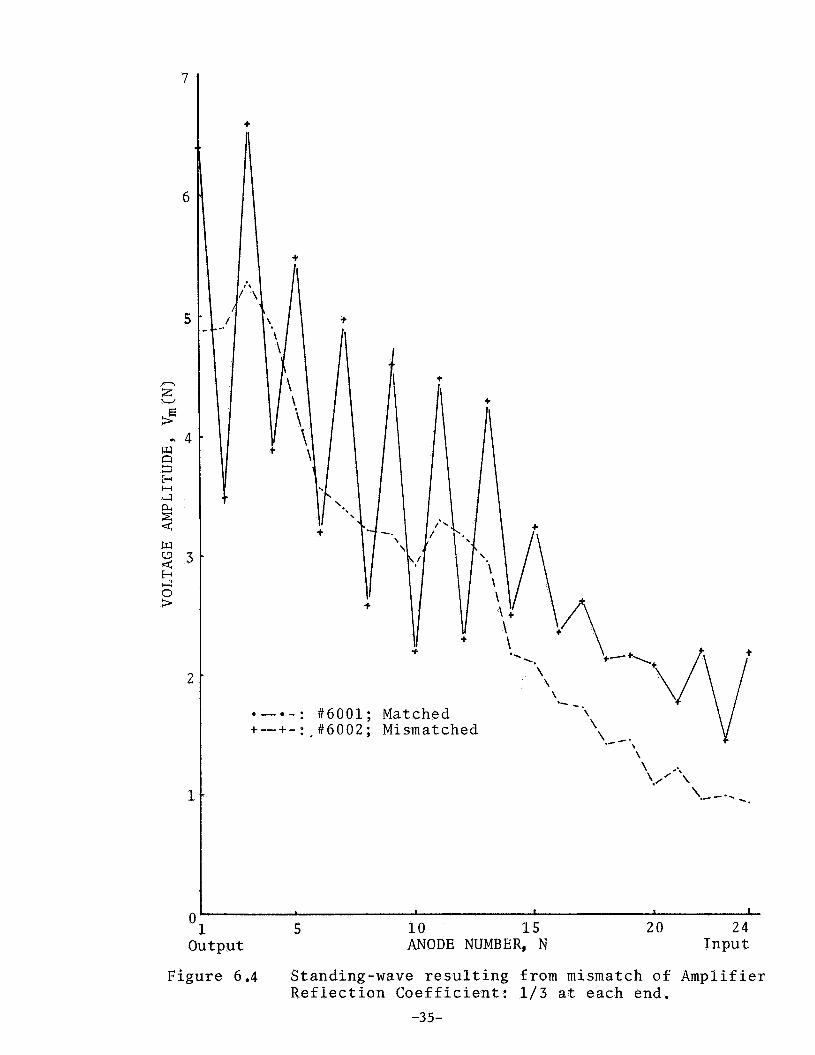
I I t I
5 10 15 20 24 output ANODE NUMBER, N Input O L 1
Figure 6.4 Standing-wave resulting from mismatch of Amplifier Reflection Coefficient: 1/3 at each end.
-35-
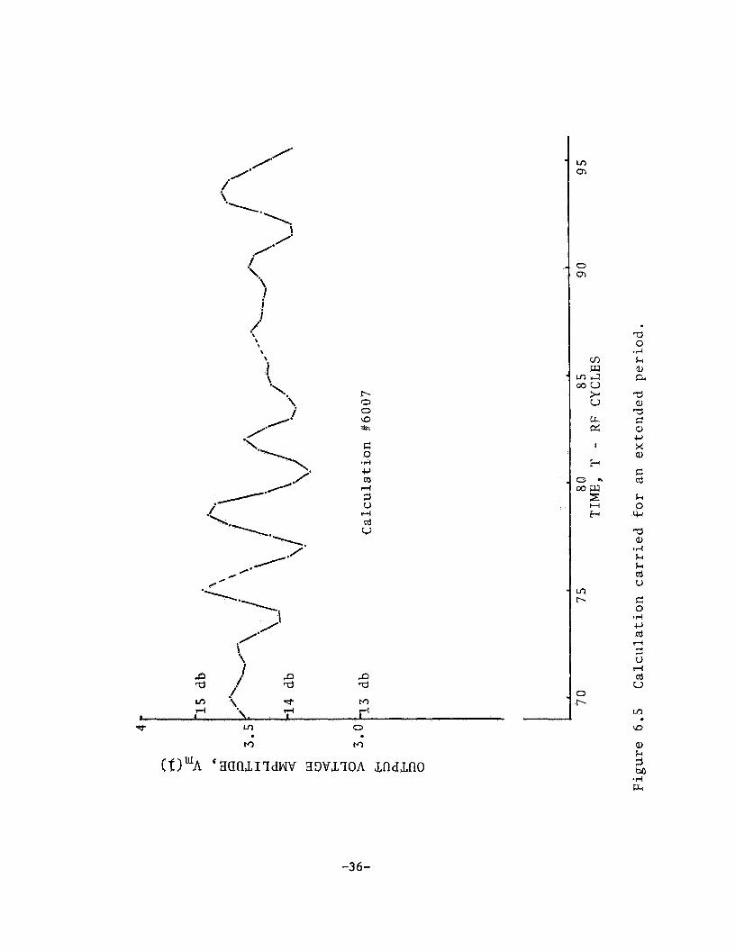
Fc 0 3 0 *
Ln 0
M .
M
83VLL1OA
-36-
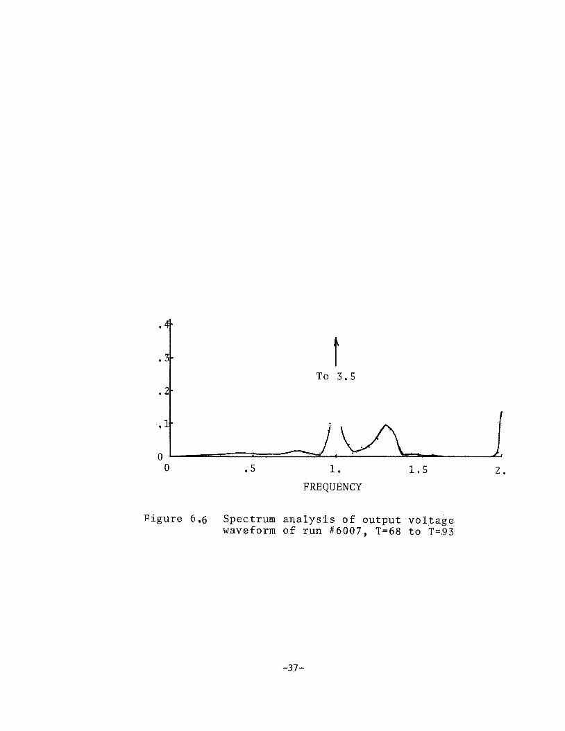
* 4 -
b 3-
-ro 3 . 5
. I- I
J, 0 * 5 1. 1.5 2 .
FREQUENCY
Figure 6.6 Spectrum analysis of output voltage waveform of run # 6 0 0 7 , T=68 to T=93
-37-
time through t h e network (6 cycles) o r t o t h e t o t a l t i m e required f o r synchronous e l ec t rons t o circumnavigate t h e cathode (7.5 cyc les when no d r i f t s ec t ion dc vol tage t ape r is involved, approximately 8 cycles when t h e vol tage v a r i a t i o n w a s used). The long period thus appears t o be about twice one of these t r a n s i t times. What appears t o be happen- ing is t h a t stream feedback allows a f luc tua t ion i n t h e output level t o pass through t o t h e input and excite a network t r a n s i e n t ; t h i s con- sists of a ringing o s c i l l a t i o n at band edge. causes it propagates along with t h e stream, tak ing 6 cycles t o pass fhrough t h e network and somewhat longer t o p a s s through t h e d r i f t sec- t i o n (attenuated) where i t then can re-excite a t r ans i en t . The f a c t that the r ing ing has a period of about two t r a n s i t s around t h e loop is perhaps r e l a t e d t o t h e phase of t h e feedback stream curren t .
The stream curren t t h a t
Figure 6.7 shows t h e t r a n s i t i o n from a ca l cu la t ion without a d r i f t vo l tage t ape r t o one i n which t h e dc vol tage abrupt ly drops t o 1 / 2 t he Hartree level as the e l ec t ron e n t e r s t h e d r i f t region, and then l i n e a r l y rises t o f u l l anode voltage. For t h e f i r s t 6 t o 8 cycles t h e o r i g i n a l output condifion p e r s i s t s , as t h e changed feedback conditions (mostly phase) cause a new s igna l t o be propagated from the input toward the output. Much t h e same s i t u a t i o n would appear i f the input s igna l had been changed r a t h e r than the d r i f t parameters. s igna l arrives at t h e output, t h e r e i s a rap id and l a r g e swing t o a lower level and, with rap id ringing, a slow, saw-tooth-like t r a n s i e n t t o a new steady state. ind ica t ive of t h e feedback pa th involved i n e l ec t ron reentrance. It appears, however, t h a t it takes much longer f o r t h e steady state (or semblance thereof) t o arrive than had previously been r ea l i zed .
After t h e new feedback
The period of t h i s saw-tooth i s 15 cycles,
As a t t e n t i o n w a s focused on stream feedback as t h e r o o t of t he
This has t h e f u r t h e r i n s t a b i l i t y , computer experiments w e r e run t o study the r o l e of t h e d r i f t reg ion and t h e phasing and a t t enua t ion i n it. ob jec t ive of studying t h e e f f e c t s of length of network and d r i f t spaces on the amplifier performance. t i o n 6.3, but t h e e f f e c t on the appearance of t r a n s i e n t o s c i l l a t i o n s w i l l be digcussed here. var ied i n s t e p s a t t h e expense of t h e length of d r i f t space; t h e r e s u l t s are shown i n Figure 6.8. case (NG24, NE=30) . After some r a t h e r v io l en t t r ans i en t s , t h e Fourier amplitude is seen t o settle down r a t h e r w e l l . d i f f e rence produced by changing t h e feedback p rope r t i e s of t h e d r i f t region relative t o t h e e n t i r e s igna l path. spec i fy t h e feedback more p rec i se ly because t h e phase s h i f t depends on e l ec t ron stream parameters, including t h e r f level.
More w i l l be sa id on t h i s subjec t i n Sec-
The length of t h e active sec t ion (NG) w a s f i r s t
The level at the start i s t h a t f o r t h e designed
This i s a t t r i b u t e d t o t h e
It is somewhat d i f f i c u l t t o
Additional evidence of t he r o l e of feedback is presented i n Figure 6 .9 , which p e r t a i n s t o a reduction i n the electrical length of t he circum- ference from 7.5 wavelengths t o 7.0. This allows comparison i n relative terms primarily. gain--probably because of t h e d i f f e r e n t feedback phase, but is a l s o less s tab le .
It shows t h a t t h e 7.0 wavelength system has higher
-38-

/ /
/ ,
P P a a
I *\
-39-
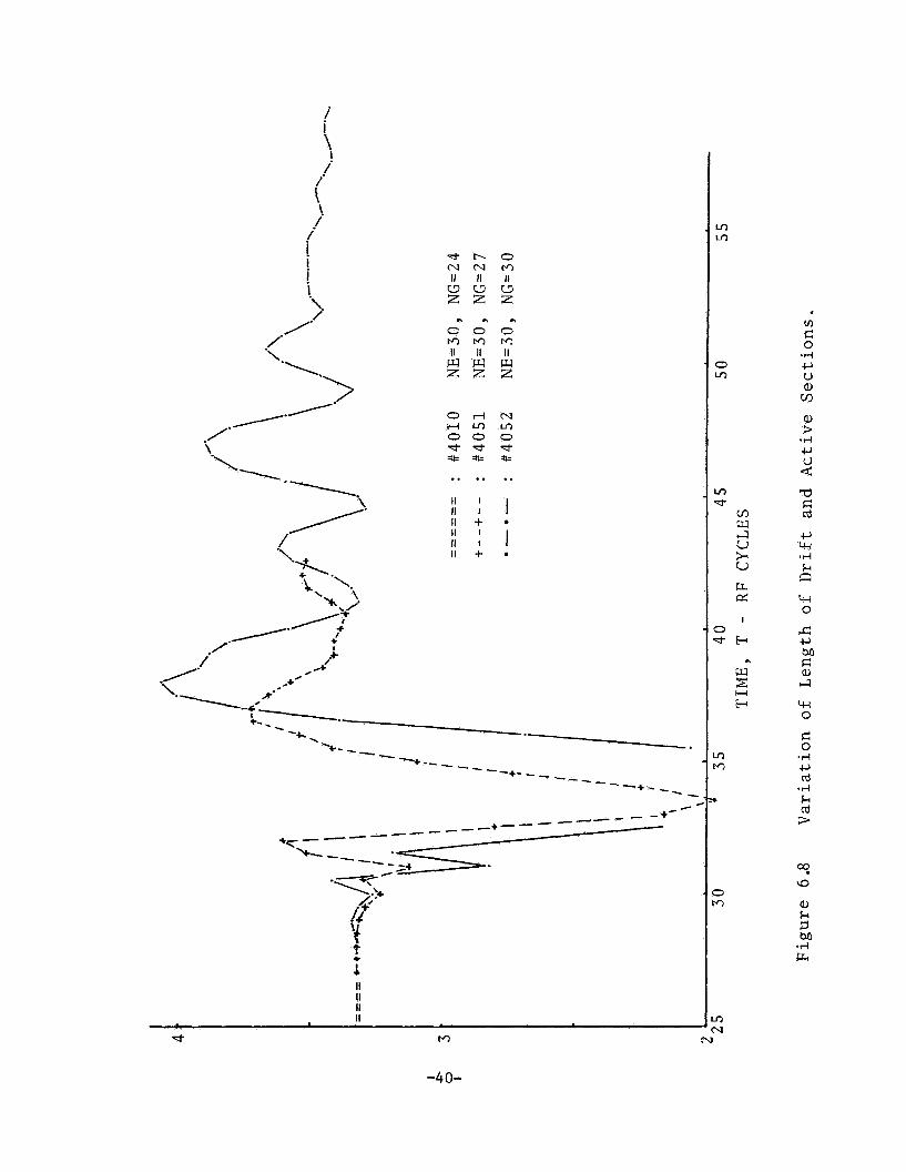
II I I I I w w w z z z
-40-
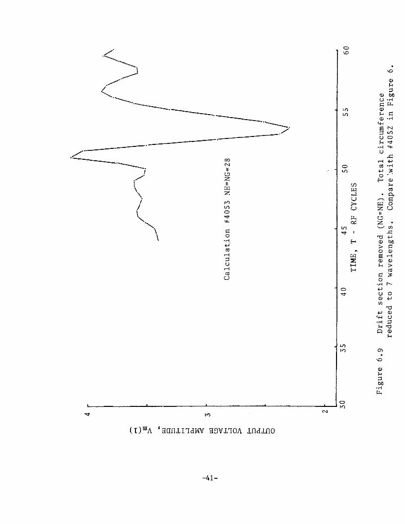
c) z II w z M In 0 d * F: 0 *r( c, cd d 1 u d cd U
N
-41-
Fina l ly , Figure 6.10 shows two ca l cu la t ions which d i f f e r i n tha t . by accident a p o t e n t i a l b a r r i e r w a s placed i n the d r i f t space p rac t i - c a l l y eliminating t h e reentrance of t h e stream. nate t h e l a r g e o s c i l l a t i o n s t h a t appear i n the usua l reent ran t stream case.
This appears t o elimi-
The feedback is a l s o r e l a t e d t o t h e p a r t i c l e l i f e t ime : i f t h e elec- t rons make very rap id t r a n s i t s through t h e i n t e r a c t i o n space, relative t o t h e t i m e required f o r them t o pass through t h e d r i f t region, then the stream feedback w i l l disappear. Some computer experimentation w a s done with reduction of t h e e l ec t ron l i f e t i m e parameter, but t h e r e s u l t s are inconclusive because of t he simultaneous reduction i n gain t h a t occurs.
The o v e r a l l assessment of t h i s series of ca l cu la t ions is t h a t a combination of t r a n s i e n t s occurs, involving t h e r ing ing imposed by t h e network i t s e l f , and a l s o feedback through t h e stream. It i s genera l ly necessary t o p r o t r a c t t he ca l cu la t ion through about 2k0 cycles before steady state can be reached o r perceived. Random f luc tua t ions i n the steady state may s t i l l occur, and i n some cases t h e t r a n s i e n t may be so v i o l e n t t h a t steady state may never be seen.
6.3 Amplifier Performance at Moderate Gain
Because considerable e f f o r t w a s devoted t o study of t he i n s t a b i l i t y (Section 6.2.3) and a l so because of t h e changing type and design of ampl i f ie r t o be studied, complete d a t a on any one design were not obtained. The study had t o be l imi ted i n scope t o obtaining a b e t t e r understanding of t h e operation of t h e in jec ted beam amplifier r a the r than optimizing i t i n a l l respects.
It w a s f i n a l l y poss ib le t o obta in a reasonably c e r t a i n steady state a t high ga in i n some instances. t h e parameters l i s t e d i n Table 6.4. c i a l l y demodulated.
One of t hese is described here; i t had The reenter ing stream is a r t i f i -
Table 6.4 Calculation #6007: Parameters & Results
Anode vol tage In jec ted cur ren t Axial t r a n s i t time Number of anodes ( t o t . ) Number of a c t i v e anodes Frequency v/vo Coup l i n g impedance Network loss Rf input power Rf output power Gain
12.5 (Hartree) 1.67 7.5 cycles 30 24 1. 160 ohms 0 .5 13.4 14.3 db
Figures 6.11, 6.12, and 6.13 show t h e space-charge configurations a t successive t i m e s . level electrodes. only f o r t h e half-dozen highest l e v e l gaps.
Anode c o l l e c t i o n takes p lace only on the 13 highest Subs tan t ia l pene t ra t ion of t h e intervane gaps occurs
-42-
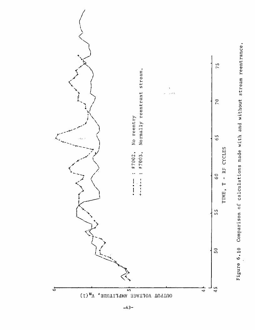
a, k c, vl
. . N M 0 0 0 0 b b * * .. ..
I I e +
-43-

- 44-
JUNE 25, 1968 sm. NO. 6007 STEP NO. 961 TIME 95.993
+ + + + + + + 2 $3 f $ " + + + + ++ + 1 +++ H ++*+$ s++*s ++++++ + + ++-I-++* $++++$ +++++$ $++++is * * * * * *
*H * * ** * * ** * * * * * * *
** * * * * * * * * * * * *
$ + + $ $ $ $ z t $ 1 + + + + $I-++++ ++++I- +I-++++ ++++++ +++++$ It++++$ + + + +
* * * * ** * * * * * * * * * * * * * * * * * ** * * * * *** $* ** * * H A * z * *
H J + + + + 1 + ++++f+++++-l-+++i-t-H4i-t++++++++++++++++++++++++~ +++++++ ++++
Figure 6.11 Calculation #6007: Configuration a t T = 96.0
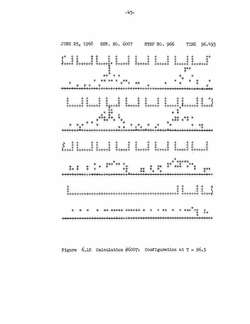
-45-
JUNE 25, 1968 S'ER. NO. 6007 SmP NO. 966 TINE 96.493
+ + L++$ $' $ $ + i $ $ " $ 1 $ $ $+-I-+++$ +++++ ++++++ +*+$ ++++++ ++-I+++ +++*
+ + + + + * ** * * * ** * * * * * * ** ** * -&!+ * * * * * * * * * * * * * * * * *
( 1 1 , , I I , $ 0 1 8 1 1 , , , 1 1 1 , 1 , , , , , , , , , , , , , , , , ~ I I , I , I 1
+ + + -I-+ + $ $ i$ + + +
+ + + + + + + + + + 2 $ + +*+ $+-I-+++$ $++++$ L*+ +++++s $+-ttt+ +++I-+ ++-I++++
* * * **H * I** 3Hc * ** * ** * * * * * * * * * *** * * *** * * ** H * * * *H * ** * * * c : : : : : : ! : ! : : : : : : : : : : : : : : : : : : : : ! : +
$ $ $ $ f 5 *+++++-l-l-++++++++++++++++-l-t+*-l-l-+++++++++++++ +++I-+++ ++++
Figure 6.12 Calculat ion #6007; Configuration a t T = 96.5
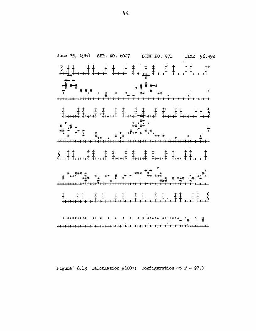
- 46-
June 25, 1968 SER. NO. 6007 STEP NO. 971
i f $ $ $ $ ' $ $ + + + $ $ -t+-Ry;+++++++ ++++++ ++++++ ++%* fl-l-t++ ++++ ** *
* * * *
I * * * M * * * * jcJc ** * * *
TIME 96.992
$+ + + + + +++++++ $ $
* *
cM.::::!::::::::::::::::::::::::::::::::::::-tt.::::~:,::::t
* * * jcJc* e* * * * * * * *
* * * * * **,w * 'I * * * * **** * * * * ** * *** * * * *
* * * Y
*wWHHw * * * * * * ****e** * * * * * * +-: : : : : : : : : : : ;3fw-: : : : : : I - : : : : : :~*: : : : : : : : : : : : m: : : : ! : : : : : k
Figure 6.13 Calculation #6007: Configuration a t T = 97.0

Figure 6.14 shows the i n t e r n a l r f vo l tage and r f induced cur ren t d i s t r i b u t i o n on the network. 6 . 4 are absent here, ind ica t ing absence of appreciable mismatch. Further evidence of t h i s is the f a c t t h a t t he input e lec t rode , #24, is c lose t o t h a t of t h e inc ident s igna l . There does, however, appear some vol tage disturbance having a slow space-variation. i n s t a b i l i t y discussed i n Section 6.2.3; t h e disturbance propagates and appears as an o s c i l l a t i o n of t he output s igna l amplitude.
Severe standing waves as shown i n Figure
This i s a symptom of t h e
Figure 6.15 i s an histogram of the co l l ec to r data. These are sketchy; averaging over s eve ra l cyc les would improve them. There appears t o be a grouping of co l lec ted p a r t i c l e s a t low po ten t i a l s . This must be viewed with caution, however, as i t is probably exaggerated by t h e ar t i - f i c i a l demodulation process.
6.4 Effec t of Parameters on Operation
It has not been poss ib le t o cover t h e e n t i r e range of parameters The discussion below is necessar i ly incomplete, particu- thoroughly.
l a r l y with respect t o high ga in conditions.
6.4.1 D c Anode Voltage
Operation as a func t ion of dc anode vol tage i s of i n t e r e s t because of t he e f f e c t of e l ec t ron stream velocity--and hence on the traveling- wave interaction--and a l s o because of e f f e c t s on emission from cathodes (magnetron ti Amplitron) .
The dc anode vol tage w a s increased from the Hartree l e v e l t o 10% above it a t an e a r l y s tage i n the ca lcu la t ions . no e f f e c t on gain o r power output a t t he 6 db gain l e v e l obtained a t t h e t i m e . The amplifier w a s c lo se t o sa tu ra t ion , and small-signal ga in conditions were absent. The increase i n dc anode voltage, 1.25 Vo, w a s i n t h i s case somewhat less than t h e peak input voltage, which w a s 1.78 Vo. e f f e c t a t lower power l eve l s .
There w a s p r a c t i c a l l y
It i s p o s s i b l e t h a t v a r i a t i o n s of t h e dc anode voltage have more
The p r inc ipa l changes noted with t h e increase i n anode vol tage w e r e reduction i n e f f i c i ency (because the dc input power increased without increase i n r f output) and a small change i n output phase. This phase- pushing due t o dc anode vol tage w a s approximately -1.3' p e r 1% increase i n the anode voltage.
6.4.2 D e In jec ted Current
Increasing t h e in jec ted cur ren t provides g rea t e r stream curren t , This increases t h e ga in and corre- o ther f a c t o r s remaining constant.
spondingly shortens the small-signal region, lengthening t h e sa tura ted region (or causing one t o appear i f a t t h e verge of s a tu ra t ion ) . 6.16 shows t h i s .
Figure
The stronger r f f i e l d s shorten t h e t r a n s i t t i m e t o t he anode f o r favorably i n t e r a c t i n g e lec t rons , however, tending t o provide an o f f s e t t i n g
-47-
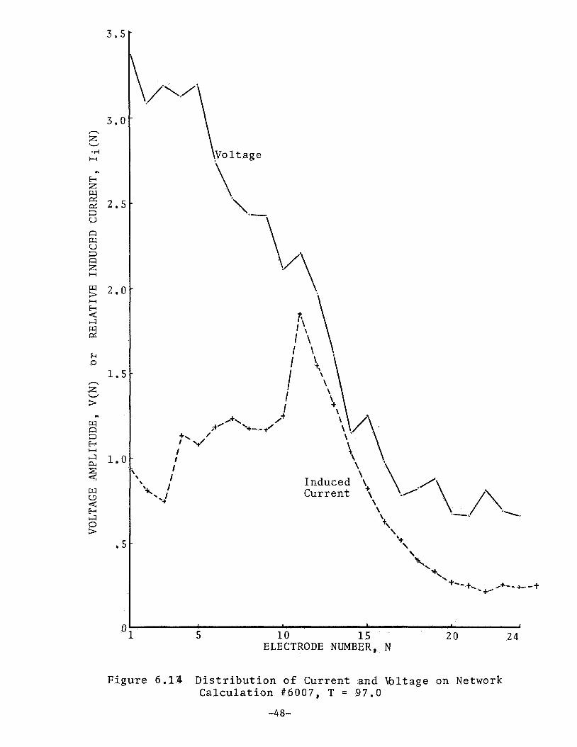
3.5
3 .0 n z u H .?I
a
E-r z 2 a: 2.5
n
3 U
w U 3 n z H
5 2.0
2 I--I b
w p:
k 0
1.5 n ,z s
w n 3 E-r
W
L
H
IJ 1 . 0 % W W
crl 0 > 2
. 5
0
\
I I I
I t \ \ \
I I
M+\ 0t ,t' '++-..+/
I I I ' I
' I '%. I '+
1, \ \
Induced \+ Cur ren t \
'+ \
I
5 10 1 5 20 2 4 ELECTRODE NUMBER, N
F i g u r e 6.1% D i s t r i b u t i o n o f Cur ren t and I b l t a g e on Network C a l c u l a t i o n #6007, T = 97.0
-48-
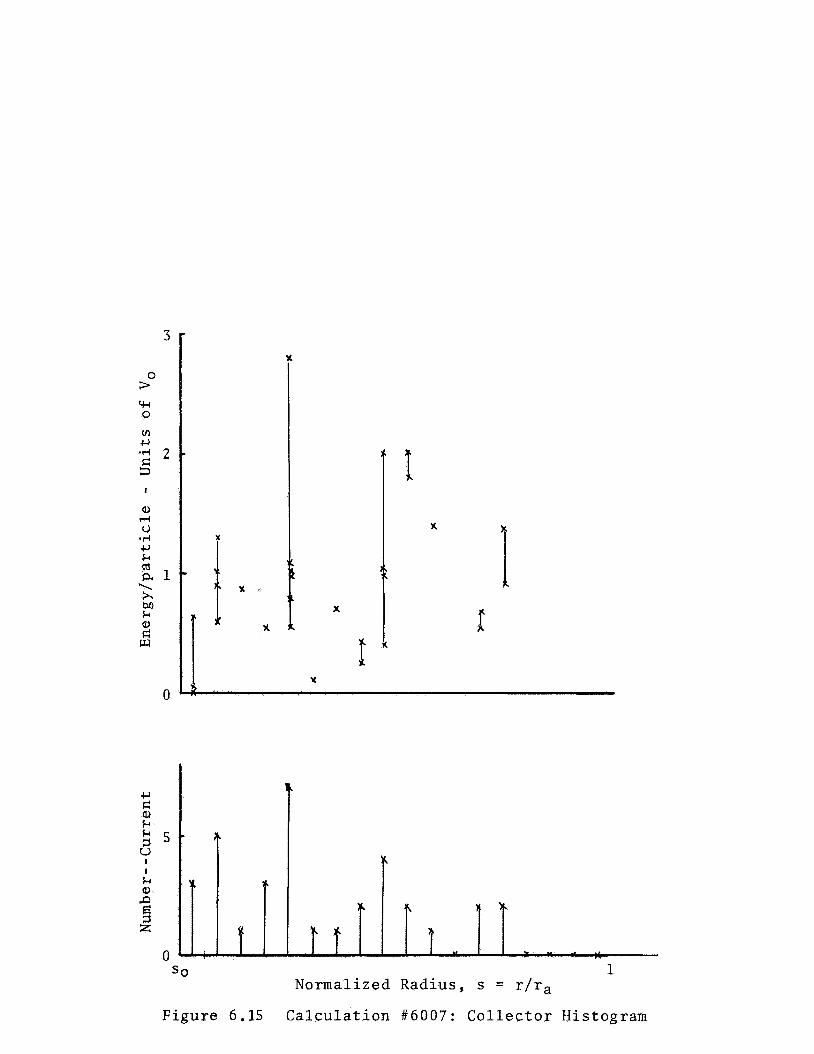
SO
x - I x I x
1 Y
1 X
f
L 1
Normalized Radius , s = r/ra
F i g u r e 6.15 C a l c u l a t i o n #6007 : C o l l e c t o r Histogram
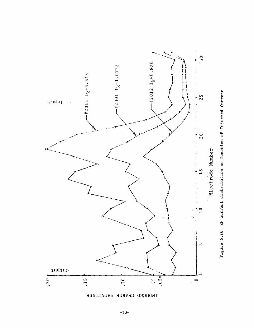
0 N
v) d
0 4
-50-
0
u
k )-1 3 W a aJ u CJ a) ‘r) 0 H
w 0
$
-4 U z $
5 w
c 0 rl u 3 P -4 k U v1 -4 “ct U c a) k (-I 3 u
3 \o
\o
4
k ;r;f 5 M

reduction i n the t o t a l stream curren t . Furthermore, t h e unfavorably focused e l ec t rons ga in more energy from t h e stronger r f f i e l d s , and sole cur ren t is l a r g e r . Another f a c t o r complicating t h e e f f i c i ency p i c t u r e is t h e f a c t t h a t because t h e large-signal region is longer, the e f f i c i ency is higher. Figure 6.17. This p l o t , even more importantly, shows t h a t t h e output s igna l is l i n e a r l y r e l a t e d t o t h e in jec ted cur ren t .
The p l o t of computed e f f i c i ency is shown i n
Use can be made of t h e r e l a t i o n shown between r f output and in j ec t ed cur ren t by using i n conjunction with i t t h e r e l a t i o n between t h e r f level and the i n j e c t i o n cu r ren t , as reported experimentally. This information i s not known here. The a c t u a l in jec ted cu r ren t , t o t he ex ten t t h a t i t is cont ro l led by t h e r f f i e l d s extending from t h e network toward t h e cathode, i s probably sor ted by the process. appear t o be similar t o provision of a prebunched beam i n a traveling- wave device. There are many unknown f a c t o r s involved, some of them rq i s ing questions as t o t h e adequacy of t he two-dimensional model used here.
It thus would
The computations showed a phase-pushing due t o in jec ted cur ren t v a r i a t i o n of +O . 3 O / I O .
6 . 4 . 3 R f Input Power Level
The r f power input was reduced t o take t h e amplifier from the satu- r a t i o n region of its operation toward the l i n e a r region. Figure 6 .18 shows the network r f cur ren t d i s t r i b u t i o n as t h e power level w a s reduced from 3.5 t o ,2. The disappearance of the sa tura ted region within the i n t e r a c t i o n i s clear. The input-output r e l a t i o n f o r t he amplifier i s shown i n Figure 6 . 1 9 . encountered as t h e input power l e v e l w a s reduced. because of the feedback problem noted i n Section 6 . 2 . 3 .
I n these ca lcu la t ions progressive i n s t a b i l i t y w a s This is probably
In one trial ca l cu la t ion the r f l e v e l w a s reduced t o about 20 db This level i s about t he below t h e output levels here tofore observed.
level of vo l tage induced by the reenter ing r f stream curren t . The cal- cu la t ion w a s s t a r t e d from empty in t e rac t ion space, with t h e r e s u l t shown i n Figure 6.20. Large-signal conditions appear ra ther quickly i n s p i t e of t he small input s igna l and the amplifier--probably because of stream feedback--behaves as an injection-controlled (locked) o s c i l l a t o r .
6 . 4 . 4 Rf Impedance Level
Most of t he in jec ted beam forward-wave amplifier ca lcu la t ions were made f o r a c h a r a c t e r i s t i c impedance at reference frequency equal t o 400 ohms; t h i s corresponds t o an i n t e r a c t i o n (coupling) impedance, EE*/2B2P, of 160 ohms at t h e anode surface. A few ca lcu la t ions w e r e made f o r the higher design va lue of 200 ohms. The r e s u l t s are compared i n Table 6.5.
-51-

INJECTED CURRENT, I k
F igu re 6 . 1 7 E f f e c t of I n j e c t e d C u r r e n t .
-52-
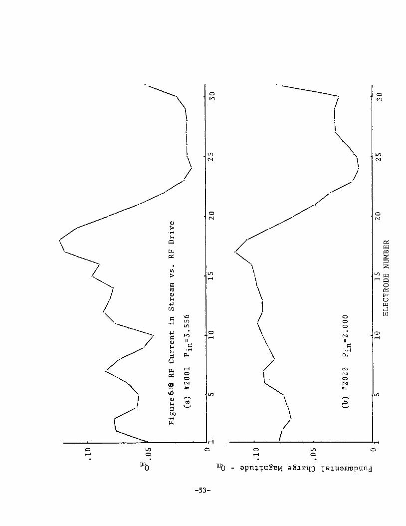
0 rl . Ln
0 . "b
C
1 I I
i i.
I i i \ i i \ i i
i \ i
0 rl . In
0 .
0 0 0
N I I
.rl a, F:
c\I N 0 N *
0 M
Ln N
3 u
d w Fz? 2 3 z
n w -(n 0 d F* U w Cll w
3 -4
n
-I
c
-53-
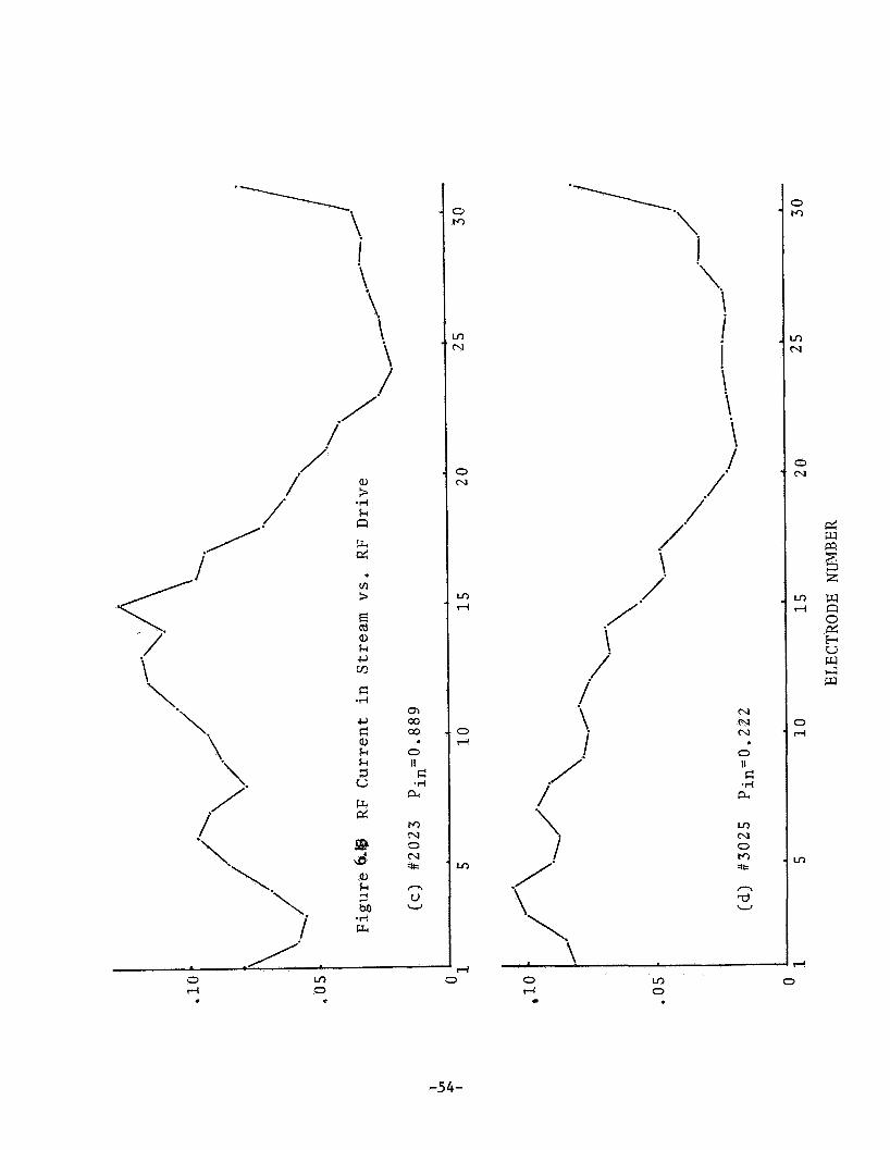
I i i \
/- i i i
/ /-
v) * i
Fi a, k
*< ’/ i
I
c, v?
E: *d
E4 d
P d
m co co 0
I I
.r( E: a
M r\I 0 N =tk
n u W
3 rl
In 0
./ \
L n i / *
\ i i \
/-
rl
i 0 rl
i \ i /
\. \
\ rl
3 0 rl
Ln 0
h3 N N
0 l l F: .d a
Ln N 0 M * n a U
0
-54-
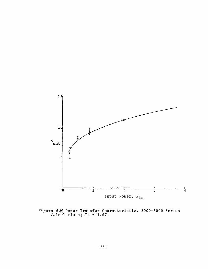
1
1
Pout
I
1 ‘ 2 3 4 Input Power, Pin
Figure ‘6.19 Power Transfer Characteristic. 2000-3000 Series Calculations; Ik = 1.67.
-55-

C a l c u l a t i o n h170
I
0 5 1 0 1 5 2 0 TIME, T - RF CYCLES
F i g u r e 620 S t a r t - u p t r a n s i e n t w i t h very small rf i n p u t s i g n a l
-56-

Table 6.5 Effec t of Network Impedance
Run No. 4012 7003 Charac te r i s t i c
Coupling
In jec ted cur ren t 3.75 3.75 Anode cur ren t 2.50 Rf input Rf output Gain 7.9 8.9 db
impedance 400 500 ohms
impedance 160 200 ohms
The higher network impedance r e s u l t s i n higher c i r c u i t f i e l d s , tending t o overcome space-charge debunching e f f e c t s ; i t i s therefore advantageous. No optimum impedance level w a s observed. Such an optimum probably does e x i s t , however, s ince excessive t ransverse v e l o c i t i e s would r e s u l t , and t h i s would ind ica t e high anode bombardment and lowered e f f i - ciency. It probably would be to l e ra t ed only i f t he re w e r e no b e t t e r way t o ge t higher power.
6.5 Second Design of the In jec ted Beam Amplifier
A s i n the design of magnetrons and other crossed-field devices, t he re e x i s t s some degree (not excessive) of freedom i n meeting the objec- t i v e s . By s u i t a b l e choice of dimensions and mode number, t he sca l ing vol tage can be var ied over a considerable range. Similarly, t he sca l ing cur ren t can be var ied so t h a t the device can be a low impedance one o r high. This is e spec ia l ly use fu l when one encounters space-charge e f f e c t s t h a t l i m i t performance, as by dc cur ren t l i m i t s o r spurious o s c i l l a t i o n s o r noise. t h e ana lys i s t o determine these l i m i t s , of course, and t h e l i m i t s are most genera l ly s t a t e d i n normalized terms as has been done i n t h i s repor t .
Use of sca l ing techniques i s common.
It is t h e function of
The second design of t h e in jec ted beam ampl i f ie r raises the anode vol tage and lowers the cur ren t l eve l . The mode number w a s increased from 7.5 t o 16; t h i s reduces the azimuthal e l ec t ron ve loc i ty and hence reduces t h e sca l ing magnetic f i e l d , Bo (cf Table 6.3). magnetic f i e l d , then, t he synchronous (Hartree) vo l tage i s much higher (esp. when normalized) and higher e f f i c i ency i s indicated. a depressed s o l e is used; t h i s should make i t v i r t u a l l y impossible f o r e l ec t ron in t e rcep t ion there.
For a given applied
I n t h i s design
The computer program was again r ewr i t t en t o allow f o r t h e l a rge r num- ber of e lec t rodes . It w a s used both with a r t i f i c i a l and with physical demodulation of the reenter ing stream; some r e s u l t s are shown i n Table 6.6.
-57-
I * i
5 10 15 20 24 ELECTRODE NUMBER, N
Figure 6.21 Calculation #7004 : Internal voltage distribution T = 19.5
Table 6.6 Calculations with High Mode Number (Second Design)
Run No. Anode vol tage In jec ted cur ren t Axial t r a n s i t # of anodes I f active anodes Coup1 ing impedance Network l o s s Rf input power Ef output power Gain
5000 27.8 1.67 10 64 52
.7 3.6 24.9 8.46
5010 27.8 1.67 10 64 52 160 .7 3.6 22.8 8.08
501 1 27.8 (Hartree) 1.67 10 cycles 64 52 160 ohms .7 db 2.0 21.8 10.4 db
The charge configurations are shown i n Figures 6.22, 6.23, and 6.24.
These ca l cu la t ions appear t o be r e l a t i v e l y f r e e of t h e i n s t a b i l i t y t h a t w a s so troublesome i n ca l cu la t ions of t h e f i r s t design. considered t o be t h e r e s u l t of b e t t e r demodulation i n the d r i f t region, which is longer and which allows e l ec t rons t o move t ransverse ly toward t h e so le . The e f f i c i ency f igu res obtained are suspect; poor energy balance w a s encountered. The ca l cu la t ions should be made with a smaller t i m e i n t e r v a l ; t h i s is c o s t l y because of t h e high mode number.
This is
7. CONCLUSIONS OF PART I.
7.1 Conclusions
Computer r e s u l t s f o r r e l a t i v e l y low ga in operation (6 t o 12db) of t h e in j ec t ed beam forward-wave amplifier were obtained. gain can be increased by increase of in jec ted cur ren t and/or r f impedance l eve l . Stream feedback is important i n regard t o high gain, but moderate ga in can be obtained f o r a wide range of feedback conditions.
They show t h a t
Some ca l cu la t ions w e r e car r ied through f o r higher ga in conditions, but t hese were r e s t r i c t e d by appearance of i n s t a b i l i t i e s i n t h e computa- t i ons . After considerable e f f o r t , i t w a s concluded that t h e i n s t a b i l i t y w a s caused by stream feedback. i n the e l ec t ron tube and the computer model of it are needed.
Means f o r eliminating t h e feedback both
7.2 Recommendations
Further study of t h e ampl i f ie r i s needed t o answer t h e questions l e f t unanswered here, v iz . , questions as t o t h e e f f e c t s of varying the magnetic f i e l d , t he frequency, on the amplifier performance. More thorough explora t ion of t h e range of va r i ab le than has been poss ib le i n t h e present l imi ted program.
More bas i c questions need t o be answered concerning t h i s new amplifier. cur ren t and t h e axial t r a n s i t ve loc i ty? t h e d r i f t region? t h e co l l ec to r? t h e network? Any f u t u r e work should be done by those i n a pos i t i on t o obta in t h i s information.
Typical are: how does t h e r f f i e l d influence t h e i n j e c t i o n What are the p rec i se d e t a i l s of
It i s not
-59-

- 60-
JUNE 28, 1968 SER. NO. 5010 STEP NO. 408 T W 40.797
~~~~~
f
H * ** * * * *H * * * w*** * * * * * w 3 w H c * * * * * * * * * * * * * * * * H * * * * 4 : : : : : ! : : : H 4 H 4 - k : : : :-cwct: ! ! ! : : : : :-: : ! : : : ! :.l-H+tl!: : : : : : : : : : i-
* * * * * * * *
xsc ** LU * u r n Lg-JLKJ: :Ts: :m: :nit * ** *xsc * *H * * * * * *w ** * * xsc
* * * * ** * -*'** * * * * * * * * * ** H* *** * * * -wx. * * * * * *
4 ! : . : - :* : . : : : : : :~.H-CH-H!:: : : : : : : : : : : : : : : : : : : : : : : : : : : : : : : : : : : ! I -
H k .3Hc *w* * * * * *
* m *H* * * ** * * *
* * -we* ***- * -wx. * H * *
Y *
** *" * * * * * **H*** **** H** * H * *
* + * * + ! :.: :~-*: : : : : : : : : : : : : : : : : : : : : : : : : : : : : : : : : : : : : :
* * * * * x3c ** * ** --v* * *** *** &** ~ * * * ** * * *M* * * * * * * * * * * * * * *
t+t.:::,::::::::::::::::::::::::::::tct-:::::::::::::::::::::::.I-
Figure. 6.22 Calculation #5OlO: Configuration a t T = 40.8

- 61-
JUNE 28, 1968 SER. NO, 5010 STEP NO. 412 TIME 41.197
** * * ** * ** * * x-x)c * * * * * ** * *w -)wc * * * * * * * * * * * * ** * * ** * * * * * * * * * * * *
* ~~~~~~~ * * ** * * *
Jc;w. * Jc3t3c
w u w I;TuI! :TT:LV: !I * * ** * m * * * * Jc;w. ** ** ** ** ** ** * * * * * * * * * * * , * * * * * * * * ** * * * *
4 : : : : : ; : : : : : : ; ::::;:::;::::;:sHf.::;;:::::::::!:::::::~:::!::
x 44 )c3c *'. * *"** *
)oHc* **M** * 3cJc *-*** ** -n;xsc*
* * M * * * * * * w + * *** jcjcjc ** * * *** * * * * .x * -+:::::;::::::ctt::::::::::: I : : : : : : : : : : : : : ! : : ! : : : ! : : : : : :-w-cw.
,. I.
YY.' 4 Y .3Ht***"jiSc* %-% ** * * * * *** z*c.A.mc * * * ** m **** * * * * * * * * * ** * * * * * * * **
Figure 6.23 Calculation #golo: Configuration a t T = 41.2

-62-
-&. ++ ++ + I- ++ ++ ++ ++ .t+ ++ ++ ++
JUNE 28, 1968 SER. NO. 5010 STEP NO. 418 TJMF, bS.797
n * * ** M * * * * * * * * * * *
** ** * * * * * 3HC * *
* * * * * * * * *
**
* -w * *
* * * * *
-I ! : : : ! M::::::.:::::::,::!:::!:!::::::::! : : : : : : : : : : : : : ::::::u-t
* * * * *** * *H * * *
* * ** * * H* * * M m -w * * **** * * **** * * * - w * * * * * * * * * * * * * * * * * * * * * * ** * w.
d ! : ; : : : : : : : : : ,: : : : : : : ! : : ! ! ! : $-H-H-cccw-w ! : : ! b : : : : ! : : : : ! ! ! ! ! ! : I-
* * ** ** xst .# 7W-H- * ** H-** ** * * * * * * * * *w* *-w* * ** ** * *-w * * -w ** -w* *
* - w * * * * * *** * * * *
+: : ; : : : : ! : ! : : ; : : : :.: : t", ; : : : : : : : : :.: ,: : : : : : : : : ! : ! : : ! : ! : : : : : ! ! ! ! : I-
* * 3cJe *M** * *** * * * * * *
* -H@x-E+E+Jc-)t. * * w* w** -+E+ * * * * * * * * * * = * * * * * * * * * *
i:::::.::::::::MtM-Ht:::::::::::::: ::::::::iS+fct: : : : : : : : : : +
Figure 6.24 Calculat ion #5010: Configuration a t T = 41.8

realistic to expect useful results from isolated analysts. E.g., the computer at best will only tell one what happens when certain parameters have certain values. They do not generally tell one what values are the best ones to use; this information can best come from the experimentalist.
It may also be possible that the transient/simulation method may not work under conditions of eevere space charge, as difficulty has repeatedly been had in the magnetron situation. putational technique should be used, e.g., those used by Rowe et al. at the University of Michigan.
Perhaps some other com-
-63-
PART 11. AMPLITRON NOISE MEASURENENTS
8. INTRODUCTION
This p a r t of t h e research program is t o evaluate t h e noise c h a r a c t e r i s t i c s of a commercially ava i l ab le Amplitron, t he Raytheon type QKS-1300. Two such tubes (nos. 156 and 185) were supplied by NASA. This tube has an output power r a t i n g of 25 watts.
Sources of no ise i n ampl i f ie rs f a l l i n t o two classes: (1) those of a con t ro l l ab le nature, and (2) the uncontrollable ones. The former includes power supply r ipp le , microphonics and outs ide in te r fe rence . A well-designed system takes the necessary precautions aga ins t these sources and is l imi ted only by economics. sources w i l l not be made.
Further discussion of these
The uncontrollable sources are l a rge ly t raceable t o t h e cathode and i t s random emission of e lec t rons with random v e l o c i t i e s . Cathode f l i c k e r These components of noise are usua l ly very broad band, whereas the con- t r o l l a b l e ones are usua l ly characterized by frequencies r e l a t e d t o t h e frequencies characteristic of the r i p p l e o r o ther d i s turb ing forces. When resolved i n t o a-m and f-m components, a co r re l a t ion between t h e a-m and f -m components o f t en exists.
noise and p a r t i t i o n noise a l s o appear i n microwave tubes.
The purpose of t h i s research, however, is not t o inves t iga t e the sources of t h e noise, but t o measure it.
9. MEASUREMENTS
9.1 Scope
Since the Amplitron is t o be used as a transmitter device r a the r than, say, a l o c a l o s c i l l a t o r , t he noise must be measured over a wide range of frequency from seve ra l t ens of megahertz from t h e carrier t o as c lose t o t h e carrier as possible--on the order of a few kHz. To def ine the noise adequately, a r e so lu t ion i n t o a-m and f-m noise is required
9.2 Measurement Techniques
The no i se measuring system must be capable of measuring very low
While i t is poss ib le t o reject a strong s igna l with a pre- l e v e l s i g n a l s ( the noise) i n t h e presence of a very strong one (the carrier). se l ec to r , (which is not r e a d i l y ava i lab le , anyway), t h e s e l e c t i v i t y required of such a device t o d iscern noise wi th in a few KHz of the carrier is impossible t o a t t a i n . prevent t h e carrier s igna l from entering t h e measuring system lest it
An a l t e r n a t i v e scheme is required t o
swamp" t h e noise t o be measured. I t
The method used here cons i s t s of use of t h e bridge arrangement shown i n Figure 9.1. ampl i f ie r is balanced aga ins t the output s igna l i n amplitude and phase
I n t h i s arrangement, t h e input s igna l of t he
-64-
n
4
d w E-.
22 4
H
H
-65-
so t h a t t h e carrier s i g n a l is nulled. measured by t h e de t ec to r is the noise and o ther spurious s i g n a l s gen- e ra ted wi th in t h e ampl i f ie r under test. I n t h e present case, t h e phase adjustment is made by v a r i a t i o n of t h e probe pos i t i on i n t h e s l o t t e d l i n e i n the input arm. The amplitude adjustment f o r balance is made i n the a t t enua to r connected t o t h e branch which samples t h e output arm, i t s e l f connected t o a high power load.
The only s i g n a l remaining t o be
Among t h e d i f f i c u l t i e s of t h i s technique i s t h e f a c t t h a t t h e probe must be s u f f i c i e n t l y deep t o couple appreciably so t h a t t h e noise s igna l fed i n t o t h e de t ec to r may be l a r g e enough t o be observed. On t h e o ther hand, t he degree of coupling must not be so l a r g e t h a t a s igna l be fed back i n t o t h e input l i n e from t h e output l i n e o r so deep that ser ious mismatch be caused i n the input l i n e . These measurements were made with- ou t any apparent d i f f i c u l t y from these f ac to r s .
Measurements are made with t h e system as shown, and a l s o with a limiter placed i n the output a r m s i g n a l path. y i e lds t h e t o t a l no i se measurement; the lat ter, only the f-m pa r t . The a-m no i se power dens i ty i s determined by d i f fe renc ing t h e two.
The former measurement
The no i se measured by t h e de t ec to r a f t e r carrier cance l la t ion is rendered i n absolu te terms by a c a l i b r a t i o n procedure i n which a known power l e v e l from a s igna l generator i s pagsed d i r e c t l y i n t o t h e de t ec to r ( a Tektronix type 1L20 spectrum analyzer) having s u f f i c i e n t bandwidth t o accept the s igna l .
The noise power s p e c t r a l dens i ty measurement i s limited by t h e pre- sence of the r e s i d u a l carrier and t h e prospect of i t s passing i n t o t h e spectrum analyzer. The frequency "jitter" of t he input s igna l w a s a t b e s t + 3 kHz; t h e spectrum analyzer bandwidth w a s ad jus tab le i n s t e p s downward t o 1 kHz. Thus, t h e noise measurements can be considered use fu l t o within approximately 5 4 kHz. of t h e carrier.
9.3 Results
9 . 3 . 1 Preliminary Measurements on S e r i a l No. 185
It w a s o r i g i n a l l y planned t o perform complete measurements on two '
Amplitrons. The f i r s t tube t e s t ed (Jj185) f a i l e d , however. It exhibited spurious o s c i l l a t i o n s when operated, and on cold test showed a l a rge i n t e r n a l r e f l e c t i o n . Permanent damage had apparently occurred. Gener- a l l y , i t w a s observed t h a t most of t h e noise is wi th in a few kHz of the carrier frequency. Over a broad spectrum of several MHZ about t h e car- rier--mostly described by the pass band of t he Amplitron network--there w a s some "white" noise. temperature; even s f n a l l changes i n hea ter cu r ren t produced severe changes i n t h i s background noise level.
This no ise w a s s t rongly dependent on cathode
9.3.2 Measurements on S e r i a l No. 156
Noise i n t h e second of t h e two Amplitrons was a l s o dependent on hea ter power, hence on cathode temperature. Figure 9.2 shows the t o t a l
-66-

* .
Mu) N C V
rlrl
II II
. .
& S H H .. .. I I o m I ! O C I
I I a
I I I I I
P
I I I 1
0 x i I
I I I I
I 1
I I I
0 e
I
0 In
I
\ \
I 1 t I I I O I I
0 \o
I
Q
\ I 0
0
1 I I I 1 I l 0 4
‘ 0 b
I
I
1
r<
!f
r(
f I I I 1 I
I 1 x I I
e, v,
. s i
0 z F: 0
c, F: a, k k 3 U
k a, c, cd a, =e %I 0
c, u a, w w w
N
a a, k =f M *.-I E4

noise spectrum dens i ty when the Amplitron is operated under ra ted operating conditions with t h e optimum hea ter cu r ren t , Ih'1.23 de amperes, and with a s l i g h t l y d i f f e r e n t hea te r cur ren t . noted t h a t the p lo t t ed frequency scale changes a t 100 K H Z f o r the sake of convenience. Beyond 100 KHz from t h e carrier, t h e noise is essent i - a l l y "white." Amplitron "cold"; t h e r e s u l t s shown ind ica t e t h e limits of measurement r e l i a b i l i t y . Clearly, t he noise i n excess of -75 dbm/Hz can be d i s - cerned a t frequencies a t least 10 KHz from the carrier.
It should be
For reference, t he measurement w a s repeated with t h e
It is perhaps premature t o draw s i g n i f i c a n t conclusions from the hea ter power dependence of t he noise, s ince the tubes t e s t ed were both known t o have thermal p e c u l i a r i t i e s , having been r e j ec t ed by the manu- f a c t u r e r on t h i s account.
Measurements w e r e a l s o made with normal r f d r i v e power and with very small dr ive . The r e s u l t s are shown i n Figure 9.3. The f a c t t h a t no peaking of noise occurred a t t h e carrier frequency probably means that t h e Amplitron w a s not locked t o t h e d r ive s igna l . t h e noise observed i s probably a l l thermal noise from the cathode, with no car r ie r -assoc ia ted noise (which would have strong f-m components as w e l l as a m ) . carrier appears when the d r i v e l e v e l i s r a i sed t o normal l eve l s .
I n t h i s case,
The l a r g e noise l e v e l i n the 50 KHz band around t h e
Inse r t ion of the limiter i n t h e bridge as shown i n Figure 9.1 produced t h e r e s u l t s shown i n Figures 9.4 and 9.5. Figure 9 . 4 t h a t t h e noise measurement is ser ious ly upset near the carrier frequency, and t h a t t h e measurement with the Amplitron operating conse- quently has l i t t l e meaning. It i s thought l i k e l y t h a t the limiter i t s e l f i s a source of considerable noise.
It would appear from
9.4 Conclusions
The carrier cance l l a t ion system using a s l o t t e d l i n e proved usable f o r measurement of t h e t o t a l no ise power dens i ty of t he two Amplitrons t e s t ed . The noise power dens i ty w a s measured at frequencies t o within 10 HHz of the carrier; t h e r e s u l t s are given p r i n c i p a l l y i n Figure 9 .2 . They show t h a t t h e noise level i s -68 dbm/Hz f o r frequencies more than 75 KHz from the carrier, r i s i n g t o approximately -58 dbm/Hz at 10 KHz from the carrier. There is s l i g h t asymmetry i n the spectrum.
Measurement of t h e purely f -m component of t h e noise w a s not possi- b l e because of system de fec t s which are thought t o be l i m i t e r noise.
-68-
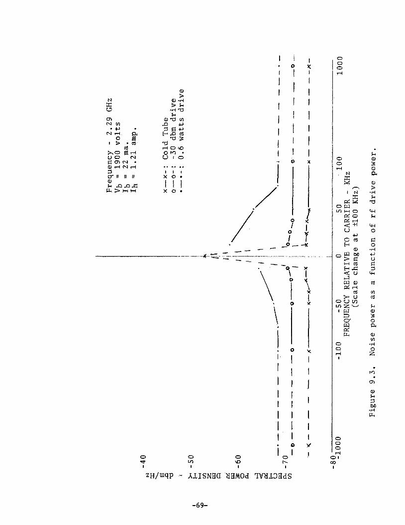
N :
(I) t r l
S k *d a k
a,* v) P c , S E c , ba cd
- 3 a dO\D O M * u t 0 .. .. .. I l l
X O .
I l l X O . ,'
i 0
f
J I I I I
I
0
0 I
I 0
I Y I
I I I 1 I I I x
P T r< I
\ \.
I I . I I I I I I t * I
i 0
0
I I I I I 1 I 1 0
i 't Y
I K
x 1 I I I
I I I Y
I
-69-
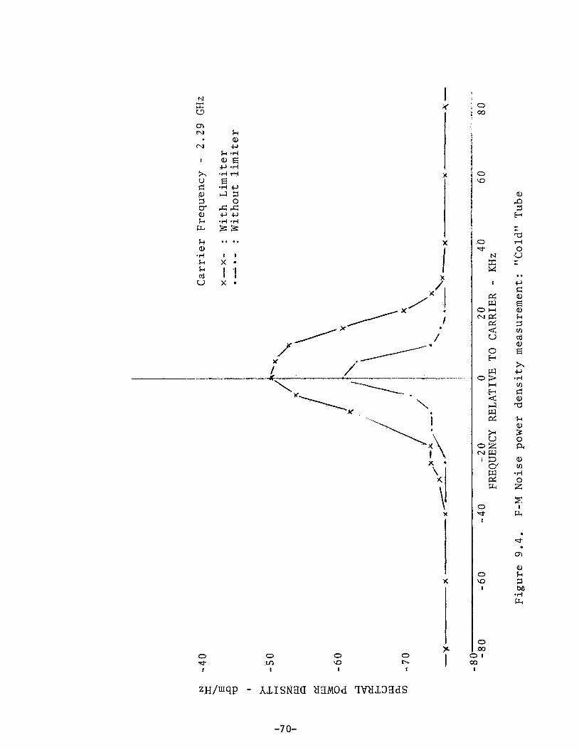
I
\ K
I Y
x
X i
\ I
0 d
t
0 VI I
0 W I
0 t-
f
x
x
0 W
0 u-
N 3: w I
d W
N d d
O H
5 0 b
W 0 s b
W d
H
2
G 0 2 N W
1 3 cy W d L
0 d I
0 W
1
0 co
> I oc) I
-7 0-

k a, c,
I t x *
I i X I
"I I
I I
0 0 In a
I I
8 ! 0 I-
1
0 oc) +
i !
-71-

APPENDIX A. COMPUTER PROGRAM LISTING
A p p e n d i x A . l L i s t i n g of C o n t r o l P r o g r a m
c c
10
1
4 h ?
3 (53
4 1.
6 3 ' 41)
51 6 4
65
52 410
66
-7 2-

-73-

Appendix A . l . l Timing Subroutine (IBM 360 Assembler Language)
-74-

Apgendix A.1.2
AGN T S T
PUT
T I T L E ENTPY
D b f E S h V E BBLP USING L L L T I M € i WP L W R S R b SLA 4R ?-T SR S T ST CVR < T ZT C V B ST LA i C RNL b B L
F T S R A ST c ST
c
-7 5-
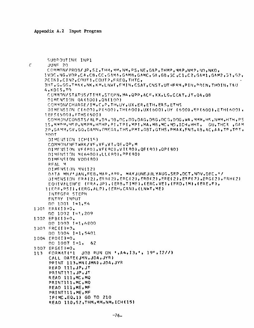
Appendix A . 2 Input Program
T o r J V.D€C* '
-76-

-77-
-78-
-7 9-
Appendix A. 2 1
2 9
7 5
3 9 3 5
40 4 5 46
48
5 0
55
-80-

I - <’ ‘1
7 3 75
Q P
l ’ q 12n
1?’5
3?0
a 5 3
-81-
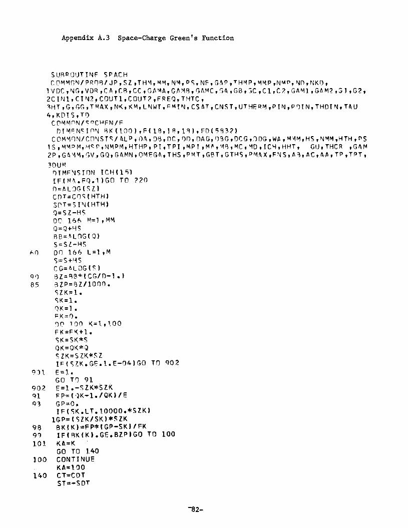
Appendix A.3 Space-Charge Green’s Function
‘82-
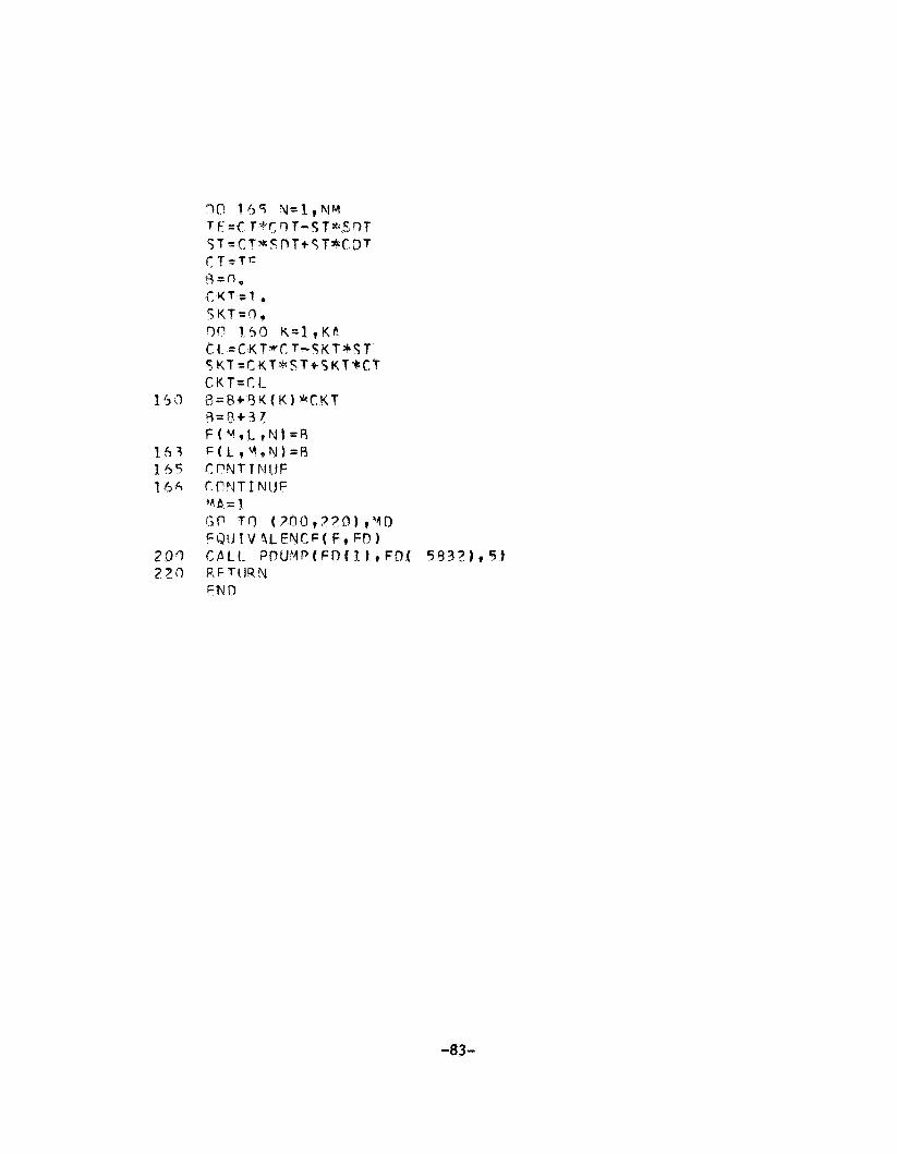
-83-
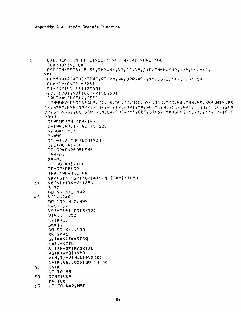
Appendix A.4 Anode Green's Function
-84-
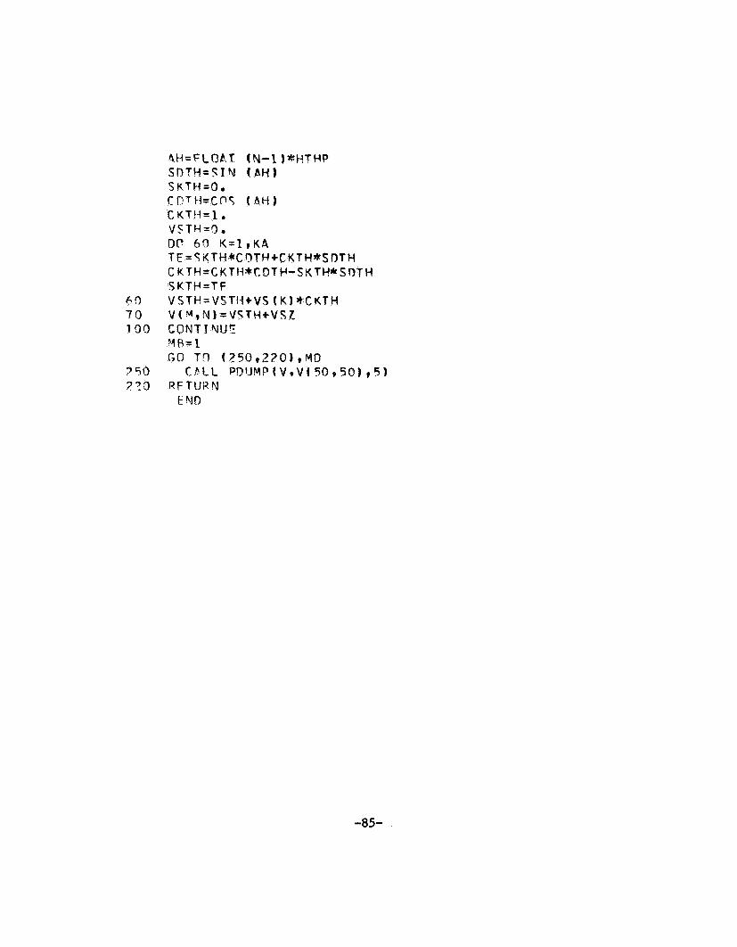
-85-
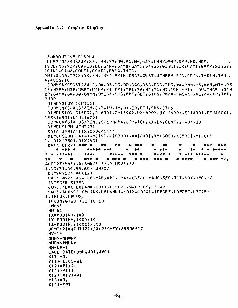
Appendix A.5 Graphic Display

-87 -


Appendix A. 5 . 1
-89-

Appendix A . 6 Space-Charge F i e l d Calculation
-90-
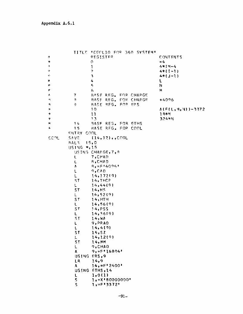
Appendix A. 6.1
C !3n3 T F Y T 5 =4 45 r Y - 4 4 w I - I 1 4*( J - 1 ) L M M
-91-
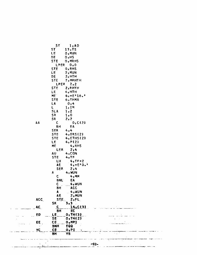
S T 19AD ST 13 ,TS LF 0 q MUN DE O,HS STE OqMRHS
LPER 090 STE OqRHS LE 2 9 MUN DE 29 HTH STE ZqMRHTH
LPER 2 9 2 STE 2,RHTH LE 6pHTH ME 6 9 = E ' 16. ' STE 6,THMX LA 094 L 1 p I M SLA 1 , 2 S R 1 9 0 SR 2 r 2
A A C O,C(2J BH EA
SER 494 STE 4,ERStZ) STE 4vETHSf21 LE 4 r P ( 2 ) ME 4 q R H S
L E R 294 AU 49CON STE 49TF
LH 4pTF+2 A i 4 , i E ' O . ' SER 2 ~ 4
A 49 WUN C 4 , Y M BNL EA c - - 4pWUN BH ACC A 4pWUN AE 2 p M U N
ACC- STE 2 p F t SR 393
- -. -_,-- ". -- AC- . C __- .......... lbtt3) - BH EC
.._.- ...... _-- . . .
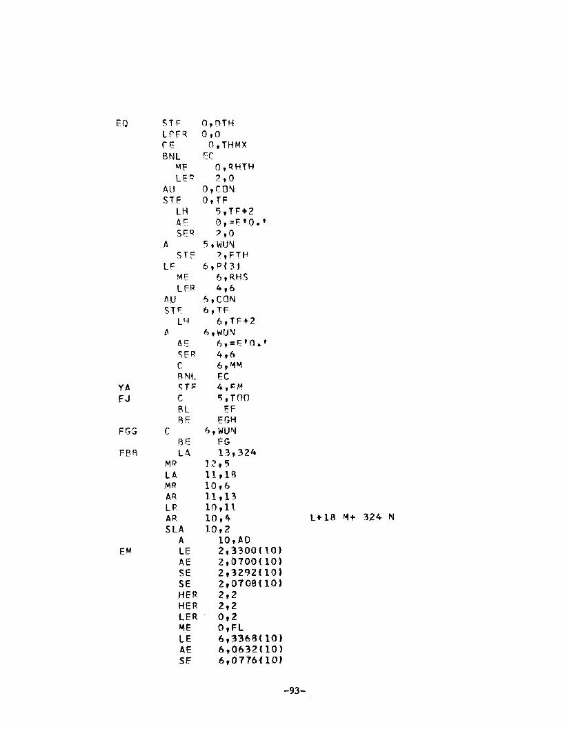
E Q S T F O 9 n T Y L P E S 9 9 0 C E OqTHMX BNL 'X
M F O,Rf-ITY L E Q ?,O
A t l 0 , C O Y STF 0 9 T F
LH 5 , T F + 2 P' 09 =E ' 0 . ' S E Q 7 9 0
A 5 , WUhJ
CF 69''(31 S T F 79FTt-I
nvlc 59RHS LEP 4 . 6
P kJ 5tCON STF 6 9 T F
L 'i 6 9 T F + 2 P 4 9 WUY
A' r j ,=E'O. ' t;FR 496 c 6 , Y Y RNL EC
Y b CTF 4 9 F M FJ t 5 9 TOO
R L EF !3E EGH
FGS C f?,,WUY R E FG
?F(S LA 131324 M Q 1 7 9 5 LA 13.18 MR 1096 AS 1 1 9 1 3 L P. ' L O 9 1 1 AR 1 0 . 4 SLA 1092
A 1 0 9 A D E M LE 293'3.00(10)
AE 29O700( LO) SE 2932921 101 SE 2 9 07 08 ( 10 1 HEP 292 HER 2 9 2 LER 0 9 2 YE 0 ,Ft LE 693368t 10) A € 690632(10) Si? 6 9 0 776 l 1 0 )
L+1R Y + 324 N
-93-
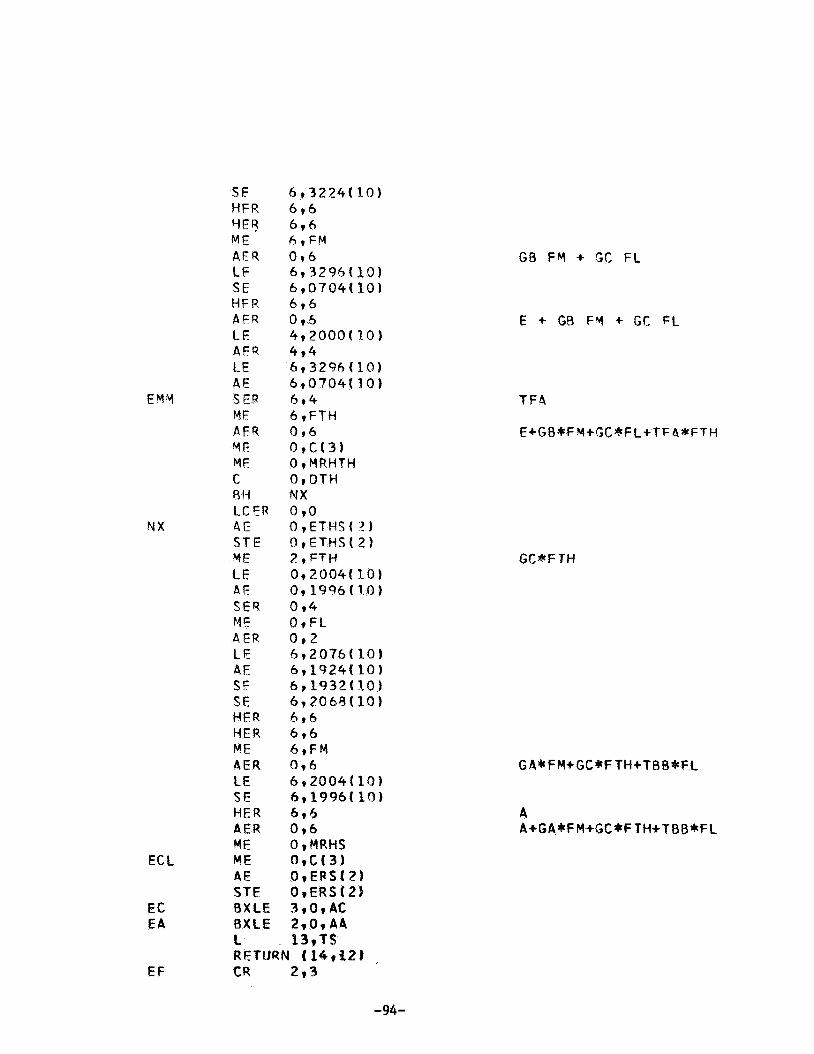
SF HFR YER M E A F R LF SE H F R AFR CF AFQ LE AE
EYsl S EP MF AFQ VF ME C R 1-1 LCER
NX 4E S T E YE LE Ai? S E R MF 4 E R L E AE St SE HFR HER ME 4 E R LE SE H E R AER ME
EC L M E AE STE
EC BXLE EA BXLE
1. RETlJRN 114r921 ,
EF CR 2 r 3
GB FY + GC FL
E + GR Fo4 + GC FL
G C * F T H
GA*FM+GC+FTH+TBR+FC
a A+GA*FM+GC*FTH+TBB*FL
-94-
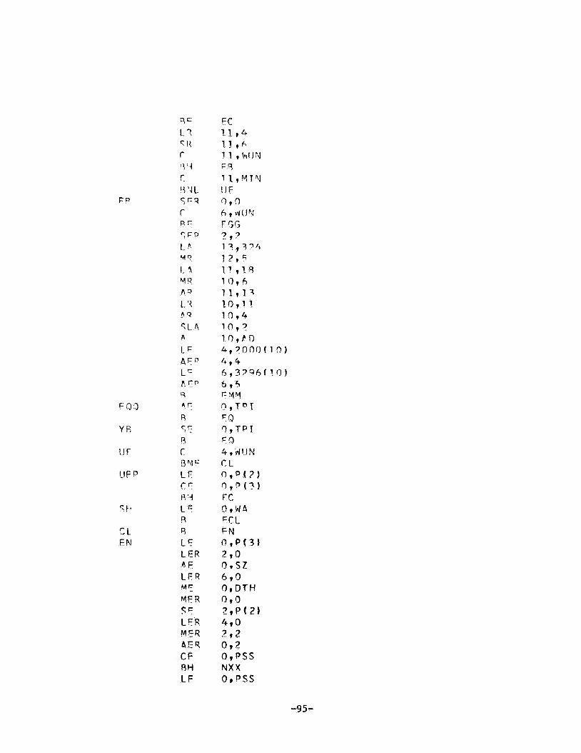
F O
r ..L F N
-95-
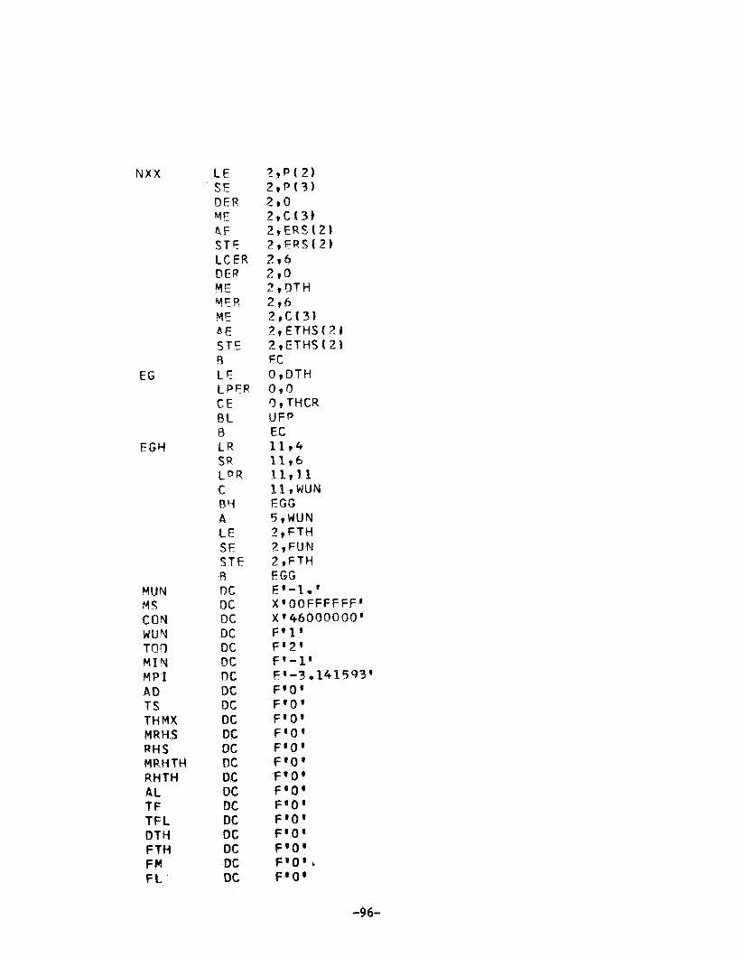
N X X
EG
EGY
MUN MS GUN WUY TQ 0 M I Y MPI AD TS THMX MRHS RHS MRHTH RHTH AL TF TFL DTH F Tii F M F L
L F S E DER F-1 E 4 E STF LCER DER rYE Y E R HF f iF S T E E3 L E t P F R CE BL B L R SR L D R C BY A LE SE S T E R DC DC DC DC OC DC DC DC DC oc DC DC DC OC DC DC DC DC DC DC DC
-96-

-97-
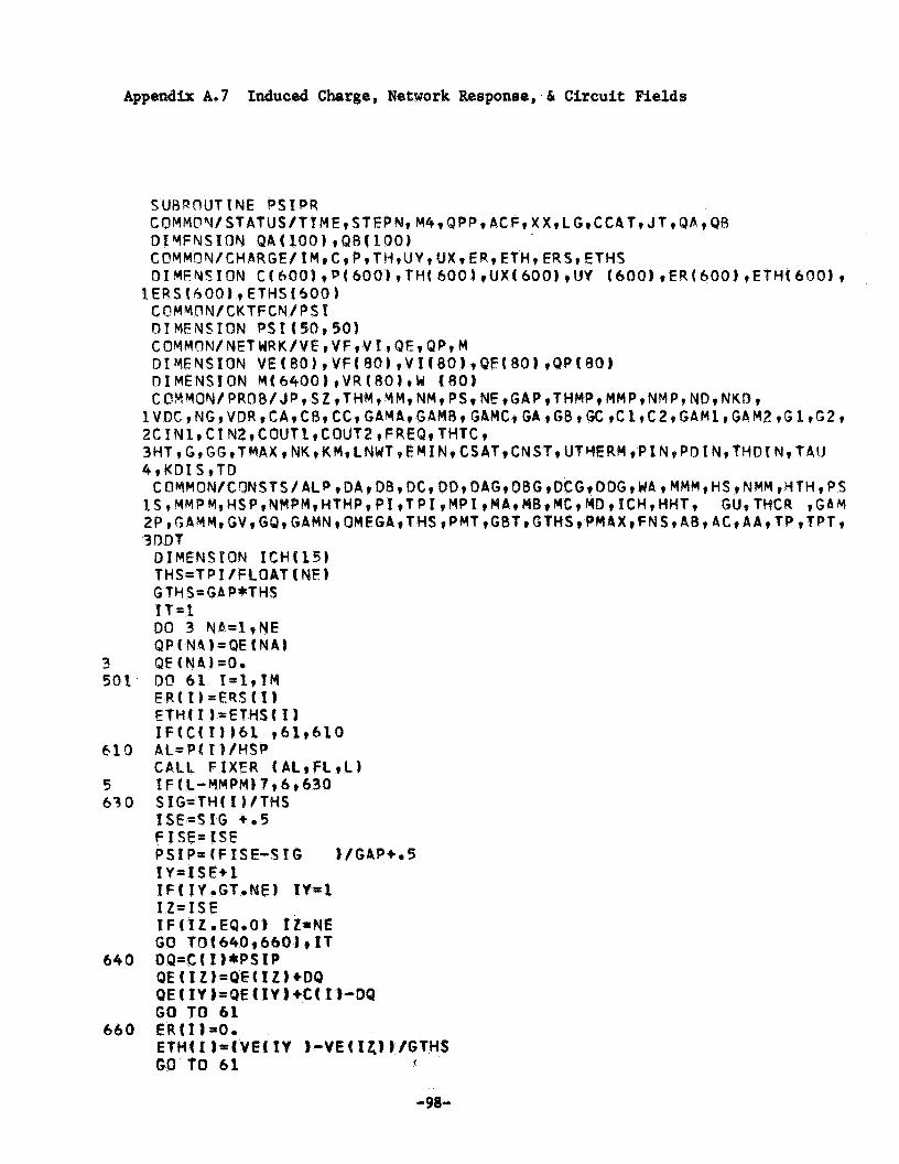
Appendix A.7 Induced Charge, Network Response, & Circuit F ie lds
-98-
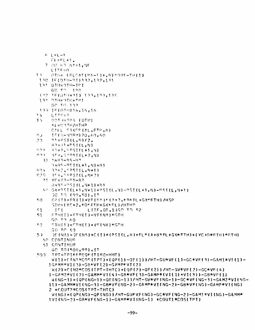
-99-

-1 08-

Appendix A. 7.1
I
L
L
c ClY WCl'J TF Ti;
TK TH
-101-

Appendix A.7.2
-1 02-
Appendix A . 8 Cathode Emission
-103-
-1 04-
-1 05-
Appendix A . 9 Trajectory Calculation
C
11
3
7
-1 06-
-107-

W = C ~ I ~ * l U X ~ I ~ ~ + 2 + U Y ~ I ) $ $ 2 ) dAN(ISF)=WRN1ISFl+W SAN=SAN+C(I) WAT=WbT+W
D(I)=PMT THAIL)=TH( I ) * 5 7 0 2 9 5 7 8
IF(LoFQo1O)GO TQ 20 140 L=L+ I
GO TO 20
20 CONTINUE CM=L J M=J DO 721f=LM,10
311 CA(IJ=Oo DO 39 JsJMp50
GO TO 120012201rMD
132 c ( r i = - ~ l .
30 C K ( J ) = O o
200 CALL PDUMP(UXpUX1TMlv5,UY r U Y (?MI951 2 2 0 PFTURN
END
-1 08-
Appendix A.10 Merge, Collect and Output
-1 09-
-111-
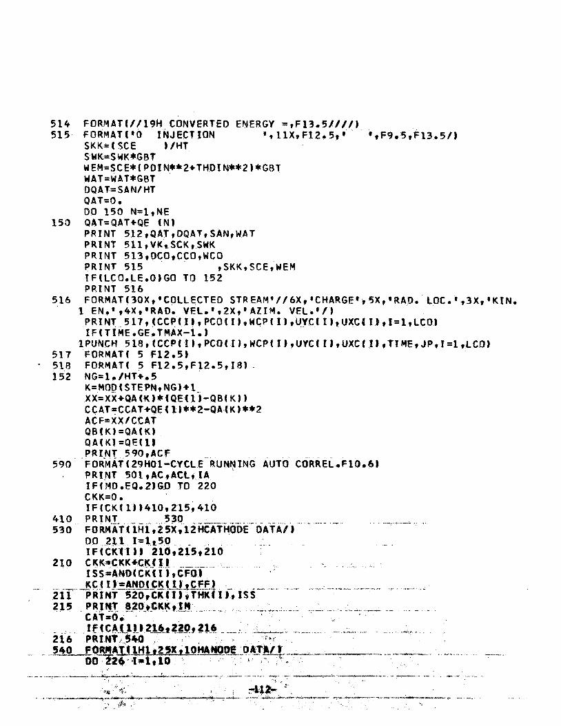
514 FORMATI/ /19H CONVERTED ENERGY =,F13.5/// /) 515 f O R M A T ( * O INJECTION ' r l l X v F 1 2 . 5 , ' 'rF9*5,F13e5/)
SKK= ( SCE 1 /HT S WK=SUK*GBT W E M = S C E ~ ( P D I N * ~ 2 + T H D I N * ~ Z ~ * G ~ T WAT=WAT*GBT DQAT-SAN/HT QATtO 00 150 N=l,NE
P R I N T SiZ,BAT,DQAT,SANvWAT PRINT 511 9 VK,. SCK 9 SWK PRINT 513,DCO,CCO,WCO P R I N T 5 1 5 ,SKK,SCE,WEM IF(LC0oLEoO)GO TO 1 5 2
151) QAT=QAT+QE (N)
PRINT 514 516 FORMAT(3OX,'COtLECTED S T R E A M t / / 6 X t ' C H A R G E ' , 5 X , * ~ ~ ~ o LOCo'r3Xp'KIN.
I. E N o ' 9 4 X t ' R A D o VELoet2X, 'AZIMo VECo'/l PRINT IF 4 J IME eGEo TMAX-1 1
1PUNCH
517, ( C C P t I 8 t PCOI I ) * W C P I I ) 9UYCt I ) r UXCI I 1 , I = l ,LCD)
5 18 9 ICCPI I 1 9 PCD4 ? I 9 WCPI I ) r U Y C I I I t UXC I ? I , T I ME, JP. !=I. 9LCO) 517 FORMAT( 5 F12.5)
- 518 FORMATI 5 f12o5,FlZo5,181. 1 5 2 NG=l./NT+oS
K=MOD f STE PNq NG )+ 1- XXtXX+QA(K)*IQE(l)-QB(K)) C C A T = C C A T + Q E ( 1 ) + * 2 - Q A { K ) * ~ 2 AC F= X X I CCAT QBfK)=QA(K) QAlK?-QEIl) PRINT 590,ACF
PRINT SOL ~ACIACL, IA 590 -FORMAt(29HOl-CYCLE"RUNNING AUTO 60RREL.Fl0061
IF(HDeEQo21GD TO 220 CKK=O I F t C K I 1) )41012159410

? ? 5
? ? 5 2 2 0 ?)?Cl
203 p.30 1 2 2 739
77 75 2 ? ?
-113-

Appendix A. 10.1
T I T L E 'REALIXYTEGER FUNCTION ANDII,Jl* ENTRY AND R A L R 1 5 9 0 U S I N G * ~ 1 5
L 14rOIL) L 0 , 0 1 1 4 ) L 1 4 , 4 ( 1 1 N 0 , 0 1 1 4 ) ST O l T
LF O v T RFTURN ( 1 4 )
AN9 S A V E ( 1 4 . 5 1
T 13s IF E Y D
-114-
Appendix A. 10.2
-1 15-

Appendix A . l l Fourier Analysis
-1 16-
*57,29577?5
211 0 E * 9 4 X 9 ' A NGC E ' / 1 1 I 2 FORMIT4 I 1 4 9 F 8 0 3 9 F 9 e 2,1PE13o4qOPf9e2# 22 23 FORMAft'l'/(I15~2FlO.48 1
f ORMAT 4 31X q 1 PE13.49 OPF90 2 8
END
-117-
FUNCTTON ATAN3(AvB) I F ( A a F Q a O . ~ A N D . R . E Q a O a ~ G O TO 1 ATAN3=6TANZ(A,Bl
2 RETURN
RETURN END
1 ATAV\19=0a
-1 18-

REPORT DISTRIBUTION LIST FOR CONTRACT NO, NAS3-9710
National Aeronautics and Space Administration Headquarters Washington, D. C. 20546 Attention: SA/L. Jaffe - 1 cy.
SAC/A. M. G. Andrus - 10 cys. National Aeronautics and Space Administration Lewis Research Center 21000 Brookpark Road Cleveland, Ohio 44135 Attention: C. C. Conger, MS 54-1 - 1 cy.
R. E. Alexovich, MS 54-3 - 1 cy, Dr. H. G. Kosmahl, MS 54-3 - 1 cy. Technology Utilization Office, MS 3-19 - I cy. Agena & Support Procurement Sec., MS 500-110 - 1 cy, Library, MS 60-3 - 2 cys. Report Control Office, MS 5-5 - 1 cy. N. T. Musial, MS 501-3 - 1 cy. G. J. Chomos, MS 54-3 - 5 cys.
Communication Systems, Inc. 5817 Columbia Pike Falls Church, Virginia 22046 Attention: J. Bisaga - 1 cy. Rand Corporation 1700 Main Street Santa Monica, California 90404 Attention: Dr. J. Holt - 1 cy. NASA Electronics Research Center 575 Technology Square Cambridge, Massachusetts 02139 Attention: E/Dr, L. Van Atta - 1 cy.
EM/C. Veronda - 1 cy. Library - 1 cy.
National Aeronautics and Space Administration George C. Marshall Space Flight Center Huntsville, Alabama 35812 Attention: RASTR-A/E. C. Hamilton - 1 cy.
Library - 1 cy. National Aeronautics and Space Administration Goddard Space Flight Center Greenbelt, Maryland 20771 Attention: 733/R. Pickard - 1 cy.
Library - 1 cy.
-119-

National Aeronautics and Space Administration Ames Research Center Moffett Field, California 94035 Attention: OART-MAO/E. Van Vleck, MS 202-6 - 1 cy.
Library - 1 cy.
National Aeronautics and Space Administration Langley Research Center Langley Station Hampton, Virginia 23365 Attention: B. Kendall, MS 173 - 1 cy.
Library, MS 185 - 1 cy. National Aeronautics and Space Administration Manned Spacecraft Center Houston, Texas 77001 Attention: Library - 1 cy.
Jet Propulsion Laboratory 4800 Oak Grove Drive Pasadena, California 91103 Attention: L. Derr - 1 cy.
Library - 1 cy.
National Aeronautics and Space Administration Scientific and Technical Information Facility P. 0. Box 5700 Bethesda, Maryland Attention: NASA Representative - 3 cys.
Radio Corporation of America Astro-Electronics Division Princeton, New Jersey 08540 Attention: R. B. Marstin - 1 cy.
TRW Systems One Space Park Redondo Beach, California 90278 Attention: W. A. Finley/Space Vehicle Division - 1 cy.
General Dynamics Corporation Convair Di7iision P. 0. Box 1128 San Diego, California 92112 Attention: F. J. Dore/Advanced Programs Laboratory - 1 cy. Hughes Airdraft Company Space Systems Division 1194 West Jefferson Boulevard Culver City, California 90230 Attention: H. A. Rosen/Satellite Systems Laboratory - 1 cy.
-120-

General Electric Company Missile and Space Division Valley Forge Space Technology Center P. 0. Box 8555 Philadelphia, Pennsylvania 19101 Attention: H. Collins - 1 cy.
P. Nadler - 1 cy.
Federal Communications Commission 521 Twelfth Street Washington, D. C. 20554 Attention: H. Fine - 1 cy.
U. S. Information Agency 25 M. Street S.W. Washington, D. C. 20547 Attention: IBS/EF/G. Jacobs - 1 cy.
General Electric Company Tube Department Microwave Tube Business Section Schenectady, New York Attention: R. Dehn - 1 cy.
Litton Industries Electron Tube Division 960 Industrial Road San Carlos, California 94070 Attention: Dr. G. Pokorney - 1 cy.
J. Orr - 1 cy. S-F-D Laboratories, Inc. 800 Rahway Avenue Union, New Jersey 07083 Attention: Dr. G. Farney - 1 cy. Hughes Aircraft Company Electron Dynamics Division P. 0. Box 2999 Torrance, California 90509 Attention: Dr. J. Mendel - 1 cy. Watkins Johnson Co. 333 Hillview Avenue Palo Alto, California 94304 Attention: Dr. D. Watkins - 1 cy. Varian Associates 611 Hansen Way Palo Alto, Californlla 94303 Attention: F. Melzer - 1 cy.
RCA Industrial Tube Division Lancaster, Pennsylvania Attention: W. P. Bennett - 1 cy.
-121-