analysis of the power conversion efficiency on energy...
TRANSCRIPT

1
Analysis of the Power Conversion Efficiency on Energy
Scavenging Interface Circuits
Kevin Petsch, Robert Balma, Tolga Kaya
Central Michigan University
Mt Pleasant, MI 48858
email: {petsc1k, balma1rw, kaya2t}@cmich.edu
Abstract
In this paper, we report a comprehensive survey on power conversion efficiency of
energy scavenging interface circuits. A realistic energy input model for vibrational
systems was used and theoretical analysis provided. The realistic energy provided by
energy scavenging system can be modeled with a sinusoidal current source in parallel
with a capacitor and resistor whereas the magnitude and sinusoidal frequency of the
current relate to vibrational magnitude and vibration frequency, respectively. We
analyzed and designed different interface circuits used in the energy scavenging system
which includes a full-wave, voltage multiplier, and half-wave rectifier. Simulations were
performed using IBM’s 130 nm CMOS technology under the Cadence design platform.
Each interface circuit was characterized to demonstrate their output power and efficiency.
Optimizations of individual topologies were performed to yield maximum efficiency for
different loads. We believe this comprehensive analysis will provide a good starting point
to circuit designers in the energy scavenging society.
1. Introduction
The need for compact, portable, long-lasting, wireless technology is increasing with time
for many applications such as wireless sensor networks, biomedical implants, or other
circuit systems requiring microwatts of power1. These parameters are the force
compelling technologies to develop smaller, more efficient designs. The reduction in size
and power consumption of these technologies creates a unique opportunity to develop
ultra-low power systems capable of batteryless function. This function is essential in the
development of self-sustaining wireless technologies. Applications of this self-sustaining
technology include ultra-low power systems such as micro-sensor networks and
biomedical implants where battery replacement is extremely difficult or impossible2.
Ambient energy is available in many different forms which provide an excellent source
of power with absolutely no cost. Sources of ambient energy are geothermal/ thermal
changes, vibration, solar, and wind power3-5. Sources of energy to power electronics can
also come from unexpected places such as the friction from clothes rubbing together or
the vibration in the sole of a shoe when walking.
Self-sustaining wireless and green technologies are the driving force for energy
scavenging systems. Energy harvesting for low-power circuits is possible using many
different techniques. The most effective method in powering wireless micro-sensor
networks is through vibrational energy scavenging. Efficient vibrational energy
transducer methods include electrostatic (capacitive) and piezoelectric energy
scavenging6. Other approaches such as electromagnetic transducers are options as well
2.
These methods, however, rely on forms of ambient energy that may not occur in large
Proceedings of the 2011 ASEE NC & IL/IN Section Conference Copyright © 2011, American Society for Engineering Education

2
enough magnitude or frequency for some applications. An example of such situation
might include a solar powered interface circuit in an enclosed indoor environment. The
same applies for any energy scavenging method but, vibrational energy harvesting is
especially attractive because the resonant frequency of the circuit can be manipulated
using adaptive circuitry7.
Understanding the different approaches in energy scavenging methods is essential to
create efficient, optimized systems capable of self-sustainability. Not only is it possible to
energize ultra-low power circuits but, with enough research, larger devices will become
self-powered as well. For low-vibration commercial settings, the most common method
for energy harvesting uses piezoelectric materials8.
Several interface methods are developed in order to extract power from the piezoelectric
material which includes bias-flip2, full-bridge, and voltage doubler rectifiers
9. A Realistic
energy model for vibrational energy can be realized when piezoelectric materials are
implemented using a sinusoidal current source in parallel with a capacitor and resistor
whereas the magnitude and sinusoidal frequency of the current relate to vibrational
magnitude and vibration frequency, respectively2,10
.
We theoretically studied and simulated different interface circuits used in the energy
scavenging system which includes a full-wave, doubler, and half-wave rectifier. We
performed the simulations of each interface circuit using the Cadence design platform.
Each circuit was simulated in order to characterize its properties and exhibit its power
and efficiency. The interface circuits were then analyzed to optimize performance and
provide the most scavenged ambient power. We provide an analysis of different load
resistances to demonstrate a maximum efficiency. We believe this analysis of common
interface circuits will benefit circuit designers seeking to design new energy harvesting
systems.
2. Equivalent circuit of energy harvester
A common source of ambient energy is vibration and an effective method of extracting
this energy is using piezoelectric materials. Vibrational energy can vary in both
magnitude and frequency. Energy harvesters have an intrinsic resonance frequency in
which maximum power is obtained from the ambient source. This poses a challenge
because vibrations are uncontrollable and the resonant frequency is rarely created.
Ambient energy from vibration is unique because it can be modeled using mechanical
mass spring system when harvested by piezoelectric materials.
A Realistic energy model for vibrational energy can be realized using a sinusoidal current
source in parallel with a capacitor and resistor whereas the magnitude and sinusoidal
frequency of the current relate to vibrational magnitude and vibration frequency,
respectively2, 10
. This model is particularly useful for running computer simulations in a
software program such as Cadence.
Vibrations can be measured in any environment and converted into this equivalent
circuit. This configuration can then be used in combination as a power source for
different interface circuits in order to extract the ambient energy.

3
Figure 1: Equivalent circuit of piezoelectric energy signal.
3. Common Interface Circuits
The full-bridge, half-wave, and voltage multiplier rectifier circuits were constructed using
the Cadence design platform. The power source of each interface circuit is the
piezoelectric model as shown above. This source was used to analyze the characteristics
of each rectifier circuit. In order to properly analyze each interface method, the process of
calculating power and efficiency is necessary. The values of the load current, internal and
source capacitors affect the resonant frequency the circuit.
We designed the piezoelectric model to have a frequency value similar to what a
commercial setting might demonstrate. This allowed us to choose capacitances
accordingly. Once the values were chosen, the output voltage was simulated and
compared to the input voltage. Using parametric analysis, an efficient load current was
realized and provided a maximum output voltage.
Once an optimum load current was found, the efficiency of each circuit was then
calculated. Efficiency, in this case, is the ratio of the output voltage and the input voltage
supplied from the piezoelectric model. This value is calculated by taking the ratio of the
average of the output voltage over the average of the input voltage during a specific
interval of time. Once the maximum efficiency was found, an analysis of different
efficiencies for different load currents is provided.
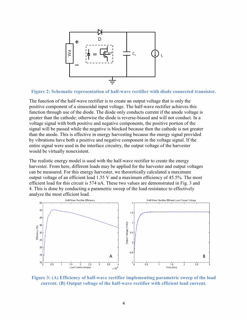
3.1 Half-Wave Rectifier
The first interface circuit we theoretically studied and simulated was the half-wave
rectifier. Using IBM’s 130 nm technology, diodes were created by connecting the gate
and drain terminals of the transistors. Then, using these diode elements and capacitors, a
half-wave rectifier was created. The source capacitor is necessary because this is the
constant voltage source the harvester will provide once the rectifier charges it. Without
the source capacitor, a DC voltage source is not replicated and is not useful.
4
Figure 2: Schematic representation of half-wave rectifier with diode connected transistor.
The function of the half-wave rectifier is to create an output voltage that is only the
positive component of a sinusoidal input voltage. The half-wave rectifier achieves this
function through use of the diode. The diode only conducts current if the anode voltage is
greater than the cathode; otherwise the diode is reverse-biased and will not conduct. In a
voltage signal with both positive and negative components, the positive portion of the
signal will be passed while the negative is blocked because then the cathode is not greater
than the anode. This is effective in energy harvesting because the energy signal provided
by vibrations have both a positive and negative component in the voltage signal. If the
entire signal were used in the interface circuitry, the output voltage of the harvester
would be virtually nonexistent.
The realistic energy model is used with the half-wave rectifier to create the energy
harvester. From here, different loads may be applied for the harvester and output voltages
can be measured. For this energy harvester, we theoretically calculated a maximum
output voltage of an efficient load 1.55 V and a maximum efficiency of 45.5%. The most
efficient load for this circuit is 574 nA. These two values are demonstrated in Fig. 3 and
4. This is done by conducting a parametric sweep of the load resistance to effectively
analyze the most efficient load.
Figure 3: (A) Efficiency of half-wave rectifier implementing parametric sweep of the load
current. (B) Output voltage of the half-wave rectifier with efficient load current.

5
The efficiencies of these circuits are measured by taking the output voltage over the input
voltage and are calculated using the following equation in the Cadence Design Platform
where Vout is the voltage at the output node and Vin is the input voltage from the
piezoelectric model:
���������� �� �� ∗ ����� ∗ �� � , 23�
This equation yields the efficiency of the circuit by taking the average of the signals during a
clipping period from two to three seconds. This equation produces the efficiency graph when a
parametric sweep of the load current is performed.
3.2 Voltage Multiplier
The voltage multiplier achieves the same function as the half-wave rectifier in the sense
that only the positive portion of the ambient signal is used. A multiplier increases the
output voltage achieved by the energy harvester but at the cost of efficiency. The
multiplier achieves its function because the first capacitor and diode act just as a half-
wave rectifier during the positive portion of the input signal. When the input signal
becomes negative, the first diode is then reverse biased and the second is forward
allowing the first capacitor to aid in charging the storage capacitor creating a voltage
equal to double the input. The actual voltage created is not equal to exactly double
because the voltage drop across the diodes need to be accounted for. The most simple
voltage multiplier is the voltage doubler, shown below.
Figure 4: Schematic representation of voltage doubler.
The voltage doubler achieved a peak efficiency of 58% with an output voltage of 1.9 V. The load
current which provided the greatest efficiency is 574 nA. These values are demonstrated in Fig.
5.
6
Figure 5: (A) Efficiency of the X2 voltage multiplier implementing parametric sweep of the
load current. (B) Output voltage of the X2 voltage multiplier with efficient load current.
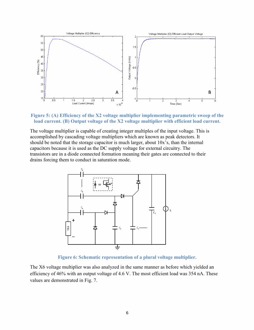
The voltage multiplier is capable of creating integer multiples of the input voltage. This is
accomplished by cascading voltage multipliers which are known as peak detectors. It
should be noted that the storage capacitor is much larger, about 10x’s, than the internal
capacitors because it is used as the DC supply voltage for external circuitry. The
transistors are in a diode connected formation meaning their gates are connected to their
drains forcing them to conduct in saturation mode.
Figure 6: Schematic representation of a plural voltage multiplier.
The X6 voltage multiplier was also analyzed in the same manner as before which yielded an
efficiency of 46% with an output voltage of 4.6 V. The most efficient load was 354 nA. These
values are demonstrated in Fig. 7.

7
Figure 7: (A) Efficiency of thr X6 voltage multiplier implementing parametric sweep of the
load current. (B) Output voltage of the X6 voltage multiplier with efficient load current.
The X10 voltage multiplier was also analyzed in the same manner as before which yielded an
efficiency of 42.2% and output voltage of 6.9 V. The most efficient load was 218 nA. These
values are demonstrated in Fig. 8.
Figure 8: (A) Efficiency of the X10 voltage multiplier implementing parametric sweep of
the load current. (B) Output voltage of the X10 voltage multiplier with efficient load
current.
3.3 Full-Wave
The full-wave rectifier is unique because its formation allows the negative portion of the
input signal to follow the same current path as when it does during the positive input
signal. The full-bridge rectifier consists of diode pairs connected in series. There are two
pairs but only one pair is on per half cycle of the sinusoidal input signal. The diode pairs
are connected in such a way that the current from the source flows through the load in the
same direction during each half cycle. There exists a ripple voltage if a storage capacitor
is not implemented. This storage capacitor essentially removes the ripple allowing for a
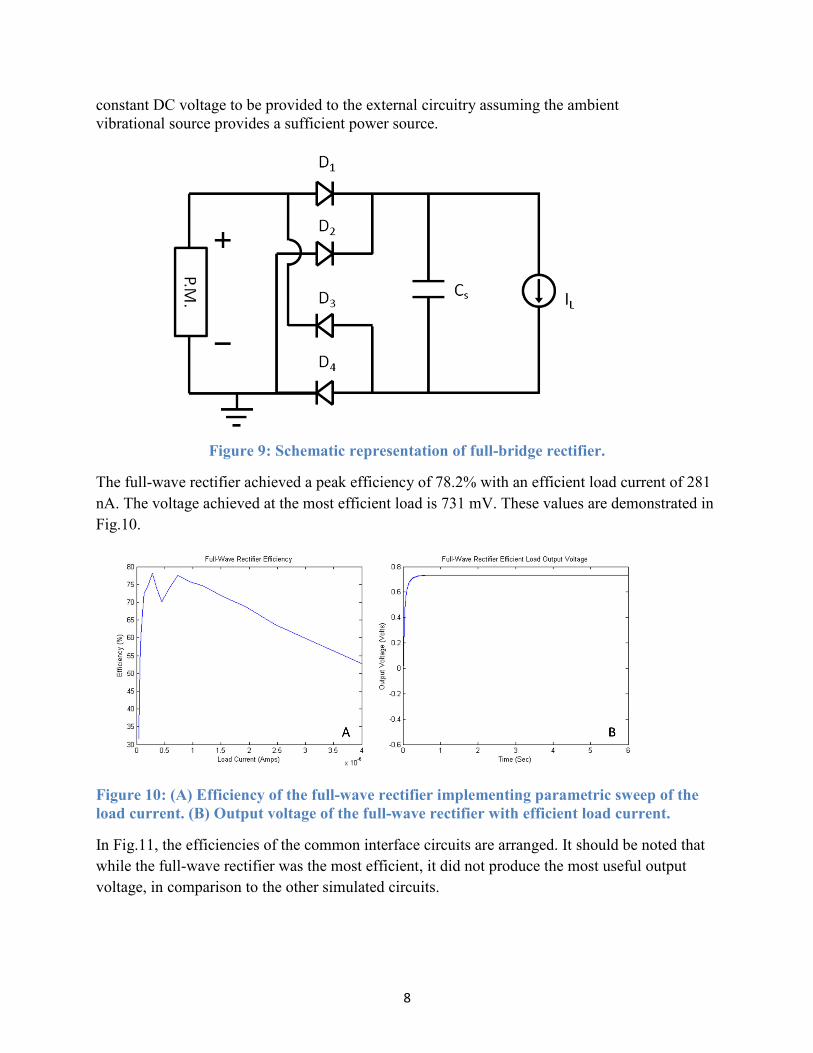
8
constant DC voltage to be provided to the external circuitry assuming the ambient
vibrational source provides a sufficient power source.
Figure 9: Schematic representation of full-bridge rectifier.
The full-wave rectifier achieved a peak efficiency of 78.2% with an efficient load current of 281
nA. The voltage achieved at the most efficient load is 731 mV. These values are demonstrated in
Fig.10.
Figure 10: (A) Efficiency of the full-wave rectifier implementing parametric sweep of the
load current. (B) Output voltage of the full-wave rectifier with efficient load current.
In Fig.11, the efficiencies of the common interface circuits are arranged. It should be noted that
while the full-wave rectifier was the most efficient, it did not produce the most useful output
voltage, in comparison to the other simulated circuits.

9
Figure 11: Maximum efficiencies of the common interface circuits at most efficient load
current.
4. Applications
Applications of systems that only require microwatts of power are perfect candidates for
energy harvesting circuits. Specific applications that require ultra low power include
wireless sensor micro-sensor networks 11, tire-pressure sensor systems
12, and implantable
medical electronics2.
The application of IBM’s 130nm CMOS technology is best suited for extracting ambient
energies on scales less than one volt. This is because the transistor has a smaller channel
length and can function with much lower threshold voltages. This property makes this
technology a perfect candidate for systems requiring microwatts of power.
Systems that could take advantage of the efficiency of this technology might include
wireless micro-sensor networks. This becomes even more intriguing if the devices to be
powered are fabricated using IBM’s technology. This would improve the minimum
voltages required to power micro-devices. Wireless micro-sensor networks for process
monitoring would be an ideal candidate for implementing these piezoelectric energy
harvesters. Lead zirconate titanate (PZT) is an effective ceramic in piezoelectric energy
harvesting applications and is best suited for low-level vibrations6. PZT is most effective
with low-level vibrations because the material is fragile with relatively high vibration
amplitudes and frequencies.

10
5. Conclusions
Based on the values derived from the simulations using IBM’s 130nm CMOS
technology, the multipliers with the highest efficiency produced the best results in terms
of extracting the most ambient vibrational energy. The piezoelectric energy model’s
values were chosen solely based on values one might encounter in a low-level vibrational
facility. Without adding any external circuitry, the power extracted ranges from 10 nano
to 20 microwatts of power. In comparison to previous methods which produced power on
the order of a few hundred micro watts, the values achieved here are much lower. This is
due to the fact that the input signals in other methods are much higher than values used in
these simulations. This does not mean that other methods are more efficient. IBM’s
130nm CMOS technology is much smaller than technology from other methods. This
enabled the energy harvester interface circuits to yield a higher efficiency.
This technology for energy scavenging is useful in exceptionally low vibration systems.
Other methods have larger technology which would require larger input signals from the
piezoelectric model. These values include a larger amplitude and frequency. IBM’s
technology sidesteps this in creating smaller, more efficient technologies. The channel
length of the transistors used in these simulations is 130 nm where previous methods
have much longer channel lengths. The smaller technology created by IBM provides an
opportunity to create smaller, more efficient devices which takes technology one step
closer to complete self-sufficiency and batteryless applications.
6. Acknowledgements
A special thanks to Professor Kumar Yelamarthi for his support and effort in setting up
the necessary software and technology libraries for use with the Cadence design and
simulation programs. His help made theoretical analysis and simulation of energy
harvesting interface circuits possible and a great success.
[1] Cao, Y., Steigerwald, M. L., Nuckolls, C. and Guo, X. (2010). “Current Trends in Shrinking the
Channel Length of Organic Transistors Down to the Nanoscale,” Advanced Materials, 22: 20–32.
[2] Ramadass, K. Yogesh. “An Efficient Piezoelectric Energy Harvesting Interface Circuit Using a
Bias-Flip Rectifier and Shared Inductor,” IEEE Journal of Solid-State Circuits, vol. 45, 189.
[3] Yildiz, Faruk. “Potential Ambient Energy-Harvesting Sources and Techniques”, The Journal of
Technology Studies, 40.
[4] Zhi Ang Eu, Hwee-Pink Tan, Winston K.G. Seah, “Opportunistic routing in wireless sensor
networks powered by ambient energy harvesting”, Computer Networks, Volume 54, Issue 17, 3
December 2010, Pages 2943-2966.

11
[5] Sudevalayam, S.; Kulkarni, P., "Energy Harvesting Sensor Nodes: Survey and Implications,"
Communications Surveys & Tutorials, IEEE, vol.PP, no.99, pp.1-19.
[6] Shu, Y.C., “Analysis of Power Output for Piezoelectric Energy Harvesting Systems”, The Journal
of Smart Materials and Structures, 1499.
[7] Ottman, G.K.; Hofmann, H.F.; Bhatt, A.C.; Lesieutre, G.A.; , "Adaptive piezoelectric energy
harvesting circuit for wireless remote power supply," Power Electronics, IEEE Transactions on ,
vol.17, no.5, pp. 669- 676, Sep 2002.
[8] Anton, R. Steven. “A Review of Power Harvesting Using Piezoelectric Materials,” The Journal of
Materials and Structures, vol. 16, R1-R21.
[9] Priya, S., Inman, D. Energy Harvesting Technologies, New York: Springer Science + Business
Media, 2009.
[10] Zhao, Zhou. “Piezoelectric Micro-Power Generation to Charge Supercapacitor With Optimized
Duty Cycle,” Journal of Intelligent Material Systems and Structures, Vol. 21, July 2010.
[11] Benton H. Calhoun, Denis C. Daly, Naveen Verma, Daniel F. Finchelstein, David D. Wentzloff,
Alice Wang, Seong-Hwan Cho, and Anantha P. Chandrakasan. 2005. Design Considerations for
Ultra-Low Energy Wireless Microsensor Nodes. IEEE Trans. Comput. 54, 6 (June 2005), 727-
740.
[12] Seeman, M.D.; Sanders, S.R.; Rabaey, J.M.; "An Ultra-Low-Power Power Management IC for
Wireless Sensor Nodes," Custom Integrated Circuits Conference, 2007. CICC '07. IEEE, vol., no.,
pp.567-570, 16-19 Sept. 2007.