analysis of statcom for voltage dip...
TRANSCRIPT
Analysis of STATCOM for
Voltage Dip Mitigation
Cai Rong
Thesis for the Degree of Master of Science, December 2004
Department of Electric Power Engineering Chalmers University of technology Göteborg, Sweden ISSN 1401-6184 M.Sc. No. 111E

Titel Analys of STATCOM för att mildra spänningsdippar Title in english Analysis of STATCOM for voltage dip mitigation Författare/Author Cai Rong Utgivare/Publisher Chalmers Tekniska Högskola Institutionen för elteknik 412 96 Göteborg, Sverige ISSN 1401-6184 Examensarbete/M.Sc. Thesis No. 111E Ämne/Subject Power systems/power electronics Examinator/Examiner Ambra Sannino Datum/Date 2004-12-03 Tryckt av/Printed by Chalmers tekniska högskola 412 96 GÖTEBORG

Abstract Static Synchronous Compensator (STATCOM) is a Custom Power Device based on a Voltage Source Converter (VSC) shunt connected to the grid. By injecting a controllable current, it can improve the quality of the load current, e.g. compensating harmonic currents or fluctuating currents. However, a STATCOM can also mitigate voltage dip by injecting current at the point of connection with the grid. This thesis focuses on the STATCOM for mitigating voltage dips. First, characteristics of the STATCOM for mitigating voltage dips are studied, such as the required shunt compensation current, injected active and reactive power for given voltage dip magnitude. This is done for different grid impedances and load characteristics (i.e. constant impedance load and constant current load). The results of this study show that the shunt compensation current, injected active and reactive power decrease as the impedance, which is the source impedance in parallel with the load impedance, increases. It also shows that reactive power is the main requirement for voltage dip compensation by STATCOM. All results are verified in MATLAB and simulated in PSCAD/EMTDC. Then, a Dual Vector Controller of the STATCOM, incorporating a vector voltage controller (outer loop) and a vector current controller (inner loop), is designed for mitigating the voltage dip and tested in simulation. The simulation models are implemented by the PSCAD/EMTDC. Three controller simulation models are reported in this thesis, which are Vector Voltage Controller with a simplified VSC, Dual Vector Controller with a simplified VSC and Dual Vector Controller with a real VSC. Three controllable current sources and three controllable voltage sources are used to represent the STATCOM and the VSC in the first two models, respectively. The Pulse-Width Modulation (PWM) strategy is implemented in the third model. The vectors are implemented by using the Clarke and Park transformations to realize the controller system. In order to obtain the phase and frequency information of the grid voltage, Phase-Locked Loop is used in the controller system. The voltage dip can be mitigated in 5 ms by using the reactive power control in the vector voltage controller and the deadbeat gain in the vector current controller for the second simulation model. The third simulation model is verified both in 400 V system and 10 kV system. When applying the STATCOM in a 10 kV system, the STATCOM configuration must be changed by replacing the L-filter with LCL-filter. It is shown that the STATCOM with LCL-filter has robust performance, but the reactive current requirements are very high. Keywords: Static Synchronous Compensator (STATCOM), Voltage Source Converter (VSC), voltage dip, shunt compensation, dual vector controller
- i -

Acknowledgements This work has been carried out at Department of Electric Power Engineering, Chalmers University of Technology in Göteborg. I would like to special thanks my supervisor Associate Professor Ambra Sannino and Massimo Bongiorno for their support and encouragement during the work. Thanks for their patient discussions in each meeting. I also thank Daniel Nilsson for his help at the beginning of the work. I wish to thank my classmates Einar Pálmi Einarsson, Bengt-Olof Wickbom and Frantisek Kinces for their discussions and jokes during the work. I would like to thank my family for their love and support throughout the years.
- ii -
Table of Contents
Abstract
Acknowledgements
Table of Contents
Chapter 1 Introduction……………………………………………..1 1.1 Background…………………………………………………………1 1.2 Objective……………………………………………………………1 1.3 Thesis outline……………………………………………………….1
Chapter 2 Voltage Dips and Mitigation……………………………3 2.1 Characteristic of voltage dips………………………………………3 2.2 Voltage dip classification…………………………………………...6 2.3 Voltage dip mitigation……………………………………………..7 2.3.1 Motor-generator sets………………………………………7 2.3.2 Transformer-based solutions………………………………8
2.3.3 Power-electronics based solutions………………………...9
Chapter 3 Shunt Compensator for Mitigating Voltage Dips……13 3.1 Structure of Shunt Compensator.…………………………………13 3.2 Theoretical analysis of shunt compensation...……………………..15 3.3 Characteristics of shunt compensation…………………………….19 3.3.1 Different load characteristics……………………………..19 3.3.2 Variation of the load power factor………………………22 3.3.3 Variation of source impedance…………………………...24 3.3.4 Real power system……………………………………….26 3.4 Simulation…………………………………………………………32 3.4.1 Simulation circuit………………………………………...32 3.4.2 Simulation results………………………………………...33 3.5 Conclusions………………………………………………………..36 .
Chapter 4 Dual Vector Controller………………………………...37 4.1 Three-phase Voltage Source Converter.……..…………………….38 4.1.1 VSC scheme……………………………………………...38 4.1.2 Voltage modulation………………………………………39 4.1.3 Pulse Width Modulation (PWM)…………………………42
- iii -
4.2 Vector current controller…………………………………………..43 4.2.1 Derivation of the PI-controller…………………………...44 4.2.2 Step response……………………………………………..49 4.2.3 Controller improvement………………………………….52 4.3 Vector voltage controller…………………………………………..57 4.3.1 Operation principle……………………………………….58 4.3.2 Simulation………………………………………………..60 4.4 Dual Vector Controller…………………………………………….65 4.4.1 Step response……………………………………………..65 4.4.2 Simulation (PSCAD/EMTDC)…………………………...69 4.5 Conclusions………………………………………………………..79
Chapter 5 400 V System Simulation………………………….…...81 5.1 Simulation model………………………………………………….81 5.2 Step response………………………………………………………82 5.3 Simulation results………………………………………………….84 5.4 Conclusions………………………………………………………..91
Chapter 6 Realistic Power System Simulation…………………...92 6.1 Power system model and simulation model……………………….92 6.2 Different filter configuration………………………………………94 6.3 Variation of system parameters……………………………………96 6.4 Conclusions………………………………………………………107
Chapter 7 Conclusions…………………………………………...108
References……………………………………………………………..110
Appendix A Transformations for The Three-phase System……...112
Appendix B Phase-locked Loop……………………………………115
Appendix C Per Unit Definition……………………………………116
- iv -
Chapter 1 Introduction
- 1 -
Chapter 1
Introduction 1.1 Background Nowadays, more and more power electronics equipment, so-called “sensitive equipment”, are used in the industrial process to attain high automatic ability. Susceptibility of these end-user devices draws attention of both end customers and suppliers to the questions of power quality. Especially, short duration power disturbances, e.g. voltage dips, swells and short interruptions, which can bring substantial financial losses to the end customer. Voltage dips are the most common disturbances encountered. The concept of custom power devices is introduced since some years to improve the power quality in industrial plants. Several different custom power devices have been proposed, many of which are based on the Voltage Source Converter (VSC), e.g. Dynamic Voltage Restorer (DVR) and Static Synchronous Compensator (STATCOM) etc. With a DVR installed in series or a STATCOM connected in shunt with the critical load, the line voltage can be restored to its nominal value within the response time of a few milliseconds, thus avoiding any power disturbances to the load. The STATCOM have a function of compensating reactive power, absorbing the harmonic and compensating the voltage dip. This thesis focuses on the function of compensating voltage dip. 1.2 Objective The STATCOM for mitigating voltage dips is studied in this thesis. First the characteristics of the STATCOM in the dip mitigation are studied, such as the variation of the shunt compensation current, injected active and reactive power with respect to the voltage dip magnitude. Then a controller algorithm for voltage dip mitigation with STATCOM is designed and tested via the simulation. The simulations in thesis are based on the Matlab/Simulink and PSCAD/EMTDC. 1.3 Thesis outline This thesis is composed of this introductory chapter, six other chapters and Appendix arranged as below: Chapter 2 briefly introduces the characteristic, classification of the voltage dip. Several voltage dip mitigation devices also are introduced in this chapter.
Chapter 1 Introduction
- 2 -
Chapter 3 studies the characteristic of the STATCOM for mitigating voltage dip, such as the variation of the shunt compensation current, injected active and reactive power with respect to the voltage dip magnitude. The equations used to calculate the shunt compensation currents for different load characteristics are derived and verified by simulation in PSCAD/EMTDC. Chapter 4 describes the design of a dual vector controller of the STATCOM for mitigating voltage dip. The results of the step responses in Matlab/Simulink and simulation in PSCAD/EMTDC are presented in this chapter. Chapter 5 shows the simulation results of the 400V system simulation circuit with a real converter model. Chapter 6 gives the simulation results of a realistic power system simulation circuit with a real converter model. In Appendix, the Park Transformation and Phase-Locked Loop (PLL), which are the useful tools used in the controller design, are described. The per unit definition is also introduced in Appendix.
Chapter 2 Voltage Dips and Mitigation
Chapter 2
Voltage Dips and Mitigation Voltage dips are momentary (i.e. 0.5-30 cycles) decreases in the rms voltage magnitude, caused by short-duration increases of the current. The most common causes of overcurrents leading to voltage dips are motor starting, transformer energising, overloads and short-circuit faults. Although capacitor energising and switching of large loads also introduce short-duration overcurrents, however, the voltage dips caused by the motor starting, transformer energising and overloads are usually shallow and bring problem within a limited narrow electrical area. Thus, only the voltage dips caused by short-circuit faults are considered in this thesis. A typical balanced three-phase voltage dip is presented in Fig.2.1.
Fig.2.1 A typical balanced three-phase voltage dip.
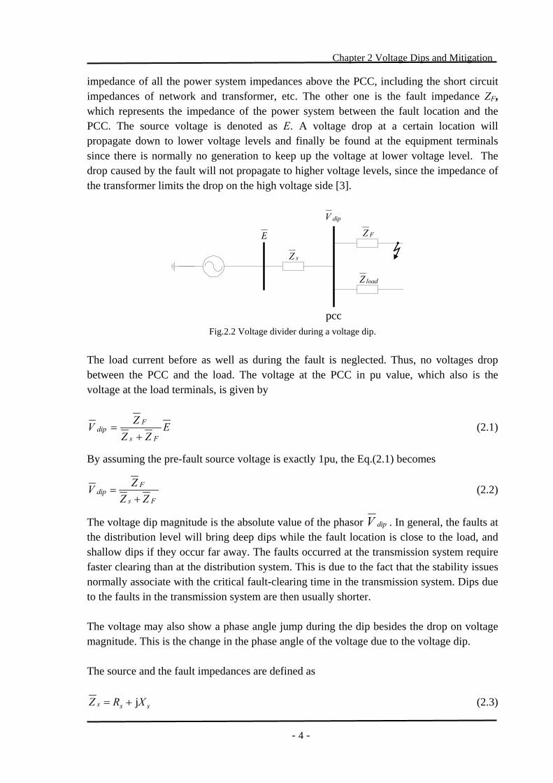
2.1 Characteristic of voltage dips According to IEC-61000-4-30, a voltage dip event is characterized by its magnitude, which is the lowest rms voltage during the event, and its duration, which is the time that the rms voltage stays below the threshold [1]. Thus, the dip magnitude is the retained voltage during the dip. The voltage dip duration depends on the fault clearing time. As the rms value of the voltage cannot change sharply, it is necessary to set a threshold, below which the duration starts to be measured. The dip duration stops when the rms value is above the threshold again. A simplified voltage divider model [2], which is used to calculate the voltage dip in a radial system caused by a fault, is shown in Fig.2.2. The bus between the faulted feeder and the considered load is defined as the Point of Common Coupling (PCC). The PCC is the lowest-voltage bus from which both fault and load are supplied. Two impedances are connected to this bus. One is called source impedance Zs, which is the equivalent
- 3 -
Chapter 2 Voltage Dips and Mitigation
impedance of all the power system impedances above the PCC, including the short circuit impedances of network and transformer, etc. The other one is the fault impedance ZF, which represents the impedance of the power system between the fault location and the PCC. The source voltage is denoted as E. A voltage drop at a certain location will propagate down to lower voltage levels and finally be found at the equipment terminals since there is normally no generation to keep up the voltage at lower voltage level. The drop caused by the fault will not propagate to higher voltage levels, since the impedance of the transformer limits the drop on the high voltage side [3].
FZ
loadZ
sZ
pcc
dipV
E
Fig.2.2 Voltage divider during a voltage dip.
The load current before as well as during the fault is neglected. Thus, no voltages drop between the PCC and the load. The voltage at the PCC in pu value, which also is the voltage at the load terminals, is given by
EZZ
ZVFs
Fdip
+= (2.1)
By assuming the pre-fault source voltage is exactly 1pu, the Eq.(2.1) becomes
Fs
Fdip
ZZZV+
= (2.2)
The voltage dip magnitude is the absolute value of the phasor dipV . In general, the faults at the distribution level will bring deep dips while the fault location is close to the load, and shallow dips if they occur far away. The faults occurred at the transmission system require faster clearing than at the distribution system. This is due to the fact that the stability issues normally associate with the critical fault-clearing time in the transmission system. Dips due to the faults in the transmission system are then usually shorter. The voltage may also show a phase angle jump during the dip besides the drop on voltage magnitude. This is the change in the phase angle of the voltage due to the voltage dip. The source and the fault impedances are defined as
sss XRZ j+= (2.3)
- 4 -
Chapter 2 Voltage Dips and Mitigation
FFF XRZ j+= (2.4)
From the Eq.(2.2), the argument of the phasor dipV , i.e. the phase-angle jump Ψ is given by
⎟⎟⎠
⎞⎜⎜⎝
⎛++
−⎟⎟⎠
⎞⎜⎜⎝
⎛==
sF
sF
F
Fdip
RRXX
RX
Vψ arctanarctan)arg( (2.5)
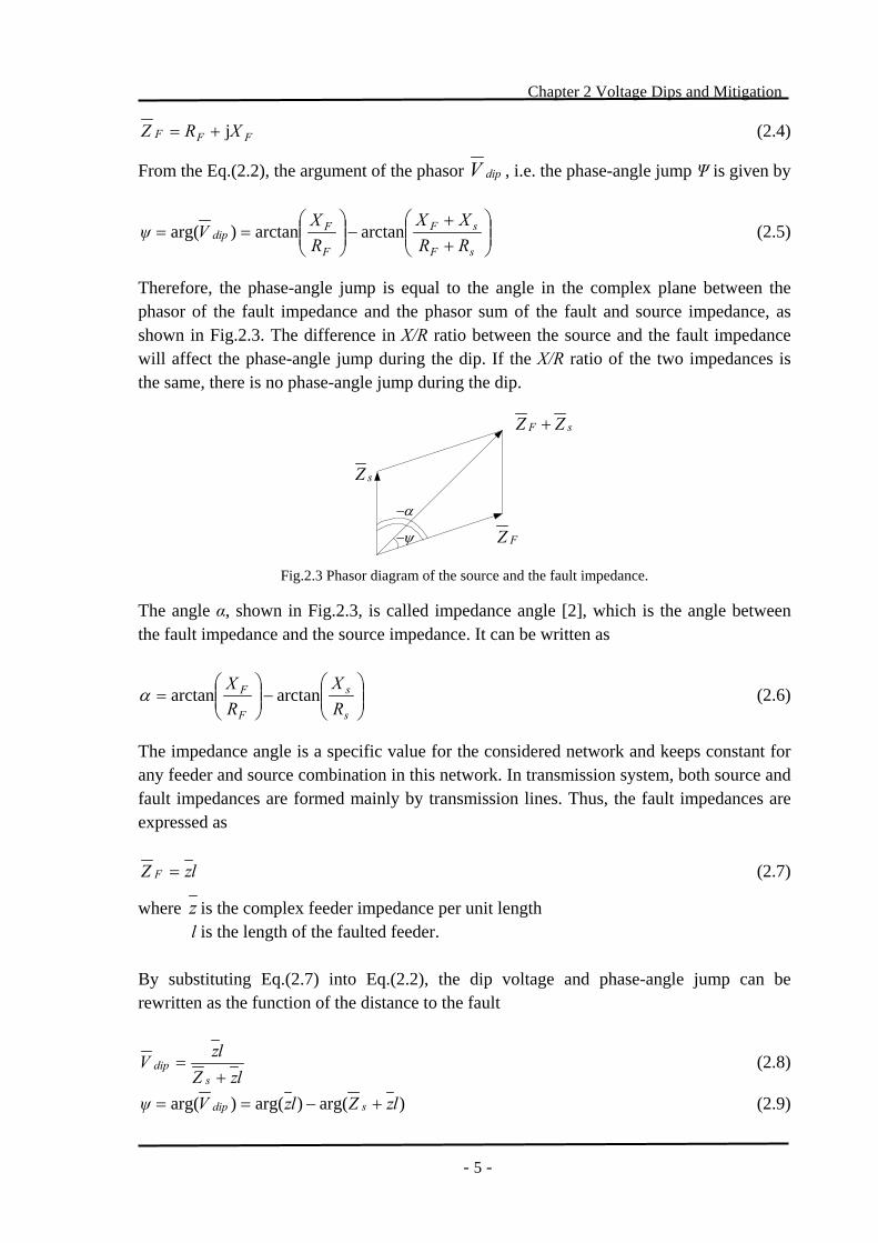
Therefore, the phase-angle jump is equal to the angle in the complex plane between the phasor of the fault impedance and the phasor sum of the fault and source impedance, as shown in Fig.2.3. The difference in X/R ratio between the source and the fault impedance will affect the phase-angle jump during the dip. If the X/R ratio of the two impedances is the same, there is no phase-angle jump during the dip.
ψ−
α−
FZ
sZ
sF ZZ +
Fig.2.3 Phasor diagram of the source and the fault impedance.
The angle α, shown in Fig.2.3, is called impedance angle [2], which is the angle between the fault impedance and the source impedance. It can be written as
⎟⎟⎠
⎞⎜⎜⎝
⎛−⎟⎟
⎠
⎞⎜⎜⎝
⎛=
s
s
F
F
RX
RX
arctanarctanα (2.6)
The impedance angle is a specific value for the considered network and keeps constant for any feeder and source combination in this network. In transmission system, both source and fault impedances are formed mainly by transmission lines. Thus, the fault impedances are expressed as
lzZ F = (2.7)
where z is the complex feeder impedance per unit length l is the length of the faulted feeder.
By substituting Eq.(2.7) into Eq.(2.2), the dip voltage and phase-angle jump can be rewritten as the function of the distance to the fault
lzZlzV
sdip
+= (2.8)
)arg()arg()arg( lzZlzVψ sdip +−== (2.9)
- 5 -
Chapter 2 Voltage Dips and Mitigation
From the phasor diagram Fig.2.3, the phase-angle jump also can be rewritten as
αλλ
αλ
cos21
cos)cos(2 ++
+=ψ (2.10)
where λ, a measure of the ‘electrical’ distance to the fault [2], is defined as
sZlz
=λ (2.11)
Thus, the dip magnitude as a function of the distance to the fault is given by
2)1()cos1(21
11
λ+α−λ
−λ+
λ=dipV (2.12)
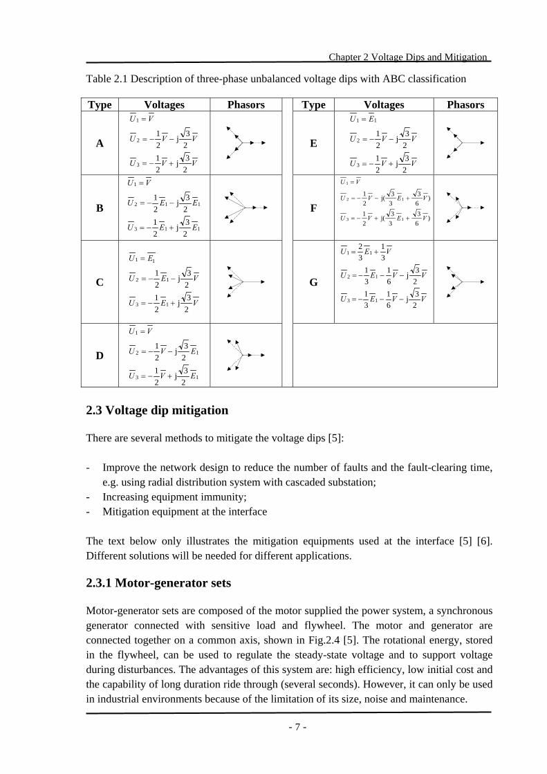
Three-phase unbalanced voltage dips also occur in many cases. To be able to get a better description for a three-phase unbalanced voltage dip, the voltage of sequence component and remaining positive sequence voltage also are used to characterize the voltage dip [2]. 2.2 Voltage dip classification Voltage dip classification is used to describe the three-phase unbalanced dips. The detailed classification methods are reported in [4]. One voltage-dip classification, called ABC classification, used to describe the propagation of dips through transformers is presented briefly in Table 2.1. The complex voltage in the faulted phase or between the faulted phases is denoted by V . The complex pre-fault voltage of phase a is denoted by 1E . The complex three-phase voltages during the fault are denoted by 1U , 2U and 3U . In the phasors diagram, the dashed line is the pre-fault voltage and the solid line is the voltage during the fault. This classification can also be used for testing of equipment against voltage dips.
- 6 -
Chapter 2 Voltage Dips and Mitigation
Table 2.1 Description of three-phase unbalanced voltage dips with ABC classification Type Voltages Phasors Type Voltages Phasors
A
VVU
VVU
VU
23j
21
23j
21
3
2
1
+−=
−−=
=
E
VVU
VVU
EU
23j
21
23j
21
3
2
11
+−=
−−=
=
B
113
112
1
23j
21
23j
21
EEU
EEU
VU
+−=
−−=
=
F
)63
33j(
21
)63
33j(
21
13
12
1
VEVU
VEVU
VU
++−=
+−−=
=
C
VEU
VEU
EU
23j
21
23j
21
13
12
11
+−=
−−=
=
G
VVEU
VVEU
VEU
23j
61
31
23j
61
31
31
32
13
12
11
−−−=
−−−=
+=
D
13
12
1
23j
21
23j
21
EVU
EVU
VU
+−=
−−=
=
2.3 Voltage dip mitigation There are several methods to mitigate the voltage dips [5]: - Improve the network design to reduce the number of faults and the fault-clearing time,
e.g. using radial distribution system with cascaded substation; - Increasing equipment immunity; - Mitigation equipment at the interface The text below only illustrates the mitigation equipments used at the interface [5] [6]. Different solutions will be needed for different applications. 2.3.1 Motor-generator sets Motor-generator sets are composed of the motor supplied the power system, a synchronous generator connected with sensitive load and flywheel. The motor and generator are connected together on a common axis, shown in Fig.2.4 [5]. The rotational energy, stored in the flywheel, can be used to regulate the steady-state voltage and to support voltage during disturbances. The advantages of this system are: high efficiency, low initial cost and the capability of long duration ride through (several seconds). However, it can only be used in industrial environments because of the limitation of its size, noise and maintenance.
- 7 -

Chapter 2 Voltage Dips and Mitigation
Motor GeneratorPowerSystem Load
Fig.2.4 Motor-generator sets.
2.3.2 Transformer-based solutions A constant voltage, or ferro-resonant, transformer can be used to supply a constant voltage to the load during disturbances. This solution is based on a transformer, with a 1:1 turns ratio, working at an operating point, which is always above the knee of its saturation curve. Thus, the output voltage of the transformer maintains constant value no matter how the input voltage varies. To be able to ensure that the transformer works within the expected range of its saturation curve, i.e. the range above the knee of its saturation curve, a capacitor is connected to the secondary winding in the practical design, as shown in Fig.2.5 [5]. This solution only is suitable for low-power, constant loads, since the tuned circuit on the output can cause problems when variable loads are connected [7].
PowerSystem
Load
Fig.2.5 Ferro-resonant transformer.
Electronic tap changers, shown in Fig.2.6, can be installed on a dedicated transformer for the sensitive load. The load voltage can be maintained by change the turns ratio of the transformer while the input voltage varies. The secondary winding, connected with the load, is separated in a number of sections. Each section is connected or disconnected through a fast static switch. Therefore, the secondary voltage can be regulated in steps. In general, thyristor-based switches that can only be turned on once per cycle are used. Thus, this solution introduces a time delay, at least one half cycle, into the dip compensation.
1
234
PowerSystem Load
StaticSwitch
5 Fig. 2.6 Electronic tap changer.
- 8 -
Chapter 2 Voltage Dips and Mitigation
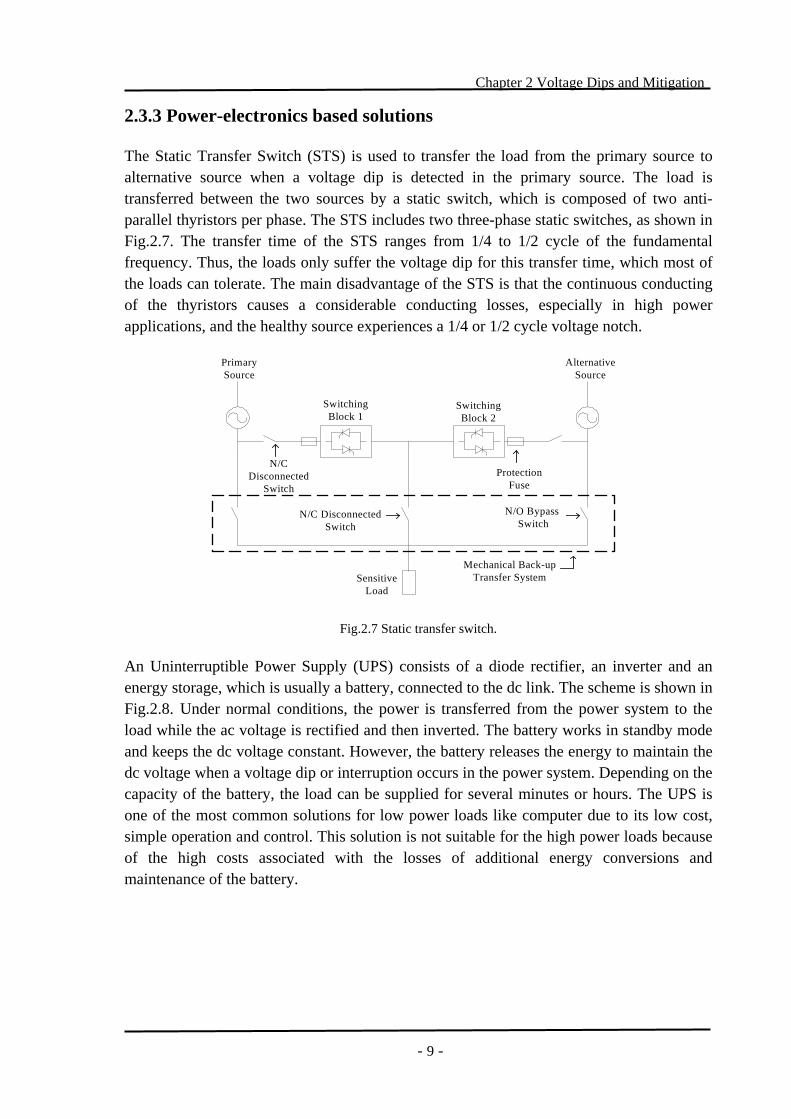
2.3.3 Power-electronics based solutions The Static Transfer Switch (STS) is used to transfer the load from the primary source to alternative source when a voltage dip is detected in the primary source. The load is transferred between the two sources by a static switch, which is composed of two anti- parallel thyristors per phase. The STS includes two three-phase static switches, as shown in Fig.2.7. The transfer time of the STS ranges from 1/4 to 1/2 cycle of the fundamental frequency. Thus, the loads only suffer the voltage dip for this transfer time, which most of the loads can tolerate. The main disadvantage of the STS is that the continuous conducting of the thyristors causes a considerable conducting losses, especially in high power applications, and the healthy source experiences a 1/4 or 1/2 cycle voltage notch.
PrimarySource
SensitiveLoad
SwitchingBlock 1
SwitchingBlock 2
AlternativeSource
N/CDisconnected
Switch
N/C DisconnectedSwitch
N/O Bypass Switch
Mechanical Back-upTransfer System
ProtectionFuse
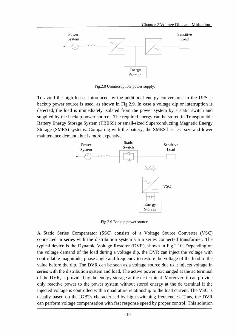
Fig.2.7 Static transfer switch. An Uninterruptible Power Supply (UPS) consists of a diode rectifier, an inverter and an energy storage, which is usually a battery, connected to the dc link. The scheme is shown in Fig.2.8. Under normal conditions, the power is transferred from the power system to the load while the ac voltage is rectified and then inverted. The battery works in standby mode and keeps the dc voltage constant. However, the battery releases the energy to maintain the dc voltage when a voltage dip or interruption occurs in the power system. Depending on the capacity of the battery, the load can be supplied for several minutes or hours. The UPS is one of the most common solutions for low power loads like computer due to its low cost, simple operation and control. This solution is not suitable for the high power loads because of the high costs associated with the losses of additional energy conversions and maintenance of the battery.
- 9 -
Chapter 2 Voltage Dips and Mitigation
EnergyStorage
SensitiveLoad
PowerSystem
Fig.2.8 Uninterruptible power supply.
To avoid the high losses introduced by the additional energy conversions in the UPS, a backup power source is used, as shown in Fig.2.9. In case a voltage dip or interruption is detected, the load is immediately isolated from the power system by a static switch and supplied by the backup power source. The required energy can be stored in Transportable Battery Energy Storage System (TBESS) or small-sized Superconducting Magnetic Energy Storage (SMES) systems. Comparing with the battery, the SMES has less size and lower maintenance demand, but is more expensive.
EnergyStorage
SensitiveLoad
VSC
StaticSwitchPower
System
Fig.2.9 Backup power source.
A Static Series Compensator (SSC) consists of a Voltage Source Converter (VSC) connected in series with the distribution system via a series connected transformer. The typical device is the Dynamic Voltage Restorer (DVR), shown in Fig.2.10. Depending on the voltage demand of the load during a voltage dip, the DVR can inject the voltage with controllable magnitude, phase angle and frequency to restore the voltage of the load to the value before the dip. The DVR can be seen as a voltage source due to it injects voltage in series with the distribution system and load. The active power, exchanged at the ac terminal of the DVR, is provided by the energy storage at the dc terminal. Moreover, it can provide only reactive power to the power system without stored energy at the dc terminal if the injected voltage is controlled with a quadrature relationship to the load current. The VSC is usually based on the IGBTs characterised by high switching frequencies. Thus, the DVR can perform voltage compensation with fast response speed by proper control. This solution
- 10 -
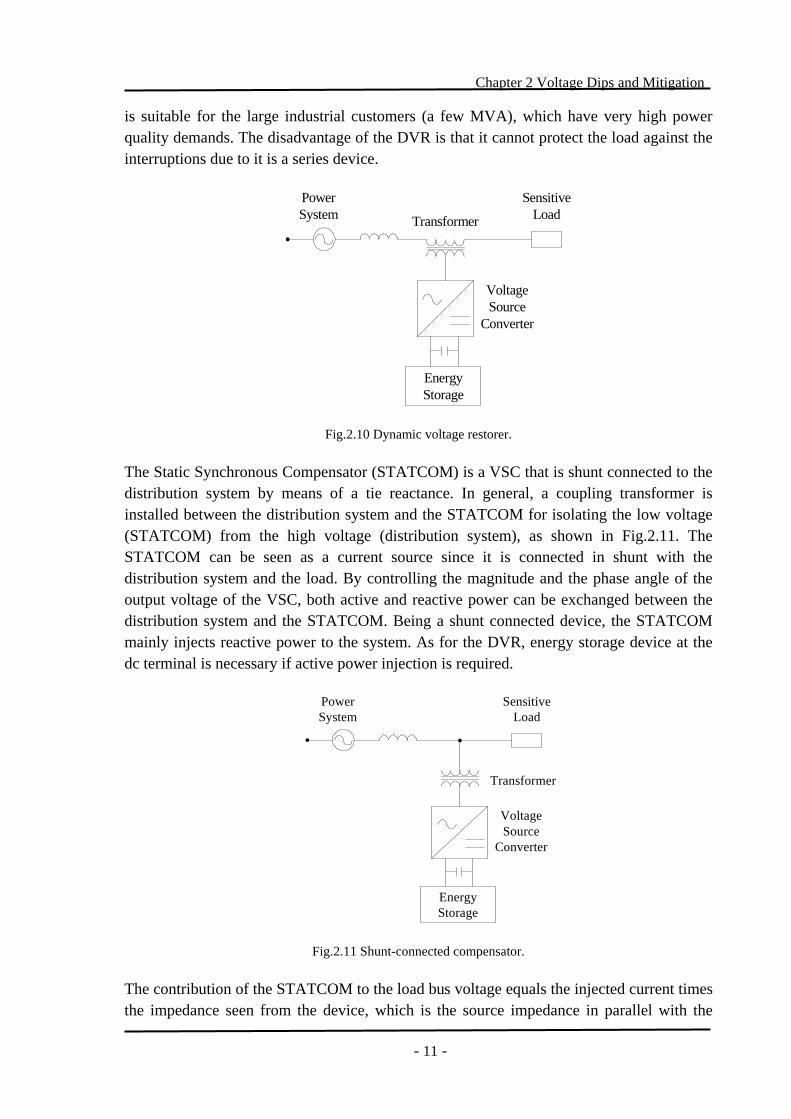
Chapter 2 Voltage Dips and Mitigation
is suitable for the large industrial customers (a few MVA), which have very high power quality demands. The disadvantage of the DVR is that it cannot protect the load against the interruptions due to it is a series device.
EnergyStorage
PowerSystem
SensitiveLoad
VoltageSource
Converter
Transformer
Fig.2.10 Dynamic voltage restorer.
The Static Synchronous Compensator (STATCOM) is a VSC that is shunt connected to the distribution system by means of a tie reactance. In general, a coupling transformer is installed between the distribution system and the STATCOM for isolating the low voltage (STATCOM) from the high voltage (distribution system), as shown in Fig.2.11. The STATCOM can be seen as a current source since it is connected in shunt with the distribution system and the load. By controlling the magnitude and the phase angle of the output voltage of the VSC, both active and reactive power can be exchanged between the distribution system and the STATCOM. Being a shunt connected device, the STATCOM mainly injects reactive power to the system. As for the DVR, energy storage device at the dc terminal is necessary if active power injection is required.
EnergyStorage
PowerSystem
SensitiveLoad
VoltageSource
Converter
Transformer
Fig.2.11 Shunt-connected compensator.
The contribution of the STATCOM to the load bus voltage equals the injected current times the impedance seen from the device, which is the source impedance in parallel with the
- 11 -
Chapter 2 Voltage Dips and Mitigation
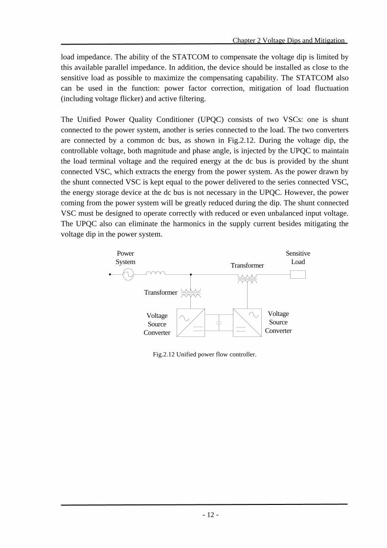
load impedance. The ability of the STATCOM to compensate the voltage dip is limited by this available parallel impedance. In addition, the device should be installed as close to the sensitive load as possible to maximize the compensating capability. The STATCOM also can be used in the function: power factor correction, mitigation of load fluctuation (including voltage flicker) and active filtering. The Unified Power Quality Conditioner (UPQC) consists of two VSCs: one is shunt connected to the power system, another is series connected to the load. The two converters are connected by a common dc bus, as shown in Fig.2.12. During the voltage dip, the controllable voltage, both magnitude and phase angle, is injected by the UPQC to maintain the load terminal voltage and the required energy at the dc bus is provided by the shunt connected VSC, which extracts the energy from the power system. As the power drawn by the shunt connected VSC is kept equal to the power delivered to the series connected VSC, the energy storage device at the dc bus is not necessary in the UPQC. However, the power coming from the power system will be greatly reduced during the dip. The shunt connected VSC must be designed to operate correctly with reduced or even unbalanced input voltage. The UPQC also can eliminate the harmonics in the supply current besides mitigating the voltage dip in the power system.
PowerSystem
SensitiveLoad
VoltageSource
Converter
Transformer
VoltageSource
Converter
Transformer
Fig.2.12 Unified power flow controller.
- 12 -
Chapter 3 Shunt Compenasator for Mitigating Voltage Dips
- 13 -
Chapter 3
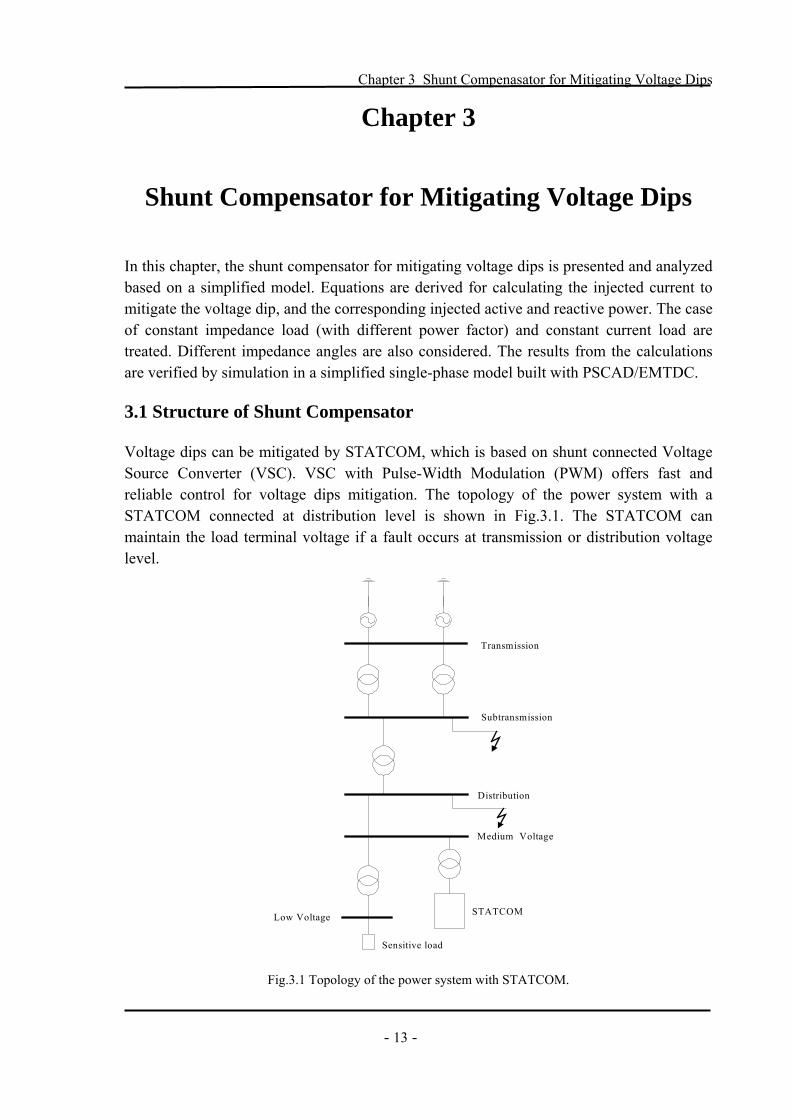
Shunt Compensator for Mitigating Voltage Dips In this chapter, the shunt compensator for mitigating voltage dips is presented and analyzed based on a simplified model. Equations are derived for calculating the injected current to mitigate the voltage dip, and the corresponding injected active and reactive power. The case of constant impedance load (with different power factor) and constant current load are treated. Different impedance angles are also considered. The results from the calculations are verified by simulation in a simplified single-phase model built with PSCAD/EMTDC. 3.1 Structure of Shunt Compensator Voltage dips can be mitigated by STATCOM, which is based on shunt connected Voltage Source Converter (VSC). VSC with Pulse-Width Modulation (PWM) offers fast and reliable control for voltage dips mitigation. The topology of the power system with a STATCOM connected at distribution level is shown in Fig.3.1. The STATCOM can maintain the load terminal voltage if a fault occurs at transmission or distribution voltage level.
STATCOM
Sensitive load
Transmission
Subtransmission
Distribution
Low Voltage
Medium Voltage
Fig.3.1 Topology of the power system with STATCOM.
Chapter 3 Shunt Compenasator for Mitigating Voltage Dips
- 14 -
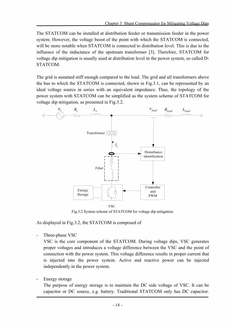
The STATCOM can be installed at distribution feeder or transmission feeder in the power system. However, the voltage boost of the point with which the STATCOM is connected, will be more notable when STATCOM is connected to distribution level. This is due to the influence of the inductance of the upstream transformer [3]. Therefore, STATCOM for voltage dip mitigation is usually used at distribution level in the power system, so called D-STATCOM. The grid is assumed stiff enough compared to the load. The grid and all transformers above the bus to which the STATCOM is connected, shown in Fig.3.1, can be represented by an ideal voltage source in series with an equivalent impedance. Thus, the topology of the power system with STATCOM can be simplified as the system scheme of STATCOM for voltage dip mitigation, as presented in Fig.3.2.
Disturbanceidentification
Controllerand
PWMEnergyStorage
VSC
Filter
se sR sL loadv loadR loadL
ci
Transformer
Fig.3.2 System scheme of STATCOM for voltage dip mitigation.
As displayed in Fig.3.2, the STATCOM is composed of
- Three-phase VSC VSC is the core component of the STATCOM. During voltage dips, VSC generates proper voltages and introduces a voltage difference between the VSC and the point of connection with the power system. This voltage difference results in proper current that is injected into the power system. Active and reactive power can be injected independently in the power system.
- Energy storage The purpose of energy storage is to maintain the DC side voltage of VSC. It can be capacitor or DC source, e.g. battery. Traditional STATCOM only has DC capacitor.
Chapter 3 Shunt Compenasator for Mitigating Voltage Dips
- 15 -
Thus, only reactive power can be injected to the power system by STATCOM. Whereas both active and reactive power can be injected to the power system by STATCOM if DC source is used.
- Filter As the Pulse-Width Modulation (PWM) technique is used in VSC, the output voltage of VSC has switching ripple, which bring harmonics into the current injected to the power system. These harmonics will affect the voltage quality of the power system. Therefore, a relatively small reactor is installed between VSC and the point of the system, with which the STATCOM is connected, to filter those harmonics in the current. The filter can be small if high switching frequency is used. Other alternative filters, e.g. LC filter and LCL filter, will be compared in Chapter 6. A shunt transformer also can filter this harmonic content in the current [8].
- Controller The controller executes the calculation of the correct output voltage of VSC, which leads to proper shunt compensation current, and PWM modulation.
VSC and controller will be illustrated in detail in Chapter 4.
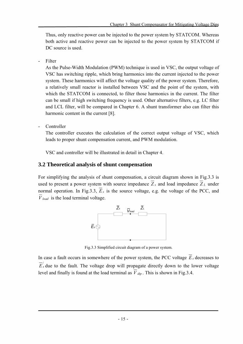
3.2 Theoretical analysis of shunt compensation For simplifying the analysis of shunt compensation, a circuit diagram shown in Fig.3.3 is used to present a power system with source impedance sZ and load impedance LZ under normal operation. In Fig.3.3, sE is the source voltage, e.g. the voltage of the PCC, and
loadV is the load terminal voltage.
Es
Zs ZLVload
Fig.3.3 Simplified circuit diagram of a power system.
In case a fault occurs in somewhere of the power system, the PCC voltage sE decreases to /sE due to the fault. The voltage drop will propagate directly down to the lower voltage
level and finally is found at the load terminal as dipV . This is shown in Fig.3.4.
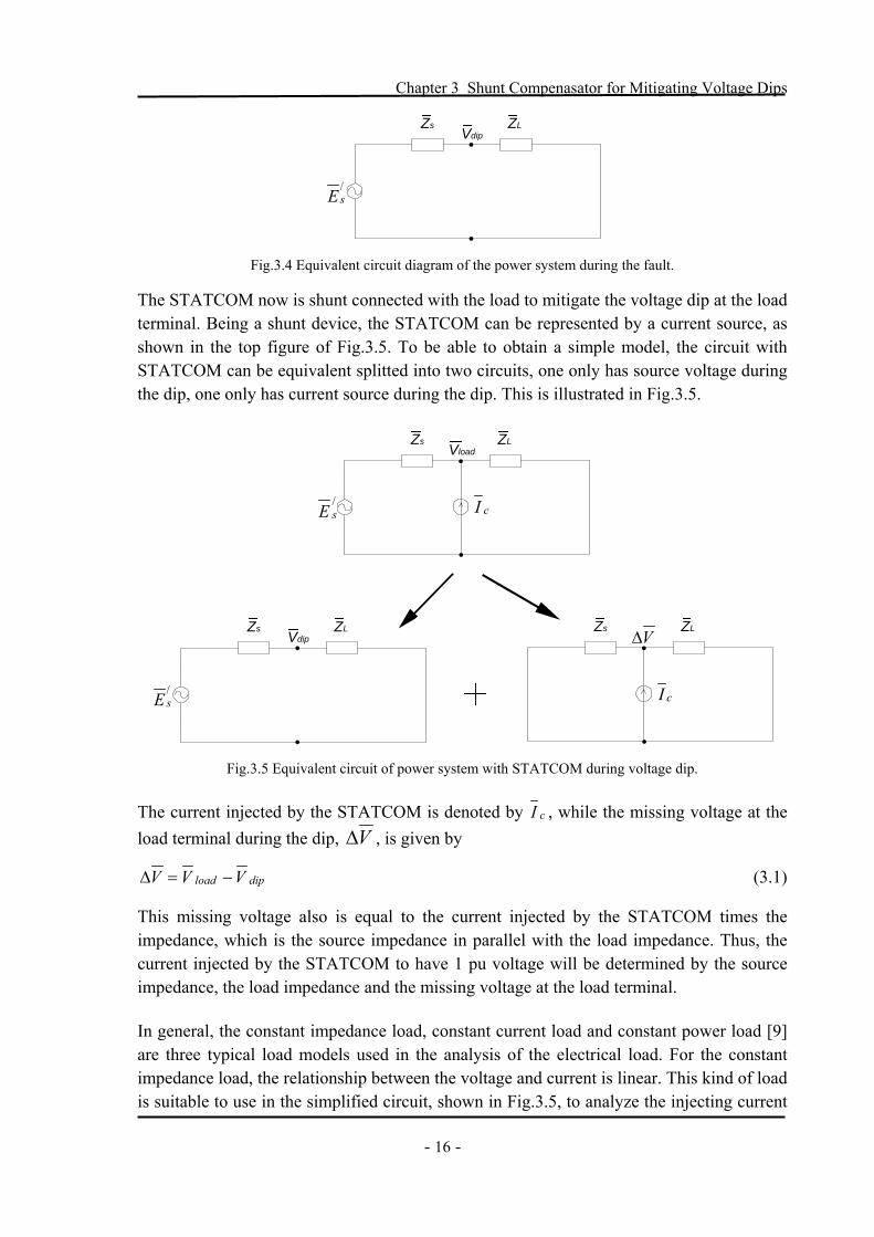
Chapter 3 Shunt Compenasator for Mitigating Voltage Dips
- 16 -
Zs ZLVdip
/sE
Fig.3.4 Equivalent circuit diagram of the power system during the fault.
The STATCOM now is shunt connected with the load to mitigate the voltage dip at the load terminal. Being a shunt device, the STATCOM can be represented by a current source, as shown in the top figure of Fig.3.5. To be able to obtain a simple model, the circuit with STATCOM can be equivalent splitted into two circuits, one only has source voltage during the dip, one only has current source during the dip. This is illustrated in Fig.3.5.
Zs ZLVdip
/sE
Zs ZLVload
/sE
Zs ZL
cI
cI
V∆
Fig.3.5 Equivalent circuit of power system with STATCOM during voltage dip.
The current injected by the STATCOM is denoted by cI , while the missing voltage at the load terminal during the dip, V∆ , is given by
dipload VVV −=∆ (3.1)
This missing voltage also is equal to the current injected by the STATCOM times the impedance, which is the source impedance in parallel with the load impedance. Thus, the current injected by the STATCOM to have 1 pu voltage will be determined by the source impedance, the load impedance and the missing voltage at the load terminal. In general, the constant impedance load, constant current load and constant power load [9] are three typical load models used in the analysis of the electrical load. For the constant impedance load, the relationship between the voltage and current is linear. This kind of load is suitable to use in the simplified circuit, shown in Fig.3.5, to analyze the injecting current
Chapter 3 Shunt Compenasator for Mitigating Voltage Dips
- 17 -
of the STATCOM. The current is constant for a constant current load. Therefore, the load current is independent on the load terminal voltage. Thus, the shunt compensation current only is affected by the source impedance. After the calculation and simulation tests, it is proved that the constant power load is not suitable to use this simplified model, shown in Fig.3.5, to calculate the current injected by the STATCOM during the dip. This is due to the fact that the relationship between the current and the voltage of the constant power load is not linear. The constant impedance load and the constant current load model will be analyzed following. As the load characteristic is different for the constant impedance load and the constant current load, the current injected by the STATCOM to mitigate the dip is different. For the constant impedance load, the injecting current of the STATCOM is
)( diploadLs
Lsc VV
ZZZZI −+
= (3.2)
The complex dip voltage is given by
)sinj(cos ψψVV dipdip −= (3.3)
The load voltage before the fault is considered as reference voltage, i.e. 1 pu. The Eq.(3.2) in pu value becomes
)1( dipLs
Lsc V
ZZZZI −+
= (3.4)
However, the constant current load will keep its current constant during the fault. That also means that all injected current of the STATCOM only flows through the source impedance. Thus, the constant current load branch can be considered as open circuit under this situation. The current injected by the STATCOM during the dip is given by
)(1dipload
sc VV
ZI −= (3.5)
If the load voltage before the fault is considered as exactly 1 pu, Eq.(3.5) can be expressed as
)1(1dip
sc V
ZI −= (3.6)
The source impedance will become very small for faults at the same bus with the STATCOM. This will draw huge current from the STATCOM to mitigate the voltage dip. It is not intelligent method to use the STATCOM in this situation.
Chapter 3 Shunt Compenasator for Mitigating Voltage Dips
- 18 -
In power system analysis, the active power is generally related to the phase angle of the voltage, whereas the reactive power is mostly related to the amplitude of the voltage. In case there is no phase-angle jump in the voltage dip, the voltage can be compensated only by injecting reactive power. However, both active and reactive power are needed to compensate the voltage dip if both the voltage magnitude and phase angle are changed during the dip and both must be restored. The apparent power injected by the STATCOM is calculated by
*cload IVS = (3.7)
*cI is the conjugate of the shunt compensation current. If the load voltage is assumed as
exactly 1 pu, Eq.(3.7) can be rewritten as
*cIS = (3.8)
The real part of the apparent power is the injected active power of the STATCOM. The injected reactive power of the STATCOM is equal to the imaginary part of the apparent power. To study the relationship between the injecting current of the STATCOM and the dip magnitude, the factor λ , a measure of the ‘electrical’ distance to the fault, is derived from Eq.(2.12)
2
222
1sin1cos
dip
dipdipdip
VVVV
−
α−+α=λ (3.9)
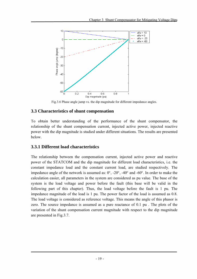
By combined with the Eq.(2.10), the phase-angle jump can be written as a function of the impedance angle and the dip magnitude. Normally, there are four values of the impedance angle [2] used in the power system analysis: 0 is a common value for transmission system faults; +10 is the highest expected value for transmission system faults; -20 corresponds to overhead distribution lines; and –60 to underground distribution cables. The relationship between dip magnitude and phase-angle jump for different impedance angle is shown in Fig.3.6. There is no phase angle jump during the dip if the impedance angle is zero. The phase angle jump during the dip increases (in absolute value) as the dip magnitude decreases.
Chapter 3 Shunt Compenasator for Mitigating Voltage Dips
- 19 -
Fig.3.6 Phase angle jump vs. the dip magnitude for different impedance angles.
3.3 Characteristics of shunt compensation To obtain better understanding of the performance of the shunt compensator, the relationship of the shunt compensation current, injected active power, injected reactive power with the dip magnitude is studied under different situations. The results are presented below. 3.3.1 Different load characteristics The relationship between the compensation current, injected active power and reactive power of the STATCOM and the dip magnitude for different load characteristics, i.e. the constant impedance load and the constant current load, are studied respectively. The impedance angle of the network is assumed as: 0°, -20°, -40° and -60°. In order to make the calculation easier, all parameters in the system are considered as pu value. The base of the system is the load voltage and power before the fault (this base will be valid in the following part of this chapter). Thus, the load voltage before the fault is 1 pu. The impedance magnitude of the load is 1 pu. The power factor of the load is assumed as 0.8. The load voltage is considered as reference voltage. This means the angle of this phasor is zero. The source impedance is assumed as a pure reactance of 0.1 pu . The plots of the variation of the shunt compensation current magnitude with respect to the dip magnitude are presented in Fig.3.7.
Chapter 3 Shunt Compenasator for Mitigating Voltage Dips
- 20 -
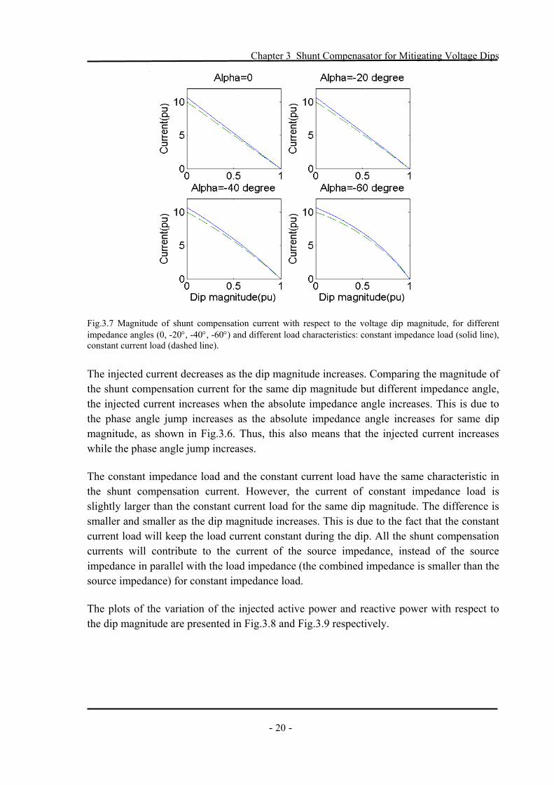
Fig.3.7 Magnitude of shunt compensation current with respect to the voltage dip magnitude, for different impedance angles (0, -20°, -40°, -60°) and different load characteristics: constant impedance load (solid line), constant current load (dashed line). The injected current decreases as the dip magnitude increases. Comparing the magnitude of the shunt compensation current for the same dip magnitude but different impedance angle, the injected current increases when the absolute impedance angle increases. This is due to the phase angle jump increases as the absolute impedance angle increases for same dip magnitude, as shown in Fig.3.6. Thus, this also means that the injected current increases while the phase angle jump increases. The constant impedance load and the constant current load have the same characteristic in the shunt compensation current. However, the current of constant impedance load is slightly larger than the constant current load for the same dip magnitude. The difference is smaller and smaller as the dip magnitude increases. This is due to the fact that the constant current load will keep the load current constant during the dip. All the shunt compensation currents will contribute to the current of the source impedance, instead of the source impedance in parallel with the load impedance (the combined impedance is smaller than the source impedance) for constant impedance load. The plots of the variation of the injected active power and reactive power with respect to the dip magnitude are presented in Fig.3.8 and Fig.3.9 respectively.
Chapter 3 Shunt Compenasator for Mitigating Voltage Dips
- 21 -
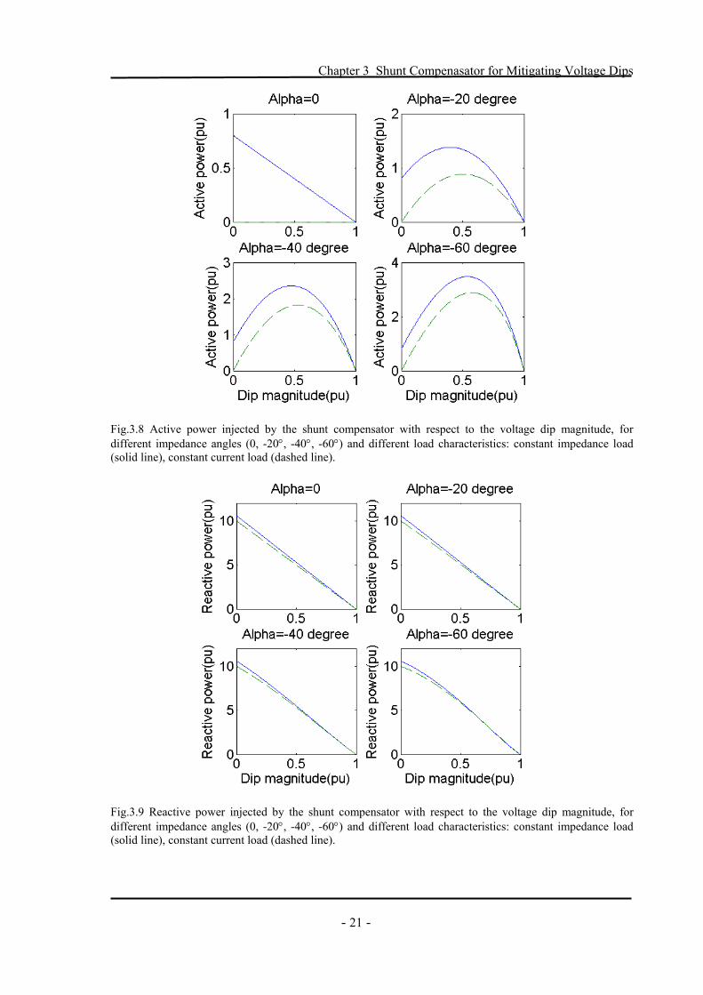
Fig.3.8 Active power injected by the shunt compensator with respect to the voltage dip magnitude, for different impedance angles (0, -20°, -40°, -60°) and different load characteristics: constant impedance load (solid line), constant current load (dashed line).
Fig.3.9 Reactive power injected by the shunt compensator with respect to the voltage dip magnitude, for different impedance angles (0, -20°, -40°, -60°) and different load characteristics: constant impedance load (solid line), constant current load (dashed line).
Chapter 3 Shunt Compenasator for Mitigating Voltage Dips
- 22 -
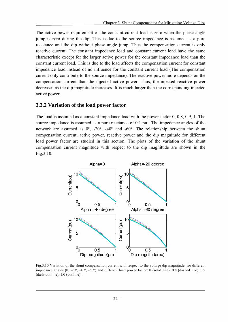
The active power requirement of the constant current load is zero when the phase angle jump is zero during the dip. This is due to the source impedance is assumed as a pure reactance and the dip without phase angle jump. Thus the compensation current is only reactive current. The constant impedance load and constant current load have the same characteristic except for the larger active power for the constant impedance load than the constant current load. This is due to the load affects the compensation current for constant impedance load instead of no influence for the constant current load (The compensation current only contribute to the source impedance). The reactive power more depends on the compensation current than the injected active power. Thus, the injected reactive power decreases as the dip magnitude increases. It is much larger than the corresponding injected active power. 3.3.2 Variation of the load power factor The load is assumed as a constant impedance load with the power factor 0, 0.8, 0.9, 1. The source impedance is assumed as a pure reactance of 0.1 pu . The impedance angles of the network are assumed as 0°, -20°, -40° and -60°. The relationship between the shunt compensation current, active power, reactive power and the dip magnitude for different load power factor are studied in this section. The plots of the variation of the shunt compensation current magnitude with respect to the dip magnitude are shown in the Fig.3.10.
Fig.3.10 Variation of the shunt compensation current with respect to the voltage dip magnitude, for different impedance angles (0, -20°, -40°, -60°) and different load power factor: 0 (solid line), 0.8 (dashed line), 0.9 (dash-dot line), 1.0 (dot line).
Chapter 3 Shunt Compenasator for Mitigating Voltage Dips
- 23 -
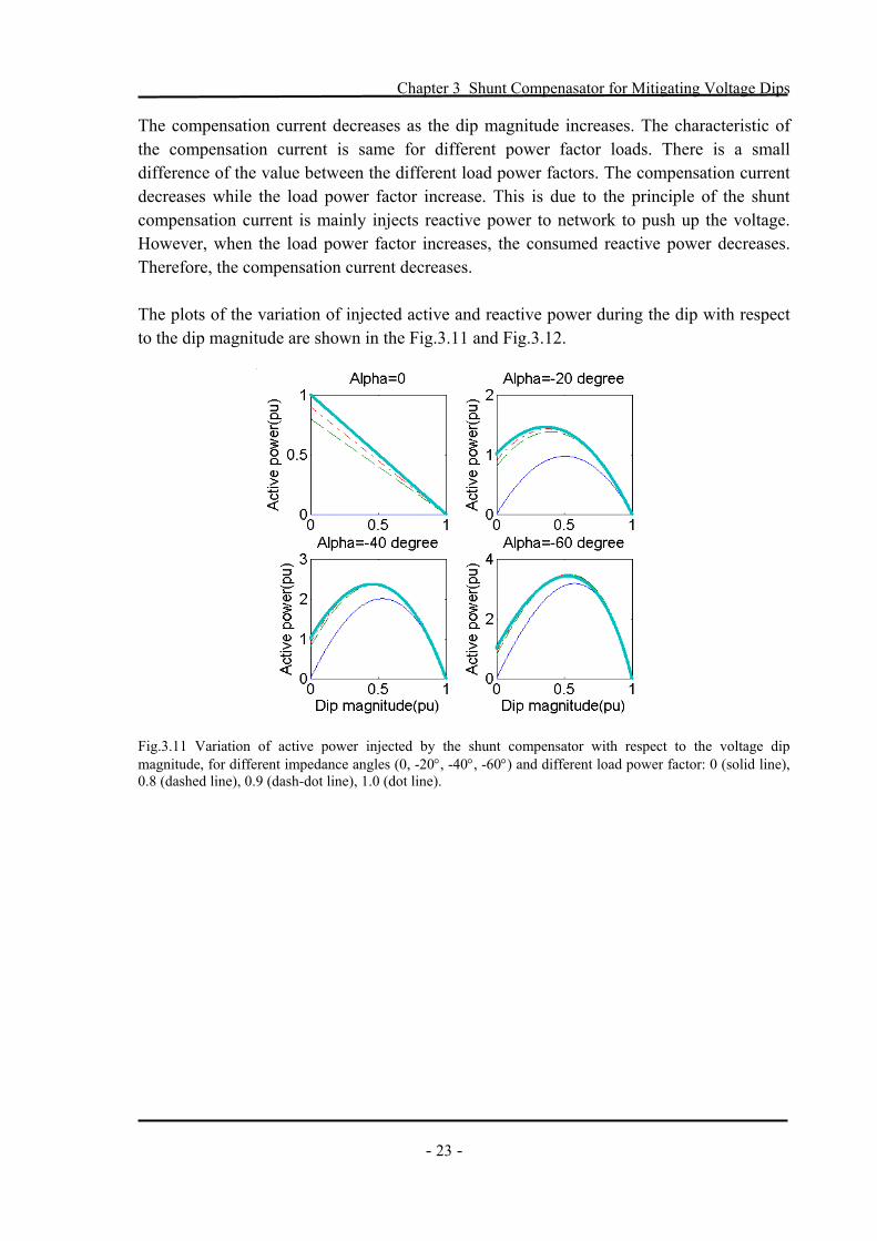
The compensation current decreases as the dip magnitude increases. The characteristic of the compensation current is same for different power factor loads. There is a small difference of the value between the different load power factors. The compensation current decreases while the load power factor increase. This is due to the principle of the shunt compensation current is mainly injects reactive power to network to push up the voltage. However, when the load power factor increases, the consumed reactive power decreases. Therefore, the compensation current decreases. The plots of the variation of injected active and reactive power during the dip with respect to the dip magnitude are shown in the Fig.3.11 and Fig.3.12.
Fig.3.11 Variation of active power injected by the shunt compensator with respect to the voltage dip magnitude, for different impedance angles (0, -20°, -40°, -60°) and different load power factor: 0 (solid line), 0.8 (dashed line), 0.9 (dash-dot line), 1.0 (dot line).
Chapter 3 Shunt Compenasator for Mitigating Voltage Dips
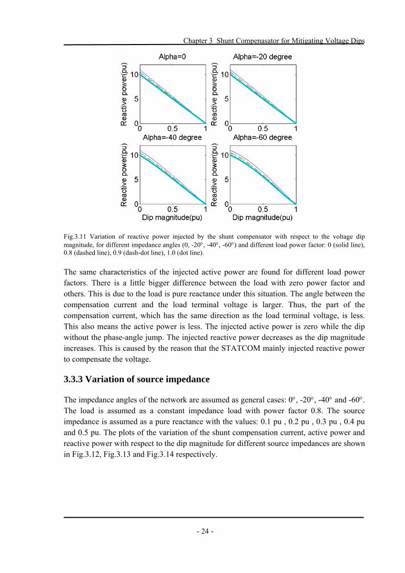
- 24 -
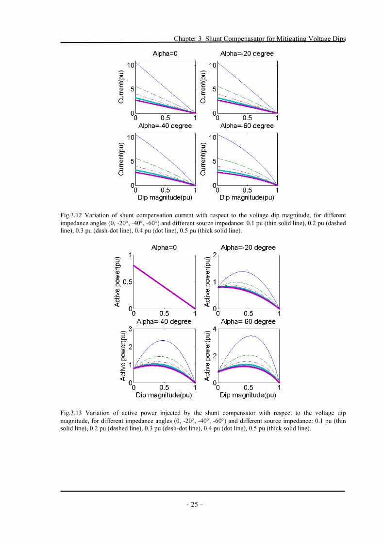
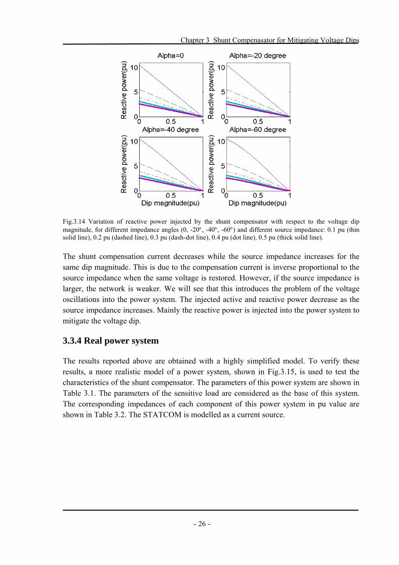
Fig.3.11 Variation of reactive power injected by the shunt compensator with respect to the voltage dip magnitude, for different impedance angles (0, -20°, -40°, -60°) and different load power factor: 0 (solid line), 0.8 (dashed line), 0.9 (dash-dot line), 1.0 (dot line). The same characteristics of the injected active power are found for different load power factors. There is a little bigger difference between the load with zero power factor and others. This is due to the load is pure reactance under this situation. The angle between the compensation current and the load terminal voltage is larger. Thus, the part of the compensation current, which has the same direction as the load terminal voltage, is less. This also means the active power is less. The injected active power is zero while the dip without the phase-angle jump. The injected reactive power decreases as the dip magnitude increases. This is caused by the reason that the STATCOM mainly injected reactive power to compensate the voltage. 3.3.3 Variation of source impedance The impedance angles of the network are assumed as general cases: 0°, -20°, -40° and -60°. The load is assumed as a constant impedance load with power factor 0.8. The source impedance is assumed as a pure reactance with the values: 0.1 pu , 0.2 pu , 0.3 pu , 0.4 pu and 0.5 pu. The plots of the variation of the shunt compensation current, active power and reactive power with respect to the dip magnitude for different source impedances are shown in Fig.3.12, Fig.3.13 and Fig.3.14 respectively.
Chapter 3 Shunt Compenasator for Mitigating Voltage Dips
- 25 -
Fig.3.12 Variation of shunt compensation current with respect to the voltage dip magnitude, for different impedance angles (0, -20°, -40°, -60°) and different source impedance: 0.1 pu (thin solid line), 0.2 pu (dashed line), 0.3 pu (dash-dot line), 0.4 pu (dot line), 0.5 pu (thick solid line).
Fig.3.13 Variation of active power injected by the shunt compensator with respect to the voltage dip magnitude, for different impedance angles (0, -20°, -40°, -60°) and different source impedance: 0.1 pu (thin solid line), 0.2 pu (dashed line), 0.3 pu (dash-dot line), 0.4 pu (dot line), 0.5 pu (thick solid line).
Chapter 3 Shunt Compenasator for Mitigating Voltage Dips
- 26 -
Fig.3.14 Variation of reactive power injected by the shunt compensator with respect to the voltage dip magnitude, for different impedance angles (0, -20°, -40°, -60°) and different source impedance: 0.1 pu (thin solid line), 0.2 pu (dashed line), 0.3 pu (dash-dot line), 0.4 pu (dot line), 0.5 pu (thick solid line). The shunt compensation current decreases while the source impedance increases for the same dip magnitude. This is due to the compensation current is inverse proportional to the source impedance when the same voltage is restored. However, if the source impedance is larger, the network is weaker. We will see that this introduces the problem of the voltage oscillations into the power system. The injected active and reactive power decrease as the source impedance increases. Mainly the reactive power is injected into the power system to mitigate the voltage dip. 3.3.4 Real power system The results reported above are obtained with a highly simplified model. To verify these results, a more realistic model of a power system, shown in Fig.3.15, is used to test the characteristics of the shunt compensator. The parameters of this power system are shown in Table 3.1. The parameters of the sensitive load are considered as the base of this system. The corresponding impedances of each component of this power system in pu value are shown in Table 3.2. The STATCOM is modelled as a current source.
Chapter 3 Shunt Compenasator for Mitigating Voltage Dips
- 27 -
Sub-transmissionStation
STATCOM
130 kV
130/10 kV
10/6 kV
Sensitiveload
load10 kV O/Hline
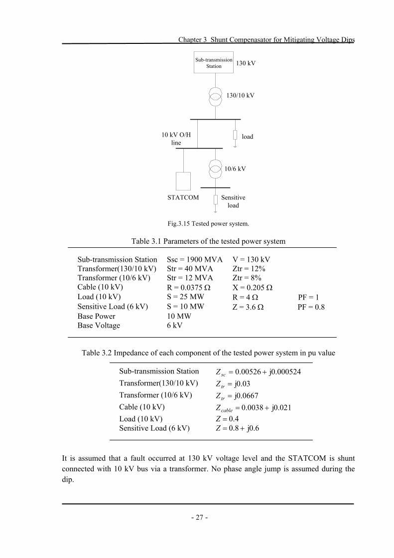
Fig.3.15 Tested power system.
Table 3.1 Parameters of the tested power system
Sub-transmission Station Ssc = 1900 MVA V = 130 kV Transformer(130/10 kV) Str = 40 MVA Ztr = 12% Transformer (10/6 kV) Str = 12 MVA Ztr = 8% Cable (10 kV) R = 0.0375 Ω X = 0.205 Ω Load (10 kV) S = 25 MW R = 4 Ω PF = 1 Sensitive Load (6 kV) S = 10 MW Z = 3.6 Ω PF = 0.8 Base Power 10 MW Base Voltage 6 kV
Table 3.2 Impedance of each component of the tested power system in pu value
Sub-transmission Station 000524.0j00526.0 +=scZ Transformer(130/10 kV) 03.0j=trZ Transformer (10/6 kV) 0667.0j=trZ Cable (10 kV) 021.0j0038.0 +=cableZ Load (10 kV) 4.0=Z Sensitive Load (6 kV) 6.0j8.0 +=Z
It is assumed that a fault occurred at 130 kV voltage level and the STATCOM is shunt connected with 10 kV bus via a transformer. No phase angle jump is assumed during the dip.

Chapter 3 Shunt Compenasator for Mitigating Voltage Dips
- 28 -
The variation of the compensation current magnitude, active and reactive power with respect to the voltage dip magnitude for different load characteristics, constant impedance load and constant current load, are studied. The results are presented in Fig.3.16.
Fig.3.16 Variation of the current, active and reactive power injected by the shunt compensator with respect to the dip magnitude for different load characteristics: constant impedance load (solid line), constant current load (dashed line). The injected current and the reactive power decrease while the dip magnitude increases. There is slightly difference between the constant impedance load and constant current load in the injected current and the reactive power. The injected active power linearly decreases with the dip magnitude increases since the voltage dip is assumed without phase angle jump. These characteristics are same with the results mentioned in section 3.3.1. The STATCOM still is installed at 10 kV voltage level while the fault occurs at the 130 kV voltage level. The phase angle jump is assumed as zero during the dip. The variation of the current magnitude, active and reactive power, injected by the STATCOM, with respect to the voltage dip magnitude for different load power factor, 0.6, 0.8 and 1.0, are reported in Fig.3.17. Only the constant impedance load is considered here.
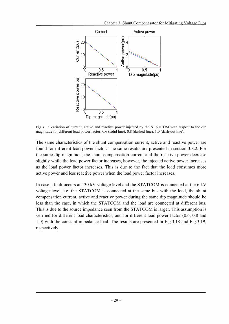
Chapter 3 Shunt Compenasator for Mitigating Voltage Dips
- 29 -
Fig.3.17 Variation of current, active and reactive power injected by the STATCOM with respect to the dip magnitude for different load power factor: 0.6 (solid line), 0.8 (dashed line), 1.0 (dash-dot line). The same characteristics of the shunt compensation current, active and reactive power are found for different load power factor. The same results are presented in section 3.3.2. For the same dip magnitude, the shunt compensation current and the reactive power decrease slightly while the load power factor increases, however, the injected active power increases as the load power factor increases. This is due to the fact that the load consumes more active power and less reactive power when the load power factor increases. In case a fault occurs at 130 kV voltage level and the STATCOM is connected at the 6 kV voltage level, i.e. the STATCOM is connected at the same bus with the load, the shunt compensation current, active and reactive power during the same dip magnitude should be less than the case, in which the STATCOM and the load are connected at different bus. This is due to the source impedance seen from the STATCOM is larger. This assumption is verified for different load characteristics, and for different load power factor (0.6, 0.8 and 1.0) with the constant impedance load. The results are presented in Fig.3.18 and Fig.3.19, respectively.
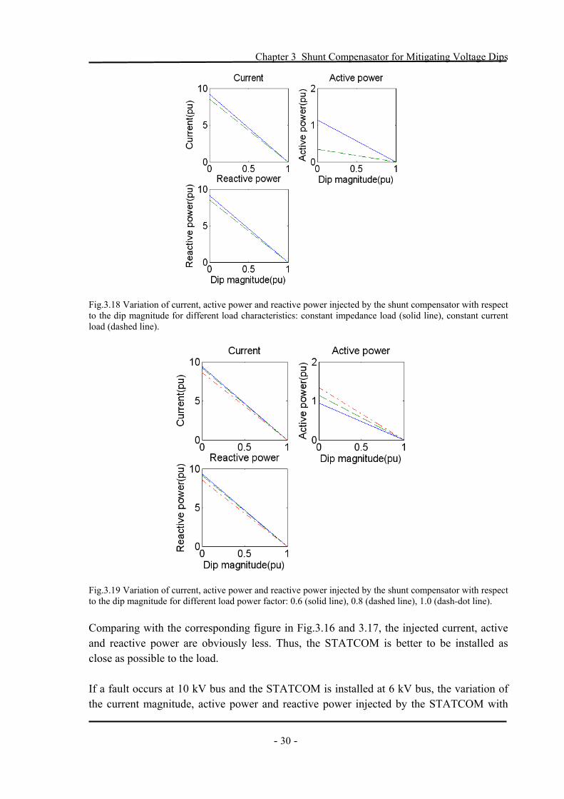
Chapter 3 Shunt Compenasator for Mitigating Voltage Dips
- 30 -
Fig.3.18 Variation of current, active power and reactive power injected by the shunt compensator with respect to the dip magnitude for different load characteristics: constant impedance load (solid line), constant current load (dashed line).
Fig.3.19 Variation of current, active power and reactive power injected by the shunt compensator with respect to the dip magnitude for different load power factor: 0.6 (solid line), 0.8 (dashed line), 1.0 (dash-dot line). Comparing with the corresponding figure in Fig.3.16 and 3.17, the injected current, active and reactive power are obviously less. Thus, the STATCOM is better to be installed as close as possible to the load. If a fault occurs at 10 kV bus and the STATCOM is installed at 6 kV bus, the variation of the current magnitude, active power and reactive power injected by the STATCOM with
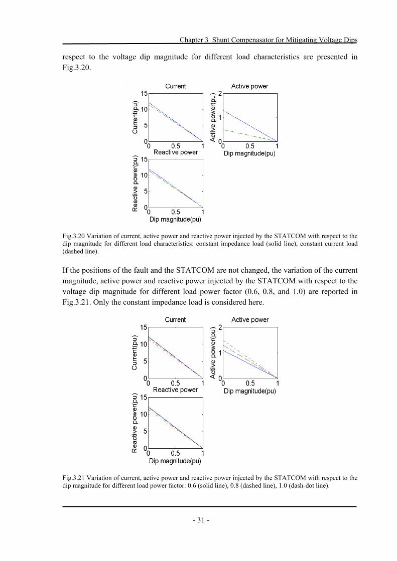
Chapter 3 Shunt Compenasator for Mitigating Voltage Dips
- 31 -
respect to the voltage dip magnitude for different load characteristics are presented in Fig.3.20.
Fig.3.20 Variation of current, active power and reactive power injected by the STATCOM with respect to the dip magnitude for different load characteristics: constant impedance load (solid line), constant current load (dashed line). If the positions of the fault and the STATCOM are not changed, the variation of the current magnitude, active power and reactive power injected by the STATCOM with respect to the voltage dip magnitude for different load power factor (0.6, 0.8, and 1.0) are reported in Fig.3.21. Only the constant impedance load is considered here.
Fig.3.21 Variation of current, active power and reactive power injected by the STATCOM with respect to the dip magnitude for different load power factor: 0.6 (solid line), 0.8 (dashed line), 1.0 (dash-dot line).

Chapter 3 Shunt Compenasator for Mitigating Voltage Dips
- 32 -
Comparing the Fig.3.20 and 3.21 to the Fig.3.18 and 3.19, the larger shunt compensation current, active and reactive power for the same dip magnitude are found in Fig.3.20 and 3.21. This is caused by the source impedance seen from the STATCOM is smaller when the fault is closer to the STATCOM. Thus, the compensation demand of the current, active and reactive power will be increased while the fault is closer to the STATCOM. If the fault and the STATCOM are connected at the same bus, the device will inject huge current to the fault branch. This is verified by assuming that both a fault and STATCOM are connected at 10 kV voltage level. The variation of the current magnitude, active power and reactive power injected by the STATCOM with respect to the voltage dip magnitude are shown in Fig.3.22. The load is considered as a constant impedance load.
Fig.3.22 Variation of current magnitude, active power and reactive power injected by the STATCOM with respect to the dip magnitude. The results show large values of the injected current, active and reactive power. Therefore, the STATCOM usually is not connected to the same bus with the fault. 3.4 Simulation To be able to verify that the shunt compensation current calculated by the Eqs.(3.2) and (3.5) can mitigate the corresponding dip magnitude, the simulation with PSCAD/EMTDC is performed. The results obtained from the calculation with Matlab and from the simulation are compared in this section. 3.4.1 Simulation circuit By assuming a three-phase balanced fault occurs in the system, a single-phase simulation model can be used to simulate the balanced voltage dip. The simulation models for constant impedance load and constant current load are shown in Fig.3.23 and Fig.3.24 respectively.

Chapter 3 Shunt Compenasator for Mitigating Voltage Dips
- 33 -
The source voltage is denoted as E. The simplified source resistance and reactance are denoted as Rs and Ls. The PCC voltage is denoted as Vs. The reactance of the upstream transformer is denoted as Ltr. The voltage and current of the load are denoted as Vload and iload. The resistance and reactance of the load are denoted as Rload and Lload. The shunt compensation current is denoted as ic. The STATCOM is represented by a controllable current source. The resistance and reactance of the fault are denoted as RF and LF. An ideal current source is used to represent the constant current load in the simulation model since the current is constant for this kind of load.
Fault
FL
FR
loadR loadLtrLsR sL
sV loadV loadi
ci
E
. Fig.3.23 Simulation model for constant impedance load.
Fault
FL
FR
trLsR sLsV loadV loadi
ci
E
Fig.3.24 Simulation model for constant current load.
In the simulation model, the parameters of the load are considered as base of the system, i.e. 1 pu . The load parameters used in the simulation are: apparent power of the load is
, rated load voltage is kVA62.1=loadS V230=loadV . The power factor of the load is 0.8. The source impedance is assumed as 0.1 pu and X/R ratio is equal to 10.
3.4.2 Simulation results The simulation is performed by using the calculation shunt compensation current, which is obtained by using Matlab, in the simulation circuit, then observing if the dip voltage can be
Chapter 3 Shunt Compenasator for Mitigating Voltage Dips
- 34 -
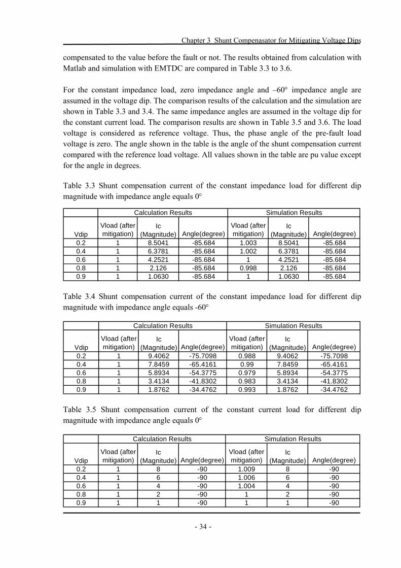
compensated to the value before the fault or not. The results obtained from calculation with Matlab and simulation with EMTDC are compared in Table 3.3 to 3.6. For the constant impedance load, zero impedance angle and –60° impedance angle are assumed in the voltage dip. The comparison results of the calculation and the simulation are shown in Table 3.3 and 3.4. The same impedance angles are assumed in the voltage dip for the constant current load. The comparison results are shown in Table 3.5 and 3.6. The load voltage is considered as reference voltage. Thus, the phase angle of the pre-fault load voltage is zero. The angle shown in the table is the angle of the shunt compensation current compared with the reference load voltage. All values shown in the table are pu value except for the angle in degrees.
Table 3.3 Shunt compensation current of the constant impedance load for different dip magnitude with impedance angle equals 0°
VdipIc
(Magnitude)Ic
(Magnitude)0.2 8.5041 8.50410.4 6.3781 6.37810.6 4.2521 4.25210.8 2.126 2.1260.9 1.0630 1.0630
1
Calculation Results Simulation Results
Vload (aftermitigation) Angle(degree) Angle(degree)
1
Vload (aftermitigation)
1.0031.002
10.998
1
111
-85.684
-85.684-85.684-85.684-85.684-85.684
-85.684-85.684-85.684-85.684
Table 3.4 Shunt compensation current of the constant impedance load for different dip magnitude with impedance angle equals -60°
VdipIc
(Magnitude)Ic
(Magnitude)0.2 9.4062 9.40620.4 7.8459 7.84590.6 5.8934 5.89340.8 3.4134 3.41340.9 1.8762 1.8762 -34.4762
-75.7098-65.4161-54.3775-41.8302-34.4762
-75.7098-65.4161-54.3775-41.8302
1
Vload (aftermitigation)
0.9880.99
0.9790.9830.993
1111
Calculation Results Simulation Results
Vload (aftermitigation) Angle(degree) Angle(degree)
Table 3.5 Shunt compensation current of the constant current load for different dip magnitude with impedance angle equals 0°
VdipIc
(Magnitude)Ic
(Magnitude)0.2 8 80.4 6 60.6 4 40.8 2 20.9 1 1
1
Calculation Results Simulation Results
Vload (aftermitigation) Angle(degree) Angle(degree)
1
Vload (aftermitigation)
1.0091.0061.004
11
111
-90
-90-90-90-90-90
-90-90-90-90

Chapter 3 Shunt Compenasator for Mitigating Voltage Dips
- 35 -
Table 3.6 Shunt compensation current of the constant current load for different dip magnitude with impedance angle equals -60°
VdipIc
(Magnitude)Ic
(Magnitude)0.2 8.8489 8.84890.4 7.3808 7.38080.6 5.5440 5.54400.8 3.2111 3.21110.9 1.765 1.765
1
Calculation Results Simulation Results
Vload (aftermitigation) Angle(degree) Angle(degree)
1
Vload (aftermitigation)
1.0051.0041.0041.0011.004
111
-38.7922
-80.0258-69.7321-58.6936-46.1462-38.7922
-80.0258-69.7321-58.6936-46.1462
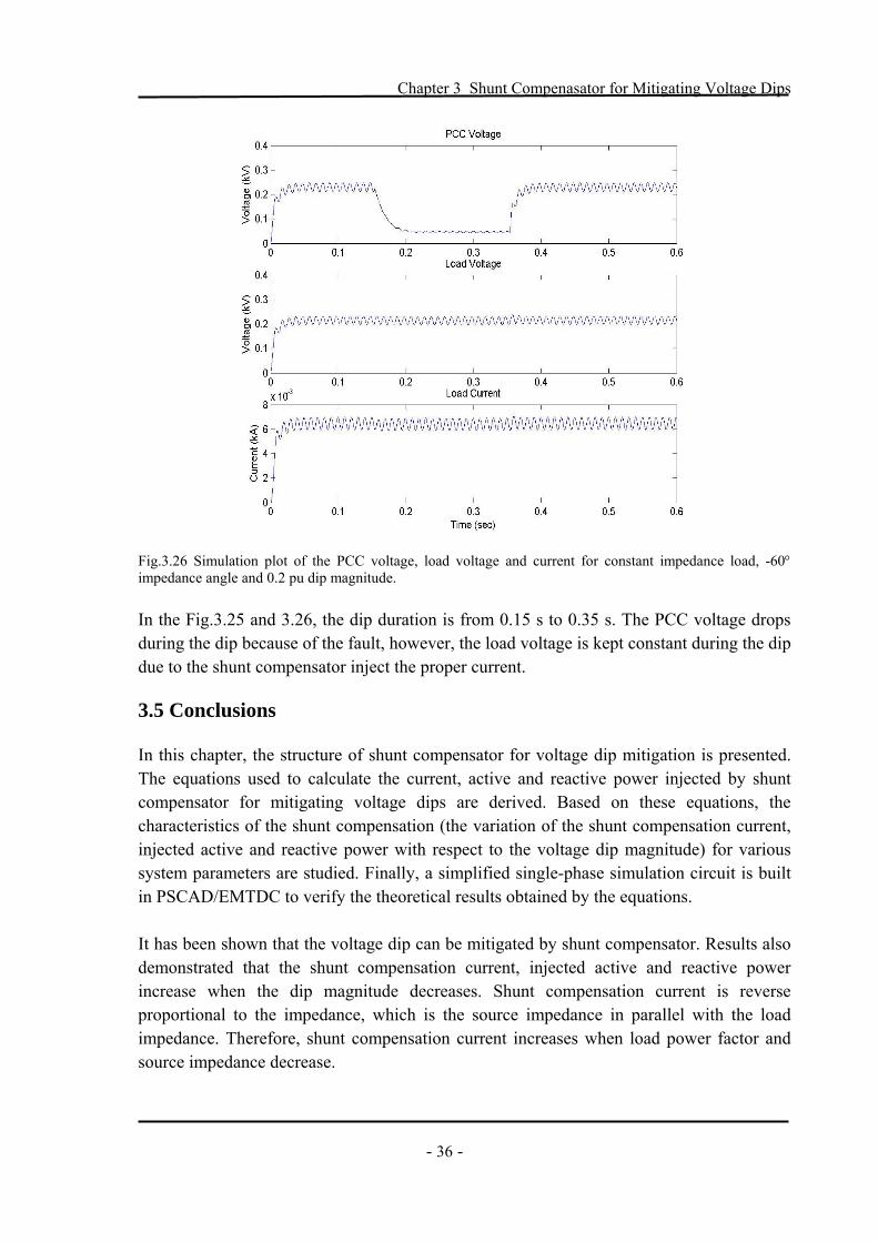
The simulation results matched the calculation results very well in the above tables. The voltage dip can be exactly mitigated by injecting the current, which is calculated by using Eqs.(3.2) and (3.5). For the constant impedance load under 0.2 pu dip magnitude, the simulation plots of the PCC voltage, load voltage and the current are shown in the Fig.3.25 and 3.26. The values shown are rms values. Fig.3.25 shows the dip with zero impedance angle. Fig.3.26 shows the dip with –60° impedance angle.
Fig.3.25 Simulation plot of the PCC voltage, load voltage and current for constant impedance load, zero impedance angle and 0.2 pu dip magnitude.
Chapter 3 Shunt Compenasator for Mitigating Voltage Dips
- 36 -
Fig.3.26 Simulation plot of the PCC voltage, load voltage and current for constant impedance load, -60° impedance angle and 0.2 pu dip magnitude. In the Fig.3.25 and 3.26, the dip duration is from 0.15 s to 0.35 s. The PCC voltage drops during the dip because of the fault, however, the load voltage is kept constant during the dip due to the shunt compensator inject the proper current. 3.5 Conclusions In this chapter, the structure of shunt compensator for voltage dip mitigation is presented. The equations used to calculate the current, active and reactive power injected by shunt compensator for mitigating voltage dips are derived. Based on these equations, the characteristics of the shunt compensation (the variation of the shunt compensation current, injected active and reactive power with respect to the voltage dip magnitude) for various system parameters are studied. Finally, a simplified single-phase simulation circuit is built in PSCAD/EMTDC to verify the theoretical results obtained by the equations. It has been shown that the voltage dip can be mitigated by shunt compensator. Results also demonstrated that the shunt compensation current, injected active and reactive power increase when the dip magnitude decreases. Shunt compensation current is reverse proportional to the impedance, which is the source impedance in parallel with the load impedance. Therefore, shunt compensation current increases when load power factor and source impedance decrease.
Chapter 4 Dual Vector Controller
- 37 -
Chapter 4
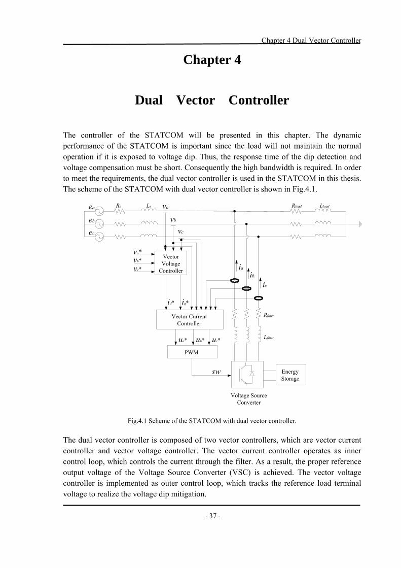
Dual Vector Controller The controller of the STATCOM will be presented in this chapter. The dynamic performance of the STATCOM is important since the load will not maintain the normal operation if it is exposed to voltage dip. Thus, the response time of the dip detection and voltage compensation must be short. Consequently the high bandwidth is required. In order to meet the requirements, the dual vector controller is used in the STATCOM in this thesis. The scheme of the STATCOM with dual vector controller is shown in Fig.4.1.
EnergyStorage
Voltage SourceConverter
ia
ea Rs Ls Rload Lload
VectorVoltage
Controller
Vector CurrentController
PWM
va*vb*vc*
va
vb
vc
eb
ec
ib
ic
id* iq*
ua* ub* uc*
sw
Rfilter
Lfilter
Fig.4.1 Scheme of the STATCOM with dual vector controller.
The dual vector controller is composed of two vector controllers, which are vector current controller and vector voltage controller. The vector current controller operates as inner control loop, which controls the current through the filter. As a result, the proper reference output voltage of the Voltage Source Converter (VSC) is achieved. The vector voltage controller is implemented as outer control loop, which tracks the reference load terminal voltage to realize the voltage dip mitigation.
Chapter 4 Dual Vector Controller
- 38 -
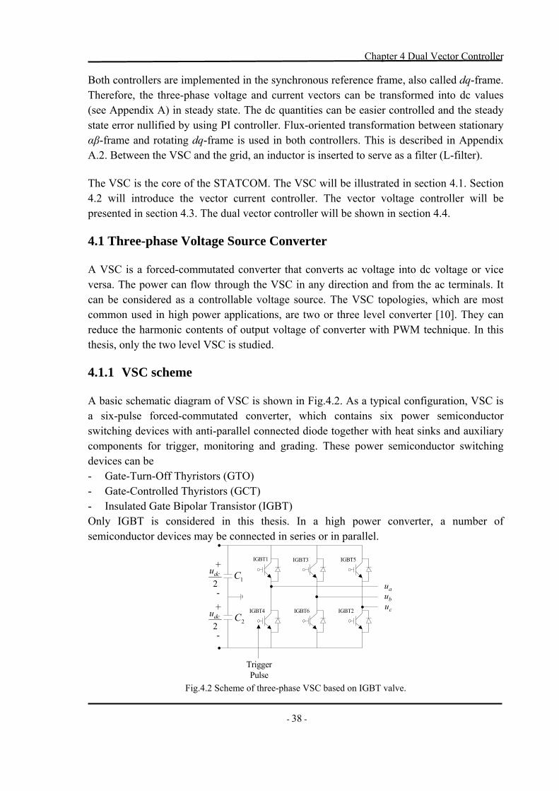
Both controllers are implemented in the synchronous reference frame, also called dq-frame. Therefore, the three-phase voltage and current vectors can be transformed into dc values (see Appendix A) in steady state. The dc quantities can be easier controlled and the steady state error nullified by using PI controller. Flux-oriented transformation between stationary αβ-frame and rotating dq-frame is used in both controllers. This is described in Appendix A.2. Between the VSC and the grid, an inductor is inserted to serve as a filter (L-filter). The VSC is the core of the STATCOM. The VSC will be illustrated in section 4.1. Section 4.2 will introduce the vector current controller. The vector voltage controller will be presented in section 4.3. The dual vector controller will be shown in section 4.4. 4.1 Three-phase Voltage Source Converter A VSC is a forced-commutated converter that converts ac voltage into dc voltage or vice versa. The power can flow through the VSC in any direction and from the ac terminals. It can be considered as a controllable voltage source. The VSC topologies, which are most common used in high power applications, are two or three level converter [10]. They can reduce the harmonic contents of output voltage of converter with PWM technique. In this thesis, only the two level VSC is studied. 4.1.1 VSC scheme A basic schematic diagram of VSC is shown in Fig.4.2. As a typical configuration, VSC is a six-pulse forced-commutated converter, which contains six power semiconductor switching devices with anti-parallel connected diode together with heat sinks and auxiliary components for trigger, monitoring and grading. These power semiconductor switching devices can be - Gate-Turn-Off Thyristors (GTO) - Gate-Controlled Thyristors (GCT) - Insulated Gate Bipolar Transistor (IGBT) Only IGBT is considered in this thesis. In a high power converter, a number of semiconductor devices may be connected in series or in parallel.
+
-2dcu
1C
2C
TriggerPulse
IGBT2
IGBT3
IGBT4
IGBT5
IGBT6
aubucu
+
-2dcu
IGBT1
Fig.4.2 Scheme of three-phase VSC based on IGBT valve.
Chapter 4 Dual Vector Controller
- 39 -
The dc supply of VSC, which is denoted by udc, is stiff if a dc source is used, e.g. a battery. The dc source provides the ability that active power can be exchanged between VSC and power system. When a dc capacitor is used, the dc supply has a slow changing voltage. This is due to the fact that the capacitor needed be charging and discharging during the voltage variation. The dc voltage ripple will be higher when a smaller capacitor is used. However, a high DC peak voltage introduced by large dc capacitor will result in a high requirement of the power rating of the converter [11] [12].
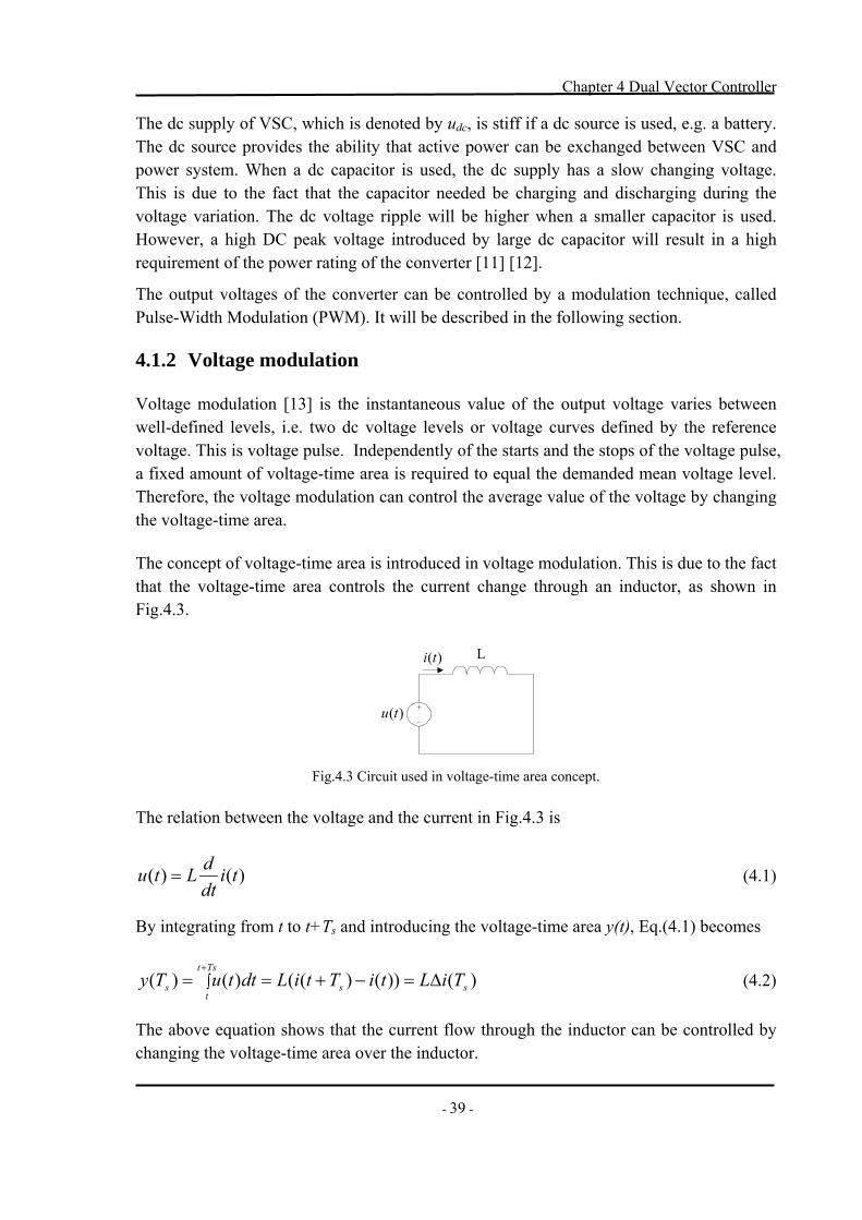
The output voltages of the converter can be controlled by a modulation technique, called Pulse-Width Modulation (PWM). It will be described in the following section. 4.1.2 Voltage modulation Voltage modulation [13] is the instantaneous value of the output voltage varies between well-defined levels, i.e. two dc voltage levels or voltage curves defined by the reference voltage. This is voltage pulse. Independently of the starts and the stops of the voltage pulse, a fixed amount of voltage-time area is required to equal the demanded mean voltage level. Therefore, the voltage modulation can control the average value of the voltage by changing the voltage-time area. The concept of voltage-time area is introduced in voltage modulation. This is due to the fact that the voltage-time area controls the current change through an inductor, as shown in Fig.4.3.
L
)(tu
)(ti
Fig.4.3 Circuit used in voltage-time area concept.
The relation between the voltage and the current in Fig.4.3 is
)()( tidtdLtu = (4.1)
By integrating from t to t+Ts and introducing the voltage-time area y(t), Eq.(4.1) becomes
)())()(()()( ss
Tst
ts TiLtiTtiLdttuTy ∆=−+== ∫
+ (4.2)
The above equation shows that the current flow through the inductor can be controlled by changing the voltage-time area over the inductor.
Chapter 4 Dual Vector Controller
- 40 -
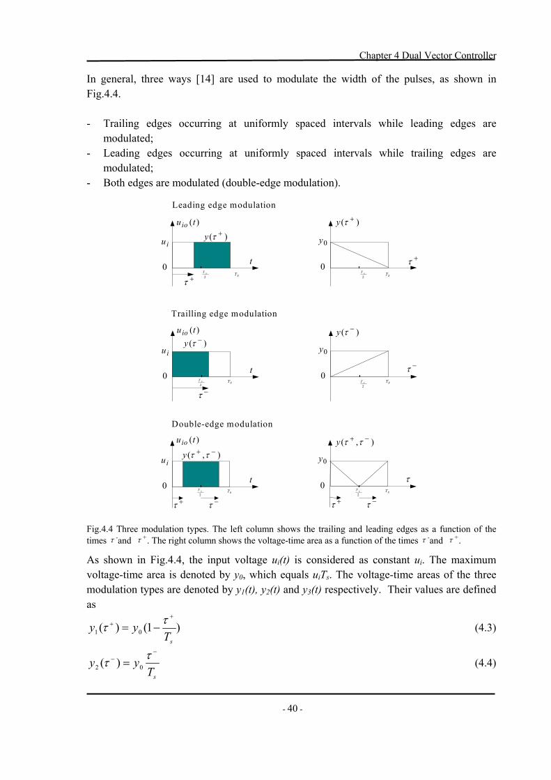
In general, three ways [14] are used to modulate the width of the pulses, as shown in Fig.4.4. - Trailing edges occurring at uniformly spaced intervals while leading edges are
modulated; - Leading edges occurring at uniformly spaced intervals while trailing edges are
modulated; - Both edges are modulated (double-edge modulation).
)(tuio
iu
0+τ
t
)( +τy
0
)( +τy
0y
+τ2
sTsT
2sT
sT
Leading edge modulation
)(tuio
iu
0
−τ2
sT sT
t
)( −τy
0
)( −τy
0y
−τ
2sT sT
Trailling edge modulation
)(tuio
iu
0
−τ2
sT sT
t
+τ
0
−τ2
sT sT
),( −+ ττy
+τ
0y
τ
),( −+ ττy
Double-edge modulation
Fig.4.4 Three modulation types. The left column shows the trailing and leading edges as a function of the timesτ-and τ+. The right column shows the voltage-time area as a function of the timesτ-and τ+.
As shown in Fig.4.4, the input voltage ui(t) is considered as constant ui. The maximum voltage-time area is denoted by y0, which equals uiTs. The voltage-time areas of the three modulation types are denoted by y1(t), y2(t) and y3(t) respectively. Their values are defined as
)1()( 01sT
yy+
+ −=ττ (4.3)
sTyy
−− =
ττ 02 )( (4.4)
Chapter 4 Dual Vector Controller
- 41 -
)21(),( 03
ss TTyy
+−−+ −+=
ττττ (4.5)
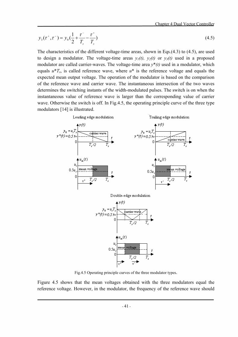
The characteristics of the different voltage-time areas, shown in Eqs.(4.3) to (4.5), are used to design a modulator. The voltage-time areas y1(t), y2(t) or y3(t) used in a proposed modulator are called carrier-waves. The voltage-time area y*(t) used in a modulator, which equals u*Ts, is called reference wave, where u* is the reference voltage and equals the expected mean output voltage. The operation of the modulator is based on the comparison of the reference wave and carrier wave. The instantaneous intersection of the two waves determines the switching instants of the width-modulated pulses. The switch is on when the instantaneous value of reference wave is larger than the corresponding value of carrier wave. Otherwise the switch is off. In Fig.4.5, the operating principle curve of the three type modulators [14] is illustrated.
Fig.4.5 Operating principle curves of the three modulator types.
Figure 4.5 shows that the mean voltages obtained with the three modulators equal the reference voltage. However, in the modulator, the frequency of the reference wave should
Chapter 4 Dual Vector Controller
- 42 -
be much lower than the frequency of the carrier wave. Thus, the reference value can be considered as constant during one sample. 4.1.3 Pulse Width Modulation (PWM) Nowadays Pulse-Width Modulation (PWM) is one most common modulation technique. It is defined as [14]: Pulse Width Modulation essentially involves the sampling of an informational signal (reference wave); This sampled information content is then converted into a series of modulated pulses whose widths reflects the amplitude of the information signal. Three different methods [14] currently being used to achieve PWM switching strategies will be briefly summarized here: nature-sampled PWM, regular-sampled PWM and optimized PWM. Natural-sampled PWM The Natural-sampled PWM is also known as sinusoidal PWM (SPWM). It is based on ‘natural’ sampling techniques and is widely used due to its ease of achievement by using analogue techniques. Natural-sampled PWM is implemented by a direct comparison of a sinusoidal wave (reference wave) and a triangular wave (carrier wave). The instantaneous intersections of the two waves determine the switching instant of the width-modulated pulse. Regular-sampled PWM It is mostly used with digital or microprocessor-based techniques. Regular-sampled PWM is composed of two processes. The first one is Pulse Amplitude Modulation (PAM). It is based on the comparison of the sinusoidal reference wave and the triangular sampling wave. The sinusoidal reference wave is sampled once or twice every carrier cycle. Furthermore, the amplitude of the sampled signal equals the bottom peak value of the triangular sampling wave. As a result of this process, the sampled signal has constant specified amplitude during each sampling interval, i.e. the amplitude is modulated. The second process is Pulse Width Modulation (PWM). The comparison of the sampled signal and the triangular carrier wave is implemented in this process. The intersection points of the two waves determine the switching instant of the width-modulated pulses. Thus, the width of the reference signal is also modulated. One characteristic of Regular-sampled PWM is that the widths of the pulses are proportional to the amplitude of the modulating signal and regularly spaced sampling times. The difference of the sampled number, once or twice, during one carrier cycle result in two different modulation types which are referred to regular sampled ‘symmetric’ and ‘asymmetric’ PWM [14].
Chapter 4 Dual Vector Controller
- 43 -
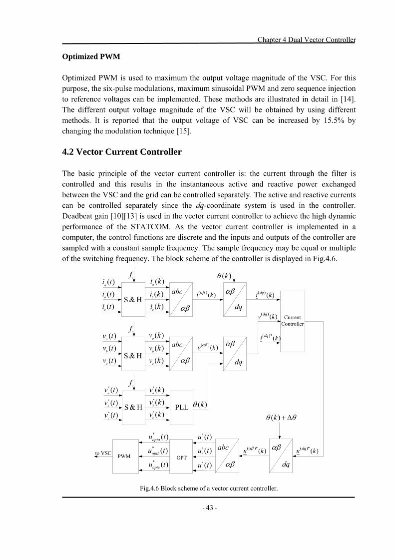
Optimized PWM Optimized PWM is used to maximum the output voltage magnitude of the VSC. For this purpose, the six-pulse modulations, maximum sinusoidal PWM and zero sequence injection to reference voltages can be implemented. These methods are illustrated in detail in [14]. The different output voltage magnitude of the VSC will be obtained by using different methods. It is reported that the output voltage of VSC can be increased by 15.5% by changing the modulation technique [15]. 4.2 Vector Current Controller The basic principle of the vector current controller is: the current through the filter is controlled and this results in the instantaneous active and reactive power exchanged between the VSC and the grid can be controlled separately. The active and reactive currents can be controlled separately since the dq-coordinate system is used in the controller. Deadbeat gain [10][13] is used in the vector current controller to achieve the high dynamic performance of the STATCOM. As the vector current controller is implemented in a computer, the control functions are discrete and the inputs and outputs of the controller are sampled with a constant sample frequency. The sample frequency may be equal or multiple of the switching frequency. The block scheme of the controller is displayed in Fig.4.6.
CurrentController
PWMto VSC
)(tia
)(tib
)(tic
)(tva
)(tvb
)(tvc
)(kia
)(kib
)(kic
)(kva
)(kvb
)(kvc
abc
αβ
abc
αβ
)()( ki αβ
)()( kv αβ
)(* tva
)(* tvb
)(* tvc
H&S
H&S
H&S
)(* kva
)(* kvb
)(* kvc
PLL )(kθ
)(kθ
αβ
αβ
dq
dq)()( ki dq
)()( kv dq
sf
sf
sf
)(*)( ki dq
)(*)( ku dq
dq
αβ
θθ ∆+)(k
)(*)( ku αβ
αβ
abc)(* tua
)(* tub
)(* tuc
OPT
)(* tuopta
)(* tuoptb
)(* tuoptc
Fig.4.6 Block scheme of a vector current controller.

Chapter 4 Dual Vector Controller
- 44 -
In the vector current controller, the grid voltages and filter currents are the inputs of the controller. They are sampled at sample frequency and transformed into the complex reference frame called αβ-frame, then transformed into the rotating dq-frame. The d-axis of this frame is synchronized with the positive-sequence fundamental content of the grid-flux vector. Therefore, the positive-sequence voltages and currents with the fundamental frequency become constant vectors in the dq-frame in steady state. These dc-quantities are used as the inputs of the PI-controller, which is implemented to control and reduce the steady state error. The outputs of the PI-controller are transformed from the dq-frame into the αβ-frame, and then transformed into the abc-coordinate system. In order to extend the output voltage range of the converter [14], a zero-sequence component is added to these three-phase quantities in the OPT block (optimized PWM is used). The outputs of the OPT block are used as the reference voltage for the PWM function of the VSC. 4.2.1 Derivation of the PI-controller System equations The simplified circuit of a grid-connected VSC is displayed in Fig.4.7. The grid and the VSC are modelled as two three-phase voltage sources and L-filter, one in each phase, is in series connected between them. The phase voltages of the VSC are denoted as u1(t), u2(t) and u3(t). The phase voltages of the grid are denoted as v1(t), v2(t) and v3(t). The phase currents through the filter are denoted as i1(t), i2(t) and i3(t). The equivalent inductance and resistance of the L-filter are denoted as L and R, respectively.
1u
2u
3u
VSC
1v
2v
3v
1i
2i
3i
LR
Fig.4.7 Simplified circuit of a grid-connected VSC.
The Kirchhoff voltage law can be applied to the circuit in Fig.4.7. The differential three-phase system equations are
dttdiLRtitvtu )()()()( 1
111 ×+×+= (4.6)
dttdiLRtitvtu )()()()( 2
222 ×+×+= (4.7)
dttdi
LRtitvtu)(
)()()( 3333 ×+×+= (4.8)
The instantaneous grid voltages equal
Chapter 4 Dual Vector Controller
- 45 -
)cos(32)(1 tVtv ω= (4.9)
)32cos(
32)(2 πω −= tVtv (4.10)
)34cos(
32)(3 πω −= tVtv (4.11)
where V is the phase-to-phase rms voltage, and ω is the grid angular frequency. In the αβ-frame, the three-phase system in Eqs.(4.6) to (4.8) becomes
dttdi
LRtitvtu)(
)()()( αααα ×+×+= (4.12)
dttdi
LRtitvtu)(
)()()( ββββ ×+×+= (4.13)
Equations (4.12) and (4.13) can be expressed as continuous state space equations
)()()( tButAxdt
tdx+=
)()()( tDutCxty += (4.14) The system state space equations in αβ-frame can be written as
⎥⎥⎥⎥⎥
⎦
⎤
⎢⎢⎢⎢⎢
⎣
⎡
⎥⎥⎥
⎦
⎤
⎢⎢⎢
⎣
⎡
−
−+⎥
⎦
⎤⎢⎣
⎡
⎥⎥⎥
⎦
⎤
⎢⎢⎢
⎣
⎡
−
−=
⎥⎥⎥
⎦
⎤
⎢⎢⎢
⎣
⎡
)()()()(
1010
0101
)()(
0
0
)(
)(
tvtvtutu
LL
LLtiti
LR
LR
tidtd
tidtd
β
α
β
α
β
α
β
α (4.15)
⎥⎥⎥⎥⎥
⎦
⎤
⎢⎢⎢⎢⎢
⎣
⎡
⎥⎦
⎤⎢⎣
⎡+⎥
⎦
⎤⎢⎣
⎡⎥⎦
⎤⎢⎣
⎡=⎥
⎦
⎤⎢⎣
⎡
)()()()(
00000000
)()(
1001
)()(
tvtvtutu
titi
titi
β
α
β
α
β
α
β
α (4.16)
Equations (4.12) and (4.13) also can be written in vector notation
dttidLRtitvtu )()()()(
)()()()(
αβαβαβαβ ×+×+= (4.17)
where
)(j)()()( tututu βααβ += (4.18)
)(j)()()( tvtvtv βααβ += (4.19)
)(j)()()( tititi βααβ += (4.20)
Chapter 4 Dual Vector Controller
- 46 -
Equation (4.17) can be transferred into the dq-frame by using the αβ to dq transformation giving
)(j)()()()( )()(
)()()( tiLdt
tidLRtitvtu dqdq
dqdqdq ω+×+×+= (4.21) where
)(j)()()( tututu qddq += (4.22)
)(j)()()( tvtvtv qddq += (4.23)
)(j)()()( tititi qddq += (4.24)
Equation (4.21) is splitted into two equations, representing the d and q components respectively, as
)()(
)()()( tLidt
tdiLRtitvtu q
dddd ω−×+×+= (4.25)
)()(
)()()( tLidt
tdiLRtitvtu d
qqqq ω+×+×+= (4.26)
P-controller The vector current controller is implemented in the computer. Thus, the voltages and currents are sampled with the constant sample time Ts. The equivalent inductance and the resistance of the L-filter are denoted as Lr and Rr, which mean these are predicted values. By integrating Eqs.(4.25) and (4.26) from the kTs to (k+1)Ts , the equations become
∫ +−∫ ++∫ +∫ + +∫ += sTkskT dttqirLsTk
skT dtdttddi
rLsTkskT dttdirRsTk
skTsTk
skT dttdvdttdu )1( )()1( )()1( )()1( )1( )()( ω (4.27)
∫ ++∫ ++∫ +∫ + +∫ += sTkskT dttdirLsTk
skT dtdttqdi
rLsTkskT dttqirRsTk
skTsTk
skT dttqvdttqu )1( )()1( )()1( )()1( )1( )()( ω (4.28)
Equations (4.27) and (4.28) are divided by Ts to obtain the average value for the sample period k to k+1
)1,())()1(()1,()1,()1,( +−−+++++=+ kkqirLkdikdisTrL
kkdirRkkdvkkdu ω (4.29)
)1,())()1(()1,()1,()1,( ++−+++++=+ kkdirLkqikqisTrL
kkqirRkkqvkkqu ω (4.30)
In order to achieve high dynamic performance, deadbeat gain is used in the P-controller. The error over one sample period should be zero. For instance, the current at the sample instant k+1 must equal the reference current at the sample instant k. The reference currents are denoted as and . Thus,
*di
*qi
Chapter 4 Dual Vector Controller
- 47 -
)(*)1( kdikdi =+ (4.31)
)(*)1( kqikqi =+ (4.32)
Linear current variation during one sample period is assumed in P-controller, yielding
)(*21
)(21
)1,( kdikdikkdi +=+ (4.33)
)(*21
)(21
)1,( kqikqikkqi +=+ (4.34)
The grid voltages are assumed as constant values within one sample period.
)()1,( kdvkkdv =+ (4.35)
)()1,( kqvkkqv =+ (4.36)
The average values of the VSC voltages during one sample period are assumed to equal the reference voltages, which are denoted as and . Then
*du *
qu
)(*)1,( kdukkdu =+ (4.37)
)(*)1,( kqukkqu =+ (4.38)
Therefore, Eqs.(4.29) and (4.30) can be written as
))()(*()(*2
)(2
)()()(* kdikdipkkqirL
kqirL
kdirRkdvkdu −+−−+=ωω
(4.39)
))()(*()(*2
)(2
)()()(* kqikqipkkdirL
kdirL
kqirRkqvkqu −++++=ωω
(4.40)
where kp is the proportional gain of the P-controller, in which the deadbeat gain is used.
2rR
sTrL
pk += (4.41)
PI-controller An integral term can be added to the P-controller to remove the static error, which is caused by non-linearity, noisy measurements and non-ideal components. Therefore, the PI-controller equations can be written as
)())()(*()(*2
)(2
)()()(* kIdukdikdipkkqirL
kqirL
kdirRkdvkdu ∆+−+−−+=ωω
(4.42)
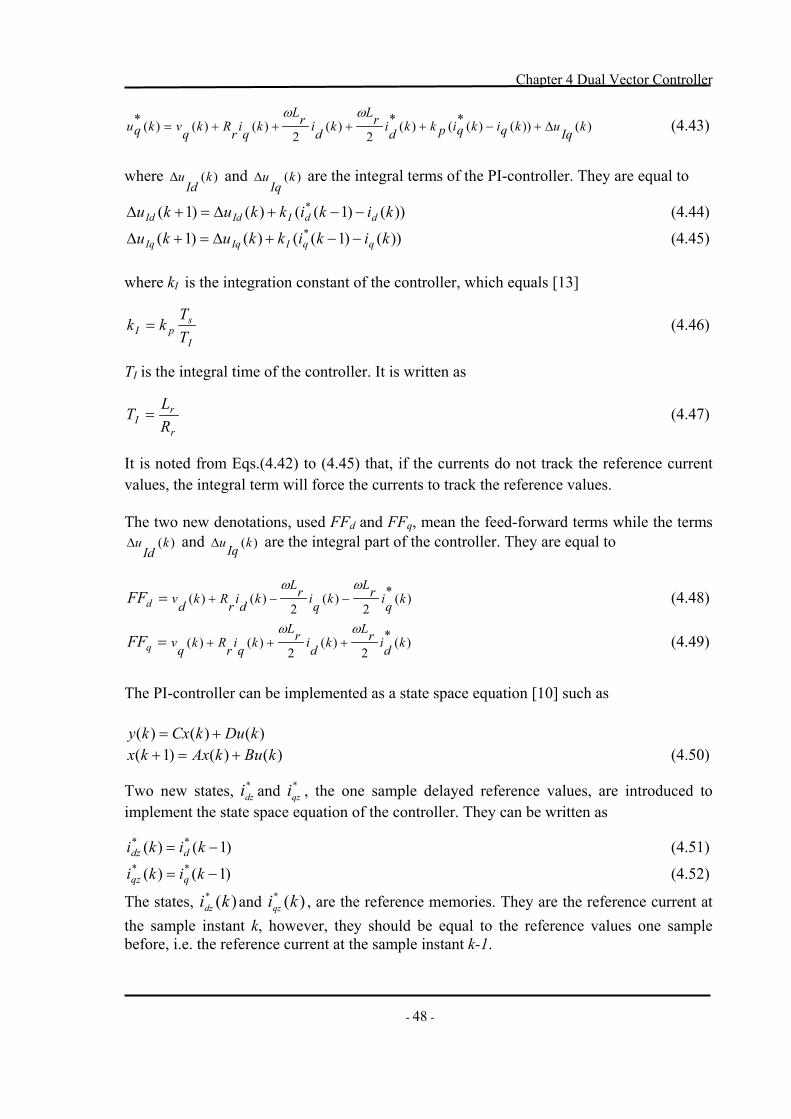
Chapter 4 Dual Vector Controller
- 48 -
)())()(*()(*2
)(2
)()()(* kIqukqikqipkkdirL
kdirL
kqirRkqvkqu ∆+−++++=ωω
(4.43)
where )(kId
u∆ and are the integral terms of the PI-controller. They are equal to )(kIq
u∆
))()1(()()1( * kikikkuku ddIIdId −−+∆=+∆ (4.44)
))()1(()()1( * kikikkuku qqIIqIq −−+∆=+∆ (4.45)
where kI is the integration constant of the controller, which equals [13]
I
spI T
Tkk = (4.46)
TI is the integral time of the controller. It is written as
r
rI R
LT = (4.47)
It is noted from Eqs.(4.42) to (4.45) that, if the currents do not track the reference current values, the integral term will force the currents to track the reference values. The two new denotations, used FFd and FFq, mean the feed-forward terms while the terms
)(kId
u∆ and are the integral part of the controller. They are equal to )(kIqu∆
)(*2
)(2
)()( kqirL
kqirL
kdirRkdvdFFωω
−−+= (4.48)
)(*2
)(2
)()( kdirL
kdirL
kqirRkqvqFFωω
+++= (4.49)
The PI-controller can be implemented as a state space equation [10] such as
)()()( kDukCxky += )()()1( kBukAxkx +=+ (4.50)
Two new states, and , the one sample delayed reference values, are introduced to implement the state space equation of the controller. They can be written as
*dzi *
qzi
)1()( ** −= kiki ddz (4.51)
)1()( ** −= kiki qqz (4.52)
The states, and , are the reference memories. They are the reference current at the sample instant k, however, they should be equal to the reference values one sample before, i.e. the reference current at the sample instant k-1.
)(* kidz )(* kiqz
Chapter 4 Dual Vector Controller
- 49 -
Finally, the PI-controller state space equations can be written as
⎥⎥⎥⎥⎥⎥⎥⎥
⎦
⎤
⎢⎢⎢⎢⎢⎢⎢⎢
⎣
⎡
⎥⎥⎥⎥
⎦
⎤
⎢⎢⎢⎢
⎣
⎡−
−
+
⎥⎥⎥⎥⎥
⎦
⎤
⎢⎢⎢⎢⎢
⎣
⎡∆∆
⎥⎥⎥⎥
⎦
⎤
⎢⎢⎢⎢
⎣
⎡
=
⎥⎥⎥⎥⎥
⎦
⎤
⎢⎢⎢⎢⎢
⎣
⎡
+++∆+∆
)()()()()()(
0000100000010000000000
)()()()(
00000000
010001
)1()1()1()1( *
*
*
*
*
*
kvkvkikikiki
kk
kikikuku
kk
kikikuku
q
d
q
d
q
d
I
I
qz
dz
Iq
Id
I
I
qz
dz
Iq
Id
(4.53)
⎥⎥⎥⎥⎥⎥⎥⎥
⎦
⎤
⎢⎢⎢⎢⎢⎢⎢⎢
⎣
⎡
⎥⎥⎥
⎦
⎤
⎢⎢⎢
⎣
⎡
−
−−−+
⎥⎥⎥⎥⎥
⎦
⎤
⎢⎢⎢⎢⎢
⎣
⎡∆∆
⎥⎦
⎤⎢⎣
⎡=
⎥⎥⎦
⎤
⎢⎢⎣
⎡
)()()()()()(
1022
0122
)()()()(
00100001
)()(
*
*
*
**
*
kvkvkikikiki
kRL
kL
LkR
Lk
kikikuku
kuku
q
d
q
d
q
d
prr
pr
rpr
rp
qz
dz
Iq
Id
q
dωω
ωω (4.54)
4.2.2 Step response The active and reactive current step responses of the vector current controller are simulated by using Matlab/Simulink. Equations (4.15) and (4.16) are used in the simulation model to calculate the filter current in continuous state. The discrete state space equations of the PI-controller, Eqs.(4.53) and (4.54), are implemented in the simulation model to achieve the discrete controller functions. To obtain the discrete signals, which are used in the discrete controller, a block called ‘zero-order hold’ is used in the simulation model to realize the function named ‘sample and hold’. The system parameters used in the simulation are presented in Table 4.1.
Table 4.1 The system parameters used in the simulation model
V = 400 V fs = 2fsw = 10 kHz udc = 850 V fN = 50 Hz L = Lr = 2 mH kp = 20.01 R = Rr = 24.8 mΩ kI = 0.0248
To maximize the current bandwidth, deadbeat gain is used in the P-controller. A step, from 0 to 5 A at 10 ms, is given to the reactive current . The active current is kept at constant value 8 A. The responses of and are shown in Fig.4.8. Vice versa, a step, from
0 to 5 A at 10 ms, is given to the active current . The reactive current is kept at constant value 8 A. The responses of and are shown in Fig.4.9.
*di
*qi
di qi*qi
*di
di qi
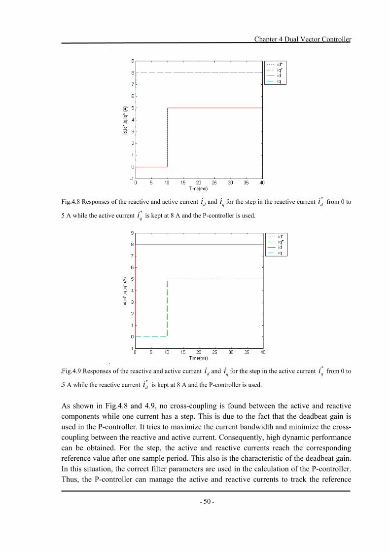
Chapter 4 Dual Vector Controller
- 50 -
Fig.4.8 Responses of the reactive and active current and for the step in the reactive current from 0 to
5 A while the active current is kept at 8 A and the P-controller is used.
di qi*di
*qi
Fig.4.9 Responses of the reactive and active current and for the step in the active current from 0 to di qi
*qi
5 A while the reactive current is kept at 8 A and the P-controller is used. *di
As shown in Fig.4.8 and 4.9, no cross-coupling is found between the active and reactive components while one current has a step. This is due to the fact that the deadbeat gain is used in the P-controller. It tries to maximize the current bandwidth and minimize the cross-coupling between the reactive and active current. Consequently, high dynamic performance can be obtained. For the step, the active and reactive currents reach the corresponding reference value after one sample period. This also is the characteristic of the deadbeat gain. In this situation, the correct filter parameters are used in the calculation of the P-controller. Thus, the P-controller can manage the active and reactive currents to track the reference
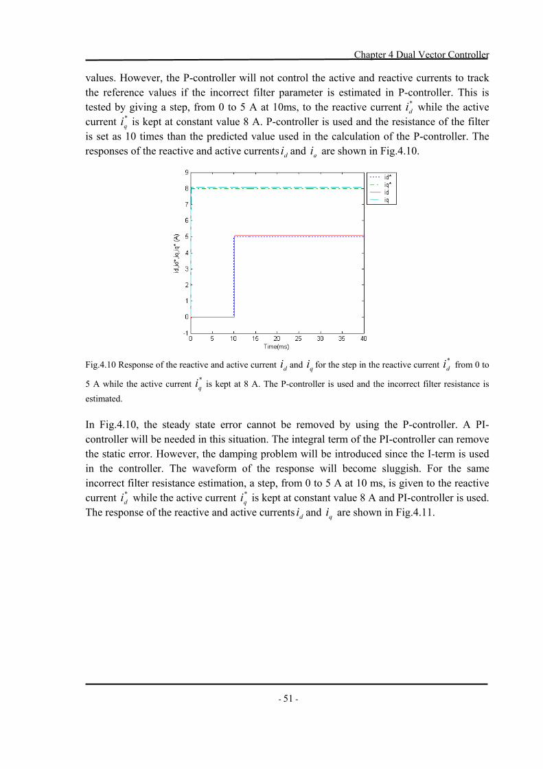
Chapter 4 Dual Vector Controller
- 51 -
values. However, the P-controller will not control the active and reactive currents to track the reference values if the incorrect filter parameter is estimated in P-controller. This is tested by giving a step, from 0 to 5 A at 10ms, to the reactive current while the active current is kept at constant value 8 A. P-controller is used and the resistance of the filter is set as 10 times than the predicted value used in the calculation of the P-controller. The responses of the reactive and active currents and are shown in Fig.4.10.
*di
*qi
di qi
Fig.4.10 Response of the reactive and active current and for the step in the reactive current from 0 to
5 A while the active current is kept at 8 A. The P-controller is used and the incorrect filter resistance is estimated.
di qi*di
*qi
In Fig.4.10, the steady state error cannot be removed by using the P-controller. A PI-controller will be needed in this situation. The integral term of the PI-controller can remove the static error. However, the damping problem will be introduced since the I-term is used in the controller. The waveform of the response will become sluggish. For the same incorrect filter resistance estimation, a step, from 0 to 5 A at 10 ms, is given to the reactive current while the active current is kept at constant value 8 A and PI-controller is used. The response of the reactive and active currents and are shown in Fig.4.11.
*di
*qi
di qi
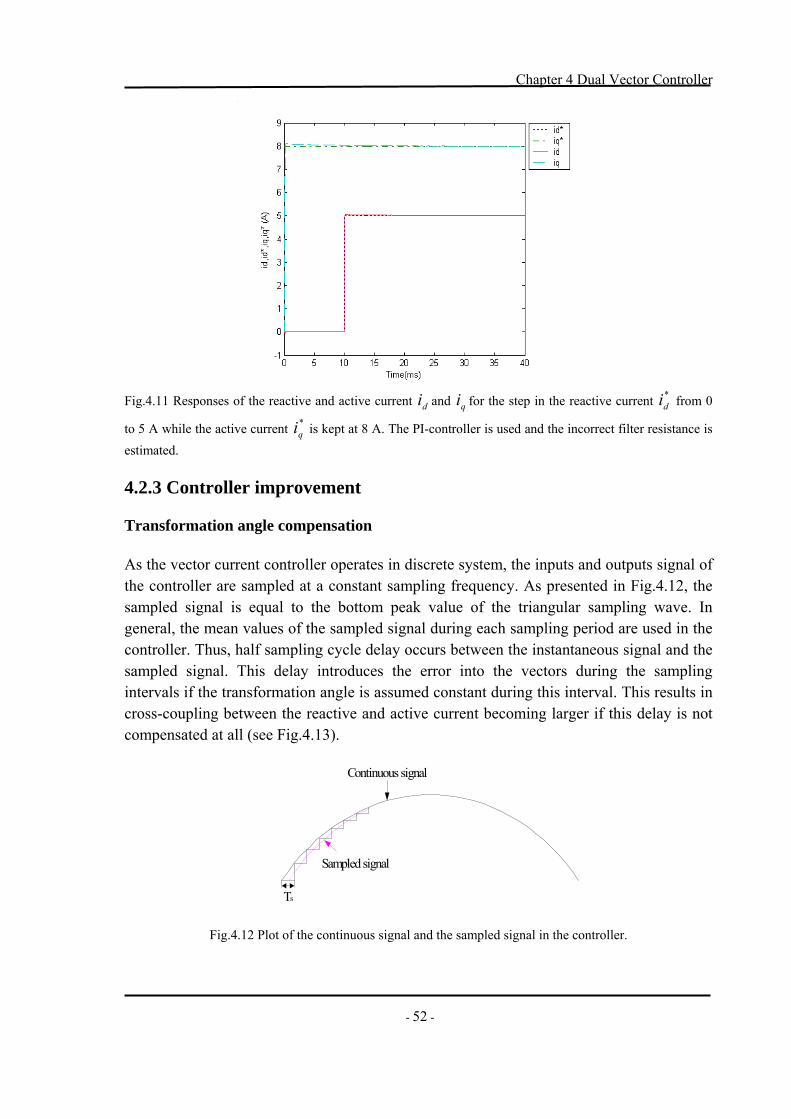
Chapter 4 Dual Vector Controller
- 52 -
Fig.4.11 Responses of the reactive and active current and for the step in the reactive current from 0
to 5 A while the active current is kept at 8 A. The PI-controller is used and the incorrect filter resistance is estimated.
di qi*di
*qi
4.2.3 Controller improvement Transformation angle compensation As the vector current controller operates in discrete system, the inputs and outputs signal of the controller are sampled at a constant sampling frequency. As presented in Fig.4.12, the sampled signal is equal to the bottom peak value of the triangular sampling wave. In general, the mean values of the sampled signal during each sampling period are used in the controller. Thus, half sampling cycle delay occurs between the instantaneous signal and the sampled signal. This delay introduces the error into the vectors during the sampling intervals if the transformation angle is assumed constant during this interval. This results in cross-coupling between the reactive and active current becoming larger if this delay is not compensated at all (see Fig.4.13).
Continuous signal
Sampled signal
Ts
Fig.4.12 Plot of the continuous signal and the sampled signal in the controller.
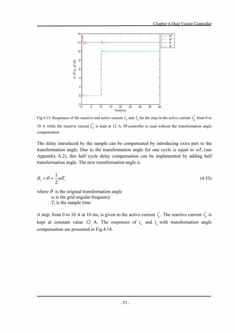
Chapter 4 Dual Vector Controller
- 53 -
Fig.4.13: Responses of the reactive and active current and for the step in the active current from 0 to
10 A while the reactive current is kept at 12 A. PI-controller is used without the transformation angle compensation.
di qi*qi
*di
The delay introduced by the sample can be compensated by introducing extra part to the transformation angle. Due to the transformation angle for one cycle is equal to ωTs (see Appendix A.2), this half cycle delay compensation can be implemented by adding half transformation angle. The new transformation angle is
sTωθθ21
1 += (4.55)
where θ is the original transformation angle ω is the grid angular frequency Ts is the sample time A step, from 0 to 10 A at 10 ms, is given to the active current . The reactive current is kept at constant value 12 A. The responses of and with transformation angle compensation are presented in Fig.4.14.
*qi
*di
di qi
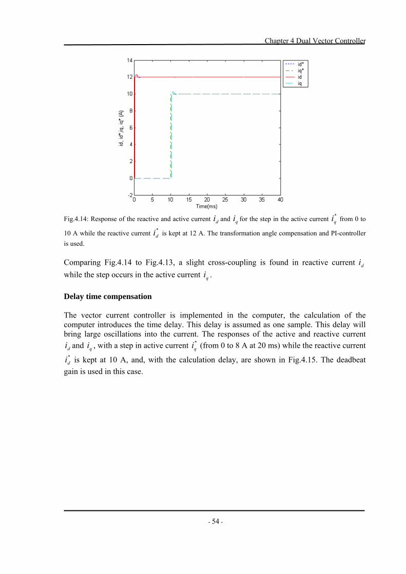
Chapter 4 Dual Vector Controller
- 54 -
Fig.4.14: Response of the reactive and active current and for the step in the active current from 0 to
10 A while the reactive current is kept at 12 A. The transformation angle compensation and PI-controller is used.
di qi*qi
*di
Comparing Fig.4.14 to Fig.4.13, a slight cross-coupling is found in reactive current while the step occurs in the active current .
diqi
Delay time compensation The vector current controller is implemented in the computer, the calculation of the computer introduces the time delay. This delay is assumed as one sample. This delay will bring large oscillations into the current. The responses of the active and reactive current
and , with a step in active current (from 0 to 8 A at 20 ms) while the reactive current
is kept at 10 A, and, with the calculation delay, are shown in Fig.4.15. The deadbeat gain is used in this case.
di qi*qi
*di
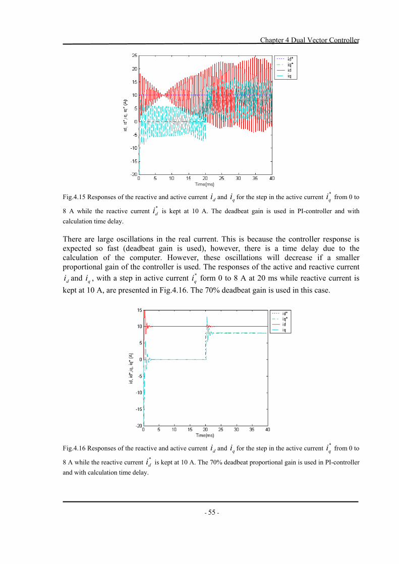
Chapter 4 Dual Vector Controller
- 55 -
Fig.4.15 Responses of the reactive and active current and for the step in the active current from 0 to di qi
*qi
8 A while the reactive current is kept at 10 A. The deadbeat gain is used in PI-controller and with calculation time delay.
*di
There are large oscillations in the real current. This is because the controller response is expected so fast (deadbeat gain is used), however, there is a time delay due to the calculation of the computer. However, these oscillations will decrease if a smaller proportional gain of the controller is used. The responses of the active and reactive current
and , with a step in active current form 0 to 8 A at 20 ms while reactive current is kept at 10 A, are presented in Fig.4.16. The 70% deadbeat gain is used in this case.
di qi*qi
Fig.4.16 Responses of the reactive and active current and for the step in the active current from 0 to di qi
*qi
8 A while the reactive current is kept at 10 A. The 70% deadbeat proportional gain is used in PI-controller and with calculation time delay.
*di
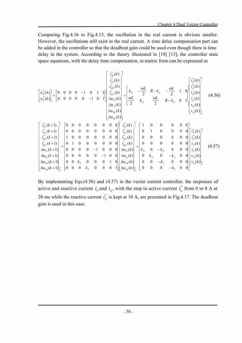
Chapter 4 Dual Vector Controller
- 56 -
Comparing Fig.4.16 to Fig.4.15, the oscillation in the real current is obvious smaller. However, the oscillations still exist in the real current. A time delay compensation part can be added in the controller so that the deadbeat gain could be used even though there is time delay in the system. According to the theory illustrated in [10] [13], the controller state space equations, with the delay time compensation, in matrix form can be expressed as
⎥⎥⎥⎥⎥⎥⎥⎥
⎦
⎤
⎢⎢⎢⎢⎢⎢⎢⎢
⎣
⎡
⎥⎥⎥
⎦
⎤
⎢⎢⎢
⎣
⎡
−
−−−+
⎥⎥⎥⎥⎥⎥⎥⎥⎥⎥⎥
⎦
⎤
⎢⎢⎢⎢⎢⎢⎢⎢⎢⎢⎢
⎣
⎡
∆∆∆∆⎥
⎦
⎤⎢⎣
⎡−
−=
⎥⎥⎦
⎤
⎢⎢⎣
⎡
)()()()()()(
1022
0122
)()()()()()()()(
1010000001010000
)()(
*
*
*
*
*
*
*
*
kvkvkikikiki
kRLkL
LkRLk
kukukukukikikiki
kuku
q
d
q
d
q
d
pp
pp
Iq
Id
q
d
qzz
dzz
qz
dz
q
d
ωω
ωω
(4.56)
⎥⎥⎥⎥⎥⎥⎥⎥
⎦
⎤
⎢⎢⎢⎢⎢⎢⎢⎢
⎣
⎡
⎥⎥⎥⎥⎥⎥⎥⎥⎥⎥⎥
⎦
⎤
⎢⎢⎢⎢⎢⎢⎢⎢⎢⎢⎢
⎣
⎡
−−
−−
+
⎥⎥⎥⎥⎥⎥⎥⎥⎥⎥⎥
⎦
⎤
⎢⎢⎢⎢⎢⎢⎢⎢⎢⎢⎢
⎣
⎡
∆∆∆∆
⎥⎥⎥⎥⎥⎥⎥⎥⎥⎥⎥
⎦
⎤
⎢⎢⎢⎢⎢⎢⎢⎢⎢⎢⎢
⎣
⎡
−−
=
⎥⎥⎥⎥⎥⎥⎥⎥⎥⎥⎥
⎦
⎤
⎢⎢⎢⎢⎢⎢⎢⎢⎢⎢⎢
⎣
⎡
+∆+∆+∆+∆++++
)()()()()()(
000000000000000000000000000000000010000001
)()()()()()()()(
10000000100000001000000001000000000010000000010000000000000000
)1()1()1()1()1()1()1()1(
*
*
*
*
*
*
*
*
*
*
kvkvkikikiki
kk
kkkk
kukukukukikikiki
kk
kukukukukikikiki
q
d
q
d
q
d
I
I
pp
pp
Iq
Id
q
d
qzz
dzz
qz
dz
I
I
Iq
Id
q
d
qzz
dzz
qz
dz
(4.57)
By implementing Eqs.(4.56) and (4.57) in the vector current controller, the responses of active and reactive current and , with the step in active current from 0 to 8 A at di qi
*qi
20 ms while the reactive current is kept at 10 A, are presented in Fig.4.17. The deadbeat gain is used in this case.
*di
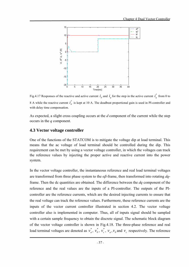
Chapter 4 Dual Vector Controller
- 57 -
Fig.4.17 Responses of the reactive and active current and for the step in the active current from 0 to di qi
*qi
8 A while the reactive current is kept at 10 A. The deadbeat proportional gain is used in PI-controller and with delay time compensation.
*di
As expected, a slight cross coupling occurs at the d component of the current while the step occurs in the q component. 4.3 Vector voltage controller One of the functions of the STATCOM is to mitigate the voltage dip at load terminal. This means that the ac voltage of load terminal should be controlled during the dip. This requirement can be met by using a vector voltage controller, in which the voltages can track the reference values by injecting the proper active and reactive current into the power system. In the vector voltage controller, the instantaneous reference and real load terminal voltages are transformed from three phase system to the αβ-frame, then transformed into rotating dq-frame. Then the dc quantities are obtained. The difference between the dq component of the reference and the real values are the inputs of a PI-controller. The outputs of the PI-controller are the reference currents, which are the desired injecting currents to ensure that the real voltage can track the reference values. Furthermore, these reference currents are the inputs of the vector current controller illustrated in section 4.2. The vector voltage controller also is implemented in computer. Thus, all of inputs signal should be sampled with a certain sample frequency to obtain the discrete signal. The schematic block diagram of the vector voltage controller is shown in Fig.4.18. The three-phase reference and real load terminal voltages are denoted as , , , , and respectively. The reference *
av *bv *
cv av bv cv
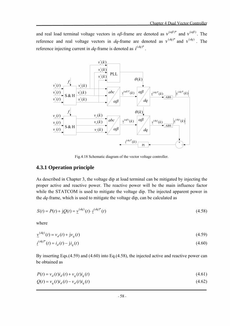
Chapter 4 Dual Vector Controller
- 58 -
and real load terminal voltage vectors in αβ-frame are denoted as *)(αβv and )(αβv . The reference and real voltage vectors in dq-frame are denoted as *)(dqv and )(dqv . The reference injecting current in dq-frame is denoted as . *)(dqi
PI
)(tva
)(tvb
)(tvc
)(kva
)(kvb
)(kvc
abc
αβ
abc
αβ
)()( kv αβ
)(* tva
)(* tvb
)(* tvc
H&S
H&S
)(kθ
αβ
αβ
dq
dq
sf
sf
)(* kva
)(* kvb
)(* kvc
PLL
)(kθ
)(* kva
)(* kvc
)(* kvb
)(*)( kv αβ
+-
)(*)( kv dq
)()( kv dq
)(*)( ki dq
ABS
ABS
)(*)( kv dq
)()( kv dq
Fig.4.18 Schematic diagram of the vector voltage controller. 4.3.1 Operation principle As described in Chapter 3, the voltage dip at load terminal can be mitigated by injecting the proper active and reactive power. The reactive power will be the main influence factor while the STATCOM is used to mitigate the voltage dip. The injected apparent power in the dq-frame, which is used to mitigate the voltage dip, can be calculated as
)()()(j)()( *)()( titvtQtPtS dqdq ⋅=+= (4.58) where
)(j)()()( tvtvtv qddq += (4.59)
)(j)()(*)( tititi qddq −= (4.60)
By inserting Eqs.(4.59) and (4.60) into Eq.(4.58), the injected active and reactive power can be obtained as
)()()()()( titvtitvtP qqdd += (4.61) )()()()()( titvtitvtQ qddq −= (4.62)
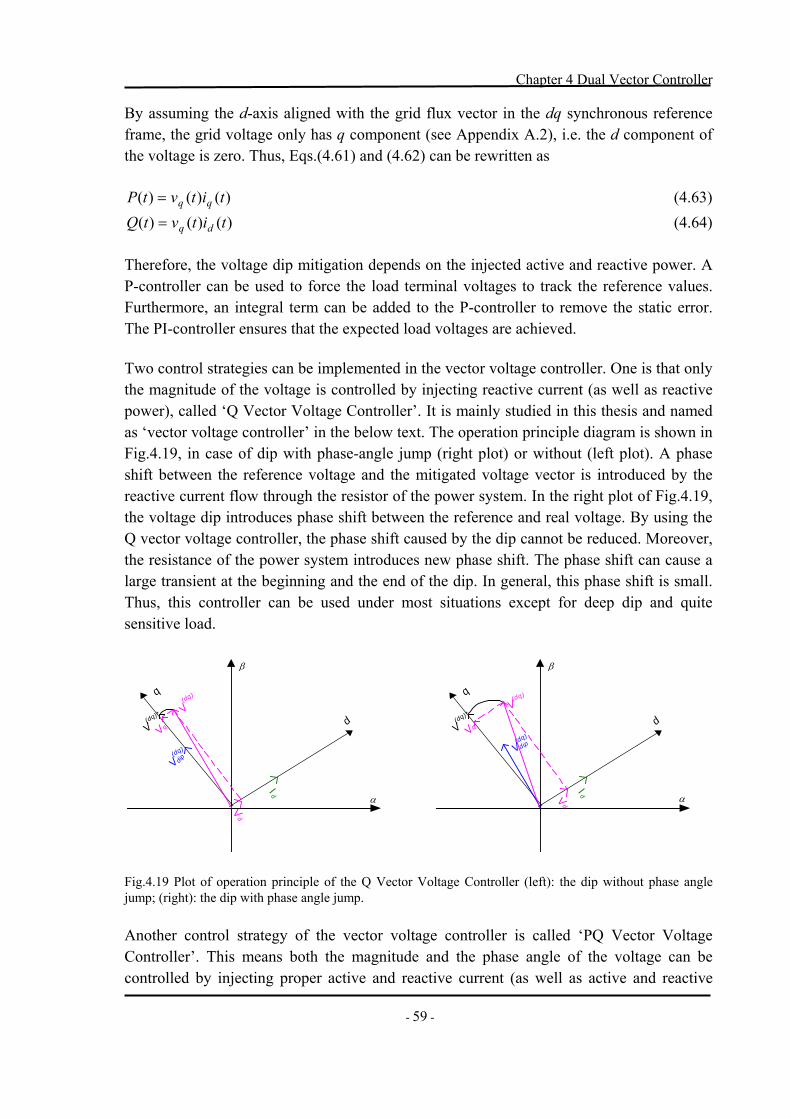
Chapter 4 Dual Vector Controller
- 59 -
By assuming the d-axis aligned with the grid flux vector in the dq synchronous reference frame, the grid voltage only has q component (see Appendix A.2), i.e. the d component of the voltage is zero. Thus, Eqs.(4.61) and (4.62) can be rewritten as
)()()( titvtP qq= (4.63) )()()( titvtQ dq= (4.64)
Therefore, the voltage dip mitigation depends on the injected active and reactive power. A P-controller can be used to force the load terminal voltages to track the reference values. Furthermore, an integral term can be added to the P-controller to remove the static error. The PI-controller ensures that the expected load voltages are achieved. Two control strategies can be implemented in the vector voltage controller. One is that only the magnitude of the voltage is controlled by injecting reactive current (as well as reactive power), called ‘Q Vector Voltage Controller’. It is mainly studied in this thesis and named as ‘vector voltage controller’ in the below text. The operation principle diagram is shown in Fig.4.19, in case of dip with phase-angle jump (right plot) or without (left plot). A phase shift between the reference voltage and the mitigated voltage vector is introduced by the reactive current flow through the resistor of the power system. In the right plot of Fig.4.19, the voltage dip introduces phase shift between the reference and real voltage. By using the Q vector voltage controller, the phase shift caused by the dip cannot be reduced. Moreover, the resistance of the power system introduces new phase shift. The phase shift can cause a large transient at the beginning and the end of the dip. In general, this phase shift is small. Thus, this controller can be used under most situations except for deep dip and quite sensitive load.
α
β
d
q
V(dq)*
Vdip
Id
(dq)
V(dq)
Vq
Vd
α
β
d
q
V(dq)*
V dip
Id
(dq)
V
(dq)
Vq
Vd
Fig.4.19 Plot of operation principle of the Q Vector Voltage Controller (left): the dip without phase angle jump; (right): the dip with phase angle jump. Another control strategy of the vector voltage controller is called ‘PQ Vector Voltage Controller’. This means both the magnitude and the phase angle of the voltage can be controlled by injecting proper active and reactive current (as well as active and reactive
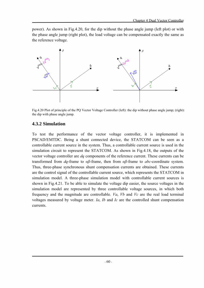
Chapter 4 Dual Vector Controller
- 60 -
power). As shown in Fig.4.20, for the dip without the phase angle jump (left plot) or with the phase angle jump (right plot), the load voltage can be compensated exactly the same as the reference voltage.
α
β
d
q
V(dq)*
Vdip
Id
(dq)
V(dq)
()
Iq
α
β
d
q
V(dq)*
Vdip
Id
(dq)
V
(dq)
()
I q
Fig.4.20 Plot of principle of the PQ Vector Voltage Controller (left): the dip without phase angle jump; (right): the dip with phase angle jump. 4.3.2 Simulation To test the performance of the vector voltage controller, it is implemented in PSCAD/EMTDC. Being a shunt connected device, the STATCOM can be seen as a controllable current source in the system. Thus, a controllable current source is used in the simulation circuit to represent the STATCOM. As shown in Fig.4.18, the outputs of the vector voltage controller are dq components of the reference current. These currents can be transformed from dq-frame to αβ-frame, then from αβ-frame to abc-coordinate system. Thus, three-phase synchronous shunt compensation currents are obtained. These currents are the control signal of the controllable current source, which represents the STATCOM in simulation model. A three-phase simulation model with controllable current sources is shown in Fig.4.21. To be able to simulate the voltage dip easier, the source voltages in the simulation model are represented by three controllable voltage sources, in which both frequency and the magnitude are controllable. Va, Vb and Vc are the real load terminal voltages measured by voltage meter. Ia, Ib and Ic are the controlled shunt compensation currents.
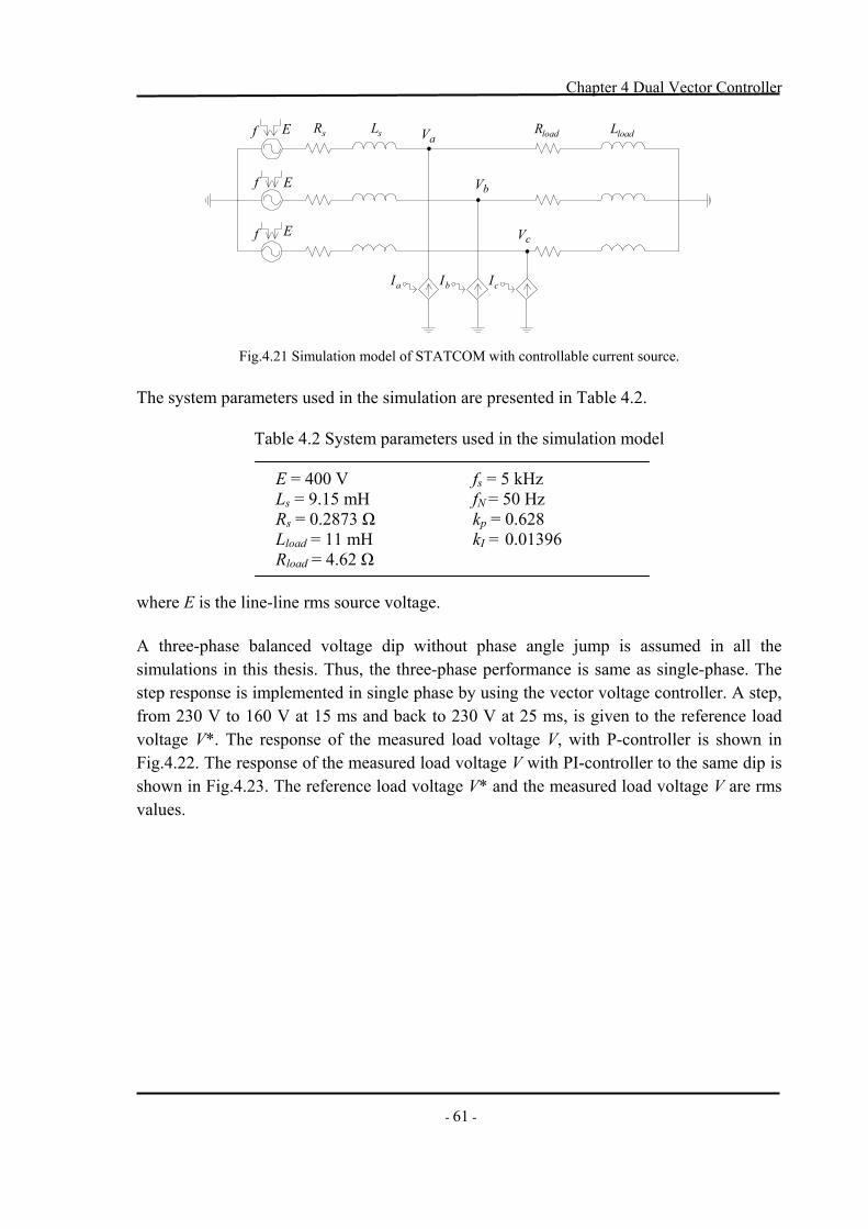
Chapter 4 Dual Vector Controller
- 61 -
aV
f E
loadR loadLsR sLf E
aI bI cI
f E
bV
cV
Fig.4.21 Simulation model of STATCOM with controllable current source.
The system parameters used in the simulation are presented in Table 4.2.
Table 4.2 System parameters used in the simulation model
E = 400 V fs = 5 kHz Ls = 9.15 mH fN = 50 Hz Rs = 0.2873 Ω kp = 0.628 Lload = 11 mH kI = 0.01396 Rload = 4.62 Ω
where E is the line-line rms source voltage. A three-phase balanced voltage dip without phase angle jump is assumed in all the simulations in this thesis. Thus, the three-phase performance is same as single-phase. The step response is implemented in single phase by using the vector voltage controller. A step, from 230 V to 160 V at 15 ms and back to 230 V at 25 ms, is given to the reference load voltage V*. The response of the measured load voltage V, with P-controller is shown in Fig.4.22. The response of the measured load voltage V with PI-controller to the same dip is shown in Fig.4.23. The reference load voltage V* and the measured load voltage V are rms values.
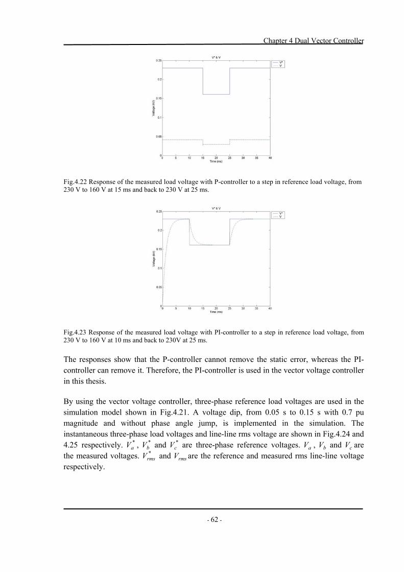
Chapter 4 Dual Vector Controller
- 62 -
Fig.4.22 Response of the measured load voltage with P-controller to a step in reference load voltage, from 230 V to 160 V at 15 ms and back to 230 V at 25 ms.
Fig.4.23 Response of the measured load voltage with PI-controller to a step in reference load voltage, from 230 V to 160 V at 10 ms and back to 230V at 25 ms. The responses show that the P-controller cannot remove the static error, whereas the PI-controller can remove it. Therefore, the PI-controller is used in the vector voltage controller in this thesis. By using the vector voltage controller, three-phase reference load voltages are used in the simulation model shown in Fig.4.21. A voltage dip, from 0.05 s to 0.15 s with 0.7 pu magnitude and without phase angle jump, is implemented in the simulation. The instantaneous three-phase load voltages and line-line rms voltage are shown in Fig.4.24 and 4.25 respectively. , and are three-phase reference voltages. , and are the measured voltages. and are the reference and measured rms line-line voltage respectively.
*aV *
bV *cV aV bV cV
*rmsV rmsV
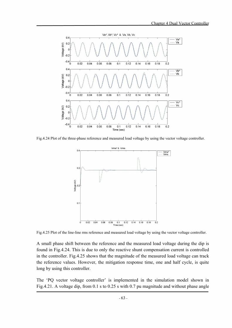
Chapter 4 Dual Vector Controller
- 63 -
Fig.4.24 Plot of the three-phase reference and measured load voltage by using the vector voltage controller.
Fig.4.25 Plot of the line-line rms reference and measured load voltage by using the vector voltage controller.
A small phase shift between the reference and the measured load voltage during the dip is found in Fig.4.24. This is due to only the reactive shunt compensation current is controlled in the controller. Fig.4.25 shows that the magnitude of the measured load voltage can track the reference values. However, the mitigation response time, one and half cycle, is quite long by using this controller. The ‘PQ vector voltage controller’ is implemented in the simulation model shown in Fig.4.21. A voltage dip, from 0.1 s to 0.25 s with 0.7 pu magnitude and without phase angle

Chapter 4 Dual Vector Controller
- 64 -
jump, is implemented in the simulation. The instantaneous three-phase load voltages and line-line rms voltage are shown in Fig.4.26 and 4.27 respectively.
Fig.4.26 Plot of three-phase reference and measured load voltage by using the ‘PQ vector voltage controller’.
Fig.4.27 Plot of the line-line rms reference and measured load voltage by using the ‘PQ vector voltage controller’. Figure 4.26 and 4.27 show that the measured load voltage, both magnitude and phase angle, can track the reference value by using the ‘PQ vector voltage controller’. This is due to both the active and reactive shunt compensation currents are controlled in this controller. The mitigation response time of this controller is also very long.
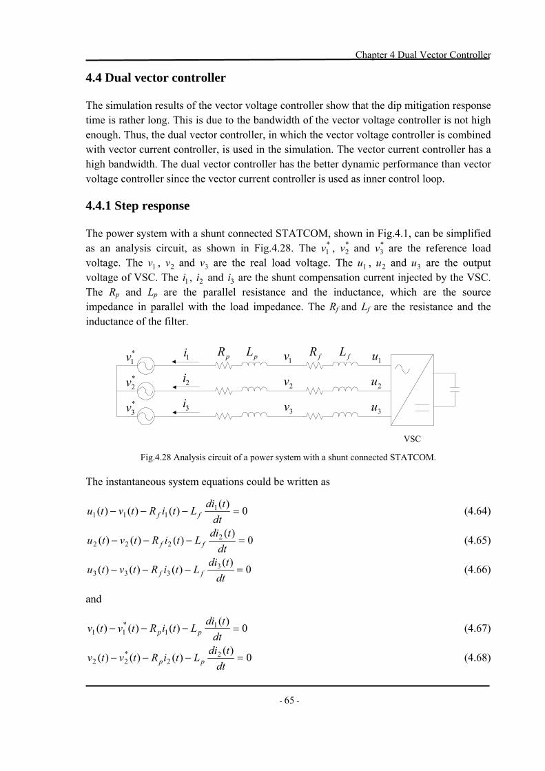
Chapter 4 Dual Vector Controller
- 65 -
4.4 Dual vector controller The simulation results of the vector voltage controller show that the dip mitigation response time is rather long. This is due to the bandwidth of the vector voltage controller is not high enough. Thus, the dual vector controller, in which the vector voltage controller is combined with vector current controller, is used in the simulation. The vector current controller has a high bandwidth. The dual vector controller has the better dynamic performance than vector voltage controller since the vector current controller is used as inner control loop. 4.4.1 Step response The power system with a shunt connected STATCOM, shown in Fig.4.1, can be simplified as an analysis circuit, as shown in Fig.4.28. The , and are the reference load voltage. The , and are the real load voltage. The , and are the output voltage of VSC. The , and are the shunt compensation current injected by the VSC. The R
*1v *
2v *3v
1v 2v 3v 1u 2u 3u1i 2i 3i
p and Lp are the parallel resistance and the inductance, which are the source impedance in parallel with the load impedance. The Rf and Lf are the resistance and the inductance of the filter.
*1v*2v*3v
1i
2i
3i
pLpR fR fL1v
2v
3v
1u
2u
3u
VSC
Fig.4.28 Analysis circuit of a power system with a shunt connected STATCOM. The instantaneous system equations could be written as
0)()()()( 1111 =−−−
dttdiLtiRtvtu ff (4.64)
0)()()()( 2222 =−−−
dttdiLtiRtvtu ff (4.65)
0)(
)()()( 3333 =−−−
dttdi
LtiRtvtu ff (4.66) and
0)()()()( 11
*11 =−−−
dttdiLtiRtvtv pp (4.67)
0)()()()( 22
*22 =−−−
dttdiLtiRtvtv pp (4.68)

Chapter 4 Dual Vector Controller
- 66 -
0)(
)()()( 33
*33 =−−−
dttdi
LtiRtvtv pp (4.69)
As the three-phase system could be transferred to αβ system, Eqs.(4.64) to (4.69) can be written in αβ vector notation as
0)()()( )()()()( )( =−−− tidtdLtiRt ffvtu αβαβαβαβ (4.70)
0)()()( )()()(*)( )( =−−− tidtdLtiRt ppvtv αβαβαβαβ (4.71)
where
)(j)()()( tututu βααβ += (4.72)
)(j)()()( tvtvtv βααβ += (4.73)
)(j)()()( tititi βααβ += (4.74)
)(j)( **)()(* tvtvtv βααβ += (4.75)
By inserting Eq.(4.71) into Eq.(4.70), the below equations can be derived
)(*)(*)(* * tvCtuBtiAv αααα ++= (4.76)
)(*)(*)(* * tvCtuBtiAv ββββ ++= (4.77)
where
fp
fpfp
LLRLLR
A+
−= (4.78)
fp
p
LLL
B+
= (4.79)
fp
f
LLL
C+
= (4.80)
The system equations also can be written as
0)()()()()()( 11
*11 =+−+−−
dttdiLLtiRRtvtu pfpf (4.81)
0)()()()()()( 22
*22 =+−+−−
dttdiLLtiRRtvtu pfpf (4.82)
0)(
)()()()()( 33
*33 =+−+−−
dttdi
LLtiRRtvtu pfpf (4.83)
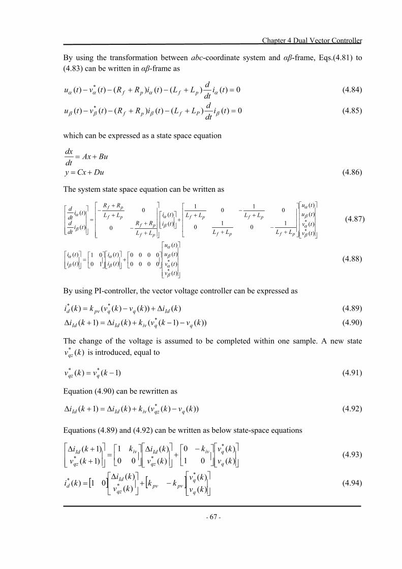
Chapter 4 Dual Vector Controller
- 67 -
By using the transformation between abc-coordinate system and αβ-frame, Eqs.(4.81) to (4.83) can be written in αβ-frame as
0)()()()()()( * =+−+−− tidtdLLtiRRtvtu pfpf αααα (4.84)
0)()()()()()( * =+−+−− tidtdLLtiRRtvtu Pfpf ββββ (4.85)
which can be expressed as a state space equation
BuAxdtdx
+=
DuCxy += (4.86) The system state space equation can be written as
⎥⎥⎥⎥⎥
⎦
⎤
⎢⎢⎢⎢⎢
⎣
⎡
⎥⎥⎥⎥
⎦
⎤
⎢⎢⎢⎢
⎣
⎡
+−
+
+−
++
⎥⎥⎦
⎤
⎢⎢⎣
⎡
⎥⎥⎥⎥⎥
⎦
⎤
⎢⎢⎢⎢⎢
⎣
⎡
+
+−
+
+−
=
⎥⎥⎥⎥
⎦
⎤
⎢⎢⎢⎢
⎣
⎡
)()()()(
1010
0101
)()(
0
0
)(
)(
*
*
tvtvtutu
LLLL
LLLLtiti
LLRR
LLRR
tidtd
tidtd
pfpf
pfpf
pf
pf
pf
pf
β
α
β
α
β
α
β
α (4.87)
⎥⎥⎥⎥⎥
⎦
⎤
⎢⎢⎢⎢⎢
⎣
⎡
⎥⎦
⎤⎢⎣
⎡+
⎥⎥⎦
⎤
⎢⎢⎣
⎡⎥⎦
⎤⎢⎣
⎡=
⎥⎥⎦
⎤
⎢⎢⎣
⎡
)()()()(
00000000
)()(
1001
)()(
*
*
tvtvtutu
titi
titi
β
α
β
α
β
α
β
α (4.88)
By using PI-controller, the vector voltage controller can be expressed as
)())()(()( ** kikvkvkki Idqqpvd ∆+−= (4.89)
))()1(()()1( * kvkvkkiki qqivIdId −−+∆=+∆ (4.90) The change of the voltage is assumed to be completed within one sample. A new state
is introduced, equal to )(* kvqz
)1()( ** −= kvkv qqz (4.91)
Equation (4.90) can be rewritten as
))()(()()1( * kvkvkkiki qqzivIdId −+∆=+∆ (4.92) Equations (4.89) and (4.92) can be written as below state-space equations
⎥⎥⎦
⎤
⎢⎢⎣
⎡⎥⎦
⎤⎢⎣
⎡ −+
⎥⎥⎦
⎤
⎢⎢⎣
⎡∆⎥⎦
⎤⎢⎣
⎡=
⎥⎥⎦
⎤
⎢⎢⎣
⎡
++∆
)()(
010
)()(
001
)1()1( *
** kvkvk
kvkik
kvki
q
qiv
qz
Idiv
qz
Id (4.93)
[ ] [ ]⎥⎥⎦
⎤
⎢⎢⎣
⎡−+⎥
⎦
⎤⎢⎣
⎡∆=
)()(
)()(
01)(*
**
kvkv
kkkvki
kiq
qpvpv
qz
Idd (4.94)
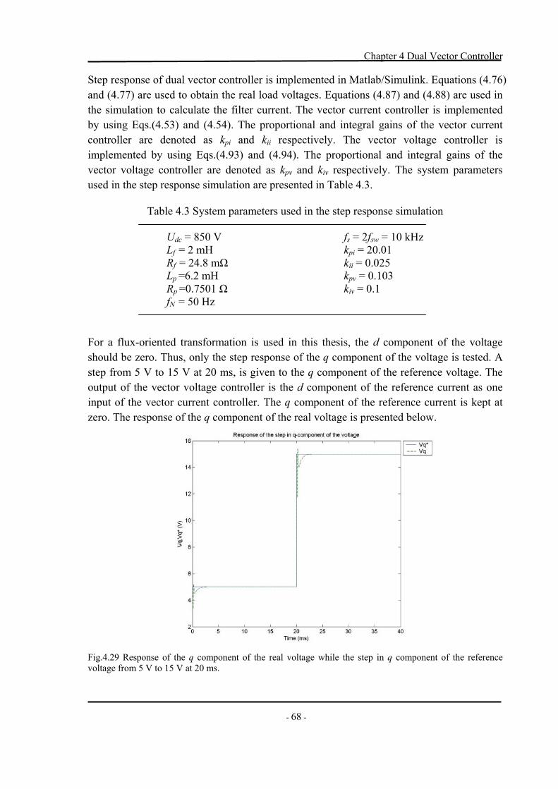
Chapter 4 Dual Vector Controller
- 68 -
Step response of dual vector controller is implemented in Matlab/Simulink. Equations (4.76) and (4.77) are used to obtain the real load voltages. Equations (4.87) and (4.88) are used in the simulation to calculate the filter current. The vector current controller is implemented by using Eqs.(4.53) and (4.54). The proportional and integral gains of the vector current controller are denoted as kpi and kii respectively. The vector voltage controller is implemented by using Eqs.(4.93) and (4.94). The proportional and integral gains of the vector voltage controller are denoted as kpv and kiv respectively. The system parameters used in the step response simulation are presented in Table 4.3.
Table 4.3 System parameters used in the step response simulation
Udc = 850 V fs = 2fsw = 10 kHz Lf = 2 mH kpi = 20.01 Rf = 24.8 mΩ kii = 0.025 Lp =6.2 mH kpv = 0.103 Rp =0.7501 Ω kiv = 0.1 fN = 50 Hz
For a flux-oriented transformation is used in this thesis, the d component of the voltage should be zero. Thus, only the step response of the q component of the voltage is tested. A step from 5 V to 15 V at 20 ms, is given to the q component of the reference voltage. The output of the vector voltage controller is the d component of the reference current as one input of the vector current controller. The q component of the reference current is kept at zero. The response of the q component of the real voltage is presented below.
Fig.4.29 Response of the q component of the real voltage while the step in q component of the reference voltage from 5 V to 15 V at 20 ms.

Chapter 4 Dual Vector Controller
- 69 -
The real voltage can track the reference voltage and the response time is short. For the dual vector controller, the gain of the vector voltage controller should be much smaller than the vector current controller. Otherwise, this controller is unstable. This is due to the fact that the load voltage is considered as constant value in the vector current controller and the filter current is considered as constant value in the vector voltage controller. In case these assumptions cannot be met, the controller cannot work anymore.
4.4.2 Simulation (PSCAD/EMTDC) By using the dual vector controller, a three-phase power system with shunt connected STATCOM is also simulated in PSCAD/EMTDC. The three-phase VSC is represented by three controllable voltage sources [16]. The three-phase simulation model is shown in Fig.4.30. In order to simulate the voltage dip easier, the source voltages in the simulation model are represented by three controllable voltage sources. Va, Vb and Vc are the real load voltages measured by voltage meter. Uaref, Ubref and Ucref are the control signals of the controllable voltage source. These signals come from the output of the vector current controller. A filter is connected between the system and the VSC for each phase since the vector current controller is used in this model.
aV
f E
loadR loadLsR sLf E
f E
bV
cV
crefU
+−
+−
+−
brefU
arefU filterR
filterL
aI bI cI
Fig.4.30 Simulation model of STATCOM with controllable voltage sources.
The system parameters used in the simulation are presented in Table 4.4.
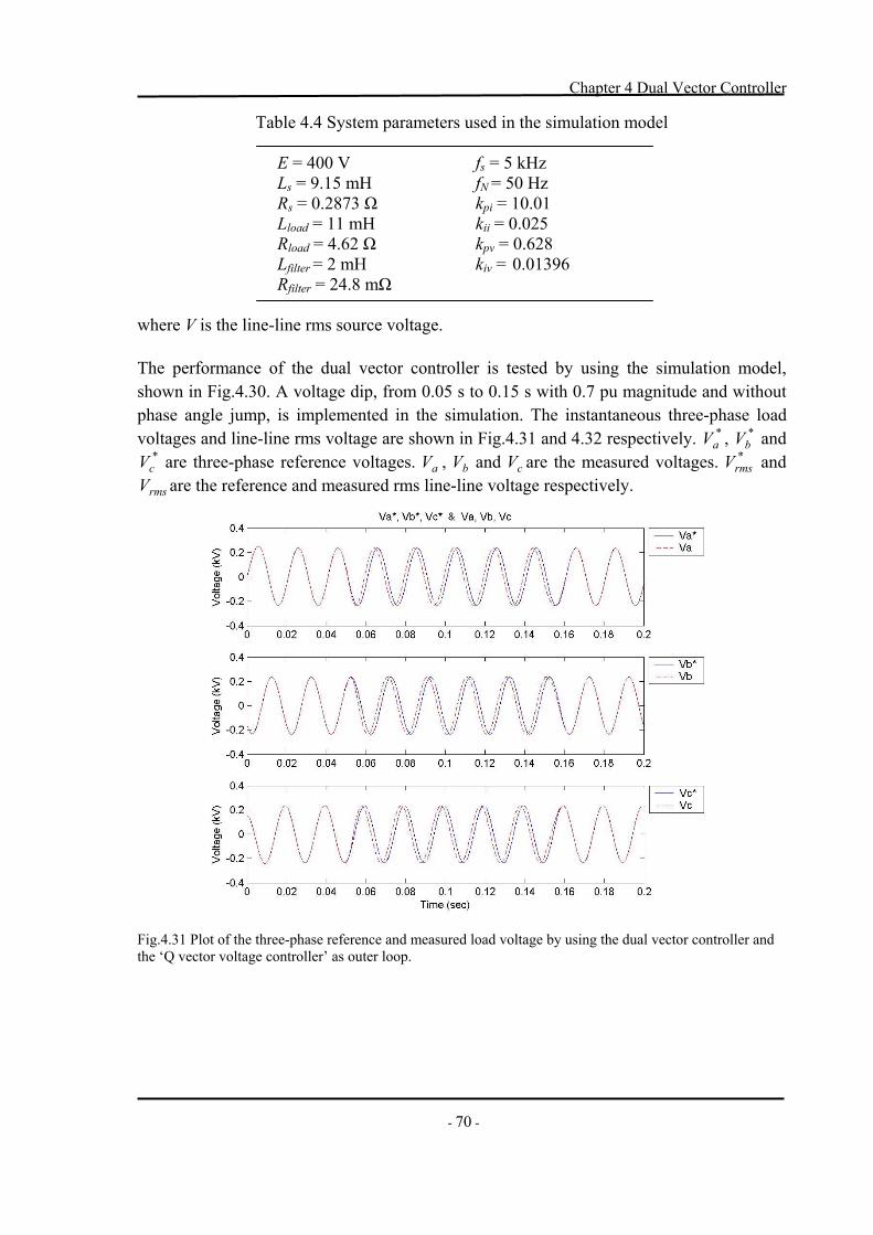
Chapter 4 Dual Vector Controller
- 70 -
Table 4.4 System parameters used in the simulation model
E = 400 V fs = 5 kHz Ls = 9.15 mH fN = 50 Hz Rs = 0.2873 Ω kpi = 10.01 Lload = 11 mH kii = 0.025 Rload = 4.62 Ω kpv = 0.628 Lfilter = 2 mH kiv = 0.01396 Rfilter = 24.8 mΩ
where V is the line-line rms source voltage. The performance of the dual vector controller is tested by using the simulation model, shown in Fig.4.30. A voltage dip, from 0.05 s to 0.15 s with 0.7 pu magnitude and without phase angle jump, is implemented in the simulation. The instantaneous three-phase load voltages and line-line rms voltage are shown in Fig.4.31 and 4.32 respectively. , and
are three-phase reference voltages. , and are the measured voltages. and are the reference and measured rms line-line voltage respectively.
*aV *
bV*
cV aV bV cV *rmsV
rmsV
Fig.4.31 Plot of the three-phase reference and measured load voltage by using the dual vector controller and the ‘Q vector voltage controller’ as outer loop.
Chapter 4 Dual Vector Controller
- 71 -
Fig.4.32 Plot of the line-line rms reference and measured load voltage by using the dual vector controller and the ‘Q vector voltage controller’ as outer loop. There is small phase shift between the reference and the real load voltage during the dip in Fig.4.31. This is due to only the reactive current is controlled in this controller. The magnitude of the reference and the real voltages are exactly same during the dip (see Fig.4.32). Comparing Fig.4.31 and 4.32 to Fig.4.24 and 4.25, the dual vector controller has faster response ability. The voltage dip can be mitigated within 5 ms by using the dual vector controller. This is fast response. In additional, the dual vector controller, in which the ‘PQ vector voltage controller’ is used as the outer loop, is also tested by using the simulation model shown in Fig.4.30. A voltage dip, from 0.1 s to 0.2 s with 0.7 pu magnitude and without phase angle jump, is implemented in the simulation. The instantaneous three-phase load voltages and line-line rms voltage are shown in Fig.4.33 and 4.34 respectively.
Chapter 4 Dual Vector Controller
- 72 -
Fig.4.33 Plot of the three-phase reference and measured load voltage by using the dual vector controller and the ‘PQ vector voltage controller’ as outer loop.
Fig.4.34 Plot of the line-line rms reference and measured load voltage by using the dual vector controller and the ‘PQ vector voltage controller’ as outer loop. No phase shift between the reference and the real load voltage during the dip is found in Fig.4.33. The magnitude and the phase angle are exactly same for the two voltages during the dip. However, the dip mitigation response time is longer than the case by using the ‘Q vector voltage controller’ as the outer loop of the dual vector controller. From now on, only the dual vector controller, in which the ‘Q vector voltage controller’ is used as outer control loop, is studied. To verify the performance of the dual vector controller, several cases are studied by using the same controller parameters.
Chapter 4 Dual Vector Controller
- 73 -
Variation of the dip magnitude Several dip magnitudes, 0.9 pu, 0.7 pu, 0.5 pu and 0.2 pu, are selected to test the performance of the controller. The voltage dip can be mitigated completely. The instantaneous three-phase load voltages and line-line rms voltage with the dip, which starts from 0.05 s to 0.15 s with magnitude 0.2 pu, are shown in Fig.4.35 and 4.36.
Fig.4.35 Plot of three-phase reference and measured load voltage with dip magnitude 0.2 pu.
Fig.4.36 Plot of line-line rms reference and measured load voltage with dip magnitude 0.2 pu.
Comparing the Fig.4.35 to the Fig.4.31, the larger phase shift between the reference and the real voltage during the dip is found in Fig.4.35. This is due to the shunt compensation current increase while the dip magnitude decreases. Thus the voltage caused by the shunt compensation current flow through the resistance of the system increases as the dip

Chapter 4 Dual Vector Controller
- 74 -
magnitude decreases. Consequently, the phase shift introduced by this voltage increases while the dip magnitude decreases. Comparing the Fig.4.36 with the Fig.4.32, the larger transients at the beginning and the end of the dip are found in Fig.4.36. This is also caused by the larger shunt compensation current for deeper dip. Variation of the characteristic of the system impedance The same system parameters, as shown in Table 4.4, are used in simulation except for the resistances of the source and the load are set as zero. The instantaneous three-phase load voltages and line-line rms voltage with the dip, which starts from 0.1 s to 0.2 s with magnitude 0.7 pu, are shown in Fig.4.37 and 4.38.
Fig.4.37 Plot of three-phase reference and measured load voltage with pure inductive source and the load.
Fig.4.38 Plot of line-line rms reference and measured load voltage with pure inductive source and load.
Chapter 4 Dual Vector Controller
- 75 -
The Fig.4.37 shows that there is no phase shift between the reference and the real load voltage during the dip since there is no resistance in the power system. For the voltage dip without phase angle jump, the resistance of the power system is the factor that introduces the phase shift of the compensated load voltage during the dip. Another case, which can verify this theory, is tested below. The system parameters shown in Table 4.4 are used in the simulation except for the resistance of the source is set as zero. The difference with the above case is the resistance of the load is not zero in this case. The instantaneous three-phase load voltages and line-line rms voltage with the dip, which starts from 0.1 s to 0.2 s with magnitude 0.7 pu, are shown in Fig.4.39 and 4.40.
Fig.4.39 Plot of three-phase reference and measured load voltage with pure inductive source.
Fig.4.40 Plot of line-line rms reference and measured load voltage with pure inductive source.

Chapter 4 Dual Vector Controller
- 76 -
Due to the load resistance is not zero, the small phase shift between the reference and the real load voltage during the dip is found in Fig.4.39. Variation of the system impedance Based on the system parameters presented in the Table 4.4, the half load impedance (Lload = 5.5 mH, Rload = 2.31 Ω), double load impedance (Lload = 22 mH, Rload = 9.24 Ω), half source impedance (Ls = 4.575 mH, Rs = 0.14365 Ω) and double source impedance (Ls = 18.3 mH, Rs = 0.5746 Ω) are used in the simulation respectively. A voltage dip, which starts at 0.1 s and stops at 0.2 s with magnitude 0.7 pu, is implemented in the simulation. The simulation results for each case are presented in Fig.4.41 to 4.48.
Fig.4.41 Plot of three-phase reference and measured load voltage for half load impedance.
Fig.4.42 Plot of line-line rms reference and measured load voltage for half load impedance.

Chapter 4 Dual Vector Controller
- 77 -
Fig.4.43 Plot of three-phase reference and measured load voltage for double load impedance.
Fig.4.44 Plot of line-line rms reference and measured load voltage for double load impedance.
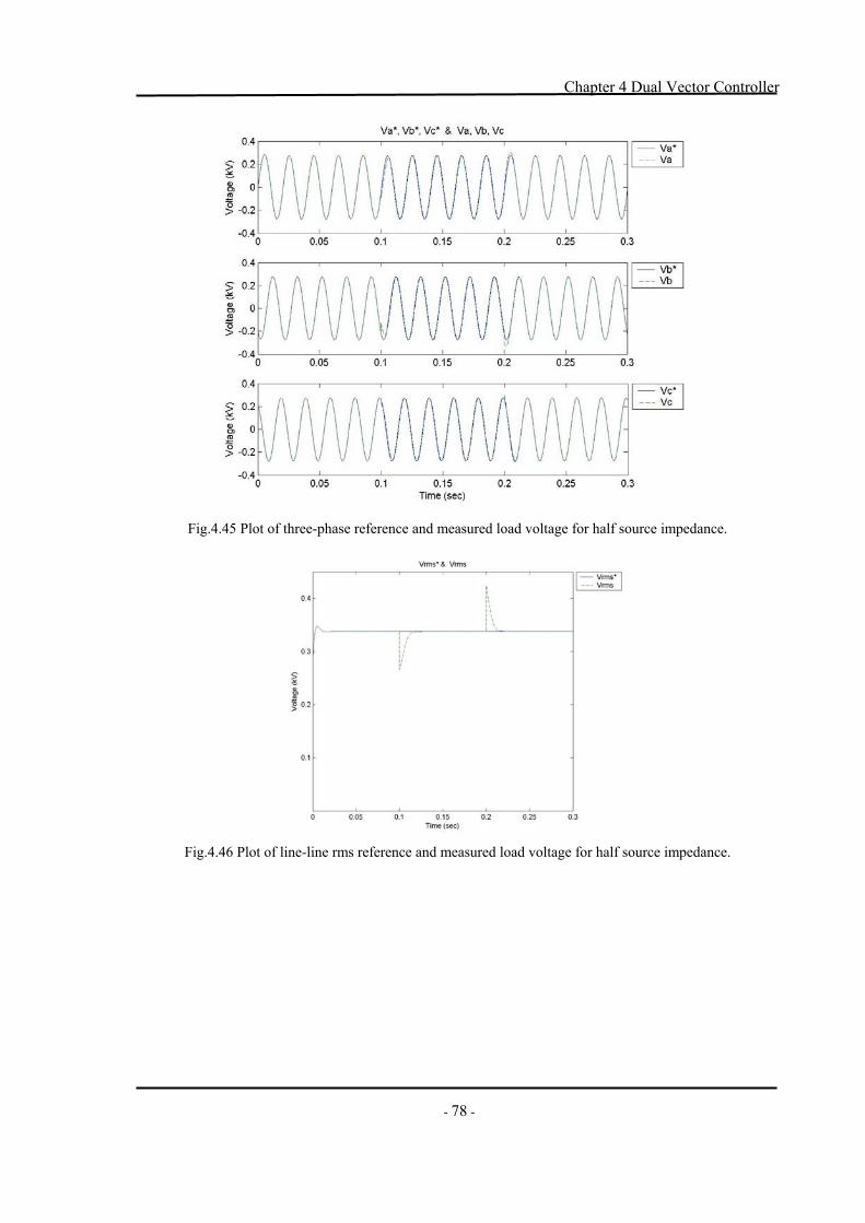
Chapter 4 Dual Vector Controller
- 78 -
Fig.4.45 Plot of three-phase reference and measured load voltage for half source impedance.
Fig.4.46 Plot of line-line rms reference and measured load voltage for half source impedance.
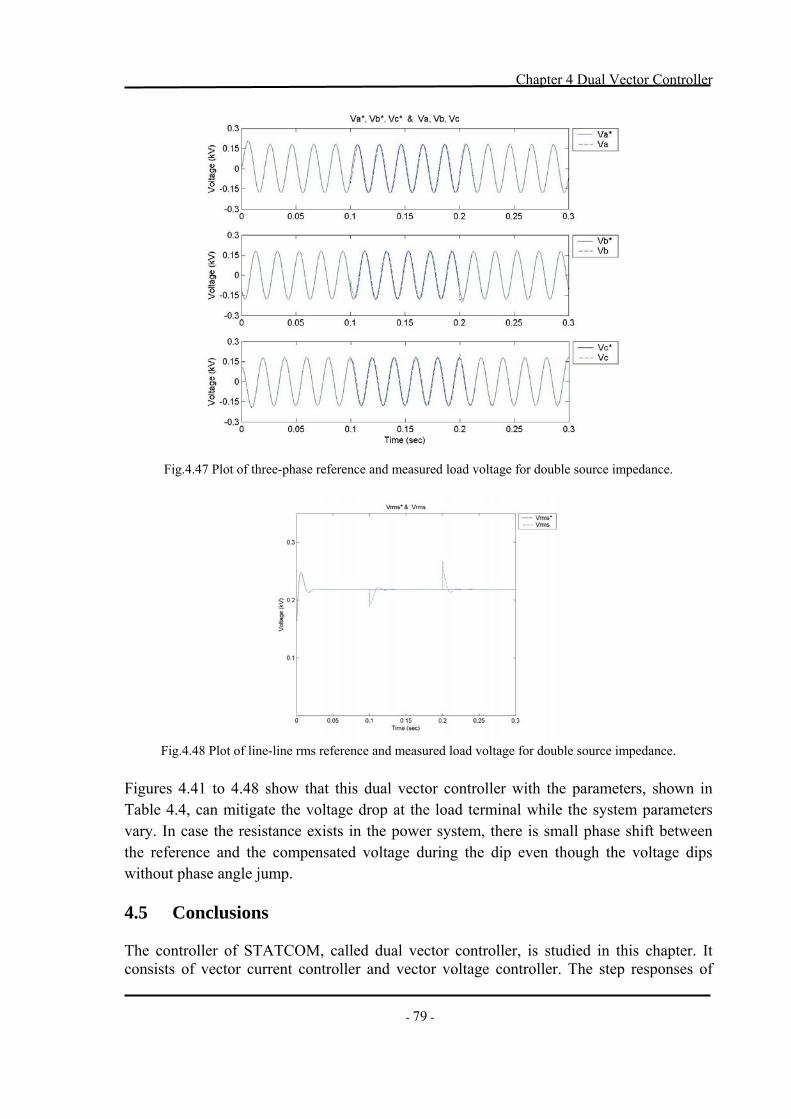
Chapter 4 Dual Vector Controller
- 79 -
Fig.4.47 Plot of three-phase reference and measured load voltage for double source impedance.
Fig.4.48 Plot of line-line rms reference and measured load voltage for double source impedance.
Figures 4.41 to 4.48 show that this dual vector controller with the parameters, shown in Table 4.4, can mitigate the voltage drop at the load terminal while the system parameters vary. In case the resistance exists in the power system, there is small phase shift between the reference and the compensated voltage during the dip even though the voltage dips without phase angle jump. 4.5 Conclusions The controller of STATCOM, called dual vector controller, is studied in this chapter. It consists of vector current controller and vector voltage controller. The step responses of

Chapter 4 Dual Vector Controller
- 80 -
vector current controller with deadbeat gain, vector voltage controller and dual vector controller have been presented. Two three-phase simplified models by using vector voltage controller and dual vector controller are built in PSCAD/EMTDC respectively. The various system parameters also have been tested in the simulation model with dual vector controller. Results show that voltage dip can be mitigated by STATCOM with dual vector controller in 5 ms. This controller can mitigate the voltage dip for various system parameters. Due to reactive power control is used in dual vector controller, there is small phase shift between real and reference voltage during the dip.
Chapter 5 400 V System Simulation
Chapter 5
400 V System Simulation Two simplified simulation models are presented in Chapter 4. One is simplified system model with three controllable current sources representing the STATCOM to test the vector voltage controller. The other one is simplified system model with three controllable voltage sources representing the VSC to test the dual vector controller. The main problem of the two simplified models is that an ideal VSC is assumed in them, i.e. the shunt compensation currents and the output voltages of the VSC are pure sinusoidal wave and without any harmonic content. This is unrealistic. In reality, the PWM technique is implemented in the VSC. Thus, the switching of the VSC introduces harmonics into the output voltages of the converter. As a result, the shunt compensation currents also suffer from these harmonics. To obtain a more realistic simulation model, the model representing the real IGBT valve in PSCAD/EMTDC is used to build a realistic VSC simulation model. The simulation model is presented in section 5.1. The step responses of vector current controller are described in section 5.2. Section 5.3 gives the simulation results for various system parameters. 5.1 Simulation model To attenuate harmonics in the shunt compensation current, generally, a filter is placed between the VSC and the point of the power system, with which the STATCOM is connected. It is shown in Fig.5.1.
Fig.5.1 IGBT simulation model in PSCAD/EMTDC.
The six-pulse forced commutated VSC is used in the simulation model. The three-phase simulation model, with a real three-phase VSC, is shown in Fig.5.2. This model still is an equivalent circuit of power system with STATCOM. In this model, the six switching control signals T1 to T6 come from the outputs of the dual vector controller.
- 81 -

Chapter 5 400 V System Simulation
sR sL loadR loadL
filterR
filterL
dcU
1T
2T
3T
4T
5T
6T
C
aV
bV
cV
aE
bE
cE
Fig.5.2 Three-phase simulation model with real converter. 5.2 Step response To verify the performance of this real converter model, step response simulation is tested in STATCOM model, which is composed of three-phase converter, three L-filters and three voltage sources. The vector current controller is used in this simulation. The system parameters and the vector current controller parameters, used in the simulation, are presented in Table 5.1 and Table 5.2 respectively.
Table 5.1 System parameters used in step response simulation
Source Voltage (line-line rms) 400 V DC-link Voltage 1000 V Filter Resistance 24.8 mΩ Filter Inductance 2 mH Switching Frequency 2.5 kHz Sampling Frequency 5 kHz
Table 5.2 Parameters of vector current controller used in step response simulation
Proportional Gain (kp) 10.01 Integral Constant (ki) 0.0248
A step pulse, where the magnitude varies between 5 A and 15 A, and the pulse width is 0.04 s, is given to the reference reactive current while the reference active current is kept constant at 18 A. The responses of the real active and reactive currents, and , are shown in Fig.5.3.
*di
*qi
di qi
- 82 -
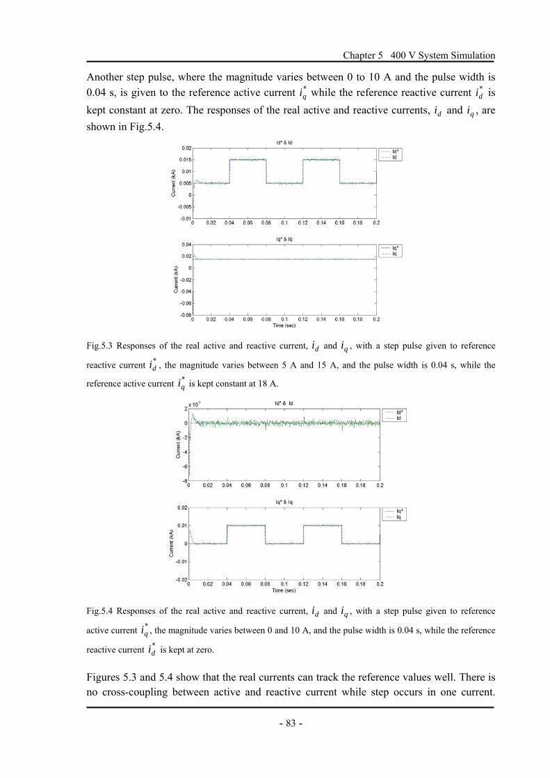
Chapter 5 400 V System Simulation
Another step pulse, where the magnitude varies between 0 to 10 A and the pulse width is 0.04 s, is given to the reference active current while the reference reactive current is kept constant at zero. The responses of the real active and reactive currents, and , are shown in Fig.5.4.
*qi
*di
di qi
Fig.5.3 Responses of the real active and reactive current, and , with a step pulse given to reference
reactive current , the magnitude varies between 5 A and 15 A, and the pulse width is 0.04 s, while the
reference active current is kept constant at 18 A.
di qi*di
*qi
Fig.5.4 Responses of the real active and reactive current, and , with a step pulse given to reference
active current , the magnitude varies between 0 and 10 A, and the pulse width is 0.04 s, while the reference
reactive current is kept at zero.
di qi*qi
*di
Figures 5.3 and 5.4 show that the real currents can track the reference values well. There is no cross-coupling between active and reactive current while step occurs in one current.
- 83 -
Chapter 5 400 V System Simulation
Comparing Figs.5.3 and 5.4 to the Figs.4.8 and 4.9, small oscillations are found in the active and reactive current of Figs.5.3 and 5.4. This is caused by the harmonic content of the current, introduced by the switching devices in the real VSC simulation model. The harmonics mainly occur around the switching frequency and multiple of the switching frequency. Due to the switching frequency is high, e.g. 5 kHz in the simulation, a small filter can be used to filter high frequency harmonics. However, small unavoidable harmonics still exist in the filter current and result in small oscillations in the current. 5.3 Simulation results The simulation model, shown in Fig.5.2, is used to test the performance of the dual vector controller for several cases. A voltage dip, with 0.7 pu magnitude and duration from 0.1 s to 0.2 s, is implemented in all simulations in this chapter. The simulation results are shown below. The system parameters used in the simulation are presented in Table 5.3.
Table 5.3 System parameters used in the simulation
Source Voltage (line-line rms) 400 V DC-link Voltage 1000 V Source Resistance 12.4 mΩ Source Inductance 1.0 mH Load Resistance 3.0 Ω Load Inductance 7.2E-12 H Filter Resistance 24.8 mΩ Filter Inductance 2 mH Switching Frequency 2.5 kHz Sampling Frequency 5 kHz
Due to there are inductances in the simulation circuit, transients occur while the voltage and filter current have step, caused by the dip. These transients also bring the problems of voltage saturation, which is the output voltage of the VSC, into the controller. This problem becomes critical if high gain of the vector current controller is used. Tests show that the overmodulation is found at the end of the dip when the deadbeat gain in the vector current controller is used. Thus, a lower gain is used in the vector current controller instead of the deadbeat gain in this simulation model. Table 5.4 shows the parameters used in dual vector controller with 50% deadbeat gain in vector current controller. Figures 5.3 and 5.4 show the corresponding simulation results.
Table 5.4 Parameters of the dual vector controller with deadbeat gain
Vector Current Controller Vector Voltage Controller Proportional Gain (kp) 5.006 (50% deadbeat gain) 0.62 Integral Constant (ki) 0.01242 0.124
- 84 -

Chapter 5 400 V System Simulation
Fig.5.3 Compensated load voltage by using 50% deadbeat gain in the vector current controller (top) The compensated load voltage in three-phase system (middle) The reference and the compensated load voltage in dq system (bottom) The rms value of the compensated load voltage.
Fig.5.4 Shunt compensation current by using 50% deadbeat gain in the vector current controller (top) The current in three-phase system (middle) The real and reference reactive current (bottom) The real and reference active current.
- 85 -
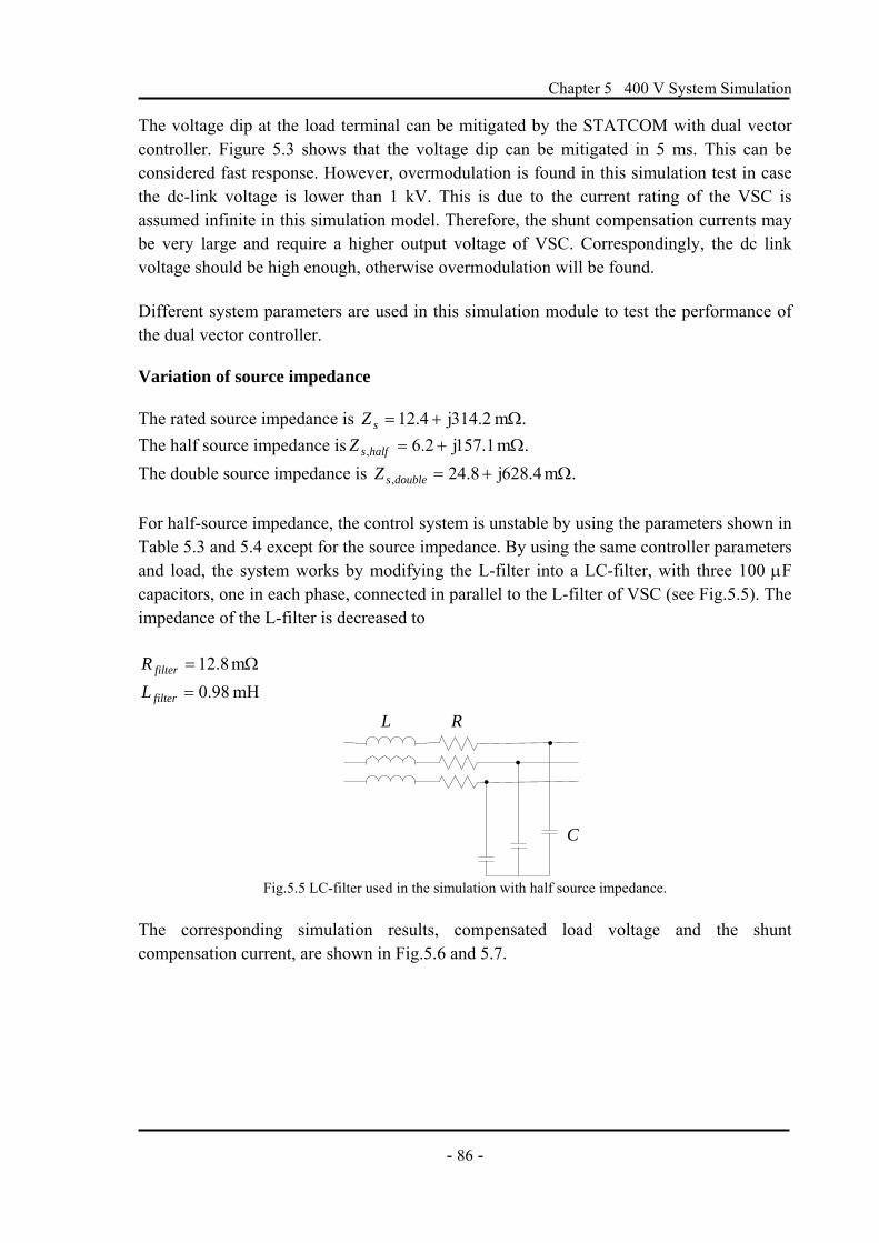
Chapter 5 400 V System Simulation
The voltage dip at the load terminal can be mitigated by the STATCOM with dual vector controller. Figure 5.3 shows that the voltage dip can be mitigated in 5 ms. This can be considered fast response. However, overmodulation is found in this simulation test in case the dc-link voltage is lower than 1 kV. This is due to the current rating of the VSC is assumed infinite in this simulation model. Therefore, the shunt compensation currents may be very large and require a higher output voltage of VSC. Correspondingly, the dc link voltage should be high enough, otherwise overmodulation will be found. Different system parameters are used in this simulation module to test the performance of the dual vector controller. Variation of source impedance The rated source impedance is 2.314j4.12 +=sZ mΩ. The half source impedance is 1.157j2.6, +=halfsZ mΩ. The double source impedance is 4.628j8.24, +=doublesZ mΩ. For half-source impedance, the control system is unstable by using the parameters shown in Table 5.3 and 5.4 except for the source impedance. By using the same controller parameters and load, the system works by modifying the L-filter into a LC-filter, with three 100 µF capacitors, one in each phase, connected in parallel to the L-filter of VSC (see Fig.5.5). The impedance of the L-filter is decreased to
8.12=filterR mΩ 98.0=filterL mH
RL
C
Fig.5.5 LC-filter used in the simulation with half source impedance.
The corresponding simulation results, compensated load voltage and the shunt compensation current, are shown in Fig.5.6 and 5.7.
- 86 -
Chapter 5 400 V System Simulation
Fig.5.6 Compensated load voltage by using LC-filter and with half source impedance (top) The compensated load voltage in three-phase system (middle) The reference and the compensated load voltage in dq system (bottom) The rms value of the compensated load voltage.
Fig.5.7 Shunt compensation current by using LC-filter and with half source impedance (top) The current in three-phase system (middle) The real and reference reactive current (bottom) The real and reference active current.
- 87 -
Chapter 5 400 V System Simulation
The simulation results, compensated load voltage and the shunt compensation current, with double source impedance are presented in Fig.5.8 and 5.9 respectively.
Fig.5.8 Compensated load voltage by using L-filter and with double source impedance (top) The compensated load voltage in three-phase system (middle) The reference and the compensated load voltage in dq system (bottom) The rms value of the compensated load voltage.
Fig.5.9 Shunt compensation current by using LC-filter and with double source impedance (top) The current in three-phase system (middle) The real and reference reactive current (bottom) The real and reference active current.
- 88 -
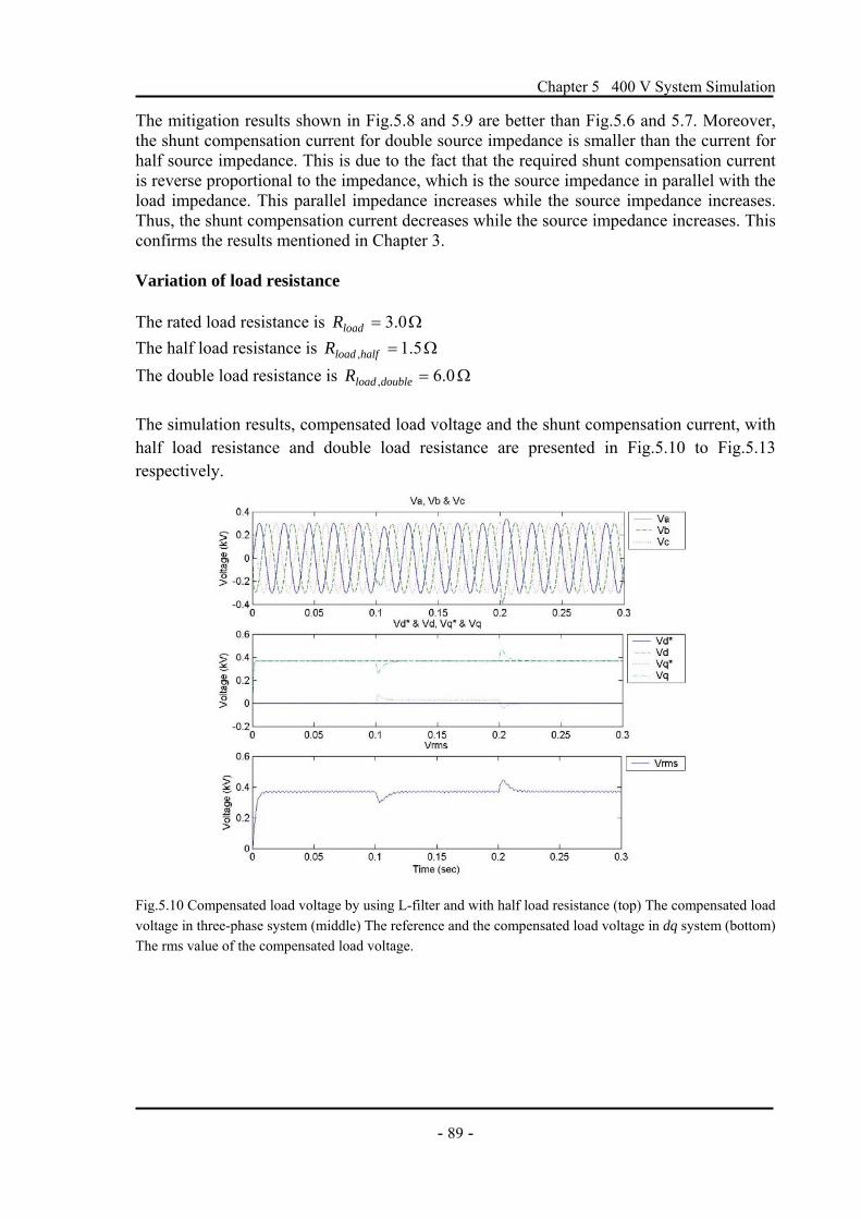
Chapter 5 400 V System Simulation
The mitigation results shown in Fig.5.8 and 5.9 are better than Fig.5.6 and 5.7. Moreover, the shunt compensation current for double source impedance is smaller than the current for half source impedance. This is due to the fact that the required shunt compensation current is reverse proportional to the impedance, which is the source impedance in parallel with the load impedance. This parallel impedance increases while the source impedance increases. Thus, the shunt compensation current decreases while the source impedance increases. This confirms the results mentioned in Chapter 3. Variation of load resistance The rated load resistance is 0.3=loadR Ω The half load resistance is 5.1, =halfloadR Ω The double load resistance is 0.6, =doubleloadR Ω The simulation results, compensated load voltage and the shunt compensation current, with half load resistance and double load resistance are presented in Fig.5.10 to Fig.5.13 respectively.
Fig.5.10 Compensated load voltage by using L-filter and with half load resistance (top) The compensated load voltage in three-phase system (middle) The reference and the compensated load voltage in dq system (bottom) The rms value of the compensated load voltage.
- 89 -
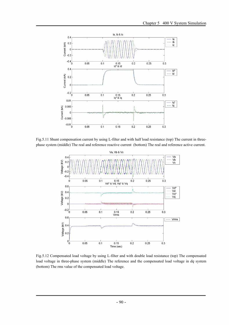
Chapter 5 400 V System Simulation
Fig.5.11 Shunt compensation current by using L-filter and with half load resistance (top) The current in three-phase system (middle) The real and reference reactive current (bottom) The real and reference active current.
Fig.5.12 Compensated load voltage by using L-filter and with double load resistance (top) The compensated load voltage in three-phase system (middle) The reference and the compensated load voltage in dq system (bottom) The rms value of the compensated load voltage.
- 90 -

Chapter 5 400 V System Simulation
Fig.5.13 Shunt compensation current by using L-filter and with double load resistance (top) The current in three-phase system (middle) The real and reference reactive current (bottom) The real and reference active current. As shown in Fig.5.10 to Fig.5.13, the system works better by using the dual vector controller with the parameters presented in Table 5.4 while the load resistance decreases. The compensated load voltage waveform during the dip is distorted slightly and the current ripple is also bigger when the load resistance is increased. This is due to the fact that the load resistance increases, more load current is drawn from the source. The voltage drop caused by the source impedance is larger. Voltage oscillations easier occur at the load terminal during the dip. Due to the load terminal voltage is one input of dual vector controller, the current ripple also occurs in the shunt compensation current. 5.4 Conclusions In this chapter, the actual model of a VSC with IGBT valves has been simulated with PSCAD/EMTDC. The VSC is controlled by the dual vector controller explained in Chapter 4 and is connected to a simple 400 V grid model. The performance has been studied by step responses of vector current controller and three-phase system simulation with various system parameters. Results demonstrated that there are small oscillations in dq component of the shunt compensation current due to the switching ripple of the VSC. It is also shown that the performance of the dual vector controller is sensitive to the variation of the system parameters. The system only can works by modifying the L-filter into a LC-filter when the source impedance decreases to half rated value. The shunt compensation current increases when the source impedance increases or the load resistance increases.
- 91 -
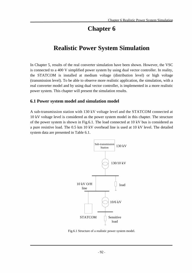
Chapter 6 Realistic Power System Simulation
92
Chapter 6
Realistic Power System Simulation
In Chapter 5, results of the real converter simulation have been shown. However, the VSC is connected to a 400 V simplified power system by using dual vector controller. In reality, the STATCOM is installed at medium voltage (distribution level) or high voltage (transmission level). To be able to observe more realistic application, the simulation, with a real converter model and by using dual vector controller, is implemented in a more realistic power system. This chapter will present the simulation results. 6.1 Power system model and simulation model A sub-transmission station with 130 kV voltage level and the STATCOM connected at 10 kV voltage level is considered as the power system model in this chapter. The structure of the power system is shown in Fig.6.1. The load connected at 10 kV bus is considered as a pure resistive load. The 0.5 km 10 kV overhead line is used at 10 kV level. The detailed system data are presented in Table 6.1.
Sub-transmissionStation
STATCOM
130 kV
130/10 kV
10/6 kV
Sensitiveload
load10 kV O/Hline
Fig.6.1 Structure of a realistic power system model.
- -
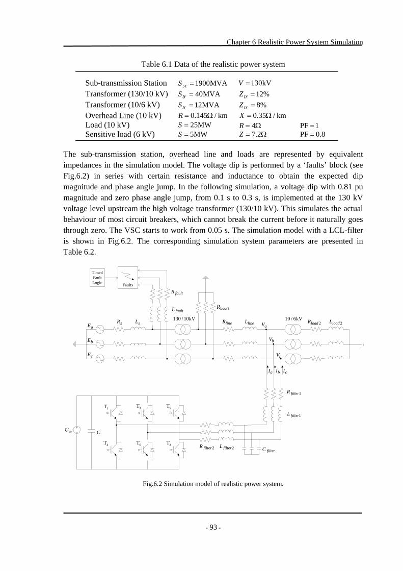
Chapter 6 Realistic Power System Simulation
93
Table 6.1 Data of the realistic power system
Sub-transmission Station MVA1900=scS kV130=V Transformer (130/10 kV) MVA40=trS %12=trZ Transformer (10/6 kV) MVA12=trS %8=trZ Overhead Line (10 kV) km/145.0 Ω=R km/35.0 Ω=X Load (10 kV) MW25=S Ω= 4R 1PF = Sensitive load (6 kV) MW5=S Ω= 2.7Z 8.0PF =
The sub-transmission station, overhead line and loads are represented by equivalent impedances in the simulation model. The voltage dip is performed by a ‘faults’ block (see Fig.6.2) in series with certain resistance and inductance to obtain the expected dip magnitude and phase angle jump. In the following simulation, a voltage dip with 0.81 pu magnitude and zero phase angle jump, from 0.1 s to 0.3 s, is implemented at the 130 kV voltage level upstream the high voltage transformer (130/10 kV). This simulates the actual behaviour of most circuit breakers, which cannot break the current before it naturally goes through zero. The VSC starts to work from 0.05 s. The simulation model with a LCL-filter is shown in Fig.6.2. The corresponding simulation system parameters are presented in Table 6.2.
Faults
TimedFaultLogic
aE
bE
cE
sR sL kV10/130lineR lineL kV6/10
1loadR
2loadR 2loadL
faultR
faultL
aV
bV
cV
dcU
1T
2T
3T
4T
5T
6T
C
1filterR
1filterL
2filterR 2filterLfilterC
aI bI cI
Fig.6.2 Simulation model of realistic power system.
- -

Chapter 6 Realistic Power System Simulation
94
Table 6.2 System parameters used in the simulation model
Source Impedance Ω= 885.0sR mH2.28=sL O/H Line Impedance Ω= 0.01813lineR mH1393.0=lineL Load impedance Ω= 41loadR Sensitive Load Impedance Ω= 76.52loadR mH75.132 =loadL Grid-side Filter Impedance Ω= 0248.01filterR mH7894.01 =filterL VSC-side Filter Impedance Ω= 036.02filterR mH146.12 =filterL Filter Capacitance µF60=filterC DC Voltage kV20=dcU Switching Frequency kHz5.2=swf Sampling Frequency kHz5=sf
The parameters of the dual vector controller are presented in Table 6.3. Since the voltage at the point of connection of the STATCOM is not stiff, the deadbeat gain cannot be used in the controller. A gain equal to 80% of deadbeat has been used in the simulations in this chapter.
Table 6.3 parameters of the dual vector controller
Vector Current Controller Vector Voltage Controller Proportional Gain (kp) 4.598 (80% deadbeat gain) 0.34 Integral Constant (ki) 0.02889 0.113
6.2 Different filter configuration In this realistic power system simulation model, the L-filter, as shown in Fig.5.2, is not suitable any more. It cannot attenuate the harmonics caused by the switching ripples of the VSC in the high-power application. The three-phase 10 kV bus compensated voltages and dq-components of the voltages by using L-filter are presented in Fig.6.3. The parameters of L-filter are same as the VSC-side filter, shown in Table 6.2. As the figure shows, the voltage is distorted during the dip. The voltage at the point of connection of the VSC is weak in this system.
- -
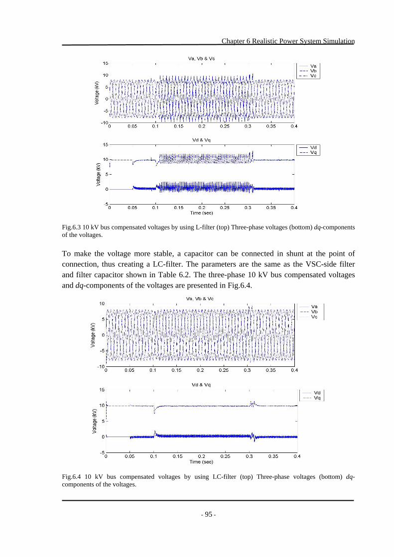
Chapter 6 Realistic Power System Simulation
95
Fig.6.3 10 kV bus compensated voltages by using L-filter (top) Three-phase voltages (bottom) dq-components of the voltages. To make the voltage more stable, a capacitor can be connected in shunt at the point of connection, thus creating a LC-filter. The parameters are the same as the VSC-side filter and filter capacitor shown in Table 6.2. The three-phase 10 kV bus compensated voltages and dq-components of the voltages are presented in Fig.6.4.
Fig.6.4 10 kV bus compensated voltages by using LC-filter (top) Three-phase voltages (bottom) dq- components of the voltages.
- -
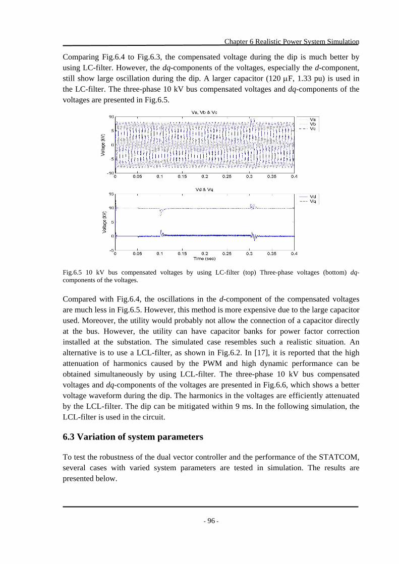
Chapter 6 Realistic Power System Simulation
96
Comparing Fig.6.4 to Fig.6.3, the compensated voltage during the dip is much better by using LC-filter. However, the dq-components of the voltages, especially the d-component, still show large oscillation during the dip. A larger capacitor (120 µF, 1.33 pu) is used in the LC-filter. The three-phase 10 kV bus compensated voltages and dq-components of the voltages are presented in Fig.6.5.
Fig.6.5 10 kV bus compensated voltages by using LC-filter (top) Three-phase voltages (bottom) dq- components of the voltages. Compared with Fig.6.4, the oscillations in the d-component of the compensated voltages are much less in Fig.6.5. However, this method is more expensive due to the large capacitor used. Moreover, the utility would probably not allow the connection of a capacitor directly at the bus. However, the utility can have capacitor banks for power factor correction installed at the substation. The simulated case resembles such a realistic situation. An alternative is to use a LCL-filter, as shown in Fig.6.2. In [17], it is reported that the high attenuation of harmonics caused by the PWM and high dynamic performance can be obtained simultaneously by using LCL-filter. The three-phase 10 kV bus compensated voltages and dq-components of the voltages are presented in Fig.6.6, which shows a better voltage waveform during the dip. The harmonics in the voltages are efficiently attenuated by the LCL-filter. The dip can be mitigated within 9 ms. In the following simulation, the LCL-filter is used in the circuit. 6.3 Variation of system parameters To test the robustness of the dual vector controller and the performance of the STATCOM, several cases with varied system parameters are tested in simulation. The results are presented below.
- -
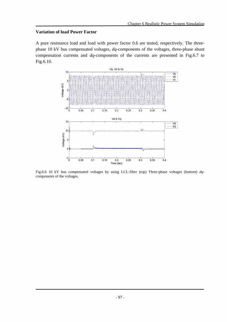
Chapter 6 Realistic Power System Simulation
97
Variation of load Power Factor A pure resistance load and load with power factor 0.6 are tested, respectively. The three-phase 10 kV bus compensated voltages, dq-components of the voltages, three-phase shunt compensation currents and dq-components of the currents are presented in Fig.6.7 to Fig.6.10.
Fig.6.6 10 kV bus compensated voltages by using LCL-filter (top) Three-phase voltages (bottom) dq- components of the voltages.
- -
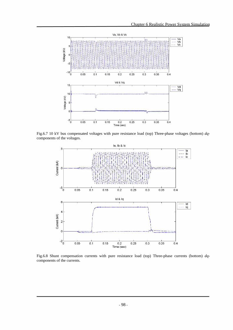
Chapter 6 Realistic Power System Simulation
98
Fig.6.7 10 kV bus compensated voltages with pure resistance load (top) Three-phase voltages (bottom) dq- components of the voltages.
Fig.6.8 Shunt compensation currents with pure resistance load (top) Three-phase currents (bottom) dq- components of the currents.
- -
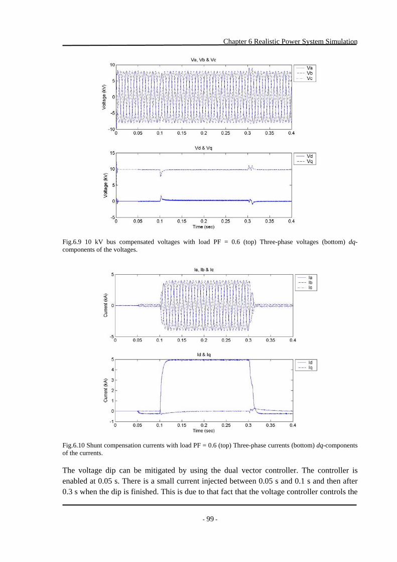
Chapter 6 Realistic Power System Simulation
99
Fig.6.9 10 kV bus compensated voltages with load PF = 0.6 (top) Three-phase voltages (bottom) dq- components of the voltages.
Fig.6.10 Shunt compensation currents with load PF = 0.6 (top) Three-phase currents (bottom) dq-components of the currents. The voltage dip can be mitigated by using the dual vector controller. The controller is enabled at 0.05 s. There is a small current injected between 0.05 s and 0.1 s and then after 0.3 s when the dip is finished. This is due to that fact that the voltage controller controls the
- -
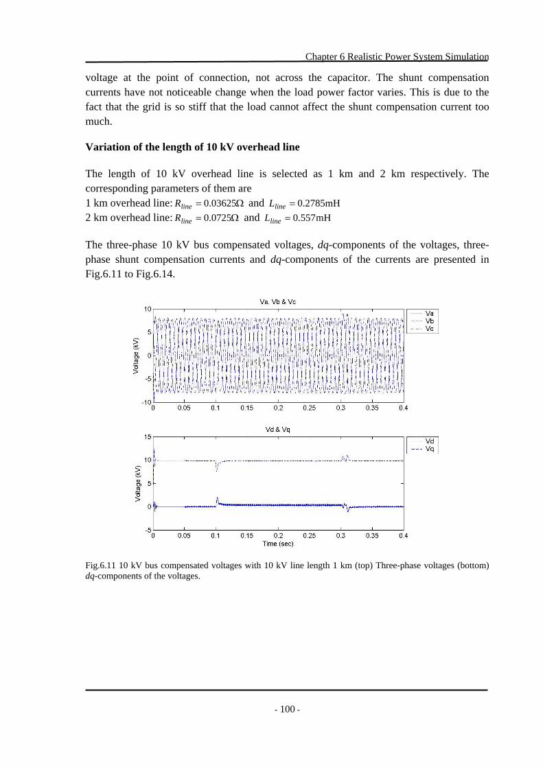
Chapter 6 Realistic Power System Simulation
100
voltage at the point of connection, not across the capacitor. The shunt compensation currents have not noticeable change when the load power factor varies. This is due to the fact that the grid is so stiff that the load cannot affect the shunt compensation current too much. Variation of the length of 10 kV overhead line The length of 10 kV overhead line is selected as 1 km and 2 km respectively. The corresponding parameters of them are 1 km overhead line: Ω= 03625.0lineR and mH2785.0=lineL 2 km overhead line: Ω= 0725.0lineR and mH557.0=lineL The three-phase 10 kV bus compensated voltages, dq-components of the voltages, three-phase shunt compensation currents and dq-components of the currents are presented in Fig.6.11 to Fig.6.14.
Fig.6.11 10 kV bus compensated voltages with 10 kV line length 1 km (top) Three-phase voltages (bottom) dq-components of the voltages.
- -
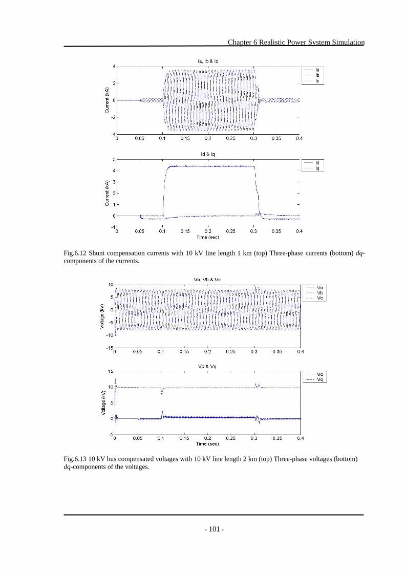
Chapter 6 Realistic Power System Simulation
101
Fig.6.12 Shunt compensation currents with 10 kV line length 1 km (top) Three-phase currents (bottom) dq- components of the currents.
Fig.6.13 10 kV bus compensated voltages with 10 kV line length 2 km (top) Three-phase voltages (bottom) dq-components of the voltages.
- -
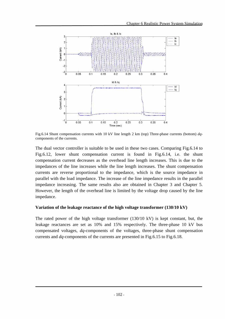
Chapter 6 Realistic Power System Simulation
102
Fig.6.14 Shunt compensation currents with 10 kV line length 2 km (top) Three-phase currents (bottom) dq- components of the currents. The dual vector controller is suitable to be used in these two cases. Comparing Fig.6.14 to Fig.6.12, lower shunt compensation current is found in Fig.6.14, i.e. the shunt compensation current decreases as the overhead line length increases. This is due to the impedances of the line increases while the line length increases. The shunt compensation currents are reverse proportional to the impedance, which is the source impedance in parallel with the load impedance. The increase of the line impedance results in the parallel impedance increasing. The same results also are obtained in Chapter 3 and Chapter 5. However, the length of the overhead line is limited by the voltage drop caused by the line impedance. Variation of the leakage reactance of the high voltage transformer (130/10 kV) The rated power of the high voltage transformer (130/10 kV) is kept constant, but, the leakage reactances are set as 10% and 15% respectively. The three-phase 10 kV bus compensated voltages, dq-components of the voltages, three-phase shunt compensation currents and dq-components of the currents are presented in Fig.6.15 to Fig.6.18.
- -
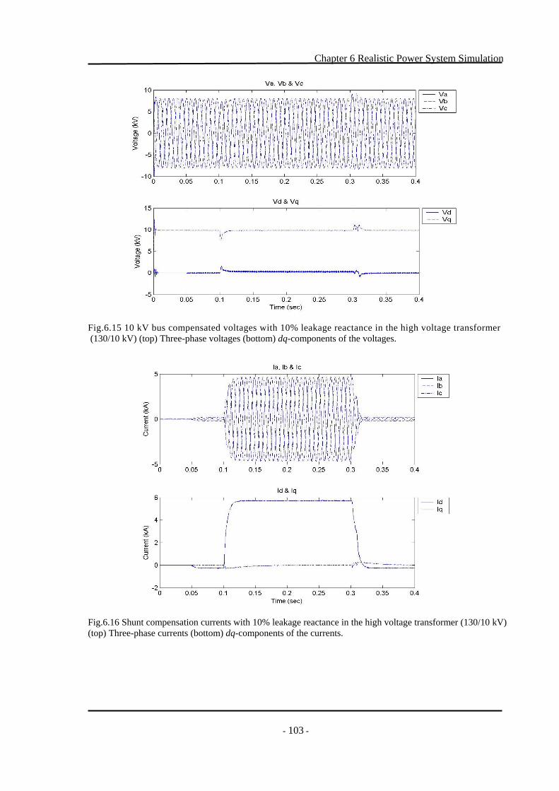
Chapter 6 Realistic Power System Simulation
103
Fig.6.15 10 kV bus compensated voltages with 10% leakage reactance in the high voltage transformer (130/10 kV) (top) Three-phase voltages (bottom) dq-components of the voltages.
Fig.6.16 Shunt compensation currents with 10% leakage reactance in the high voltage transformer (130/10 kV) (top) Three-phase currents (bottom) dq-components of the currents.
- -

Chapter 6 Realistic Power System Simulation
104
Fig.6.17 10 kV bus compensated voltages with 15% leakage reactance in the high voltage transformer (130/10 kV) (top) Three-phase voltages (bottom) dq-components of the voltages.
Fig.6.18 Shunt compensation currents with 15% leakage reactance in the high voltage transformer (130/10 kV) (top) Three-phase currents (bottom) dq-components of the currents.
- -
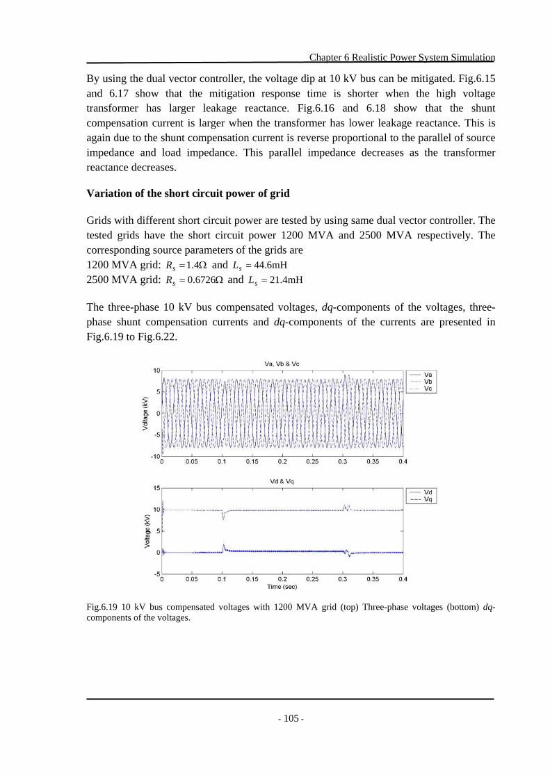
Chapter 6 Realistic Power System Simulation
105
By using the dual vector controller, the voltage dip at 10 kV bus can be mitigated. Fig.6.15 and 6.17 show that the mitigation response time is shorter when the high voltage transformer has larger leakage reactance. Fig.6.16 and 6.18 show that the shunt compensation current is larger when the transformer has lower leakage reactance. This is again due to the shunt compensation current is reverse proportional to the parallel of source impedance and load impedance. This parallel impedance decreases as the transformer reactance decreases. Variation of the short circuit power of grid Grids with different short circuit power are tested by using same dual vector controller. The tested grids have the short circuit power 1200 MVA and 2500 MVA respectively. The corresponding source parameters of the grids are 1200 MVA grid: and Ω= 4.1sR mH6.44=sL 2500 MVA grid: and Ω= 6726.0sR mH4.21=sL The three-phase 10 kV bus compensated voltages, dq-components of the voltages, three-phase shunt compensation currents and dq-components of the currents are presented in Fig.6.19 to Fig.6.22.
Fig.6.19 10 kV bus compensated voltages with 1200 MVA grid (top) Three-phase voltages (bottom) dq- components of the voltages.
- -
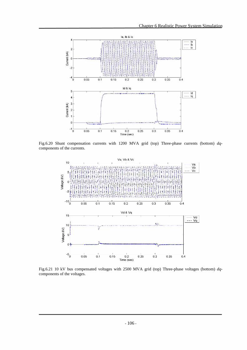
Chapter 6 Realistic Power System Simulation
106
Fig.6.20 Shunt compensation currents with 1200 MVA grid (top) Three-phase currents (bottom) dq- components of the currents.
Fig.6.21 10 kV bus compensated voltages with 2500 MVA grid (top) Three-phase voltages (bottom) dq- components of the voltages.
- -
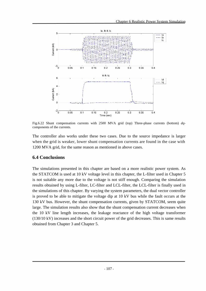
Chapter 6 Realistic Power System Simulation
107
Fig.6.22 Shunt compensation currents with 2500 MVA grid (top) Three-phase currents (bottom) dq- components of the currents. The controller also works under these two cases. Due to the source impedance is larger when the grid is weaker, lower shunt compensation currents are found in the case with 1200 MVA grid, for the same reason as mentioned in above cases. 6.4 Conclusions The simulations presented in this chapter are based on a more realistic power system. As the STATCOM is used at 10 kV voltage level in this chapter, the L-filter used in Chapter 5 is not suitable any more due to the voltage is not stiff enough. Comparing the simulation results obtained by using L-filter, LC-filter and LCL-filter, the LCL-filter is finally used in the simulations of this chapter. By varying the system parameters, the dual vector controller is proved to be able to mitigate the voltage dip at 10 kV bus while the fault occurs at the 130 kV bus. However, the shunt compensation currents, given by STATCOM, seem quite large. The simulation results also show that the shunt compensation current decreases when the 10 kV line length increases, the leakage reactance of the high voltage transformer (130/10 kV) increases and the short circuit power of the grid decreases. This is same results obtained from Chapter 3 and Chapter 5.
- -
Chapter 7 Conclusions
108
Chapter 7
Conclusions The objective of this thesis is to study the performance of the STATCOM for mitigating voltage dips. The analysis was composed of two parts, one is theoretical analysis, and the other is designing a controller of the STATCOM for mitigating the voltage dips. Being a shunt device, the STATCOM is considered as a current source to contribute to the mitigation of the voltage dip. In order to analyze the contribution of the STATCOM to the load terminal voltage boost during the dip, three analysis models were built: the power system before the fault, the power system without the compensation during the dip and the power system with the compensation during the dip. Equations used to calculate the shunt compensation current for constant impedance load and constant current load were derived. To be able to verify these equations, a simplified single-phase simulation circuit was built in the PSCAD/EMTDC. The STATCOM is considered as a controllable current source. By using the shunt compensation current calculated by the derived equations as the control signal of the controllable current source, the load terminal voltage can be mitigated exactly to 1 pu. This proved that the equations are correct. Based on these equations, the characteristics of the STATCOM for mitigating voltage dips are studied by using a general data of power system and of a more realistic power system model. The results show:
- For the different load characteristics (constant impedance load and constant current load), the shunt compensation current, active and reactive power increase when the voltage dip magnitude decreases.
- The shunt compensation current, active and reactive power decrease when the load power factor increases for the same dip magnitude.
- The shunt compensation current, active and reactive power decrease as the source impedance increases for the same dip magnitude. This also means that the STATCOM will inject less current for dip mitigation in the weaker grid.
- The STATCOM will inject less shunt compensation current, active and reactive power into the power system if the device is installed closer to the sensitive load. Larger shunt compensation current is required if the fault is closer to the STATCOM. Thus, the STATCOM cannot be used to protect from faults at the same bus.
All these results present that the shunt compensation current is reverse proportional to the impedance, which is the source impedance in parallel with the load impedance.
- -
Chapter 7 Conclusions
109
The dual vector controller, which is composed of vector current controller (inner control loop) and vector voltage controller (outer control loop), was designed for mitigating the voltage dip by STATCOM. In order to obtain high dynamic performance of the controller, deadbeat gain is used in the vector current controller. The step response simulation of the vector current controller is done in the Matlab/Simulink. The results show that there is only one cycle delay between the reference and the real active or reactive currents when step is given to one current. Due to the controller implemented in the computer, it brings the transformation angle error and the calculation time delay. Therefore, the transformation angle compensation and the delay time compensation are added into the state space equations of the controller. The simulation results show that the step responses of the active and reactive current, and cross coupling between the two currents, are much better when the compensation is used. The step response of the vector voltage controller and the dual vector controller are also tested in this thesis by using EMTDC and Simulink respectively. The results show that the real variables can track the reference values. To test the dynamic performance of the controller of the STATCOM for mitigating the voltage dip, three simulation models were built in PSCAD/EMTDC. First one is the simplified three-phase system model with three controllable current sources to represent the STATCOM. The control signal of the current source is the output of the vector voltage controller. The simulation results show that the voltage dip at the load terminal can be mitigated. The shortcoming of this model is that the mitigation response time is long. The second model is the simplified three-phase system with three controllable voltage sources to represent the Voltage Source Converter (VSC). The control signal of the voltage source is the output of the vector current controller. By using the reactive power control in the vector voltage controller and dead-beat gain in the vector current controller, perfect simulation result is obtained. The voltage dip at the load terminal can be mitigated in 5 ms. The shortcoming of this controller is that only reactive power injected into the power system, therefore a phase angle jump will occur in the voltage during the dip. The third model is the three-phase system with real converter model. This model is more realistic. A 400 V low voltage simulation circuit and a realistic power system, in which the STATCOM is installed at 10 kV bus, are tested respectively. When applying the STATCOM in a 10 kV system, the STATCOM configuration must be changed by replacing the L-filter with LCL-filter. In order to verify that the controller is robust or not, the various system parameters are tested by using the same controller parameters. Results show that the STATCOM with LCL-filter has robust performance, but the reactive current requirements are very high. The simulation results obtain the same characteristics of the shunt compensation current again, which is reverse proportional to the parallel impedance (source impedance in parallel with the load impedance).
- -
References
- 110 -
References [1] Beaulieu G., Bollen, M.H.J, Malgarotti S. and Ball R., Power quality indices and
objectives. Ongoing activities in CIGRE WG 36-07. Power Engineering Society Summer Meeting, 2002. IEEE, Volume: 2, 21-25 July 2002, Pages: 789 – 794 vol.2
[2] M.H.J. Bollen, Understanding Power Quality Problems: Voltage Sags and
Interruptions. New York, IEEE Press, 1999. [3] Ambra Sannino, Power Quality and Electromagnetic Compatibility Courses
Compendium, Chalmers University of Technology, Dept. of Electric Power Engineering, Spring 2004.
[4] M.H.J. Bollen, L.D.Zhang, Different methods for classification of three-phase
unbalanced voltage dips due to faults. Electric Power Systems Research, Volume 66, Issue 1 2003, pages 59-69
[5] Ambra Sannino, Michelle Ghans Miller, Math H.J. Bollen, Overview of Voltage Sag
Mitigation. Power Engineering Society Winter Meeting, 2000. IEEE, Volume: 4, 23-27 Jan, 2000, pages: 2872 – 2878 vol.4
[6] A. Sannino, J. Svensson, T. Larsson, Power-electronic solutions to power-quality
problems, Electric Power Systems Research, Volume 66, Issue 1, July 2003, pages 71 – 82
[7] M.F. McGranaghan, D.R.Mueller, M.J.Samotyj, Voltage sags in industrial systems,
IEEE Trans. Industry Applications, Vol.29, no.2, March/April 1993, pp.397 – 403 [8] Narain G. Hingorani and Laszlo Gyugyi, Understanding FACTS Concepts and
Technology of Flexible AC Transmission Systems. New York, IEEE Press, 2000. [9] K. Linden, I. Segerqvist, Modeling of Load Devices and Studying Load/System
Characteristics, Department of Electric Power Engineering, Tech. Rep., 1992 [10] Jan Svensson, Grid-connected Voltage Source Converter- Control Principles and
Wind Energy Applications, Ph.D. thesis, Chalmers University of Technology, Technical Report no.331, March 1998
[11] Wang P., Jenkins N. and Bollen M.H.J, Experimental Investigation of Voltage Sag
Mitigation by An Advanced Static Var Compensator, Power Delivery, IEEE Transactions on, Volume: 13, Issue: 4, Oct. 1998. Pages: 1461 – 1467
[12] D.R. Trainer, S.B. Tennakoon and R.E. Morrison, Analysis of GTO-based Static
Var Compensators, IEEE Proceedings – Electric Power Application, Vol.141, No.6, Nov 1994
References
- 111 -
[13] G. Saccomando, Grid-connected VSC Operating Under Voltage Disturbance Conditions, Masters thesis, Department of Electric Power Engineering, Chalmers University of Technology, Report No. 18R, 2000
[14] Jan Svensson, Voltage Source Converter control and PWM modulation, Power
Electronics 2 Compedium, Department of Electric Power Engineering, Chalmers University of Technology, Jan 2004
[15] V. Kaura and V. Blasko, Operation of a Voltage Source Converter at Increased
Utility Voltage, IEEE Transactions on Power Electronics, Vol.12, No. 1, Jan 1997, pp. 132 – 137
[16] Jonas Ottosson and Marcus Rudberg, Simplified models for two- and three-level
Voltage Source Converters, Masters Thesis, Department of Electric Power Engineering, Chalmers University of Technology. March 2003.
[17] Lindgren M. and Svensson J, Control of a voltage-source converter connected to
the grid through an LCL-filter-application to active filtering, Power Electronics Specialists Conference, 1998. PESC 98 Record. 29th Annual. IEEE, Volume: 1, 17 – 22 May 1998. Pages: 229 – 235 vol.1
[18] Guan-Chyun Hsieh and Hung J.C, Phase-locked loop techniques, A survey,
Industrial Electronics, IEEE Transactions on, Volume: 43, Issue: 6, Dec. 1996. Pages: 609 – 615
[19] Bollen M.H.J, Transmission & Distribution Compendium, Department of Electric
Power Engineering, Chalmers University of Technology.
Appendix A Transformations for Three-phase Systems
Appendix A
Transformations for Three-phase Systems The transformations described in this Appendix are called ‘Clarke Transformation’ and ‘Park Transformation’. This is an important tool used in the controller. By using this transformation, the voltage and current instantaneous value can be transformed between three-phase system and αβ-frame, and, between αβ-frame and dq-frame. Then dc quantities, which are easier to be control, can be obtained. A.1 Transformation between Three-phase systems and αβ-frame The three-phase instantaneous quantities , and in positive system can be transformed into a vector
)(1 tx )(2 tx )(3 tx)(j)( txtx βα + in the fixed two-axis coordinate system, called αβ-
frame. The vector in αβ-frame is defined by
⎟⎟
⎠
⎞
⎜⎜
⎝
⎛⋅+⋅+=+=
ππ
βα34j
332j
21 e)(e)()()(j)( txtxtxKtxtxx (A.1)
Where K is the factor to keep the power invariance between the two systems. It is usually
equal to 32 . By adding the zero component , the transformation is described as )(0 tx
⎥⎥⎥
⎦
⎤
⎢⎢⎢
⎣
⎡
⎥⎥⎥⎥⎥⎥
⎦
⎤
⎢⎢⎢⎢⎢⎢
⎣
⎡
−
−−
=⎥⎥⎥
⎦
⎤
⎢⎢⎢
⎣
⎡
)()()(
21
21
21
23
230
21
211
32
)()()(
3
2
1
0 txtxtx
txtxtx
β
α
(A.2)
And the inverse can be written as
⎥⎥⎥
⎦
⎤
⎢⎢⎢
⎣
⎡
⎥⎥⎥⎥⎥⎥⎥
⎦
⎤
⎢⎢⎢⎢⎢⎢⎢
⎣
⎡
−−
−=⎥⎥⎥
⎦
⎤
⎢⎢⎢
⎣
⎡
)()()(
21
23
21
21
23
21
2101
32
)()()(
03
2
1
txtxtx
txtxtx
β
α
(A.3)
If the system is symmetric, the sum of the three phase quantities is zero and the zero component is zero. Then the Eq.(A.2) becomes )(0 tx
- 112 -
Appendix A Transformations for Three-phase Systems
⎥⎥⎥
⎦
⎤
⎢⎢⎢
⎣
⎡
⎥⎥⎥⎥
⎦
⎤
⎢⎢⎢⎢
⎣
⎡
−=⎥
⎦
⎤⎢⎣
⎡
)()()(
21
210
0023
)()(
3
2
1
txtxtx
txtx
β
α (A.4)
And the inverse is
⎥⎦
⎤⎢⎣
⎡
⎥⎥⎥⎥⎥⎥⎥
⎦
⎤
⎢⎢⎢⎢⎢⎢⎢
⎣
⎡
−−
−=⎥⎥⎥
⎦
⎤
⎢⎢⎢
⎣
⎡
)()(
21
61
21
61
032
)()()(
3
2
1
txtx
txtxtx
β
α (A.5)
A.2 The transformation between αβ-frame and the dq-frame Let the vectors )(v t and )(w t rotate in the αβ-frame with the angular frequency ω(t) in the positive (counter-clockwise) direction. If the vector )(w t is taken as the d-axis of a dq-frame that rotates in the same direction with the angular frequency ω(t), both vector )(v t and )(w t will appear as fixed vectors in that frame. The components of )(v t in the dq-frame are therefore given by the projections of the vector on the direction of )(w t and the orthogonal direction, as displayed in Fig.A.1.
)(tθ
α
β
)(v t
)(v tα
)(v tβ)(tω)(tθ∆
)(tω
d
q
)(w t
Fig.A.1 Relation between αβ-frame and dq-frame
The transformation can be written in vector form as
)(v)(v )()(j)( tet αβtdq θ−= (A.6) Where the angle θ(t) is given by
(0))( θdτω(τ)tθ t0 += ∫ (A.7)
- 113 -
Appendix A Transformations for Three-phase Systems And the inverse transformation from dq-frame to αβ-frame is given by
)(v)(v )()(j)( tet dqtαβ θ= (A.8) The component in the dq-frame can be determined from the Fig.A.1. The transformation from αβ-frame to dq-frame in matrix form can be written as
⎥⎦
⎤⎢⎣
⎡−=⎥
⎦
⎤⎢⎣
⎡
β
α
)()(
))(()()(
tvtv
tθRtvtv
q
d (A.9)
And the inverse is
⎥⎦
⎤⎢⎣
⎡=⎥
⎦
⎤⎢⎣
⎡
β
α
)()(
))(()()(
tvtv
tθRtvtv
q
d (A.10)
Where the projection matrix R(θ(t)) is given by
⎥⎦
⎤⎢⎣
⎡ −=θ
))(cos())(sin())(sin())(cos(
))((tθtθtθtθ
tR (A.11)
A.2.1 Grid-flux oriented transformations of voltages and currents A three-phase sinusoidal voltage can be transformed into a vector )(je)()( ttete βα += in αβ-frame by assuming it is symmetrical and with angular frequency ω(t). When it is further transformed into dq-frame, the d-axis of the dq-frame is defined as parallel and synchronized to the grid flux vector )(tψ . In steady state, the flux vector is phase-shifted 90º after the voltage vector )(te . Consequently, the voltage vector )(te will only contain the q component in the dq-frame under this definition of the reference vector. The transformation equation for a current vector from the αβ-frame to dq-frame is given by
⎥⎦
⎤⎢⎣
⎡π−−=⎥
⎦
⎤⎢⎣
⎡)()(
))2
((R)()(
titi
ωttiti
β
α
q
d (A.12)
And the inverse is
⎥⎦
⎤⎢⎣
⎡π−=⎥
⎦
⎤⎢⎣
⎡ α
)()(
)2
(R)()(
titi
ωttiti
q
d
β (A.13)
The voltage vector transformations between αβ-frame and dq-frame are same with those for current vectors.
- 114 -
Appendix B Phase-Locked Loop (PLL)
Appendix B
Phase-Locked Loop (PLL) Phase-Locked loop (PLL) is a technique that is used to obtain an accurate synchronisation to the grid. It is implemented in almost all electronic equipments connected to the grid. The analogue PLL and software PLL are presented in [10] [18]. As shown in Fig.A.1, there is a transformation angle θ(t) between αβ-frame and dq-frame. This transformation angle can be obtained by using PLL and thus ensure the dq-frame is synchronised to the grid, so called synchronous reference frame (SRF). If the voltage vector
βα += eee j is defined as parallel with the q-axis in the dq-frame, the transformation angle θ(t) in Fig.A.1 can be defined as
ee
θ β=sin (B.1)
And
ee
θ α−=cos (B.2)
This can be implemented in the EMTDC, as shown in Fig.B.1. The three-phase instantaneous voltages are denoted by , and . The corresponding voltages transformed into αβ-frame are denoted by and . This block is used in this thesis.
ae be ceαe βe
abc / αβ
x2
*
x2
*
x
N/D
N/D
N
D
ND
θsin
θcos
αe
βe
)(αβe
ae
be
ce
Fig.B.1 PLL block implemented in EMTDC.
- 115 -
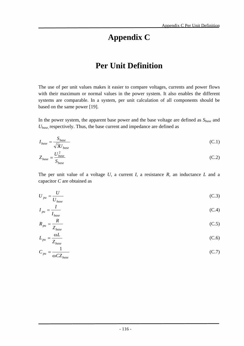
Appendix C Per Unit Definition
Appendix C
Per Unit Definition The use of per unit values makes it easier to compare voltages, currents and power flows with their maximum or normal values in the power system. It also enables the different systems are comparable. In a system, per unit calculation of all components should be based on the same power [19]. In the power system, the apparent base power and the base voltage are defined as Sbase and Ubase, respectively. Thus, the base current and impedance are defined as
base
basebase U
SI
3= (C.1)
base
basebase S
UZ
2
= (C.2)
The per unit value of a voltage U, a current I, a resistance R, an inductance L and a capacitor C are obtained as
basepu U
UU = (C.3)
basepu I
II = (C.4)
basepu Z
RR = (C.5)
basepu Z
LL ω= (C.6)
basepu CZ
Cω
=1 (C.7)
- 116 -