analysis and mitigation of seu-induced noise in fpga-based
TRANSCRIPT

Brigham Young University Brigham Young University
BYU ScholarsArchive BYU ScholarsArchive
Theses and Dissertations
2011-02-11
Analysis and Mitigation of SEU-induced Noise in FPGA-based DSP Analysis and Mitigation of SEU-induced Noise in FPGA-based DSP
Systems Systems
Brian Hogan Pratt Brigham Young University - Provo
Follow this and additional works at: https://scholarsarchive.byu.edu/etd
Part of the Electrical and Computer Engineering Commons
BYU ScholarsArchive Citation BYU ScholarsArchive Citation Pratt, Brian Hogan, "Analysis and Mitigation of SEU-induced Noise in FPGA-based DSP Systems" (2011). Theses and Dissertations. 2482. https://scholarsarchive.byu.edu/etd/2482
This Dissertation is brought to you for free and open access by BYU ScholarsArchive. It has been accepted for inclusion in Theses and Dissertations by an authorized administrator of BYU ScholarsArchive. For more information, please contact [email protected], [email protected].
Analysis and Mitigation of SEU-induced Noise
in FPGA-based DSP Systems
Brian H. Pratt
A dissertation submitted to the faculty ofBrigham Young University
in partial fulfillment of the requirements for the degree of
Doctor of Philosophy
Michael J. Wirthlin, ChairBrent E. NelsonMichael D. RiceDavid A. PenryDoran K. Wilde
Department of Electrical and Computer Engineering
Brigham Young University
April 2011
Copyright c© 2011 Brian H. Pratt
All Rights Reserved


ABSTRACT
Analysis and Mitigation of SEU-induced Noise
in FPGA-based DSP Systems
Brian H. Pratt
Department of Electrical and Computer Engineering
Doctor of Philosophy
This dissertation studies the effects of radiation-induced single-event upsets (SEUs)on digital signal processing (DSP) systems designed for field-programmable gate arrays (FP-GAs). It presents a novel method for evaluating the effects of radiation on DSP and digitalcommunication systems. By using an application-specific measurement of performance inthe presence of SEUs, this dissertation demonstrates that only 5–15% of SEUs affecting acommunications receiver (i.e. 5–15% of sensitive SEUs) cause critical performance loss. Italso reports that the most critical SEUs are those that affect the clock, global reset, andmost significant bits (MSBs) of computation.
This dissertation also demonstrates reduced-precision redundancy (RPR) as an effec-tive and efficient alternative to the popular triple modular redundancy (TMR) for FPGA-based communications systems. Fault injection experiments show that RPR can improvethe failure rate of a communications system by over 20 times over the unmitigated systemat a cost less than half that of TMR by focusing on the critical SEUs. This dissertationcontrasts the cost and performance of three different variations of RPR, one of which is anovel variation developed here, and concludes that the variation referred to as “ThresholdRPR” is superior to the others for FPGA systems. Finally, this dissertation presents severalmethods for applying Threshold RPR to a system with the goal of reducing mitigation costand increasing the system performance in the presence of SEUs. Additional fault injectionexperiments show that optimizing the application of RPR can result in a decrease in criticalSEUs by as much 65% at no additional hardware cost.
Keywords: FPGA, reliability, single-event upset, radiation effects, triple modular redun-dancy, reduced-precision redundancy, digital signal processing, digital communications


ACKNOWLEDGMENTS
This dissertation is the result of several years of hard work and wouldn’t have been
possible without the support of many people, to whom I am very grateful.
First and foremost, I would like to thank my family. My wife Aubrey has been my
inspiration and my best friend throughout the years of my studies. I thank her and our
daughter Celeste for their support, encouragement, and patience. I am also grateful to my
parents for the great start in life and for all the advice and support they have given me over
the years.
My professors at BYU assisted me in this work in many ways. I would like to thank
my advisor, Dr. Michael Wirthlin, for his guidance during this process. He helped me find a
path of research that I am excited to share and encouraged me when things didn’t go quite
as planned. Drs. Brent Nelson and Michael Rice were also great sources of assistance as I
planned what to do and how to do it.
I could not have made the contributions I have without the support and past re-
search of many BYU students. In particular, I’d like to thank Nathan Rollins, Jonathan
Johnson, Megan Fuller, Jon-Paul Anderson, Chris Lavin, Marc Padilla, William Howes,
Derrick Gibelyou, Keith Morgan, Daniel McMurtrey, and Eric Johnson.
I also would like to acknowledge the major sources of funding for the research that
went into this dissertation. The ISR division at Los Alamos National Laboratory has been a
longtime supporter of this and other work in FPGA reliability done at BYU. This research
was also supported by the I/UCRC Program of the National Science Foundation under Grant
No. 0801876 through the NSF Center for High-Performance Reconfigurable Computing
(CHREC).


TABLE OF CONTENTS
LIST OF TABLES . . . . . . . . . . . . . . . . . . . . . . . . . . . . . . . . . . . . xi
LIST OF FIGURES . . . . . . . . . . . . . . . . . . . . . . . . . . . . . . . . . . . xv
Chapter 1 Introduction . . . . . . . . . . . . . . . . . . . . . . . . . . . . . . . . 1
1.1 Motivation . . . . . . . . . . . . . . . . . . . . . . . . . . . . . . . . . . . . . 1
1.2 Summary of Research . . . . . . . . . . . . . . . . . . . . . . . . . . . . . . . 3
1.3 Dissertation Organization . . . . . . . . . . . . . . . . . . . . . . . . . . . . 4
Chapter 2 Radiation Effects and Mitigation on FPGAs . . . . . . . . . . . . 7
2.1 Single Event Effects . . . . . . . . . . . . . . . . . . . . . . . . . . . . . . . . 7
2.1.1 Types of Single Event Effects . . . . . . . . . . . . . . . . . . . . . . 8
2.1.2 SEE within ASICs . . . . . . . . . . . . . . . . . . . . . . . . . . . . 8
2.1.3 SEE within FPGAs . . . . . . . . . . . . . . . . . . . . . . . . . . . . 9
2.1.4 SEUs on SRAM-based FPGAs . . . . . . . . . . . . . . . . . . . . . . 10
2.2 SEU Mitigation for FPGAs . . . . . . . . . . . . . . . . . . . . . . . . . . . 12
2.2.1 Configuration Scrubbing . . . . . . . . . . . . . . . . . . . . . . . . . 13
2.2.2 Redundancy Techniques . . . . . . . . . . . . . . . . . . . . . . . . . 14
2.2.3 Triple Modular Redundancy . . . . . . . . . . . . . . . . . . . . . . . 15
2.2.4 Application Specific Fault Tolerance . . . . . . . . . . . . . . . . . . 17
2.3 Evaluating FPGA Design Reliability . . . . . . . . . . . . . . . . . . . . . . 18
2.3.1 Sensitivity . . . . . . . . . . . . . . . . . . . . . . . . . . . . . . . . . 18
2.3.2 Fault Injection Experiments . . . . . . . . . . . . . . . . . . . . . . . 19
v
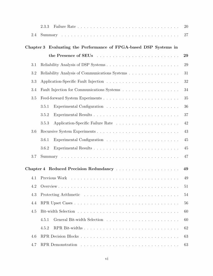
2.3.3 Failure Rate . . . . . . . . . . . . . . . . . . . . . . . . . . . . . . . . 20
2.4 Summary . . . . . . . . . . . . . . . . . . . . . . . . . . . . . . . . . . . . . 27
Chapter 3 Evaluating the Performance of FPGA-based DSP Systems in
the Presence of SEUs . . . . . . . . . . . . . . . . . . . . . . . . . . 29
3.1 Reliability Analysis of DSP Systems . . . . . . . . . . . . . . . . . . . . . . . 29
3.2 Reliability Analysis of Communications Systems . . . . . . . . . . . . . . . . 31
3.3 Application-Specific Fault Injection . . . . . . . . . . . . . . . . . . . . . . . 32
3.4 Fault Injection for Communications Systems . . . . . . . . . . . . . . . . . . 34
3.5 Feed-forward System Experiments . . . . . . . . . . . . . . . . . . . . . . . . 35
3.5.1 Experimental Configuration . . . . . . . . . . . . . . . . . . . . . . . 36
3.5.2 Experimental Results . . . . . . . . . . . . . . . . . . . . . . . . . . . 37
3.5.3 Application-Specific Failure Rate . . . . . . . . . . . . . . . . . . . . 42
3.6 Recursive System Experiments . . . . . . . . . . . . . . . . . . . . . . . . . . 43
3.6.1 Experimental Configuration . . . . . . . . . . . . . . . . . . . . . . . 45
3.6.2 Experimental Results . . . . . . . . . . . . . . . . . . . . . . . . . . . 45
3.7 Summary . . . . . . . . . . . . . . . . . . . . . . . . . . . . . . . . . . . . . 47
Chapter 4 Reduced Precision Redundancy . . . . . . . . . . . . . . . . . . . . 49
4.1 Previous Work . . . . . . . . . . . . . . . . . . . . . . . . . . . . . . . . . . 49
4.2 Overview . . . . . . . . . . . . . . . . . . . . . . . . . . . . . . . . . . . . . . 51
4.3 Protecting Arithmetic . . . . . . . . . . . . . . . . . . . . . . . . . . . . . . 54
4.4 RPR Upset Cases . . . . . . . . . . . . . . . . . . . . . . . . . . . . . . . . . 56
4.5 Bit-width Selection . . . . . . . . . . . . . . . . . . . . . . . . . . . . . . . . 60
4.5.1 General Bit-width Selection . . . . . . . . . . . . . . . . . . . . . . . 60
4.5.2 RPR Bit-widths . . . . . . . . . . . . . . . . . . . . . . . . . . . . . . 62
4.6 RPR Decision Blocks . . . . . . . . . . . . . . . . . . . . . . . . . . . . . . . 63
4.7 RPR Demonstration . . . . . . . . . . . . . . . . . . . . . . . . . . . . . . . 63
vi

4.7.1 Experimental Configuration . . . . . . . . . . . . . . . . . . . . . . . 64
4.7.2 Mitigation Details . . . . . . . . . . . . . . . . . . . . . . . . . . . . . 65
4.7.3 Experimental Results . . . . . . . . . . . . . . . . . . . . . . . . . . . 66
4.8 Summary . . . . . . . . . . . . . . . . . . . . . . . . . . . . . . . . . . . . . 71
Chapter 5 Comparison of RPR Variations . . . . . . . . . . . . . . . . . . . . 73
5.1 RPR Variations . . . . . . . . . . . . . . . . . . . . . . . . . . . . . . . . . . 73
5.1.1 Threshold RPR . . . . . . . . . . . . . . . . . . . . . . . . . . . . . . 74
5.1.2 Bounded RPR . . . . . . . . . . . . . . . . . . . . . . . . . . . . . . . 78
5.1.3 RP-TMR . . . . . . . . . . . . . . . . . . . . . . . . . . . . . . . . . 82
5.2 RPR Variation Comparison . . . . . . . . . . . . . . . . . . . . . . . . . . . 86
5.2.1 Decision Block Cost . . . . . . . . . . . . . . . . . . . . . . . . . . . 86
5.2.2 Reduced-precision Module Implementation . . . . . . . . . . . . . . . 87
5.2.3 Upset Cases . . . . . . . . . . . . . . . . . . . . . . . . . . . . . . . . 88
5.2.4 Error Detection Limits . . . . . . . . . . . . . . . . . . . . . . . . . . 91
5.2.5 Suitability for FPGAs . . . . . . . . . . . . . . . . . . . . . . . . . . 93
5.2.6 Summary . . . . . . . . . . . . . . . . . . . . . . . . . . . . . . . . . 94
5.3 Fault Injection Experiments . . . . . . . . . . . . . . . . . . . . . . . . . . . 95
5.3.1 Experimental Configuration . . . . . . . . . . . . . . . . . . . . . . . 95
5.3.2 Experimental Results . . . . . . . . . . . . . . . . . . . . . . . . . . . 96
5.4 Summary . . . . . . . . . . . . . . . . . . . . . . . . . . . . . . . . . . . . . 100
Chapter 6 Application of Threshold RPR . . . . . . . . . . . . . . . . . . . . . 103
6.1 Threshold Selection . . . . . . . . . . . . . . . . . . . . . . . . . . . . . . . . 104
6.1.1 Average Threshold RPR Noise Limit . . . . . . . . . . . . . . . . . . 104
6.1.2 Reduction of Th . . . . . . . . . . . . . . . . . . . . . . . . . . . . . . 105
6.1.3 Experimental Determination of Th . . . . . . . . . . . . . . . . . . . . 109
6.1.4 Reduced Threshold Experiments . . . . . . . . . . . . . . . . . . . . 112
vii
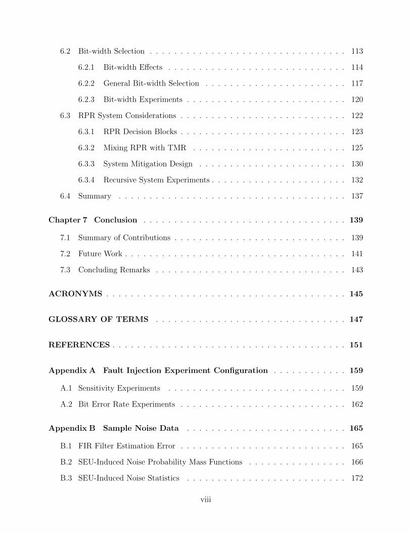
6.2 Bit-width Selection . . . . . . . . . . . . . . . . . . . . . . . . . . . . . . . . 113
6.2.1 Bit-width Effects . . . . . . . . . . . . . . . . . . . . . . . . . . . . . 114
6.2.2 General Bit-width Selection . . . . . . . . . . . . . . . . . . . . . . . 117
6.2.3 Bit-width Experiments . . . . . . . . . . . . . . . . . . . . . . . . . . 120
6.3 RPR System Considerations . . . . . . . . . . . . . . . . . . . . . . . . . . . 122
6.3.1 RPR Decision Blocks . . . . . . . . . . . . . . . . . . . . . . . . . . . 123
6.3.2 Mixing RPR with TMR . . . . . . . . . . . . . . . . . . . . . . . . . 125
6.3.3 System Mitigation Design . . . . . . . . . . . . . . . . . . . . . . . . 130
6.3.4 Recursive System Experiments . . . . . . . . . . . . . . . . . . . . . . 132
6.4 Summary . . . . . . . . . . . . . . . . . . . . . . . . . . . . . . . . . . . . . 137
Chapter 7 Conclusion . . . . . . . . . . . . . . . . . . . . . . . . . . . . . . . . . 139
7.1 Summary of Contributions . . . . . . . . . . . . . . . . . . . . . . . . . . . . 139
7.2 Future Work . . . . . . . . . . . . . . . . . . . . . . . . . . . . . . . . . . . . 141
7.3 Concluding Remarks . . . . . . . . . . . . . . . . . . . . . . . . . . . . . . . 143
ACRONYMS . . . . . . . . . . . . . . . . . . . . . . . . . . . . . . . . . . . . . . . 145
GLOSSARY OF TERMS . . . . . . . . . . . . . . . . . . . . . . . . . . . . . . . 147
REFERENCES . . . . . . . . . . . . . . . . . . . . . . . . . . . . . . . . . . . . . . 151
Appendix A Fault Injection Experiment Configuration . . . . . . . . . . . . 159
A.1 Sensitivity Experiments . . . . . . . . . . . . . . . . . . . . . . . . . . . . . 159
A.2 Bit Error Rate Experiments . . . . . . . . . . . . . . . . . . . . . . . . . . . 162
Appendix B Sample Noise Data . . . . . . . . . . . . . . . . . . . . . . . . . . 165
B.1 FIR Filter Estimation Error . . . . . . . . . . . . . . . . . . . . . . . . . . . 165
B.2 SEU-Induced Noise Probability Mass Functions . . . . . . . . . . . . . . . . 166
B.3 SEU-Induced Noise Statistics . . . . . . . . . . . . . . . . . . . . . . . . . . 172
viii
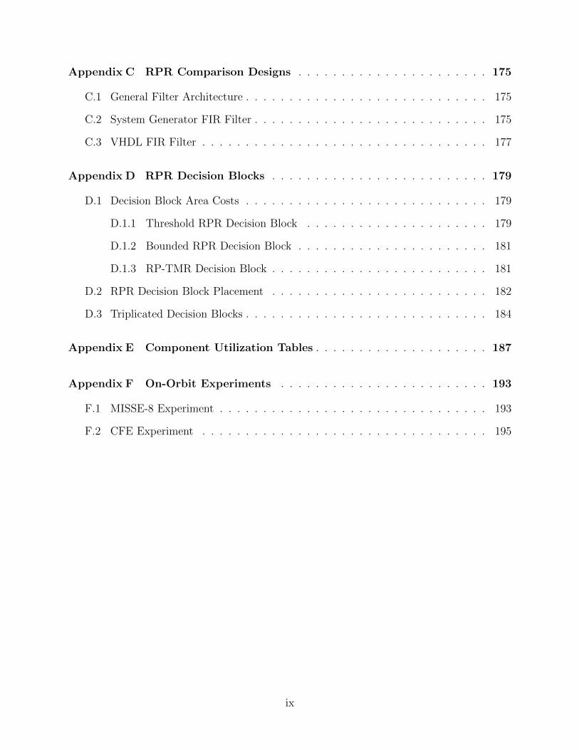
Appendix C RPR Comparison Designs . . . . . . . . . . . . . . . . . . . . . . 175
C.1 General Filter Architecture . . . . . . . . . . . . . . . . . . . . . . . . . . . . 175
C.2 System Generator FIR Filter . . . . . . . . . . . . . . . . . . . . . . . . . . . 175
C.3 VHDL FIR Filter . . . . . . . . . . . . . . . . . . . . . . . . . . . . . . . . . 177
Appendix D RPR Decision Blocks . . . . . . . . . . . . . . . . . . . . . . . . . 179
D.1 Decision Block Area Costs . . . . . . . . . . . . . . . . . . . . . . . . . . . . 179
D.1.1 Threshold RPR Decision Block . . . . . . . . . . . . . . . . . . . . . 179
D.1.2 Bounded RPR Decision Block . . . . . . . . . . . . . . . . . . . . . . 181
D.1.3 RP-TMR Decision Block . . . . . . . . . . . . . . . . . . . . . . . . . 181
D.2 RPR Decision Block Placement . . . . . . . . . . . . . . . . . . . . . . . . . 182
D.3 Triplicated Decision Blocks . . . . . . . . . . . . . . . . . . . . . . . . . . . . 184
Appendix E Component Utilization Tables . . . . . . . . . . . . . . . . . . . . 187
Appendix F On-Orbit Experiments . . . . . . . . . . . . . . . . . . . . . . . . 193
F.1 MISSE-8 Experiment . . . . . . . . . . . . . . . . . . . . . . . . . . . . . . . 193
F.2 CFE Experiment . . . . . . . . . . . . . . . . . . . . . . . . . . . . . . . . . 195
ix

x
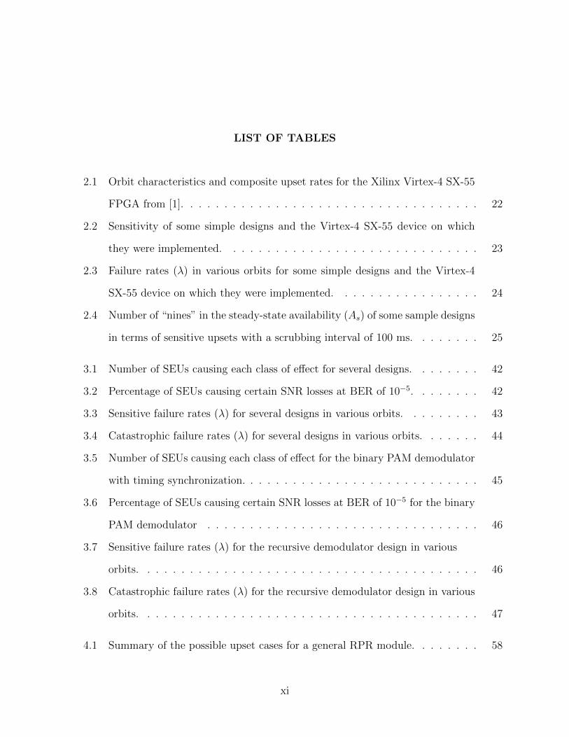
LIST OF TABLES
2.1 Orbit characteristics and composite upset rates for the Xilinx Virtex-4 SX-55
FPGA from [1]. . . . . . . . . . . . . . . . . . . . . . . . . . . . . . . . . . . 22
2.2 Sensitivity of some simple designs and the Virtex-4 SX-55 device on which
they were implemented. . . . . . . . . . . . . . . . . . . . . . . . . . . . . . 23
2.3 Failure rates (λ) in various orbits for some simple designs and the Virtex-4
SX-55 device on which they were implemented. . . . . . . . . . . . . . . . . 24
2.4 Number of “nines” in the steady-state availability (As) of some sample designs
in terms of sensitive upsets with a scrubbing interval of 100 ms. . . . . . . . 25
3.1 Number of SEUs causing each class of effect for several designs. . . . . . . . 42
3.2 Percentage of SEUs causing certain SNR losses at BER of 10−5. . . . . . . . 42
3.3 Sensitive failure rates (λ) for several designs in various orbits. . . . . . . . . 43
3.4 Catastrophic failure rates (λ) for several designs in various orbits. . . . . . . 44
3.5 Number of SEUs causing each class of effect for the binary PAM demodulator
with timing synchronization. . . . . . . . . . . . . . . . . . . . . . . . . . . . 45
3.6 Percentage of SEUs causing certain SNR losses at BER of 10−5 for the binary
PAM demodulator . . . . . . . . . . . . . . . . . . . . . . . . . . . . . . . . 46
3.7 Sensitive failure rates (λ) for the recursive demodulator design in various
orbits. . . . . . . . . . . . . . . . . . . . . . . . . . . . . . . . . . . . . . . . 46
3.8 Catastrophic failure rates (λ) for the recursive demodulator design in various
orbits. . . . . . . . . . . . . . . . . . . . . . . . . . . . . . . . . . . . . . . . 47
4.1 Summary of the possible upset cases for a general RPR module. . . . . . . . 58
xi
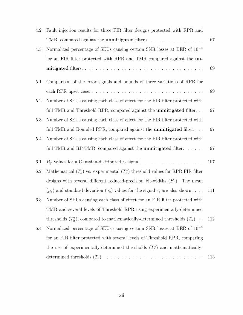
4.2 Fault injection results for three FIR filter designs protected with RPR and
TMR, compared against the unmitigated filters. . . . . . . . . . . . . . . . 67
4.3 Normalized percentage of SEUs causing certain SNR losses at BER of 10−5
for an FIR filter protected with RPR and TMR compared against the un-
mitigated filters. . . . . . . . . . . . . . . . . . . . . . . . . . . . . . . . . . 69
5.1 Comparison of the error signals and bounds of three variations of RPR for
each RPR upset case. . . . . . . . . . . . . . . . . . . . . . . . . . . . . . . . 89
5.2 Number of SEUs causing each class of effect for the FIR filter protected with
full TMR and Threshold RPR, compared against the unmitigated filter. . . 97
5.3 Number of SEUs causing each class of effect for the FIR filter protected with
full TMR and Bounded RPR, compared against the unmitigated filter. . . 97
5.4 Number of SEUs causing each class of effect for the FIR filter protected with
full TMR and RP-TMR, compared against the unmitigated filter. . . . . . 97
6.1 Pfp values for a Gaussian-distributed εe signal. . . . . . . . . . . . . . . . . . 107
6.2 Mathematical (Th) vs. experimental (T ∗h ) threshold values for RPR FIR filter
designs with several different reduced-precision bit-widths (Br). The mean
(µe) and standard deviation (σe) values for the signal εe are also shown. . . . 111
6.3 Number of SEUs causing each class of effect for an FIR filter protected with
TMR and several levels of Threshold RPR using experimentally-determined
thresholds (T ∗h ), compared to mathematically-determined thresholds (Th). . . 112
6.4 Normalized percentage of SEUs causing certain SNR losses at BER of 10−5
for an FIR filter protected with several levels of Threshold RPR, comparing
the use of experimentally-determined thresholds (T ∗h ) and mathematically-
determined thresholds (Th). . . . . . . . . . . . . . . . . . . . . . . . . . . . 113
xii

6.5 Detection factor (a) for an FIR filter protected with several levels of Threshold
RPR, comparing the use of experimentally-determined thresholds (T ∗h ) with
mathematically-determined thresholds (Th) at an SNR of 8 dB. . . . . . . . 113
6.6 Number of SEUs causing each class of effect for an FIR filter protected with
TMR and several levels of Threshold RPR using experimentally-determined
thresholds (T ∗h ), compared to the unmitigated filter. . . . . . . . . . . . . . 121
6.7 Estimated cost of several 4-tap FIR filter circuits protected with RPR. . . . 124
6.8 Number of SEUs causing each class of effect for the binary PAM demodulator
protected with full TMR and RPR+TMR, compared to the unmitigated
demodulator. . . . . . . . . . . . . . . . . . . . . . . . . . . . . . . . . . . . 136
6.9 Normalized percentage of SEUs causing certain SNR losses at BER of 10−5
for the binary PAM demodulator protected with full TMR and RPR+TMR. 137
A.1 Fault injection run times for each SNR input value. . . . . . . . . . . . . . . 164
C.1 Number of SEUs causing each class of effect for the FIR filter design with
α = 0.5. . . . . . . . . . . . . . . . . . . . . . . . . . . . . . . . . . . . . . . 176
C.2 Percentage of SEUs causing certain SNR losses at BER of 10−5 for the FIR
filter design with α = 0.5 . . . . . . . . . . . . . . . . . . . . . . . . . . . . . 177
C.3 Sensitive failure rates (λ) for the FIR filter design in various orbits. . . . . . 177
C.4 Catastrophic failure rates (λ) for the FIR filter design in various orbits. . . . 177
E.1 Resource utilization for two-input adder modules with a range of input bit-
widths. . . . . . . . . . . . . . . . . . . . . . . . . . . . . . . . . . . . . . . . 187
E.2 Resource utilization for single-input (constant coefficient) multiplier modules
with a range of input bit-widths. . . . . . . . . . . . . . . . . . . . . . . . . 188
E.3 Resource utilization for two-input multiplier modules with a range of input
bit-widths. . . . . . . . . . . . . . . . . . . . . . . . . . . . . . . . . . . . . . 189
E.4 Resource utilization for FIR filter modules with a range of input bit-widths. 189
xiii
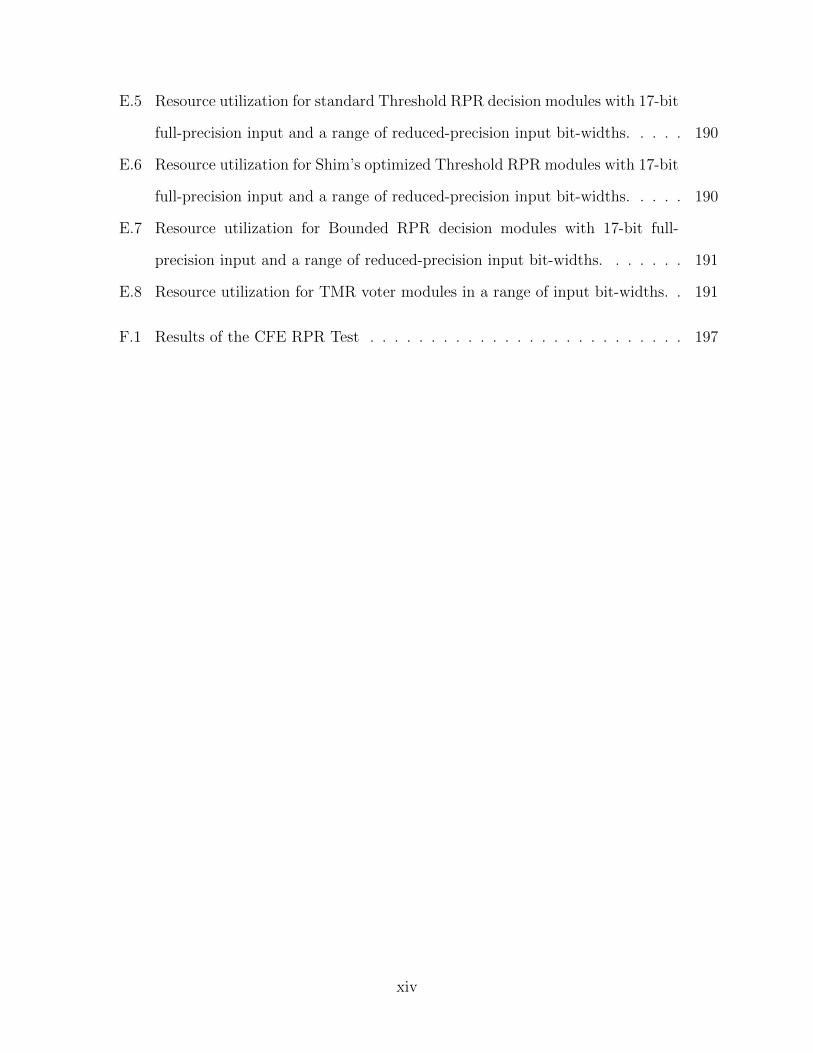
E.5 Resource utilization for standard Threshold RPR decision modules with 17-bit
full-precision input and a range of reduced-precision input bit-widths. . . . . 190
E.6 Resource utilization for Shim’s optimized Threshold RPR modules with 17-bit
full-precision input and a range of reduced-precision input bit-widths. . . . . 190
E.7 Resource utilization for Bounded RPR decision modules with 17-bit full-
precision input and a range of reduced-precision input bit-widths. . . . . . . 191
E.8 Resource utilization for TMR voter modules in a range of input bit-widths. . 191
F.1 Results of the CFE RPR Test . . . . . . . . . . . . . . . . . . . . . . . . . . 197
xiv
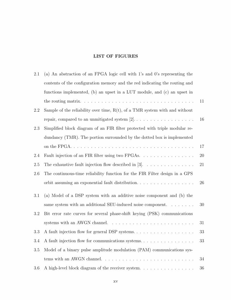
LIST OF FIGURES
2.1 (a) An abstraction of an FPGA logic cell with 1’s and 0’s representing the
contents of the configuration memory and the red indicating the routing and
functions implemented, (b) an upset in a LUT module, and (c) an upset in
the routing matrix. . . . . . . . . . . . . . . . . . . . . . . . . . . . . . . . . 11
2.2 Sample of the reliability over time, R(t), of a TMR system with and without
repair, compared to an unmitigated system [2]. . . . . . . . . . . . . . . . . . 16
2.3 Simplified block diagram of an FIR filter protected with triple modular re-
dundancy (TMR). The portion surrounded by the dotted box is implemented
on the FPGA. . . . . . . . . . . . . . . . . . . . . . . . . . . . . . . . . . . . 17
2.4 Fault injection of an FIR filter using two FPGAs. . . . . . . . . . . . . . . . 20
2.5 The exhaustive fault injection flow described in [3]. . . . . . . . . . . . . . . 21
2.6 The continuous-time reliability function for the FIR Filter design in a GPS
orbit assuming an exponential fault distribution. . . . . . . . . . . . . . . . . 26
3.1 (a) Model of a DSP system with an additive noise component and (b) the
same system with an additional SEU-induced noise component. . . . . . . . 30
3.2 Bit error rate curves for several phase-shift keying (PSK) communications
systems with an AWGN channel. . . . . . . . . . . . . . . . . . . . . . . . . 31
3.3 A fault injection flow for general DSP systems. . . . . . . . . . . . . . . . . . 33
3.4 A fault injection flow for communications systems. . . . . . . . . . . . . . . . 33
3.5 Model of a binary pulse amplitude modulation (PAM) communications sys-
tems with an AWGN channel. . . . . . . . . . . . . . . . . . . . . . . . . . . 34
3.6 A high-level block diagram of the receiver system. . . . . . . . . . . . . . . . 36
xv
3.7 The FIR filter structures examined in the fault injection experiments: (a)
direct form 1 FIR filter; (b) transposed direct form 1 FIR filter. . . . . . . . 37
3.8 BER plot showing representative samples from each of the four error classes
from the 16-bit logic-based FIR filter with α = 1.0. . . . . . . . . . . . . . . 38
3.9 BER plot for the 16-bit logic-based FIR filter with α = 1.0. . . . . . . . . . . 40
3.10 BER plot for the 16-bit logic-based FIR filter with α = 0.25. . . . . . . . . . 40
3.11 BER plot for the 8-bit logic-based FIR filter with α = 1.0. . . . . . . . . . . 40
3.12 BER plot for the 8-bit logic-based FIR filter with α = 0.25. . . . . . . . . . . 40
3.13 BER plot for the 16-bit DSP48-based FIR filter with α = 1.0. . . . . . . . . 41
3.14 BER plot for the 16-bit DSP48-based FIR filter with α = 0.25. . . . . . . . . 41
3.15 Block diagram of the binary PAM demodulator with timing synchronization. 44
3.16 BER plot for the unmitigated binary PAM receiver system with timing syn-
chronization. . . . . . . . . . . . . . . . . . . . . . . . . . . . . . . . . . . . . 46
4.1 Simplified block diagram of a module protected with reduced-precision redun-
dancy (RPR). . . . . . . . . . . . . . . . . . . . . . . . . . . . . . . . . . . . 51
4.2 Simplified block diagram of a module protected with reduced-precision redun-
dancy (RPR) designed for soft error environments. . . . . . . . . . . . . . . 53
4.3 Block diagram of an 8-bit register holding a fractional fixed-point number. . 55
4.4 Truncation of a fixed-point binary number to several levels of precision. . . . 61
4.5 Simplified block diagram of an 16-bit FIR filter protected with Threshold
RPR using two 8-bit filters as the reduced precision modules. . . . . . . . . . 65
4.6 BER plot for the 16-bit logic-based FIR filter with α = 1.0 with RPR using
two 8-bit reduced-precision filter replicas. . . . . . . . . . . . . . . . . . . . . 69
4.7 BER plot for the 16-bit logic-based FIR filter with α = 0.25 with RPR using
two 8-bit reduced-precision filter replicas. . . . . . . . . . . . . . . . . . . . . 69
4.8 BER plot for the 16-bit DSP Block-based FIR filter with α = 1.0 with RPR
using two 8-bit reduced-precision filter replicas. . . . . . . . . . . . . . . . . 70
xvi

5.1 Simplified block diagram of an n-bit (B = n) full-precision module protected
with Threshold RPR using two k-bit (Br = k) reduced-precision modules,
where k < n. . . . . . . . . . . . . . . . . . . . . . . . . . . . . . . . . . . . 75
5.2 Block diagram of a Threshold RPR decision block. . . . . . . . . . . . . . . 76
5.3 Block diagram of a optimization on the Threshold RPR decision block sug-
gested by Shim [4]. . . . . . . . . . . . . . . . . . . . . . . . . . . . . . . . . 77
5.4 Simplified block diagram of a full-precision module protected with Bounded
RPR using upper-bound and lower-bound reduced precision modules. . . . . 79
5.5 Error cases for Bounded RPR, modified from [5]. Categorized in rows by the
location of the error and in columns by the response to each type of event. . 79
5.6 Block diagram of a Bounded RPR decision block. Sign extensions, where
necessary, are not shown in this diagram. . . . . . . . . . . . . . . . . . . . . 81
5.7 Simplified block diagram of an n-bit full-precision module protected with
Bounded RPR using an add-and-subtract-threshold method of bounding the
full-precision output. . . . . . . . . . . . . . . . . . . . . . . . . . . . . . . . 82
5.8 Block diagram of an 8-bit register protected by RP-TMR. For simplicity, the
register inputs are not shown. The three clock domains are indicated by
dotted lines and are labeled clk1, clk2, and clk3. . . . . . . . . . . . . . . 83
5.9 Block diagram of an 8-bit adder protected by RP-TMR. For simplicity, the x
and y inputs of each full adder are not shown. The three clock domains, cor-
responding to the clock domains of the inputs to each full adder sub-module,
are indicated by dotted lines and are labeled clk1, clk2, and clk3. The full
adder submodule is detailed in the inset. . . . . . . . . . . . . . . . . . . . . 84
xvii

5.10 Block diagram of an array multiplier with annotations for RP-TMR. The
shading indicate the protected modules and the underlines note the replicated
partial product inputs. The full adder and half adder sub-modules used are
detailed in the insets, with each partial product shown as one input to each
module. . . . . . . . . . . . . . . . . . . . . . . . . . . . . . . . . . . . . . . 85
5.11 Relative cost of RPR decision blocks in terms of 4-input LUTs for a range of
reduced-precision bit-widths. . . . . . . . . . . . . . . . . . . . . . . . . . . . 87
5.12 Threshold RPR multiplier: full-precision output and reduced-precision output
with error bounds. h = 0.4921875, B = 7, Br = 3, and Th = εmax . . . . . . . 92
5.13 Bounded RPR multiplier: full-precision and reduced-precision outputs. h =
0.4921875, B = 7, and Br = 3. . . . . . . . . . . . . . . . . . . . . . . . . . . 93
5.14 Normalized percentage of SEUs causing certain SNR losses at BER of 10−5
for an FIR filter protected with three levels of Threshold RPR compared to
the unmitigated design. . . . . . . . . . . . . . . . . . . . . . . . . . . . . . . 100
5.15 Normalized percentage of SEUs causing certain SNR losses at BER of 10−5
for an FIR filter protected with three levels of Bounded RPR compared to the
unmitigated design. . . . . . . . . . . . . . . . . . . . . . . . . . . . . . . . . 101
5.16 Normalized percentage of SEUs causing certain SNR losses at BER of 10−5
for an FIR filter protected with three levels of RP-TMR compared to the
unmitigated design. . . . . . . . . . . . . . . . . . . . . . . . . . . . . . . . . 102
6.1 (a) The pmf of the estimation error, εe, of an RPR module, (b) the pmf for the
maximum undetected upset error signal, εu, and the pmf for (c) a mid-range
upset which crosses the reduced threshold, T ∗h . . . . . . . . . . . . . . . . . . 108
6.2 Bit error rate curves for several FIR filters (SRRC pulse shape, α = 0.5) with
different bit-widths. . . . . . . . . . . . . . . . . . . . . . . . . . . . . . . . . 115
xviii

6.3 RPR filter decision signals for RPR with Br = 6 and Th = 0.3106. No errors
are present in the system. The upper and lower comparison bound signals are
calculated by adding and subtracting Th to and from RPout. . . . . . . . . . 116
6.4 RPR filter decision signals for RPR with Br = 3 and Th = 2.3871. The FPout
signal is frozen at zero. The upper and lower comparison bound signals are
calculated by adding and subtracting Th to and from RPout. . . . . . . . . . 117
6.5 ERPR-avg of the FIR filter design for several bit-widths and using two failure
rates. . . . . . . . . . . . . . . . . . . . . . . . . . . . . . . . . . . . . . . . . 119
6.6 Normalized percentage of SEUs causing certain SNR losses at BER of 10−5
for an FIR filter protected with several levels of Threshold RPR compared to
the unmitigated design. . . . . . . . . . . . . . . . . . . . . . . . . . . . . . . 122
6.7 Block diagram of a 4-tap FIR filter. . . . . . . . . . . . . . . . . . . . . . . . 124
6.8 Workflow for choosing the location and number of decision blocks in an RPR
system. . . . . . . . . . . . . . . . . . . . . . . . . . . . . . . . . . . . . . . . 126
6.9 Block diagram of a simple circuit with feedback. . . . . . . . . . . . . . . . . 129
6.10 Workflow for applying RPR+TMR to a digital system. . . . . . . . . . . . . 131
6.11 Block diagram of the recursive binary PAM demodulator with annotations for
RPR+TMR. . . . . . . . . . . . . . . . . . . . . . . . . . . . . . . . . . . . . 133
6.12 Block diagram of the NCO block within the recursive binary PAM demodu-
lator, exported from Xilinx System Generator. . . . . . . . . . . . . . . . . . 134
6.13 BER plot for the binary PAM receiver system with timing synchronization
using RPR+TMR for mitigation. . . . . . . . . . . . . . . . . . . . . . . . . 137
A.1 A photograph of the fault injection test board. . . . . . . . . . . . . . . . . . 160
A.2 A block diagram of the ConfigMon FPGA used in the fault injection tests. . 160
A.3 Comparison between the (a) sensitivity test architecture and the (b) utiliza-
tion test architecture. . . . . . . . . . . . . . . . . . . . . . . . . . . . . . . . 162
A.4 A block diagram of the BER fault injection test. . . . . . . . . . . . . . . . . 164
xix

B.1 Probability mass function (pmf) of the estimation error, εe, of the reduced-
precision FIR Filter with Br = 2. . . . . . . . . . . . . . . . . . . . . . . . . 166
B.2 Probability mass function (pmf) of the estimation error, εe, the reduced-
precision FIR Filter with Br = 3. . . . . . . . . . . . . . . . . . . . . . . . . 166
B.3 Probability mass function (pmf) of the estimation error, εe, the reduced-
precision FIR Filter with Br = 4. . . . . . . . . . . . . . . . . . . . . . . . . 167
B.4 Probability mass function (pmf) of the estimation error, εe, the reduced-
precision FIR Filter with Br = 5. . . . . . . . . . . . . . . . . . . . . . . . . 167
B.5 Probability mass function (pmf) of the estimation error, εe, the reduced-
precision FIR Filter with Br = 6. . . . . . . . . . . . . . . . . . . . . . . . . 167
B.6 Probability mass function (pmf) of the estimation error, εe, the reduced-
precision FIR Filter with Br = 7. . . . . . . . . . . . . . . . . . . . . . . . . 167
B.7 Sample probability mass functions (pmfs) of the SEU-induced noise signals,
εu, for several upsets in an FIR filter design. . . . . . . . . . . . . . . . . . . 168
B.8 More sample probability mass functions (pmfs) of the SEU-induced noise sig-
nals, εu, for several upsets in an FIR filter design. . . . . . . . . . . . . . . . 169
B.9 More sample probability mass functions (pmfs) of the SEU-induced noise sig-
nals, εu, for several upsets in an FIR filter design. . . . . . . . . . . . . . . . 170
B.10 More sample probability mass functions (pmfs) of the SEU-induced noise sig-
nals, εu, for several upsets in an FIR filter design. . . . . . . . . . . . . . . . 171
B.11 Histogram of the mean of the SEU-induced noise signals, εu, for all sensitive
SEUs in an FIR filter design. . . . . . . . . . . . . . . . . . . . . . . . . . . . 173
B.12 Detail of the histogram in Figure B.11. . . . . . . . . . . . . . . . . . . . . . 173
B.13 Histogram of the variance of the SEU-induced noise signals, εu, for all sensitive
SEUs in an FIR filter design. . . . . . . . . . . . . . . . . . . . . . . . . . . . 173
B.14 Detail of the histogram in Figure B.13. . . . . . . . . . . . . . . . . . . . . . 173
xx
B.15 Histogram of the power (mean square) of the SEU-induced noise signals, εu,
for all sensitive SEUs in an FIR filter design. . . . . . . . . . . . . . . . . . . 174
B.16 Detail of the histogram in Figure B.15. . . . . . . . . . . . . . . . . . . . . . 174
C.1 Block diagram of a type I direct form FIR filter with seven taps, optimized
for symmetric coefficients. . . . . . . . . . . . . . . . . . . . . . . . . . . . . 176
D.1 Block diagram of a 4-tap FIR filter. . . . . . . . . . . . . . . . . . . . . . . . 183
F.1 Block diagram of the experiment designed for the MISSE-8 experiment on the
International Space Station. . . . . . . . . . . . . . . . . . . . . . . . . . . . 195
F.2 Block diagram of the experiment designed for the Cibola Flight Experiment
satellite. . . . . . . . . . . . . . . . . . . . . . . . . . . . . . . . . . . . . . . 196
xxi

xxii

CHAPTER 1. INTRODUCTION
1.1 Motivation
Field-programmable gate arrays (FPGAs) are becoming an increasingly popular al-
ternative to general purpose CPUs and application-specific integrated circuits (ASICs) in
many application domains. Compared to general purpose CPUs, FPGAs can offer faster
processing and increased performance per watt [6], [7]. Compared to custom ASICs, FP-
GAs provide a lower cost per device in small quantities and more flexibility due to their
re-programmability [8]. FPGAs provide an alternative to these two technologies, offering an
attractive trade-off between the features and costs of each.
Given these trade-offs, FPGAs are becoming a popular target for processing and
communications in space systems. As scientific experiments on board satellites become
more complex, the amount of data collected often exceeds the capacity of the downlink
from the satellite to the ground station. In order to reduce the amount of data that must
be transferred to the ground, an increasing number of satellites include on-board processing
modules and systems [9], [10]. FPGAs provide good performance for digital signal processing
(DSP) and communications applications often used by these systems [11]–[17].
Aside from processing power, FPGAs offer other attractive features to satellite sys-
tems. FPGA-based systems can be re-programmed on demand after deployment to perform
the functions of several different devices at different times through time-sharing. This can
reduce system weight and power requirements, which are important in satellite systems.
This re-programmability also allows the circuit implemented to be changed in-flight for later
upgrades, bug fixes, and to add additional functionality. Also, since satellites are typically a
1

low-volume product, the low cost of a single FPGA is attractive compared to the high cost
of the first ASIC chip manufactured.
Unfortunately, the harsh space environment makes processing using standard SRAM-
based (static random access memory) FPGAs difficult. Outside the atmosphere of the Earth,
there is a large amount of radiation that may interfere with the electronics of a spacecraft.
Memory cells are especially susceptible to the effects of this radiation. Since SRAM-based
FPGAs are based on large arrays of memory cells, they are particularly susceptible to
radiation-induced upsets, called single event upsets (SEUs). This problem is exacerbated
by the fact that the configuration of the FPGA is stored in these memory cells in addition
to the basic data normally stored in a digital circuit’s memory bank. That is, the hardware
implemented by the FPGA is defined by the configuration memory cells and any SEU in
these cells has the potential to corrupt the hardware implemented by the FPGA.
Though there are existing methods for dealing with radiation, these methods are
costly in terms of area, power, and/or circuit timing. These techniques add redundancy to
the circuit in the form of additional hardware, redundant data, or repeated processing. The
most popular technique used is triple modular redundancy (TMR) coupled with configuration
scrubbing. This method, although effective, requires three times the area and power of the
original circuit along with a degradation in its speed.
FPGA-based DSP and communications applications considered for space systems
must deal with these radiation effects and typically use the same expensive redundancy
techniques to mitigate SEUs. The hypothesis in this dissertation is that it is possible to
reduce the cost of mitigation by exploiting the properties of these types of applications.
DSP and communications systems are designed to process data that has been corrupted
by noise inherent in the applications. If that same processing can filter out some of the
corruption caused by SEUs, a reduced-cost mitigation approach may be feasible.
2
1.2 Summary of Research
This dissertation shows that FPGA-based DSP and communications systems can be
protected from radiation effects at a lower cost than TMR. It demonstrates the inherent
resilience of these systems to radiation effects and pinpoints their most critical sections. It
also demonstrates a specific reduced-cost mitigation technique that takes advantage of the
noise-handling properties of DSP and communications systems. This dissertation suggests
specific methods for implementing this technique on FPGA systems.
First, this dissertation presents a novel method for analyzing the reliability of FPGA-
based DSP and communications systems. This method focuses on measuring the perfor-
mance of the system in the presence of an SEU in order to classify SEUs according to the
severity of their effects. Fault injection experiments demonstrate that only 5–15% of SEUs
affecting a communications receiver (i.e. 5–15% of sensitive SEUs) cause critical performance
loss. The most critical SEUs were found to be those that affect the clock, global reset, and
most significant bits (MSBs) of computation of the FPGA design.
Using this detailed analysis of the SEU effects on a communications system, this dis-
sertation suggests a technique known as reduced-precision redundancy (RPR) to combat the
negative effects of SEUs. This technique focuses redundancy on the MSBs of computation
and leaves the less critical SEUs to the noise-handling processing of the DSP or communica-
tions application. Fault injection experiments show that RPR is able to improve the failure
rate of several simple communications systems by 20 times at a cost of less than half that of
TMR in most cases.
After identifying RPR as a reduced-cost alternative to TMR, this dissertation presents
methods for optimizing the application of RPR on a system. This includes a comparison
of three variations of the RPR technique, including a novel variation introduced here called
Reduced-Precision TMR (RP-TMR). These variations are compared for their area cost and
their ability to protect against SEUs. The variation called Threshold RPR is demonstrated as
3

the best fit for FPGA-based systems with an analysis of the projected cost and performance
of each as well as with fault injection experiments.
Finally, this dissertation presents several methods for applying Threshold RPR to a
system with the goal of reducing mitigation cost and increasing the system performance in
the presence of SEUs. Additional fault injection experiments show that optimizing the ap-
plication of RPR can result in a decrease in critical SEUs by as much as 65% at no additional
hardware cost. A final example demonstrates the application of RPR to a more complex
communications receiver system, showing how RPR may be applied to larger systems and
providing a workflow to do so.
1.3 Dissertation Organization
This dissertation is divided into seven chapters:
• Chapter 2 gives background on reliable processing on FPGAs. It describes the radi-
ation effects faced by these devices and current methods of dealing with these issues,
including the aforementioned TMR and configuration scrubbing.
• Chapter 3 presents a novel method for evaluating the effects of radiation on FPGA-
based DSP systems. Fault injection experiments show that several communications
systems are naturally resilient to radiation effects. The chapter also identifies the most
critical sections of these systems.
• Chapter 4 describes the RPR technique as an alternative to TMR which reduces costs
by focusing on protecting the most critical sections of the circuit and largely ignoring
the naturally resilient sections. This chapter demonstrates RPR’s effectiveness as well
as its potential area savings over TMR with fault injection experiments on a simple
communications systems.
• Chapter 5 compares and contrasts three different variations of the RPR technique
by comparing their area cost and evaluating the error bounds of each technique. Two
4
of these methods are previously-suggested implementations and the third is a new
variation introduced here called Reduced-Precision TMR (RP-TMR). This chapter
shows that one of these variations, called Threshold RPR, is superior to the other two
for FPGA-based systems. This conclusion is verified with fault injection experiments.
• Chapter 6 suggests methods to optimize the application of Threshold RPR to an
existing communications system. This chapter demonstrates the trade-offs of selecting
different parameters for the RPR implementation and validates the methods presented
on a more complex communications system with fault injection experiments.
• Chapter 7 summarizes the research and contributions provided by this dissertation
and gives suggestions for future work in this area.
5

6
CHAPTER 2. RADIATION EFFECTS AND MITIGATION ON FPGAS
Satellites and other spacecraft operate in the harsh radiation environment outside
the Earth’s atmosphere. Charged particles in this environment can cause voltage or cur-
rent spikes in a circuit which can alter the contents of digital memory cells. Any comput-
ing systems in these environments must somehow tolerate or mitigate these complications.
SRAM-based FPGAs are especially susceptible to these radiation effects.
This chapter discusses the various radiation effects faced by FPGAs and other elec-
tronic systems. Next, it presents some of the standard techniques used to protect FPGA
systems from these effects and introduces the most common fault tolerance technique used
in FPGAs, triple modular redundancy (TMR). Additional application-specific mitigation
techniques are also mentioned, including reduced-precision redundancy (RPR). Finally, this
chapter describes the methods used in this dissertation to evaluate the sensitivity of a par-
ticular FPGA design to radiation effects.
2.1 Single Event Effects
Outside the Earth’s atmosphere, objects are regularly bombarded with various en-
ergetic particles including solar and extra-solar cosmic rays as well as protons trapped in
the Earth’s magnetic field [18], [19]. On the ground, electronic systems are protected from
most of these energetic particles by our atmosphere.1 A particle which passes through a
digital system may alter the current or voltage in a portion of the circuit. The results of an
energetic particle affecting a circuit is called a single event effect (SEE) [23], [24].
1With shrinking transistor sizes, cosmic rays are predicted to soon become a larger problem for computersystems on the ground as well [20]–[22].
7

2.1.1 Types of Single Event Effects
Single event effects affect both ASIC and FPGA devices in several different forms.
These effects include single event upsets (SEU), single event transients (SET), single event
latchup (SEL), single event burnout (SEB), and single event gate rupture (SEGR) [24]. Both
SEU and SET are non-destructive events, which are called “soft errors.” The other events can
cause permanent damage to the device if not properly monitored or if sufficient mitigation
is not in place. The single event effects which are of main concern on SRAM-based FPGAs,
and upon which this dissertation focuses, are SEU and SET [25].
Particle strikes which occur in the transistors making up a memory element in the
device can alter the contents of memory. That is, a memory cell storing a binary ‘1’ could be
upset and its contents changed to a ‘0.’ This event is called an SEU2. An SET is the result
of a charged particle temporarily altering the amount of current or voltage passing through
a circuit element. If this transient effect passes through a memory cell at the moment that
the cell is capturing and storing its input, the result is the same as an SEU.
2.1.2 SEE within ASICs
Single event effects affect ASICs in addition to FPGAs. Soft errors, including SEU
and SET, are a significant concern in ASIC-based systems in radiation environments. SEUs
can alter the contents of memory elements in the system including flip-flops (FFs), random
access memories (RAMs), and processor caches. The common static random access memory
(SRAM) and dynamic random access memory (DRAM) are especially susceptible to SEUs
compared to electrically-erasable programmable read only memory (EEPROM) and flash
memory [27]. Similarly, SETs may cause transient voltage or current pulses in any logic,
which may in turn be latched into a memory element causing an SEU.
2A single particle strike may affect multiple memory cells, in which case the SEU is called a multi-bitupset (MBU) [26]. For simplicity, this dissertation considers only SEUs which are single-bit upsets (SBUs).
8
These soft errors can cause several types of errors in ASIC devices. An SEU in a
memory array can cause data corruption. A particle strike within a processor can halt, reset,
or cause an unintended jump within the program flow. Other SEUs can cause miscellaneous
corruption of the data stored within and being operated on by processing modules. These
effects are problematic, but the processing components themselves are of less concern than
the memory components since errors in the logic are temporary unless they are latched by a
memory element [28].
2.1.3 SEE within FPGAs
In contrast to ASICs, FPGAs use a large memory array to store their configuration.
This configuration memory defines the hardware implemented in the FPGA. By changing
the contents of this memory, the FPGA may be configured to operate as an FIR filter,
a microprocessor, or any other custom circuitry. A major concern with using FPGAs in
radiation environments, then, is that an SEU in the configuration memory could alter the
hardware implemented in addition to the user memory (flip-flops, RAMs, etc.). This can
result in more significant errors than those expected in ASICs.
There are several types of FPGAs available, each of which has different characteristics
in radiation environments. All standard FPGA fabrics are susceptible to upsets directly in
the user memory as well as through SETs in the logic that may be latched into the user
memory. The technology used to define the configuration of the FPGA, however, greatly
affects its resilience against radiation-induced upsets.
• SRAM FPGAs use a large array of SRAM memory cells to store the hardware
configuration of the device. Typical SRAM cells, and thus the configuration of the
FPGA, are especially susceptible to SEUs.
• Antifuse FPGAs are configured by antifuses rather than memory cells. These devices
are configured once and their functionality cannot be changed again. This type of
configuration is immune to SEUs [29].
9

• Flash memory FPGAs use non-volatile flash memory to store the FPGA configu-
ration. These memory cells are also immune to SEUs.
Although SRAM-based FPGAs are the most susceptible to radiation-induced upsets,
they are desirable for other reasons. Antifuse FPGAs can only be programmed once, which
eliminates the benefits of reconfigurability that SRAM-and flash-based FPGAs have. Flash
FPGA currently suffer from low total ionizing dose (TID) effects, resulting in decreased clock
speeds and loss of reconfigurability after the threshold radiation dose is reached [30]. For
these reasons, SRAM-based FPGAs are preferred in many applications.
2.1.4 SEUs on SRAM-based FPGAs
As mentioned above, SRAM-based FPGAs are susceptible to SEUs in the user mem-
ory (flip-flops, RAMs, etc.) as well as the configuration memory. This dissertation primarily
focuses on SEUs in the configuration memory of the FPGA device. The configuration mem-
ory makes up the vast majority of the memory cells available on an FPGA [31].
The configuration memory controls the type of logic implemented by the FPGA de-
vice as well as the interconnect between logic functions, as illustrated in Figure 2.1(a). An
SEU in the configuration memory can alter the function of the circuit, as shown in Fig-
ure 2.1. Figure 2.1(b) illustrates how an upset in an FPGA lookup table (LUT) can alter
the function implemented by that LUT. Figure 2.1(c) shows an example of an upset in a
routing matrix, which controls the routing of signals between FPGA logic blocks. These
upsets can disconnect routes, create new routes, or even bridge two routes together [32].
The consequences of these configuration SEUs can be drastic. The logic implemented
by the FPGA can be altered to produce a different function than intended. Routing upsets
can prevent critical signals from reaching their destination. An upset in the clocking logic
can effectively turn off an entire FPGA design.
Fortunately, SEUs in SRAM FPGAs are not permanent and are repairable simply by
restoring the original configuration of the FPGA. This can be done by reloading the entire
10

(a)
(b)
(c)
Figure 2.1: (a) An abstraction of an FPGA logic cell with 1’s and 0’s representing the contentsof the configuration memory and the red indicating the routing and functions implemented,(b) an upset in a LUT module, and (c) an upset in the routing matrix.
11

FPGA configuration or by reloading only the portion of the configuration that has been
corrupted.
With their susceptibility to SEUs in the configuration memory, it is often desirable to
protect a design from SEU-induced errors. Section 2.2 will discuss some common methods
for mitigating SEUs in the FPGA configuration. Section 2.3 will describe how to measure the
sensitivity of FPGA designs to SEUs, which will provide a way to analyze the effectiveness
of SEU mitigation techniques.
2.2 SEU Mitigation for FPGAs
To protect an FPGA system from errors caused by SEUs, upsets must be prevented or
tolerated in some manner. In space environments, prevention of upsets is impractical due to
the high energy of the particles in question and the size and weight of physical shielding that
would be required. For this reason, SEU mitigation methods are used instead to minimize
the negative impact of upsets.
A variety of SEU mitigation techniques have been developed and tested for FPGAs.
These mitigation approaches typically involve some form of redundancy, whether that be
multiple processing modules, repeated processing steps, or data redundancy. In addition,
each technique is coupled with a repair process which restores the original configuration of
the FPGA after an SEU occurs.
This section begins with a description of the most common repair processes collec-
tively known as configuration scrubbing. A brief overview of the different types redundancy
techniques follows. The most popular of these techniques is triple modular redundancy
(TMR), which will be described in detail. Finally, this section concludes by mentioning
some alternatives to TMR which take advantage of knowledge of the specific application
to reduce the cost of mitigation in some way. One of these methods is reduced-precision
redundancy (RPR), which is a main focus of this dissertation.
12

2.2.1 Configuration Scrubbing
Section 2.1.4 mentioned that SEUs can be repaired by re-writing the configuration
memory of the FPGA with its original content. This is often done using a method known as
configuration scrubbing [33], [34]. Scrubbing is a method for repairing SEUs in the configu-
ration memory by periodically rewriting the original configuration of the FPGA. It is also
is used to prevent the accumulation of upsets to improve the reliability of SEU mitigation
techniques. Scrubbing has several forms, each of which satisfies these goals.
One scrubbing method simply re-writes the entire configuration of the FPGA at a
chosen interval. The re-write is done whether an upset exists in the configuration or not.
This is the simplest scrubbing method, requiring little system overhead. Some FPGAs can
be reconfigured while continuing to run so the design does not have to be paused during the
writing process.
Another scrubbing method periodically reads the configuration memory to detect
upsets before re-writing the configuration. For this scrubbing method, the configuration
memory is read out and compared to the original configuration, perhaps stored in an external
radiation-hardened memory. If a difference is discovered, the correct configuration is restored.
This form of scrubbing is also called “readback and compare.”
It is important to include configuration scrubbing in any SEU mitigation scheme.
Without scrubbing, SEUs would build up over time, eventually overwhelming even the most
robust mitigation technique. The scrubbing rate should be sufficiently higher than the rate
of SEU occurrence such that the most probable outcome is that no more than a single upset
will exist in the FPGA configuration at one time. Unless otherwise noted, this dissertation
assumes an adequate scrubbing system and that no more than one upset is present in the
FPGA configuration at one time.
13

2.2.2 Redundancy Techniques
In addition to preventing the build-up of configuration upsets with scrubbing, it is
desirable to prevent the effects of any single SEUs from reaching the circuit outputs. To do
this, scrubbing must be combined with a redundancy technique which masks errors while
SEUs are present in the system. This redundancy may be in space (parallel computing),
time (repeated computing), or information (e.g. data encoding) [35].
Spatial Redundancy
Spatial redundancy uses parallel computation to mask errors. Using multiple copies of
a circuit and comparing the outputs, the most likely outcome can be determined. With three
copies of a circuit, any single module can fail and the system can still provide the correct
output. With five copies of a circuit, any two modules can fail, etc. Spatial redundancy
techniques tend to have high area costs due to this circuit replication.
Temporal Redundancy
Temporal redundancy, as its name implies, involves repeated computation. This is
done using a single processing module, in contrast to spatial redundancy which uses multiple
processing modules in parallel. Both error detection and error correction can be achieved
using temporal redundancy. It can be used to detect and correct both transient (SET) and
permanent (SEU) faults [36], [37].
Though temporal redundancy aims to have a lower area cost than spatial redundancy
methods, the extra hardware to detect and correct faults after running multiple computations
is also susceptible to SEUs in FPGAs. This has been shown to significantly reduce the
reliability of these methods for FPGA systems [35]. In an FPGA design, spatial redundancy
can be added to temporal redundancy schemes to obtain adequate reliability in order to
protect this additional hardware [38].
14

Information Redundancy
Information redundancy is a third option for protecting a system from errors. This
type of redundancy is often used in blocks of memory or in data streams in the form of error-
correcting codes [39]. Information redundancy can also be used to protect circuits in the
form of state machine encoding [40]. State machines are protected by only allowing certain
valid states and using error correction to determine the most likely correct state when an
error occurs. This form of redundancy only protects state machines and may also suffer from
the high costs of protecting the coding and decoding circuitry [35].
2.2.3 Triple Modular Redundancy
Though there are various forms of redundancy, the most popular for FPGA-based
systems is triple modular redundancy (TMR). Jon von Neumann suggested this method in
1956 as a way of creating a reliable system from unreliable components [41]. An under-
standing of TMR is essential since the mitigation techniques developed in this work will be
compared directory to this standard.
TMR triplicates the circuit module to be protected and the circuit output is deter-
mined by a majority voter module with the three circuit replicas as input. In this manner,
if any one of the three replicas is in error, the other two replicas “out vote” the erroneous
module and the correct output is given by the voter.
To obtain maximum reliability, a system protected with TMR should include a repair
process. The repair process fixes any existing faults in the system to prevent their build-up.
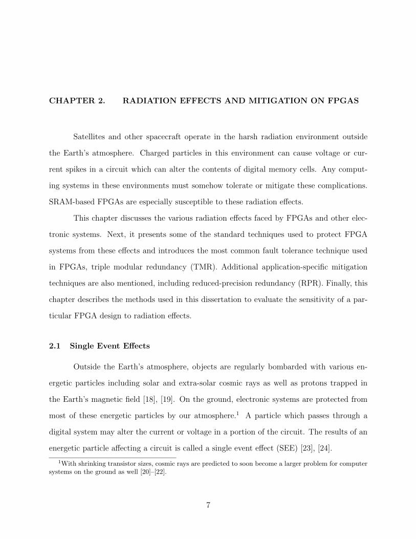
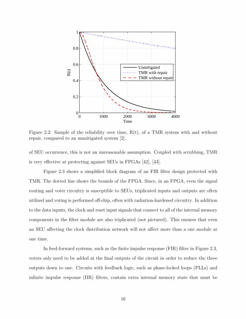
Figure 2.2 plots the reliability over time of a TMR system with and without repair, compared
to an unmitigated system [2]. The repair process vastly improves the reliability of TMR.
In an FPGA, TMR is often coupled with configuration scrubbing as the repair process.
To simplify analysis, this dissertation makes the assumption that the only a single SEU exists
in an FPGA at any one time. When the scrubbing rate is sufficiently higher than the rate
15
0 1000 2000 3000 40000
0.2
0.4
0.6
0.8
1
Time
R(t
)
UnmitigatedTMR with repairTMR without repair
Figure 2.2: Sample of the reliability over time, R(t), of a TMR system with and withoutrepair, compared to an unmitigated system [2].
of SEU occurrence, this is not an unreasonable assumption. Coupled with scrubbing, TMR
is very effective at protecting against SEUs in FPGAs [42], [43].
Figure 2.3 shows a simplified block diagram of an FIR filter design protected with
TMR. The dotted line shows the bounds of the FPGA. Since, in an FPGA, even the signal
routing and voter circuitry is susceptible to SEUs, triplicated inputs and outputs are often
utilized and voting is performed off-chip, often with radiation-hardened circuitry. In addition
to the data inputs, the clock and reset input signals that connect to all of the internal memory
components in the filter module are also triplicated (not pictured). This ensures that even
an SEU affecting the clock distribution network will not affect more than a one module at
one time.
In feed-forward systems, such as the finite impulse response (FIR) filter in Figure 2.3,
voters only need to be added at the final outputs of the circuit in order to reduce the three
outputs down to one. Circuits with feedback logic, such as phase-locked loops (PLLs) and
infinite impulse response (IIR) filters, contain extra internal memory state that must be
16

Figure 2.3: Simplified block diagram of an FIR filter protected with triple modular redun-dancy (TMR). The portion surrounded by the dotted box is implemented on the FPGA.
synchronized between the three circuit replicas. These more complicated circuits must also
have extra voter modules inserted within the feedback loops in each replicate to ensure that
memory state is maintained [44], [45]. Due to the triplication of the circuit and the addition
of voter modules, TMR has a hardware overhead of over 200%.
2.2.4 Application Specific Fault Tolerance
Due to the high cost of TMR, researchers have looked into alternative mitigation
strategies. In searching for alternatives to TMR, various authors have noted that reduced-
cost mitigation techniques might be obtained by using knowledge of the system in question.
These approaches, primarily targeting ASIC-based systems, have been called algorithm-
based fault tolerance (ABFT) [46], algorithmic soft error tolerance (ASET) [47], and system
knowledge [48].
Some authors have shown that the effects of soft errors in a DSP system can sometimes
be viewed as noise. Several papers have examined soft errors produced in ASICs by deep-
submicron (DSM) noise as well as those produced by using voltage overscaling (VOS) to
reduce power [4], [47], [49], [50]. Although this dissertation makes a similar analysis, the
17
effects of soft errors in ASICs are distinct from those which are of main concern for SRAM
FPGA systems as explained in Sections 2.1.2–2.1.4.
Others have published papers dealing with the effects of radiation-induced SEUs
in ASIC-based DSP systems [48], [51]–[53]. These papers focus on errors in the memory
elements of the systems, which is the dominant issue in ASIC technologies. In contrast, this
dissertation considers the effects of SEUs in any part of the FPGA configuration memory,
which specifies the logic implemented in addition to the user memory.
This dissertation evaluates reduced-precision redundancy (RPR) as an alternative
to TMR in FPGA-based DSP and communications systems. RPR was introduced as an
alternative to TMR for ASIC-based DSP systems [54]. RPR offers less protection than
TMR, but at a much lower cost. Chapter 4 will describe RPR in detail and Chapters 5 and
6 will present its application on FPGAs for SEU mitigation.
2.3 Evaluating FPGA Design Reliability
The reliability of an FPGA design can be assessed by experimentally determining
the effects of SEUs on the design. Evaluating the sensitivity of a design to SEUs allows the
designer to predict the failure rate of the design once deployed. A reliability assessment can
also be used to evaluate the effectiveness of a mitigation technique or to compare different
mitigation schemes. This section describes how fault injection experiments are used to
determine the effects of SEUs on an FPGA design and to predict the reliability of the
design.
2.3.1 Sensitivity
Each individual FPGA design has a distinct level of susceptibility to SEUs. The
FPGA configuration is made up of a large array of memory cells which control the hardware
implemented. For any particular FPGA design, however, only a fraction of these cells are
18
utilized. The FPGA fabric includes many different options for routing and logic configura-
tion. Even a design with “100%” logic utilization only uses a small percentage of the total
number of resources available since it does not make use of all of these options [55]–[57]. The
configuration cells which are utilized by a particular design are called the utilized bits of the
design.
A subset of the utilized configuration bits is the set of sensitive bits. Sensitive bits are
those which cause the output of the design to change when they are upset. For an unmitigated
design, the set of utilized bits and set of sensitive bits is the same. SEU mitigation applied to
a design may mask the errors caused by some upsets, resulting in some utilized bits which are
not sensitive to SEUs. The number and location of the sensitive bits is called the sensitivity
of the design [3].
2.3.2 Fault Injection Experiments
The utilized and sensitive bits of a particular FPGA design can be discovered through
fault injection experiments. Fault injection involves manually inserting faults into the config-
uration bitstream by changing the contents of individual memory cells. Using fault injection,
every configuration bit in the FPGA can be tested one by one to determine the utilization
and sensitivity of a particular design.
Several fault injection methods have been suggested for evaluating FPGA designs [3],
[32], [58]. Each of these methods alters the contents of the configuration memory and then
examines the output of the design for errors. The experiments presented in this dissertation
are based on the fault injection method presented in [3]. This method is described here and
will be extended in Section 3.1. Appendix A describes the specific hardware used for the
experiments presented in this dissertation.
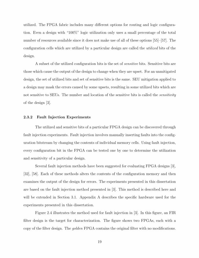
Figure 2.4 illustrates the method used for fault injection in [3]. In this figure, an FIR
filter design is the target for characterization. The figure shows two FPGAs, each with a
copy of the filter design. The golden FPGA contains the original filter with no modifications.
19
The design under test (DUT) FPGA contains the filter being tested by injecting faults in
the configuration. The two FPGAs receive identical input streams, in this case random bits,
and the outputs of the two chips are compared.
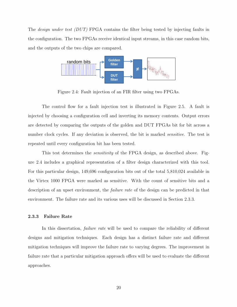
Figure 2.4: Fault injection of an FIR filter using two FPGAs.
The control flow for a fault injection test is illustrated in Figure 2.5. A fault is
injected by choosing a configuration cell and inverting its memory contents. Output errors
are detected by comparing the outputs of the golden and DUT FPGAs bit for bit across a
number clock cycles. If any deviation is observed, the bit is marked sensitive. The test is
repeated until every configuration bit has been tested.
This test determines the sensitivity of the FPGA design, as described above. Fig-
ure 2.4 includes a graphical representation of a filter design characterized with this tool.
For this particular design, 149,696 configuration bits out of the total 5,810,024 available in
the Virtex 1000 FPGA were marked as sensitive. With the count of sensitive bits and a
description of an upset environment, the failure rate of the design can be predicted in that
environment. The failure rate and its various uses will be discussed in Section 2.3.3.
2.3.3 Failure Rate
In this dissertation, failure rate will be used to compare the reliability of different
designs and mitigation techniques. Each design has a distinct failure rate and different
mitigation techniques will improve the failure rate to varying degrees. The improvement in
failure rate that a particular mitigation approach offers will be used to evaluate the different
approaches.
20

Figure 2.5: The exhaustive fault injection flow described in [3].
The failure rate, λ, of any system is so named because it describes the rate at which
failures occur in time. More precisely, λ is the number of expected failures in the system
per unit time. For random independent events such as SEUs, a constant failure rate is often
assumed which ignores effects such as wear-out and infant mortality [2].
The failure rate for a system, of course, depends on the definition of failure. Failure
may be defined in many ways including non-optimal operation, an error count above a certain
threshold, or as complete failure to operate. The definition of failure can have a great impact
on the reported failure rate of a system. This chapter defines failure in an FPGA design
as any deviation in the output from an SEU-free version of the design. In later chapters, a
more loose interpretation of failure will be used in some circumstances.
21

Failure Rate of an FPGA Design
The failure rate of an FPGA design due to SEUs is dependent upon the radiation
environment, the physical characteristics of the FPGA device, and the cross-section of (i.e.
the area taken up by) the design. The radiation environment defines the type, flux, and
energy of the charged particles in the environment. The flux is the rate at which the particles
flow through a certain area of space. The physical characteristics of the FPGA device define
how the radiation environment characteristics affect the rate of upset occurrence in the
FPGA fabric. The physical cross-section of the design determines the rate that SEUs occur
in that particular design.
Table 2.1 gives the expected upset rates for the Xilinx Virtex-4 FPGA family. The
device upset rates for low Earth orbit (LEO), polar orbit (Polar), and geosynchronous orbit
(GEO) for the Virtex-4 SX-55 device were obtained from [1]. This is a composite number of
upsets per device per day over several types of solar conditions. The configuration bit upset
rates are simply the device upset rates divided by the number of configuration memory cells
in the device and represent the number of configuration bits that are expected to be upset
per unit time in each radiation environment. In this dissertation, these rate will be taken as
constant upset rates for simplicity. Although upset rates may change over time even within
the same orbit (such as the increase in radiation when a satellite passes through the South
Atlantic Anomaly in a LEO orbit), such considerations are beyond the scope of this work.
Table 2.1: Orbit characteristics and composite upset ratesfor the Xilinx Virtex-4 SX-55 FPGA from [1].
Orbit InclinationDevice Configuration Bit
Altitude Upset Rate Upset Rate(km) SEUs/Device/s SEUs/bit/s
GEO 35,786 0◦ 3.46×10⁻³ 1.52×10⁻¹⁰
GPS 20,200 55◦ 3.03×10⁻³ 1.34×10⁻¹⁰
Molniya 39,305/1,507 63.2◦ 3.30×10⁻³ 1.45×10⁻¹⁰
Polar 833 98.7◦ 8.01×10⁻⁴ 3.53×10⁻¹¹
LEO 560 35.0◦ 2.16×10⁻⁵ 9.52×10⁻¹³
22

By combining the upset rate of the environment and the sensitivity of an FPGA
design, the failure rate can be predicted. The failure rate, λ, of an FPGA design is the
configuration bit upset rate multiplied by the number of sensitive configuration bits in a
particular FPGA design.
Sample Failure Rate Calculations
Table 2.2 shows the size and sensitivity of a small FIR filter design implemented
on a Virtex-4 SX-55 FPGA. For comparison, the first row of Table 2.2 shows the number
of FPGA “slice” resources and configuration bits available in the entire FPGA as if every
configuration bit were utilized and marked as sensitive. The second row of Table 2.2 indicates
that the FIR Filter design uses 2.9% of the slices in the FPGA device but only 0.189% of
the total configuration bits in the device are sensitive to SEUs. The third row shows these
same numbers for the FIR Filter design as protected with TMR. The TMR FIR Filter
design utilized roughly 3 times the amount of hardware as the original FIR Filter design, as
expected.
Table 2.2: Sensitivity of some simple designs and the Virtex-4 SX-55device on which they were implemented.
Target Slices Utilized Sensitive Bits
Entire Device 24,576 (100%) 22,702,848 (100%)FIR Filter 712 (2.90%) 42,978 (0.189%)
TMR FIR Filter 2,089 (8.50%) 2 (8.81×10⁻⁶%)
Table 2.3 gives the failure rates (λ) for each design based on the number of sensitive
bits and the configuration bit upset rate for each orbit. This table is simply the configu-
ration bit upset rates in Table 2.1 multiplied by the number of sensitive bits in Table 2.2.
Predictably, the failure rate of the FIR Filter design is much lower than that of the entire
device and the failure rate of the TMR filter is lower still.
Although TMR theoretically offers complete protection of the configuration memory,
the fault injection experiments revealed two configuration bits that were still susceptible to
23

Table 2.3: Failure rates (λ) in various orbits for some simple designs and the Virtex-4SX-55 device on which they were implemented. For the circuit designs,
these rates are based on the number of sensitive bits in the design.
Target GEO GPS Molniya Polar LEO
Entire Device 3.46×10⁻³ 3.03×10⁻³ 3.30×10⁻³ 8.01×10⁻⁴ 2.16×10⁻⁵
FIR Filter 6.55×10⁻⁶ 5.74×10⁻⁶ 6.25×10⁻⁶ 1.52×10⁻⁶ 4.09×10⁻⁸
TMR FIR Filter 3.05×10⁻¹⁰ 2.67×10⁻¹⁰ 2.91×10⁻¹⁰ 7.06×10⁻¹¹ 1.90×10⁻¹²
SEUs in the TMR design. This left the value of λ at slightly higher than zero in all cases, but
the improvement over the unmitigated design is clear. The failure rate of the TMR design
is over 21,000 times better than the original design.
Applications of Failure Rate
Failure rate can be used to describe the reliability of an FPGA design in several ways.
The raw failure rate of a design gives the number of expected failures per unit time. This
rate can also be used to compute other interesting characteristics of the design including
mean time to failure (MTTF), availability, and continuous time reliability. Each of these
measures may be used for different purposes in different applications.
The mean time to failure (MTTF) of a design is the expected time from initial
operation until a failure occurs. Assuming a constant failure rate in an unmitigated design,
MTTF is simply the inverse of that rate:
MTTF =1
λ. (2.1)
This is a useful quantity that may be easier to visualize than the raw failure rate since it
has units of time (rather than 1/time). For example, in the GPS orbit, the MTTF of the
sample FIR Filter design would be 174,216 seconds. Thus after beginning operation, this
small design would not be expected to be affected by an SEU for roughly 120 days. This
is only an expected value, of course. Failure could occur much sooner or later than this
estimate.
24
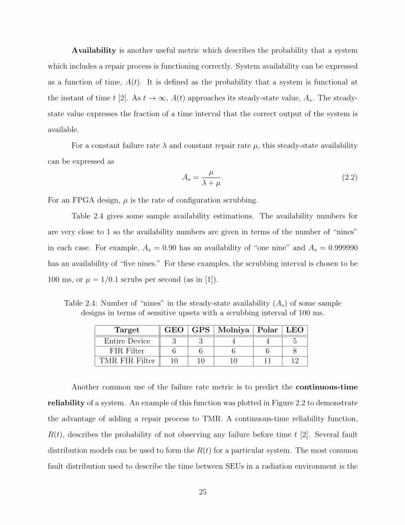
Availability is another useful metric which describes the probability that a system
which includes a repair process is functioning correctly. System availability can be expressed
as a function of time, A(t). It is defined as the probability that a system is functional at
the instant of time t [2]. As t→∞, A(t) approaches its steady-state value, As. The steady-
state value expresses the fraction of a time interval that the correct output of the system is
available.
For a constant failure rate λ and constant repair rate µ, this steady-state availability
can be expressed as
As =µ
λ+ µ. (2.2)
For an FPGA design, µ is the rate of configuration scrubbing.
Table 2.4 gives some sample availability estimations. The availability numbers for
are very close to 1 so the availability numbers are given in terms of the number of “nines”
in each case. For example, As = 0.90 has an availability of “one nine” and As = 0.999990
has an availability of “five nines.” For these examples, the scrubbing interval is chosen to be
100 ms, or µ = 1/0.1 scrubs per second (as in [1]).
Table 2.4: Number of “nines” in the steady-state availability (As) of some sampledesigns in terms of sensitive upsets with a scrubbing interval of 100 ms.
Target GEO GPS Molniya Polar LEO
Entire Device 3 3 4 4 5FIR Filter 6 6 6 6 8
TMR FIR Filter 10 10 10 11 12
Another common use of the failure rate metric is to predict the continuous-time
reliability of a system. An example of this function was plotted in Figure 2.2 to demonstrate
the advantage of adding a repair process to TMR. A continuous-time reliability function,
R(t), describes the probability of not observing any failure before time t [2]. Several fault
distribution models can be used to form the R(t) for a particular system. The most common
fault distribution used to describe the time between SEUs in a radiation environment is the
25
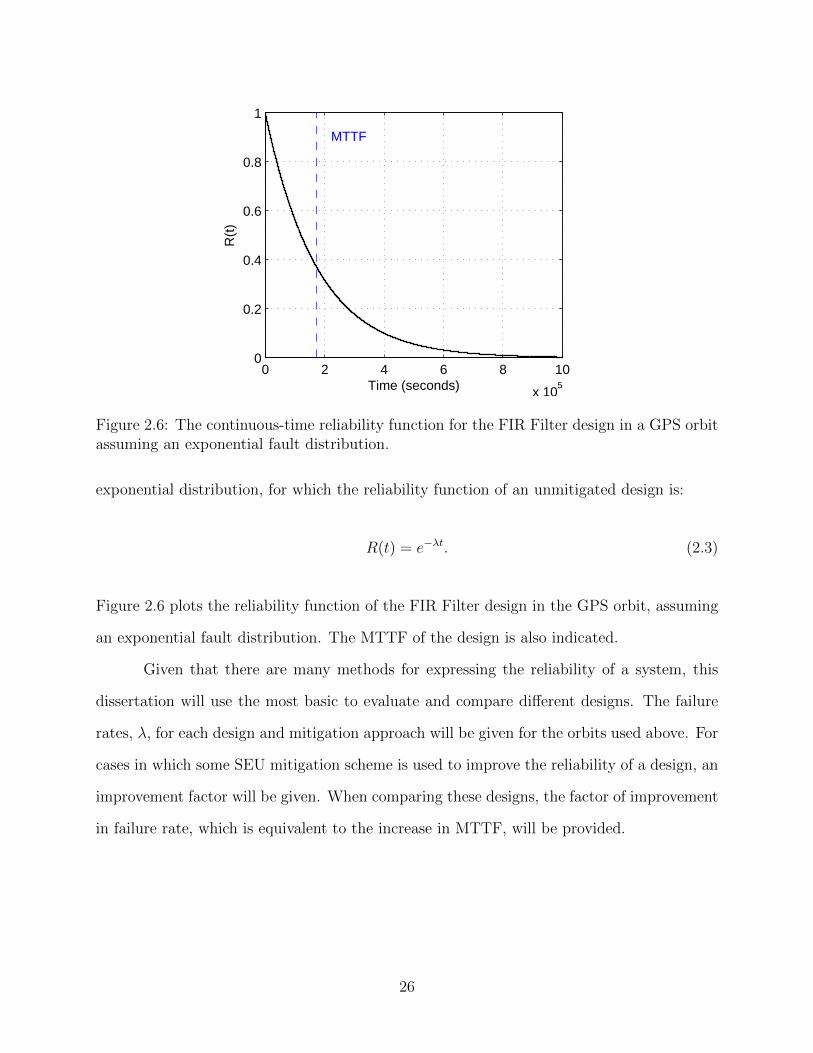
0 2 4 6 8 10
x 105
0
0.2
0.4
0.6
0.8
1
MTTF
Time (seconds)
R(t
)
Figure 2.6: The continuous-time reliability function for the FIR Filter design in a GPS orbitassuming an exponential fault distribution.
exponential distribution, for which the reliability function of an unmitigated design is:
R(t) = e−λt. (2.3)
Figure 2.6 plots the reliability function of the FIR Filter design in the GPS orbit, assuming
an exponential fault distribution. The MTTF of the design is also indicated.
Given that there are many methods for expressing the reliability of a system, this
dissertation will use the most basic to evaluate and compare different designs. The failure
rates, λ, for each design and mitigation approach will be given for the orbits used above. For
cases in which some SEU mitigation scheme is used to improve the reliability of a design, an
improvement factor will be given. When comparing these designs, the factor of improvement
in failure rate, which is equivalent to the increase in MTTF, will be provided.
26

2.4 Summary
SRAM-based FPGAs operating in space are susceptible to radiation-induced upsets
(SEUs) in their configuration memory array. These SEUs corrupt the data processed within
the FPGA as well as the function of the circuit implemented. The configuration memory is
the most significant source of SEU-induced errors due to its large size compared to the other
memory elements in an FPGA.
SEUs in the configuration memory are soft errors and can be repaired through con-
figuration scrubbing. Scrubbing can be combined with SEU mitigation techniques to mask
errors caused by SEUs. TMR, the most popular SEU mitigation technique for FPGAs, is
very effective but is expensive in terms of circuit area and power. Some alternative mitiga-
tion techniques have been suggested that are specific to a particular application domain and
have a lower cost than TMR.
The effectiveness of different mitigation techniques can be compared with fault in-
jection. Fault injection is an effective method for measuring the sensitivity of a particular
design to configuration SEUs. The failure rate derived from the fault injection results can be
used to predict the reliability and availability of a mitigated design in a particular radiation
environment.
Chapter 3 presents a novel fault injection method for evaluating DSP and communi-
cations systems for susceptibility to SEUs which measures performance loss instead of raw
sensitivity. Chapter 4 then presents RPR as an application-specific mitigation technique for
DSP communications systems using this new measure of performance and compares it with
TMR.
27

28
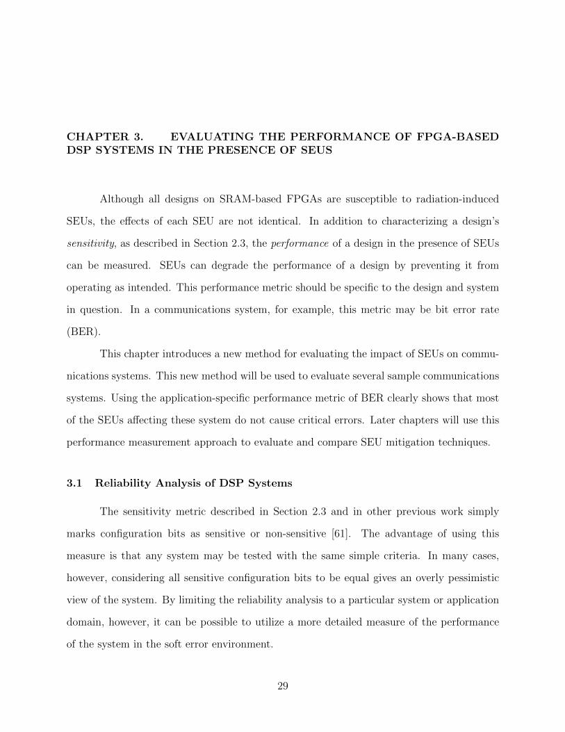
CHAPTER 3. EVALUATING THE PERFORMANCE OF FPGA-BASEDDSP SYSTEMS IN THE PRESENCE OF SEUS
Although all designs on SRAM-based FPGAs are susceptible to radiation-induced
SEUs, the effects of each SEU are not identical. In addition to characterizing a design’s
sensitivity, as described in Section 2.3, the performance of a design in the presence of SEUs
can be measured. SEUs can degrade the performance of a design by preventing it from
operating as intended. This performance metric should be specific to the design and system
in question. In a communications system, for example, this metric may be bit error rate
(BER).
This chapter introduces a new method for evaluating the impact of SEUs on commu-
nications systems. This new method will be used to evaluate several sample communications
systems. Using the application-specific performance metric of BER clearly shows that most
of the SEUs affecting these system do not cause critical errors. Later chapters will use this
performance measurement approach to evaluate and compare SEU mitigation techniques.
3.1 Reliability Analysis of DSP Systems
The sensitivity metric described in Section 2.3 and in other previous work simply
marks configuration bits as sensitive or non-sensitive [61]. The advantage of using this
measure is that any system may be tested with the same simple criteria. In many cases,
however, considering all sensitive configuration bits to be equal gives an overly pessimistic
view of the system. By limiting the reliability analysis to a particular system or application
domain, however, it can be possible to utilize a more detailed measure of the performance
of the system in the soft error environment.
29

(a)
(b)
Figure 3.1: (a) Model of a DSP system with an additive noise component and (b) the samesystem with an additional SEU-induced noise component.
In many DSP systems, processing is expected to be somewhat imprecise due to noise.
Noise in a data transmission channel corrupts the signals being processed. This noise is
often expressed in terms of the ratio of the signal power to the noise power, or signal-to-noise
ratio (SNR). With more noise added to the input signal of the system (a lower SNR), the
output tends to degrade further.
Analog signal processing systems carry with them the notion of a noise figure, the
measure of noise added to the system by the processing element itself. The noise figure is
defined as the difference between the output SNR and the input SNR (in decibels (dB)):
NF = 10 log
(SNRin
SNRout
)= SNRin,dB − SNRout,dB. (3.1)
In the presence of soft errors, the performance of a DSP system may degrade in a
similar manner to channel noise. In many instances, a DSP system corrupted by an SEU
may be thought of as having a noise figure, since the SEU adds “noise” to the system in a
similar way. Figure 3.1 compares a standard additive noise channel model (Figure 3.1(a))
with a model including this SEU-induced noise (Figure 3.1(b)).
30
0 2 4 6 8 10 12 14 16 1810
−8
10−7
10−6
10−5
10−4
10−3
10−2
10−1
100
Eb/N
o (dB)
BE
R
16−PSK8−PSKBPSK/QPSK
Figure 3.2: Bit error rate curves for several phase-shift keying (PSK) communications sys-tems with an AWGN channel.
3.2 Reliability Analysis of Communications Systems
This dissertation uses the digital communications application domain as a specific
example of a type of DSP system to be evaluated. Rather than using SNR to measure
performance, communications systems typically use bit error rate (BER), the number of
incorrectly-received bits in a signal divided by the total number of bits transferred.
The BER of a system is often reported as a function of the SNR, assuming an additive
white Gaussian noise (AWGN) channel. Gaussian noise is a often a product of the thermal
noise in the analog components of the communications system [62]. Figure 3.2 plots the effect
of different levels of noise for several phase-shift keying (PSK) communications systems. As
the noise in the communications channel decreases, increasing the SNR (Eb/N0), the BER
for each system decreases.
Communications systems are designed to tolerate some degree of noise. Although
the BER of such systems is theoretically directly related to the SNR (in an ideal AWGN
31
channel), the important metric in the end is the BER. Thus if a system is able to tolerate
some SEU-induced noise in addition to the Gaussian noise (or other type of noise) it was
designed for, the BER may remain low for these SEUs.
Having the ability to tolerate some SEU-induced noise would also mean that some
forms of SEU-induced noise may be ignored when developing an SEU mitigation approach.
As this chapter will show, the percentage of SEUs that can be mitigated by the inherent
noise handling of the communications systems can be quite high. This allows the use of
a mitigation approach that reduces overhead cost significantly by ignoring these types of
upsets. Thus rather than protecting the entire circuit with TMR, incurring 200% overhead
or more, only the most critical parts of the circuit may need to be protected: those in which
the SEUs have the most detrimental effect on the system performance. This protection could
be added using TMR selectively or using some other approach.
Section 3.5 will show that the different possible SEUs in an FPGA communications
system cause varying levels of noise. Those that cause lower levels of noise could be ignored
by a mitigation approach. That section will also identify the sections of our test circuits that
are most susceptible to high levels of noise with the intent of focusing a mitigation approach
on those most critical sections.
3.3 Application-Specific Fault Injection
Section 2.3.2 described a method for evaluating the sensitivity of a design to SEUs
using fault injection. Performing traditional sensitivity measurement using fault injection,
however, is pessimistic in nature for DSP systems. This form of fault injection assumes that
each configuration cell in the design is equally important. For DSP and Communications
systems, each SEU has a different effect on the output of the design. To measure these
differences, the application of the design must be accounted for.
For example, a DSP system could be evaluated in terms of the SNR loss at its output
instead of bitwise equality. Figure 3.3 shows an example of such a test system using a digital
32

Figure 3.3: A fault injection flow for general DSP systems.
Figure 3.4: A fault injection flow for communications systems.
filter as the test design. An identical set of input is fed to both a golden filter and a DUT
filter, in which faults are inserted. The output signal of each filter is recorded and the SNR
(in dB) of each is calculated. The difference between these SNR values is the noise figure
of the filter corrupted by that particular SEU. By testing every sensitive bit in the FPGA
design, a noise figure can be recorded for every possible SEU.
For a digital communications application, BER is the metric of interest. Figure 3.4
illustrates how a communications system could be tested. For each upset, a BER curve
similar to those in Figure 3.2 could be generated by sweeping the SNR of the signal at the
input to the FPGAs. The BER curve of the golden FPGA could then be compared to that of
the DUT FPGA for each upset. Thus the effect of every sensitive bit on the communications
system (not just the direct effect on the module being tested) can be determined.
33
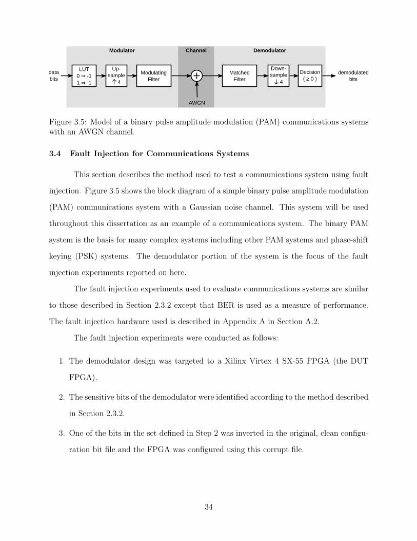
Figure 3.5: Model of a binary pulse amplitude modulation (PAM) communications systemswith an AWGN channel.
3.4 Fault Injection for Communications Systems
This section describes the method used to test a communications system using fault
injection. Figure 3.5 shows the block diagram of a simple binary pulse amplitude modulation
(PAM) communications system with a Gaussian noise channel. This system will be used
throughout this dissertation as an example of a communications system. The binary PAM
system is the basis for many complex systems including other PAM systems and phase-shift
keying (PSK) systems. The demodulator portion of the system is the focus of the fault
injection experiments reported on here.
The fault injection experiments used to evaluate communications systems are similar
to those described in Section 2.3.2 except that BER is used as a measure of performance.
The fault injection hardware used is described in Appendix A in Section A.2.
The fault injection experiments were conducted as follows:
1. The demodulator design was targeted to a Xilinx Virtex 4 SX-55 FPGA (the DUT
FPGA).
2. The sensitive bits of the demodulator were identified according to the method described
in Section 2.3.2.
3. One of the bits in the set defined in Step 2 was inverted in the original, clean configu-
ration bit file and the FPGA was configured using this corrupt file.
34

4. For this configuration upset, a bit error rate curve was generated by processing the
modulated signal from the FuncMon with the system defined by the corrupted config-
uration bit file.
5. For the non-catastrophic SEUs, the bit error rate curve produced by the previous step
was compared to the curve for the system in the absence of upsets. The performance
loss (in terms of SNR) is estimated by taking the difference of the SNR value of each
curve at a bit error rate of 10−5.
Steps 3–5 were repeated for each of the sensitive configuration bits, as defined in Step 2.
This process simulated the occurrence of all relevant SEUs, each being present one at a time
as expected in an FPGA system with a proper scrubbing system.
With this hardware-driven test with minimal communication with the host PC, the
BER tests for an entire design were able to run very rapidly. These tests measured bit error
rates down to 10−6 at SNR values of 2, 4, 6, 8, and 10 dB for every sensitive configuration
bit. For a filter design utilizing 50,000 configuration bits, these tests ran in about 18 hours.
For more details, see Appendix A.
This fault injection method is used in this as well as in future chapters. Sections 3.5
and 3.6 will show the results of using this application-specific method on feed-forward and
recursive communications systems, respectively. Chapters 4–5 will use this fault injection
method to evaluate and compare different SEU mitigation techniques.
3.5 Feed-forward System Experiments
This section reports on fault injection experiments run on a simple binary PAM
demodulator system. This demodulator design is shown in Figure 3.6. The matched filter
makes up the bulk of the system in terms of FPGA resources.1 To simplify the analysis of
the fault injection results, the filter was the only block implemented on the test FPGA.
1The downsample block is simply an enabled register and the decision block reads and inverts the MSBof the downsample block output as a comparison against zero in two’s complement arithmetic.
35

Figure 3.6: A high-level block diagram of the receiver system.
3.5.1 Experimental Configuration
A fault injection experiment with the method described in Section 3.4 was used to
examine the impact of SEUs on system performance for several versions of the matched
filter in Figure 3.6. In these experiments, the pulse shape of the modulating and matched
filters was the square-root raised-cosine (SRRC) pulse shape with excess bandwidth α using
Lp = 3 [63]. In each case, the matched filter operated at N = 4 samples/bit. Filter
implementations with 16-bit filter coefficients and 8-bit filter coefficients were examined.
The inputs and filter registers had the same bit-widths as the coefficients. Two filter designs
were considered:
• A direct form 1 FIR (finite impulse response) filter, as shown in Figure 3.7 (a), was
constructed directly from FPGA slices2.
• An alternative approach, based on the built-in DSP blocks of the Xilinx FPGA (called
“DSP48” blocks), was used to design a transposed direct form 1 FIR filter, as illustrated
in Figure 3.7 (b).
Six combinations of these design parameters were investigated:
• “16b logic α = 1.0” means the SRRC pulse shape with α = 1.0 using 16-bit inputs and
filter coefficients in the arrangement illustrated in Figure 3.7 (a).
• “16b logic α = 0.25” means the SRRC pulse shape with α = 0.25 using 16-bit inputs
and filter coefficients in the arrangement illustrated in Figure 3.7 (a).
2The hardware architecture used for this type of filter is illustrated in Figure C.1.
36
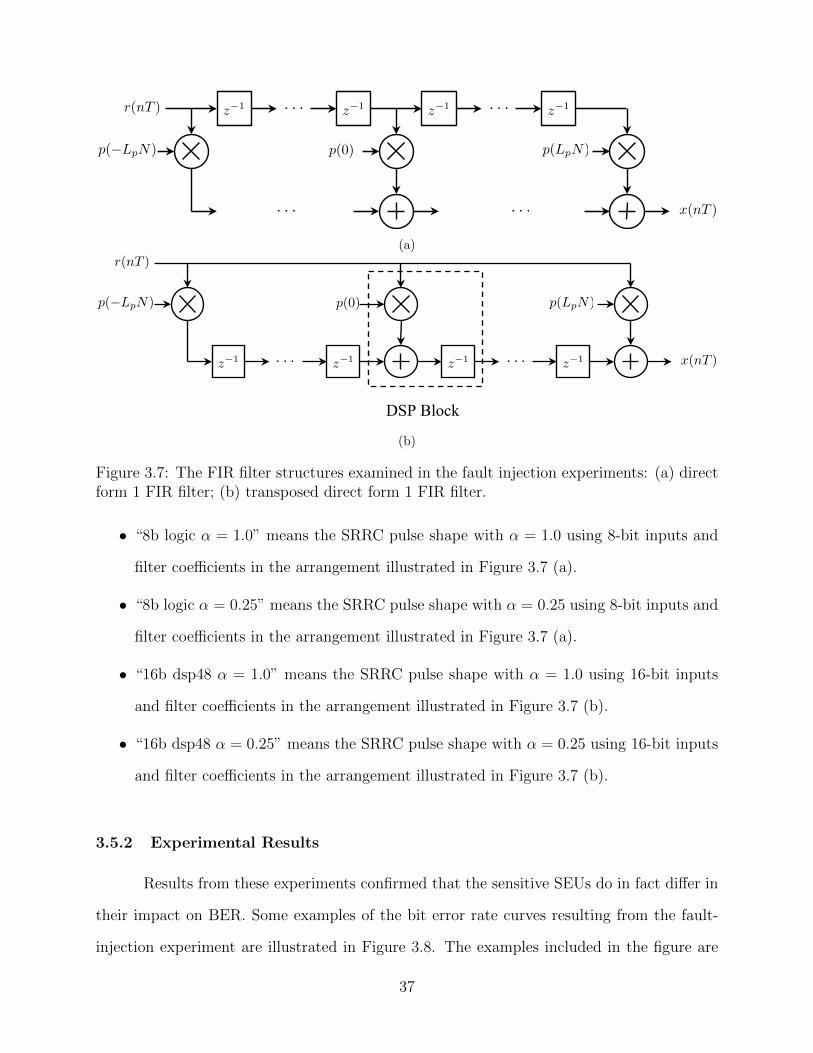
z−1
p(−LpN) p(LpN)p(0)
z−1 z−1z−1r(nT )
x(nT )
· · ·
· · ·
· · ·
· · ·
(a)
p(−LpN)
z−1
p(0)
z−1 z−1
p(LpN)
x(nT )z−1
r(nT )
DSP Block
· · · · · ·
(b)
Figure 3.7: The FIR filter structures examined in the fault injection experiments: (a) directform 1 FIR filter; (b) transposed direct form 1 FIR filter.
• “8b logic α = 1.0” means the SRRC pulse shape with α = 1.0 using 8-bit inputs and
filter coefficients in the arrangement illustrated in Figure 3.7 (a).
• “8b logic α = 0.25” means the SRRC pulse shape with α = 0.25 using 8-bit inputs and
filter coefficients in the arrangement illustrated in Figure 3.7 (a).
• “16b dsp48 α = 1.0” means the SRRC pulse shape with α = 1.0 using 16-bit inputs
and filter coefficients in the arrangement illustrated in Figure 3.7 (b).
• “16b dsp48 α = 0.25” means the SRRC pulse shape with α = 0.25 using 16-bit inputs
and filter coefficients in the arrangement illustrated in Figure 3.7 (b).
3.5.2 Experimental Results
Results from these experiments confirmed that the sensitive SEUs do in fact differ in
their impact on BER. Some examples of the bit error rate curves resulting from the fault-
injection experiment are illustrated in Figure 3.8. The examples included in the figure are
37
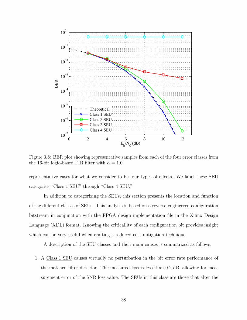
0 2 4 6 8 10 1210
−7
10−6
10−5
10−4
10−3
10−2
10−1
100
Eb/N
0 (dB)
BE
R
TheoreticalClass 1 SEUClass 2 SEUClass 3 SEUClass 4 SEU
Figure 3.8: BER plot showing representative samples from each of the four error classes fromthe 16-bit logic-based FIR filter with α = 1.0.
representative cases for what we consider to be four types of effects. We label these SEU
categories “Class 1 SEU” through “Class 4 SEU.”
In addition to categorizing the SEUs, this section presents the location and function
of the different classes of SEUs. This analysis is based on a reverse-engineered configuration
bitstream in conjunction with the FPGA design implementation file in the Xilinx Design
Language (XDL) format. Knowing the criticallity of each configuration bit provides insight
which can be very useful when crafting a reduced-cost mitigation technique.
A description of the SEU classes and their main causes is summarized as follows:
1. A Class 1 SEU causes virtually no perturbation in the bit error rate performance of
the matched filter detector. The measured loss is less than 0.2 dB, allowing for mea-
surement error of the SNR loss value. The SEUs in this class are those that alter the
38

memory cells defining the low-order bits of the filter coefficients, the low-order bits of
the outputs of the arithmetic units (i.e. the addition and multiplication blocks), etc.
2. A Class 2 SEU degrades the bit error rate performance in the same way an additional
source of additive noise degrades performance. This effect can be thought of as either an
implementation loss or, as mentioned earlier, as a noise figure. Class 2 SEUs are those
that impact the memory cells defining the middle-order bits of the filter coefficients,
the middle-order bits of the outputs of the arithmetic units, etc.
3. A Class 3 SEU produces an unusably high bit error rate floor.3 SEUs impacting the
memory cells that define the high-order bits in the filter coefficients, the high-order
bits in the outputs of the arithmetic units, etc. are the main causes of SEUs in this
category. These SEUs are considered catastrophic.
4. A Class 4 SEU produces a bit error rate of 1/2. These SEUs are also catastrophic and
are caused by faults in the memory cells defining the clock distribution network, the
global reset signal, the most significant bits (MSBs) of the matched filter output, etc.
The number of SEUs in each class is a function of the properties of the filter coefficients
(controlled in these experiments using the excess bandwidth parameter, α), the number of
bits used to quantify the filter coefficients, and the degree to which built-in units such as the
DSP48 blocks are used.
Graphical representations of the impact of all SEUs on the six designs used in the fault
injection experiments are shown in Figures 3.9 – 3.14. For each design, five fault injection
tests were run for input SNR values of 2, 4, 6, 8, and 10 dB. Each plot shows five histograms
corresponding to each of these tests. Each histogram shows the BER values measured for
3Note that our simulations ran only long enough to estimate bit error rates greater than 10−6 with anyuseful fidelity. It could be the case that many of the Class 2 SEUs really do have a bit error rate floorsomewhere below 10−6. A case could be made that these Class 2 SEUs should be Class 3 SEUs. Given thefact that most modern digital communication system use some form of error control coding and that anyuseful error correcting code can easily correct random errors at the rate of 10−6 or less, there is little meritin determining if such low bit error rate floors exist.
39
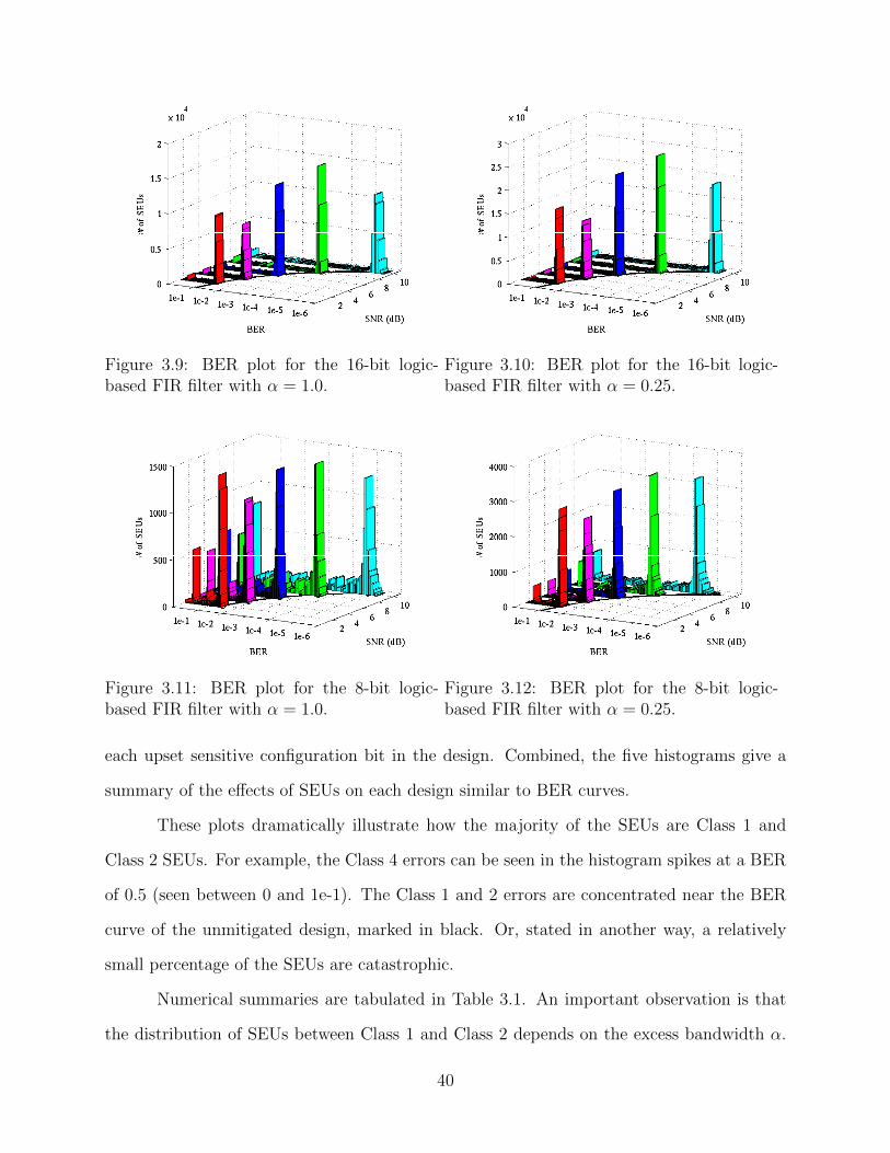
Figure 3.9: BER plot for the 16-bit logic-based FIR filter with α = 1.0.
Figure 3.10: BER plot for the 16-bit logic-based FIR filter with α = 0.25.
Figure 3.11: BER plot for the 8-bit logic-based FIR filter with α = 1.0.
Figure 3.12: BER plot for the 8-bit logic-based FIR filter with α = 0.25.
each upset sensitive configuration bit in the design. Combined, the five histograms give a
summary of the effects of SEUs on each design similar to BER curves.
These plots dramatically illustrate how the majority of the SEUs are Class 1 and
Class 2 SEUs. For example, the Class 4 errors can be seen in the histogram spikes at a BER
of 0.5 (seen between 0 and 1e-1). The Class 1 and 2 errors are concentrated near the BER
curve of the unmitigated design, marked in black. Or, stated in another way, a relatively
small percentage of the SEUs are catastrophic.
Numerical summaries are tabulated in Table 3.1. An important observation is that
the distribution of SEUs between Class 1 and Class 2 depends on the excess bandwidth α.
40

Figure 3.13: BER plot for the 16-bit DSP48-based FIR filter with α = 1.0.
Figure 3.14: BER plot for the 16-bit DSP48-based FIR filter with α = 0.25.
This is due to the fact that when α = 1.0, almost half of the filter coefficients are very close
to 0. In fact, when 8-bit coefficients are used, these small filter coefficients are quantized to 0.
The FPGA synthesis tools are smart enough to recognize that “multiplication by 0 followed
by accumulation” is unnecessary and does not devote any resources to this operation. When
α = 0.25, most of the filter coefficients are sufficiently non-zero to survive quantization.
Hence, the shortcut is not available to the synthesis tools and FPGA resources are devoted
to the computation. The number of FPGA slices used as well as the total number of utilized
bits in the design are larger for the α = 0.25 design than for the corresponding α = 1.0 design.
Interestingly, the percentage of non-catastrophic SEUs remains approximately constant.
The SEUs may also be quantified by the SNR loss they cause. These results are
summarized in Table 3.2. These data define a cumulative distribution of the SNR loss4 for
each of the 6 designs. As an example, consider the designs using 16 bit filter coefficients
with the filter structure of Figure 3.7 (a). Approximately 14% of all possible SEUs lead to
an SNR loss in excess of 1 dB. In other words, 86% of all sensitive SEUs give an SNR loss
less than 1 dB. The consequence of this observation is significant. If a 1 dB SNR loss is
acceptable, only 14% of the SEUs need to be targeted for mitigation. This represents a huge
potential savings in FPGA resources.
4Note that Class 3 and Class 4 SEUs have infinite SNR loss and are included in the percentages shown.
41

Table 3.1: Number of SEUs causing each class of effect for several designs.
TotalSlices/ Class 1 Class 2 Class 3 Class 4 Utilized Total
Design DSP48s Bits Bits Bits Bits Bits Cat. Bits
16b logicα = 1.0
712/034,829 5,612 1,638 899
42,9782,537
(81%) (13%) (3.8%) (2.1%) (5.90%)16b logicα = 0.25
1,029/050,798 14,479 2,908 1,022
69,2073,930
(73%) (21%) (4.2%) (1.5%) (5.68%)8b logicα = 1.0
194/03,158 4,914 768 841
9,6811,609
(33%) (51%) (7.9%) (8.7%) (16.62%)8b logicα = 0.25
297/02,210 12,445 1,816 908
17,7792,724
(12%) (70%) (10%) (5.1%) (15.32%)16b dsp48α = 1.0
554/1322,047 5,498 867 1,118
29,5301,985
(75%) (19%) (2.9%) (3.8%) (6.72%)16b dsp48α = 0.25
554/1324,140 13,861 1,263 1,031
40,2952,294
(60%) (34%) (3.1%) (2.6%) (5.69%)
Table 3.2: Percentage of SEUs causing certain SNR losses at BER of 10−5.
Design > 0.2 dB > 0.5 dB > 1 dB > 3 dB > 6 dB
16b logic α = 1.0 18.96% 16.37% 14.32% 11.20% 9.21%
16b logic α = 0.25 26.60% 17.39% 14.36% 10.58% 9.08%
8b logic α = 1.0 67.38% 51.93% 43.65% 33.33% 26.20%
8b logic α = 0.25 85.32% 45.27% 37.19% 27.92% 24.11%
16b dsp48 α = 1.0 25.34% 22.13% 20.18% 15.92% 12.05%
16b dsp48 α = 0.25 40.09% 22.54% 18.40% 13.69% 10.92%
The situation is less dramatic for the design based on 8-bit filter coefficients. This
is because a higher percentage of the filter coefficient bits are significant in terms of how
much they contribute to the output of the filter. These coefficients are the same as the
16-bit filters, but half of the lower-order (and less significant) bits have been truncated. As a
result, the Class 2 SEUs are associated with higher SNR losses relative to the corresponding
16-bit designs and a larger percentage of the SEUs are Class 3 SEUs.
3.5.3 Application-Specific Failure Rate
Using this fault injection data, the failure rate numbers in Section 2.3.3 can be up-
dated for this specific application. The failure rate of a system, of course, depends on the
42
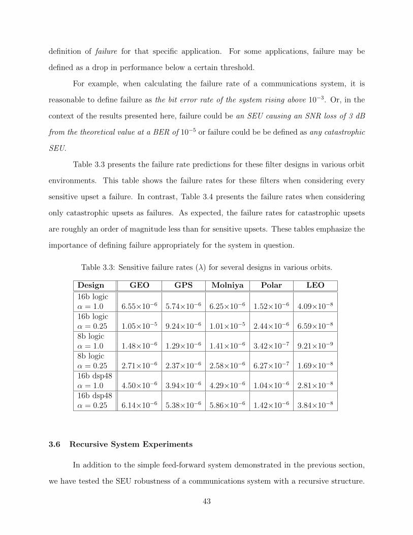
definition of failure for that specific application. For some applications, failure may be
defined as a drop in performance below a certain threshold.
For example, when calculating the failure rate of a communications system, it is
reasonable to define failure as the bit error rate of the system rising above 10−3. Or, in the
context of the results presented here, failure could be an SEU causing an SNR loss of 3 dB
from the theoretical value at a BER of 10−5 or failure could be be defined as any catastrophic
SEU.
Table 3.3 presents the failure rate predictions for these filter designs in various orbit
environments. This table shows the failure rates for these filters when considering every
sensitive upset a failure. In contrast, Table 3.4 presents the failure rates when considering
only catastrophic upsets as failures. As expected, the failure rates for catastrophic upsets
are roughly an order of magnitude less than for sensitive upsets. These tables emphasize the
importance of defining failure appropriately for the system in question.
Table 3.3: Sensitive failure rates (λ) for several designs in various orbits.
Design GEO GPS Molniya Polar LEO
16b logicα = 1.0 6.55×10⁻⁶ 5.74×10⁻⁶ 6.25×10⁻⁶ 1.52×10⁻⁶ 4.09×10⁻⁸
16b logicα = 0.25 1.05×10⁻⁵ 9.24×10⁻⁶ 1.01×10⁻⁵ 2.44×10⁻⁶ 6.59×10⁻⁸
8b logicα = 1.0 1.48×10⁻⁶ 1.29×10⁻⁶ 1.41×10⁻⁶ 3.42×10⁻⁷ 9.21×10⁻⁹
8b logicα = 0.25 2.71×10⁻⁶ 2.37×10⁻⁶ 2.58×10⁻⁶ 6.27×10⁻⁷ 1.69×10⁻⁸
16b dsp48α = 1.0 4.50×10⁻⁶ 3.94×10⁻⁶ 4.29×10⁻⁶ 1.04×10⁻⁶ 2.81×10⁻⁸
16b dsp48α = 0.25 6.14×10⁻⁶ 5.38×10⁻⁶ 5.86×10⁻⁶ 1.42×10⁻⁶ 3.84×10⁻⁸
3.6 Recursive System Experiments
In addition to the simple feed-forward system demonstrated in the previous section,
we have tested the SEU robustness of a communications system with a recursive structure.
43

Table 3.4: Catastrophic failure rates (λ) for several designs in various orbits.
Design GEO GPS Molniya Polar LEO
16b logicα = 1.0 3.87×10⁻⁷ 3.39×10⁻⁷ 3.69×10⁻⁷ 8.95×10⁻⁸ 2.41×10⁻⁹
16b logicα = 0.25 5.99×10⁻⁷ 5.25×10⁻⁷ 5.71×10⁻⁷ 1.39×10⁻⁷ 3.74×10⁻⁹
8b logicα = 1.0 2.45×10⁻⁷ 2.15×10⁻⁷ 2.34×10⁻⁷ 5.68×10⁻⁸ 1.53×10⁻⁹
8b logicα = 0.25 4.15×10⁻⁷ 3.64×10⁻⁷ 3.96×10⁻⁷ 9.61×10⁻⁸ 2.59×10⁻⁹
16b dsp48α = 1.0 3.03×10⁻⁷ 2.65×10⁻⁷ 2.89×10⁻⁷ 7.01×10⁻⁸ 1.89×10⁻⁹
16b dsp48α = 0.25 3.50×10⁻⁷ 3.06×10⁻⁷ 3.33×10⁻⁷ 8.10×10⁻⁸ 2.18×10⁻⁹
This type of test is significant because recursive (or feedback) systems often have more
complex error dynamics than feed-forward systems. This test was intended to determine if
the conclusions from the previous section would hold for a recursive system as well. This
section presents the experimental results from fault injection on a binary PAM receiver
with a symbol timing synchronization phased-locked loop (PLL). The full receiver system is
pictured in Figure 3.15.
Figure 3.15: Block diagram of the binary PAM demodulator with timing synchronization.
44
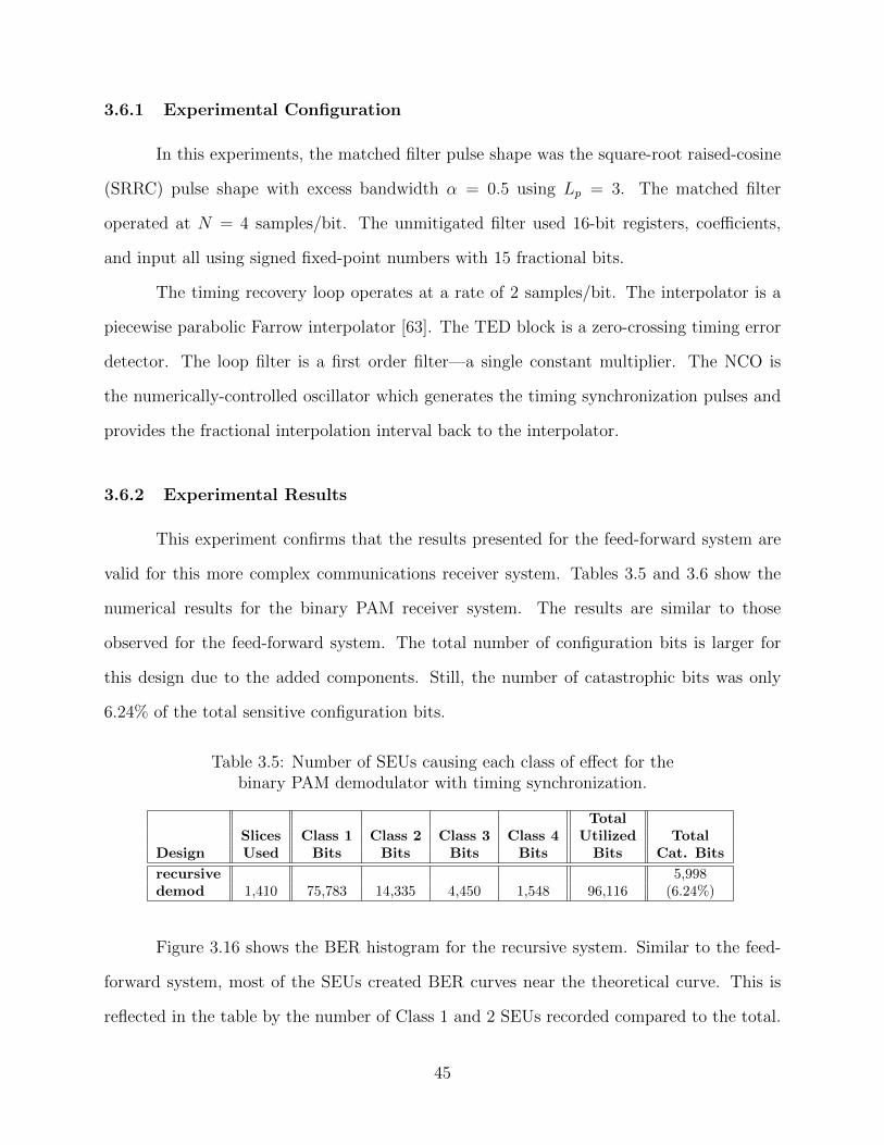
3.6.1 Experimental Configuration
In this experiments, the matched filter pulse shape was the square-root raised-cosine
(SRRC) pulse shape with excess bandwidth α = 0.5 using Lp = 3. The matched filter
operated at N = 4 samples/bit. The unmitigated filter used 16-bit registers, coefficients,
and input all using signed fixed-point numbers with 15 fractional bits.
The timing recovery loop operates at a rate of 2 samples/bit. The interpolator is a
piecewise parabolic Farrow interpolator [63]. The TED block is a zero-crossing timing error
detector. The loop filter is a first order filter—a single constant multiplier. The NCO is
the numerically-controlled oscillator which generates the timing synchronization pulses and
provides the fractional interpolation interval back to the interpolator.
3.6.2 Experimental Results
This experiment confirms that the results presented for the feed-forward system are
valid for this more complex communications receiver system. Tables 3.5 and 3.6 show the
numerical results for the binary PAM receiver system. The results are similar to those
observed for the feed-forward system. The total number of configuration bits is larger for
this design due to the added components. Still, the number of catastrophic bits was only
6.24% of the total sensitive configuration bits.
Table 3.5: Number of SEUs causing each class of effect for thebinary PAM demodulator with timing synchronization.
TotalSlices Class 1 Class 2 Class 3 Class 4 Utilized Total
Design Used Bits Bits Bits Bits Bits Cat. Bits
recursive 5,998demod 1,410 75,783 14,335 4,450 1,548 96,116 (6.24%)
Figure 3.16 shows the BER histogram for the recursive system. Similar to the feed-
forward system, most of the SEUs created BER curves near the theoretical curve. This is
reflected in the table by the number of Class 1 and 2 SEUs recorded compared to the total.
45
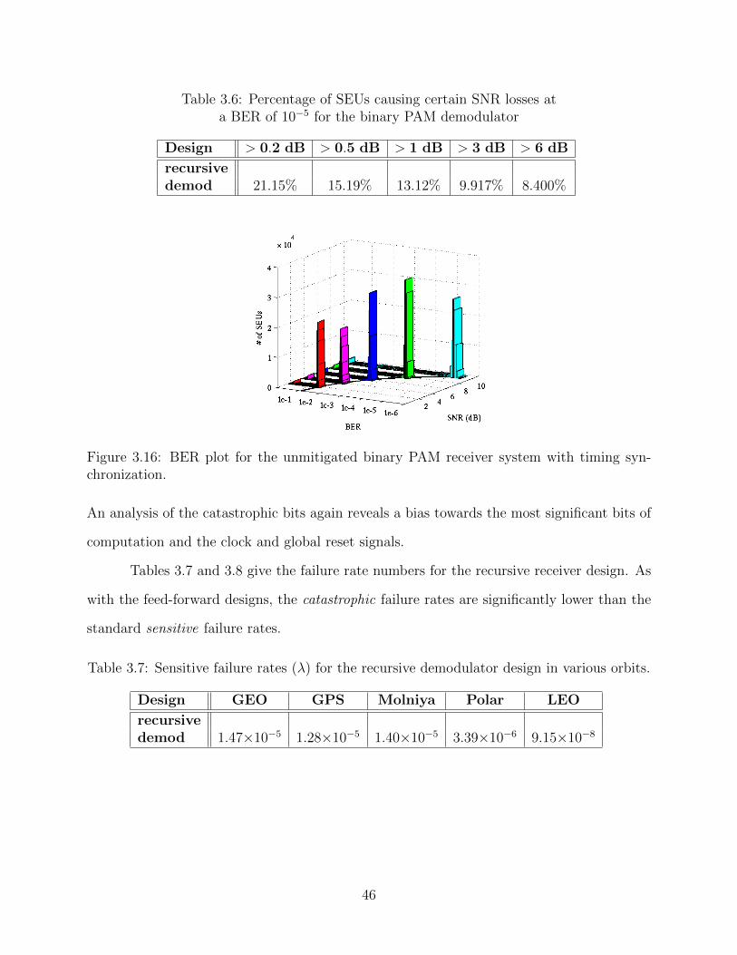
Table 3.6: Percentage of SEUs causing certain SNR losses ata BER of 10−5 for the binary PAM demodulator
Design > 0.2 dB > 0.5 dB > 1 dB > 3 dB > 6 dB
recursivedemod 21.15% 15.19% 13.12% 9.917% 8.400%
Figure 3.16: BER plot for the unmitigated binary PAM receiver system with timing syn-chronization.
An analysis of the catastrophic bits again reveals a bias towards the most significant bits of
computation and the clock and global reset signals.
Tables 3.7 and 3.8 give the failure rate numbers for the recursive receiver design. As
with the feed-forward designs, the catastrophic failure rates are significantly lower than the
standard sensitive failure rates.
Table 3.7: Sensitive failure rates (λ) for the recursive demodulator design in various orbits.
Design GEO GPS Molniya Polar LEO
recursivedemod 1.47×10⁻⁵ 1.28×10⁻⁵ 1.40×10⁻⁵ 3.39×10⁻⁶ 9.15×10⁻⁸
46

Table 3.8: Catastrophic failure rates (λ) for the recursivedemodulator design in various orbits.
Design GEO GPS Molniya Polar LEO
recursivedemod 9.14×10⁻⁷ 8.01×10⁻⁷ 8.72×10⁻⁷ 2.12×10⁻⁷ 5.71×10⁻⁹
3.7 Summary
This chapter presented an application-specific method for evaluating the impact of
SEUs on FPGA-based communications systems. The experimental results confirm that it
can be very useful to consider the specific application in question when measuring a design’s
performance in the presence of SEUs.
The experiments suggest that not all SEUs need to be targeted for mitigation in
an FPGA design subject to SEUs, depending on the design and application. This desirable
result follows the fact that the figure of merit is bit error rate (rather than bit-level accuracy)
and that the majority of the SEUs have the same effect as additive noise. Analysis of the
experimental data showed that the sections that must be protected from SEUs are the clock
distribution networks, global reset, and the MSBs of the arithmetic modules.
Because not all SEUs cause critical errors, mitigation techniques with much lower
cost are possible. For example, one might use TMR to protect only the upper bits of
the arithmetic modules, leaving the lower bits unprotected. This type of approach may
substantially reduce the resources required to produce a reliable system. Chapter 4 will
describe a mitigation technique that can be used for this purpose.
47

48
CHAPTER 4. REDUCED PRECISION REDUNDANCY
With the knowledge that few SEUs cause critical errors in a communications system
and knowing which portions of the circuit to protect, a reduced-cost mitigation approach can
be suggested. The ideal candidate protects the clock, global reset, and the most significant
bits of computation while possibly ignoring the least significant bits in order to mitigate
critical SEUs at a lower cost than TMR.
This chapter provides background on reduced-precision redundancy (RPR), a reduced-
cost mitigation technique designed to protect arithmetic computation. RPR focuses on pro-
tecting the most significant bits of computation, those which were found in Chapter 3 to
be associated with catastrophic SEUs. RPR can also be implemented such that the global
clock and reset signals are protected as well. With this focus, RPR is a good candidate for
reducing the cost of SEU mitigation on FPGA-based DSP systems.
This chapter describes the mechanics of RPR, the various operating modes of an
RPR system in the presence of SEUs, and a discusses the size vs. performance of RPR. It
lays the groundwork for a comparison of different RPR techniques which will be presented
in Chapter 5. The chapter concludes with an initial demonstration of RPR on the simple
communications system designs of Section 3.5. Fault injection experiments show that RPR
is well-suited to protect against the most critical SEUs at a much lower cost than TMR.
4.1 Previous Work
RPR was introduced by Shim, et al. as part of a power reduction technique for
ASIC-based DSP systems [4], [54]. Shim used RPR to overcome errors introduced by voltage
overscaling (VOS), which reduces the supply voltage of a circuit to save power. This voltage
49

reduction slows the operation of the circuit and can cause intermittent errors at the circuit
output when the longer logic paths are excited. RPR was used to reduce the effects of these
intermittent errors, which had the tendency to occur in the most significant bits of the circuit
output since those generally correspond to the longer paths through the logic. Shim’s version
of RPR is referred to as Threshold RPR in this dissertation.
Shim later modified this RPR technique and analyzed it as a means for protecting
against deep-submicron noise and soft errors in ASIC-based DSP systems [47]. This mod-
ification of RPR is more suited towards SEU mitigation for FPGAs than the original. In
a radiation environment, SEUs are distributed uniformly across an FPGA similar to soft
errors in ASIC systems. These errors are not biased towards the most significant bits as in
the VOS case. Still, because SEUs may impact the logic implemented by the FPGA, soft
errors in ASIC systems tend to be less severe than those of concern in FPGAs.
Snodgrass presented an alternate RPR configuration (called Bounded RPR in this
dissertation) and demonstrated it on FPGAs in [5]. Sullivan later provided details on how
to implement Bounded RPR on several elementary arithmetic operations and characterized
the performance of some RPR systems in simulation [64]. Both of these authors confirmed
that RPR could be a valuable SEU mitigation technique for certain FPGA-based systems.
This dissertation expands on previous work regarding RPR in several ways. Fault
injection experiments in this chapter and in Chapters 5–6 make direct comparisons of RPR
with TMR, clearly showing their costs and benefits. Chapter 5 compares several variations of
RPR, including those suggested by Shim and Snodgrass, in order to determine the best option
for FPGA implementation. Chapter 6 then presents methods to optimize the application of
RPR on communications systems and demonstrates how to apply RPR to complex systems
which are not completely suited to RPR.
50
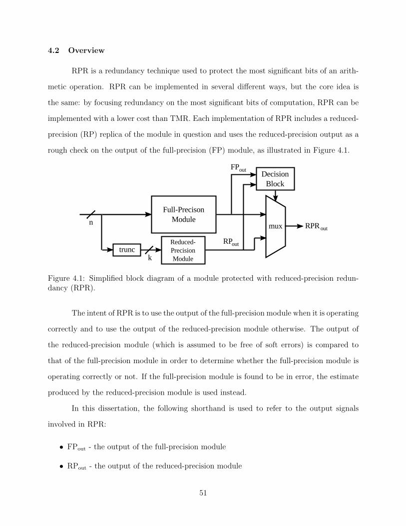
4.2 Overview
RPR is a redundancy technique used to protect the most significant bits of an arith-
metic operation. RPR can be implemented in several different ways, but the core idea is
the same: by focusing redundancy on the most significant bits of computation, RPR can be
implemented with a lower cost than TMR. Each implementation of RPR includes a reduced-
precision (RP) replica of the module in question and uses the reduced-precision output as a
rough check on the output of the full-precision (FP) module, as illustrated in Figure 4.1.
Figure 4.1: Simplified block diagram of a module protected with reduced-precision redun-dancy (RPR).
The intent of RPR is to use the output of the full-precision module when it is operating
correctly and to use the output of the reduced-precision module otherwise. The output of
the reduced-precision module (which is assumed to be free of soft errors) is compared to
that of the full-precision module in order to determine whether the full-precision module is
operating correctly or not. If the full-precision module is found to be in error, the estimate
produced by the reduced-precision module is used instead.
In this dissertation, the following shorthand is used to refer to the output signals
involved in RPR:
• FPout - the output of the full-precision module
• RPout - the output of the reduced-precision module
51

• FPtrue - the ideal (full-precision) output
• RPRout - the output of the RPR module as a whole
The core functionality of RPR is summarized as follows:
if FPout ≈ RPout then
RPRout ← FPout
else
RPRout ← RPout
end if,
where the specifics of the approximation operation are dependent on the RPR implemen-
tation. The difference between the RPRout signal and the desired FPtrue signal is the error
signal, εRPR, of the RPR module. The error of the RPR module, then, is defined as
εRPR = FPtrue − RPRout. (4.1)
RPR can be operating in three different modes: full-precision perfect, full-precision
degraded, and reduced-precision.
• In full-precision perfect mode, there are no upsets in the FP module and the output of
the system is the correct full-precision output. In this case, εRPR = 0.
• In full-precision degraded mode, the FP module is not operating perfectly, but its output
is still approximately equal to the reduced-precision output, so the slightly-degraded
FP output is used. In this case, εRPR = FPtrue − FPout.
• In reduced-precision mode, the FP module output is different enough from the RP
output to determine that there is an error in the FP module and the RP output is
used instead of the erroneous FP output. In this case, εRPR = FPtrue − RPout.
In Shim’s initial implementation of RPR, the reduced-precision module was small
enough to avoid the VOS errors which affected the full-precision module, which were his
52
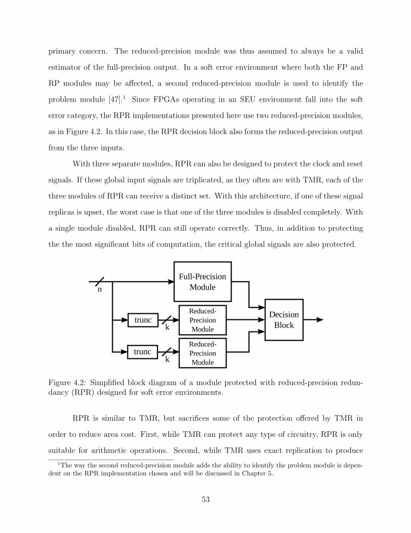
primary concern. The reduced-precision module was thus assumed to always be a valid
estimator of the full-precision output. In a soft error environment where both the FP and
RP modules may be affected, a second reduced-precision module is used to identify the
problem module [47].1 Since FPGAs operating in an SEU environment fall into the soft
error category, the RPR implementations presented here use two reduced-precision modules,
as in Figure 4.2. In this case, the RPR decision block also forms the reduced-precision output
from the three inputs.
With three separate modules, RPR can also be designed to protect the clock and reset
signals. If these global input signals are triplicated, as they often are with TMR, each of the
three modules of RPR can receive a distinct set. With this architecture, if one of these signal
replicas is upset, the worst case is that one of the three modules is disabled completely. With
a single module disabled, RPR can still operate correctly. Thus, in addition to protecting
the the most significant bits of computation, the critical global signals are also protected.
Figure 4.2: Simplified block diagram of a module protected with reduced-precision redun-dancy (RPR) designed for soft error environments.
RPR is similar to TMR, but sacrifices some of the protection offered by TMR in
order to reduce area cost. First, while TMR can protect any type of circuitry, RPR is only
suitable for arithmetic operations. Second, while TMR uses exact replication to produce
1The way the second reduced-precision module adds the ability to identify the problem module is depen-dent on the RPR implementation chosen and will be discussed in Chapter 5.
53

an error-free output, RPR uses smaller reduced-precision modules to limit the output error.
RPR has an advantage over TMR when it is able to sufficiently limit the magnitude of the
SEU-induced noise at a lower hardware cost.
The following sections will elaborate on these two points. Section 4.3 explains the
suitability of RPR for protecting arithmetic circuits. Section 4.4 presents the operating
modes of RPR along with a description of the general error bounds for each mode.
4.3 Protecting Arithmetic
As mentioned above, RPR is designed to protect arithmetic operations. Arithmetic
operations have a natural ordering and weighting of data with the more significant bits
located to the left of a vector of bits. In general, digital logic is not organized in this manner
and the relative significance of different portions of a circuit is not clear. The natural ordering
of arithmetic operations allows RPR to focus on the most important sections of a circuit.
The numeric operands of arithmetic modules are naturally ordered by their signifi-
cance. For these operations, the bits in a data word are arranged in descending weight from
the most significant bit (MSB) to the least significant bit (LSB). For example, an unsigned
binary number is represented as
bNbN−1...b1b0, (4.2)
bN being the MSB and b0 being the LSB. This binary representation is interpreted as
N∑i=0
bi2i. (4.3)
Thus the bits on the left have a larger value and are more significant than the bits on the
right.
A mitigation technique might exploit this property by giving priority to the upper
bits of the number since those have the greatest value. The simplest demonstration of this
concept in hardware is a register holding a binary number. Each flip-flop (FF) in the register
54
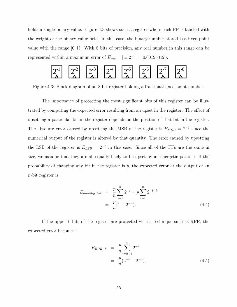
holds a single binary value. Figure 4.3 shows such a register where each FF is labeled with
the weight of the binary value held. In this case, the binary number stored is a fixed-point
value with the range [0, 1). With 8 bits of precision, any real number in this range can be
represented within a maximum error of Ereg = | ± 2−9| = 0.001953125.
Figure 4.3: Block diagram of an 8-bit register holding a fractional fixed-point number.
The importance of protecting the most significant bits of this register can be illus-
trated by computing the expected error resulting from an upset in the register. The effect of
upsetting a particular bit in the register depends on the position of that bit in the register.
The absolute error caused by upsetting the MSB of the register is EMSB = 2−1 since the
numerical output of the register is altered by that quantity. The error caused by upsetting
the LSB of the register is ELSB = 2−8 in this case. Since all of the FFs are the same in
size, we assume that they are all equally likely to be upset by an energetic particle. If the
probability of changing any bit in the register is p, the expected error at the output of an
n-bit register is:
Eunmitigated =p
n
n∑i=1
2−i = pn∑i=1
2−i−k
=p
n(1− 2−n). (4.4)
If the upper k bits of the register are protected with a technique such as RPR, the
expected error becomes:
ERPR−k =p
n
n∑i=k+1
2−i
=p
n(2−k − 2−n). (4.5)
55
Note that the first (and largest) k terms of the sum were eliminated since each of those FFs
were protected.
As an example, if the probability of an upset in the original register p = 0.5, an
unmitigated 8-bit register has an expected error of Eunmitigated ≈ 0.0623. With this same
value for p, the same register with the upper 3 bits protected has an expected error of
only ERPR−3 ≈ 0.0076. If the same amount of redundancy were added to protect the least
significant bits, the expected error would be
E =0.5
8
5∑i=1
2−i ≈ 0.0605, (4.6)
nearly equal to that of the unprotected register. This example highlights the importance of
protecting the upper bits of a numerical value or arithmetic computation.
4.4 RPR Upset Cases
The performance of an RPR system in the presence of soft errors can be measured
by the deviation of its output from the unmitigated system in the absence of soft errors. In
the context of DSP systems, this deviation could be termed “noise.” The performance of an
RPR DSP system, then, can be described in terms of the noise of the system in the presence
of upsets.
Each individual upset causes a different amount of noise to be added to the system
output. The amount of noise added to the output depends on the location of the upset within
the circuit. For example, an upset affecting a high-order bit of computation is expected to
cause more noise than an upset affecting a low-order bit.
The upsets in a system protected with RPR can be categorized by the location of the
upset and its effect on the system. There are four possible upset cases for RPR in general:
56

• Detected upset (DU) — An upset occurs in the full-precision module and the RPR
decision block determines that there is an error in the full-precision module. The RPR
system enters reduced-precision mode.
• Undetected upset (UU) — An upset occurs in the full-precision module but the RPR
decision block does not indicate an error. The RPR system operates in full-precision
degraded mode.
• False detection, no upset (FD) — Though there is no upset in the full-precision module,
the RPR decision block indicates that there is an error. In this case, the RPR system
is incorrectly in reduced-precision mode.
• No upset, no false detection (NU) — No upset exists in the full-precision module and
there is no false detection. The RPR system is in full-precision perfect mode.
The details of the RPR implementation (discussed in more detail in Chapter 5) control the
distribution of upsets between the upset cases.
Upset Case Probabilities
Each upset case has a distinct probability of occurrence and a distinct noise level or
range that is added to the system output. The probability of these upset cases is dependent
on several factors.
• Pupset is the probability of a soft error in the full-precision module, altering its output
in some way. This is a function of the environment upset rate and the size of the
unmitigated design.
• a is the detection factor, the fraction of upsets which trigger the reduced-precision
mode in a particular RPR implementation. This factor is dependent on the detection
capability of the specific RPR implementation: the type and magnitude of upsets that
can be detected.
57
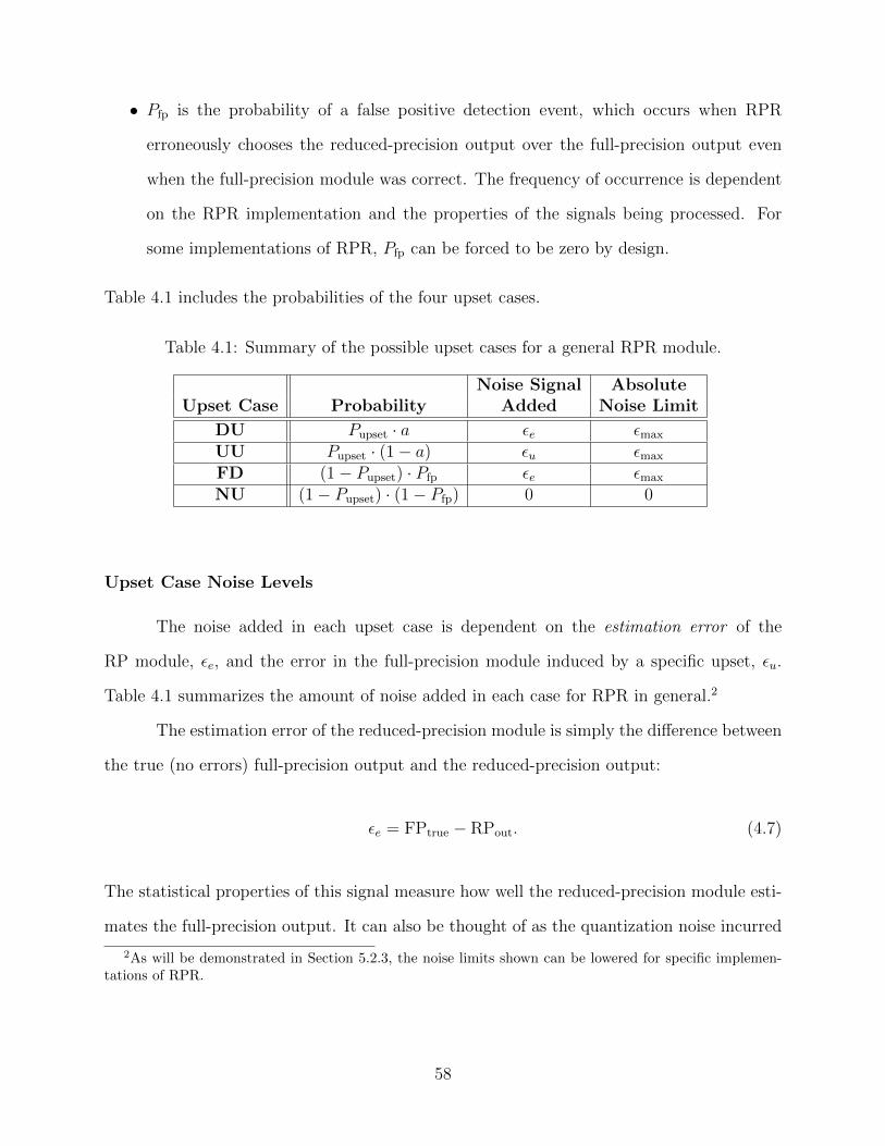
• Pfp is the probability of a false positive detection event, which occurs when RPR
erroneously chooses the reduced-precision output over the full-precision output even
when the full-precision module was correct. The frequency of occurrence is dependent
on the RPR implementation and the properties of the signals being processed. For
some implementations of RPR, Pfp can be forced to be zero by design.
Table 4.1 includes the probabilities of the four upset cases.
Table 4.1: Summary of the possible upset cases for a general RPR module.
Noise Signal AbsoluteUpset Case Probability Added Noise Limit
DU Pupset · a εe εmax
UU Pupset · (1− a) εu εmax
FD (1− Pupset) · Pfp εe εmax
NU (1− Pupset) · (1− Pfp) 0 0
Upset Case Noise Levels
The noise added in each upset case is dependent on the estimation error of the
RP module, εe, and the error in the full-precision module induced by a specific upset, εu.
Table 4.1 summarizes the amount of noise added in each case for RPR in general.2
The estimation error of the reduced-precision module is simply the difference between
the true (no errors) full-precision output and the reduced-precision output:
εe = FPtrue − RPout. (4.7)
The statistical properties of this signal measure how well the reduced-precision module esti-
mates the full-precision output. It can also be thought of as the quantization noise incurred
2As will be demonstrated in Section 5.2.3, the noise limits shown can be lowered for specific implemen-tations of RPR.
58

by using a reduced-precision operation. This signal and its statistics can sometimes be com-
puted for a specific implementation of an RPR module [4]. Appendix B includes some sample
εe data for an FIR filter design as an example of the properties of this signal.
The signal εu is the difference between the true and actual full-precision outputs:
εu = FPtrue − FPout. (4.8)
This signal is non-zero when an upset has affected the full-precision module. The statistical
properties of this signal are heavily dependent on the module implemented, the signal being
processed, and the location of the upset in the module. For some upsets, this signal is very
small compared to the desired output signal. For others, it can be very large. For this reason,
it is impossible to generalize the properties of this signal. Section B.2 in Appendix B shows
the probability mass functions (pmfs) of εu for several SEUs within an FIR filter design,
demonstrating how different these signals can be.
Although the specifics of εu cannot be generalized, the maximum magnitude of this
signal can be stated when limited to the UU upset case, which is the case in which this signal
is important, according to Table 4.1. This maximum value is the maximum undetected error
value of the RPR system, which is also the maximum magnitude of εe:
εmax = max |εe|. (4.9)
This maximum value is dependent on the type of RPR and the bit-width of the RP modules.
RPR cannot be guaranteed to detect errors smaller than this value. Since the full-precision
and reduced-precision modules may differ by this amount, RPR cannot distinguish between
such low-magnitude upsets and the natural difference between the full- and reduced-precision
outputs.
59
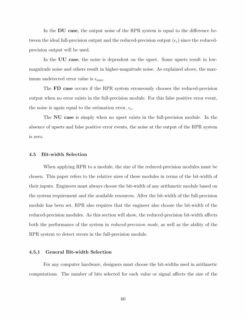
In the DU case, the output noise of the RPR system is equal to the difference be-
tween the ideal full-precision output and the reduced-precision output (εe) since the reduced-
precision output will be used.
In the UU case, the noise is dependent on the upset. Some upsets result in low-
magnitude noise and others result in higher-magnitude noise. As explained above, the max-
imum undetected error value is εmax.
The FD case occurs if the RPR system erroneously chooses the reduced-precision
output when no error exists in the full-precision module. For this false positive error event,
the noise is again equal to the estimation error, εe.
The NU case is simply when no upset exists in the full-precision module. In the
absence of upsets and false positive error events, the noise at the output of the RPR system
is zero.
4.5 Bit-width Selection
When applying RPR to a module, the size of the reduced-precision modules must be
chosen. This paper refers to the relative sizes of these modules in terms of the bit-width of
their inputs. Engineers must always choose the bit-width of any arithmetic module based on
the system requirement and the available resources. After the bit-width of the full-precision
module has been set, RPR also requires that the engineer also choose the bit-width of the
reduced-precision modules. As this section will show, the reduced-precision bit-width affects
both the performance of the system in reduced-precision mode, as well as the ability of the
RPR system to detect errors in the full-precision module.
4.5.1 General Bit-width Selection
For any computer hardware, designers must choose the bit-widths used in arithmetic
computations. The number of bits selected for each value or signal affects the size of the
60
system as well as its ability to represent numbers. Using more bits for a value gives greater
integer range and/or fractional precision but uses more hardware.
In DSP systems, where real numbers are typically represented, either fixed-point or
floating point numbers are used. FPGAs most often use fixed-point arithmetic rather than
the more flexible but more costly floating-point arithmetic [65]. Except where indicated
otherwise, the numbers represented in this dissertation are in fixed-point, Qn format: 2’s
complement numbers in the range [-1,1) with n bits to the right of the binary point and only
the sign bit to the left.
The inability of a fixed bit-width number to precisely represent a real number is called
quantization. The difference between the real number and its quantized digital value is the
quantization error. For a signal, the error signal is called the quantization noise [66]. A
DSP engineer must take this quantization noise into account when designing a system. The
optimization of bit-widths for the signals within DSP systems is an actively studied field and
will not be treated here [67]–[69].
As an example of quantization error, Figure 4.4 shows the number 0.3359375 rep-
resented with various amounts of precision in binary and decimal representations. As the
number of bits used to represent the number shrinks, the estimation becomes worse. In the
case of a fractional number truncated from n bits to k bits, the maximum error is 2−k−2−n,
which would happen if all of the bits truncated in the n-bit number were 1.
Figure 4.4: Truncation of a fixed-point binary number to several levels of precision.
61
4.5.2 RPR Bit-widths
The selection of bit-widths for the modules in an RPR system is similar to the general
bit-width selection problem. The full-precision module in an RPR system is assumed to
use the same bit-width that an engineer would select for the unmitigated module. The
reduced-precision module naturally has a smaller bit-width and uses less hardware than the
original module. This dissertation refers to the bit-widths of the full-precision and reduced-
precision modules as B and Br, respectively. The full-precision module has QB inputs and
the reduced-precision modules have QBr inputs.
The bit-width of the RP modules, Br affects two main properties: the estimation
error, εe, of the reduced-precision modules and the error detection capability, limited by
εmax, of the RPR system. The estimation error, εe, is directly determined by this bit-width.
The larger the value of Br, the smaller the estimation error and the lower the noise at the
output of the system in the DU and FD error cases. If Br = B, the expected difference
between the two is zero and the result is essentially equivalent to TMR. As Br decreases,
however, the range of this expected difference grows because the module is a less-perfect
estimator of the full-precision output. Figure 4.4 emphasizes that as a bit-width such as Br
decreases, the estimation error of the true value increases.
The error detection capability is also dependent on Br. A larger bit-width results in
a better estimate of the FP output, which means a higher confidence in the estimate and a
tighter bound on the error. Br determines the value εmax, the maximum difference between
the full-precision and reduced-precision outputs. From Table 4.1, this value bounds the error
in the UU condition since upsets any larger than this value can be detected.
In relation to the estimation error, Br also determines the performance of the system
in the DU and FD error cases, when the RPR system is in reduced-precision mode. Br can be
chosen similar to the method the engineer used for choosing B by using relaxed constraints
on the quantization noise. Although this noise is greater in reduced-precision mode, this mode
is only active when the full-precision module has a significant fault due to a soft error or in
62

the case of a false detection event. Depending on the SEU rate the system operates in and
the false positive probability, operation in this mode may be quite infrequent. With a low
probability of occurrence, lower performance may be tolerated from the reduced-precision
module by using a smaller Br value, resulting in a savings in circuit area. Section 6.2 will
explore the methods for choosing Br in more detail for one variation of RPR.
4.6 RPR Decision Blocks
In addition to the reduced-precision blocks which must be designed and for which
Br must be chosen, the RPR decision block must also be created. The RPR decision block
uses the outputs of the three RPR modules to determine whether to use the full-precision
or reduced-precision output. In essence, RPR can be thought of as an encoding scheme in
which the reduced-precision outputs are the redundant portion of the codeword. The RPR
decision block is the decoding circuit used to map the redundant word back to a single, valid
code word.
The design of the decision block is dependent upon the variation of RPR used. Chap-
ter 5 will describe the decision blocks used for each type of RPR and how their design affects
the cost and performance of the RPR implementation.
4.7 RPR Demonstration
As a demonstration of the RPR technique, this section will provide the results of fault
injection experiments on several FPGA designs. To evaluate RPR’s potential for protecting
communications applications, we applied RPR to the feed-forward binary PAM matched filter
detector of Section 3.5. This demonstration applies the RPR technique to three different
receiver configurations, varying the matched filter architecture and the coefficient values.
These initial experiments with RPR confirm that RPR is able to provide good pro-
tection against the most critical SEUs in these communications systems at a much lower cost
than TMR. The experiments also show that RPR’s effectiveness is not strongly dependent on
63
either of these filter parameters, while it can be a cost-effective alternative to TMR. Future
chapters will look further into the implementation details of RPR, such as how to select the
best Br value and what specific implementation of RPR is best.
4.7.1 Experimental Configuration
In order to test the effectiveness of RPR on a communications system, we applied the
technique to several of the designs described in Section 3.5:
• “16b logic α = 1.0” means the SRRC pulse shape with α = 1.0 using 16-bit inputs and
filter coefficients.
• “16b logic α = 0.25” means the SRRC pulse shape with α = 0.25 using 16-bit inputs
and filter coefficients.
• “16b dsp48 α = 1.0” means the SRRC pulse shape with α = 1.0 using 16-bit inputs
and filter coefficients and using the embedded DSP blocks of the Virtex 4 SX55 FPGA.
The fault injection experiments run were of the same form as those in Section 3.4
except that the utilized configuration bits were discovered rather than the sensitive bits.
This allowed the full designs to be tested, even when redundancy would typically mask some
errors. Section A.2 in Appendix A describes this distinction in detail.
To determine the effectiveness of RPR, we measured the effect on the BER of every
possible SEU in each of these systems. To measure the efficiency of RPR, we used TMR to
protect the same circuits and compared the results in terms of circuit area consumed. By
using RPR, we expected to eliminate or significantly reduce “catastrophic” SEUs compared
to the original designs. We also expected to see a significantly smaller implementation cost
(in terms of circuit area overhead) than TMR.
64
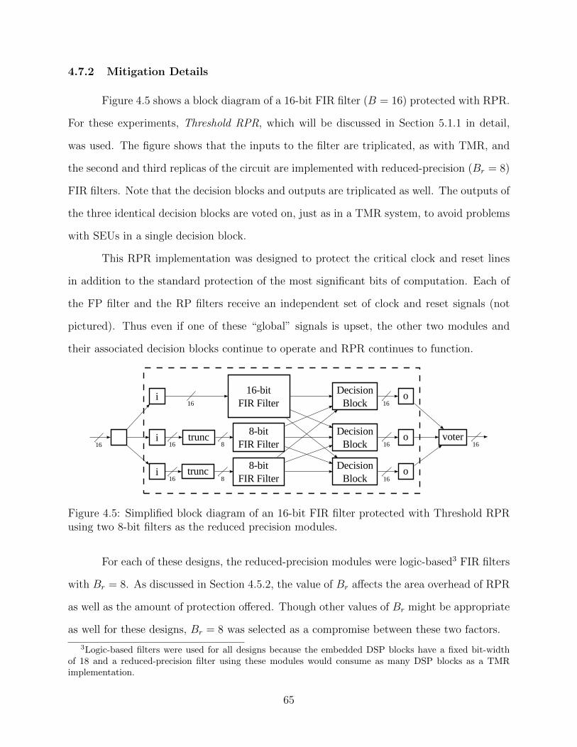
4.7.2 Mitigation Details
Figure 4.5 shows a block diagram of a 16-bit FIR filter (B = 16) protected with RPR.
For these experiments, Threshold RPR, which will be discussed in Section 5.1.1 in detail,
was used. The figure shows that the inputs to the filter are triplicated, as with TMR, and
the second and third replicas of the circuit are implemented with reduced-precision (Br = 8)
FIR filters. Note that the decision blocks and outputs are triplicated as well. The outputs of
the three identical decision blocks are voted on, just as in a TMR system, to avoid problems
with SEUs in a single decision block.
This RPR implementation was designed to protect the critical clock and reset lines
in addition to the standard protection of the most significant bits of computation. Each of
the FP filter and the RP filters receive an independent set of clock and reset signals (not
pictured). Thus even if one of these “global” signals is upset, the other two modules and
their associated decision blocks continue to operate and RPR continues to function.
Figure 4.5: Simplified block diagram of an 16-bit FIR filter protected with Threshold RPRusing two 8-bit filters as the reduced precision modules.
For each of these designs, the reduced-precision modules were logic-based3 FIR filters
with Br = 8. As discussed in Section 4.5.2, the value of Br affects the area overhead of RPR
as well as the amount of protection offered. Though other values of Br might be appropriate
as well for these designs, Br = 8 was selected as a compromise between these two factors.
3Logic-based filters were used for all designs because the embedded DSP blocks have a fixed bit-widthof 18 and a reduced-precision filter using these modules would consume as many DSP blocks as a TMRimplementation.
65
A value of Th = 0.5 was chosen as the threshold to compare between the reduced-
precision and full-precision outputs. For these filter sizes, this threshold ensured that an
error would never be declared when no SEUs were present in the system. Sections 5.1.1
and 6.1 will discuss the selection of the value of Th in more detail.
In these experiments, the triplicated RPR decision blocks were imperfect and were
found to be susceptible to several single SEU-induced errors. Although the RPR decision
block was triplicated in each case (essentially, TMR was applied to that module), some
SEUs caused upsets more than one of the replicas and overcame the TMR protection. This
is reflected in the test results, where some of the catastrophic SEUs remain in the RPR
implementation. TMR has been shown to be imperfect in FPGAs in some instances, where
a single configuration bit affects signal routing in two of the three TMR domains [70]. This
problem has also been shown to be correctable, in a large extent, using reliability-oriented
routing techniques [71]. Section D.3 (in Appendix D) discusses this issue in more detail.
4.7.3 Experimental Results
Tables 4.2 and 4.3 show the numerical results from the fault injection experiments.
The tables illustrate the sensitivity differences between the RPR and TMR implementations
of each filter design and their sensitivity improvements over the original unmitigated filter.
Table 4.2 reports on the number of SEUs observed in each of the four classes defined
in Section 3.5.2. The implementation overhead of each mitigation technique in terms of
FPGA slices is given as well as the reduction in the number of catastrophic (Class 3 and 4)
SEUs. This table also shows the factor by which the failure rate of each system (in terms of
catastrophic upsets) improved.
This table shows that virtually all of the SEUs affecting the three TMR designs fall
in the Class 1 category (no measurable SNR loss). In fact, there were only two upsets that
adversely affected the output of the TMR design. This confirms the effectiveness of the
TMR approach in eliminating virtually all SEU-induced errors. The number of FPGA slices
66
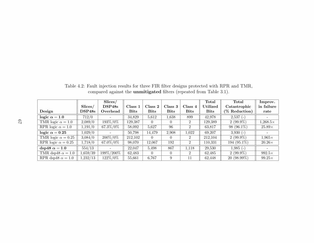
Table 4.2: Fault injection results for three FIR filter designs protected with RPR and TMR,compared against the unmitigated filters (repeated from Table 3.1).
Slices/ Total Total Improv.Slices/ DSP48s Class 1 Class 2 Class 3 Class 4 Utilized Catastrophic in failure
Design DSP48s Overhead Bits Bits Bits Bits Bits (% Reduction) rate
logic α = 1.0 712/0 - 34,829 5,612 1,638 899 42,978 2,537 (-) -TMR logic α = 1.0 2,089/0 193%/0% 129,387 0 0 2 129,389 2 (99.9%) 1,268.5×RPR logic α = 1.0 1,191/0 67.3%/0% 58,092 5,627 96 2 63,817 98 (96.1%) 25.89×logic α = 0.25 1,029/0 - 50,798 14,479 2,908 1,022 69,207 3,930 (-) -TMR logic α = 0.25 3,084/0 200%/0% 212,102 0 0 2 212,104 2 (99.9%) 1,965×RPR logic α = 0.25 1,718/0 67.0%/0% 98,070 12,067 192 2 110,331 194 (95.1%) 20.26×dsp48 α = 1.0 554/13 - 22,047 5,498 867 1,118 29,530 1,985 (-) -TMR dsp48 α = 1.0 1,659/39 199%/200% 62,483 0 0 2 62,485 2 (99.9%) 992.5×RPR dsp48 α = 1.0 1,232/13 122%/0% 55,661 6,767 9 11 62,448 20 (98.99%) 99.25×
67

and the total number of utilized bits in each TMR design, of course, increased due to the
logic added by the filter replicas. The addition of these SEUs is reflected in the increase in
the number of Class 1 SEUs as compared to the original design. Also notice that the failure
rate improvement factor for each TMR design is very high. Theoretically, TMR eliminates
all SEUs and offers an infinite improvement in failure rate. Similar to the triplicated RPR
decision blocks, however, some catastrophic SEUs remain in these TMR implementations,
resulting in a finite failure rate improvement.
The RPR designs also showed good resilience to SEUs. For example, for the 16-bit
logic-based filter with α = 1.0, the 899 Class 4 SEUs were reduced to 2 and the number of
Class 3 SEUs was reduced from 1,638 to 96. In fact, RPR reduced the number of catastrophic
SEUs by over 95% for each design, improving the failure rate of each by over 20×. Similar
to TMR, the added redundant modules increased the total number of SEUs affecting the
design as well as the number of Class 1 errors. In two of the RPR designs, there was also an
increase in the number of Class 2 SEUs. As discussed earlier, however, these SEUs are not
as critical since the errors induced by these SEUs are likely to be correctable by standard
communications error-handling techniques such as error-control coding.
Table 4.3 shows the SNR loss results for the RPR and TMR filter designs. For this
table, we present a normalized percentage figure by dividing the number of SEUs in each
category by the number of utilized configuration bits in the original unmitigated design to
obtain each percentage. Note again that the TMR designs show no SNR loss for virtually
all SEUs. Again, taking the 16-bit logic-based filter with α = 1.0 as an example, we see
that RPR technique reduced the percentage of SEUs that caused large SNR losses. Losses
of more than 6 dB were reduced from 9.21% to 1.19% while losses of more than 3 dB were
reduced from 11.20% to 4.17%.
Figures 4.6 – 4.8 show BER plots which illustrate the impact of all SEUs on each
of the three RPR designs. As with the unmitigated versions of the designs reported on in
Section 3.5.2, the vast majority of SEUs cause little impact on the BER curve. Compare
68
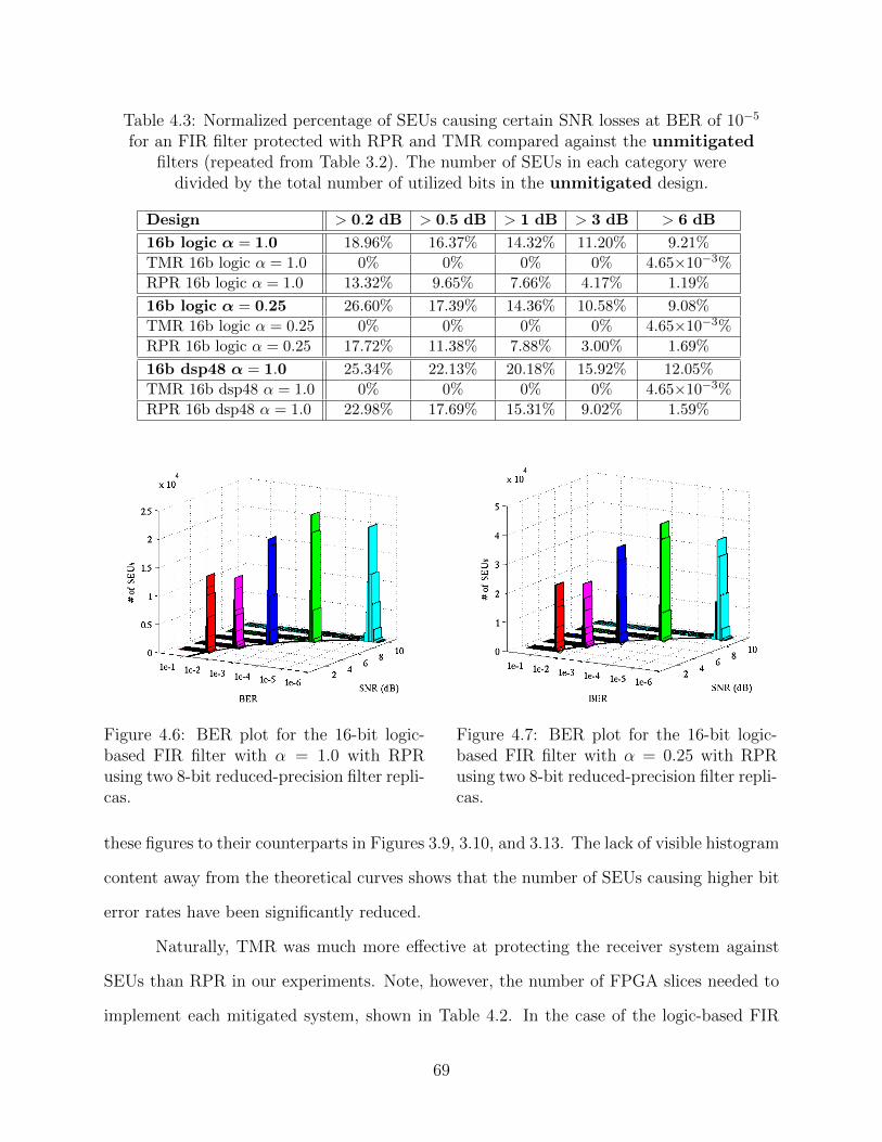
Table 4.3: Normalized percentage of SEUs causing certain SNR losses at BER of 10−5
for an FIR filter protected with RPR and TMR compared against the unmitigatedfilters (repeated from Table 3.2). The number of SEUs in each category were
divided by the total number of utilized bits in the unmitigated design.
Design > 0.2 dB > 0.5 dB > 1 dB > 3 dB > 6 dB
16b logic α = 1.0 18.96% 16.37% 14.32% 11.20% 9.21%
TMR 16b logic α = 1.0 0% 0% 0% 0% 4.65×10⁻³%
RPR 16b logic α = 1.0 13.32% 9.65% 7.66% 4.17% 1.19%
16b logic α = 0.25 26.60% 17.39% 14.36% 10.58% 9.08%
TMR 16b logic α = 0.25 0% 0% 0% 0% 4.65×10⁻³%
RPR 16b logic α = 0.25 17.72% 11.38% 7.88% 3.00% 1.69%
16b dsp48 α = 1.0 25.34% 22.13% 20.18% 15.92% 12.05%
TMR 16b dsp48 α = 1.0 0% 0% 0% 0% 4.65×10⁻³%
RPR 16b dsp48 α = 1.0 22.98% 17.69% 15.31% 9.02% 1.59%
Figure 4.6: BER plot for the 16-bit logic-based FIR filter with α = 1.0 with RPRusing two 8-bit reduced-precision filter repli-cas.
Figure 4.7: BER plot for the 16-bit logic-based FIR filter with α = 0.25 with RPRusing two 8-bit reduced-precision filter repli-cas.
these figures to their counterparts in Figures 3.9, 3.10, and 3.13. The lack of visible histogram
content away from the theoretical curves shows that the number of SEUs causing higher bit
error rates have been significantly reduced.
Naturally, TMR was much more effective at protecting the receiver system against
SEUs than RPR in our experiments. Note, however, the number of FPGA slices needed to
implement each mitigated system, shown in Table 4.2. In the case of the logic-based FIR
69
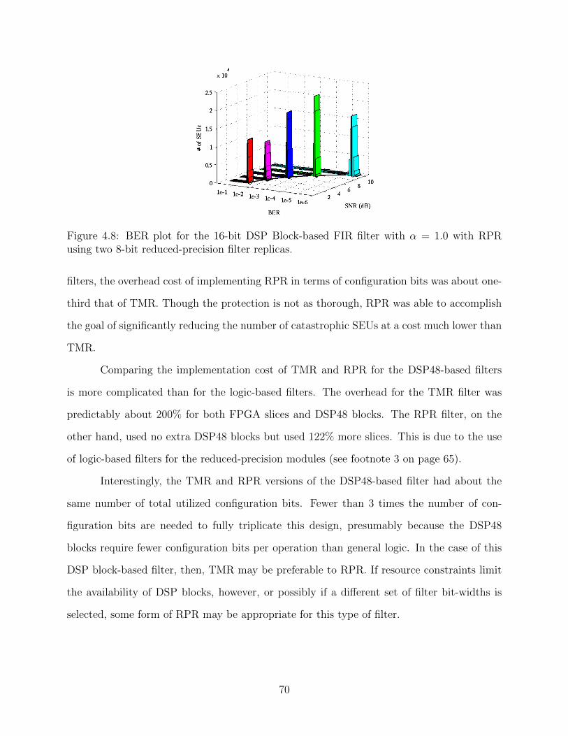
Figure 4.8: BER plot for the 16-bit DSP Block-based FIR filter with α = 1.0 with RPRusing two 8-bit reduced-precision filter replicas.
filters, the overhead cost of implementing RPR in terms of configuration bits was about one-
third that of TMR. Though the protection is not as thorough, RPR was able to accomplish
the goal of significantly reducing the number of catastrophic SEUs at a cost much lower than
TMR.
Comparing the implementation cost of TMR and RPR for the DSP48-based filters
is more complicated than for the logic-based filters. The overhead for the TMR filter was
predictably about 200% for both FPGA slices and DSP48 blocks. The RPR filter, on the
other hand, used no extra DSP48 blocks but used 122% more slices. This is due to the use
of logic-based filters for the reduced-precision modules (see footnote 3 on page 65).
Interestingly, the TMR and RPR versions of the DSP48-based filter had about the
same number of total utilized configuration bits. Fewer than 3 times the number of con-
figuration bits are needed to fully triplicate this design, presumably because the DSP48
blocks require fewer configuration bits per operation than general logic. In the case of this
DSP block-based filter, then, TMR may be preferable to RPR. If resource constraints limit
the availability of DSP blocks, however, or possibly if a different set of filter bit-widths is
selected, some form of RPR may be appropriate for this type of filter.
70
4.8 Summary
This chapter gave an introduction to the RPR technique for FPGA systems. It
presented the general architecture of RPR and explained the different operating modes of
RPR. Fault injection experiments demonstrated that RPR is an efficient means to protect
an FPGA-based communications system from catastrophic SEUs. Combined with the fact
that most non-catastrophic SEUs result in effects similar to additive noise, RPR can be a
good alternative to TMR for low-cost SEU mitigation.
These experiments are only an initial demonstration of RPR. Future chapters will look
into RPR in more detail and show how the results shown here can be improved. Chapter 5
will describe and contrast three different variations of RPR and select the best type for use
in FPGA systems. Chapter 6 focuses on one version of RPR and shows how to calculate the
best Br value and other parameters as well as how to integrate RPR into larger systems.
These chapters will also present fault injection results to demonstrate improvements over
these initial results.
71

72
CHAPTER 5. COMPARISON OF RPR VARIATIONS
As suggested in the previous chapter, there are many ways to implement RPR. This
chapter describes and analyzes three different variations of RPR. Each variation includes a
full-precision module as well as two reduced-precision modules and each has a method of
choosing between the different outputs. We give these three variations of RPR the names
Threshold RPR, Bounded RPR, and Reduced-Precision TMR (RP-TMR), in order to dis-
tinguish between them. Threshold RPR and Bounded RPR were suggested by previous
researchers while RP-TMR is a novel variation of RPR introduced in this dissertation. This
chapter will describe the three methods in detail and will explain the relative costs and
benefits of each.
Section 5.1 describes the architecture and function of each variation of RPR. Sec-
tion 5.2 compares the potential cost and performance of each variation of RPR on FPGA
systems. As a practical demonstration of these variations, Section 5.3 presents fault injec-
tion experiments on a simple communication system protected with each type of RPR and
compares the results.
5.1 RPR Variations
Each variation of RPR has a distinct architecture and error handling method. Before
describing each variation of RPR in detail, a brief summary of each is appropriate:
Threshold RPR uses two identical reduced-precision modules to estimate the full-
precision result and determine if the full-precision module is in error. It was suggested
by Shim, et al. as a protection against voltage over-scaling (VOS) for ASICs [4]. It was
73

also suggested as a possible protection against soft errors in ASICs [72]. In contrast, this
dissertation evaluates this type of RPR specifically for FPGAs and communications systems.
Bounded RPR uses distinct reduced-precision modules whose outputs bound the full-
precision module in the absence of errors. The two reduced-precision modules form two less
precise bounds on the desired full-precision result. Bounded RPR was designed by Snodgrass
specifically for FPGA-based systems [5].
RP-TMR uses gate-level TMR on the upper-most bits of computation to directly
protect the most significant bits of the module output. This novel variation of RPR could also
be considered a variation of TMR. Section 3.7 suggested that TMR could possibly be applied
to the most critical sections of the circuit directly in order to reduce the cost of full TMR
while retaining the most significant benefits. RP-TMR uses this straightforward approach
and will be considered against the first two RPR techniques which were first presented
elsewhere.
The following three sections describe the function and implementation of these three
variations of RPR. The general architecture of each is given, including the structure and
function of the decision block. In addition, the design of the reduced-precision modules is
discussed for each variation.
5.1.1 Threshold RPR
This section analyzes the type of RPR introduced by Shim, et al. [54]. It is called
“Threshold RPR” due to the use of a pre-set threshold to determine when the full-precision
module is in error.
Overview
Threshold RPR is implemented by creating two identical reduced-precision (RP)
versions of the module to be protected, as illustrated in Figure 5.1. The outputs of the two
RP modules are used to determine if there is a fault in the full-precision (FP) module. If the
74
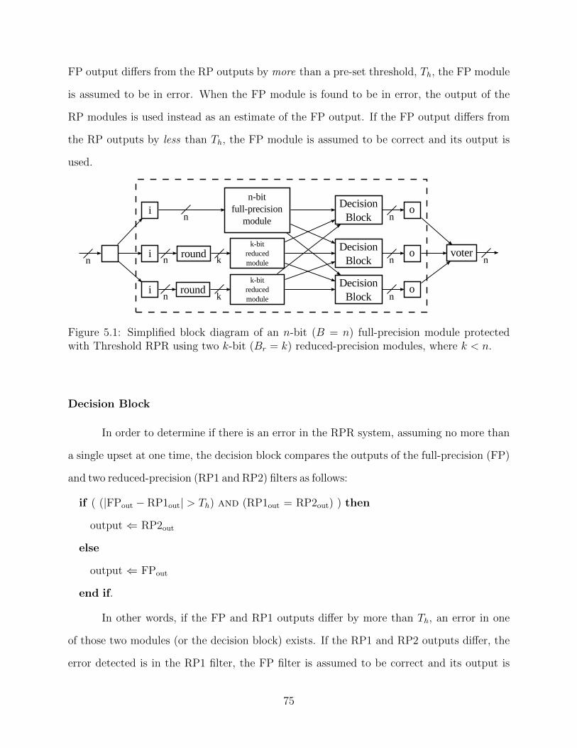
FP output differs from the RP outputs by more than a pre-set threshold, Th, the FP module
is assumed to be in error. When the FP module is found to be in error, the output of the
RP modules is used instead as an estimate of the FP output. If the FP output differs from
the RP outputs by less than Th, the FP module is assumed to be correct and its output is
used.
Figure 5.1: Simplified block diagram of an n-bit (B = n) full-precision module protectedwith Threshold RPR using two k-bit (Br = k) reduced-precision modules, where k < n.
Decision Block
In order to determine if there is an error in the RPR system, assuming no more than
a single upset at one time, the decision block compares the outputs of the full-precision (FP)
and two reduced-precision (RP1 and RP2) filters as follows:
if ( (|FPout − RP1out| > Th) and (RP1out = RP2out) ) then
output ⇐ RP2out
else
output ⇐ FPout
end if.
In other words, if the FP and RP1 outputs differ by more than Th, an error in one
of those two modules (or the decision block) exists. If the RP1 and RP2 outputs differ, the
error detected is in the RP1 filter, the FP filter is assumed to be correct and its output is
75

used. If the threshold is exceeded and the RP1 and RP2 outputs are equal, the FP module
is assumed to be in error and the output of the RP2 filter is used (though either RP output
would be suitable). Thus the full-precision output is used when no error is found or when the
two reduced-precision modules disagree. Otherwise, the reduced-precision output is used,
providing an estimate of the correct full-precision output.
A block diagram of this decision block is shown in Figure 5.2 and its place in the
overall Threshold RPR system is seen in Figure 5.1. Note in Figure 5.1 that the RPR
decision block can be triplicated since these modules are just as susceptible to SEUs as the
computation modules. As with TMR, the three outputs are combined with an SEU-immune
voter off chip.
Figure 5.2: Block diagram of a Threshold RPR decision block.
Shim suggested that the Threshold RPR decision block can be optimized to consume
less area if the value of Th is constrained to a power of two. This modified decision block
is shown in Figure 5.3. The module takes the difference of the full-precision and reduced-
precision module outputs, and uses simple m-bit NAND and OR gates on the upper bits
of this difference to determine if the threshold is exceeded. The width m of the simplified
comparator gates is dependent on the threshold value chosen. This circuit replaces the three
upper modules in Figure 5.2.
The lower cost of this optimized decision block can make Threshold RPR more ef-
ficient, requiring less overhead. Due to the restriction of Th to a power of two, however,
76

this type of decision block is limited in the precision offered by the threshold value. This
can limit the effectiveness of the decision block in situations when a more precise value is
preferable.
Figure 5.3: Block diagram of a optimization on the Threshold RPR decision block suggestedby Shim [4].
For either type of decision block, the value of Th affects the balance between the DU
and the UU upset cases (as defined in Section 4.4). Th controls the a factor in Table 4.1,
the fraction of upsets in the full-precision module with RPR detects. A smaller Th detects
lower-magnitude errors to be detected, increasing the a factor. A larger Th decreases the a
factor and allows higher-magnitude errors in the UU upset case.1
For a particular instantiation of Threshold RPR (i.e. for a particular module and Br
value), there is an optimal range for Th. If Th is too large, the full-precision output will be
used even when there are significant errors in that module. A Th that is too small will cause
the RP output to be chosen even when there are no errors in the FP module, resulting in
the false detection (FD) upset case. The limits on the optimal range of Th will be discussed
in Sections 5.2 and 6.1.
Reduced-Precision Module Design
In addition to the decision block, the reduced-precision modules must also be de-
signed. For Threshold RPR, the two reduced-precision modules are identical, making any
error in one of the modules trivial to detect. If the reduced-precision outputs differ, an upset
1Table 6.5 in Section 6.1.4 reports on some measured values of the a factor for changing Th values.
77

certainly exists in one of them and the full-precision output is used. Thus no upset in the
reduced-precision modules cause any error in the RPR system output.
Aside from having identical outputs, the reduced-precision modules may be designed
in any way and their architecture need not match that of the full-precision module. For
simplicity, this dissertation uses the same technique used to design the full-precision module
in order to design the reduced-precision module, but with reduced-precision inputs. For
example, if the full-precision module is a standard array multiplier with two (B + 1)-bit
inputs and a (B + 1)-bit output, the reduced-precision module is also designed as an array
multiplier with two (Br + 1)-bit inputs with a (Br + 1)-bit output.
5.1.2 Bounded RPR
Snodgrass introduced another type of RPR specifically for soft-error environments [5].
It is called “Bounded RPR” here because it uses two reduced-precision modules to create
bounds on the full-precision output.
Overview
Bounded RPR is similar to Threshold RPR in that two reduced-precision modules
are utilized. In this case, however, the two RP modules are not identical. Instead, the RP
modules are designed to create bounds on the FP output, as illustrated in Figure 5.4. The
output of the first RP module, RPupper, is the upper bound. The output of RPlower is the
lower bound. RPupper must be designed such that its output is always greater than or equal
to the FP module’s output for any set of inputs in the absence of SEUs. Similarly, the output
of RPlower must always be less than or equal to the FP output.
Decision Block
The function of the Bounded RPR decision block is somewhat more complex than
that of Threshold RPR. The final output is determined by comparing the relative positions
78

Figure 5.4: Simplified block diagram of a full-precision module protected with Bounded RPRusing upper-bound and lower-bound reduced precision modules.
of each of the outputs. There are several possible error cases to consider. These error cases
are illustrated in Figure 5.5 and are categorized into rows according to the module in which
the error has occurred.
Figure 5.5: Error cases for Bounded RPR, modified from [5]. Categorized in rows by thelocation of the error and in columns by the response to each type of event.
79
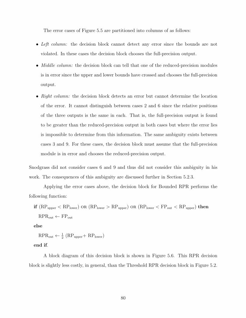
The error cases of Figure 5.5 are partitioned into columns of as follows:
• Left column: the decision block cannot detect any error since the bounds are not
violated. In these cases the decision block chooses the full-precision output.
• Middle column: the decision block can tell that one of the reduced-precision modules
is in error since the upper and lower bounds have crossed and chooses the full-precision
output.
• Right column: the decision block detects an error but cannot determine the location
of the error. It cannot distinguish between cases 2 and 6 since the relative positions
of the three outputs is the same in each. That is, the full-precision output is found
to be greater than the reduced-precision output in both cases but where the error lies
is impossible to determine from this information. The same ambiguity exists between
cases 3 and 9. For these cases, the decision block must assume that the full-precision
module is in error and chooses the reduced-precision output.
Snodgrass did not consider cases 6 and 9 and thus did not consider this ambiguity in his
work. The consequences of this ambiguity are discussed further in Section 5.2.3.
Applying the error cases above, the decision block for Bounded RPR performs the
following function:
if (RPupper < RPlower) or (RPlower > RPupper) or (RPlower < FPout < RPupper) then
RPRout ← FPout
else
RPRout ← 12
(RPupper+ RPlower)
end if.
A block diagram of this decision block is shown in Figure 5.6. This RPR decision
block is slightly less costly, in general, than the Threshold RPR decision block in Figure 5.2.
80

Figure 5.6: Block diagram of a Bounded RPR decision block. Sign extensions, where neces-sary, are not shown in this diagram.
Reduced-Precision Module Design
Designing the reduced-precision blocks for Bounded RPR is also more complex than
Threshold RPR. As discussed above, Bounded RPR requires that the outputs of the upper
and lower reduced-precision modules bound the full-precision output for all possible inputs
and input sequences. For simple modules this can be done by rounding up the input to the
upper bound module and rounding down the input to the lower bound module. However, this
works only for the most simplistic functions and, as discussed by Snodgrass [5], could require
the addition of complex hardware to ensure the correct bounds even for simple functions.
Sullivan was able to design bounding modules for several arithmetic modules by making
some simplifying assumptions [64].
Alternately, the RP modules can be designed in the same manner as Threshold RPR
and then adding or subtracting the maximum estimation error, εmax, as in Figure 5.7. This
would essentially re-create Threshold RPR, but requires an extra adder for each RP module.
Snodgrass also suggests that a reduced-precision computation module could be im-
plemented as a lookup table. If this lookup table can be pre-generated, the output of the two
RP modules can be made to ensure correct bounding of the FP output. In fact, they can be
81
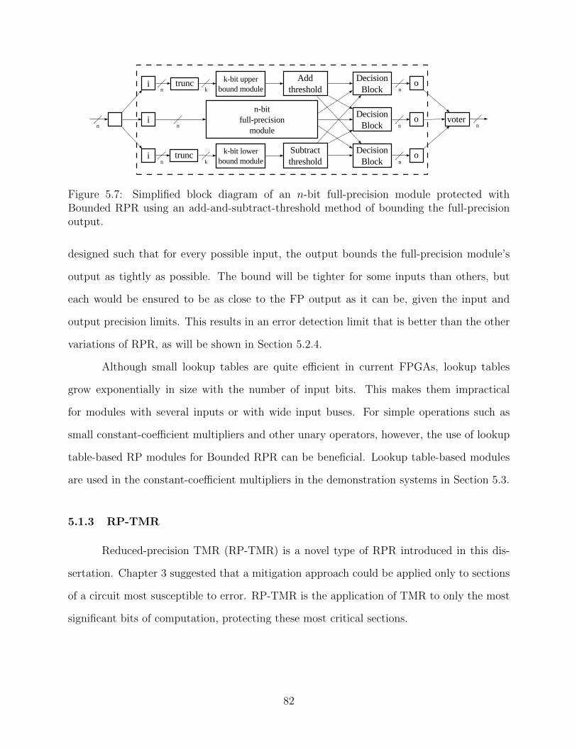
Figure 5.7: Simplified block diagram of an n-bit full-precision module protected withBounded RPR using an add-and-subtract-threshold method of bounding the full-precisionoutput.
designed such that for every possible input, the output bounds the full-precision module’s
output as tightly as possible. The bound will be tighter for some inputs than others, but
each would be ensured to be as close to the FP output as it can be, given the input and
output precision limits. This results in an error detection limit that is better than the other
variations of RPR, as will be shown in Section 5.2.4.
Although small lookup tables are quite efficient in current FPGAs, lookup tables
grow exponentially in size with the number of input bits. This makes them impractical
for modules with several inputs or with wide input buses. For simple operations such as
small constant-coefficient multipliers and other unary operators, however, the use of lookup
table-based RP modules for Bounded RPR can be beneficial. Lookup table-based modules
are used in the constant-coefficient multipliers in the demonstration systems in Section 5.3.
5.1.3 RP-TMR
Reduced-precision TMR (RP-TMR) is a novel type of RPR introduced in this dis-
sertation. Chapter 3 suggested that a mitigation approach could be applied only to sections
of a circuit most susceptible to error. RP-TMR is the application of TMR to only the most
significant bits of computation, protecting these most critical sections.
82
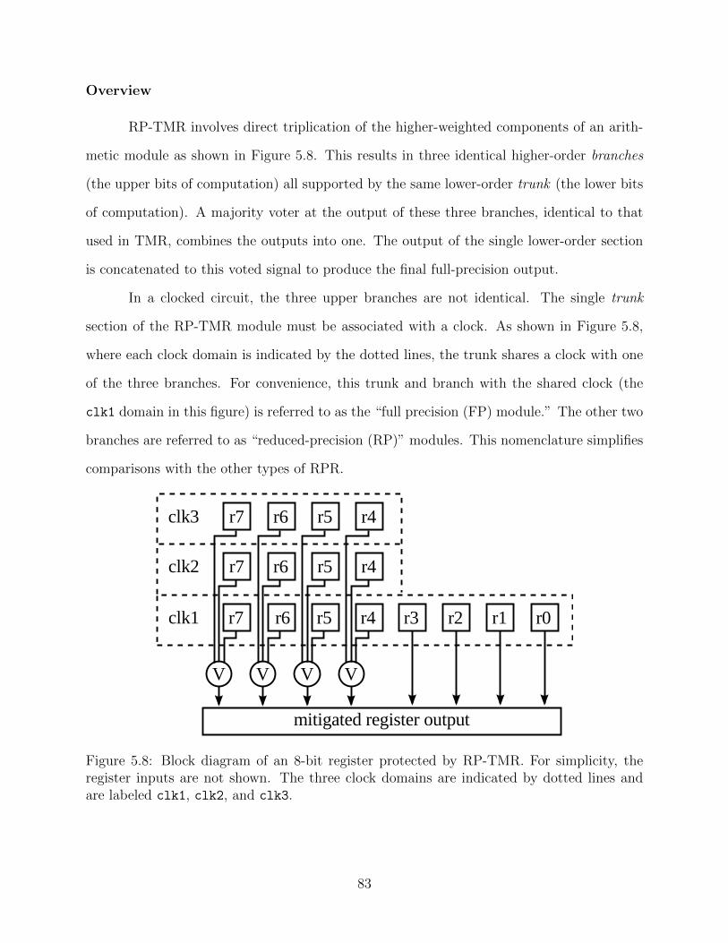
Overview
RP-TMR involves direct triplication of the higher-weighted components of an arith-
metic module as shown in Figure 5.8. This results in three identical higher-order branches
(the upper bits of computation) all supported by the same lower-order trunk (the lower bits
of computation). A majority voter at the output of these three branches, identical to that
used in TMR, combines the outputs into one. The output of the single lower-order section
is concatenated to this voted signal to produce the final full-precision output.
In a clocked circuit, the three upper branches are not identical. The single trunk
section of the RP-TMR module must be associated with a clock. As shown in Figure 5.8,
where each clock domain is indicated by the dotted lines, the trunk shares a clock with one
of the three branches. For convenience, this trunk and branch with the shared clock (the
clk1 domain in this figure) is referred to as the “full precision (FP) module.” The other two
branches are referred to as “reduced-precision (RP)” modules. This nomenclature simplifies
comparisons with the other types of RPR.
Figure 5.8: Block diagram of an 8-bit register protected by RP-TMR. For simplicity, theregister inputs are not shown. The three clock domains are indicated by dotted lines andare labeled clk1, clk2, and clk3.
83

As examples of RP-TMR implementation, Figures 5.9 and 5.10 illustrate an RP-
TMR adder and multiplier, respectively. Figure 5.9 shows the entire redundant adder circuit.
Figure 5.10 shows a standard array multiplier with fractional inputs and marks the portion of
the circuit that is triplicated for RP-TMR. Note that the redundant portion of the RP-TMR
multiplier makes up a reduced-precision multiplier similar to a standalone reduced-precision
module.
Figure 5.9: Block diagram of an 8-bit adder protected by RP-TMR. For simplicity, the xand y inputs of each full adder are not shown. The three clock domains, corresponding tothe clock domains of the inputs to each full adder sub-module, are indicated by dotted linesand are labeled clk1, clk2, and clk3. The full adder submodule is detailed in the inset.
For each module, the branches and trunk work together to produce the full-precision
output. The three higher-order branches of each RP-TMR module are essentially stand-alone
reduced-precision modules. Alone, each branch produces an estimate of the full-precision
output. In the case of the adder or multiplier, the output of the lower-order trunk feeds into
all three branches. When the lower-order trunk produces a useful output, these branches are
able to give a better estimate of the true full-precision result.
The output of the upper branches depends on the location of any upsets within the
RP-TMR module. When the entire circuit is free of upsets, the branches all produce the
84
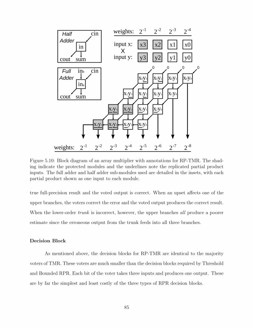
Figure 5.10: Block diagram of an array multiplier with annotations for RP-TMR. The shad-ing indicate the protected modules and the underlines note the replicated partial productinputs. The full adder and half adder sub-modules used are detailed in the insets, with eachpartial product shown as one input to each module.
true full-precision result and the voted output is correct. When an upset affects one of the
upper branches, the voters correct the error and the voted output produces the correct result.
When the lower-order trunk is incorrect, however, the upper branches all produce a poorer
estimate since the erroneous output from the trunk feeds into all three branches.
Decision Block
As mentioned above, the decision blocks for RP-TMR are identical to the majority
voters of TMR. These voters are much smaller than the decision blocks required by Threshold
and Bounded RPR. Each bit of the voter takes three inputs and produces one output. These
are by far the simplest and least costly of the three types of RPR decision blocks.
85

Reduced-Precision Module Design
RP-TMR does not have separate reduced-precision modules as Threshold RPR and
Bounded RPR do. Redundancy is added by directly triplicating the most significant bits of
computation of the unmitigated module. Thus the architecture of the redundant portions of
the circuit (the “reduced-precision modules”) mirrors that of the unmitigated module. This
makes the design of the redundant portions of the circuit simple, but inflexible.
5.2 RPR Variation Comparison
This section compares the cost and performance of the three variations of RPR.
Section 5.2.1 compares the area cost of the various RPR decision blocks. Section 5.2.2
compares the implementation issues for the reduced-precision modules of each type of RPR.
Section 5.2.3 compares the differences in how the four RPR upset cases manifest themselves
for each RPR variation. Section 5.2.4 compares the error detection limits for each type of
RPR. Section 5.2.5 discusses some issues related to the FPGA implementation of the RPR
variations.
5.2.1 Decision Block Cost
The three variations of RPR have distinct overhead costs. The cost of the reduced-
precision modules can be similar across all three variations, depending on how they are
designed. The cost of the RPR decision blocks, however, can vary greatly. Appendix D
estimates the cost of the RPR decision blocks for each variation of RPR. Figure 5.11 plots
the results of these estimations in terms of the number of 4-input LUTs required for each
decision block with a range of reduced-precision bit-widths, Br.
Clearly, RP-TMR has the lowest cost of the three variations. The Bounded RPR
decision blocks have slightly lower cost than the standard Threshold RPR blocks. The
optimized Threshold RPR decision blocks are more efficient than either of these, though
these blocks have limited application, as explained in Section 5.1.1.
86
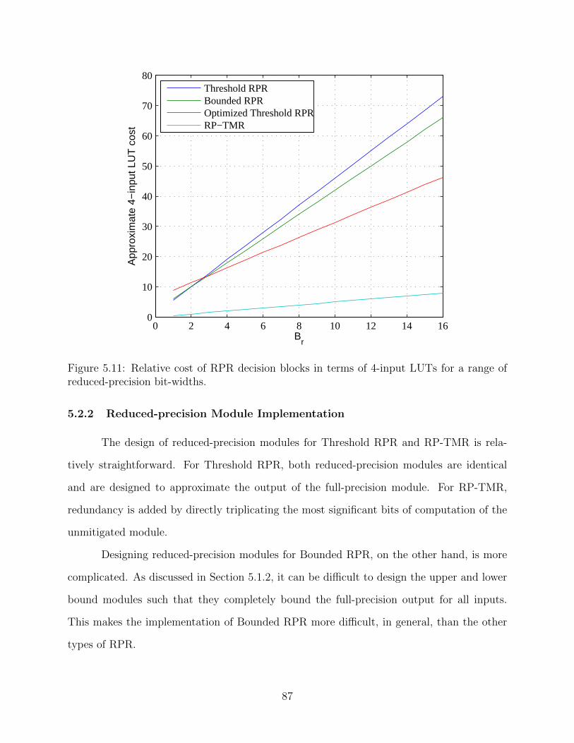
0 2 4 6 8 10 12 14 160
10
20
30
40
50
60
70
80
Br
App
roxi
mat
e 4−
inpu
t LU
T c
ost
Threshold RPRBounded RPROptimized Threshold RPRRP−TMR
Figure 5.11: Relative cost of RPR decision blocks in terms of 4-input LUTs for a range ofreduced-precision bit-widths.
5.2.2 Reduced-precision Module Implementation
The design of reduced-precision modules for Threshold RPR and RP-TMR is rela-
tively straightforward. For Threshold RPR, both reduced-precision modules are identical
and are designed to approximate the output of the full-precision module. For RP-TMR,
redundancy is added by directly triplicating the most significant bits of computation of the
unmitigated module.
Designing reduced-precision modules for Bounded RPR, on the other hand, is more
complicated. As discussed in Section 5.1.2, it can be difficult to design the upper and lower
bound modules such that they completely bound the full-precision output for all inputs.
This makes the implementation of Bounded RPR more difficult, in general, than the other
types of RPR.
87

For Threshold and Bounded RPR, there is no limitation the architecture of the
reduced-precision modules. The reduced-precision modules are designed separately from the
full-precision module. They can be created with a standard module with reduced-precision
inputs, implemented with lookup tables, or using any number of circuit optimization tech-
niques. The smaller bit-widths may result in relaxed constraints (such as timing) compared
to the full-precision module. For example, Shim suggested that reduced-precision constant-
coefficient multipliers could be replaced with shift and add operations to reduce the hardware
cost of the reduced-precision modules [72].
The redundancy added to RP-TMR, on the other hand, follows the architecture of
the unmitigated module, even if a more optimized reduced-precision module could be de-
signed. Although this strict method of creating the RP-TMR redundancy limits optimiza-
tion, it likely makes the application of RP-TMR easier to automate than either Threshold
or Bounded RPR. It should be possible to create an automated tool which could identify
the most significant bits of computation in each module within a system, assuming the ar-
chitecture of the components is known. The identified components could then be passed to
a tool such as the BYU-LANL TMR (BL-TMR) tool which can apply TMR to only those
components [73], [74].
5.2.3 Upset Cases
The four upset cases is another point in which the three variations of RPR differ. Each
variation adds a different error or noise signal in each upset case and the upset cases occur
with distinct probabilities for each type of RPR. Table 4.1 presented the general noise signals
and added noise bounds for the RPR upset cases. Table 5.1 summarizes the differences in
the added noise when considering each variation of RPR individually. This section also
compares the noise signal added in each case for the three variations of RPR.
88
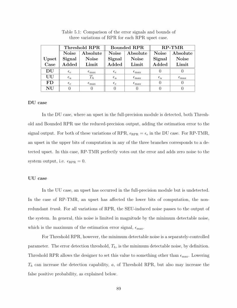
Table 5.1: Comparison of the error signals and bounds ofthree variations of RPR for each RPR upset case.
Threshold RPR Bounded RPR RP-TMRNoise Absolute Noise Absolute Noise Absolute
Upset Signal Noise Signal Noise Signal NoiseCase Added Limit Added Limit Added Limit
DU εe εmax εe εmax 0 0UU εu Th εu εmax εu εmax
FD εe εmax εe εmax 0 0NU 0 0 0 0 0 0
DU case
In the DU case, where an upset in the full-precision module is detected, both Thresh-
old and Bounded RPR use the reduced-precision output, adding the estimation error to the
signal output. For both of these variations of RPR, εRPR = εe in the DU case. For RP-TMR,
an upset in the upper bits of computation in any of the three branches corresponds to a de-
tected upset. In this case, RP-TMR perfectly votes out the error and adds zero noise to the
system output, i.e. εRPR = 0.
UU case
In the UU case, an upset has occurred in the full-precision module but is undetected.
In the case of RP-TMR, an upset has affected the lower bits of computation, the non-
redundant trunk. For all variations of RPR, the SEU-induced noise passes to the output of
the system. In general, this noise is limited in magnitude by the minimum detectable noise,
which is the maximum of the estimation error signal, εmax.
For Threshold RPR, however, the minimum detectable noise is a separately-controlled
parameter. The error detection threshold, Th, is the minimum detectable noise, by definition.
Threshold RPR allows the designer to set this value to something other than εmax. Lowering
Th can increase the detection capability, a, of Threshold RPR, but also may increase the
false positive probability, as explained below.
89
FD Case
For the FD case, there has been no upset in the full-precision module, yet the RPR
system mistakenly chooses the reduced-precision output. This can happen for both Thresh-
old RPR and Bounded RPR, but does not apply to RP-TMR: all upsets in the redundant
portion of the system are masked and all upsets in the non-redundant portion are classified
as UU events.
For Bounded RPR, the FD case can occur when there are upsets in the reduced-
precision modules. These are shown in Figure 5.5 as error cases 6 and 9, where an upset
in one of the bounding modules causes its output to cross the full-precision output, but
not the other bound’s output. These FD events reduce the overall performance of RPR by
introducing noise equal to εe at the RPR system output whenever these upsets occur, even
when no upset is present in the full-precision module.
Threshold RPR does not share this Bounded RPR problem. Any single upset affecting
the output of one of the two Threshold RPR reduced-precision modules causes a mismatch in
the comparison between the two reduced-precision modules in which case the full-precision
output is used. In fact, FD events can be completely eliminated by carefully setting the
error detection threshold.
For Threshold RPR, the false positive probability as used in Table 4.1 is:
Pfp = Pr(|FPout − RPout| > Th), (5.1)
or the probability of the difference between the full-precision and reduced-precision outputs
exceeding the set threshold in the absence of upsets. In order to avoid these false error
detection events, Th can be chosen such that RPout is never chosen in the absence of any
errors in the system by setting Th >= εmax.
Shim concluded that the optimal value for threshold is Th = εmax, in the general case.
A threshold for which Th > εmax prevents false positives, but is undesirable since upsets with
90
higher noise magnitude go undetected. On the other hand, Th < εmax adds the possibility of
an FD event, which add unnecessary noise to the system.
In this chapter, we set Th = εmax. This results in Pr(FD)= 0 for Threshold RPR and
simplifies the comparisons to the other types of RPR. However, Section 6.1 will discuss an
alternative approach that can lower Th while maintaining good performance.
NU Case
The NU case is simply the case in which there is no upset in the full-precision module
and there is no false positive error detection. All variations of RPR add no noise to the
system output in this case.
5.2.4 Error Detection Limits
The magnitude of the error that each RPR system can detect is another point in which
the three variations differ. The lookup table implementation used here for the constant
coefficient multiplier blocks gives Bounded RPR an advantage over Threshold RPR and
RP-TMR. The ability to set the error detection threshold (Th) manually, however, gives
Threshold RPR added flexibility.
As an example of these advantages, consider a constant coefficient multiplier module
with the reduced-precision replica implemented as an array multiplier for Threshold RPR
(or RP-TMR) and as a lookup table for Bounded RPR. Figures 5.12 and 5.13 illustrate the
error bounds of a sample RPR multiplier for Threshold and Bounded RPR, respectively.
Each RPR system is configured with B = 7, Br = 3, and a constant coefficient value of
h = 1/2− 2−B = 0.4921875 (a value fully representable by the full-precision module but not
the reduced-precision module).
Figure 5.12 shows the full-precision and reduced-precision module outputs for the
Threshold RPR multiplier. The error detection limits are simply the full-precision output
plus (and minus) the threshold value, Th. The error detection threshold is based on the
91

−0.75
−0.625
−0.5
−0.375
−0.25
−0.125
0
0.125
0.25
0.375
0.5
0.625
Multiplier input
Mul
tiplie
r out
put
−
1
−0.8
75
−0.
75
−0.6
25
−0.
5
−0.3
75
−0.
25
−0.1
25
0
0.1
25
0.2
5
0.3
75
0.
5
0.6
25
0.7
5
0.8
75
FPout+ThFPoutRPoutFPout−Th
Figure 5.12: Threshold RPR multiplier: full-precision output and reduced-precision outputwith error bounds. h = 0.4921875, B = 7, Br = 3, and Th = εmax
maximum quantization error of the full-precision and is constant for all multiplier inputs.
The error limits for an RP-TMR multiplier are the same when Th = εmax since the reduced
multiplier also has the architecture of a standard array multiplier as shown in Figure 5.10.
Figure 5.13 shows full-precision output and the error limits for the Bounded RPR
multiplier. Note that the error detection limits change depending on the multiplier input
value. The drawn grid shows the quantization of the reduced-precision inputs and outputs.
The output of the reduced-precision multiplier follows the full-precision output as closely
as the quantization limits allow. Also note that the worst case error for the Bounded RPR
multiplier is smaller than the worst case error for the Threshold RPR multiplier.
As discussed in Section 5.2.3, the error detection threshold of Threshold RPR is
configurable. Although setting Th = εmax guarantees that no false positive error detection
events will occur, Section 6.1 will show that a lower threshold is sometimes desirable. Thus
the configurability of this error detection limit can be an advantage of Threshold RPR.
92

−0.75
−0.625
−0.5
−0.375
−0.25
−0.125
0
0.125
0.25
0.375
0.5
0.625
Multiplier input
Mul
tiplie
r ou
tput
−
1
−0.
875
−0.
75
−0.
625
−0.
5
−0.
375
−0.
25
−0.
125
0
0.1
25
0.2
5
0.3
75
0.
5
0.6
25
0.7
5
0.8
75
−
1
−0.
875
−0.
75
−0.
625
−0.
5
−0.
375
−0.
25
−0.
125
0
0.1
25
0.2
5
0.3
75
0.
5
0.6
25
0.7
5
0.8
75
RPupper
FPout
RPlower
Figure 5.13: Bounded RPR multiplier: full-precision and reduced-precision outputs. h =0.4921875, B = 7, and Br = 3.
5.2.5 Suitability for FPGAs
In addition to other strengths and weaknesses, each type of RPR varies in its suit-
ability for FPGA implementation. In general, RPR lends itself well to use in FPGAs, as
demonstrated in Section 4.7. Some weaknesses are apparent in Bounded RPR and RP-TMR,
however. These issues are explained here and will be demonstrated in Section 5.3.
As mentioned in Section 4.2, the smaller reduced-precision modules in Shim’s RPR
system were not susceptible to VOS errors in ASIC systems. In contrast, the reduced-
precision modules in an FPGA system are still susceptible to SEUs. Threshold RPR and
RP-TMR handle this situation well and any upsets in the reduced-precision modules are
masked. SEUs in the reduced-precision modules in Bounded RPR, however, are not fully
masked, as explained in Section 5.2.3.
93

RP-TMR has a particular disadvantage in current FPGA technology in the nature of
its redundancy. Current FPGAs often contain fast carry chain logic to implement arithmetic
modules such as adders and multipliers. By necessity, RP-TMR interrupts this carry chain
in order to split the output of the trunk to drive the three upper branches of logic. This may
result in an increase in the critical path of the system and thus a decrease in its clock rate.
5.2.6 Summary
A summary of the relative strengths and weaknesses of the three variations of RPR
are presented here:
Threshold RPR
• Strengths:
– Straightforward implementation of reduced-precision modules
– Configurable error detection threshold (to eliminate false positive detection events
or increase performance)
• Weaknesses:
– Large decision block
– Static error detection threshold for all inputs (unlike Bounded RPR)
Bounded RPR
• Strengths:
– Tightest error detection limits (when using lookup tables as RP modules)
• Weaknesses:
– Large decision block
– Sensitive to false positive detection events
94

– Difficult to design reduced-precision modules as bounds (except when using lookup
tables, but these grow exponentially with the input bit width)
RP-TMR
• Strengths:
– Small decision block
– Only propagates errors in UU mode
– High potential for automated application of redundancy
• Weaknesses:
– No flexibility in reduced-precision module implementation
– Interrupts fast carry chain in current FPGAs
5.3 Fault Injection Experiments
This section presents fault injection experiments which were run in order to validate
the comparison presented above. Each variation of RPR will be applied to a communications
receiver and compared to the unmitigated design as well as a TMR version of the receiver.
These experiments will show the actual overhead cost and performance of each design in
the presence of SEUs. The results will also show to what extent each of the strengths and
weakness presented in Section 5.2 affect the overall system tested.
5.3.1 Experimental Configuration
To demonstrate and compare the performance of the three different RPR techniques,
several FIR filter designs of the form described in Section C.1 and shown in Figure C.1 were
implemented. For each type of RPR, an unmitigated FIR filter (B = 15) was taken and both
TMR and the RPR method was applied to it. For each RPR version, three levels of RPR
were applied using Br values of 3, 5, and 7 for the reduced-precision modules. Fault injection
95
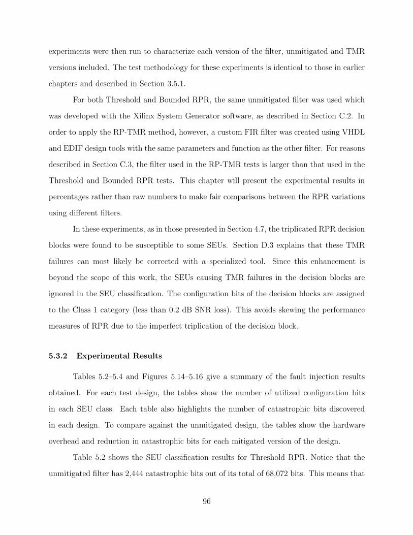
experiments were then run to characterize each version of the filter, unmitigated and TMR
versions included. The test methodology for these experiments is identical to those in earlier
chapters and described in Section 3.5.1.
For both Threshold and Bounded RPR, the same unmitigated filter was used which
was developed with the Xilinx System Generator software, as described in Section C.2. In
order to apply the RP-TMR method, however, a custom FIR filter was created using VHDL
and EDIF design tools with the same parameters and function as the other filter. For reasons
described in Section C.3, the filter used in the RP-TMR tests is larger than that used in the
Threshold and Bounded RPR tests. This chapter will present the experimental results in
percentages rather than raw numbers to make fair comparisons between the RPR variations
using different filters.
In these experiments, as in those presented in Section 4.7, the triplicated RPR decision
blocks were found to be susceptible to some SEUs. Section D.3 explains that these TMR
failures can most likely be corrected with a specialized tool. Since this enhancement is
beyond the scope of this work, the SEUs causing TMR failures in the decision blocks are
ignored in the SEU classification. The configuration bits of the decision blocks are assigned
to the Class 1 category (less than 0.2 dB SNR loss). This avoids skewing the performance
measures of RPR due to the imperfect triplication of the decision block.
5.3.2 Experimental Results
Tables 5.2–5.4 and Figures 5.14–5.16 give a summary of the fault injection results
obtained. For each test design, the tables show the number of utilized configuration bits
in each SEU class. Each table also highlights the number of catastrophic bits discovered
in each design. To compare against the unmitigated design, the tables show the hardware
overhead and reduction in catastrophic bits for each mitigated version of the design.
Table 5.2 shows the SEU classification results for Threshold RPR. Notice that the
unmitigated filter has 2,444 catastrophic bits out of its total of 68,072 bits. This means that
96

Table 5.2: Number of SEUs causing each class of effect for the FIR filter protected withfull TMR and Threshold RPR, compared against the unmitigated filter.
Total Total ImprovementSlices Slices Class 1 Class 2 Class 3 Class 4 Utilized Catastrophic in failure
Design Used Overhead Bits Bits Bits Bits Bits (% Reduction) rate
Unmitigated 1,030 - 59,156 6,472 1,501 943 68,072 2,444 (-%) -TMR 3,171 208% 218,304 0 0 2 218,306 2 (99.92%) 1,222×Thresh. RPR, Br = 7 1,755 70.4% 106,751 6,239 11 2 113,003 13 (99.47%) 188×Thresh. RPR, Br = 5 1,470 42.7% 84,284 7,819 226 2 92,331 228 (90.67%) 10.7×Thresh. RPR, Br = 3 1,313 27.5% 73,992 6,875 1,598 666 83,601 2,264 (7.36%) 1.1×
Table 5.3: Number of SEUs causing each class of effect for the FIR filter protected withfull TMR and Bounded RPR, compared against the unmitigated filter.
Total Total ImprovementSlices Slices Class 1 Class 2 Class 3 Class 4 Utilized Catastrophic in failure
Design Used Overhead Bits Bits Bits Bits Bits (% Reduction) rate
Unmitigated 1,030 - 59,156 6,472 1,501 943 68,072 2,444 (-%) -TMR 3,171 208% 218,304 0 0 2 218,306 2 (99.92%) 1,222×Bound. RPR, Br = 7 2,214 115% 123,720 4,746 0 1 128,467 1 (99.96%) 2,444×Bound. RPR, Br = 5 1,593 54.7% 88,121 9,957 88 1 98,167 89 (96.36%) 27.5×Bound. RPR, Br = 3 1,382 34.2% 75,817 7,189 3,037 423 86,466 3,460 (-41.57%) 0.7×
Table 5.4: Number of SEUs causing each class of effect for the FIR filter protected withfull TMR and RP-TMR, compared against the unmitigated filter.
Total Total ImprovementSlices Slices Class 1 Class 2 Class 3 Class 4 Utilized Catastrophic in failure
Design Used Overhead Bits Bits Bits Bits Bits (% Reduction) rate
Unmitigated 2,457 - 112,066 14,719 6,581 1,646 135,012 8,227 (-%) -TMR 7,351 199% 422,665 0 0 4 422,669 4 (99.95%) 2,056×RP-TMR, Br = 7 4,183 70.2% 228,910 302 135 1 229,348 136 (98.35%) 60.5×RP-TMR, Br = 5 3,587 46.0% 189,211 6,464 2,313 2 197,990 2,315 (71.86%) 3.6×RP-TMR, Br = 3 3,111 26.6% 150,751 13,056 3,323 20 167,150 3,343 (40.63%) 2.5×
97
over 96% of the configuration bits are likely to be protected through standard error handling
techniques at the application level.
The results from the filter designs with three levels of Threshold RPR (Br = 3, 5, 7)
are shown in this table. Each design has a hardware overhead significantly less than TMR
and each significantly reduces the number of catastrophic bits in the resulting design. The
RPR filter with Br = 5 (using 6-bit inputs to the reduced-precision modules), reduced the
number of catastrophic bits by over 90% at a cost of 43% on top of the cost of the original
filter. The RPR filter with Br = 7 eliminated nearly all of the catastrophic bits at a cost of
only 70%, about one-third that of TMR. In contrast, the RPR filter with Br = 3 was only
able to reduce the number of catastrophic bits by about 7%. Though the overhead of this
filter is very low, this bit-width appears to be too small to adequately protect this design.
Table 5.3 shows the SEU classification results for the filters with Bounded RPR
applied. The unmitigated and TMR results are repeated from Table 5.2 for ease of compar-
ison. Note that for the same Br value, Bounded RPR required more area than Threshold
RPR. This is not surprising given the lookup table implementation of the multipliers in this
implementation of Bounded RPR. For the RPR filter with Br = 5 and 7, Bounded RPR
performed slightly above Threshold RPR, as predicted by the slightly smaller error detection
limits shown in Section 5.2.4.
The Bounded RPR filter withBr = 3, however, performed very poorly, even increasing
the number of catastrophic SEUs over the unmitigated design. Recall that an upset in the
reduced-precision modules can affect the RPR output, as explained in Section 5.2.3, which
allows for this increase to occur. This adverse effect is not possible when using Threshold
RPR or RP-TMR, whose output are not affected by upsets in the reduced-precision modules.
Table 5.4 shows the SEU classification results for RP-TMR. Recall that the RP-TMR
test used a different unmitigated FIR filter than the Threshold and Bounded RPR tests and
uses a larger number of FPGA slices and configuration bits. The percentage of catastrophic
bits in this design, however, is similar: about 6.09%. The TMR version of the filter had a
98
similar overhead cost of about 200% and was able to eliminate nearly all of the catastrophic
bits.
The RP-TMR filters had a similar overhead cost to that of Threshold RPR in terms
of FPGA slices. Although RP-TMR does not require large, complex decision blocks like
Threshold RPR, the extra overhead is not seen in these experiments, where the decision
blocks are significantly smaller than the module being protected. The overhead in terms of
utilized configuration bits, however, was larger. Therefore, the additional sensitive area of
RP-TMR is likely due to additional configuration bits used for signal routing. This is not
unexpected due to the added routing congestion of RP-TMR, since the three upper branches
of logic are all dependent on the lower trunk logic and must be located physically close to
each other. In contrast, the three module replicas of Threshold and Bounded RPR are not
tied to each other at all and can be physically spread out.
RP-TMR did not provide the same protection against catastrophic SEUs as Threshold
RPR or Bounded RPR for the filters with Br = 5 and 7. RP-TMR actually exceeded the
performance of Threshold and Bounded RPR in the Br = 3 case in terms of percentage of
catastrophic SEUs mitigated. Although RP-TMR mitigated the Class 4 SEUs very well for
all bit-widths, it underperformed in preventing Class 3 SEUs in the Br = 5 and 7 designs.
It is not clear why RP-TMR did not mitigate these catastrophic upsets as well as the other
forms of RPR.
Figures 5.14–5.16 show the SNR loss values for all the designs tested. These figures
give a different view on the performance of the different types of RPR. While the distribution
of SEUs in the SNR loss cases shown is similar for Threshold and Bounded RPR, that of
RP-TMR is more favorable. Although RP-TMR did not perform as well with the high-noise
upsets, Figure 5.16 indicates that it performed better than Threshold and Bounded RPR
for lower-noise upsets, keeping the SNR loss lower on average. This is likely due to the
fact that, when RP-TMR is operating in reduced-precision mode, it uses both the upper and
lower bits of output—the output of the branches and the trunk, respectively. In contrast,
99
Threshold and Bounded RPR use only the truncated reduced-precision output, comparable
to only using the upper bits of the RP-TMR output.
> 0.2 dB > 0.5 dB > 1 dB > 3 dB > 6 dB0
2
4
6
8
10
12
14
16
18
SNR Loss
Nor
mal
ized
Per
cent
age
of U
pset
s
UnmitigatedRPR, B
r=3
RPR, Br=4
RPR, Br=5
Figure 5.14: Normalized percentage of SEUs causing certain SNR losses at BER of 10−5 foran FIR filter protected with three levels of Threshold RPR compared to the unmitigateddesign.
5.4 Summary
This chapter presented three different variations of reduced-precision redundancy.
Threshold RPR and Bounded RPR were previously suggested while RP-TMR is a new
technique introduced here. The preceding sections compared three types of RPR in several
aspects and fault injection experiments demonstrated each of the three techniques on a
simple communications receiver.
From the combination of the theoretical analysis and the experimental results pre-
sented here, the unique properties of each variation of RPR are summarizes as follows:
100

> 0.2 dB > 0.5 dB > 1 dB > 3 dB > 6 dB0
2
4
6
8
10
12
14
16
18
SNR Loss
Nor
mal
ized
Per
cent
age
of U
pset
s
UnmitigatedRPR, B
r=3
RPR, Br=4
RPR, Br=5
Figure 5.15: Normalized percentage of SEUs causing certain SNR losses at BER of 10−5
for an FIR filter protected with three levels of Bounded RPR compared to the unmitigateddesign.
RP-TMR is a straightforward way to protect the upper bits of computation. It
offers theoretically comparable error detection limits to Threshold RPR and uses significantly
smaller decision modules than either form of RPR. Its ability to use the lower-order bits of
computation even when the upper bits are in error gives it an advantage over the other
forms of RPR in some cases. As demonstrated, however, RP-TMR is not suitable for FPGA
implementation due to its additional timing cost and routing congestion.
Bounded RPR, as shown here and as suggested in previous work, obtains very small
error detection limits by implementing reduced-precision modules with lookup tables with
pre-computed contents. Bounded RPR, however, has an architectural flaw that allows for an
increase in sensitivity to catastrophic SEUs in some cases due to ambiguous error detection
cases. In general, the reduced-precision modules for this type of RPR are difficult to design.
101

> 0.2 dB > 0.5 dB > 1 dB > 3 dB > 6 dB0
2
4
6
8
10
12
14
16
18
SNR Loss
Nor
mal
ized
Per
cent
age
of U
pset
s
UnmitigatedRPR, B
r=3
RPR, Br=4
RPR, Br=5
Figure 5.16: Normalized percentage of SEUs causing certain SNR losses at BER of 10−5 foran FIR filter protected with three levels of RP-TMR compared to the unmitigated design.
Threshold RPR is relatively straightforward to implement and has a better decision
architecture than Bounded RPR in which false positive detection events can be completely
avoided. Also, although the static error comparison threshold resulted in higher average
error detection limits than Bounded RPR, this threshold is configurable and can be used to
enhance the performance of Threshold RPR.
In light of these results, Threshold RPR appears to be superior to the other two
variations of RPR. Chapter 6 will develop the Threshold RPR technique further. It will
present methods to select the Th and Br parameters to improve performance in the presence
of SEUs and reduce overhead cost.
102
CHAPTER 6. APPLICATION OF THRESHOLD RPR
Chapters 4 and 5 discussed many issues related to the implementation of RPR and
provided sample experimental results. These experiments were run simply to determine if
RPR could be suitable for these types of systems and to determine which variation of RPR
was best for FPGA systems. However, the RPR implementation details for these experiments
were chosen somewhat naıvely, without any detailed analysis of how RPR could best meet
the system requirements. This chapter provides a detailed look at several issues that need
to be addressed when designing a system with Threshold RPR.
Section 6.1 describes the benefits and drawbacks of lowering the error detection
threshold, Th. It presents a method for lowering Th which increases the SEU performance
of Threshold RPR in some cases. Fault injection experiments are presented to compare the
performance of the systems utilizing the standard and optimized Th values.
Section 6.2 discusses the effects of setting the bit-width of the reduced-precision mod-
ules, Br, in a Threshold RPR system. It describes how to determine the valid upper and
lower bounds on Br for a specific system. The section concludes with fault injection ex-
periments that demonstrate the effects of a wide range of Br values on a communications
receiver protected with Threshold RPR.
Section 6.3 provides insight into the design of Threshold RPR into more complex
systems. Until this point, RPR had been demonstrated only on simple modules and systems.
This section gives insight into several issues that must be considered when implementing
RPR on a recursive system with several different types of components. This section presents
a workflow for applying Threshold RPR to such a system. It concludes with a detailed
demonstration of mitigating SEUs in a recursive communications receiver using RPR.
103

6.1 Threshold Selection
As described in Section 5.1.1, Th is the error detection threshold of Threshold RPR.
Th is an important parameter which controls the magnitude of errors that are detected by
RPR. This value controls the noise limits of the RPR output.
In Chapter 5, Th was set to the maximum estimation error, εmax, as in previous work
by Shim. Shim’s Th value is the optimal value in the general case, where the probability
distribution of the estimation error signal is unknown. If the designer of a particular system
has additional information about this εe signal, however, a lower threshold value may be
offer better RPR performance.
This section describes the factors involved in setting the value of Th and suggests a
method for obtaining higher performance with a value of Th < εmax for a fixed Br value.
This novel method is made possible by limiting the scope of the RPR implementation to
a particular system and cannot offer higher performance for all systems. Fault injection
experiments then demonstrate the added benefit of these new Th values over the FIR filter
experiments presented in Section 5.3.
6.1.1 Average Threshold RPR Noise Limit
In order to summarize the effect of changing Th on the performance of the system,
we define an average noise limit for Threshold RPR, ERPR-avg. The average Threshold RPR
noise limit is based on the probabilities and noise limits of Table 4.1:
ERPR-avg = Pr(DU) · εmax + Pr(UU) · Th + Pr(FD) · εmax
= Pupset · a · εmax + Pupset · (1− a) · Th + (1− Pupset) · Pfp · εmax. (6.1)
This takes into account the probability of occurrence of each upset case and gives an average
value of the noise limit ERPR over time. This formula will be used to illustrate the ways in
which altering the Th value of the RPR system affects the performance of the system.
104
6.1.2 Reduction of Th
Recall that the value for Th affects both the distribution of UU and DU events as
well as the noise limits for each of these event types. This shift is represented by the change
in the value a in Equation 6.1.1 Increasing Th causes more UU events and fewer DU events,
decreasing a. Decreasing Th has the opposite effect. Decreasing Th also affects the noise
limit in the UU upset case. This makes it difficult to determine the overall effect of altering
Th on ERPR-avg.
A low value of Th (lower than εmax) is desirable because it lowers the noise limit in
the UU case. However, there are two possible disadvantages to a lower Th value:
1. There are possible false-positive error detection events, as discussed earlier. This in-
troduces noise equal to εe even when no upsets exist in the system.
2. Upsets that cause errors with magnitude above Th but below εmax are replaced with
the estimation error which has a bound at εmax. The resulting error, then, could be
larger than the error caused by the upset itself in some cases.
In each of these cases, the RPR system introduces a higher-magnitude noise than would
otherwise be present (in the unmitigated module). Each of these cases will now be described
in detail.
False Positive Error Events
In previous work, Th was set to the maximum estimation error, εmax. This value of Th
ensures that the false detection upset case did not occur. If the probability PFD is sufficiently
small, however, it may be desirable to lower Th to allow some false positive events. Knowledge
of the input signal characteristics or the operating environment could allow one to predict
PFD for lower Th values. Similarly, knowledge of the statistical properties of the εe signal
directly can provide enough information to be able to lower Th to obtain a better ERPR-avg.
1Table 6.5 in Section 6.1.4 reports on some measured values of the a factor for changing Th values.
105
In some cases, with knowledge of the input signal and the properties of a specific
module, it is possible to choose Th < εmax to avoid false positive detection events a large
portion of the time. In this case, PFD << 1, but may be non-zero. This alters the final term
in Equation 6.1, which is zero when using Th = εmax. However, the first and second terms
are also altered since the value a is dependent on Th and Th itself is the noise limit in the
UU case. Without knowing the value of a as a function of Th, it is difficult to predict the
effect on ERPR-avg. This function is dependent on the module being protected and the upset
environment and is difficult to generalize.
A more direct method is to examine the distribution of the estimation error signal, εe.
Shim showed that, for a uniformly-distributed εe signal, the optimal value for Th is εmax [47].
This is reasonable because all values of εe between 0 and εmax are equally probable, including
those above any value Th less than εmax. Thus Pfp increases sharply as Th is lowered below
εmax. This, in turn, increases the frequency of the FD upset event which decreases the overall
performance of RPR.
If, on the other hand, the distribution of the εe signal is such that higher values of εe
are less probable than lower values, the increase in Pfp may not be enough to severely affect
the performance of the system. For example, if the distribution of εe is Gaussian,2 the false
error probability can be predicted based on the relation of Th to the standard deviation (σ)
of the distribution. Table 6.1 shows the relation of Pfp to Th for this case. A system with
Th = σ can expect a false positive every third clock cycle, on average. Values of Th = 5σ
and Th = 6σ, however, result in false positive error rates of less than 10−6. With rates this
low, it can certainly be feasible to lower Th without fear of significantly increasing the FD
upset case probability.
The distribution of εe is highly dependent on the type of module being protected as
well as the signal environment at its input. For example, a simple register with a uniformly-
distributed input would have a uniformly-distributed εe signal due to the simple truncation
2The actual εe signal cannot be a true Gaussian, of course. The εe signal has an actual cutoff at εmax
while a true Gaussian distribution has infinite support.
106
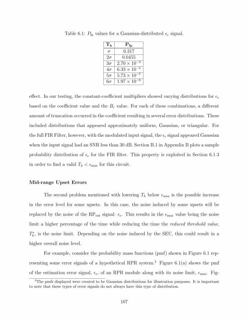
Table 6.1: Pfp values for a Gaussian-distributed εe signal.
Th Pfp
σ 0.3172σ 0.04553σ 2.70× 10⁻³
4σ 6.33× 10⁻⁵
5σ 5.73× 10⁻⁷
6σ 1.97× 10⁻⁹
effect. In our testing, the constant-coefficient multipliers showed varying distributions for εe
based on the coefficient value and the Br value. For each of these combinations, a different
amount of truncation occurred in the coefficient resulting in several error distributions. These
included distributions that appeared approximately uniform, Gaussian, or triangular. For
the full FIR Filter, however, with the modulated input signal, the εe signal appeared Gaussian
when the input signal had an SNR less than 30 dB. Section B.1 in Appendix B plots a sample
probability distribution of εe for the FIR filter. This property is exploited in Section 6.1.3
in order to find a valid Th < εmax for this circuit.
Mid-range Upset Errors
The second problem mentioned with lowering Th below εmax is the possible increase
in the error level for some upsets. In this case, the noise induced by some upsets will be
replaced by the noise of the RPout signal: εe. This results in the εmax value being the noise
limit a higher percentage of the time while reducing the time the reduced threshold value,
T ∗h , is the noise limit. Depending on the noise induced by the SEU, this could result in a
higher overall noise level.
For example, consider the probability mass functions (pmf) shown in Figure 6.1 rep-
resenting some error signals of a hypothetical RPR system.3 Figure 6.1(a) shows the pmf
of the estimation error signal, εe, of an RPR module along with its noise limit, εmax. Fig-
3The pmfs displayed were created to be Gaussian distributions for illustration purposes. It is importantto note that these types of error signals do not always have this type of distribution.
107
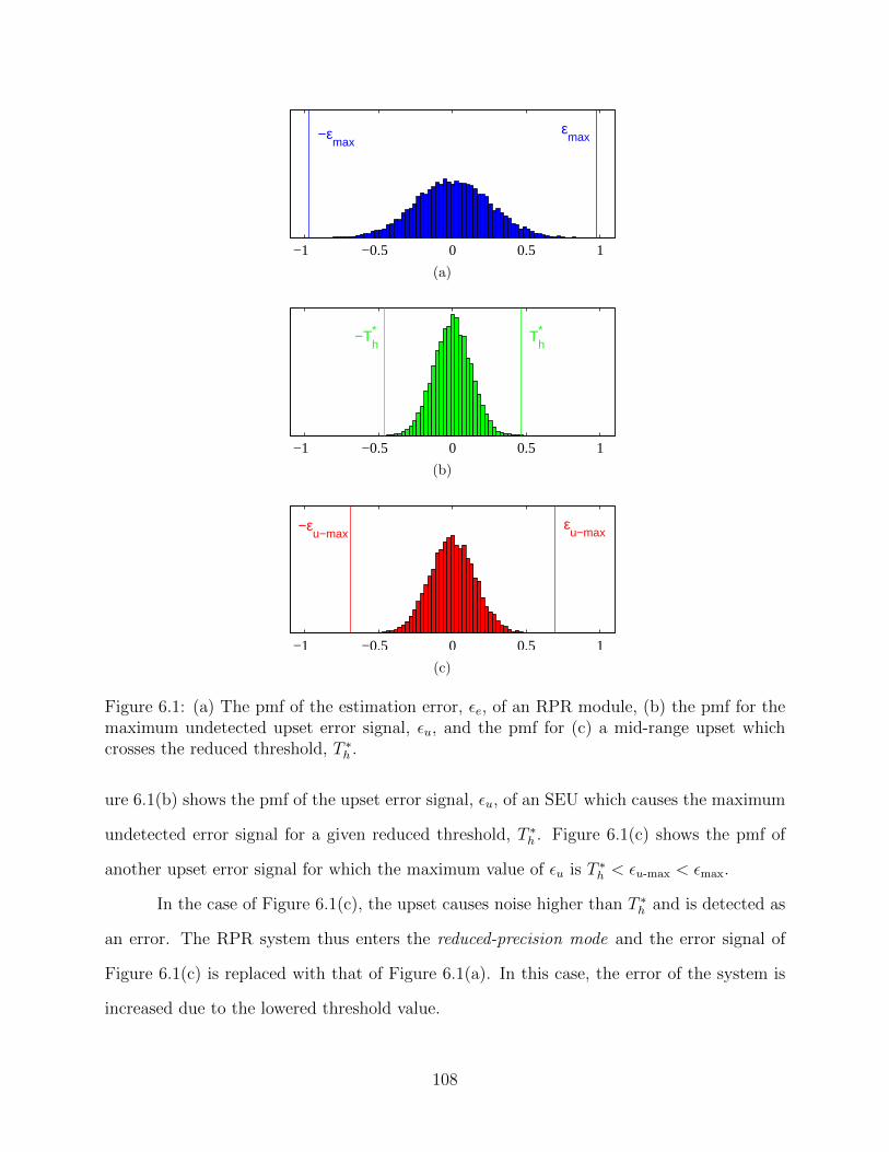
−1 −0.5 0 0.5 1
εmax−ε
max
(a)
−1 −0.5 0 0.5 1
Th*−T
h*
(b)
−1 −0.5 0 0.5 1
εu−max−ε
u−max
(c)
Figure 6.1: (a) The pmf of the estimation error, εe, of an RPR module, (b) the pmf for themaximum undetected upset error signal, εu, and the pmf for (c) a mid-range upset whichcrosses the reduced threshold, T ∗
h .
ure 6.1(b) shows the pmf of the upset error signal, εu, of an SEU which causes the maximum
undetected error signal for a given reduced threshold, T ∗h . Figure 6.1(c) shows the pmf of
another upset error signal for which the maximum value of εu is T ∗h < εu-max < εmax.
In the case of Figure 6.1(c), the upset causes noise higher than T ∗h and is detected as
an error. The RPR system thus enters the reduced-precision mode and the error signal of
Figure 6.1(c) is replaced with that of Figure 6.1(a). In this case, the error of the system is
increased due to the lowered threshold value.
108

This discussion shows that the effect of lowering Th below εmax can have mixed conse-
quences. With additional knowledge about a specific system (including characteristics of the
input signal, SEU-induced noise, and estimation error) it would be possible to pre-determine
the optimal value for Th. In the end, however, the most general acceptable rule is that Th
should not be lowered below εmax. With that in mind, the following section introduces a
method for finding an acceptable lower value for Th experimentally.
6.1.3 Experimental Determination of Th
Although lowering the value of Th below εmax can have negative consequences, these
negative effects only occur during time periods when Th < εe < εmax. The value of εmax
is determined mathematically based on the structure of the module in question and the
possible input signals. This section shows that it is possible to determine an acceptable
tighter bound on εe experimentally. For some modules, the practical maximum value of εe
can be significantly lower than the theoretical value. Section 6.1.4 will then demonstrate the
RPR performance gains that can be achieved by basing Th on this lower value.
Recall the following definition from Section 4.4:
εmax = max |εe| = max |FPtrue − RPout|. (6.2)
The value of εmax was determined mathematically for several simple modules for several
types of RPR. This determination was done with the theoretical maximum error values for
each module. The values of εmax for the register, adder, and multiplier were then combined
to form εmax for an FIR filter.
Although the theoretical maximum values for these modules are accurate, meaning
there is some input sequence that can produce the maximum value given, there was no notion
given of their probability of occurrence. For simple components and known input signal
characteristics, the probability of the maximum estimation error (Pr(εe = εmax)) or the
109

probability of any value above a certain threshold (Pr(εe > T ∗h )) can be easily determined.
For more complex modules, or for combinations of simple modules such as the FIR filter in
Figure 3.6, these probabilities can be much more difficult to calculate theoretically.
If, under known conditions, the probability Pr(εe > T ∗h ) for a chosen threshold, T ∗
h is
very close to zero, it may be desirable to use T ∗h as the RPR detection threshold Th. If this
probability is sufficiently close to zero, we may use the same assumptions as if we had used
Th = εmax, namely that Pr(FD) = 0 and that the noise in the FD error case will never be
larger than the upset noise. The measure of sufficiently close to zero is subjective and tied
to the system in question. In a communications system where there is a BER requirement
of 10−5 at a certain SNR, the value of Pr(FD) should be low enough such that FD events
cause bit errors well below that rate.
Rather than using the theoretical value, as suggested by Shim, the maximum value
of εe can be determined experimentally. We label this experimentally-determined value ε∗max,
which is used to determine the experimental decision threshold labeled T ∗h , where ε∗max < εmax
and T ∗h < Th. An experimentally-determined threshold, of course, is only valid for a specific
circuit. Without a specific assumption like this, Shim’s Th = εmax is the correct value to use.
For the FIR filter circuit, we have experimentally measured the signal εe for several
different RPR bit-widths. To do this, we created bit-accurate simulation models of the full-
precision and reduced-precision FIR filter circuits using Matlab. We then generated several
representative modulated input signals, each with a different SNR level (SNR values of 2, 4,
6, 8, and 10 dB). These models were then used as follows:
1. Each of the input signals was processed by the FP filter and the output signals recorded
2. The same input signals were processed by each RP filter and the output signals recorded
3. For each RP filter and each SNR, the estimation error signal, εe, was calculated
4. The absolute maximum value of each εe signal was recorded as ε∗max
5. The mean (µe) and standard deviation (σe) of each εe signal were calculated
110

For this design and these input characteristics, the signal εe was roughly Gaussian-
distributed. As expected, the ε∗max value was dependent on the test duration. We also
discovered that the SNR of the input signal did not have a significant impact on the statistics
of the εe signal. Section B.1 in Appendix B plots the probability mass functions (pmfs) for
the FIR filter design with various bit-widths at an SNR of 8 dB, demonstrating this Gaussian
distribution and the effect of changing Br.
Using the Gaussian distribution of εe and the values in Table 6.1 as a hint, we calcu-
lated the experimental threshold as:
T ∗h = µe + 6σe. (6.3)
We confirmed this to be a valid threshold (i.e. T ∗h > ε∗max) for simulation durations up to 106
samples. With this value of T ∗h , we expected Pfp to be very low, as suggested by Table 6.1.
Table 6.2 shows the different threshold values obtained for several different reduced-
precision FIR filters. Both the theoretical (Th) and experimental (T ∗h ) threshold values are
shown for each filter as well as the mean (µ) and standard deviation (σ) values for the signal
εe. Notice that the experimentally-determined values, in these cases, become increasingly
lower than their theoretical counterparts as Br decreases. This can greatly increase the
number of errors detected for a particular bit-width and has the potential to make even
lower Br values feasible for a particular system.
Table 6.2: Mathematical (Th) vs. experimental (T ∗h ) threshold values for RPR FIR filter
designs with several different reduced-precision bit-widths (Br). The mean (µe)and standard deviation (σe) values for the signal εe are also shown.
Br Th T∗h % Change µe σe
7 0.1597 0.1049 −34.3% 0.3659 0.094656 0.3106 0.1844 −40.6% 0.2453 0.05625 0.6046 0.3182 −47.4% 0.1431 0.028914 1.2212 0.5849 −52.1% 0.08365 0.015633 2.3871 0.9222 −61.4% 0.05380 0.008500
111
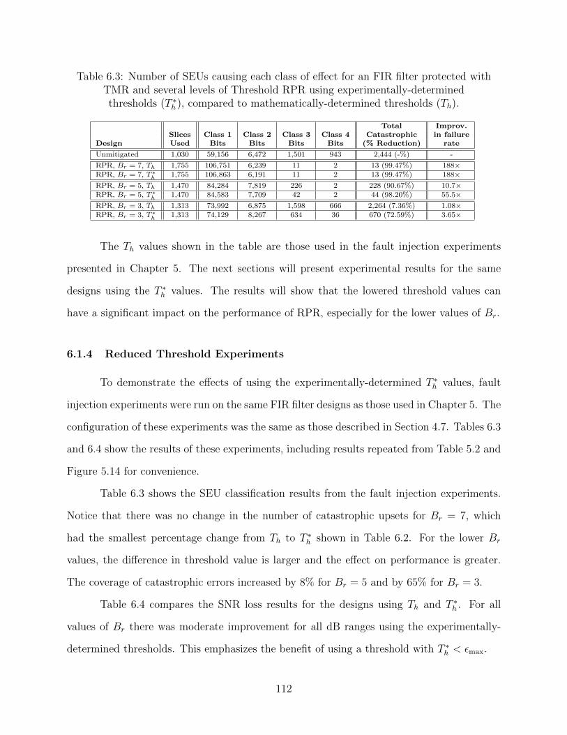
Table 6.3: Number of SEUs causing each class of effect for an FIR filter protected withTMR and several levels of Threshold RPR using experimentally-determinedthresholds (T ∗
h ), compared to mathematically-determined thresholds (Th).
Total Improv.Slices Class 1 Class 2 Class 3 Class 4 Catastrophic in failure
Design Used Bits Bits Bits Bits (% Reduction) rate
Unmitigated 1,030 59,156 6,472 1,501 943 2,444 (-%) -
RPR, Br = 7, Th 1,755 106,751 6,239 11 2 13 (99.47%) 188×RPR, Br = 7, T ∗
h 1,755 106,863 6,191 11 2 13 (99.47%) 188×RPR, Br = 5, Th 1,470 84,284 7,819 226 2 228 (90.67%) 10.7×RPR, Br = 5, T ∗
h 1,470 84,583 7,709 42 2 44 (98.20%) 55.5×RPR, Br = 3, Th 1,313 73,992 6,875 1,598 666 2,264 (7.36%) 1.08×RPR, Br = 3, T ∗
h 1,313 74,129 8,267 634 36 670 (72.59%) 3.65×
The Th values shown in the table are those used in the fault injection experiments
presented in Chapter 5. The next sections will present experimental results for the same
designs using the T ∗h values. The results will show that the lowered threshold values can
have a significant impact on the performance of RPR, especially for the lower values of Br.
6.1.4 Reduced Threshold Experiments
To demonstrate the effects of using the experimentally-determined T ∗h values, fault
injection experiments were run on the same FIR filter designs as those used in Chapter 5. The
configuration of these experiments was the same as those described in Section 4.7. Tables 6.3
and 6.4 show the results of these experiments, including results repeated from Table 5.2 and
Figure 5.14 for convenience.
Table 6.3 shows the SEU classification results from the fault injection experiments.
Notice that there was no change in the number of catastrophic upsets for Br = 7, which
had the smallest percentage change from Th to T ∗h shown in Table 6.2. For the lower Br
values, the difference in threshold value is larger and the effect on performance is greater.
The coverage of catastrophic errors increased by 8% for Br = 5 and by 65% for Br = 3.
Table 6.4 compares the SNR loss results for the designs using Th and T ∗h . For all
values of Br there was moderate improvement for all dB ranges using the experimentally-
determined thresholds. This emphasizes the benefit of using a threshold with T ∗h < εmax.
112

Table 6.4: Normalized percentage of SEUs causing certain SNR losses at BER of 10−5
for an FIR filter protected with several levels of Threshold RPR usingexperimentally-determined thresholds (T ∗
h ), compared tomathematically-determined thresholds (Th).
Design > 0.2 dB > 0.5 dB > 1 dB > 3 dB > 6 dB
Unmitigated 13.1% 10.6% 9.07% 6.29% 5.32%
RPR, Br = 7, Th 9.19% 3.29% 1.62% 0.0191% 0.0191%RPR, Br = 7, T ∗
h 9.11% 2.48% 0.696% 0.0191% 0.0191%
RPR, Br = 5, Th 11.8% 9.16% 7.23% 3.08% 1.62%RPR, Br = 5, T ∗
h 11.39% 8.85% 6.89% 1.51% 0.602%
RPR, Br = 3, Th 13.4% 10.7% 8.97% 5.98% 5.01%RPR, Br = 3, T ∗
h 13.1% 10.3% 8.50% 5.47% 3.71%
Table 6.5: Detection factor (a) for an FIR filter protected with several levels ofThreshold RPR using experimentally-determined thresholds (T ∗
h ), comparedto mathematically-determined thresholds (Th) at an SNR of 8 dB.
Design a
RPR, Br = 7, Th 0.0754RPR, Br = 7, T ∗
h 0.1082
RPR, Br = 5, Th 0.0519RPR, Br = 5, T ∗
h 0.0859
RPR, Br = 3, Th 0.0495RPR, Br = 3, T ∗
h 0.0699
Table 6.5 reports on measured values of the RPR detection factor, a, for both thresh-
old values. This value is the fraction of upsets in the full-precision module that were detected
by the RPR system and for which the reduced-precision output was used. Note that, as ex-
pected, the a factor increases with the lower threshold T ∗h for each Br value.
6.2 Bit-width Selection
The previous section discussed setting Th for a fixed reduced-precision bit-width,
Br. This section presents the considerations necessary when setting Br. The value of Br
determines the quality of the estimate that the reduced-precision modules produce relative
113
to the full-precision module. This in turn controls the valid range of Th and the level of noise
that is detectable by the system.
In general, a higher Br has a higher area cost and gives better performance. The
effect on performance can be seen in Equation 6.1: since both εmax and Th decrease with an
increase in Br, the average noise limit of Threshold RPR decreases as well.
This section emphasizes that the selection of Br has a large impact on the performance
and cost of RPR. It describes this impact and presents how to calculate the valid range of
Br available for a particular module. It also demonstrates the trade-offs between the cost
and performance factors with fault injection experiments.
6.2.1 Bit-width Effects
The primary effect of setting Br is to set the accuracy of the estimate of the full-
precision module and thus the estimation error signal, εe. This affects the noise of the
system in reduced-precision mode, but also the level of SEU-induced noise that is detectable.
Effect on Performance
The Br value directly sets the noise level of the RPR system while in reduced-precision
mode. RPR operates in this mode when an error is detected in the full-precision module and
the reduced-precision output is used. Thus the noise level in this mode depends solely on
the performance of the reduced-precision module and upon its bit-width.
For example, Figure 6.2 shows several BER curves for the binary PAM system de-
scribed in Section 3.5, each for an FIR filter with a different input bit-width. If one of
the application requirements specifies that the BER in reduced-precision mode should be at
most 10−4 at an SNR of 10 dB, the input bit-width of the RP modules must be Br ≥ 5.
The Br value also controls the level of SEU-induced noise that is detectable. A
smaller Br value means the reduced-precision module produces a poorer estimate of the full-
114

0 2 4 6 8 10 1210
−10
10−8
10−6
10−4
10−2
100
Eb/N
o
BE
R
TheoreticalB
r=1
Br=2
Br=3
Br=4
Br=5
Br=6
Br=7
Br=8
Figure 6.2: Bit error rate curves for several FIR filters (SRRC pulse shape, α = 0.5) withdifferent bit-widths.
precision output, resulting in a larger possible difference between the two outputs. Thus a
higher threshold, Th, is needed for a smaller Br.
Effect on Error Detection Threshold
Lowering the Br value decreases the performance of an RPR system, resulting in a
cutoff of its usefulness as Br approaches zero. As Br is lowered, Th must become larger.
Obviously, there are few interesting circuits that would be estimated well by a reduced-
precision module with Br = 0 (a 1-bit signed number). Depending on the application, the
value for Th could become too large to be usable at Br values significantly higher than 0.
Using the feed-forward binary PAM system as an example, the output of the full-
precision FIR filter has a bit-width of Q1.15, giving it a possible range of [-2,2). From
Table 6.2, the theoretical value of Th for Br = 3 is 2.3871. This is over 50% of the total
115
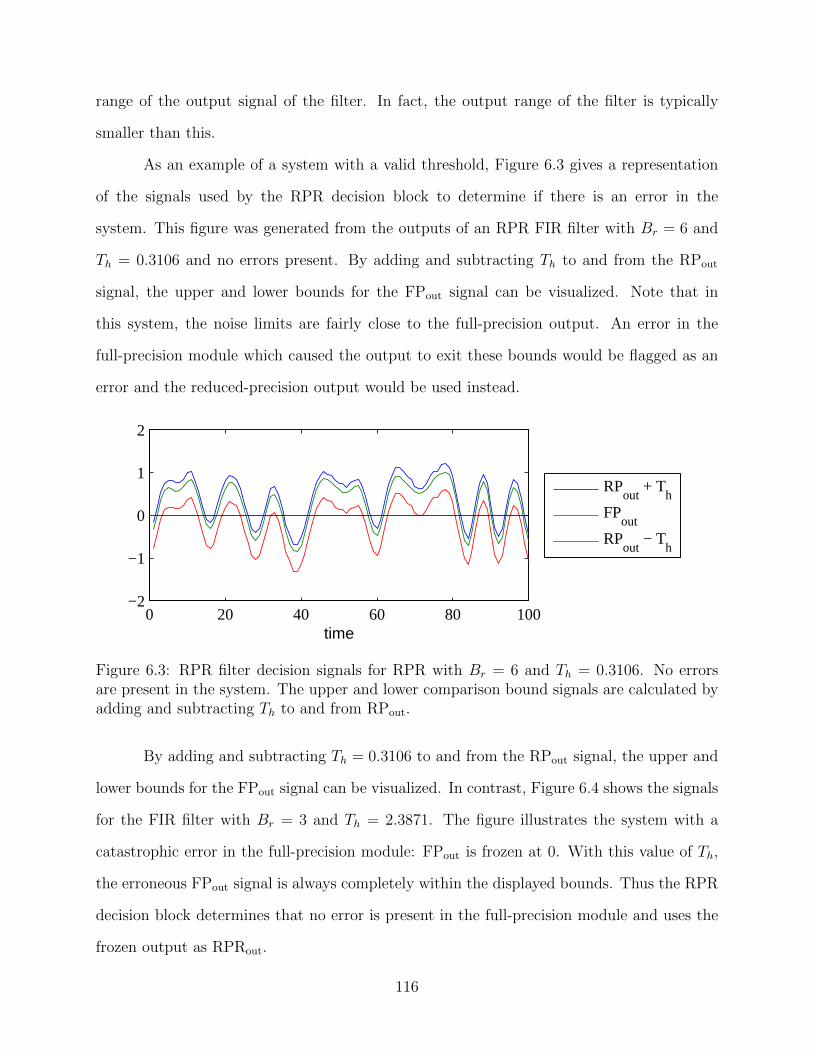
range of the output signal of the filter. In fact, the output range of the filter is typically
smaller than this.
As an example of a system with a valid threshold, Figure 6.3 gives a representation
of the signals used by the RPR decision block to determine if there is an error in the
system. This figure was generated from the outputs of an RPR FIR filter with Br = 6 and
Th = 0.3106 and no errors present. By adding and subtracting Th to and from the RPout
signal, the upper and lower bounds for the FPout signal can be visualized. Note that in
this system, the noise limits are fairly close to the full-precision output. An error in the
full-precision module which caused the output to exit these bounds would be flagged as an
error and the reduced-precision output would be used instead.
0 20 40 60 80 100−2
−1
0
1
2
time
RPout
+ Th
FPout
RPout
− Th
Figure 6.3: RPR filter decision signals for RPR with Br = 6 and Th = 0.3106. No errorsare present in the system. The upper and lower comparison bound signals are calculated byadding and subtracting Th to and from RPout.
By adding and subtracting Th = 0.3106 to and from the RPout signal, the upper and
lower bounds for the FPout signal can be visualized. In contrast, Figure 6.4 shows the signals
for the FIR filter with Br = 3 and Th = 2.3871. The figure illustrates the system with a
catastrophic error in the full-precision module: FPout is frozen at 0. With this value of Th,
the erroneous FPout signal is always completely within the displayed bounds. Thus the RPR
decision block determines that no error is present in the full-precision module and uses the
frozen output as RPRout.
116
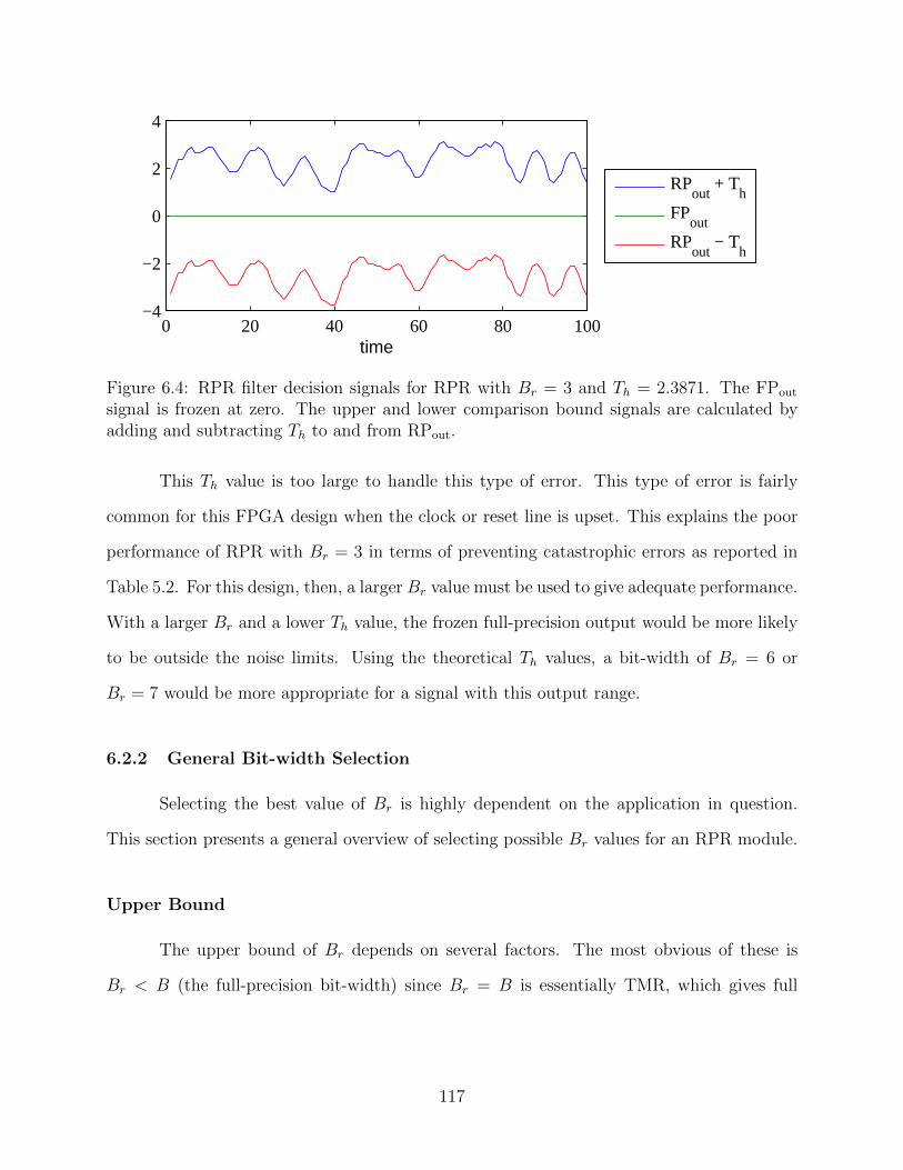
0 20 40 60 80 100−4
−2
0
2
4
time
RPout
+ Th
FPout
RPout
− Th
Figure 6.4: RPR filter decision signals for RPR with Br = 3 and Th = 2.3871. The FPout
signal is frozen at zero. The upper and lower comparison bound signals are calculated byadding and subtracting Th to and from RPout.
This Th value is too large to handle this type of error. This type of error is fairly
common for this FPGA design when the clock or reset line is upset. This explains the poor
performance of RPR with Br = 3 in terms of preventing catastrophic errors as reported in
Table 5.2. For this design, then, a larger Br value must be used to give adequate performance.
With a larger Br and a lower Th value, the frozen full-precision output would be more likely
to be outside the noise limits. Using the theoretical Th values, a bit-width of Br = 6 or
Br = 7 would be more appropriate for a signal with this output range.
6.2.2 General Bit-width Selection
Selecting the best value of Br is highly dependent on the application in question.
This section presents a general overview of selecting possible Br values for an RPR module.
Upper Bound
The upper bound of Br depends on several factors. The most obvious of these is
Br < B (the full-precision bit-width) since Br = B is essentially TMR, which gives full
117

protection against single upsets. Even values close to B are undesirable due to the increased
overhead of the RPR decision blocks compared to TMR voters.
Another simple upper bound is an area or power limit imposed by application con-
straints. Besides the area and power costs of higher Br values, there is no general downside to
increased precision in the reduced-precision modules. This can only increase the performance
of the system.
Lower Bound
The lower bound of Br is determined by when the detection capabilities of RPR
degrade to unusable levels. Section 6.2.1 described an example where the Br value caused
the Th value to increase such that critical errors went undetected. Similar methods can be
used for other systems.
In a more general sense, the Th value is the general noise limit on the RPR system,
as seen in Equation (6.1). The designer of the RPR module can thus define an acceptable
noise limit at the output of the RPR decision block and increase Br until the calculated or
measured value of Th falls below this bound.
Optimization
These bounds, of course, are only a starting point for selecting Br for a particular
module. At this point, the designer must find the optimal trade-off between the cost of im-
plementation and the performance of the system. If the upset rate of the target environment
is very low, ERPR-avg will be small even with a low Br value. If the upset rate is higher, it
may be more important to use a high Br value to keep the noise low in the DU upset case.
For example, Figure 6.5 plots the value of ERPR-avg of the FIR filter design for several
bit-widths in two different upset environments: GPS orbit and Polar orbit. If the target
ERPR-avg for this system is 10−6, the system in the Polar orbit requires a Br of 5. With the
118

higher upset rate of the GPS orbit, however, the system requires a Br of at least 7 to meet
the noise limit target.
3 4 5 6 710
−7
10−6
10−5
Br
ER
PR
−av
g
GPS orbitPolar orbitError Target
Figure 6.5: ERPR-avg of the FIR filter design for several bit-widths and using two failurerates.
In this case, using ERPR-avg as the measure of performance of the RPR system, the
upsets are not frequent enough in the Polar orbit to warrant a high cost of RPR. In the GPS
orbit, however, the RPR system is predicted to enter reduced-precision mode much more
often, increasing ERPR-avg significantly.
The effects of these trade-offs are highly dependent on the application in question and
cannot be generalized. What is important is that RPR can give many options for increasing
the performance of a system in the presence of SEUs. The next section presents results from
fault injection experiments that demonstrate these options which trade-off circuit area for
performance.
119
6.2.3 Bit-width Experiments
In order to demonstrate the effects of varying the reduced-precision bit-width (Br)
for Threshold RPR, the previous fault injection experiments were expanded. This section
reports on the performance of the simple feed-forward communications system of Section 5.3
for Br = 3–7. The designs tested used the experimentally-determined thresholds T ∗h in
Table 6.2. The results emphasize the flexibility of RPR by demonstrating the wide range of
cost and performance trade-off points that Threshold RPR offers this system.
Table 6.6 shows the SEU classification results from the fault injection experiments.
As expected, increasing the bit-width of the reduced-precision filters improved the handling
of catastrophic SEUs. The cost of implementation increased with Br as well.
Figure 6.6 plots the SNR loss values for the various versions of this filter. Notice that
the increase in Br does more than increase the design’s resistance to catastrophic SEUs. As
the size of the reduced-precision filters increases, the number of higher-noise SEUs decreases
as well. As expected, the more costly the RPR system, the lower the overall noise and the
higher the performance.
Again, TMR was much more effective at protecting the receiver system against SEUs
than RPR in our experiments. In the case of the RPR implementation with Br = 6, the
overhead cost of implementing RPR was about one-quarter that of TMR. This version of
RPR reduced the number of catastrophic bits by over 99% and significantly reduced the
number of high-noise SEUs. Although the RPR implementation with Br = 7 did not offer
any improvement in protection against catastrophic SEUs over the Br = 6 design, Figure 6.6
reflects the improvements in SNR loss offered by the extra hardware required. Even the
implementation with Br = 3 offers a significant improvement. At a cost of only 28% more
hardware, the number of catastrophic bits decreased by over 70%.
These results emphasize that RPR offers flexibility in its implementation options. It
is fairly straightforward to increase the performance of an RPR system in the presence of
SEUs by increasing the amount of redundancy in the reduced-precision modules. The range
120

Table 6.6: Number of SEUs causing each class of effect for an FIR filter protected with TMR and several levels ofThreshold RPR using experimentally-determined thresholds (T ∗
h ), compared to the unmitigated filter.
Total Total Improv.Slices Slices Class 1 Class 2 Class 3 Class 4 Utilized Catastrophic in failure
Design Used Overhead Bits Bits Bits Bits Bits (% Reduction) rate
Unmitigated 1,030 - 59,156 6,472 1,501 943 68,072 2,444 (-%) -
TMR 3,171 208% 218,304 0 0 2 218,306 2 (99.92%) 1222×RPR, Br = 7 1,755 70.4% 106,863 6,191 11 2 113,067 13 (99.47%) 188×RPR, Br = 6 1,602 55.5% 95,980 7,731 9 2 103,722 11 (99.55%) 222×RPR, Br = 5 1,470 42.7% 84,583 7,709 42 2 92,336 44 (98.20%) 55.5×RPR, Br = 4 1,394 35.3% 79,334 8,252 254 2 87,842 256 (89.53%) 9.55×RPR, Br = 3 1,313 27.5% 74,129 8,267 634 36 83,066 670 (72.59%) 3.65×
121
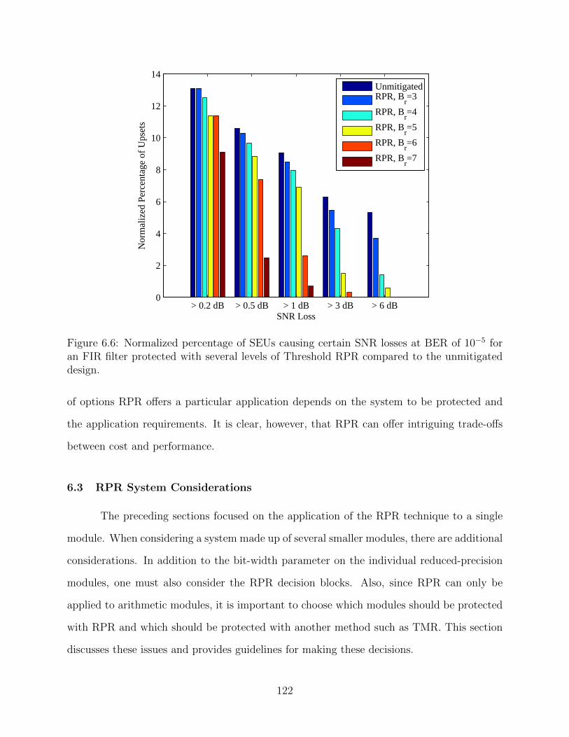
> 0.2 dB > 0.5 dB > 1 dB > 3 dB > 6 dB0
2
4
6
8
10
12
14
SNR Loss
Nor
mal
ized
Per
cent
age
of U
pset
s
UnmitigatedRPR, B
r=3
RPR, Br=4
RPR, Br=5
RPR, Br=6
RPR, Br=7
Figure 6.6: Normalized percentage of SEUs causing certain SNR losses at BER of 10−5 foran FIR filter protected with several levels of Threshold RPR compared to the unmitigateddesign.
of options RPR offers a particular application depends on the system to be protected and
the application requirements. It is clear, however, that RPR can offer intriguing trade-offs
between cost and performance.
6.3 RPR System Considerations
The preceding sections focused on the application of the RPR technique to a single
module. When considering a system made up of several smaller modules, there are additional
considerations. In addition to the bit-width parameter on the individual reduced-precision
modules, one must also consider the RPR decision blocks. Also, since RPR can only be
applied to arithmetic modules, it is important to choose which modules should be protected
with RPR and which should be protected with another method such as TMR. This section
discusses these issues and provides guidelines for making these decisions.
122
6.3.1 RPR Decision Blocks
RPR decision blocks, or RPR voters, must be used to resolve the outputs of the full-
precision and reduced-precision outputs into a single output. The number and placement
of voters in a TMR- or RPR-mitigated system can have a large effect on the reliability and
cost of that system [45], [75]–[78]. RPR voters are needed for all types of RPR, though their
complexity varies. The voters required for Threshold and Bounded RPR are more costly
than those of RP-TMR, requiring approximately 8–9 times more logic.
Voter Count and Placement
When several reduced-precision modules are connected, the quantization noise of
each contributes to the total quantization noise at the output. In essence, the maximum
quantization error of a simple module is generally less than a more complex module. Sullivan
noted the effects of these “compound operations” in her thesis and calculated the increased
bounds needed for some sample operations [64].
In the extreme cases RPR voters could be placed: 1) at the output of every individual
arithmetic module or 2) only at the final output of the system. With voters at the output of
every module, either Br or Th could be lowered for each module and decision block. With a
voter at only at the output of the system, either Br or Th must be increased to account for
the extra quantization error accumulated through multiple reduced-precision modules.
As an example of the trade-offs involved in selecting the number and locations of
voters, consider the 4-tap FIR filter illustrated in Figure 6.7. Section D.2 estimates the cost
of this circuit with several different voter configurations:
1. RPR voters at the output of each multiplier
2. Triplicated RPR voters at the output of each multiplier
3. A single RPR voter at the output of the filter
4. One triplicated RPR voter at the output of the filter
123

In each case, the RPR voters use Shim’s optimized architecture. The appendix shows that,
when moving the voters from the multiplier outputs to the filter output, the bit-width of
the reduced-precision modules must increase in order to maintain the same error detection
limit, Th.
Figure 6.7: Block diagram of a 4-tap FIR filter.
Using the resource utilization tables in Appendix E, the estimates of these configura-
tions are shown in Table 6.7. In this example, the cost of each system is nearly equal in the
case of optimized, non-triplicated voters. If the voters are to be protected from SEUs as well,
however, the cost of the first system is significantly higher. In this case it is preferable to
increase the bit-widths of the reduced-precision modules rather than add more RPR decision
blocks in order to maintain the same threshold.
Table 6.7: Estimated cost of several 4-tap FIR filter circuits protected with RPR.
Single TriplicatedVoter Locations Voters Voters
After multipliers 1,169 1,609At filter output 1,157 1,245
This analysis is a simple example and will certainly be different for each system
considered. In general, however, it is important to consider the number and position of the
124

RPR decision blocks in a digital system. There is a trade-off between the accumulation of
quantization noise and the area cost of more voters.
Suggested Workflow for Placing RPR Decision Blocks
A reasonable starting point for selecting the number and location of RPR voters is
to constrain the noise in the system by limiting the noise limit or Th value at a certain point
in the circuit. The simplistic approach places one RPR decision block at that point in the
circuit and calculates the necessary Br values of the components leading up to that point
to achieve that Th value. If there are many components leading to that point, however, the
Br values required may be very large. As an optimization step, one or more RPR decision
blocks could be added to the system. This can reduce the strain on the initial decision block
and allow smaller Br values, reducing the cost of the reduced-precision modules.
Figure 6.8 presents the workflow diagram for this process. As suggested above, the
first time through the loop, a single decision block, or voter, can be placed at the output
of the system. This results in the minimal possible voter cost and results in the simplest
choice of the decision error threshold, Th. When multiple voters are present in the system,
a Th value must be chosen for each point in the system. This dissertation does not discuss
the optimal locations of RPR voters in a system. The reader is referred to voter placement
work for TMR systems as a starting point for this analysis [45], [75]–[78].
6.3.2 Mixing RPR with TMR
In a full system, one must consider where to apply RPR and where to use some
other mitigation method. RPR cannot be applied to all forms of logic and other constraints
can make RPR less desirable than other mitigation approaches for certain modules. It
is important to find the right balance between RPR and other mitigation methods for a
particular system.
125
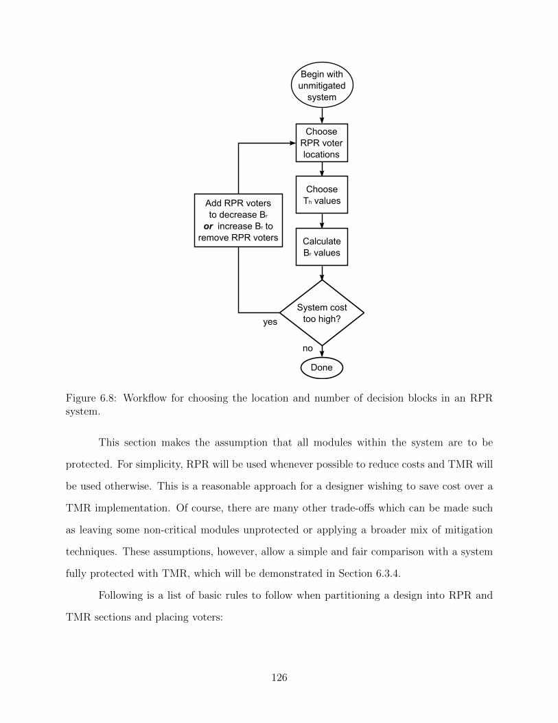
Figure 6.8: Workflow for choosing the location and number of decision blocks in an RPRsystem.
This section makes the assumption that all modules within the system are to be
protected. For simplicity, RPR will be used whenever possible to reduce costs and TMR will
be used otherwise. This is a reasonable approach for a designer wishing to save cost over a
TMR implementation. Of course, there are many other trade-offs which can be made such
as leaving some non-critical modules unprotected or applying a broader mix of mitigation
techniques. These assumptions, however, allow a simple and fair comparison with a system
fully protected with TMR, which will be demonstrated in Section 6.3.4.
Following is a list of basic rules to follow when partitioning a design into RPR and
TMR sections and placing voters:
126
1. A voter should be inserted in every feedback loop: either a TMR voter or an RPR
voter.
2. A voter must be inserted before changing from RPR to TMR or from mitigated to
unmitigated.
3. Non-arithmetic modules must be protected with TMR.
4. Small modules with feedback should be protected with TMR due to the large cost of
RPR voters.
5. RPR voters, which are large, should be used sparingly.
6. Both RPR and TMR voters should be triplicated for maximum reliability.
Each of these points will be explained individually in the following paragraphs.
A voter should be inserted in every feedback loop
Some method must be used to synchronize the data within the three loop replicas in
the event of an SEU corruption. The simplest way to do this is to cut the path of every
feedback loop with a voter. When an SEU causes an error in a of the feedback loops, the data
in that loop remains corrupted even after scrubbing repairs the SEU. The circuit, at that
point, must either be reset or the loop can be resynchronized with the other two functioning
loops with a voter in the feedback loop [44], [45].
A voter must be inserted before changing from RPR to TMR
Changing from RPR to non-RPR mitigation (or to unmitigated) requires the insertion
of an RPR voter. As explained in Section 6.3.1, an RPR voter is required to decode the
three RPR outputs into a generally-usable signal. This applies when moving from a section
of the circuit protected with RPR to a section protected by TMR, as well. TMR requires
three identical inputs, so the differing outputs of RPR must be resolved into a single output
that is then read by three TMR modules, or directly into three identical outputs.
127

A voter is not needed when moving from TMR to RPR. In this case, one of the
TMR outputs is taken as the full-precision input and the two other TMR outputs are simply
truncated to the precision needed by the two reduced-precision modules. Similarly, moving
from unmitigated to RPR is accomplished by the three RPR modules tapping off from the
same signal and no voter modules are required.
Non-arithmetic modules must be protected with TMR
As explained in Section 4.3, RPR is only suitable for protecting arithmetic modules.
There is no general method for creating reduced-precision state machines or other arbitrary
logic.4 Thus non-arithmetic modules must be left unprotected or another method such as
TMR can be used.
Small modules with feedback should be protected with TMR
Because of the high cost of RPR voters, it is undesirable to use them within small
feedback loops—those with a relatively small amount of hardware. For example, consider
the simple feedback circuit illustrated in Figure 6.9. The feedback loop should be cut by
a voter to keep the redundant circuit synchronized. In addition, if the register holds and
arithmetic value, an RPR implementation of the circuit might be considered. An RPR voter
for this module, however, would be the same size as that for a more complex module such as
a multiplier or filter with the same bit-widths. For this particular module, it would actually
be more efficient to apply full TMR to the circuit to make use of simple TMR voters rather
than to create an RPR version.
In this example, a simple circuit like this requires roughly 16 LUTs (for the multi-
plexer) and 16 FFs (for the register) in a Xilinx Virtex architecture. If the reduced-precision
replicas of this circuit use signals that are 4 bits wide, each requires 8 LUTs and 8 FFs.
4It is possible that suitable reduced-cost circuits could be designed which perform some type of estimatesimilar to RPR for certain systems, though such cases are beyond the scope of this work. Snodgrass presenteda theoretical discussion of the characteristics of possible candidates for an extension of RPR [5].
128
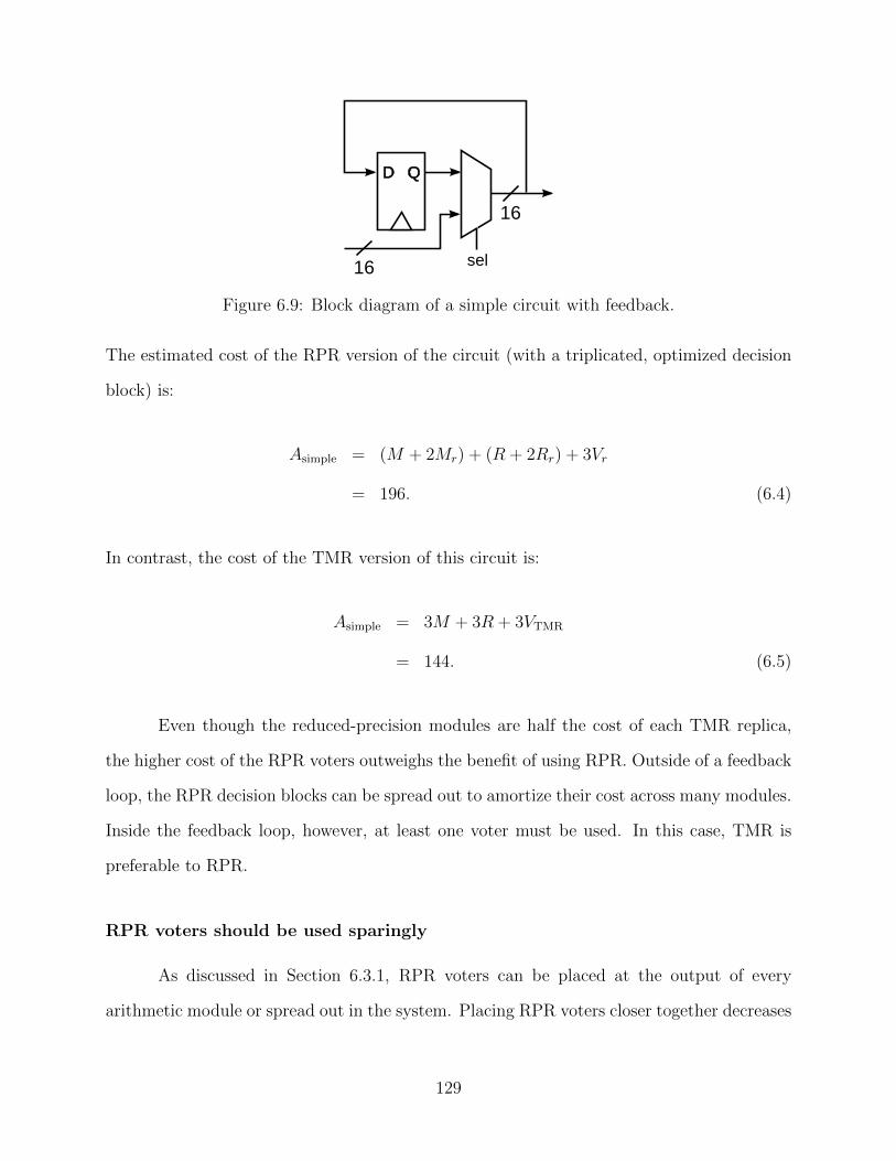
Figure 6.9: Block diagram of a simple circuit with feedback.
The estimated cost of the RPR version of the circuit (with a triplicated, optimized decision
block) is:
Asimple = (M + 2Mr) + (R + 2Rr) + 3Vr
= 196. (6.4)
In contrast, the cost of the TMR version of this circuit is:
Asimple = 3M + 3R + 3VTMR
= 144. (6.5)
Even though the reduced-precision modules are half the cost of each TMR replica,
the higher cost of the RPR voters outweighs the benefit of using RPR. Outside of a feedback
loop, the RPR decision blocks can be spread out to amortize their cost across many modules.
Inside the feedback loop, however, at least one voter must be used. In this case, TMR is
preferable to RPR.
RPR voters should be used sparingly
As discussed in Section 6.3.1, RPR voters can be placed at the output of every
arithmetic module or spread out in the system. Placing RPR voters closer together decreases
129

the estimation error at the input to the voters, but the cost of the voters can quickly outpace
the cost of TMR, as shown in the previous example. To achieve an area gain over TMR,
then, the number of RPR voters should be limited as much as possible while still achieving
the desired performance.
Both RPR and TMR voters should be triplicated
In an FPGA, RPR and TMR voters are implemented using the same configurable
logic as the modules to be protected. This means the voters themselves are susceptible to
SEUs. It has long been known, therefore, that TMR voters internal to the FPGA should be
triplicated [42], [44] for maximum reliability. The same is true for RPR voters. A single RPR
voter creates a single point of failure and triplicating the voter removes that vulnerability.
By triplicating the RPR voter, it is essentially protected completely using TMR.
By following these basic rules, a system can be partitioned into TMR and RPR
sections and the locations of voters chosen. Section 6.3.4 will use these rules to partition the
recursive binary PAM receiver from Section 3.6.
6.3.3 System Mitigation Design
When applying SEU mitigation to an entire system, it is clear that many issues
and options must be considered. Section 6.1 provided a method for setting the decision
threshold Th for an RPR decision block. Section 6.2 discussed the considerations for setting
the reduced-precision bit-width, Br, for an RPR module. Section 6.3 has presented important
issues for using RPR voters and for mixing RPR with TMR. This section presents a possible
workflow for designing a system using RPR with TMR.
Figure 6.10 shows this suggested workflow, which includes elements from the decision
block workflow shown in Figure 6.8. First, the rules of Section 6.3.2 should be applied
to choose which modules should be protected with RPR and which should be protected
130

Figure 6.10: Workflow for applying RPR+TMR to a digital system.
with TMR. The locations of TMR voters for synchronization should be straightforward to
identify by analyzing the feedback loops in the design. Then an initial placement of RPR
voters should be made again using the rules from Section 6.3.2. Initial Br values for any
RPR modules can then be selected as discussed in Section 6.2. Having set the Br values,
131

the Th values for each RPR voter can be determined mathematically or experimentally as
described in Section 6.1.
With this initial implementation of RPR, the Th values can be analyzed at their
respective locations in the system to determine if they are acceptable for the system in
question, as discussed in Section 6.2.1. If any of the Th values is too large, either more voters
should be added or Br should be increased in that section. Once an acceptable set of Th
values is found, the resulting noise bounds should be examined with respect to the system
requirements. If the noise bound is tighter than necessary, area overhead can be reduced by
either reducing the number of RPR voters in the system or by decreasing the Br values of
some of the RPR modules. This optimization loop can be repeated until a suitable, low cost
implementation is found.
The following section gives an example of a system that benefits from this type of
workflow. It will require the application of several of the rules and considerations presented
in the preceding sections. By using these techniques, a reliable system can be constructed
at a much lower cost than full TMR.
6.3.4 Recursive System Experiments
This section demonstrates the RPR technique on the recursive system described in
Section 3.6. This system is more complex that the simple feed-forward systems that RPR
was demonstrated on in Sections 4.7, 5.3, and 6.2.3. This system contains feedback loops,
non-arithmetic components, and sections with small feedback loops. As a larger system, the
question of the number of RPR voters to use is also more complicated.
Implementation Details
Figure 6.11 shows a diagram of the receiver system annotated with the type of mit-
igation applied to each component in the system. The locations of a TMR voter (for syn-
chronization) and an RPR decision block are also indicated.
132
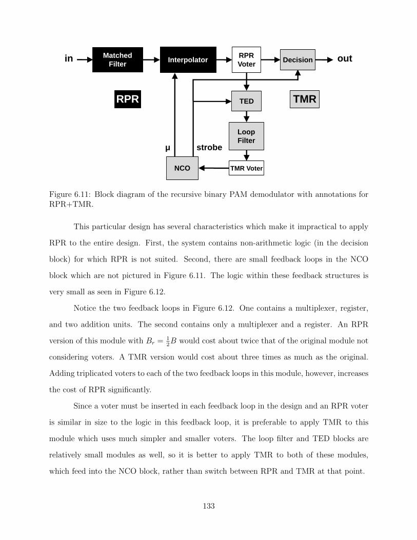
Figure 6.11: Block diagram of the recursive binary PAM demodulator with annotations forRPR+TMR.
This particular design has several characteristics which make it impractical to apply
RPR to the entire design. First, the system contains non-arithmetic logic (in the decision
block) for which RPR is not suited. Second, there are small feedback loops in the NCO
block which are not pictured in Figure 6.11. The logic within these feedback structures is
very small as seen in Figure 6.12.
Notice the two feedback loops in Figure 6.12. One contains a multiplexer, register,
and two addition units. The second contains only a multiplexer and a register. An RPR
version of this module with Br = 12B would cost about twice that of the original module not
considering voters. A TMR version would cost about three times as much as the original.
Adding triplicated voters to each of the two feedback loops in this module, however, increases
the cost of RPR significantly.
Since a voter must be inserted in each feedback loop in the design and an RPR voter
is similar in size to the logic in this feedback loop, it is preferable to apply TMR to this
module which uses much simpler and smaller voters. The loop filter and TED blocks are
relatively small modules as well, so it is better to apply TMR to both of these modules,
which feed into the NCO block, rather than switch between RPR and TMR at that point.
133

mu
2
strobe
1
zero
0
underflow
a
b
a>bz−1
one
1
add one
a
b
a + b
add
a
b
a + b
Scale
21
Register 3
d qz−1
Register 2
d qz−1
Register 1
d qz−1
Mux 2
sel
d0
d1
Mux 1
sel
d0
d1
1/N + LFout
a
b
a + b
1/N
0.5LFout
1
Figure 6.12: Block diagram of the NCO block within the recursive binary PAM demodulator,exported from Xilinx System Generator.
The matched filter and interpolator blocks, however, are ideal candidates for RPR.
Each contains a significant amount of arithmetic logic. The size of these blocks offsets the
cost of adding an RPR voter. In this case, we have chosen to place a single RPR voter at
the output of the interpolator. This means that the quantization error within the filter and
interpolator structures adds and requires a larger threshold for the RPR voter. Recall that a
larger threshold means that more SEU-induced noise passes through the system unnoticed.
The cost of the system is reduced, however, compared to an implementation with RPR voters
at the output of both the filter and the interpolator.
For the matched filter and interpolator blocks, reduced-precision modules with Br =
7 bits of precision at their inputs were added. We determined experimentally that this
redundancy factor (k = 7) would be a suitable trade-off between mitigation cost and SEU
protection for this system. The value of Th = 0.35 was also chosen experimentally to avoid
FD events in the RPR decision block.
The “RPR Voter” at the output of the interpolator used three identical decision blocks
and converted the three interpolator output signals (one full-precision and two reduced-
precision) into three identical full-precision outputs. The three identical outputs were needed
by the triplicated TED and decision blocks which were protected with TMR. The TMR voter
at the output of the loop filter block intersects the two feedback loops pictured, correcting
any synchronization issues between the three branches.
134

Experimental Results
Tables 6.8 and 6.9 show the fault injection results for the recursive demodulator
system. The results are similar to those observed for the feed-forward systems examined.
Specifically, TMR again eliminated virtually all of the catastrophic SEUs, leaving only four
susceptible configuration bits. The TMR implementation was over three times as large as
the unmitigated system in terms of FPGA slices. The system with the combination of RPR
and TMR (RPR+TMR) reduced the number of catastrophic bits by over 97% while only
doubling the size of the design.
Note that the number of Class 3 and Class 4 SEUs is higher than the feed-forward
designs protected with a similar level of RPR. In this experiment, any TMR failures in
the triplicated RPR decision block were not removed from the SEU classification test, as
explained in Section 5.3.1. The location of the decision block within the feedback loop
made it difficult to identify those SEUs accurately. Thus some of the catastrophic SEUs are
expected to be a result of the imperfect application of TMR to the RPR decision block and
could be removed as described in Section D.3.
Table 6.9 summarizes the SNR losses for each design. Again, while TMR eliminates
any SNR loss, the RPR+TMR approach reduces the overall number of high-noise errors
significantly. Losses of more than 6 dB were reduced from 8.40% to 0.190% while losses of
more than 3 dB were reduced from 9.92% to 1.85%. Recall that these numbers include the
catastrophic SEUs, which cause infinite SNR loss.
Figure 6.13 shows the combined BER plot for the RPR+TMR implementation of the
receiver. This plot is similar to the unmitigated version of Figure 3.16, but most of the
catastrophic bits (including the histogram spikes at a BER of 0.5) have been eliminated.
These results confirm that RPR is a viable option for mitigating catastrophic SEUs
in a recursive communications system as well. Though TMR nearly perfectly protected the
system, the overhead cost was predictably near 200%. The RPR+TMR design was effective
135
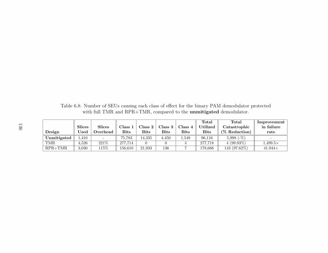
Table 6.8: Number of SEUs causing each class of effect for the binary PAM demodulator protectedwith full TMR and RPR+TMR, compared to the unmitigated demodulator.
Total Total ImprovementSlices Slices Class 1 Class 2 Class 3 Class 4 Utilized Catastrophic in failure
Design Used Overhead Bits Bits Bits Bits Bits (% Reduction) rate
Unmitigated 1,410 - 75,783 14,335 4,450 1,548 96,116 5,998 (-%) -TMR 4,526 221% 277,714 0 0 4 277,718 4 (99.93%) 1,499.5×RPR+TMR 3,030 115% 156,610 21,933 136 7 178,686 143 (97.62%) 41.944×
136

Table 6.9: Normalized percentage of SEUs causing certain SNR losses at BER of 10−5 forthe binary PAM demodulator protected with full TMR and RPR+TMR.
Design > 0.2 dB > 0.5 dB > 1 dB > 3 dB > 6 dB
Unmitigated 21.15% 15.19% 13.12% 9.92% 8.40%
TMR 0% 0% 0% 0% 2.08× 10⁻³%
RPR+TMR 22.97% 10.44% 6.86% 1.87% 0.19%
Figure 6.13: BER plot for the binary PAM receiver system with timing synchronizationusing RPR+TMR for mitigation.
at significantly reducing catastrophic SEUs, improving the failure rate of the system by 42×
at a cost about half that of TMR.
6.4 Summary
This chapter discussed many factors that are important when applying Threshold
RPR to a system. It showed that, for some systems, an error-detection threshold value T ∗h
lower than the maximum reduced-precision estimation error, εmax, could be found experimen-
tally which can increase the performance of an RPR system. This chapter also emphasized
the importance of the bit-with of the reduced-precision modules, Br, and demonstrated the
flexibility of RPR by varying this value. Finally, the chapter gave guidelines for the applica-
tion of RPR on complex, recursive systems and suggested a workflow for designing such an
RPR-based system.
137

138

CHAPTER 7. CONCLUSION
7.1 Summary of Contributions
The following is a summary of the research presented in this dissertation and its major
contributions:
Chapters 1 and 2 provided motivation for this research. These chapters gave the
background necessary to understand the importance and impact of mitigating SEUs on
FPGA systems and for reducing the cost of said mitigation. Chapter 2 explained current
techniques for mitigating SEUs and for evaluating the impact of SEUs on FPGA systems.
Chapter 3 went beyond previous SEU evaluation methods, focusing on FPGA-based
DSP and digital communications systems. That chapter presented a novel approach for
evaluating the SEU tolerance of these systems. While previous work treated all sensitive
upsets the same, this work showed that by analyzing the bit error rate caused by each
sensitive upset in a communications system, SEUs could be categorized into catastrophic
and non-catastrophic upsets.
Chapter 3 also introduced a novel fault injection platform that used this application-
specific method of evaluating an FPGA system. This platform allowed very rapid evaluation
of the communications systems in the presence of SEUs. With the new analysis method
and optimized fault injection platform, new mitigation approaches could be quickly and
comprehensively evaluated.
This new fault injection platform allowed for a detailed analysis of the locations of
critical and non-critical SEUs in a simple communications system. The critical SEUs in this
communications system were a small fraction of its sensitive SEUs and mainly made up the
139
global clock, global reset, and the most significant bits of arithmetic. This important result
lead to a search for reduced-cost mitigation techniques focusing on this critical subset of
SEUs in DSP circuits.
Using the knowledge gained from these fault injection experiments, Chapter 4 intro-
duced RPR as a possible alternative to TMR for DSP and communications systems. RPR
protects against the most critical SEUs in an arithmetic circuit by focusing mitigation on
the most significant bits of computation. Extensive fault injection experiments demonstrated
RPR to be an effective and efficient alternative to TMR. RPR required less than half the
overhead of TMR while providing good coverage of the most critical SEUs.
After determining RPR to be a valid alternative to TMR, Chapter 5 examined sev-
eral different approaches for applying RPR to a system. That chapter provided a description
and comparison of three different types of RPR, including Threshold RPR, Bounded RPR,
and RP-TMR. RP-TMR is a novel variation of RPR first presented in this dissertation and
was shown to have several desirable traits. Both Threshold and Bounded RPR were intro-
duced elsewhere but had not previously been compared directly. Fault injection experiments
demonstrated each type of RPR and Threshold RPR was determined to be the best technique
for FPGA-based systems.
As the superior implementation of RPR for FPGA systems, Threshold RPR was
examined further in Chapter 6. That chapter explained the effects of choosing reduced-
precision bit-widths and decision threshold and presented methods for determining good
values for each. A novel experimental approach for determining the error detection threshold
of RPR was presented that can significantly improve the performance of RPR in some systems
with no additional hardware cost.
Chapter 6 also included a demonstration of applying RPR to a more complex commu-
nications receiver. No previous work has used RPR to protect a complex system not entirely
suited to RPR. In examining this system, this dissertation identified several important steps
that should be taken to mitigate such a system using RPR and showed how RPR can be used
140
in conjunction with TMR. Fault injection experiments confirmed that a system protected
with a mixture of RPR and TMR had significantly improved reliability over the unmitigated
system at a much lower cost than TMR only.
Appendix F presents the design of a pair of on-orbit experiments to validate RPR as
a reduced-cost alternative to TMR. One design has already been deployed in orbit and the
other is scheduled to launch in 2011.
7.2 Future Work
This dissertation demonstrated how RPR could be applied to communications sys-
tems in order to reduce the cost of SEU mitigation on FPGAs. There is much that can still
be done to further investigate the properties and utility of RPR. Several examples of future
work are suggested here:
Application of RPR to new modules and applications
Although RPR was analyzed here specifically for DSP and communications systems,
it can be used in other types of systems that use arithmetic. It would be interesting to
examine other application domains and apply RPR in those systems. More types of DSP
systems could also be considered such as fast Fourier transform (FFT) modules, infinite
impulse response (IIR) filters, and trellis decoders.
Optimal placement of RPR decision blocks
Section 6.3.1 brought up the question of the optimal locations of RPR decision blocks
in large systems. This is an open question which is likely related to the optimal placement
of TMR voters, for which applicable research was cited in that section.
141
Automated tool to apply RPR
All of the example systems presented in this dissertation were created by hand. An
automated tool that could automatically apply RPR to an unmitigated system would be
extremely useful to an FPGA design engineer. This tool could be completely automatic,
determining the location of RPR voters and reduced-precision bit-widths, or could use input
from a designer to assist in these choices.
Extension of RPR with history-aided decision blocks
As presented here and in previous work, RPR decision blocks makes a cycle-by-cycle
comparison and decision. This can cause RPR to switch rapidly between the full-precision
and reduced-precision outputs. In some applications, this may not be desirable. By keeping
some history of previous decisions, RPR could be extended to switch over to reduced-precision
mode for an extended period of time rather than this cycle-by-cycle determination. In an
FPGA, for example, RPR could stay in reduced-precision mode until scrubbing has repaired
the configuration.
Use of variable thresholds
Threshold RPR need not have a static threshold in all systems. As mentioned, knowl-
edge of the input signal characteristics or operating environment can allow one to lower the
Th value. If these conditions are known to change, the performance of RPR may be improved
by using lower values of Th when the probability of false positive detections drop based on
these conditions.
Comparison of RPR with error-control coding
RPR in a communications system is designed to reduce the bit error rate of the
system in the presence of SEUs. This comes at a hardware cost. It would be interesting to
142

compare the cost and performance of RPR against data level redundancy techniques such
as error-control coding circuits in SEU environments.
7.3 Concluding Remarks
With FPGAs being used for DSP and communications applications in space systems,
SEU mitigation techniques for these systems are increasingly important. TMR offers good
protection, but comes at a high implementation cost. Application-specific mitigation tech-
niques such as RPR may be the future of SEU mitigation. These techniques can offer a
significant decrease in failure rate at a much lower cost than TMR.
This dissertation has provided significant insight into evaluating these alternative
mitigation techniques for FPGA systems. The application-specific evaluation technique pre-
sented for communications systems allows a superior evaluation of the effects of SEUs on the
systems and can be mimicked in other applications for similar results. With the knowledge
that catastrophic SEUs are a small fraction of the sensitive SEUs of some communications
systems, reduced-cost mitigation techniques such as RPR can provide significant advantages
to space-bound FPGA systems.
This dissertation has also showed that RPR is an excellent technique for protecting
DSP and communications systems, which rely heavily on arithmetic operations. With the de-
tailed comparison of different RPR techniques presented here, the strengths and weaknesses
of each are readily apparent. The examples given demonstrated that RPR is an effective
mitigation technique for FPGA systems and should be considered where cost of mitigation
is important. Even in a complex system in which RPR is unable to replace TMR completely,
RPR can be used jointly with TMR to significantly reduce costs.
Using the knowledge gained through this research, RPR could find its way aboard
future space systems. Knowing that most SEUs do not cause catastrophic errors in commu-
nications systems is key for evaluating the suitability of an FPGA design for such systems.
RPR, with its relatively low cost, could be used where TMR is prohibitively expensive.
143

This could allow new space systems to take advantage of the many benefits that commercial
FPGAs offer or could allow additional functionality to be added to systems by freeing up
valuable FPGA resources. RPR can open doors that the expensive TMR technique has
effectively shut.
144
ACRONYMS
ASIC application-specific integrated circuit. 1
BER see bit error rate. 29, 30
DSP digital signal processing. 1
DU see Detected upset. 57, 60, 160
DUT design under test. 19, 34
FD see False detection, no upset. 57, 60, 160
FPGA field-programmable gate array. 1
LSB least significant bit. 55
MSB most significant bit. 41, 55
MTTF see Mean time to failure. 24, 65, 160
NU see No upset, no false detection. 57, 60, 160
RPR reduced-precision redundancy. 51
SEU single event upset. 2, 8
SNR signal-to-noise ratio. 30
TMR triple modular redundancy. 12, 15, 23
UU see Undetected upset. 57, 60, 160
145

146

GLOSSARY OF TERMS
a The detection probability, a, is the fraction of upsets which are detected by the particular
RPR implementation. 57, 77
B The bit-width of the full-precision module in an RPR system. 62, 117
Br The bit-width of the reduced-precision module in an RPR system. 62, 103, 113
εe The error signal formed by the difference of the outputs of the full-precision and reduced-
precision modules in an RPR system. This can be considered the quantization noise
or the estimation error of the reduced-precision module: εe = FPtrue − RPout. 58,
59, 89, 90, 104, 147, 157, 168
εmax The absolute maximum value of the estimation error, εe: εmax = max |εe|. 59, 89, 104
εRPR The error signal at the output of an RPR system: εRPR = FPtrue − RPRout. 52, 89
ERPR-avg The average error bound of an RPR system, taking into account the probability
of each RPR upset case and the error bounds in each case. 104
εu The error signal formed by the difference of the outputs of the true full-precision output
in the absence of upsets and the actual full-precision module in an RPR system. This
is the SEU-induced noise signal for a particular upset: εu = FPtrue − FPout. 59, 157,
158, 164, 165, 168
FPout The output signal of the full-precision module in an RPR system. 51
FPtrue The output signal of the full-precision module in an RPR system in the absence of
soft errors. 52
Pfp The probability of a false positive detection event in any given clock cycle. 58
147
Pupset The probability of a soft error in the full-precision module of an RPR system in any
given clock cycle. 57
RPout The output signal of the reduced-precision module in an RPR system. 51
RPRout The output signal of an RPR system. 52
Th The error-detection threshold used by Threshold RPR. 75, 91, 103, 104, 115
T ∗h An alternate error-detection threshold used by Threshold RPR for which the value has
been lowered below the maximum estimation error: T ∗h < εmax. 107, 165
bit error rate A measure of the performance of a communications system. It is the number
of incorrectly-received bits in a signal divided by the total number of bits transferred.
145
catastrophic SEU An SEU which causes a highly detrimental effect on the DSP system
in question. Non-catastrophic SEUs may cause errors, but these errors are much less
significant than the catastrophic SEUs. 39, 43, 45
configuration scrubbing Any of several methods used to continually repair any SEUs in
the configuration memory of an FPGA. 13
detected upset An upset occurs in the full-precision module of an RPR system and is
detected. The RPR system enters the reduced-precision mode. 145
failure rate λ, the rate at which failures occur in time in a particular system [2]. 20, 21
false detection, no upset In an RPR system, though there is no upset in the full-precision
module, the RPR decision block indicates that there is an error. In this case, the RPR
system is incorrectly in reduced-precision mode. 145
full-precision degraded mode RPR operating mode in which the FP module is not op-
erating perfectly, but its output is still approximately equal to the reduced-precision
output, so the slightly-degraded FP output is used. 52, 57
148

full-precision perfect mode RPR operating mode in which there are no upsets in the FP
module and the output of the system is the correct full-precision output. 52, 57
mean time to failure The expected time from initial operation until a failure occurs. 145
no upset, no false detection In an RPR system, no upset exists in the full-precision mod-
ule and there is no false detection. The RPR system is in full-precision perfect mode.
145
reduced-precision mode RPR operating mode in which the FP module output is different
enough from the RP output to determine that there is an error in the FP module and
the RP output is used instead of the erroneous FP output. 52, 57
reliability The ability of a system or component to operate correctly for a specified period
of time. Reliability is often reported as a probability or as a function of time.. 15
sensitive The sensitive configuration bits are a subset of the utilized bits of an FPGA
design. When a sensitive bit is upset, the output of the design is altered for some
input or input sequence. 19, 20, 33, 34, 37, 43, 45, 64, 139, 149, 153, 164
sensitivity The number and location of the sensitive configuration bits of a particular
FPGA design. 19, 20, 151
SEU-induced noise The corruption of a digital signal due to an SEU in the FPGA con-
figuration. 30, 114, 158, 164
undetected upset An upset occurs in the full-precision module of an RPR system and is
not detected. The RPR system operates in full-precision degraded mode. 145
utilized bit A utilized configuration bit is a memory cell which the FPGA design in question
utilizes. For most FPGA designs, the majority of the available configuration cells are
unused. 19, 41, 64, 66, 68, 70, 149, 153, 154
149

150
REFERENCES
[1] P. Ostler, M. Caffrey, D. Gibelyou, P. Graham, K. Morgan, B. Pratt, H. Quinn, and
M. Wirthlin, “SRAM FPGA reliability analysis for harsh radiation environments,” Nu-
clear Science, IEEE Transactions on, vol. 56, no. 6, pp. 3519–3526, 2009.
[2] D. P. Siewiorek and R. S. Swarz, ”Reliable Computer Systems”. A K Peters, 1998.
[3] E. Johnson, M. J. Wirthlin, and M. Caffrey, “Single-event upset simulation on an
FPGA,” in Proceedings of the International Conference on Engineering of Reconfig-
urable Systems and Algorithms (ERSA), T. P. Plaks and P. M. Athanas, Eds. CSREA
Press, Jun. 2002, pp. 68–73.
[4] B. Shim, S. Sridhara, and N. Shanbhag, “Reliable low-power digital signal processing
via reduced precision redundancy,” Very Large Scale Integration (VLSI) Systems, IEEE
Transactions on, vol. 12, no. 5, pp. 497–510, 2004.
[5] J. Snodgrass, “Low-Power fault tolerance for spacecraft FPGA-Based numerical com-
puting,” Ph.D. dissertation, Naval Postgraduate School, Monterey, CA, Sep. 2006.
[6] O. Mencer, M. Morf, and M. Flynn, “PAM-Blox: High performance FPGA design for
adaptive computing,” in FPGAs for Custom Computing Machines, 1998. Proceedings.
IEEE Symposium on, Apr. 1998, pp. 167–174.
[7] M. Cummings and S. Haruyama, “FPGA in the software radio,” Communications Mag-
azine, IEEE, vol. 37, no. 2, pp. 108–112, Feb. 1999.
[8] R. Tessier and W. Burleson, “Reconfigurable computing for digital signal processing: A
survey,” The Journal of VLSI Signal Processing, vol. 28, pp. 7–27, 2001.
[9] M. Caffrey, “A space-based reconfigurable radio,” in Proceedings of the International
Conference on Engineering of Reconfigurable Systems and Algorithms (ERSA), T. P.
Plaks and P. M. Athanas, Eds. CSREA Press, Jun. 2002, pp. 49–53.
[10] P. Graham, M. Caffrey, M. Wirthlin, D. E. Johnson, and N. Rollins, “Reconfigurable
computing in space: From current technology to reconfigurable systems-on-a-chip,” in
151

Proceedings of the 2003 IEEE Aerospace Conference. Big Sky, MT: IEEE, Mar. 2003,
pp. T07 0603.1–12.
[11] G. R. Goslin, “A guide to using field programmable gate arrays (FPGAs) for application-
specific digital signal processing performance,” in Xilinx Application Notes. Xilinx
Corporation, 1995.
[12] R. Petersen and B. Hutchings, “An assessment of the suitability of FPGA-based systems
for use in digital signal processing,” in Field-Programmable Logic and Applications, 1995,
pp. 293–302.
[13] C. Dick and F. Harris, “Configurable logic for digital communications: Some signal
processing perspectives,” Communications Magazine, IEEE, vol. 37, no. 8, pp. 107–
111, Aug. 1999.
[14] M. Cummings and S. Haruyama, “FPGA in the software radio,” Communications Mag-
azine, IEEE, vol. 37, no. 2, pp. 108–112, Feb. 1999.
[15] B. Salefski and L. Caglar, “Re-configurable computing in wireless,” in Proceedings of
the 38th annual Design Automation Conference. Las Vegas, Nevada, United States:
ACM, 2001, pp. 178–183.
[16] B. L. Hutchings and B. E. Nelson, “GigaOp DSP on FPGA,” The Journal of VLSI
Signal Processing, vol. 36, no. 1, pp. 41–55, Jan. 2004.
[17] C. Dick, F. Harris, and M. Rice, “FPGA implementation of carrier synchronization for
QAM receivers,” The Journal of VLSI Signal Processing, vol. 36, no. 1, pp. 57–71, Jan.
2004.
[18] R. A. Mewaldt. Cosmic rays. California Institute of Technology. [Accessed 15-October-
2010]. [Online]. Available: http://www.srl.caltech.edu/personnel/dick/cos encyc.html
[19] C. Beth Barbier. (2008, Jan.) Cosmicopia. National Aeronautics and Space
Administration. [Accessed 15-October-2010]. [Online]. Available: http://helios.gsfc.
nasa.gov/
[20] N. Cohen, T. Sriram, N. Leland, D. Moyer, S. Butler, and R. Flatley, “Soft error consid-
erations for deep-submicron CMOS circuit applications,” in Electron Devices Meeting,
1999. IEDM Technical Digest. International, 1999, pp. 315–318.
152

[21] P. Hazucha and C. Svensson, “Impact of CMOS technology scaling on the atmospheric
neutron soft error rate,” Nuclear Science, IEEE Transactions on, vol. 47, no. 6, pp.
2586–2594, 2000.
[22] N. Seifert, X. Zhu, and L. Massengill, “Impact of scaling on soft-error rates in com-
mercial microprocessors,” Nuclear Science, IEEE Transactions on, vol. 49, no. 6, pp.
3100–3106, 2002.
[23] P. Dodd and L. Massengill, “Basic mechanisms and modeling of single-event upset in
digital microelectronics,” Nuclear Science, IEEE Transactions on, vol. 50, no. 3, pp.
583–602, Jun. 2003.
[24] C. Martha O’Bryan. (2009, Mar.) Radiation effects and analysis home page. National
Aeronautics and Space Administration Goddard Space Flight Center. [Accessed
15-October-2010]. [Online]. Available: http://radhome.gsfc.nasa.gov/
[25] D. E. Johnson, “Estimating the dynamic sensitive cross section of an FPGA design
through fault injection,” Master’s thesis, Brigham Young University, Provo, UT, Apr.
2005.
[26] H. Quinn, P. Graham, J. Krone, M. Caffrey, and S. Rezgui, “Radiation-induced multi-
bit upsets in SRAM-based FPGAs,” Nuclear Science, IEEE Transactions on, vol. 52,
no. 6, pp. 2455–2461, Dec. 2005.
[27] K. Chiba, I. Nashiyama, K. Sugimoto, N. Nemoto, H. Asai, Y. Iide, H. Shindo, N. Ikeda,
S. Kuboyama, and S. Matsuda, “Correlation between proton and heavy-ion SEUs in
commercial memory devices,” in Radiation Effects Data Workshop, 2003. IEEE, Jul.
2003, pp. 127–132.
[28] T. Karnik and P. Hazucha, “Characterization of soft errors caused by single event upsets
in CMOS processes,” Dependable and Secure Computing, IEEE Transactions on, vol. 1,
no. 2, pp. 128–143, Apr. 2004.
[29] R. Katz, K. LaBel, J. Wang, B. Cronquist, R. Koga, S. Penzin, and G. Swift, “Radiation
effects on current field programmable technologies,” Nuclear Science, IEEE Transac-
tions on, vol. 44, no. 6, pp. 1945–1956, Dec. 1997.
[30] S. Rezgui, “Radiation-tolerant ProASIC3 FPGAs radiation effects,” Actel Corporation,
Tech. Rep., Apr. 2010.
153
[31] M. Wirthlin, N. Rollins, M. Caffrey, and P. Graham, “Hardness by design techniques for
field-programmable gate arrays,” in Proceedings of the 11th Annual NASA Symposium
on VLSI design, Coeur d’Alene, ID, May 2003, pp. WA11.1–WA11.6.
[32] M. Bellato, P. Bernardi, D. Bortolato, A. Candelori, M. Ceschia, A. Paccagnella, M. Re-
baudengo, M. Sonza Reorda, M. Violante, and P. Zambolin, “Evaluating the effects of
SEUs affecting the configuration memory of an SRAM-based FPGA,” in DATE ’04:
Proceedings of the conference on Design, automation and test in Europe. Washington,
DC, USA: IEEE Computer Society, 2004.
[33] C. Carmichael, M. Caffrey, and A. Salazar, “Correcting single-event upsets through
Virtex partial configuration,” Xilinx Corporation, Tech. Rep., Jun. 1, 2000, xAPP216
(v1.0).
[34] M. Berg, C. Poivey, D. Petrick, D. Espinosa, A. Lesea, K. LaBel, M. Friendlich, H. Kim,
and A. Phan, “Effectiveness of internal versus external SEU scrubbing mitigation strate-
gies in a Xilinx FPGA: Design, test, and analysis,” Nuclear Science, IEEE Transactions
on, vol. 55, no. 4, pp. 2259–2266, Aug. 2008.
[35] K. Morgan, D. McMurtrey, B. Pratt, and M. Wirthlin, “A comparison of TMR with
alternative fault-tolerant design techniques for FPGAs,” Nuclear Science, IEEE Trans-
actions on, vol. 54, no. 6, pp. 2065–2072, 2007.
[36] Y. Hsu and E. Swartzlander, “Time redundant error correcting adders and multipli-
ers,” in Defect and Fault Tolerance in VLSI Systems. Proceedings of the 1992 IEEE
International Workshop on, 1992, pp. 247–256.
[37] W. Townsend, J. Abraham, and E. Swartzlander, “Quadruple time redundancy adders
[error correcting adder],” in Defect and Fault Tolerance in VLSI Systems, 2003. Pro-
ceedings. 18th IEEE International Symposium on, 2003, pp. 250–256.
[38] F. Lima, L. Carro, and R. Reis, “Designing fault tolerant systems into SRAM-based
FPGAs,” in Design Automation Conference, 2003. Proceedings, Jun. 2003, pp. 650–655.
[39] T. K. Moon, Error Correction Coding: Mathematical Methods and Algorithms. Wiley-
Interscience, 2005.
[40] R. Rochet, R. Leveugle, and G. Saucier, “Analysis and comparison of fault tolerant FSM
architecture based on SEC codes,” in Defect and Fault Tolerance in VLSI Systems, The
IEEE International Workshop on, Oct. 1993, pp. 9–16.
154

[41] J. von Neumann, “Probabilistic logics and the synthesis of reliable organisms from
unreliable components,” in Automata Studies. Princeton University Press, 1956, pp.
43–98.
[42] C. Carmichael, “Triple module redundancy design techniques for Virtex FPGAs,” Xilinx
Corporation, Tech. Rep., Nov. 1, 2001, xAPP197 (v1.0).
[43] C. Carmichael, E. Fuller, J. Fabula, and F. D. Lima, “Proton testing of SEU mitigation
methods for the Virtex FPGA,” in Proceedings of the IEEE Microelectronics Reliability
and Qualification Workshop, Pasadena, CA, Dec. 2001.
[44] N. Rollins, M. Wirthlin, M. Caffrey, and P. Graham, “Evaluating TMR techniques in the
presence of single event upsets,” in Proceedings Conference on Military and Aerospace
Programmable Logic Devices (MAPLD). Washington, D.C.: NASA Office of Logic
Design, AIAA, Sep. 2003, p. P63.
[45] J. M. Johnson and M. J. Wirthlin, “Voter insertion algorithms for FPGA designs using
triple modular redundancy,” in Proceedings of the 18th Annual ACM/SIGDA Interna-
tional Symposium on Field Programmable Gate Arrays. Monterey, California, USA:
ACM, 2010, pp. 249–258.
[46] A. Reddy and P. Banerjee, “Algorithm-based fault detection for signal processing ap-
plications,” Transactions on Computers, vol. 39, no. 10, pp. 1304–1308, Oct 1990.
[47] B. Shim and N. Shanbhag, “Energy-efficient soft error-tolerant digital signal processing,”
Very Large Scale Integration (VLSI) Systems, IEEE Transactions on, vol. 14, no. 4, pp.
336–348, 2006.
[48] P. Reyes, P. Reviriego, J. Maestro, and O. Ruano, “A new protection technique for finite
impulse response (FIR) filters in the presence of soft errors,” in Industrial Electronics,
IEEE International Symposium on, 2007, pp. 3328–3333.
[49] N. Shanbhag, K. Soumyanath, and S. Martin, “Reliable low-power design in the presence
of deep submicron noise,” in Low Power Electronics and Design. Proceedings of the 2000
International Symposium on, 2000, pp. 295–302.
[50] R. Hegde and N. Shanbhag, “Soft digital signal processing,” Very Large Scale Integration
(VLSI) Systems, IEEE Transactions on, vol. 9, no. 6, pp. 813–823, 2001.
[51] P. Reyes, P. Reviriego, J. Maestro, and O. Ruano, “New protection techniques against
SEUs for moving average filters in a radiation environment,” Nuclear Science, IEEE
Transactions on, vol. 54, no. 4, pp. 957–964, 2007.
155

[52] O. Ruano, P. Reyes, J. Maestro, L. Sterpone, and P. Reviriego, “An experimental
analysis of SEU sensitiveness on system knowledge-based hardening techniques,” in
Design and Diagnostics of Electronic Circuits and Systems, IEEE, 2007, pp. 1–6.
[53] P. Reviriego, J. Maestro, and O. Ruano, “Efficient protection techniques against SEUs
for adaptive filters: An echo canceller case study,” Nuclear Science, IEEE Transactions
on, vol. 55, no. 3, pp. 1700–1707, 2008.
[54] B. Shim and N. Shanbhag, “Reduced precision redundancy for low-power digital filter-
ing,” in Signals, Systems and Computers, Conference Record of the Thirty-Fifth Asilo-
mar Conference on, vol. 1, 2001, pp. 148–152.
[55] E. Fuller, M. Caffrey, P. Blain, C. Carmichael, N. Khalsa, and A. Salazar, “Radiation
test results of the Virtex FPGA and ZBT SRAM for space based reconfigurable comput-
ing,” in 2nd Annual Conference on Military and Aerospace Programmable Logic Devices
(MAPLD), Sep. 1999.
[56] C. Carmichael and C. W. Tseng, “Correcting single-event upsets in Virtex-4 FPGA
configuration memory,” Xilinx Corporation, Tech. Rep., Oct. 5, 2009, xAPP1088 (v1.0).
[57] K. Chapman, “SEU strategies for Virtex-5 devices,” Xilinx Corporation, Tech. Rep.,
Apr. 1, 2010, xAPP864 (v2.0).
[58] M. Alderighi, F. Casini, S. D’Angelo, M. Mancini, S. Pastore, and G. Sechi, “Evaluation
of single event upset mitigation schemes for SRAM based FPGAs using the FLIPPER
fault injection platform,” in Defect and Fault-Tolerance in VLSI Systems, 22nd IEEE
International Symposium on, Sep. 2007, pp. 105–113.
[59] B. Pratt, M. Wirthlin, M. Caffrey, P. Graham, and K. Morgan, “Noise impact of single-
event upsets on an FPGA-based digital filter,” in Field Programmable Logic and Appli-
cations, International Conference on, 2009, pp. 38–43.
[60] B. Pratt, M. Fuller, M. Rice, and M. Wirthlin, “Reliable communications using FPGAs
in high-radiation environments – Part I: Characterization,” in Communications (ICC),
2010 IEEE International Conference on, Cape Town, South Africa, May 2010.
[61] M. Violante, L. Sterpone, M. Ceschia, D. Bortolato, P. Bernardi, M. Reorda, and
A. Paccagnella, “Simulation-based analysis of SEU effects in SRAM-based FPGAs,”
Nuclear Science, IEEE Transactions on, vol. 51, no. 6, pp. 3354–3359, Dec. 2004.
[62] J. G. Proakis, Digital Communications, 4th ed. New York: McGraw-Hill, 2001.
156

[63] M. Rice, Digital Communications: A Discrete-Time Approach, 1st ed. New Jersey:
Pearson Prentice Hall, 2009.
[64] M. A. Sullivan, “Reduced precision redundancy applied to arithmetic operations in field
programmable gate arrays for satellite control and sensor systems,” Master’s thesis,
Naval Postgraduate School, Monterey, CA, Dec. 2008.
[65] A. Savich, M. Moussa, and S. Areibi, “The impact of arithmetic representation on
implementing MLP-BP on FPGAs: A study,” Neural Networks, IEEE Transactions on,
vol. 18, no. 1, pp. 240–252, Jan. 2007.
[66] B. Widrow and I. Kollar, Quantization Noise: Roundoff Error in Digital Computa-
tion, Signal Processing, Control, and Communications. Cambridge, UK: Cambridge
University Press, 2008.
[67] G. A. Constantinides and G. J. Woeginger, “The complexity of multiple wordlength
assignment,” Applied Mathematics Letters, vol. 15, no. 2, pp. 137–140, 2002.
[68] M.-A. Cantin, Y. Savaria, and P. Lavoie, “A comparison of automatic word length
optimization procedures,” in Circuits and Systems, IEEE International Symposium on,
vol. 2, 2002, pp. II–612–II–615.
[69] W. Osborne, R. Cheung, J. Coutinho, W. Luk, and O. Mencer, “Automatic accuracy-
guaranteed bit-width optimization for fixed and floating-point systems,” in Field Pro-
grammable Logic and Applications, International Conference on, Aug. 2007, pp. 617–
620.
[70] L. Sterpone, M. Violante, and S. Rezgui, “An analysis based on fault injection of hard-
ening techniques for sram-based fpgas,” Nuclear Science, IEEE Transactions on, vol. 53,
no. 4, pp. 2054–2059, Aug. 2006.
[71] L. Sterpone and M. Violante, “A new reliability-oriented place and route algorithm for
SRAM-based FPGAs,” Computers, IEEE Transactions on, vol. 55, no. 6, pp. 732–744,
Jun. 2006.
[72] B. Shim, “Error-tolerant digital signal processing,” Ph.D. dissertation, University of
Illinois at Urbana-Champaign, 2005.
[73] B. Pratt, M. Caffrey, P. Graham, E. Johnson, K. Morgan, and M. Wirthlin, “Improving
FPGA design robustness with partial TMR,” in Proceedings of the IRPS Conference,
Mar. 2006.
157
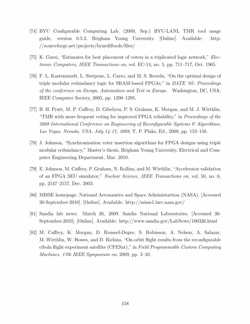
[74] BYU Configurable Computing Lab. (2009, Sep.) BYU-LANL TMR tool usage
guide, version 0.5.2. Brigham Young University. [Online]. Available: http:
//sourceforge.net/projects/byuediftools/files/
[75] K. Gurzi, “Estimates for best placement of voters in a triplicated logic network,” Elec-
tronic Computers, IEEE Transactions on, vol. EC-14, no. 5, pp. 711–717, Oct. 1965.
[76] F. L. Kastensmidt, L. Sterpone, L. Carro, and M. S. Reorda, “On the optimal design of
triple modular redundancy logic for SRAM-based FPGAs,” in DATE ’05: Proceedings
of the conference on Design, Automation and Test in Europe. Washington, DC, USA:
IEEE Computer Society, 2005, pp. 1290–1295.
[77] B. H. Pratt, M. P. Caffrey, D. Gibelyou, P. S. Graham, K. Morgan, and M. J. Wirthlin,
“TMR with more frequent voting for improved FPGA reliability,” in Proceedings of the
2008 International Conference on Engineering of Reconfigurable Systems & Algorithms,
Las Vegas, Nevada, USA, July 14-17, 2008, T. P. Plaks, Ed., 2008, pp. 153–158.
[78] J. Johnson, “Synchronization voter insertion algorithms for FPGA designs using triple
modular redundancy,” Master’s thesis, Brigham Young University, Electrical and Com-
puter Engineering Department, Mar. 2010.
[79] E. Johnson, M. Caffrey, P. Graham, N. Rollins, and M. Wirthlin, “Accelerator validation
of an FPGA SEU simulator,” Nuclear Science, IEEE Transactions on, vol. 50, no. 6,
pp. 2147–2157, Dec. 2003.
[80] MISSE homepage. National Aeronautics and Space Administartion (NASA). [Accessed
30-September-2010]. [Online]. Available: http://misse1.larc.nasa.gov/
[81] Sandia lab news: March 26, 2009. Sandia National Laboratories. [Accessed 30-
September-2010]. [Online]. Available: http://www.sandia.gov/LabNews/100326.html
[82] M. Caffrey, K. Morgan, D. Roussel-Dupre, S. Robinson, A. Nelson, A. Salazar,
M. Wirthlin, W. Howes, and D. Richins, “On-orbit flight results from the reconfigurable
cibola flight experiment satellite (CFESat),” in Field Programmable Custom Computing
Machines, 17th IEEE Symposium on, 2009, pp. 3–10.
158

APPENDIX A. FAULT INJECTION EXPERIMENT CONFIGURATION
The fault injection experiments presented in this dissertation were conducted using
an FPGA board designed by SEAKR Engineering for the Xilinx Radiation Test Consortium
(XRTC). The board contains two Xilinx Virtex-II Pro FPGAs (XC2VP70-FF1704-6) and
a daughter card with a Virtex-4 FPGA (XC4VSX55-FF1148-10). The first Virtex-II Pro
FPGA is the ConfigMon (configuration monitor) FPGA, which controls the overall test and
injects faults into the design under test (DUT) FPGA. The second Virtex-II Pro FPGA is
the FuncMon (functional monitor) which generates the inputs that drive the DUT FPGA
and receives and analyzes the DUT FPGA’s outputs. The Virtex-4 FPGA is the DUT FPGA
which contains the design to be tested. Figure A.1 shows a photograph of this board with
the three FPGAs labeled.
Figure A.2 is a simplified diagram showing the function of ConfigMon FPGA. This
FPGA was designed to interface with a host PC over a USB 2.0 connection. The host PC
instructed this FPGA which bits in the configuration to test and received and recorded the
test results. The fault injection of the DUT FPGA was otherwise completely controlled by
the hardware-based fault injection (HW FI) core over the SelectMAP interface (SMAP I/F).
The ConfigMon’s state machine also controlled the duration of each test by sending com-
mands to the FuncMon FPGA. The results of the test were then passed from the FuncMon
to the ConfigMon and then onto the host PC to be recorded.
A.1 Sensitivity Experiments
To measure the sensitivity of a design, the fault injection experiments followed the
general flow of [3] as described in Section 2.3.2. On the XRTC board experiments, the circuit
159
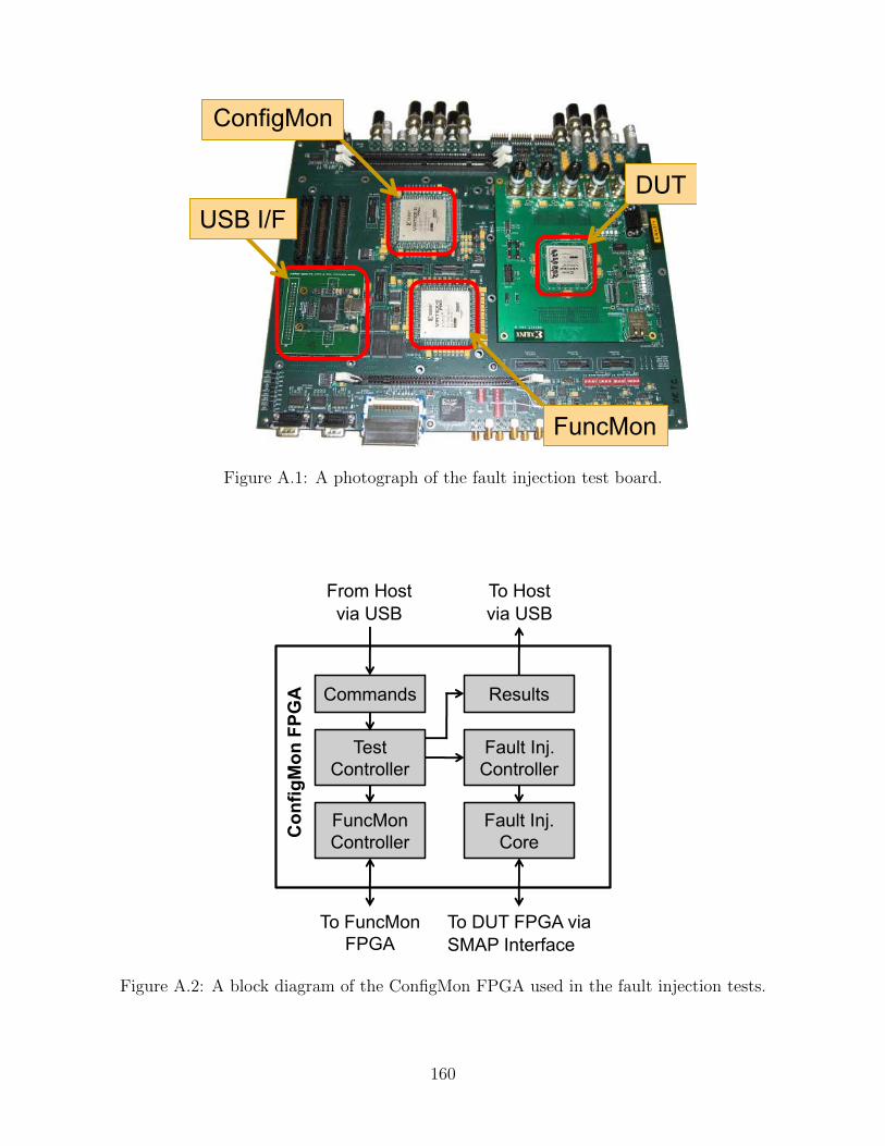
FuncMon
DUT
USB I/F
ConfigMon
Figure A.1: A photograph of the fault injection test board.
Figure A.2: A block diagram of the ConfigMon FPGA used in the fault injection tests.
160
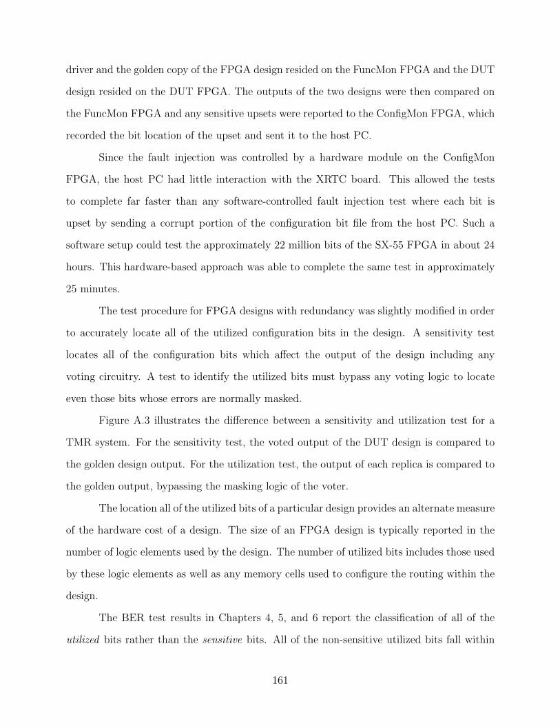
driver and the golden copy of the FPGA design resided on the FuncMon FPGA and the DUT
design resided on the DUT FPGA. The outputs of the two designs were then compared on
the FuncMon FPGA and any sensitive upsets were reported to the ConfigMon FPGA, which
recorded the bit location of the upset and sent it to the host PC.
Since the fault injection was controlled by a hardware module on the ConfigMon
FPGA, the host PC had little interaction with the XRTC board. This allowed the tests
to complete far faster than any software-controlled fault injection test where each bit is
upset by sending a corrupt portion of the configuration bit file from the host PC. Such a
software setup could test the approximately 22 million bits of the SX-55 FPGA in about 24
hours. This hardware-based approach was able to complete the same test in approximately
25 minutes.
The test procedure for FPGA designs with redundancy was slightly modified in order
to accurately locate all of the utilized configuration bits in the design. A sensitivity test
locates all of the configuration bits which affect the output of the design including any
voting circuitry. A test to identify the utilized bits must bypass any voting logic to locate
even those bits whose errors are normally masked.
Figure A.3 illustrates the difference between a sensitivity and utilization test for a
TMR system. For the sensitivity test, the voted output of the DUT design is compared to
the golden design output. For the utilization test, the output of each replica is compared to
the golden output, bypassing the masking logic of the voter.
The location all of the utilized bits of a particular design provides an alternate measure
of the hardware cost of a design. The size of an FPGA design is typically reported in the
number of logic elements used by the design. The number of utilized bits includes those used
by these logic elements as well as any memory cells used to configure the routing within the
design.
The BER test results in Chapters 4, 5, and 6 report the classification of all of the
utilized bits rather than the sensitive bits. All of the non-sensitive utilized bits fall within
161
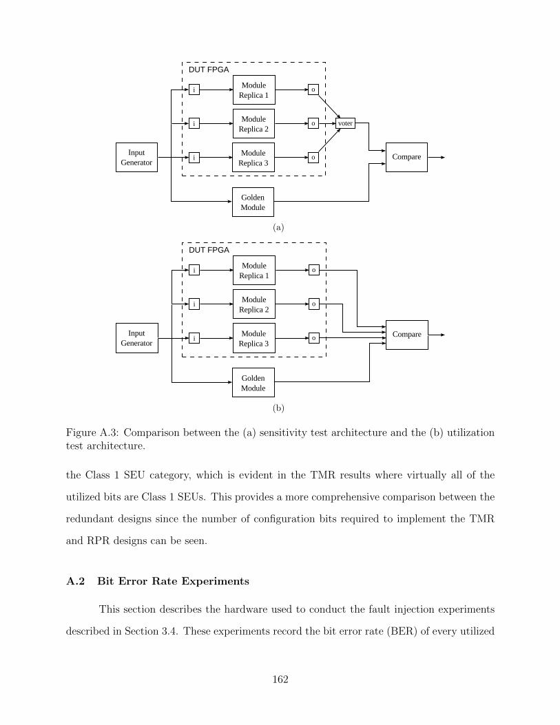
(a)
(b)
Figure A.3: Comparison between the (a) sensitivity test architecture and the (b) utilizationtest architecture.
the Class 1 SEU category, which is evident in the TMR results where virtually all of the
utilized bits are Class 1 SEUs. This provides a more comprehensive comparison between the
redundant designs since the number of configuration bits required to implement the TMR
and RPR designs can be seen.
A.2 Bit Error Rate Experiments
This section describes the hardware used to conduct the fault injection experiments
described in Section 3.4. These experiments record the bit error rate (BER) of every utilized
162
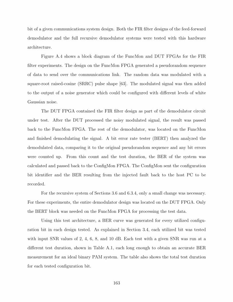
bit of a given communications system design. Both the FIR filter designs of the feed-forward
demodulator and the full recursive demodulator systems were tested with this hardware
architecture.
Figure A.4 shows a block diagram of the FuncMon and DUT FPGAs for the FIR
filter experiments. The design on the FuncMon FPGA generated a pseudorandom sequence
of data to send over the communications link. The random data was modulated with a
square-root raised-cosine (SRRC) pulse shape [63]. The modulated signal was then added
to the output of a noise generator which could be configured with different levels of white
Gaussian noise.
The DUT FPGA contained the FIR filter design as part of the demodulator circuit
under test. After the DUT processed the noisy modulated signal, the result was passed
back to the FuncMon FPGA. The rest of the demodulator, was located on the FuncMon
and finished demodulating the signal. A bit error rate tester (BERT) then analyzed the
demodulated data, comparing it to the original pseudorandom sequence and any bit errors
were counted up. From this count and the test duration, the BER of the system was
calculated and passed back to the ConfigMon FPGA. The ConfigMon sent the configuration
bit identifier and the BER resulting from the injected fault back to the host PC to be
recorded.
For the recursive system of Sections 3.6 and 6.3.4, only a small change was necessary.
For these experiments, the entire demodulator design was located on the DUT FPGA. Only
the BERT block was needed on the FuncMon FPGA for processing the test data.
Using this test architecture, a BER curve was generated for every utilized configu-
ration bit in each design tested. As explained in Section 3.4, each utilized bit was tested
with input SNR values of 2, 4, 6, 8, and 10 dB. Each test with a given SNR was run at a
different test duration, shown in Table A.1, each long enough to obtain an accurate BER
measurement for an ideal binary PAM system. The table also shows the total test duration
for each tested configuration bit.
163

Figure A.4: A block diagram of the BER fault injection test.
Table A.1: Fault injection run times for each SNR input value.
SNR (dB) Clock Cycles Data Symbols (bits)
2 40,000 10,0004 40,000 10,0006 400,000 100,0008 4,000,000 1,000,00010 40,000,000 10,000,000
Total 44,480,000 11,120,000
The full set of BER fault injection experiments collected and condensed a massive
amount of data. With approximately 3 million utilized bits tested throughout this disserta-
tion, over 33 trillion data bits were sent and processed on the XRTC board to produce the 3
million BER values reported in the tables and figures in this dissertation. This represented
a total of approximately 1,100 hours (about 45 days) of real time on the XRTC board.
164
APPENDIX B. SAMPLE NOISE DATA
This appendix contains sample data to illustrate some of the possible noise signals
for the designs presented in this dissertation. Section B.1 describes the estimation error,
εe, of several reduced-precision FIR filter designs. Section B.2 presents the probability mass
functions (pmf) of the SEU-induced noise, εu, for several SEUs affecting an FIR filter design.
Section B.3 presents some combined statistical measures of the εu signals for all sensitive
SEUs of the FIR filter design.
Although the data presented in this appendix cannot be assumed to be typical across
all designs, it is valuable as an example of the possible noise data. This data can help give
insight into the issues of mitigating SEU-induced noise and into improving techniques such
as RPR.
B.1 FIR Filter Estimation Error
Figures B.1–B.6 plot the probability mass function (pmf) of the estimation error, εe,
for a range of reduced-precision FIR filter designs. The full-precision filter design is the one
described in Section C.2 and shown in Figure C.1, with B = 15. The input signal had an
SNR of 8 dB in each case. The figures plot the pmf of the difference between the full- and
reduced-precision filter outputs for filters with Br = 2–7.
These figures show that εe for each of these reduced-precision designs have an approx-
imately Gaussian distribution. This fact is used in Section 6.1.3 to apply Threshold RPR to
this filter with a reasonable error-detection threshold, T ∗h , for which T ∗
h < εmax. These figures
also illustrate the reduction in the magnitude of the error signal as Br increases, reflecting
the fact that the approximation of the full-precision output improves as Br increases.
165
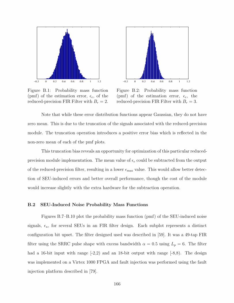
−0.2 0 0.2 0.4 0.6 0.8 1 1.2
Figure B.1: Probability mass function(pmf) of the estimation error, εe, of thereduced-precision FIR Filter with Br = 2.
−0.2 0 0.2 0.4 0.6 0.8 1 1.2
Figure B.2: Probability mass function(pmf) of the estimation error, εe, thereduced-precision FIR Filter with Br = 3.
Note that while these error distribution functions appear Gaussian, they do not have
zero mean. This is due to the truncation of the signals associated with the reduced-precision
module. The truncation operation introduces a positive error bias which is reflected in the
non-zero mean of each of the pmf plots.
This truncation bias reveals an opportunity for optimization of this particular reduced-
precision module implementation. The mean value of εe could be subtracted from the output
of the reduced-precision filter, resulting in a lower εmax value. This would allow better detec-
tion of SEU-induced errors and better overall performance, though the cost of the module
would increase slightly with the extra hardware for the subtraction operation.
B.2 SEU-Induced Noise Probability Mass Functions
Figures B.7–B.10 plot the probability mass function (pmf) of the SEU-induced noise
signals, εu, for several SEUs in an FIR filter design. Each subplot represents a distinct
configuration bit upset. The filter designed used was described in [59]. It was a 49-tap FIR
filter using the SRRC pulse shape with excess bandwidth α = 0.5 using Lp = 6. The filter
had a 16-bit input with range [-2,2) and an 18-bit output with range [-8,8). The design
was implemented on a Virtex 1000 FPGA and fault injection was performed using the fault
injection platform described in [79].
166
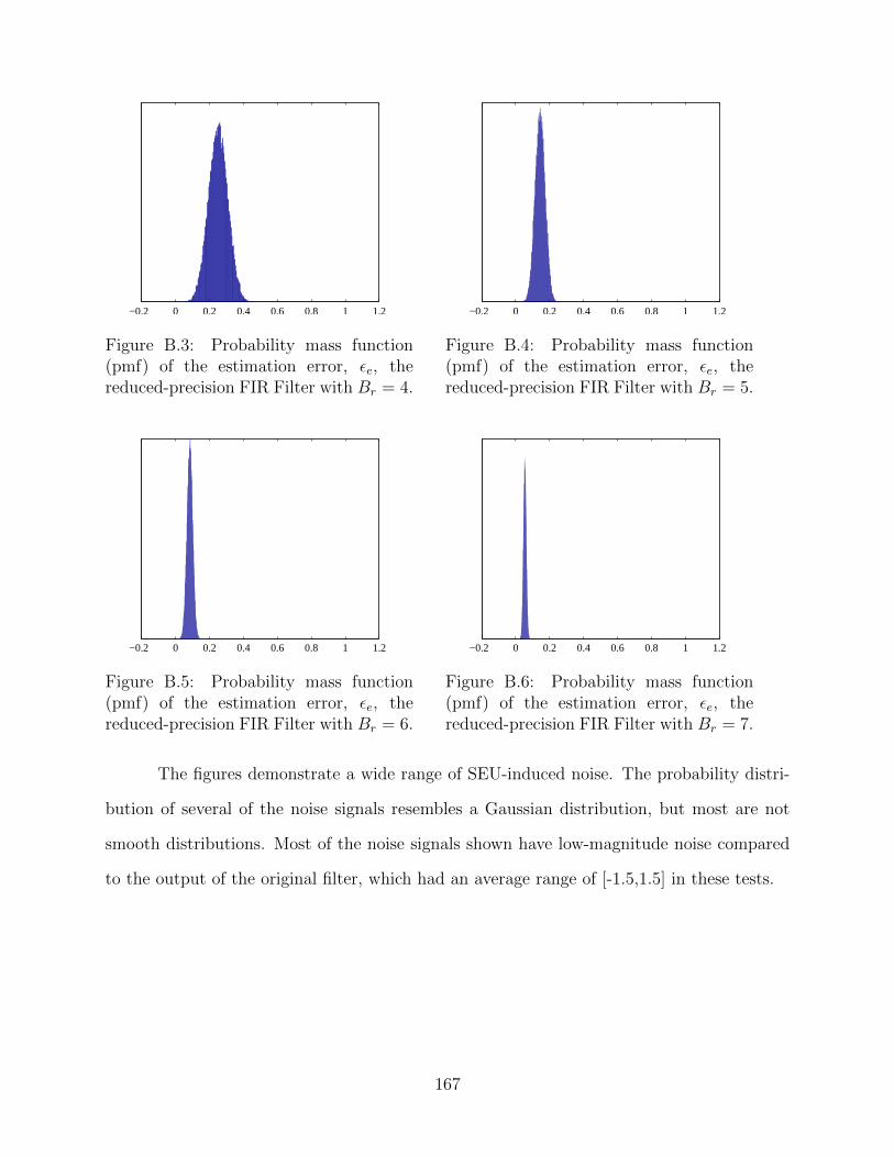
−0.2 0 0.2 0.4 0.6 0.8 1 1.2
Figure B.3: Probability mass function(pmf) of the estimation error, εe, thereduced-precision FIR Filter with Br = 4.
−0.2 0 0.2 0.4 0.6 0.8 1 1.2
Figure B.4: Probability mass function(pmf) of the estimation error, εe, thereduced-precision FIR Filter with Br = 5.
−0.2 0 0.2 0.4 0.6 0.8 1 1.2
Figure B.5: Probability mass function(pmf) of the estimation error, εe, thereduced-precision FIR Filter with Br = 6.
−0.2 0 0.2 0.4 0.6 0.8 1 1.2
Figure B.6: Probability mass function(pmf) of the estimation error, εe, thereduced-precision FIR Filter with Br = 7.
The figures demonstrate a wide range of SEU-induced noise. The probability distri-
bution of several of the noise signals resembles a Gaussian distribution, but most are not
smooth distributions. Most of the noise signals shown have low-magnitude noise compared
to the output of the original filter, which had an average range of [-1.5,1.5] in these tests.
167
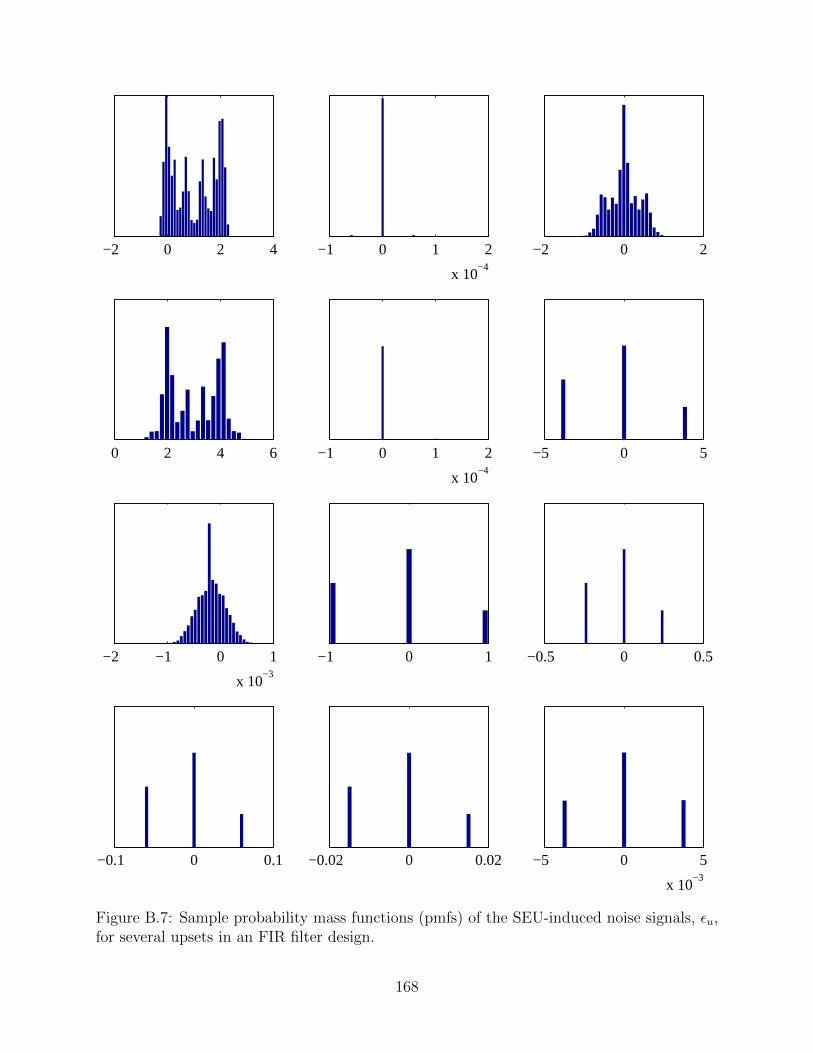
−1 0 1 2
x 10−4
−2 0 2
0 2 4 6 −1 0 1 2
x 10−4
−5 0 5
−2 −1 0 1
x 10−3
−1 0 1 −0.5 0 0.5
−0.1 0 0.1 −0.02 0 0.02 −5 0 5
x 10−3
−2 0 2 4
Figure B.7: Sample probability mass functions (pmfs) of the SEU-induced noise signals, εu,for several upsets in an FIR filter design.
168
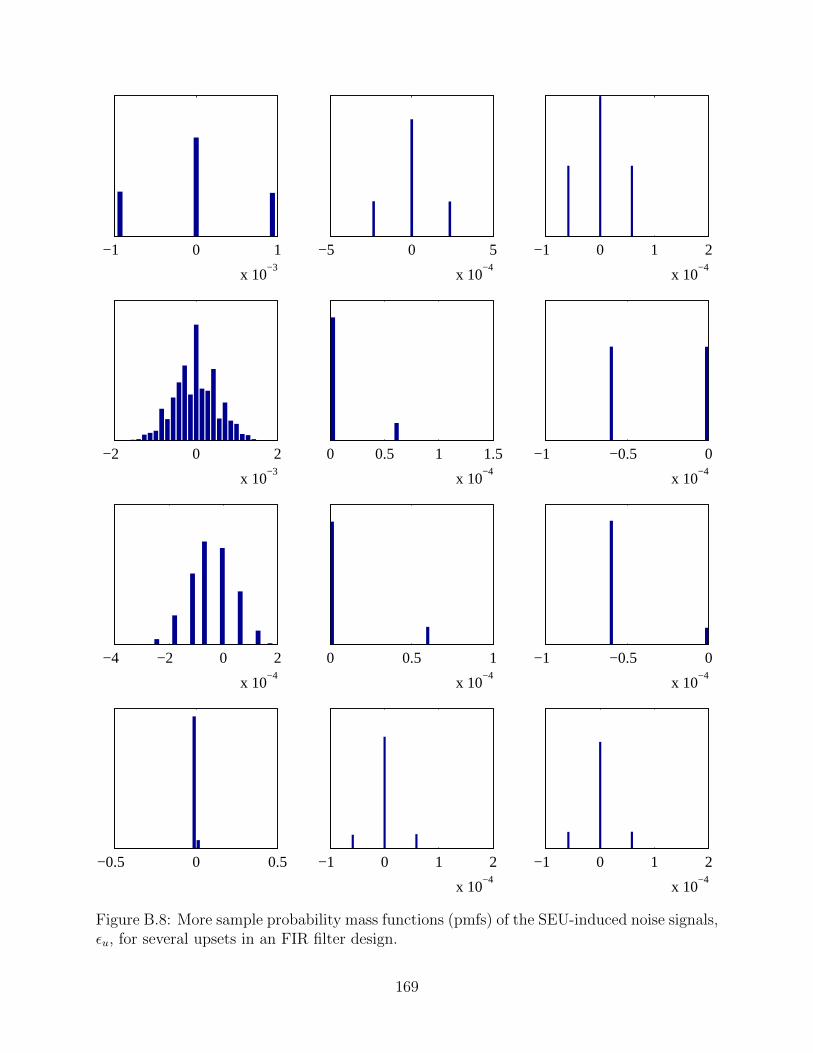
−5 0 5
x 10−4
−1 0 1 2
x 10−4
−2 0 2
x 10−3
0 0.5 1 1.5
x 10−4
−1 −0.5 0
x 10−4
−4 −2 0 2
x 10−4
0 0.5 1
x 10−4
−1 −0.5 0
x 10−4
−0.5 0 0.5 −1 0 1 2
x 10−4
−1 0 1 2
x 10−4
−1 0 1
x 10−3
Figure B.8: More sample probability mass functions (pmfs) of the SEU-induced noise signals,εu, for several upsets in an FIR filter design.
169
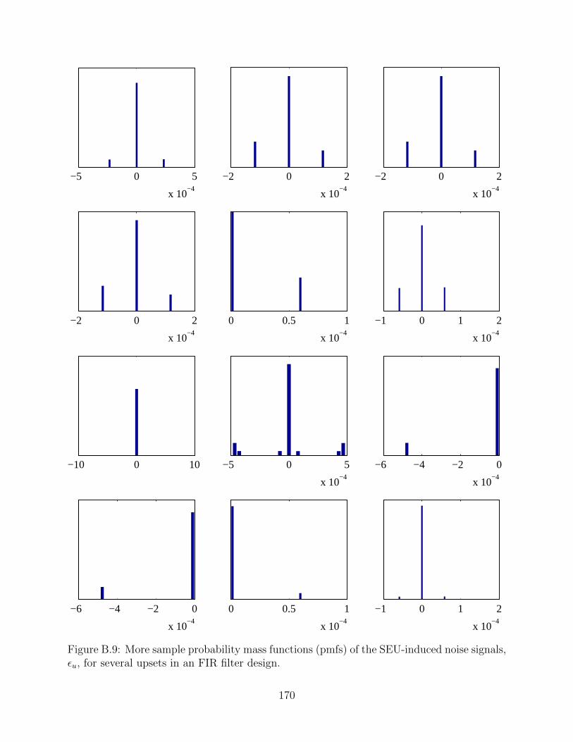
−2 0 2
x 10−4
−2 0 2
x 10−4
−2 0 2
x 10−4
0 0.5 1
x 10−4
−1 0 1 2
x 10−4
−10 0 10 −5 0 5
x 10−4
−6 −4 −2 0
x 10−4
−6 −4 −2 0
x 10−4
0 0.5 1
x 10−4
−1 0 1 2
x 10−4
−5 0 5
x 10−4
Figure B.9: More sample probability mass functions (pmfs) of the SEU-induced noise signals,εu, for several upsets in an FIR filter design.
170

−1 −0.5 0 −0.02 −0.01 0
−5 0 5
x 10−3
−0.2 −0.1 0 −0.2 −0.1 0
−4 −2 0
x 10−3
−1 −0.5 0
x 10−3
−0.01 −0.005 0
−0.01 0 0.01 −4 −2 0
x 10−4
−4 −2 0
x 10−3
−1 −0.5 0
Figure B.10: More sample probability mass functions (pmfs) of the SEU-induced noise sig-nals, εu, for several upsets in an FIR filter design.
171

B.3 SEU-Induced Noise Statistics
Figures B.11–B.16 show the combined statistics of the SEU-induced noise signals, εu,
for an FIR filter design. The filter design is the same as that in Section B.1. The histograms
in each figure include the statistics of the noise signal, εu, induced by every sensitive bit in
the filter design.
Figure B.11 plots a histogram of the mean value of all εu signals. Figure B.12 shows
more detail of this histogram. The sample mean of the noise signal was calculated:
µ =1
N
n∑1
x. (B.1)
Notice that the vast majority of SEUs have a mean close to zero. Some SEUs, cause higher
means, which is to be expected for upsets which cause a stuck-at fault in a high order bit of
the output, for example.
Figure B.13 is a histogram of the variance of all εu signals. Figure B.14, again, shows
more detail of this histogram. The variance shown is the sample variance:
σ2 =1
N
n∑1
(x− µ)2. (B.2)
The variance of the noise signals are again, mostly close to zero.
Figure B.15 plots a histogram of the power (mean square) of all εu signals while
Figure B.16 shows more detail. The power of the noise signal is calculated as:
power =1
N
n∑1
x2. (B.3)
The power of the noise signals, which can be used to calculate the SNR of the SEU-induced
noise, is distributed similar to the variance. This is not surprising given the mean of most
of the signals is close to zero.
172
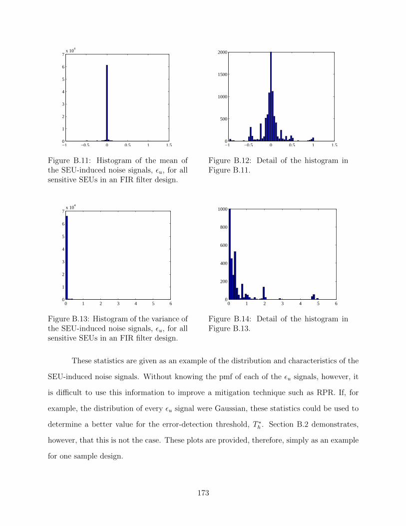
−1 −0.5 0 0.5 1 1.50
1
2
3
4
5
6
7x 10
4
Figure B.11: Histogram of the mean ofthe SEU-induced noise signals, εu, for allsensitive SEUs in an FIR filter design.
−1 −0.5 0 0.5 1 1.50
500
1000
1500
2000
Figure B.12: Detail of the histogram inFigure B.11.
0 1 2 3 4 5 60
1
2
3
4
5
6
7x 10
4
Figure B.13: Histogram of the variance ofthe SEU-induced noise signals, εu, for allsensitive SEUs in an FIR filter design.
0 1 2 3 4 5 60
200
400
600
800
1000
Figure B.14: Detail of the histogram inFigure B.13.
These statistics are given as an example of the distribution and characteristics of the
SEU-induced noise signals. Without knowing the pmf of each of the εu signals, however, it
is difficult to use this information to improve a mitigation technique such as RPR. If, for
example, the distribution of every εu signal were Gaussian, these statistics could be used to
determine a better value for the error-detection threshold, T ∗h . Section B.2 demonstrates,
however, that this is not the case. These plots are provided, therefore, simply as an example
for one sample design.
173
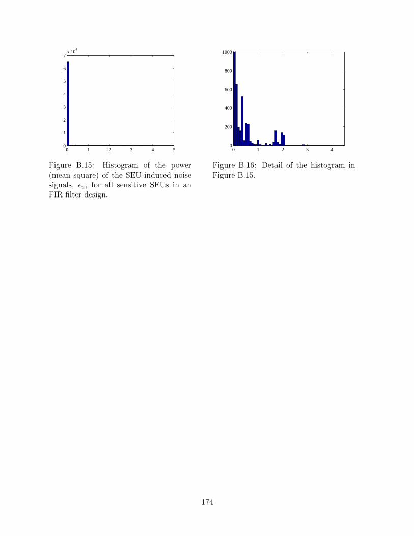
0 1 2 3 4 50
1
2
3
4
5
6
7x 10
4
Figure B.15: Histogram of the power(mean square) of the SEU-induced noisesignals, εu, for all sensitive SEUs in anFIR filter design.
0 1 2 3 40
200
400
600
800
1000
Figure B.16: Detail of the histogram inFigure B.15.
174
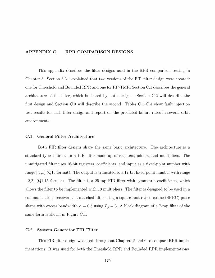
APPENDIX C. RPR COMPARISON DESIGNS
This appendix describes the filter designs used in the RPR comparison testing in
Chapter 5. Section 5.3.1 explained that two versions of the FIR filter design were created:
one for Threshold and Bounded RPR and one for RP-TMR. Section C.1 describes the general
architecture of the filter, which is shared by both designs. Section C.2 will describe the
first design and Section C.3 will describe the second. Tables C.1–C.4 show fault injection
test results for each filter design and report on the predicted failure rates in several orbit
environments.
C.1 General Filter Architecture
Both FIR filter designs share the same basic architecture. The architecture is a
standard type I direct form FIR filter made up of registers, adders, and multipliers. The
unmitigated filter uses 16-bit registers, coefficients, and input as a fixed-point number with
range [-1,1) (Q15 format). The output is truncated to a 17-bit fixed-point number with range
[-2,2) (Q1.15 format). The filter is a 25-tap FIR filter with symmetric coefficients, which
allows the filter to be implemented with 13 multipliers. The filter is designed to be used in a
communications receiver as a matched filter using a square-root raised-cosine (SRRC) pulse
shape with excess bandwidth α = 0.5 using Lp = 3. A block diagram of a 7-tap filter of the
same form is shown in Figure C.1.
C.2 System Generator FIR Filter
This FIR filter design was used throughout Chapters 5 and 6 to compare RPR imple-
mentations. It was used for both the Threshold RPR and Bounded RPR implementations.
175
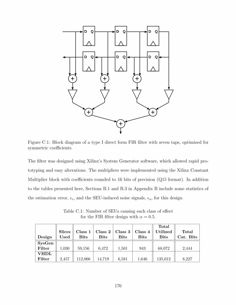
Figure C.1: Block diagram of a type I direct form FIR filter with seven taps, optimized forsymmetric coefficients.
The filter was designed using Xilinx’s System Generator software, which allowed rapid pro-
totyping and easy alterations. The multipliers were implemented using the Xilinx Constant
Multiplier block with coefficients rounded to 16 bits of precision (Q15 format). In addition
to the tables presented here, Sections B.1 and B.3 in Appendix B include some statistics of
the estimation error, εe, and the SEU-induced noise signals, εu, for this design.
Table C.1: Number of SEUs causing each class of effectfor the FIR filter design with α = 0.5.
TotalSlices Class 1 Class 2 Class 3 Class 4 Utilized Total
Design Used Bits Bits Bits Bits Bits Cat. Bits
SysGenFilter 1,030 59,156 6,472 1,501 943 68,072 2,444
VHDLFilter 2,457 112,066 14,719 6,581 1,646 135,012 8,227
176

Table C.2: Percentage of SEUs causing certain SNR losses at aBER of 10−5 for the FIR filter design with α = 0.5
Design > 0.2 dB > 0.5 dB > 1 dB > 3 dB > 6 dB
SysGen Filter 13.10% 10.57% 9.068% 6.289% 5.322%
VHDL Filter 17.00% 14.28% 12.86% 9.69% 8.140%
Table C.3: Sensitive failure rates (λ) for the FIR filter design in various orbits.
Design GEO GPS Molniya Polar LEO
SysGen Filter 1.04×10⁻⁵ 9.09×10⁻⁶ 9.90×10⁻⁶ 2.40×10⁻⁶ 6.48×10⁻⁸
VHDL Filter 2.06×10⁻⁵ 1.80×10⁻⁵ 1.96×10⁻⁵ 4.76×10⁻⁶ 1.29×10⁻⁷
Table C.4: Catastrophic failure rates (λ) for the FIR filter design in various orbits.
Design GEO GPS Molniya Polar LEO
SysGen Filter 3.73×10⁻⁷ 3.26×10⁻⁷ 3.55×10⁻⁷ 8.63×10⁻⁸ 2.33×10⁻⁹
VHDL Filter 1.25×10⁻⁶ 1.10×10⁻⁶ 1.20×10⁻⁶ 2.90×10⁻⁷ 7.83×10⁻⁹
C.3 VHDL FIR Filter
This FIR filter design was used in Chapter 5 for the RP-TMR implementation. In
order to create a correct RP-TMR implementation, this filter was designed structurally in
VHDL and EDIF (electronic design interchange format). This was done in order to ensure
that the correct low-level components were targeted as described in Section 5.1.3. To help
simplify this task, the multipliers in the RP-TMR filter are two-input multipliers with a
constant as one of the inputs. The custom multipliers created also may not be optimized
for the Xilinx architecture used for our testing. For these reasons, the filter used in the
RP-TMR tests is larger than that used in the Threshold and Bounded RPR tests.
177

178
APPENDIX D. RPR DECISION BLOCKS
This appendix contains supplemental material related to the decision blocks used with
RPR. Section D.1 calculates the area cost of the decision blocks associated with each variation
of RPR. Section D.2 estimates the cost of a simple design with different configurations of
the decision blocks. Section D.3 explains some of the difficulties seen in the fault injection
experiments when using triplicated RPR decision blocks.
D.1 Decision Block Area Costs
Section 5.2.1 presents a comparison of the relative costs of the decision blocks for each
variation of RPR. Figure 5.11 plotted the estimated area cost of each decision block as a
function of the reduced-precision bit-width, Br. This section supports the plot by estimating
the cost of each type of RPR decision block as a function of Br.
D.1.1 Threshold RPR Decision Block
This RPR decision block is fairly costly, especially on an FPGA. For comparison with
the other variations of RPR, we estimate the hardware cost of this decision block with an
n-bit full-precision input and two k-bit reduced-precision inputs. In a typical FPGA, most
functions of x input bits have the roughly the same cost due to their implementation in
lookup tables (LUTs). This is true for the adder, absolute value (abs), equality, comparison,
and multiplexer (mux) blocks shown in Figure 5.2. If we assign a cost of 1 for each LUT
utilized and each bit in an adder or other module consumes one LUT, the area cost of this
179
decision block is roughly:
Avoter = Aadder-n + Aabs-n + Acomparison-n + Amux-n + Aequality-k + AAND
= n+ n+ n+ n+ k + 1
= 4n+ k + 1. (D.1)
Table E.5 shows some actual implementation costs of this decision block on a Xilinx Virtex-4
FPGA, verifying this estimate.
The Threshold RPR decision block can be optimized under certain conditions. Shim
suggested a modification to the Threshold RPR decision block which is shown in Figure 5.3.
This circuit replaces the three upper modules in Figure 5.2. This optimization assumes that
the value chosen for Th is a power of two. With this assumption, the comparison block can
be implemented using simple AND and OR gates in place of a more complex n + 1 adder
block. The width m of the simplified comparator gates is dependent on the threshold value
chosen.
The area cost of this decision block is roughly1:
Avoter opt = Aadder-n + (AAND-m + AOR-m + AAND) + Amux-n + Aequality-k + AAND
= n+m
3+m
3+ 1 + n+ k + 1
= 2n+2
3m+ k + 1. (D.2)
Since the value of m must be smaller than n, this arrangement is less costly than the more
general decision block. Using a mid-range value of Th = 2−7, the necessary comparator width
is m = 8, Table E.6 confirms that this version is cheaper at a cost of just over one-half that
of the non-optimized version.
1This uses an approximate area cost of 13m for an m-bit logic function using the 4-input LUTs on a typical
FPGA, which is roughly the number of LUTs required.
180

D.1.2 Bounded RPR Decision Block
Using the same assumptions as in Section 5.1.1, the estimated cost of this Bounded
RPR decision block is roughly:
Avoter = 2 · Acomparison-n + Acomparison-k + AAND + ANOR + Aadder-k + Amux-n
= 2n+ k + 1 + 1 + k + n
= 3n+ 2k + 2. (D.3)
Table E.7 shows some actual implementation costs of this decision block on a Xilinx Virtex-4
FPGA. The estimate matches the table for larger values of k, but is pessimistic for smaller
values, where the FPGA synthesis software is able to optimize the blocks which compare
n-bit and k-bit signals. Even with the pessimistic estimate, however, the Bounded RPR
decision block cost estimate is lower than the Threshold RPR estimate for nearly all values
of n and k.
D.1.3 RP-TMR Decision Block
The decision blocks for RP-TMR are identical to the majority voters of TMR. These
voters are much smaller than the decision blocks required by Threshold and Bounded RPR.
Each bit of the voter takes three inputs and produces one output. In a typical FPGA
architecture, each of these three-input voters consumes one LUT resource. The cost of an
RP-TMR decision block, then, is roughly:
Avoter = Avoter-k
= k. (D.4)
Table E.8 shows some actual implementation costs of these voters on a Xilinx Virtex-4 FPGA
which verify this estimate. This cost is obviously much lower than those of the Threshold
181

and Bounded RPR decision blocks. If assuming k ≈ n/2, the decision blocks for Threshold
and Bounded RPR are 8–9 times larger, respectively, than the voters required for RP-TMR.
D.2 RPR Decision Block Placement
This section estimates the cost of several configurations of a 4-tap FIR filter, each
with a different arrangement of RPR decision blocks. Section 6.3 uses these calculations to
compare the efficiency of the different configurations. The 4-tap FIR filter circuit is shown
in Figure D.1.
For this system, RPR voters could be placed at the output of every multiplier in
addition to a voter at the final output. Assuming each reduced-precision multiplier needs to
be Br bits wide to achieve a specific threshold Th and each of reduced-precision adders is Br
bits wide as well, the total area cost of the system would be:
Afilter = 4 · (M + 2Mr) + 3 · (A+ 2Ar) + 4 · (R + 2Rr) + 5Vr, (D.5)
where M and Mr are the area costs of a full-precision and reduced-precision multiplier, A
and Ar are the costs of the adders, R and Rr are the costs of the registers, and Vr is the cost
of a voter.
In order to compare two implementations, we can use the resource utilization tables in
Appendix E. We will assign the costs of these variables the number of LUTs and/or flip-flops
in each module. If we set B = 16 and Br = 8, these values become: M = 127, Mr = 26,
A = 17, Ar = 9, R = 16, Rr = 8, and Vr = 44 (in the best case, using Shim’s optimized,
non-triplicated voters). With these estimates, the total cost of the system is roughly:
Afilter = 4 · (127 + 2 · 26) + 3 · (17 + 2 · 9) + 4 · (16 + 2 · 8) + 5 · 44
= 1, 169, (D.6)
182

Figure D.1: Block diagram of a 4-tap FIR filter.
or with triplicated voters:
Afilter = 4 · (127 + 2 · 26) + 3 · (17 + 2 · 9) + 4 · (16 + 2 · 8) + 3 · 5 · 44
= 1, 609. (D.7)
Alternatively, a single voter could be placed at the final output. Assuming the same
threshold is desired at the output of the filter, the bit-widths of the reduced-precision modules
must increase. This increases the cost of the reduced-precision components, but there is a
decrease in the cost of the RPR voters. Assuming the error at the output of each multiplier
adds to create the total error for the filter, that error is four times larger than for a single
multiplier. In order to maintain the same error level and thus the same threshold, m =
log2(4) = 2 extra bits of precision must be added to the reduced-precision modules:
Afilter = 4 · (M + 2Mr+2) + 3 · (A+ 2Ar+2) + 4 · (R + 2Rr+2) + Vr+2. (D.8)
183
The total cost of this version of the system is:
Afilter = 4 · (127 + 2 · 43) + 3 · (17 + 2 · 11) + 4 · (16 + 2 · 10) + 44
= 1, 157, (D.9)
or with triplicated voters:
Afilter = 4 · (127 + 2 · 43) + 3 · (17 + 2 · 11) + 4 · (16 + 2 · 10) + 3 · 44
= 1, 245. (D.10)
D.3 Triplicated Decision Blocks
In this dissertation, all of the fault injection tests involving RPR were conducted using
triplicated RPR decision blocks. Because the RPR decision block is implemented using the
same SEU-sensitive logic as the rest of the FPGA design, it is reasonable to protect them
somehow. The most straightforward protection method is to use TMR to eliminate all SEU
sensitivity.
In the fault injection tests, however, it became clear that the RPR decision blocks
were not fully protected by TMR. Some SEU sensitivity remained in each RPR experiment,
to varying degrees. Although the RPR decision block was triplicated in each case (essentially,
TMR was applied to that module), some SEUs caused upsets more than one of the replicas
and overcame the TMR protection. This can be seen in the results of Section 4.7, where
RPR left many catastrophic SEUs.
TMR has been shown to be imperfect in FPGAs in some instances, where a single
configuration bit affects signal routing in two of the three TMR domains [70]. Events in which
TMR is overcome by a single upset are called cross-domain errors or TMR failures. This
problem has also been shown to be correctable, in a large extent, using reliability-oriented
routing techniques [71].
184
These specialized routing techniques were not available at the time these experiments
were run. Therefore, the configuration bits of the triplicated RPR decision blocks were
ignored in the BER tests results presented in Chapter 5 and in Sections 6.1 and 6.2. Instead,
all of the decision block configuration bits were classified as Class 1 SEUs. This made the
comparisons of the performance of different RPR implementations more accurate, especially
when comparing the different bit-widths.
Section 6.3.4 presented fault injection results on the recursive receiver design. In the
RPR implementation, the RPR decision block was located within the feedback loop. This
made it difficult to separate the configuration bits of the triplicated decision block from the
rest of the design. The results presented in that section include any TMR failures within
the RPR decision block.
185

186
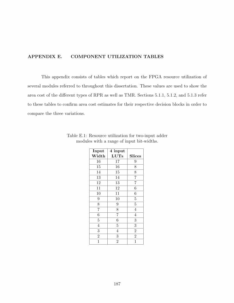
APPENDIX E. COMPONENT UTILIZATION TABLES
This appendix consists of tables which report on the FPGA resource utilization of
several modules referred to throughout this dissertation. These values are used to show the
area cost of the different types of RPR as well as TMR. Sections 5.1.1, 5.1.2, and 5.1.3 refer
to these tables to confirm area cost estimates for their respective decision blocks in order to
compare the three variations.
Table E.1: Resource utilization for two-input addermodules with a range of input bit-widths.
Input 4 inputWidth LUTs Slices
16 17 9
15 16 8
14 15 8
13 14 7
12 13 7
11 12 6
10 11 6
9 10 5
8 9 5
7 8 4
6 7 4
5 6 3
4 5 3
3 4 2
2 3 2
1 2 1
187
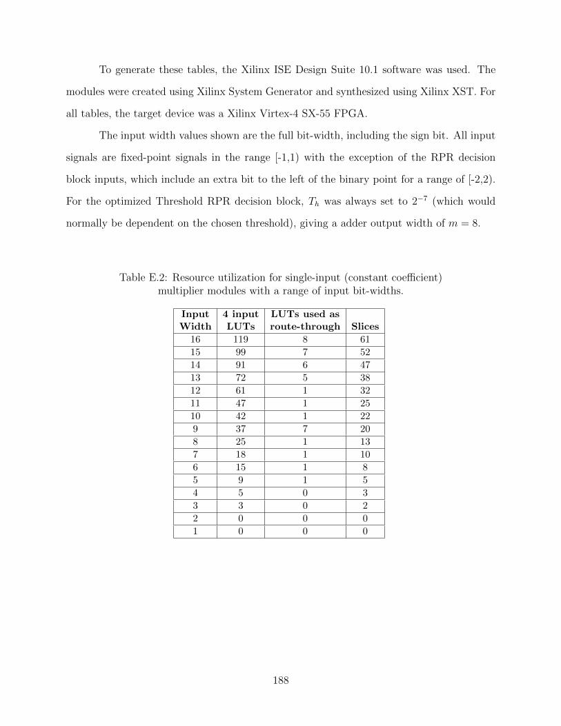
To generate these tables, the Xilinx ISE Design Suite 10.1 software was used. The
modules were created using Xilinx System Generator and synthesized using Xilinx XST. For
all tables, the target device was a Xilinx Virtex-4 SX-55 FPGA.
The input width values shown are the full bit-width, including the sign bit. All input
signals are fixed-point signals in the range [-1,1) with the exception of the RPR decision
block inputs, which include an extra bit to the left of the binary point for a range of [-2,2).
For the optimized Threshold RPR decision block, Th was always set to 2−7 (which would
normally be dependent on the chosen threshold), giving a adder output width of m = 8.
Table E.2: Resource utilization for single-input (constant coefficient)multiplier modules with a range of input bit-widths.
Input 4 input LUTs used asWidth LUTs route-through Slices
16 119 8 61
15 99 7 52
14 91 6 47
13 72 5 38
12 61 1 32
11 47 1 25
10 42 1 22
9 37 7 20
8 25 1 13
7 18 1 10
6 15 1 8
5 9 1 5
4 5 0 3
3 3 0 2
2 0 0 0
1 0 0 0
188
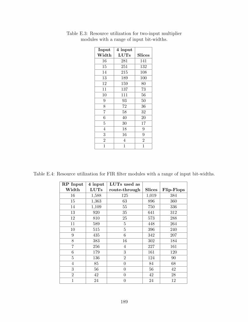
Table E.3: Resource utilization for two-input multipliermodules with a range of input bit-widths.
Input 4 inputWidth LUTs Slices
16 281 141
15 251 132
14 215 108
13 189 100
12 159 80
11 137 73
10 111 56
9 93 50
8 72 36
7 58 32
6 40 20
5 30 17
4 18 9
3 16 9
2 4 2
1 1 1
Table E.4: Resource utilization for FIR filter modules with a range of input bit-widths.
RP Input 4 input LUTs used asWidth LUTs route-through Slices Flip-Flops
16 1,588 125 1,019 384
15 1,363 63 896 360
14 1,109 55 750 336
13 920 35 641 312
12 810 25 573 288
11 589 5 448 264
10 515 5 396 240
9 435 6 342 207
8 383 16 302 184
7 256 4 227 161
6 179 3 161 120
5 136 2 124 90
4 85 0 84 68
3 56 0 56 42
2 42 0 42 28
1 24 0 24 12
189
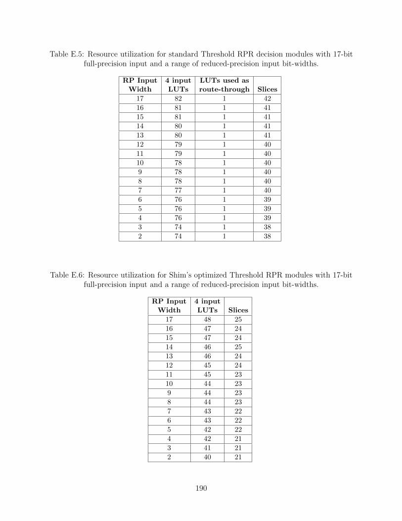
Table E.5: Resource utilization for standard Threshold RPR decision modules with 17-bitfull-precision input and a range of reduced-precision input bit-widths.
RP Input 4 input LUTs used asWidth LUTs route-through Slices
17 82 1 42
16 81 1 41
15 81 1 41
14 80 1 41
13 80 1 41
12 79 1 40
11 79 1 40
10 78 1 40
9 78 1 40
8 78 1 40
7 77 1 40
6 76 1 39
5 76 1 39
4 76 1 39
3 74 1 38
2 74 1 38
Table E.6: Resource utilization for Shim’s optimized Threshold RPR modules with 17-bitfull-precision input and a range of reduced-precision input bit-widths.
RP Input 4 inputWidth LUTs Slices
17 48 25
16 47 24
15 47 24
14 46 25
13 46 24
12 45 24
11 45 23
10 44 23
9 44 23
8 44 23
7 43 22
6 43 22
5 42 22
4 42 21
3 41 21
2 40 21
190
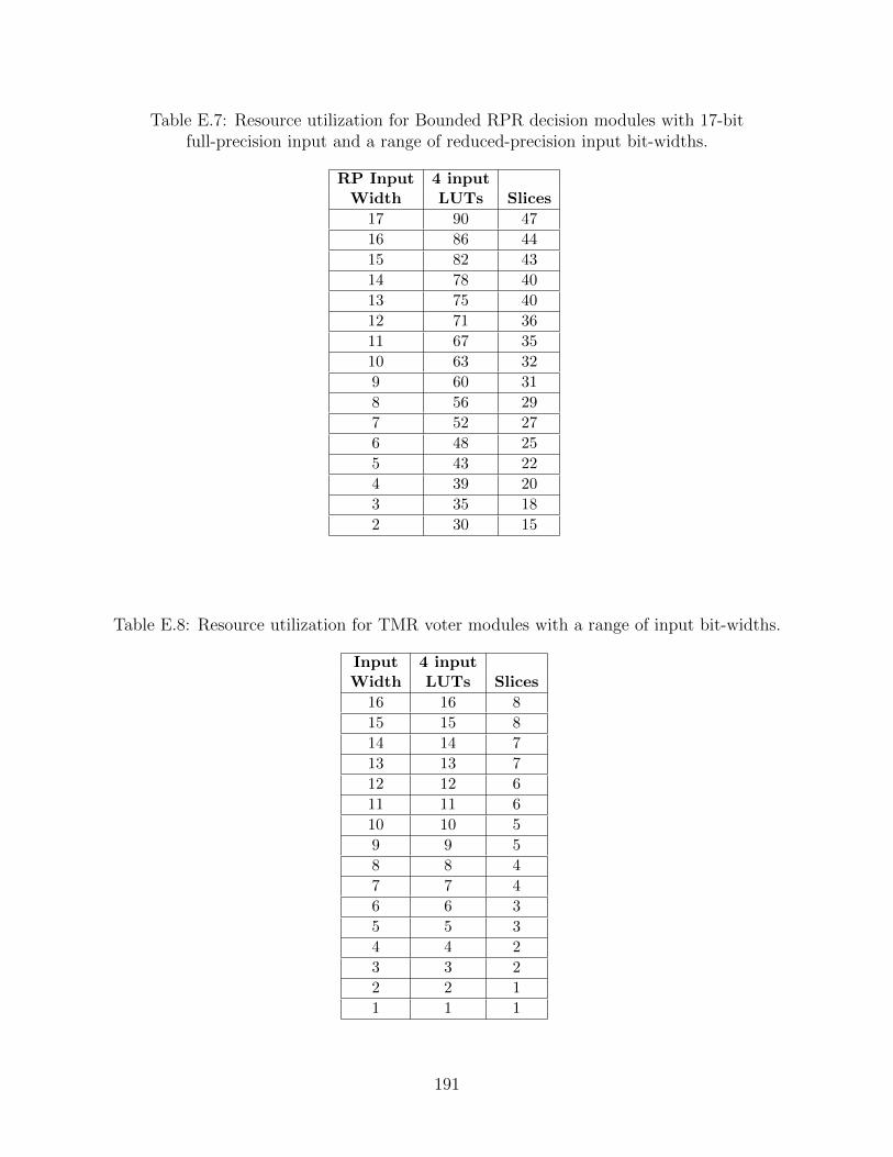
Table E.7: Resource utilization for Bounded RPR decision modules with 17-bitfull-precision input and a range of reduced-precision input bit-widths.
RP Input 4 inputWidth LUTs Slices
17 90 47
16 86 44
15 82 43
14 78 40
13 75 40
12 71 36
11 67 35
10 63 32
9 60 31
8 56 29
7 52 27
6 48 25
5 43 22
4 39 20
3 35 18
2 30 15
Table E.8: Resource utilization for TMR voter modules with a range of input bit-widths.
Input 4 inputWidth LUTs Slices
16 16 8
15 15 8
14 14 7
13 13 7
12 12 6
11 11 6
10 10 5
9 9 5
8 8 4
7 7 4
6 6 3
5 5 3
4 4 2
3 3 2
2 2 1
1 1 1
191

192
APPENDIX F. ON-ORBIT EXPERIMENTS
The goal of this dissertation was to analyze the effects of SEUs on FPGAs in radi-
ation environments and to present how to apply a mitigation technique with a lower cost
than the traditional TMR. Space was the primary radiation environment focused on in this
dissertation. As such, a pair of on-orbit experiments have been developed to further validate
the results presented in this dissertation.
Through collaborations with Sandia National Laboratory and Los Alamos National
Laboratory, we have gained access to two separate space-based FPGA platforms. These
platforms include an experimental payload to be placed on the International Space Station
(ISS) and an experimental satellite in low Earth orbit (LEO). This appendix describes these
platforms and the experiments developed to run on them.
F.1 MISSE-8 Experiment
The Materials International Space Station Experiment (MISSE) is a series of exper-
iments focused on testing the durability of various materials in the space environment [80].
Each MISSE payload has been mounted externally on the ISS for full exposure to the en-
vironment in low Earth orbit, where the space station resides. The 8th experiment in the
series, MISSE-8, includes the second SEU Xilinx-Sandia Experiment (SEUXSE II). This
experiment contains a Virtex-4 and a space-qualified Virtex-5 FPGA from Xilinx. SEUXSE
II is intended to allow researchers to analyze the effects of the harsh environment of space
on these FPGAs [81].
In collaboration with Sandia National Laboratory, we have developed a design to
be run on these FPGAs. This experiment was designed to verify the results presented in
193

Chapters 3 and 4. Figure F.1 shows a block diagram of the experiment. The Virtex-5 FPGA
is a radiation tolerant version and handles the data generation and analysis. The Virtex-4
FPGA is the design under test (DUT) chip and contains the receiver circuits being tested.
The DUT FPGA contains three unmitigated FIR filters along with one filter protected
with RPR. These were 25-tap FIR filters with symmetric coefficients using a square-root
raised-cosine (SRRC) pulse shape with excess bandwidth α = 0.5 using Lp = 3 and operating
at N = 4 samples/bit. The filters implemented were:
1. 16-bit logic-based FIR filter
2. 8-bit logic-based FIR filter
3. 16-bit DSP48-based FIR filter
4. 16-bit logic-based FIR filter, protected using Threshold RPR with Br = 7
The experiment was designed similarly to the fault injection experiment described
in Section 3.4. Each filter is fed a modulated, noisy signal. At the output of each filter, a
downsample and decision block complete the simple demodulator. The four demodulated
data streams are then passed through a bit error rate test (BERT) block to measure any
differences between the sent and received data streams. The control state machine watches
for any bit error rates above a pre-chosen threshold and records any such events.
This experiment is anticipated to confirm that very few SEUs will impact the bit
error rate of these demodulator systems. If enough data is collected, we expect that the
RPR filter system will perform better on average than the other implementations. Further,
we expect the relative frequency of high-BER events between the different filters to match
those reported in Sections 3.5.2 and 4.7.3.
As of this writing, there are no on-orbit results to report from this experiment.
MISSE-8 is currently scheduled to be delivered to ISS aboard the STS-134 Space Shuttle
mission in 2011.
194

Figure F.1: Block diagram of the experiment designed for the MISSE-8 experiment on theInternational Space Station.
F.2 CFE Experiment
The Cibola Flight Experiment Satellite (CFESat) was created by Los Alamos Na-
tional Laboratory to test the suitability of SRAM-based FPGAs for on-orbit processing.
The satellite launched in March 2007 and operates in the 560 km low Earth orbit. The
satellite receives approximately 2.4 SEUs per day. The processing payload of the satel-
lite includes three reconfigurable computing processor boards, each with three Virtex 1000
radiation-hardened XQVR1000 CG560 FPGAs [82].
Figure F.2 shows a block diagram of the experiment design for the CFE satellite. This
entire design is implemented on a single FPGA and the design is replicated across several of
the devices to increase the effective testing time. This experiment includes a data generator
similar to the MISSE-8 experiment, but no noise generator is included. The test architecture
allows for several demodulator with filters protected with RPR and a “golden” demodulator
protected with TMR.
195

During operation, the outputs of the RPR filter are compared against that of the
TMR filter. If any difference is detected by the control state machine, the output of the
faulty demodulator is selected with the mux. At that point, the squared difference between
the two filters is accumulated over a set number of clock cycles, N , which is later divided
by N to calculate the noise power between the two filters. This power measurement is then
recorded along with the bit error rate measured during this time period.
Figure F.2: Block diagram of the experiment designed for the Cibola Flight Experimentsatellite.
196

The initial results of the CFE RPR experiment are summarized in Table F.1. This
experiment is relatively power-intensive compared to others sharing operation time on CFE
and thus is not scheduled to run often. At the last report, the RPR test has operated for
49 FPGA device days, during which 140 configuration SEUs were detected. One of these
SEUs caused an error to propagate to the output of one of the RPR filters. This SEU did
not trigger the reduced-precision mode nor did it cause any bit errors in the binary PAM
receiver. Since the upset was seen at the output of the RPR voter and did not trigger the
reduced-precision mode, the event was a undetected upset (UU) event.
Table F.1: Results of the CFE RPR Test
FPGA Events With Events With Events WithOperation Config Total Events With Only TMR Only RPR TMR & RPR
Device Days SEUs Events No Bit Errors Bit Errors Bit Errors Bit Errors
49.0 140 1 1 0 0 0
It is anticipated that any updates to the CFE experimental data will be posted
on ScholarsArchive, BYU’s institutional repository for the scholarly and creative content
produced by the University. ScholarsArchive may be accessed online at:
http://lib.byu.edu/sites/scholarsarchive/.
197