analysis and control of excess leakage currents in nitride ... and control of excess leakage...
TRANSCRIPT

Instructions for use
Title Analysis and control of excess leakage currents in nitride-based Schottky diodes based on thin surface barrier model
Author(s) Kotani, Junji; Hashizume, Tamotsu; Hasegawa, Hideki
Citation Journal of Vacuum Science & Technology B: Microelectronics and Nanometer Structures, 22(4): 2179-2189
Issue Date 2004-08-20
Doc URL http://hdl.handle.net/2115/5803
Type article
File Information JVSTB22-4.pdf
Hokkaido University Collection of Scholarly and Academic Papers : HUSCAP
Analysis and control of excess leakage currents in nitride-based Schottkydiodes based on thin surface barrier model
Junji Kotani,a) Tamotsu Hashizume, and Hideki HasegawaResearch Center for Integrated Quantum Electronics (RCIQE) and Graduate School of Electronics andInformation Engineering, Hokkaido University, Sapporo 060-8628, Japan
~Received 18 January 2004; accepted 3 April 2004; published 20 August 2004!
Using a rigorous computer simulation program for current transport through a Schottky barrier withan arbitrary potential profile, the leakage current mechanism in GaN and AlGaN Schottky diodeswas investigated on the basis of the thin surface barrier~TSB! model recently proposed by theauthors’ group. Computer simulation assuming various possible defect density distributions wascarried out to reproduce the measured temperature dependent current voltage (I –V)-temperaturecharacteristics of the GaN and AlGaN Schottky diodes which showed excessive reverse leakage. Byassuming exponentially decaying distributions from surface for defect donors with energy depth of0.25 eV for GaN and 0.37 eV for Al0.15Ga0.85N, I –V curves measured by our group as well asreported in the literatures were almost completely reproduced both in forward and reverse directionover a wide temperature range. The defect donors are proposed to be N vacancies or their relatedcomplexes that are formed during metal deposition. The result confirms the validity of the TSBmodel. From the viewpoint of the TSB model, attempts were also made to suppress leakagecurrents. It was found that a low-energy electrochemical metal deposition process and a metal–insulator–semiconductor Schottky structure using an ultrathin Al2O3 film by electron cyclotronresonance oxidation of Al film were remarkably effective in reducing excess leakage currents due toreduction of defect deep donors. ©2004 American Vacuum Society.@DOI: 10.1116/1.1771678#
I. INTRODUCTION
Formation of high-quality Schottky barrier contacts onIII–V nitrides is essentially important for their application todevices such as high frequency/high power heterostructurefield effect transistors~HFETs!, metal–semiconductor FETs,power rectifiers, ultraviolet photodetectors, and various gassensors. In particular, smallness of reverse-bias leakage cur-rents of the Schottky barrier is a major concern in such de-vices from the viewpoints of precise depletion edge control,operation stability and reliability, power consumption, andnoise performance. However, Schottky diodes formed onGaN and AlGaN usually suffer from excess reverse leakagecurrents that are many orders of magnitude larger than theprediction of the thermionic emission~TE! model.1–8 Thiscauses serious problems such as the off-state leakage inFETs9 and the dark current in various kinds of detectors. Wehave also proposed recently that surface defects causinglarge leakage in Schottky gates are also responsible for theso-called current collapse in AlGaN/GaN HFETs.8
Although numerous studies have been made on GaN-based Schottky diodes having various kinds of barrier met-als, they focused, in most cases, on the forward current trans-port and only limited attempts have so far been made toexplain the mechanism for large reverse leakage currents.For example, Yuet al.10 and Miller et al.11 calculated tunnel-ing currents through GaN and AlGaN Schottky barriers, as-suming a triangular Schottky barrier. However, in their cal-culation, they had to use unreasonably large donor densities
that are more than 1 order of magnitude larger than the actualdoping concentration in order to reproduce the observed tem-perature~T!-dependent current–voltage (I –V) curves. Thus,they had to suggest some other processes such as defect-assisted tunneling which enhances leakage currents. Al-though several other groups also suggested contribution ofthe trap-assisted tunneling transport to excess reverse leak-age currents,3,12 such transport requires either a multisteptunneling process with unrealistically large electron capturecross sections of defects, or presence of a energy continuumformed by defects with a significantly wide energy bandwidth throughout the depletion region of the semiconductor.Thus, presence of such a transport process is far from havingbeen well established.
On the other hand, we have recently proposed an entirelydifferent model called the thin surface barrier~TSB! model7
for both forward and reverse current transport in GaNSchottky barriers. Here, it is assumed that the width of theSchottky barrier is reduced due to the presence of uninten-tional surface defect donors, and that thermionic field emis-sion ~TFE! or field emission~FE! through the resultant thinsurface barrier gives the major current leakage path in bothforward and reverse directions. This model could explain thetemperature dependences of the measuredI –V curves sys-tematically. However, detailed quantitative agreements be-tween theory and experiment were not entirely satisfactory,and this was thought to be due to use of approximate ana-lytical formulas that were obtainable only for the case of asimple rectangular distribution of shallow defect donors.
The purpose of this article is to further confirm the valid-ity of the TSB model for GaN and AlGaN Schottky barriers
a!Author to whom correspondence should be addressed; electronic mail:[email protected]
2179 2179J. Vac. Sci. Technol. B 22 „4…, Jul ÕAug 2004 1071-1023 Õ2004Õ22„4…Õ2179Õ11Õ$19.00 ©2004 American Vacuum Society

by a rigorous computer simulation. Limited attempts to re-duce excess leakage currents were also made on the basis ofan understanding. For this purpose, a simulation program foran arbitrary distribution of defect donors was developed. It isshown that deep defect donors with particular energy depthsand exponentially decaying density distributions from thesurface can reproduce the observedI –V characteristics ofour GaN and AlGaN Schottky diodes as well as others al-most completely over a wide temperature range. The defectdonors are proposed to be N vacancies or their related com-plexes that are formed during metal deposition. Additionally,a low-energy electrochemical metal deposition process and asurface passivation process using an ultrathin Al2O3 layerwere found to be very effective in suppressing formation ofsurface defect donors and reducing reverse leakage currents.
II. NUMERICAL SIMULATION METHOD OF I – V – TCHARACTERISTICS
A. Current transport in a Schottky barrier with anarbitrary potential profile
Let us start by considering current transport in a Schottkybarrier with an arbitrary potential barrier shown in Fig. 1 in ageneral way. The infinitesimal number of electrons having atotal energy,E in the infinitesimal volumedkxdkydkz in thek space may move from semiconductor to metal or frommetal to semiconductor through the Schottky barrier. Theseflows can be expressed by the following equations, respec-tively:
dns→m52 f s~E!@12 f m~E!#T~Ex!S 1
2p D 3
dkxdkydkz ,
~1a!
dnm→s52 f m~E!@12 f s~E!#T~Ex!S 1
2p D 3
dkxdkydkz .
~1b!
Here, it is assumed that energy and momentum are conservedduring transport and that the transport probability for an elec-tron is given byT(Ex) as a function of thex component ofenergy,Ex5\2kx
2/2m* wherekx is the wave number normal
to the barrier,\ is the reduced Planck’s constant, andm* isthe effective mass.ky andkz are the wave number parallel tothe Schottky barrier, andf s(E) and f m(E) are the Fermi–Dirac distribution functions for semiconductor and metal, re-spectively. Since only electrons that have a negative or posi-tive group velocity component can go into the Schottkybarrier from the semiconductor and from the metal side, re-spectively, and contribute to the current, the current fromsemiconductor to metal through the Schottky barrier regioncan be expressed by the following general expression:
J5E2`
` E2`
` E0
` 2q
\ S 1
2p D 3
@ f s~E!2 f m~E!#T~Ex!
3S dEx
dkxDdkxdkydkz . ~2!
By converting the double integral with respect toky andkz toan integral with respect to the parallel component energy,Ep5(\2/2m* )(ky
21kz2), Eq. ~2! reduces to
J54pqm*
h3 E0
`
T~Ex!E0
`
@ f s~Ep1Ex!
2 f m~Ep1Ex!#dEpdEx . ~3!
This is a very general basic expression for current transportin a Schottky barrier first derived for field emission intovacuum by Stratton.13 Presently it is often used in the devicesimulators. If we only consider electrons which have a suf-ficiently largex component energy to go over the Schottkybarrier, and we assume thatT(Ex)51 for them, ignoringpossible quantum reflection, and thatT(Ex)50 for the restof electrons, Eq.~3! reduces to the standard equation for TEtransport.
In the case where tunneling transport through the barrierbecomes very important as in the case of the present study,the simplest way to deal with it is to use the conventional~WKB! approximation, although a more elaborate and rigor-ous approach using the transition matrix may also be used.According to the Wentzel–Kramers–Brillouin approxima-tion, the tunneling probabilityT(Ex) for an electron havingan x component of energy,Ex , is given by
T~Ex!5expF22A2m*
\ Ex1
x2Af~x!2ExdxG , ~4!
where f (x) is the potential function, andx1 and x2 areclassical turning points shown in Fig. 1.
Historically, Padovani and Stratton14 studied the tunnelingcurrent transport through a Schottky barrier formed on ahighly doped material by combining Eqs.~3! and ~4!, andderived approximate analytical formulas forI –V character-istics. The background physics was the following. SinceT(Ex) is an exponentially increasing function ofEx as seenin Eq. ~4!, and f m(Ex) is an exponentially decreasing func-tion, the integrand in Eq.~3! forms a Gaussian peak for tun-neling at a certain energy whose energy position is tempera-ture dependent. At a sufficiently low temperature, this peaktakes place at the Fermi level, leading to the so-called FE at
FIG. 1. Schottky barrier with an arbitrary potential profile considered in thepresent simulation.
2180 Kotani, Hashizume, and Hasegawa: Analysis and control of excess leakage currents 2180
J. Vac. Sci. Technol. B, Vol. 22, No. 4, Jul ÕAug 2004
the Femi level. On the other hand, at elevated temperatures,the peak occurs above the Fermi level, leading to the TFE.From such a consideration, Padovani and Stratton were ableto derive approximate analytical formulas based on the Tay-lor expansion of the integrand of the above Eq.~3! aroundthe energy position for the Gaussian peak.
However, such an analytical treatment is only possible foruniformly doped semiconductors. Therfore, in the present ar-ticle, I –V characteristics were numerically calculated usingEqs. ~3! and ~4! for various possible distributions of near-surface defect donors on the basis of the TSB model. For thispurpose, a computer program to calculate Eqs.~3! and ~4!was developed. The potential profile of the Schottky barrierwas calculated by solving the Poisson equation self-consistently, using a simulation program previously devel-oped by our group. Unlike the analytical treatment by Pado-vani and Stratton,14 our numerical calculation includescontribution of thermionic emission by puttingT(Ex)51 forelectrons which can go over the Schottky barrier. Such a TEtransport becomes dominant at high temperatures. Thus, ourapproach takes into account all the possible current transportmechanisms automatically.
B. Comparison with previous analytical formulas andwith experiment on GaN
First, the validity of the previous analytical formulas byPadovani and Stratton14 was investigated for uniformlydoped semiconductors. For this, we calculatedI –V charac-teristics of a Schottky diode for various doping densities andtemperatures by our computer program, and compared theresults with those by the analytical formulas. For the forwardbias region, both methods gave nearly the sameI –V charac-teristics. In particular, analytical formulas included the fol-lowing well known formula for the ideality factornF for theforward TFE/TE transport
nF5~E00/kT!coth~E00/kT!, ~5a!
with
E0052q@ND/2e#1/2\/2~2m* !1/2, ~5b!
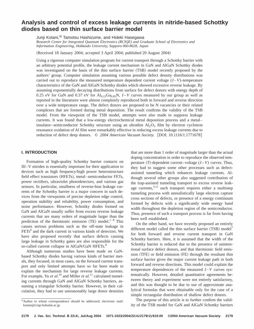
whereND is the bulk doping density of the semiconductor. InFig. 2~a!, calculated values ofnF using Eq.~5! are shown bysolid curves and those by our computer program are shownby symbols. The Schottky barrier height~SBH! was assumedto be 0.85 eV. A very good agreement is seen here.
For the reverse leakage currents, calculated curves by theanalytical formulas of Padovani and Stratton and those bythe computer program are shown in Fig. 2~b! by solid anddashed curves, respectively, for a Schottky diode with SBH50.85 eV and a doping density ofND5131017cm23.Again, good agreements are seen. Agreements became some-what poorer as the doping density was increased into the1018cm23 range due to the following unfavorable features ofthe analytical formulas for the reverse currents. Namely, twodifferent analytical formulas were derived: one for the largereverse bias range where transport is strongly by the FEmechanism and one for the small reverse bias range where
transport is strongly by the TFE mechanism. As a result, theerrors are enhanced in between two bias ranges, and an arti-ficial connection of two analytical formulas produce artificialkinks in the theoretical curves, as discussed in Ref. 7.
In spite of the above unfavorable features,I –V character-istics of highly doped Si and GaAs were reported to be wellexplained by the analytical formulas of Padovani andStratton.14 In order to see whether these formulas are alsoapplicable to Schottky barriers on highly doped GaN, reverseleakage currents data measured in our laboratory on aNi/n-GaN Schottky diode with a doping density ofND5131017cm23 is also shown in Fig. 2~b! by closed circles andsquares. It is seen in Fig. 2~b! that measured leakage currentsare many orders of magnitude larger than the theoretical val-ues calculated on the computer and by analytical formulas,and that the observed temperature dependence of current ismuch smaller than the theoretical prediction. Thus, a simpleTFE/FE transport model cannot explain large reverse leakagecurrents in GaN Schottky diodes at all.
FIG. 2. ~a! Theoretidal values of ideality factor, nF, of the forward current ofa Schottky diode with SBH50.85 eV as a function of temperature, calcu-lated using Eq.~5! ~solid lines!, and calculated by the present computerprogram~symbols!. ~b! TheoreticalI –V curves calculated by approximateanalytical formulas in Ref. 14~solid curves!, and by the present computerprogram~dashed curves! for a Schottky diode on uniformly dopedn-GaNwith ND5131017 cm23 and SBH50.85 eV. For comparison, measuredI –V data are shown by closed circles and squares for a Ni/GaN Schottkydiode withND5131017 cm23.
2181 Kotani, Hashizume, and Hasegawa: Analysis and control of excess leakage currents 2181
JVST B - Microelectronics and Nanometer Structures
C. TSB model
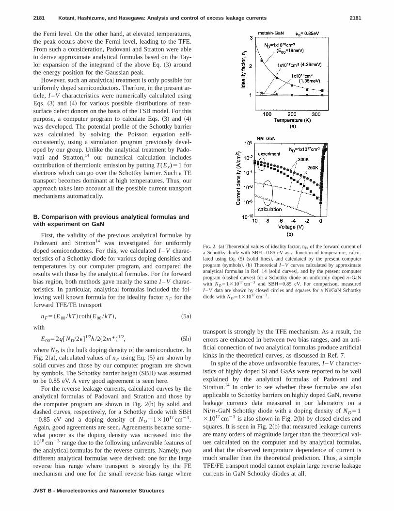
In order to explain anomalously large leakage currentsobserved in GaN and AlGaN Schottky diodes, Hasegawa andOyama7 have recently proposed a TSB model schematicallyshown in Fig. 3~a!. The model assumes formation of highdensities of unintentional defect donors near surface whichreduces the width of the Schottky barrier, thereby enhancingthe electron tunneling through the thin surface barrier in bothforward and reverse directions in the form of a Gaussianbeam. Either TFE or FE mechanism becomes dominant, de-pending on the temperature, bias direction, and bias magni-tude. Assuming a rectangular distribution of defect donors ontop of the uniform bulk doping, a set of analytical formulaswere derived, and they explained the behavior of anoma-lously large leakage currents remarkably well.7 However, de-tailed quantitative agreements between theory and experi-ment were not entirely satisfactory due to the use of a simplerectangular distribution for which only an analytical treat-ment was possible.
As for the origin of defect donors, we proposed in ourprevious article7 that the defect donor is due to N vacancy or
its related complex. Whether it is a shallow donor or deepdonor could not be decided by the previous calculation, sinceonly the case of the shallow donor could be treated analyti-cally. From the viewpoint of theoretical defect physics, Neu-gebauer and Van de Walle,15 and Boguslawskiet al.16 havecalculated energy levels of native point defects in GaN. Theyconcluded that a simple N vacancy defect (VN) acts as ashallow donor. On the other hand, recent results of calcula-tion by Yamaguchi and Junnarkar17 predicted that the VNdefect can form an s-like deep donor withEDD of about 0.3eV. Experimentally, our recent transient analysis of drain cur-rents in gateless HFETs with various surface treatments hasdetected presence of a N vacancy related deep donor level8
with the energy depth of 0.37 eV on the Al0.25Ga0.75N sur-face. Thus, if the calculation ofI –V curves can also be madefor various values of the energy depth of the defect donor, itwill be beneficial to resolve this issue.
Thus, theoreticalI –V curves were calculated in this ar-ticle for various possible distributions of the defect donor aswell as for various energy depths of the defect donor so as toreproduce the experimentalI –V curves over a wide tempera-ture range.
D. Parameters for numerical simulation of I – V – Tcurves
As possible spatial density distributions of the defect do-nor near surface, fittings were attempted for various peakedand decaying distributions shown in Fig. 3~b! with charac-teristic parameters. As peaked distributions, a rectangulardistribution, a parabola-shaped distribution, and a Gaussiandistribution were investigated, and as decaying distributionsfrom the surface, a linearly decaying distribution, a quadrati-cally decaying distribution, and an exponentially decayingdistribution were tried. Roughly speaking, if defects are in-troduced at a certain point of time during crystal growth, apeaked distribution is likely to occur, and if defects are in-troduced from the surface during crystal growth or duringprocessing after crystal growth, a decaying distribution fromthe surface is more likely. For the exponential distribution,the following expression was used:
Ndeep~x!5N0 exp~2x/l!. ~6!
As another important parameter, the energy depth,EDD ofthe defect donor shown in Fig. 3~c! was also varied as afitting parameter.
III. RESULT OF FITTING AND DISCUSSION
A. GaN and AlGaN Schottky diode samples
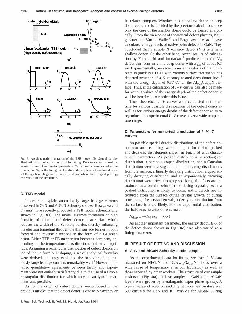
As the experimental data for fitting, we usedI –V datameasured on Ni/GaN and Ni/Al0.15Ga0.85N diodes over awide range of temperatureT in our laboratory as well asthose reported by other workers. The structure of our sampleis shown in Fig. 4~a!. In these samples,n-GaN andn-AlGaNlayers were grown by metalorganic vapor phase epitaxy. Atypical value of electron mobility at room temperature was500 cm2/V s for GaN and 100 cm2/V s for AlGaN. A ring
FIG. 3. ~a! Schematic illustration of the TSB model.~b! Spatial densitydistributions of defect donors used for fitting. Density shapes as well asvalues of their characteristic parameters,N0 , D and l were varied in thesimulation.ND is the background uniform doping level of shallow donors.~c! Energy band diagram for the defect donor where the energy depthEDD
was varied in the simulation.
2182 Kotani, Hashizume, and Hasegawa: Analysis and control of excess leakage currents 2182
J. Vac. Sci. Technol. B, Vol. 22, No. 4, Jul ÕAug 2004
shaped ohmic contact was formed by standard photolithog-raphy on the GaN and AlGaN surface, using a Ti/Al/Ti/Au~20/80/20/50 nm! alloy which was annealed at 600 °C for 2min. Circular Schottky electrodes with a radius ofr5100– 300mm were formed at the center of the ohmic ringby a conventional electron-beam~EB! deposition process.
Since our samples had a lateral electrode configuration forthe ohmic contact, there is a possibility that extra surfaceleakage currents flow in addition to bulk Schottky currents.To check the presence of such a possibility,I –V character-istics were measured for samples having different areas. Theresult for Ni/n-GaN Schottky diodes having different radii isshown in Fig. 4~b! in terms of the apparent current densitydefined as the measured current divided by the Schottkyelectrode area. The values of the apparent current densityagree very well among samples with different radii, indicat-ing that the measured apparent current densities can be re-garded as the true current densities representing bulkSchottky barrier currents.
B. Fitting for our GaN Schottky diodes
First, we tried to reproduce the experimental data of ourNi/n-GaN diode by calculatingI –V–T characteristics forvarious possible density distributions and various energydepths of the defect donor. It may look at first like variouscombinations of density functions, their parameters, and en-ergy depths will reproduce the experimental data due to the
presence of many fitting parameters. However, it has turnedout that it is not the case at all, and that successful fitting ispossible only for one particular combination of distributionand energy depth, i.e., an exponentially decaying distributionand an energy depth ofEDD50.25 eV, if one tries to repro-duce the experimental data in both forward and reverse di-rections over a wide temperature range at the same time.This is probably because of the extreme sensitive nature ofthe tunneling process against the change of distributionshapes and slight variation of parameter values.
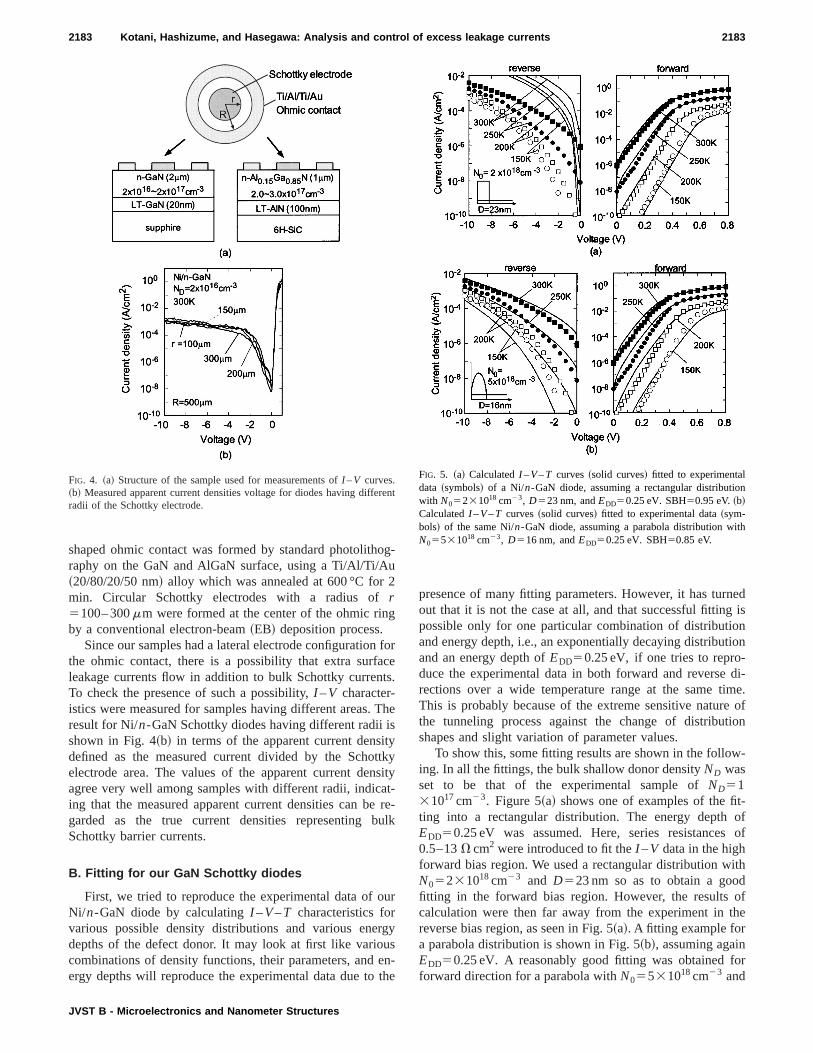
To show this, some fitting results are shown in the follow-ing. In all the fittings, the bulk shallow donor densityND wasset to be that of the experimental sample ofND5131017cm23. Figure 5~a! shows one of examples of the fit-ting into a rectangular distribution. The energy depth ofEDD50.25 eV was assumed. Here, series resistances of0.5–13V cm2 were introduced to fit theI –V data in the highforward bias region. We used a rectangular distribution withN05231018cm23 and D523 nm so as to obtain a goodfitting in the forward bias region. However, the results ofcalculation were then far away from the experiment in thereverse bias region, as seen in Fig. 5~a!. A fitting example fora parabola distribution is shown in Fig. 5~b!, assuming againEDD50.25 eV. A reasonably good fitting was obtained forforward direction for a parabola withN05531018cm23 and
FIG. 4. ~a! Structure of the sample used for measurements ofI –V curves.~b! Measured apparent current densities voltage for diodes having differentradii of the Schottky electrode.
FIG. 5. ~a! CalculatedI –V–T curves~solid curves! fitted to experimentaldata ~symbols! of a Ni/n-GaN diode, assuming a rectangular distributionwith N05231018 cm23, D523 nm, andEDD50.25 eV. SBH50.95 eV.~b!CalculatedI –V–T curves~solid curves! fitted to experimental data~sym-bols! of the same Ni/n-GaN diode, assuming a parabola distribution withN05531018 cm23, D516 nm, andEDD50.25 eV. SBH50.85 eV.
2183 Kotani, Hashizume, and Hasegawa: Analysis and control of excess leakage currents 2183
JVST B - Microelectronics and Nanometer Structures

D516 nm. However, fitting for reverseI –V–T characteris-tics was poor as shown in Fig. 5~b!. Attempts using a Gauss-ian distribution gave similar poor results. Many trials forfitting indicated that none of the peaked distributions shownin Fig. 3~b! were suitable for reproducing the experimentalI –V–T curves, even if the distribution parameters and theenergy depth of the defect level were changed over wideranges.
As a representative of the decaying distribution, two fit-ting results for an exponentially decaying distribution with ashallow energy depth ofEDD510 meV are compared in Figs.6~a! and 6~b!. By assumingN05331018cm23 and l530nm, we could obtain a reasonably good agreement in theforward direction. For the reverse bias region, however, thecalculation resulted in an extremely poor agreement, givingmuch larger magnitudes of currents with much weaker tem-perature dependence of currents than the experiment. Using aslightly different exponentially decaying distribution havingN05531018cm23 and l511 nm together with the sameshallow energy depth ofEDD510 meV, a reasonably goodfitting was found to be possible in the reverse direction, asshown in Fig. 6~b!. However, agreement in the forward di-rection became very poor.
After many trials, we obtained the best fitting result for
the Ni/GaN Schottky diode by assuming an exponential de-caying distribution shown in Fig. 7~a! with EDD50.25 eV.The fitting result is shown Fig. 7~b!. The simulation repro-duced forward and reverseI –V–T behavior almost com-pletely. For the same set of experimentalI –V–T data usedin this study, our previous analytical calculation7 for a rect-angular distribution of surface defect donors superposed onbulk uniform doping, resulted in an equally good fitting withthe experiment for the forward bias region. However, agree-ment was much poorer in the reverse direction. Furthermore,artificial connection of the approximate analytical formulasfor FE and TFE transport produced artificial kinks in thetheoretical curves for intermediate reverse biases7 similar tothe case of uniform doping mentioned above. The presentcomputer simulation solved all these problems.
It should be emphasized that, in order to achieve suchgood fitting for both forward and reverse directions simulta-neously over a wide temperature range, defect donors shouldhave a specific exponentially decaying distribution with aspecific energy depth. For three types of decaying distribu-tions of linearly decaying, quadratically decaying, and expo-nentially decaying distributions shown in Fig. 3~b!, fittingimproved with this order, and the best was obtained with theexponential distribution. Even for the exponential distribu-
FIG. 6. ~a! CalculatedI –V–T curves~solid curves! fitted to experimentaldata~symbols! of the Ni/n-GaN diode, assuming an exponentially decayingdistribution with N05331018 cm23, l530 nm, andEDD50.01 eV. SBH50.85 eV.~b! CalculatedI –V–T curves~solid curves! fitted to experimen-tal data~symbols! of the same Ni/n-GaN diode, assuming an exponentiallydecaying distribution with N05531018 cm23, l511 nm, and EDD
50.01 eV. SBH50.85 eV.
FIG. 7. ~a! Best choice of distribution shape and parameter values used toreproduce the experimental data of our Ni/n-GaN diode. SBH50.85 eV.~b!The result of fitting for various temperatures.~c! Calculated parameter sen-sitivities of current density againstN0 andl of the exponential distribution.
2184 Kotani, Hashizume, and Hasegawa: Analysis and control of excess leakage currents 2184
J. Vac. Sci. Technol. B, Vol. 22, No. 4, Jul ÕAug 2004

tion, choice of the parameter values was very critical. Toshow this, the parameter sensitivities of reverse current den-sity are plotted versus values ofN0 and l in Fig. 7~c! forvarious temperatures. The currents were very sensitive tochoice of bothN0 and l, especially in the low temperatureregion.
Similarly, it was found that the energy depthEDD shouldbe larger than 0.2 eV and below 0.35 eV to obtain acceptablefittings. The best value was 0.25 eV. Thus, the defect donor isa deep donor rather than a shallow donor. This value agreeswith the theoretical value obtained by the s-like donor modelfor N vacancy.17 In order to understand how the energy depthof the defect donor can be determined byI –V–T fitting, theshapes of the Schottky potential barriers were calculated forvarious values of energy depth. For example, calculated bar-rier shapes at the forward voltage of 0.3 V and at the tem-peratures of 150 and 300 K are compared in Fig. 8~a! for thecases ofEDD50.01 and 0.25 eV. The same exponentiallydecaying defect distribution shown in Fig. 7~a! with N05531018cm23 andl511 nm was assumed. It should be notedthat it is the same distribution used to obtain fitting shown inFig. 6~b!. In the case ofEDD50.01 eV, almost the same thinbarrier was formed at both temperatures due to the full ion-ization of shallow defect donor. This gave a larger magnitudeand weaker temperature dependence of calculated forwardcurrents than experimental ones, as seen in Fig. 6~b!. On theother hand, a much larger change of barrier profile was seenin the case ofEDD50.25 eV due to reduction of the densityof the ionized defect donors with decrease of temperature.This reduces tunneling current and increases its temperaturedependence at low temperatures, leading to a good fitting offorward current shown in Fig. 7~b!.
As for the reverse currents, the main feature of both ofexperimental and calculated currents shown in Fig. 7~b! isthat they show a large temperature dependence at small bi-ases, and temperature dependence is remarkably reduced asthe reverse bias is increased. To understand this behavior, theenergy distribution of electrons was calculated for differentbiases in terms of current density per unit energy as shown inFig. 8~b!. In all cases, distributions are nearly of Gaussianshape, as mentioned previously. However, its peak position isdependent on bias and temperature. When the reverse bias issmall, the peak position is considerably above the metalFermi level at 300 K, showing TFE transport, and it ap-proaches the metal Fermi level at 150 K, leading to FE trans-port. On the other hand, the peak is always close to the metalFermi level even at 300 K at large biases, and this gives aweak temperature dependence resulting from the FE trans-port. Thus, the anomalously large and weakly temperaturedependent reverse leakage current in GaN Schottky barriersis mainly due to field emission from the metal Fermi levelinto the semiconductor at large reverse biases through a thinsurface barrier which is further thinned down by a strongelectric field.
C. Fitting for GaN Schottky diodes reported inliterature
We also attempted to fit our calculation to experimentalI –V data of various GaN Schottky diodes reported by othergroups.
Figure 9~a! shows fitting results to the experimental dataon three different Pt/GaN diodes,S1 , S2 , andS3 . S1 is afterGuo et al.,1 S2 is after Schmitzet al.,2 andS3 was preparedin our laboratory. Pt was deposited by EB deposition forthree diodes. Excellent fitting was obtained for all threeI –Vdata by assuming the exponentially decaying distributionsshown on the right of Fig. 9~a!. The same energy depth ofEDD50.25 eV was used.
For comparison, the reverse current for the case of nodefect donor (N050) is shown by a dashed curve for thecase ofND5131017cm23. The experimental currents are7–8 orders of magnitude larger than the ideal case in allcases at high reverse biases. Detailed behavior of currents atlow biases is, however, considerably different among threediodes. To understand this, the calculated energy distribu-tions of tunneling electrons at a relatively small bias of21.5V are shown in Fig. 9~b!. In the case of theS1 diode, theGaN surface possesses the highest density of defect donorswith the shallowest distribution. This resulted in the thinnestbarrier width, leading to the highest Gaussian peak at a rela-tively high energy position, giving a large leakage currenteven at low biases. On the other hand, lower and wider dis-tributions of defect donors inS2 , and S3 diodes results inmuch smaller Gaussian peak heights, leading to smaller cur-rents. It is seen that slight change in the defect donor distri-bution sensitively changes the height and position of Gauss-ian peaks, indicating that details of distribution of the surfacedefect donors play a dominant role in determining leakagebehavior of GaN Schottky diodes.
FIG. 8. ~a! Calculated tunneling barrier profiles for the cases ofEDD
50.01 eV and 0.25 eV.~b! Calculated energy distributions of tunnelingelectrons for different biases and temperatures expressed in terms of thecurrent density per unit energy.
2185 Kotani, Hashizume, and Hasegawa: Analysis and control of excess leakage currents 2185
JVST B - Microelectronics and Nanometer Structures
Figures 10~a! and 10~b! show another result of fitting ofour theoretical curves to experimental forwardI –V–Tcurves of Au/n-GaN and Ag/n-GaN diodes reported by Yuet al.10 and Sawadaet al.,18 respectively. For fitting, expo-nential distributions shown in the insets of Figs. 10~a! and~b! with the energy depth ofEDD50.25 eV were used. Again,our simulation completely reproduced these forwardI –V–Tcurves.
D. Fitting for AlGaN Schottky diode
The I –V–T characteristics of Al0.15Ga0.85N Schottky di-odes were also investigated. As shown in Fig. 11~a!, the fab-ricated Ni/AlGaN diode exhibited large reverse leakage cur-rents with strong bias dependence and very smalltemperature dependence. The result of fitting is also shownin Fig. 11~a!. The spatial distribution and the energy depth ofthe surface defect donor, which gave the best fitting result,are shown in Fig. 11~b!. Again, good fitting was possibleonly for an exponentially decaying distribution of deep do-nors. We usedEDD50.37 eV obtained by our transient mea-surements on gateless AlGaN/GaN HFETs8 which alsoturned out to be the best value for fitting.
An extremely high density of the defect donors seems tobe present near the surface. This resulted in highly anoma-lous I –V–T characteristics of the Schottky diode with ex-cess leakage currents as observed as gate leakage in AlGaN/GaN HFETs.9 The origin of the defect donor seems again tobe N vacancy or its complex as discussed in Ref. 8.
E. Formation mechanism of defects and comparisonwith other models
All the successful fitting obtained here had the followingfeatures:~1! The exponentially decaying distribution fromsurface always gave the best fitting.~2! The best energydepth was always the same, beingEDD50.25 eV for GaNand 0.37 eV for Al0.15Ga0.85N. ~3! The best values ofN0 andl of the exponential distribution were, on the other hand,very different from sample to sample, ranging from 131018 to 431019cm23 for N0 and 3–30 nm forl with arough trend of large values ofN0 giving small values ofl.These features strongly indicate that the defect is the samefor all the samples, being most likely N vacancy or its relatedcomplex,7,8,19 as mentioned already. These defects must beintroduced from the surface either during crystal growth orduring processing. In fact, we have previously detected thepresence of a N vacancy related surface deep donors on themolecular beam epitaxy grown GaN surface by using aphotoluminescence-based technique.20 But, the density wasmuch smaller than the above numbers. The maximum pen-
FIG. 9. ~a! CalculatedI –V curves~solid curves! fitted to experimentalI –Vdata ~symbols! of three different Pt/n-GaN Schottky diodes produced inother laboratories (S1 ; Ref 1 andS2 ; Ref 2! as well as in ours (S3).Distributions of defect donors determined by best fitting are shown on theright. For comparison, calculatedI –V curve for the case of no defect (N0
50) is also shown forND5131017 cm23. ~b! Calculated energy distribu-tions of tunneling electrons atVg521.5 V for three diodes.
FIG. 10. Calculated forwardI –V curves~solid curves! fitted to experimentalforward I –V data ~symbols! of Au/n-GaN Schottky diodes reported byother workers~a! in Ref. 10 and~b! in Ref. 18. Distributions of defectdetermined by best fitting are shown in the insets.
2186 Kotani, Hashizume, and Hasegawa: Analysis and control of excess leakage currents 2186
J. Vac. Sci. Technol. B, Vol. 22, No. 4, Jul ÕAug 2004

etration depth ofl530 nm also seems to be too large for thecase of defect introduction during crystal growth.
As the formation mechanism of defect donors, we pro-pose that the defect donors in the Schottky barriers arelargely introduced during the process of deposition of metalby EB deposition, sputter deposition, or standard vacuumdeposition where the surface is hit by high-energy metal at-oms. In such cases, formation of process-induced deep levelsdepends on processing conditions, and can penetrate deepinto the bulk. In fact, defect formation into depths deeperthan 100 nm has been reported in the literature21–25 for EBdeposition and sputter-deposition processes applied to GaAsand GaN. Thus,l530 nm obtained by the present simulationis a very realistic value. The values of the integrated sheetdensity of defects given byN0l were in the range of 431012– 1.431013cm22 in our simulation, and these valuesagain seem to be typical numbers for process-induced de-fects. The observed rough trend of large values ofN0 givingsmall values ofl may be related to the thermal environmentfor processing such as substrate temperatures, annealing con-ditions, and cooling conditions. The exponentially decayingdensity distribution of defects, which was determined to bethe most likely distribution by fitting, seems also to be con-sistent with the picture of processing induced defects. This isbecause, if the excess energy for defect formation carried byhot phonons, hot electrons, and/or energetic atoms, decays ata constant rate from surface into bulk, the distribution ofdensity of defects which is proportional to energy loss, willalso be an exponential one. Thus, the present simulationbased on the TSB model together with metal-deposition in-duced formation of N vacancy or its complex seems to becapable of explaining all the aspects of experimental obser-vation.
Finally, let us comment briefly on other models on reverseleakage currents in nitride based Schottky diodes. Several
groups qualitatively suggested a trap-assisted tunnelingmechanism for excess leakage currents in the reverse biasregion.3,10,11 Here, the presence of discrete deep-level statesor a continuum of trap states near the Schottky interface isassumed, and they are supposed to provide tunneling pathsthrough the energy barrier after capture of electrons by ther-mal excitation. However, it is difficult to explain the ob-served large leakage currents by such a two-step or multistepprocess involving carrier capture by defects with small cap-ture cross sections. Additionally, at low temperatures, thethermal excitation process of electrons from metal to highertrap levels would be suppressed and the current should belimited with the FE process. Experimentally, however, cur-rents were far larger the prediction by the FE mechanism, aswas shown in Fig. 2~b!. Very recently, Karmalkar andco-workers12 tried to fit the gate leakage current of AlGaN/GaN HFETs by the calculation based on the trap-assistedtunneling model under the unlikely assumption of a defectcontinuum with wide energy band widths. One has to assumea continuum with energy widths of 0.66–0.90 eV extendingthroughout the depletion region of the semiconductor. Thisassumption is unacceptable because there has been no directexperimental evidence for the existence of such a peculiardefect continuum.
IV. SUPPRESSION OF REVERSE LEAKAGECURRENTS
According to the discussion in the previous section, high-energy metal atoms most likely cause the escape of N atomsfrom the surface during the metal deposition processes, andintroduce N–vacancy-related deep donor levels near theSchottky interface. Based on this idea, we explored two pos-sibilities of reducing leakage currents. One is the use of alow-energy electrochemical metal deposition process, andthe other is to insert a high quality buffer layer at theSchottky interface to avoid direct bombardment by high-energy metal atoms.
Figure 12~a! shows theI –V curves of Pt/n-GaN Schottkydiodes fabricated by a standard EB deposition process and bythe electrochemical process whose details are given in Ref.26. As mentioned in Sec. III B, the diode fabricated by theEB process exhibited large leakage currents at the reversebias region due to the existence of high density of the surfacedefect donor. On the other hand, a remarkable suppression ofleakage current was observed for the diode formed by thelow-energy/low-temperature electrochemical process. Thesimulation of itsI –V curve showed that the electrochemicalprocess can dramatically suppress the generation of the de-fect donors. Very recently, Miller and co-workers27 also re-ported about 3 orders reduction of reverse-bias leakage cur-rent in a Ni/n-GaN diode by an electrochemical treatment inNaOH solution at 30 °C. However, they argued that forma-tion of a thin oxide layer~Ga oxide! during the treatment wasresponsible for the reduction of leakage currents.
Suppression of leakage current was also attempted by in-sertion of an ultrathin Al2O3 passivation film which we haverecently developed for GaN and AlGaN surfaces.28,29 The
FIG. 11. ~a! CalculatedI –V curves~solid curves! fitted to experimentalI –Vdata~symbols! of a Ni/n-Al0.15Ga0.85N Schottky diode. SBH51.14 eV.~a!Best choice of distribution shape and parameter values used to obtain~a!.
2187 Kotani, Hashizume, and Hasegawa: Analysis and control of excess leakage currents 2187
JVST B - Microelectronics and Nanometer Structures

process sequence was as follows. First, the AlGaN surfacewas treated in the electron cyclotron resonance~ECR! N2
plasma at 280 °C for 1 min. This treatment partially recoversor terminates the N vacancy-related surface defects, leadingto reduction of surface-defect traps and surface states onAlGaN.30 Then, an Al layer with a nominal thickness of 1 nmwas deposited by molecular beam deposition at room tem-perature, followed by its oxidation using ECR-excited O2
plasma. Finally, the sample was annealed at 700 °C for 10min under ultrahigh vacuum condition. Figure 12~b! com-pares theI –V curves of Ni/n-Al0.15Ga0.85N Schottky diodeswith and without 1 nm thick Al2O3 film. More than 2 ordersof magnitude reduction of leakage current was observed forthe diode with the Al2O3 passivation layer. The simulationresult indicated that the N vacancy-related defect was greatlyreduced by the insertion of a thin Al2O3 layer as shown onthe right of Fig. 12~b!.
V. CONCLUSION
Attempts were made to perform a rigorous computersimulation of the current transport in GaN and AlGaNSchottky diodes on the basis of the TSB model. First a simu-lation program for current transport of a Schottky barrierhaving an arbitrary potential profile was developed. Then, it
was applied to calculation ofI –V curves for various spatialdensity distributions and various energy depths of defect do-nors on the basis of the TSB model. As a result, by assumingpresence of N vacancy-related deep donors with an exponen-tially decaying density distribution from the surface, thesimulation reproduced almost perfectly experimentalI –V–Tcurves of GaN and AlGaN Schottky diodes measured by ourgroup as well as by other groups. This clearly proves thevalidity of the TSB model as the mechanism of anomalouslylarge current leakage in nitride-based Schottky diodes. At-tempts were also made to suppress surface defect donors atthe GaN and AlGaN surfaces. A low-energy electrochemicalmetal deposition and a metal–insulator–semiconductorSchottky structure using an ultrathin Al2O3 film realized 2–3orders of magnitude reduction of leakage currents, indicatingvery large reduction of deep defect donors.
ACKNOWLEDGMENT
This work is supported in part by the 21 Century COEprogram of ‘‘Meme-Media Technology Approach to theR&D of Next-Generation ITs’’ from MEXT, Japan.
1J. D. Guo, M. S. Feng, R. J. Guo, F. M. Pan, and C. Y. Chang, Appl. Phys.Lett. 67, 2657~1995!.
2A. C. Schmitz, A. T. Ping, M. A. Kahn, Q. Chen, J. W. Yang, and I.Adesida, J. Electron. Mater.27, 255 ~1998!.
3J. C. Carrano, T. Li, P. A. Grudowski, C. J. Eiting, R. D. Dupuis, and J. C.Cambell, Appl. Phys. Lett.72, 542 ~1998!.
4X. A. Cao, S. J. Pearton, G. Dang, A. P. Zhang, F. Ren, and J. M. VanHove, Appl. Phys. Lett.75, 4130~1999!.
5E. Monroyet al., Phys. Status Solidi A188, 367 ~2001!.6S. Oyama, T. Hashizume, and H. Hasegawa, Appl. Surf. Sci.190, 322~2002!.
7H. Hasegawa and S. Oyama, J. Vac. Sci. Technol. B20, 1647~2002!.8H. Hasegawa, T. Inagaki, S. Ootomo, and T. Hashizume, J. Vac. Sci.Technol. B21, 1844~2003!.
9S. Mizuno, Y. Ohno, S. Kishimoto, K. Maezawa, and T. Mizutani, Jpn. J.Appl. Phys., Part 141, 5125~2002!.
10L. S. Yu, Q. Z. Liu, Q. J. Xing, D. J. Qiao, S. S. Lau, and J. Redwing, J.Appl. Phys.84, 2099~1998!.
11E. J. Miller, X. Z. Dang, and E. T. Yu, J. Appl. Phys.88, 5951~2000!.12S. Karmalkar, D. M. Sathaiya, and M. S. Shur, Appl. Phys. Lett.82, 3976
~2003!.13R. Stratton, J. Phys. Chem. Solids23, 1177~1962!.14F. A. Padovani and R. Stratton, Solid State Electron9, 695 ~1966!.15J. Neugebauer and C. G. Van de Walle, Phys. Rev. B50, 8067~1994!.16P. Boguslauski, E. L. Briggs, and J. Bernholc, Phys. Rev. B51, 17255
~1995!.17E. Yamaguchi and M. R. Junnarkar, J. Cryst. Growth189Õ190, 570
~1998!.18T. Sawada, Y. Ito, K. Imai, K. Suzuki, H. Tomozawa, and S. Sakai, Appl.
Surf. Sci.159–160, 449 ~2000!.19H. Hasegawa and T. Hashizume, Mater. Res. Soc. Symp. Proc.743, 45
~2003!.20M. Konishi, T. Hashizume, and H. Hasegawa, Inst. Phys. Conf. Ser.170,
837 ~2002!.21F. D. Auret, S. A. Goodman, G. Myberg, F. K. Koschnik, J. M. Spaeth, B.
Beaumont, and P. Gibart, Physica B273–274, 84 ~1999!.22F. D. Auret, S. A. Goodman, F. K. Koschnik, J. M. Spaeth, B. Beaumont,
and P. Gibart, Appl. Phys. Lett.74, 2173~1999!.23D. C. Look and Z. Q. Fang, Appl. Phys. Lett.79, 84 ~2001!.24R. Kleinhenz, P. M. Mooney, C. P. Schneider, and O. Paz,Proceedings of
the 13th International Conference on Defects in Semiconductors, editedby L. C. Kimering and J. M. Parsey~Metallurgical Society of AIME, NewYork, 1985!, p. 627.
25M. Nel and F. D. Auret, J. Appl. Phys.64, 2422~1988!.
FIG. 12. ~a! Experimental and calculatedI –V curves for Pt/n-GaN Schottkydiodes fabricated by a standard EB deposition process and by the electro-chemical process.~b! Experimental and calculatedI –V curves ofNi/n-Al0.15Ga0.85N Schottky diodes with and without 1 nm thick Al2O3
passivation film. Distributions of defect donors determined by best fittingare shown on the right.
2188 Kotani, Hashizume, and Hasegawa: Analysis and control of excess leakage currents 2188
J. Vac. Sci. Technol. B, Vol. 22, No. 4, Jul ÕAug 2004

26H. Hasegawa and T. Sato, J. Vac. Sci. Technol. B15, 1227~1997!.27E. J. Miller, D. M. Schaadt, E. T. Yu, P. Waltereit, C. Poblenz, and J. S.
Speck, Appl. Phys. Lett.82, 1293~2003!.28T. Hashizume, S. Ootomo, T. Inagaki, and H. Hasegawa, J. Vac. Sci.
Technol. B21, 1828~2003!.
29T. Hashizume, S. Ootomo, and H. Hasegawa, Appl. Phys. Lett.83, 2952~2003!.
30T. Hashizume, S. Ootomo, S. Oyama, M. Konishi, and H. Hasegawa, J.Vac. Sci. Technol. B19, 1675~2001!.
2189 Kotani, Hashizume, and Hasegawa: Analysis and control of excess leakage currents 2189
JVST B - Microelectronics and Nanometer Structures