analog to digital converters - school of electrical ...rhabash/elg3336lnconveters.pdf6 an adc is...
TRANSCRIPT
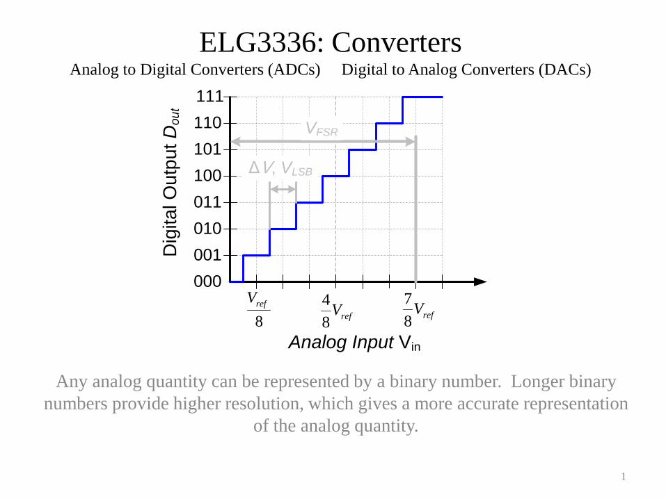
ELG3336: Converters Analog to Digital Converters (ADCs) Digital to Analog Converters (DACs)
1
Any analog quantity can be represented by a binary number. Longer binary
numbers provide higher resolution, which gives a more accurate representation
of the analog quantity.
000
001
010
011
100
101
110
111
8
refV
Dig
ita
l O
utp
ut D
ou
t
Analog Input Vin
7
8refV
4
8refV
ΔV, VLSB
VFSR

Analog to Digital Converters
Objective: Representing an analog varying physical quantity by a sequence of discrete numerical values.
2
01 07 10 15 09 03 00 05
Sample
& Hold
Quantizationfsample
Analog Digital

3
Successive Approximation ADC
• Generate internal analog signal VD/A
• Compare VD/A with input signal Vin
• Modify VD/A by D0D1D2…DN-1 until closest possible value to Vin
is reached
S&HLogic
DAC
D0 D1 DN-1
Vin
Vref
VD/A
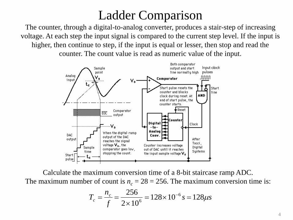
Ladder Comparison The counter, through a digital-to-analog converter, produces a stair-step of increasing
voltage. At each step the input signal is compared to the current step level. If the input is
higher, then continue to step, if the input is equal or lesser, then stop and read the
counter. The count value is read as numeric value of the input.
4
Calculate the maximum conversion time of a 8-bit staircase ramp ADC.
The maximum number of count is nc = 28 = 256. The maximum conversion time is:
ssf
nT c
c 12810128102
256 6
6

Flash ADC
Vin
Vref
Over range
D0
D1
DN-1
(2N-1) to N
encoder
R/2
R
R/2
R
R
R
R
R
R
• Vin connected with 2N comparators in parallel
• Comparators connected to resistor string
If Output
VIN > VREF High
VIN < VREF Low

6
An ADC is usually in form of an integrated circuit (IC). ADC0808
and ADC0809 are two typical examples of 8-bit ADC with 8-
channel multiplexer using successive approximation method for its
conversion.
ADC0809
National
Semiconductor
For more information,
http://www.national.com/ads-cgi/viewer.pl/ds/AD/ADC0808.pdf
7
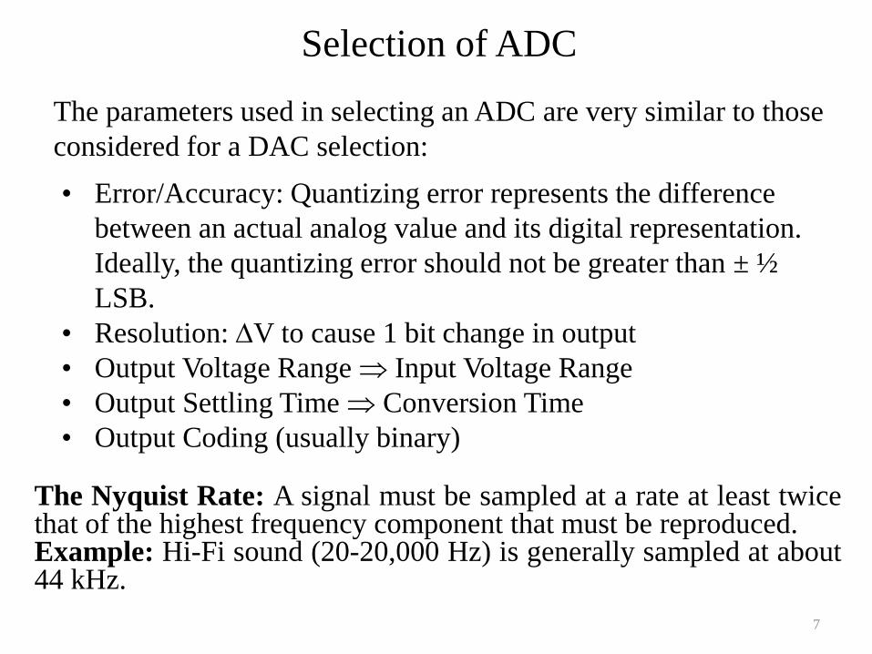
Selection of ADC
The parameters used in selecting an ADC are very similar to those
considered for a DAC selection:
• Error/Accuracy: Quantizing error represents the difference
between an actual analog value and its digital representation.
Ideally, the quantizing error should not be greater than ± ½
LSB.
• Resolution: DV to cause 1 bit change in output
• Output Voltage Range Input Voltage Range
• Output Settling Time Conversion Time
• Output Coding (usually binary)
The Nyquist Rate: A signal must be sampled at a rate at least twice that of the highest frequency component that must be reproduced. Example: Hi-Fi sound (20-20,000 Hz) is generally sampled at about 44 kHz.
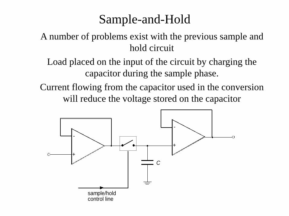
Sample-and-Hold
A number of problems exist with the previous sample and
hold circuit
Load placed on the input of the circuit by charging the
capacitor during the sample phase.
Current flowing from the capacitor used in the conversion
will reduce the voltage stored on the capacitor
-
+
-
+
sample/hold control line
C
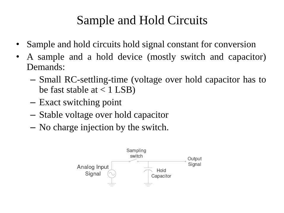
Sample and Hold Circuits
• Sample and hold circuits hold signal constant for conversion
• A sample and a hold device (mostly switch and capacitor) Demands:
– Small RC-settling-time (voltage over hold capacitor has to be fast stable at < 1 LSB)
– Exact switching point
– Stable voltage over hold capacitor
– No charge injection by the switch.
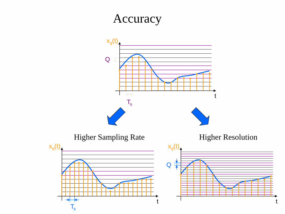
t Ts
Q
xq(t)
Accuracy
t Ts
xq(t)
Higher Sampling Rate
t
Q
xq(t)
Higher Resolution
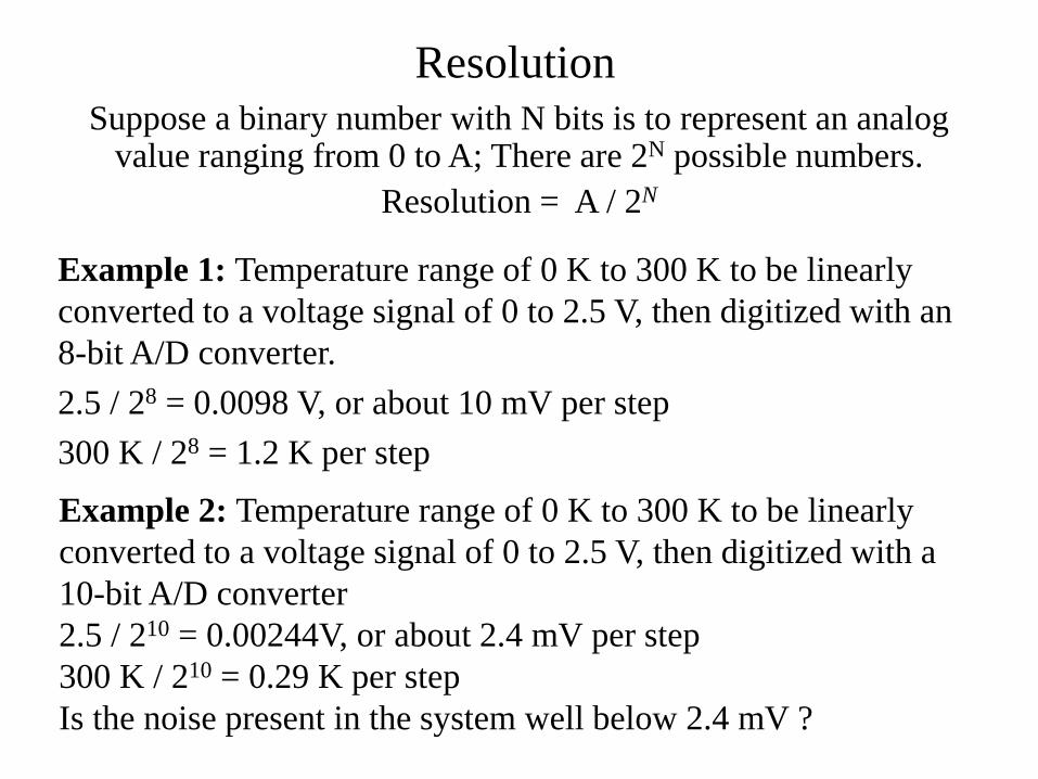
Resolution Suppose a binary number with N bits is to represent an analog
value ranging from 0 to A; There are 2N possible numbers.
Resolution = A / 2N
Example 1: Temperature range of 0 K to 300 K to be linearly
converted to a voltage signal of 0 to 2.5 V, then digitized with an
8-bit A/D converter.
2.5 / 28 = 0.0098 V, or about 10 mV per step
300 K / 28 = 1.2 K per step
Example 2: Temperature range of 0 K to 300 K to be linearly
converted to a voltage signal of 0 to 2.5 V, then digitized with a
10-bit A/D converter
2.5 / 210 = 0.00244V, or about 2.4 mV per step
300 K / 210 = 0.29 K per step
Is the noise present in the system well below 2.4 mV ?
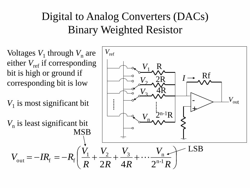
Digital to Analog Converters (DACs)
Binary Weighted Resistor
R
V
R
V
R
V
R
VRIRV
1-n
n321ffout
242
MSB
LSB
Voltages V1 through Vn are
either Vref if corresponding
bit is high or ground if
corresponding bit is low
V1 is most significant bit
Vn is least significant bit
I
- +
R
2R
4R
2n-1R
Rf
Vout
Vref
V1
V2
V3
Vn
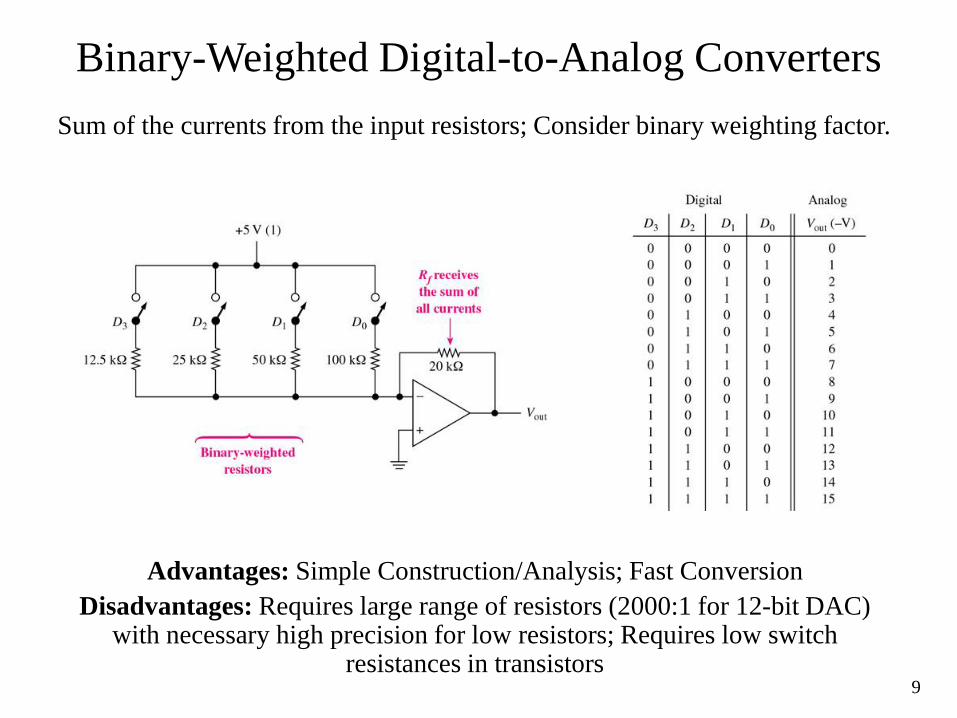
Binary-Weighted Digital-to-Analog Converters
Sum of the currents from the input resistors; Consider binary weighting factor.
9
Advantages: Simple Construction/Analysis; Fast Conversion
Disadvantages: Requires large range of resistors (2000:1 for 12-bit DAC) with necessary high precision for low resistors; Requires low switch
resistances in transistors

Binary Weighted Resistor
Rf = R
8R 4R 2R R Vo
-VREF
iI
LSB
MSB
R
B
R
B
R
B
R
BVI REF
842
0123
842
0123
BBBBVRIV REFfOUT
ResolutionValue Digital
2 1
REF
in
iREFOUT
V
BVV

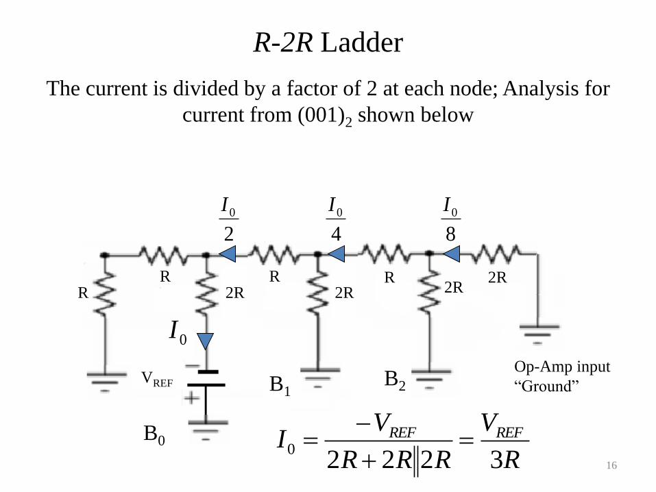
R-2R Ladder
• The less significant the bit, the more resistors the signal muss pass through before reaching the op-amp
• The current is divided by a factor of 2 at each node
LSB MSB
16
R-2R Ladder
The current is divided by a factor of 2 at each node; Analysis for
current from (001)2 shown below
0I
VREF
R R R R 2R
2R 2R 2R
Op-Amp input
“Ground”
B0
2
0I
4
0I
8
0I
R
V
RRR
VI REFREF
32220
B1 B2
17
0I
VREF
R R R R 2R
2R 2R 2R
Op-Amp input
“Ground”
B0 B2
0I
VREF
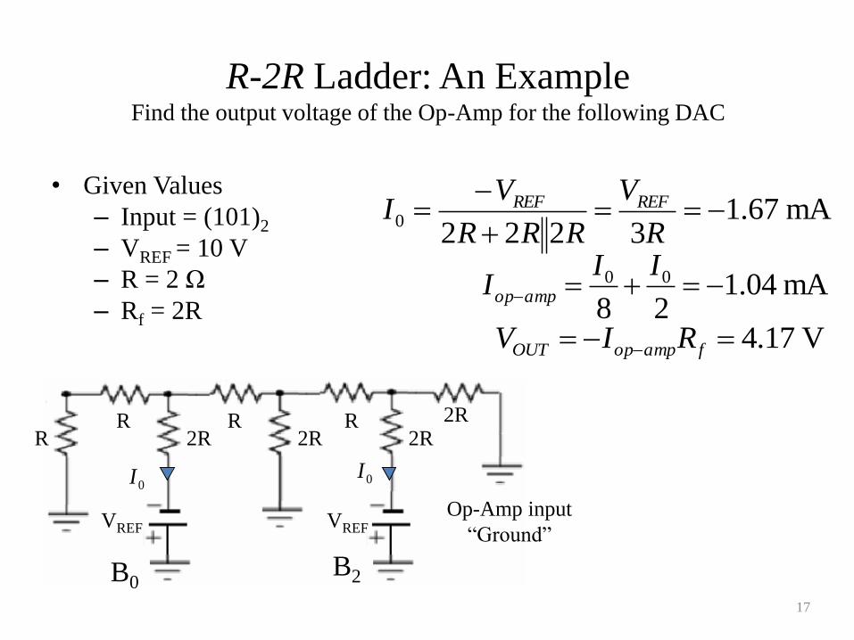
R-2R Ladder: An Example Find the output voltage of the Op-Amp for the following DAC
• Given Values
– Input = (101)2
– VREF = 10 V
– R = 2 Ω
– Rf = 2R
mA67.13222
0
R
V
RRR
VI REFREF
mA04.128
00
III ampop
V17.4 fampopOUT RIV
18
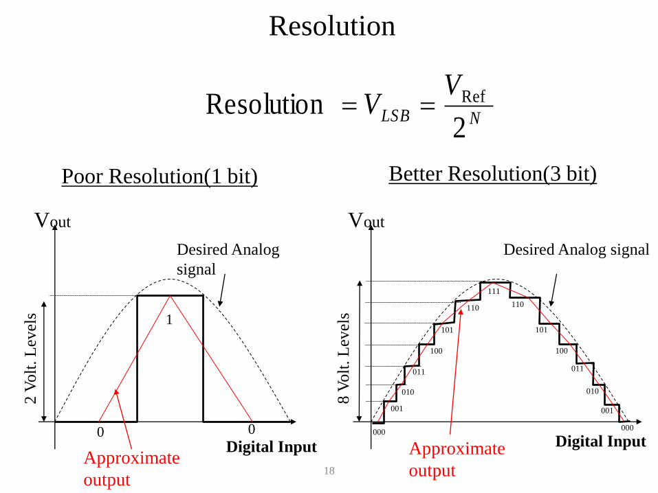
Resolution
Better Resolution(3 bit) Poor Resolution(1 bit)
Vout
Desired Analog
signal
Approximate
output
2 V
olt
. L
evel
s
Digital Input 0 0
1
Digital Input
Vout
Desired Analog signal
Approximate
output
8 V
olt
. L
evel
s
000
001
010
011
100
101
110
111
110
101
100
011
010
001
000
NLSB
VV
2Resolution Ref
19
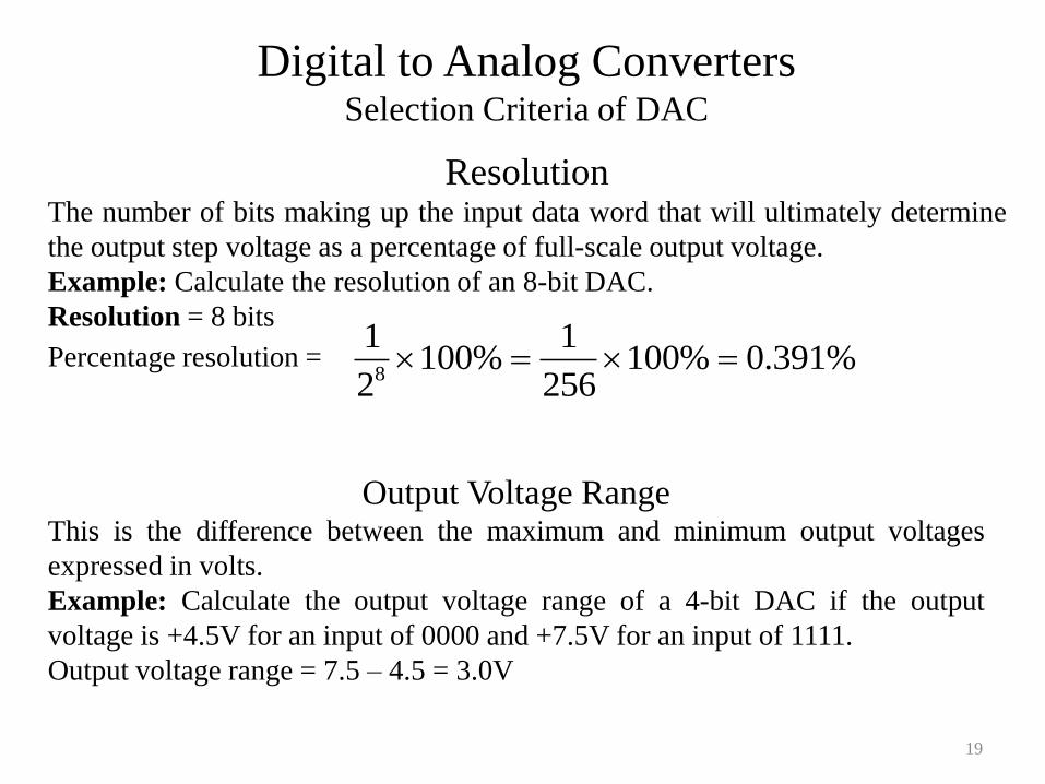
Digital to Analog Converters Selection Criteria of DAC
Resolution The number of bits making up the input data word that will ultimately determine
the output step voltage as a percentage of full-scale output voltage.
Example: Calculate the resolution of an 8-bit DAC.
Resolution = 8 bits
Percentage resolution = %391.0%100256
1%100
2
18
Output Voltage Range This is the difference between the maximum and minimum output voltages
expressed in volts.
Example: Calculate the output voltage range of a 4-bit DAC if the output
voltage is +4.5V for an input of 0000 and +7.5V for an input of 1111.
Output voltage range = 7.5 – 4.5 = 3.0V
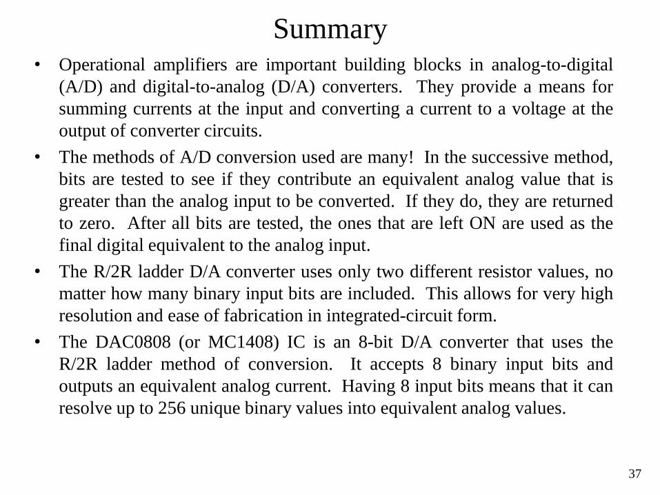
Summary • Operational amplifiers are important building blocks in analog-to-digital
(A/D) and digital-to-analog (D/A) converters. They provide a means for
summing currents at the input and converting a current to a voltage at the
output of converter circuits.
• The methods of A/D conversion used are many! In the successive method,
bits are tested to see if they contribute an equivalent analog value that is
greater than the analog input to be converted. If they do, they are returned
to zero. After all bits are tested, the ones that are left ON are used as the
final digital equivalent to the analog input.
• The R/2R ladder D/A converter uses only two different resistor values, no
matter how many binary input bits are included. This allows for very high
resolution and ease of fabrication in integrated-circuit form.
• The DAC0808 (or MC1408) IC is an 8-bit D/A converter that uses the
R/2R ladder method of conversion. It accepts 8 binary input bits and
outputs an equivalent analog current. Having 8 input bits means that it can
resolve up to 256 unique binary values into equivalent analog values.
37