analog to digital converter(adc) and digital to analog...
TRANSCRIPT

1
Analog to Digital Converter(ADC)
and
Digital to Analog Converter (DAC)

2
Analog I/O
• Analog inputs – convert to digital using an Analog
to Digital converter (A/D or ADC)
• Analog output – convert digital output to analog
using a Digital to Analog converter (D/A or DAC)
• A/D outputs and D/A inputs can be attached to
digital I/O ports
• Design issues to consider – number of bits of
accuracy, conversion time delay, and sample rate
needed by application

3
The MCP3008 10-bit 200Ksps A/D chip used in Phidget modules has an SPI interface.

4
Off-the-shelf ADC
• Resolution – smallest distinguishable change in input
• Precision – number of distinguishable inputs
• Accuracy – the absolute error of the entire system
• Monotonic – no missing codes
• Linear – constant resolution
• Speed – time to convert

5
Analog-digital interface

6
Processing analog signal

7
Analog input signal

8
Analog input signal
• For periodic waveforms, the duration of
the waveform before it repeats is called
the period of the waveform
• The rate at which a regular vibration
pattern repeats itself (frequency =
1/period)

9
Frequency of a Waveform
• The unit for frequency is cycles/second,
also called Hertz (Hz).
• The frequency of a waveform is equal to
the reciprocal of the period.
frequency = 1/period

10
Frequency of a Waveform
• Examples:
frequency = 10 Hz
period = .1 (1/10) seconds
frequency = 100 Hz
period = .01 (1/100) seconds
frequency = 261.6 Hz (middle C)
period = .0038226 (1/ 261.6) seconds

11
Waveform Sampling (Quantization)
• To represent waveforms on digital computers,
we need to digitize or sample the waveform.
• side effects of digitization:
– introduces some noise
– limits the maximum upper frequency range

12
Sampling rate
• The sampling rate (SR) is the rate at which
amplitude values are digitized from the
original waveform.
– CD sampling rate (high-quality):
SR = 44,100 samples/second
– medium-quality sampling rate:
SR = 22,050 samples/second
– phone sampling rate (low-quality):
SR = 8,192 samples/second

13
Sampling rate
• Higher sampling rates
allow the waveform to
be more accurately
represented

14
Nyquist Theorem
• Nyquist Theorem:
We can digitally represent only frequencies up to half the sampling rate.
– Example:
CD: SR=44,100 Hz
Nyquist Frequency = SR/2 = 22,050 Hz
– Example:
SR=22,050 Hz
Nyquist Frequency = SR/2 = 11,025 Hz

15
Nyquist Theorem
Sampling rate (SR) > 2 fmax
fmax is the largest signal frequency of interest
16
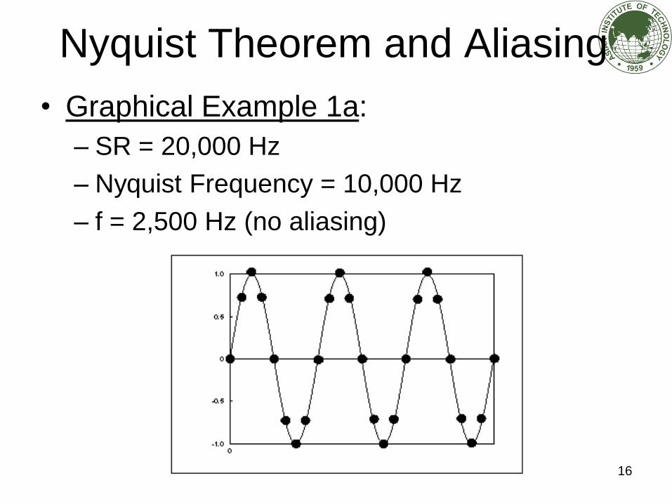
Nyquist Theorem and Aliasing
• Graphical Example 1a:
– SR = 20,000 Hz
– Nyquist Frequency = 10,000 Hz
– f = 2,500 Hz (no aliasing)

17
Nyquist Theorem and Aliasing
• Graphical Example 1b:
– SR = 20,000 Hz
– Nyquist Frequency = 10,000 Hz
– f = 5,000 Hz (no aliasing)
(left and right figures have same frequency, but have
different sampling points)

18
Nyquist Theorem and Aliasing
• Graphical Example 2:
– SR = 20,000 Hz
– Nyquist Frequency = 10,000 Hz
– f = 10,000 Hz (no aliasing)

19
Nyquist Theorem and Aliasing
• Graphical Example 2:
– BUT, if sample points fall on zero-crossings
the sound is completely cancelled out

20
Nyquist Theorem and Aliasing
• Graphical Example 3:
– SR = 20,000 Hz
– Nyquist Frequency = 10,000 Hz
– f = 12,500 Hz, f' = 7,500

21
Nyquist Theorem and Aliasing
• Graphical Example 3:
– Fitting the simplest sine wave to the sampled
points gives an aliased waveform (dotted line
below):

22
Sample of sine wave at different
freq.

23
Processing analog signal

24
Low pass filter
• Allow only low
frequency value to
pass
• Prevent aliasing

25
Layout of ADC

26
ADC precision
• Number of ADC bit output (n):
n = input range (r) / input resolution y
E.g., input range of 1, and resolution of 0.0001
n = 10000 alternatives or 15 bits value
Assume linear ADC

27
Sample and hold circuit

28
Sample and hold circuit
• Using op-amp to hold signal strength
unity gain buffer
Vin
Vout
control
+
-
+
-

29
Sample and hold signal

30
Hold circuit output

31
Quantized output

32
Convert analog value to digital
value
Bipolar codes Offset binary 2s binary
+5.00 1111 0111
+2.50 1100 0100
+0.04 1000 0000
+0.00 1000 0000
-2.50 0100 1100
-5.00 0000 1000

33
ADC types
• Flash ADC
- fast
• Successive Approximation ADC
- most popular
• Sigma Delta ADC
- highest output precision

34
Flash ADC
• Use reference voltage and differential op-
amp to generate digital output
• Fast conversion
• To increase the number of bits, it requires
larger hardware support

35
Two-bit flash ADC
Vin X3 X2 X1 Z1 Z0
V<2.5 0 0 0 0 0
2.5V<5.0 0 0 1 0 1
5.0V<7.5 0 1 1 1 0
V 7.5 1 1 1 1 1
+
-
+
-
+
-
REF
20 k
10V
20 k
20 k
20 k Vin
20 k
5V
20 k
5V
20 k
5V
Z1
Z0
2.5V
5.0V
7.5VX3
X2
X1

36
Flash converter

37
256R ladder network

38
Successive Approximation ADC
• Similar to Flash ADC, but use only one set
of hardware
• Require longer time
• Fixed size of hardware
• Widely used

39
Successive Approximation ADC
Vin
+
-
N bit
Successive
Approximation
Clock
Done
Go
N bit
ADC
n
5V
Digital
output

40
The MCP3008 10-bit 200Ksps A/D chip used in Phidget modules has an SPI interface.

41
Successive approximation counting

42
Block diagram of internal AD
converter

43
AD converter

44
3-bit AD converter

45
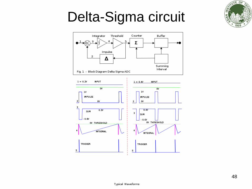
Delta-Sigma ADC
• Quantization noise is uniformly distributed
among frequency spectrum
• Using over-sampling technique to reduce the
impact of quantization noise
• Results in higher bit-precision
• Slow

46
Frequency domain

47
Oversampling by K times

49
Signal pin of AD converter

ARM Cortex ADC support
• 12 bit ADC is successive approximation
• 18 multiplexed channel (16 external and 2
internal)
• The result is stored in a left-aligned or right
aligned 16 bit register
• Analog watchdog feature allows the
application to detect if input voltage goes
outside user defined high or low threshold
• ADC input clock is generated from PCLK2 50

ADC for STM32F4xx
• ADC can be power-on by setting ADON bit
in ADC_CR1 control register. It will wake
up ADC from power down mode
• Then, we need to set ADON bit again to
start analog conversion
51

Single ADC block diagram
52
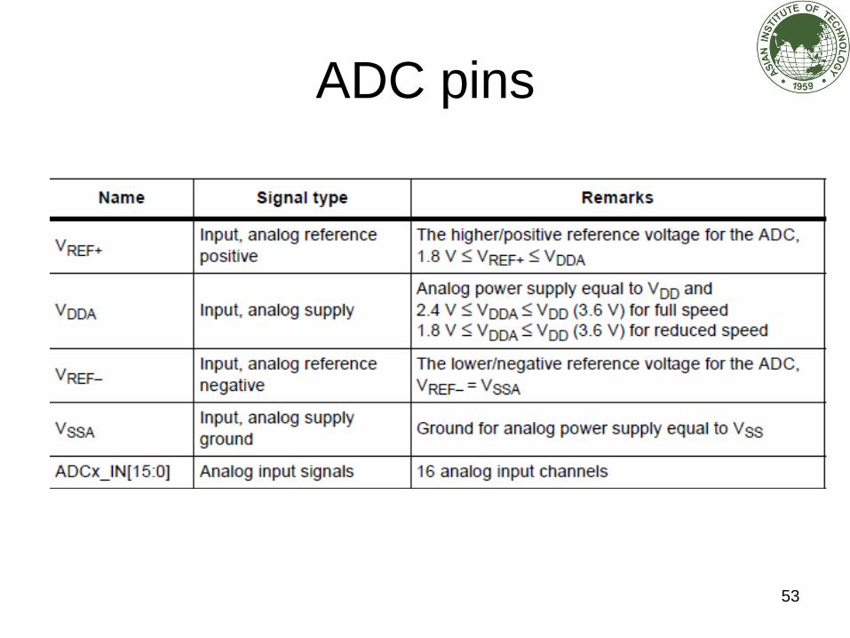
ADC pins
53

Timing diagram
54

Analog watchdog
55

Temperature sensor and Vref
diagram
56
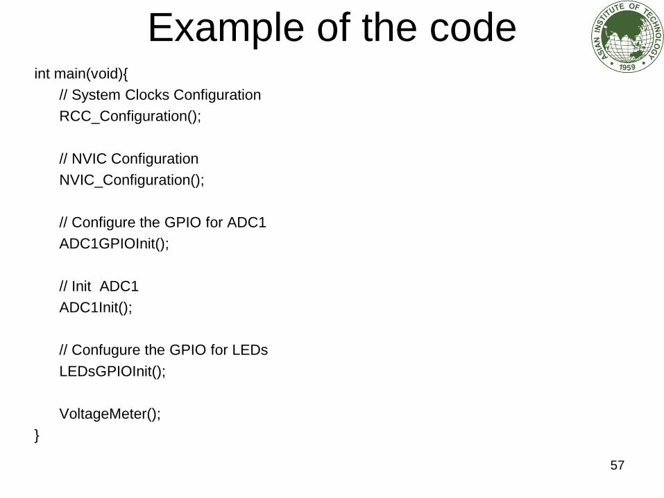
Example of the code int main(void){
// System Clocks Configuration
RCC_Configuration();
// NVIC Configuration
NVIC_Configuration();
// Configure the GPIO for ADC1
ADC1GPIOInit();
// Init ADC1
ADC1Init();
// Confugure the GPIO for LEDs
LEDsGPIOInit();
VoltageMeter();
}
57

void ADC1GPIOInit(void)
{
GPIO_InitTypeDef GPIO_InitStructure;
// Enable ADC1 clock
RCC_APB2PeriphClockCmd(RCC_APB2Periph_ADC1, ENABLE);
// Config PA1 as analog input
GPIO_InitStructure.GPIO_Pin = GPIO_Pin_1;
GPIO_InitStructure.GPIO_Speed = (GPIOSpeed_TypeDef)0;
GPIO_InitStructure.GPIO_Mode = GPIO_Mode_AIN;
GPIO_Init (GPIOA, &GPIO_InitStructure);
}
58

void ADC1Init(void){
ADC_InitTypeDef ADC_InitStructure;
/* ADC1 is configured as follow:
- Single channel, single conversion mode
- Output data aligned left */
ADC_InitStructure.ADC_Mode = ADC_Mode_Independent;
ADC_InitStructure.ADC_ScanConvMode = DISABLE;
ADC_InitStructure.ADC_ContinuousConvMode = DISABLE;
ADC_InitStructure.ADC_ExternalTrigConv = ADC_ExternalTrigConv_None;
ADC_InitStructure.ADC_DataAlign = ADC_DataAlign_Left;
ADC_InitStructure.ADC_NbrOfChannel = 1;
// Do it from scratch
ADC_DeInit(ADC1);
ADC_Init(ADC1, &ADC_InitStructure);
59

// Enable the ADC
ADC_Cmd(ADC1, ENABLE);
// ADC calibration
ADC_ResetCalibration(ADC1); // Enable ADC1 reset calibration
while(ADC_GetResetCalibrationStatus(ADC1) == SET);
ADC_StartCalibration(ADC1); // Start ADC calibration
while(ADC_GetCalibrationStatus(ADC1) == SET);
// Configure channel to sampling rate of 55.5 cycle
ADC_RegularChannelConfig(ADC1, 1, 1, ADC_SampleTime_55Cycles5);
}
60

void LEDsGPIOInit(void){
GPIO_InitTypeDef GPIO_InitStructure;
// Initial LED PB[8..15]
RCC_APB2PeriphClockCmd(RCC_APB2Periph_GPIOB, ENABLE);
GPIO_InitStructure.GPIO_Speed = GPIO_Speed_50MHz;
GPIO_InitStructure.GPIO_Mode = GPIO_Mode_Out_PP;
GPIO_InitStructure.GPIO_Pin = GPIO_Pin_8 |
GPIO_Pin_9 |GPIO_Pin_10 | GPIO_Pin_11 |
GPIO_Pin_12 | GPIO_Pin_13 |GPIO_Pin_14 |GPIO_Pin_15;
GPIO_Init(GPIOB, &GPIO_InitStructure);
}
61

void VoltageMeter(void){
u16 currentReading = 0;
u8 first8bits = 0;
while(1){
currentReading = GetADC1Channel1();
// Get only higher byte
first8bits = currentReading >> 8;
OutputLEDs(first8bits);
}
}
u16 GetADC1Channel1(void){
// Configure channel
ADC_RegularChannelConfig(ADC1, 1, 1, ADC_SampleTime_55Cycles5);
// Start the conversion
ADC_SoftwareStartConvCmd(ADC1, ENABLE);
// Wait until conversion completion
while(ADC_GetFlagStatus(ADC1, ADC_FLAG_EOC) == RESET);
// Get the conversion value
return ADC_GetConversionValue(ADC1);
}
62

Simulink
• ADC block can be used to generate
analog signal
63

Configurations
64

Configurations
• ADC modules: There are 3 modules
available
• Output data type: double/single/raw(int16)
• ADC Prescaler : ADC clock prescaler
The block outputs digital value between 0 to
4095.
65

Example
66

Digital to Analog Converter
(DAC)
67

68
Layout of DAC

69
Analog of digital conversion

70
Analog voltage of zero order

71
Reconstruction

72
Summing Amplifier
• Scale factors for the 2
inputs can be
independently adjusted by
proper choice of R2 and R1.
• Any number of inputs can
be connected to summing
junction through extra
resistors.
• This is an example of a
simple digital-to-analog
converter.
1
1v
1i
R
2
2v
2i
R
3
ov3
iR
Since negative amplifier input is
at virtual ground,
Since i-=0, i3= i1 + i2,
2v
2
31
v
1
3ov
R
R
R
R
Chap 11-72

73
Binary weight register method

74
DA converter

75
DA pin signal

76
Connection of DAC

77
Analog interfacing network

78
Analog-digital-analog path

STMF4
Digital to Analog converter
• Can be configured to 8 or 12 bit mode
• The data could be left or right aligned
• DAC has two output channels
– Both output can be independently or
simultaneously
79

DAC channel block diagram
80
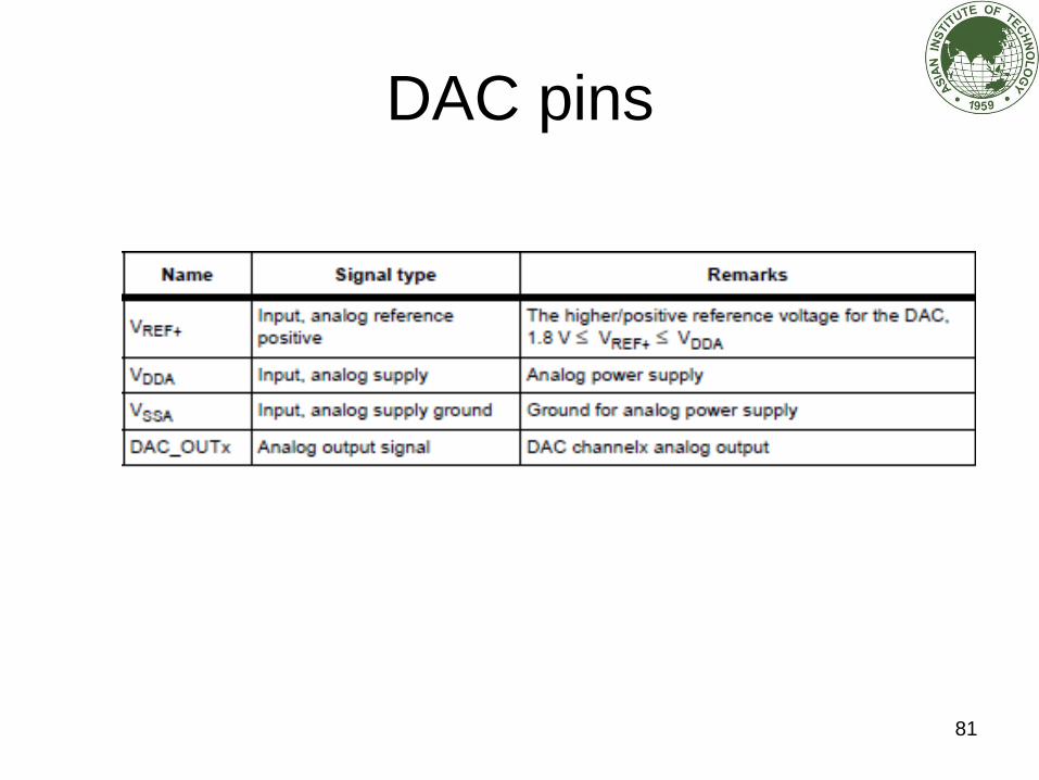
DAC pins
81

Simulink - DAC
• DAC block can be used to read data
82

Configurations
83

Configurations
• Digital to analog block to generate analog
signals (with the maximum of 2 channels)
– Channel1 = pin A4
– Channel2 = pin A5
• Analog output voltage = Vref x Data/ 4095
84

Example
85

Hardware Setup
86

Configuring
87

Configuring
88

Output
89

Question?
• Write a program to report error if the
analog reading ADC1 pin1 is lower than
10 or analog reading ADC2 pin 2 is higher
than 1000 using data align right.
90

Questions?
91