analog electronic circuits prof. shouribrata chatterjee ... · analog electronic circuits prof....
TRANSCRIPT
Analog Electronic CircuitsProf. Shouribrata Chatterjee
Department of Electrical EngineeringIndian Institute f Technology, Delhi
Lecture – 38Class D amplifiers, push-pull amplifiers
Welcome to Analogue Electronics. This is a lecture 38 and today we will continue from
the power amplifiers that we had discussed in the last class. So, in the last class we were
discussing class A, class B, class A B, class C power amplifiers, we had just about started
our discussion on class D power amplifiers. So, today our agenda is to cover class D
amplifiers and then push pull amplifiers which is another variation of power amplifiers
of class B power amplifiers ok. So, in the last class what we were doing so, our power
amplifier circuit is the same standard one.
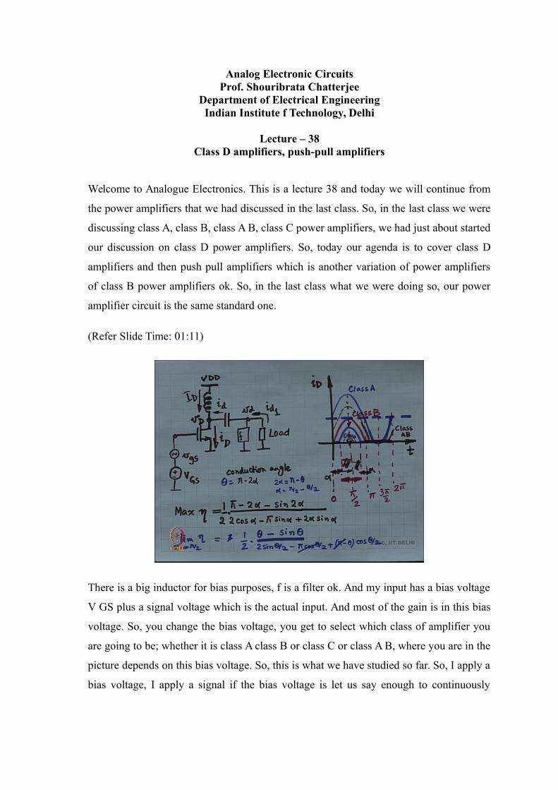
(Refer Slide Time: 01:11)
There is a big inductor for bias purposes, f is a filter ok. And my input has a bias voltage
V GS plus a signal voltage which is the actual input. And most of the gain is in this bias
voltage. So, you change the bias voltage, you get to select which class of amplifier you
are going to be; whether it is class A class B or class C or class A B, where you are in the
picture depends on this bias voltage. So, this is what we have studied so far. So, I apply a
bias voltage, I apply a signal if the bias voltage is let us say enough to continuously

conduct the MOSFET then, you are in a as a your working as a class A amplifier class A
power amplifier.
And we saw that the theoretical upper bound of the efficiency of a class A power
amplifier is 50 percent ok. So, the capacitor and the inductor are such that, you can split
the DC bias, the DC quantity of the voltage and the current from the signal quantity of
the voltage on the current ok. And this filter does a further splitting, the signal small i d is
filtered by this filter such that, only the fundamental component goes into the load, all
the other components go through the filter, so this is the arrangement. Now, what we do
is, if I start lowering the bias voltage then what happens is that the MOSFET is no longer
continuously conducting.
So, let us draw the picture. So, this is small i sub capital d as a function of time. And so
one possibility in class A the best case scenario is going up and down in this fashion this
is the best case scenario in class A right. In class B you cut off the negative half cycle all
together. Alright, so the conduction angle is just 180 degrees. In class C, so let me write
this down. So, in between class A and class B if you are somewhere in between then
what is that going to be called, it is going to be called class A B ok. So, that is the
conduction angle more than 180 degrees, but less than 360 degrees that is class A B.
Then you have got class B, where the conduction angle is 180 degrees. Then, I decrease
the conduction angle further and I get class C ok. So, here the conduction angle is less
than 180 degrees. Alright, and what we did in the last class was we came up with a
closed form expression actually, we said that lets say that the conduction angle is 2 times
alpha. So, we said let us say this angle is alpha ok. So, let us say that the MOSFET is
conducting from pi by 2 minus alpha to pi by 2 plus alpha in this region. Alright and we
came up with a closed form expression for the maximum efficiency of the power
amplifier. And we found that this was the maximum efficiency for example, if alpha is 0
so, I am sorry if alpha is yeah am I making a mistake.
Student: Sir that is the, not alpha (Refer Time: 08:16) 0 2.
So, this is what we have done in the last class ok. So, here the conduction angle is
actually pi minus 2 alpha is the total conduction angle. So for example, if alpha is equal
to 0 then you are actually boiling down to a class B situation so, you get pi minus 0. So,
pi in the numerator and 2 times cos of alpha that is 2 minus 0 plus a 0, so, there was a
half also. Please check the notes there was a half also factor in this. So, we had got a pi
by 4 as the efficiency when the conduction angle is pi; that is it is a class B circuit ok.
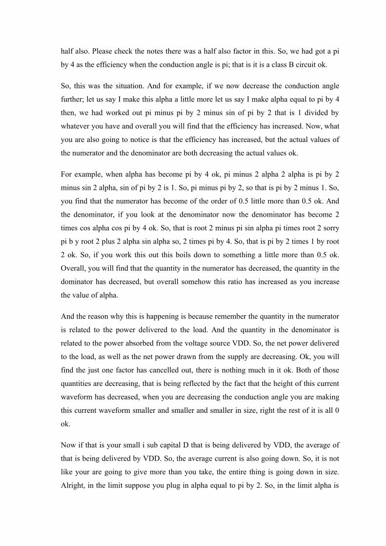
So, this was the situation. And for example, if we now decrease the conduction angle
further; let us say I make this alpha a little more let us say I make alpha equal to pi by 4
then, we had worked out pi minus pi by 2 minus sin of pi by 2 that is 1 divided by
whatever you have and overall you will find that the efficiency has increased. Now, what
you are also going to notice is that the efficiency has increased, but the actual values of
the numerator and the denominator are both decreasing the actual values ok.
For example, when alpha has become pi by 4 ok, pi minus 2 alpha 2 alpha is pi by 2
minus sin 2 alpha, sin of pi by 2 is 1. So, pi minus pi by 2, so that is pi by 2 minus 1. So,
you find that the numerator has become of the order of 0.5 little more than 0.5 ok. And
the denominator, if you look at the denominator now the denominator has become 2
times cos alpha cos pi by 4 ok. So, that is root 2 minus pi sin alpha pi times root 2 sorry
pi b y root 2 plus 2 alpha sin alpha so, 2 times pi by 4. So, that is pi by 2 times 1 by root
2 ok. So, if you work this out this boils down to something a little more than 0.5 ok.
Overall, you will find that the quantity in the numerator has decreased, the quantity in the
dominator has decreased, but overall somehow this ratio has increased as you increase
the value of alpha.
And the reason why this is happening is because remember the quantity in the numerator
is related to the power delivered to the load. And the quantity in the denominator is
related to the power absorbed from the voltage source VDD. So, the net power delivered
to the load, as well as the net power drawn from the supply are decreasing. Ok, you will
find the just one factor has cancelled out, there is nothing much in it ok. Both of those
quantities are decreasing, that is being reflected by the fact that the height of this current
waveform has decreased, when you are decreasing the conduction angle you are making
this current waveform smaller and smaller and smaller in size, right the rest of it is all 0
ok.
Now if that is your small i sub capital D that is being delivered by VDD, the average of
that is being delivered by VDD. So, the average current is also going down. So, it is not
like your are going to give more than you take, the entire thing is going down in size.
Alright, in the limit suppose you plug in alpha equal to pi by 2. So, in the limit alpha is
equal to pi by 2, so you say I am not going to conduct at all or I am just going to conduct
at this point, at this one point ok. What you going to find let us try it out if, alpha is equal
to pi by 2, how are you going to do it. You are going to plug in alpha equal to pi by 2, so
pi minus 2 times pi by 2 is 0 minus sin of pi is 0.
So, your numerator has become a big 0. Your denominator is 2 times cos of pi by 2, cos
of pi by 2 is a 0 minus pi times sin pi by 2, so that is minus pi plus 2 times pi by 2, which
is pi times sin pi by 2 so, that is also 1. So, minus pi plus pi which is 0, so your
numerator is 0 denominator is 0 ok. So, you have got a 0 by 0 situation and therefore, we
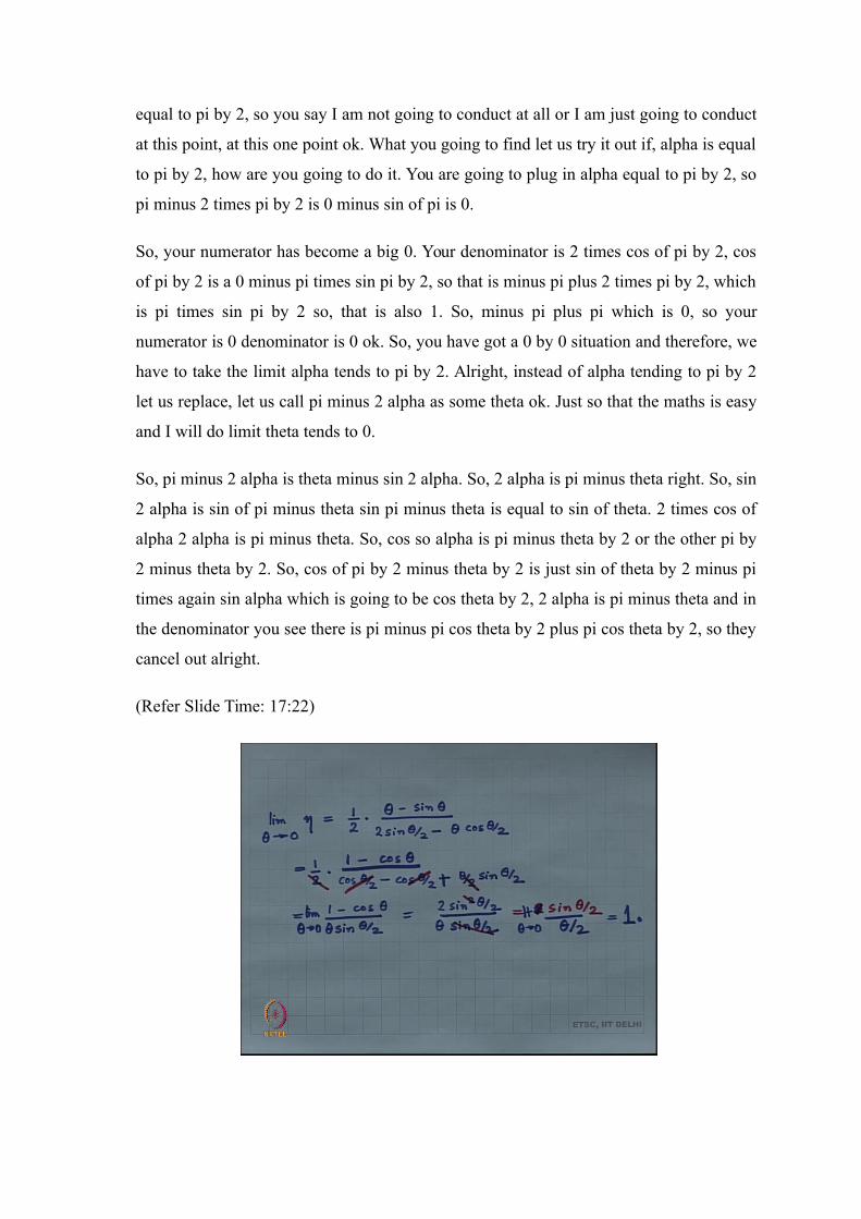
have to take the limit alpha tends to pi by 2. Alright, instead of alpha tending to pi by 2
let us replace, let us call pi minus 2 alpha as some theta ok. Just so that the maths is easy
and I will do limit theta tends to 0.
So, pi minus 2 alpha is theta minus sin 2 alpha. So, 2 alpha is pi minus theta right. So, sin
2 alpha is sin of pi minus theta sin pi minus theta is equal to sin of theta. 2 times cos of
alpha 2 alpha is pi minus theta. So, cos so alpha is pi minus theta by 2 or the other pi by
2 minus theta by 2. So, cos of pi by 2 minus theta by 2 is just sin of theta by 2 minus pi
times again sin alpha which is going to be cos theta by 2, 2 alpha is pi minus theta and in
the denominator you see there is pi minus pi cos theta by 2 plus pi cos theta by 2, so they
cancel out alright.
(Refer Slide Time: 17:22)

And then you get, you can double check, if you plug in theta equal to 0 this is 0 0 0 0 so,
you still have 0 by 0 and then we will do a limit. How do you do a limit when there is a 0
by 0, you take the derivative right of both numerator and denominator your L'Hospital's
rule. So, you take the derivative of the numerator, you get 1 minus cos theta divided by 2
times sin theta by 2 derivative is half cos theta by 2. And theta cos theta by 2 you have to
break it up and these cos theta by 2 is cancel out, this by 2 also cancels out. And you
again plug in theta equal to 0 and you see that you have still got a 0 by 0, which is still
not good enough, so you do the derivative again perfect. So, one possibility is instead of
doing a derivative again, you suggest that 1 minus cos theta is equal to 2 times sin square
theta by 2. There is a half which is disappeared mysteriously ok.
So, this sin theta by 2 cancels out yeah it is fine, no there was a theta here, yeah that is
right it is correct, we are still doing limit theta tends to 0 and then it is sin theta by 2 by
theta by 2, which is equal to 1. So, what do you see over here, you see that as you are
dropping the conduction angle all the way to 0, it is as if the efficiency is building up
higher and higher and higher all the way to 1. Although in reality as your dropping the
conduction angle to 0, you are not doing anything, you are barely supplying any current
and barely pushing that current into the load, but whatever you are doing it is very good
it is 100 percent efficient ok. So, this limiting case of the amplifier is called a class D
amplifier ok where you are conduction angle drops all the way to 0.
(Refer Slide Time: 22:01)

Now, what does that mean; that means that the MOSFET barely ever switches on and
when it done switch on ok, so this is our circuit ok. Now, considered the following
situation, consider this MOSFET to be a very good MOSFET, very large in size and it is
going to operate as a perfect switch. What does a switch do, a switch is either on or off
ok. When the switch is on these two voltages are equal. Therefore, the power consumed
by the MOSFET, when the switch is on is equal to 0 because, these two voltages are
equal ok. Power consumed by the MOSFET is the voltage times the current, right power
consumed by the MOSFET is V D times i D, when the switch is on V D is equal to 0, the
MOSFET does not get to consume any power.
When the switch is off, i d is 0 because, the switch is off in which case again the
MOSFET does not get to consume any power. So, if I can operate the MOSFET as a
switch then the MOSFET does not consume any power at all. Which means, whatever
comes from the power supply makes its way to the load, the power that the power supply
produces can only be delivered to the load because, nothing else consumes any power
ok. So, this is the understanding, this is the class D amplifier. In the class D amplifier
what you are going to do is you are going to operate this MOSFET as a switch.
You think nothing is going to happen over here ok, you think you are not going to do
anything, the MOSFET is not doing anything, but no you are wrong wait a second ok.
What you are going to do is this voltage, what you going to do is you are going to make
sure that the signal is enough to switch the device either on or off and the MOSFET is
not going to behave like an amplifier at all. This device is so large, so great and the input
amplitude is so large, so strong that the MOSFET is going to work like a switch. When it
is on immediately VD is going to become equal to 0 ok. So, all the current will get
delivered to the load. When it is off i D is equal to 0, which means all the power will get
delivered to the load ok.
So, this is a classic class D amplifier; class D amplifiers are very hard to make right, the
theoretical efficiency of the class D amplifier is 100 percent. However, in a lot of audio
systems, a lot of audio systems we find that the class D amplifier is quite popular
because of its efficiency. So, what you do is at the input over here instead of applying the
actual audio signal right, the audio signal look like this, something instead of applying
this audio signal, you encode this audio signal as a pulse width modulated waveform ok.
A very fast this audio signal has a bandwidth of 20 kilo hertz maximum bandwidth
including music right, high quality music the human audio signal has a range of 20 kilo
hertz, some 20 hertz to 20 kilo hertz ok.
Now, what we do is instead of just a 20 kilo hertz bandwidth, you say that lets take a 1
mega hertz bandwidth alright. And in this 1 mega hertz bandwidth, you convert this 20
kilo hertz signal into a pulse width modulated waveform. What is pulse, what is pulse
width modulation, what is it? Here the it is a square wave, where the width of the pulse is
proportional to the signal amplitude ok. Suppose, the signal amplitude is this much then I
produce this, suppose the signal amplitude is this much, I produce this ok, this pulse. And
these pulses are coming fast right much faster than the bandwidth of the signal ok.
So, the bandwidth of this particular signal is much much larger than the bandwidth of the
original signal, the original signal is just 20 kilo hertz, this one is very high bandwidth
and it is a switching waveform. Now we apply the switching waveform over here right.
The current the MOSFET is switching on and off this is a digital signal. Alright this is a
pure digital signal the MOSFET is just switching on off on off, when it is on VD is 0.
MOSFET does not consume any power. Power is delivered to the load. When it is off,
current is 0, once again power is delivered to the load; no matter what you do, power is
delivered only to the load and nowhere else alright.
Applications such as the hearing aid dumb they do not even put the filter over here, lot of
hearing aid applications. They do not even bother putting a filter over here why because,
they say that the human ear is a good enough filter right. Anyway, the human ear has a
range of 20 kilo hertz right, all the harmonics outside of 20 kilo hertz is going to filter it
out anyway right. Of course, this leads to a lot of distortion because, if the signal was not
20 kilo hertz, if the signal was 1 kilo hertz then, all its harmonics are there right 3 kilo
hertz, 5 kilo hertz, 2 kilo hertz all the harmonics are there, if the signal is 1 kilo hertz, but
the hearing aid engineer said that that guy the patient was not able to hear anything, let
him hear at least distorted signal it is ok.
Right at this price this is what I am going to give him, he eliminates the filter all together.
Ok then, a lot of other applications what they do is they say that the load is inductive in
an audio speaker, the loudspeaker right, the speaker itself is an inductor. So, you form
and L c filter over here right away. And you engineer the L c values such that, you get the
right filtering ok, this is also something that a lot of engineers do. So, they eliminate this
filter altogether alright. So, thus audio speaker is can be modeled as an inductor in series
with the resistor, right it is not a pure resistor in which case you have got L c r in series.
Now, you play with the c value and you make sure that it is a nice filter and cuts out all
the signals that you do not want ok. You could also remodel this as L in shunt with r
right, so lot of possibilities are there. In fact, that would be a more natural model right, L
in shunt with r will be a more physical model then L in series with r anyway. So, you
play around with these values and you can actually it is possible to eliminate the filter
altogether. Hi fi applications will actually put a filter over here right, let us say you have
got a hi fi high fatality audio application, let us say you pay a lot of money and buy nice
stereo player right, they are going to actually implement a real filter over there and make
sure that the output sound is clean.
However, a lot of these systems come like this ok. There are a few exceptions, the
exceptions being car audio amplifiers ok. Car audio amplifiers, audio amplifiers that you
used in the car, your radio car, radio speaker right, there you do not use this. And the
reason is that this generates a lot of harmonics right, things are very different in the car.
There is a lot of electromagnetic emission inside the car and that is going to create a lot
of problems right. You do not want for example, this audio amplifier to start it interfering
with the engine control ok.
So, lot of critical things are there and as a result in applications like a car, you are going
to stick to cleaners amplifiers which are class A and class B are best not class D. Because
class D is called is known as a switching amplifier alright. So, these power amplifiers
can be classified into two broad classes.
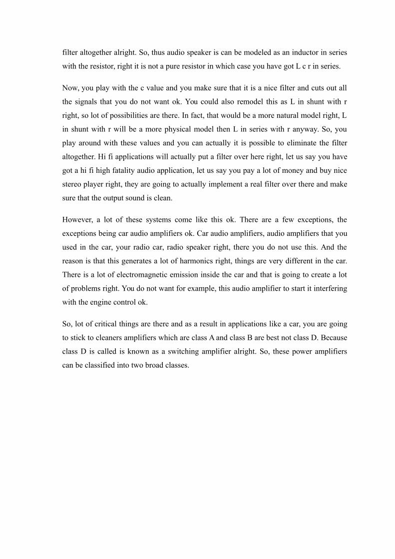
(Refer Slide Time: 33:06)
One class is the linear power amplifier, the other class is the switching power amplifier
ok, where the device is being used as a switch. So the switching power amplifier is class
D, the linear power amplifier ok. This linear take it with a pinch of salt alright, the circuit
is not a linear circuit as such, however the amplitude of the signal varies with the
amplitude, the amplitude of the output power, the output power changes with the input
amplitude ok.
So, these are called linear power amplifiers. A switching power amplifier is class D and
then there are a few more they are called class E and class F ok. So, they all are variants
of class D power amplifiers, we are not going to study them. Fine efficiency in class A is
50 percent, class B is 78 percent theoretical maximum, class C is greater than 78 percent,
class A B is between 50 and less than 78, these the theoretical maximums and class D E
F they are all switching their theoretical maximum is a cool 100 percent ok. But then
again these are all theoretical maximums, you never really going to hit these values.
For example, if you start designing a class A amplifier, then you are never going to
achieve 50 percent, your supervisor, your boss will be happy if you hit 25 ok. You start
designing a class C amplifier, you are never going to hit 78 percent you know anything
greater than 78 percent, it will be nice if you can manage 70 percent. You start designing
a class D D class D E F’s are very very hard to design, but you start designing them. Let
us say you start designing a class C amplifier right, your target is 10 percent, but you will
never reach anywhere close by, you will probably be somewhere around 70 75 percent
you should be happy ok.
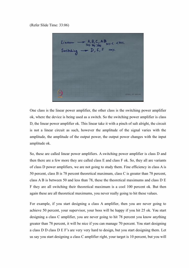
So, these are the different power amplifiers right and they are all what is the circuit, the
circuit is the same this one right, there is nothing different. It is the same circuit, you are
just playing with the VGS value and in case of the switching amplifiers you know, you
change the input signal as well, you make it a pulse width modulator nice huge digital
signal right, you make the MOSFET big in case of a class D E F amplifier right, but
otherwise the basic circuit is the same. The idea is how to split up the current waveform
the voltage waveform how to take out the fundamental that is where everything is ok.
(Refer Slide Time: 36:45)
Now, we are going to do one more, one last power amplifier and so let us think about
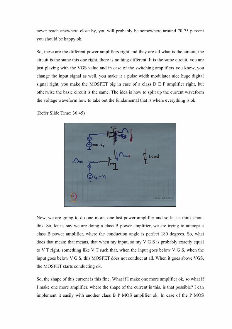
this. So, let us say we are doing a class B power amplifier, we are trying to attempt a
class B power amplifier, where the conduction angle is perfect 180 degrees. So, what
does that mean; that means, that when my input, so my V G S is probably exactly equal
to V T right, something like V T such that, when the input goes below V G S, when the
input goes below V G S, this MOSFET does not conduct at all. When it goes above VGS,
the MOSFET starts conducting ok.
So, the shape of this current is this fine. What if I make one more amplifier ok, so what if
I make one more amplifier, where the shape of the current is this, is that possible? I can
implement it easily with another class B P MOS amplifier ok. In case of the P MOS

amplifier, what do I have to do, I have to make sure that this voltage the bias voltage is
exactly VDD minus V T such that, when V G S the input signal goes up, this one blocks
out everything, but when it goes down it pushes current or rather it draws current the
other way right when it goes down yeah ok.
So, this current waveform. If this is equal to 0 the current is 0. If the signal is 0, there is
no current. If the signal goes down, there is no current sorry, if the signal goes up there is
no current, but when the signal goes down, I am sorry these arrows are wrong. When the
signal goes down, the current that is being pushed goes up fine, all of these references
are 0. That is the current that is being pushed. Alright is this so far so, the same signal is
being applied to both of these transistors both of these MOSFETs. So, let us redraw.
(Refer Slide Time: 41:00)
So, here I am applying something like this and this current has a conduction angle of 180
degrees, the other current also has a conduction angle of 180 degrees fine. And then I
hook them up ok, if I hook them up and make sure that the current drawn from VDD is a
constant. Suppose the DC current ok, if you look them up what is this other current, this
1 minus, this minus the other current ok. And this particular current is therefore, going to
be in this phase it tracks the first one fine.
So, what I am doing is I am calling this i D N, i D P and i d is equal to i D N minus i D P
alright. And what I do is, I am going to put this across my load alright. When I do that, I
get both of these MOSFETs are operating with a conduction angle of 180 degrees pi, pi
is the conduction angle, both of them are class B ok, both of the MOSFETs are operating
in class B, is that ok. The resulting current is coming through the load. So, one P MOS is
pushing current into the load the other N MOS is pulling current out of the load.
So, this kind of strategy is called a push pull class B power amplifier. The efficiency of
this power amplifier is exactly the same as that of the original class B. All that you have
done is you have replaced the inductor with the PMOS right and for the PMOS you have
replaced the inductor with a NMOS ok. And then you have to organize these bias
voltages. These bias voltages are critical ok. You have to organize this to be perfect such
that the P MOS is class B, you have to organize this as perfect such that the NMOS is in
class B. Once you have organized the biased voltages, everything is going to fall into
place. Now, how you are going to do, this is actually your own business alright, it
actually is your own business right, one possibility would be that you somehow generate
this ok, somehow and then couple the input signal in ok.
You can do this through a resistive network, you can do it through other, but you have to
be perfect. It has this has to be something like V T right, maybe you can do it through
another MOSFET right, which emulates a V T voltage right this should emulate a PMOS
V T voltage right, you can do a number of things to do that. For example, you could have
a current source, which is drawing current from VDD right and it gives you a V T drop
over. So, this part is your business, as long as you do this part right this is going to push,
this is going to pull. You can even make this as common drain, as a post to commons
source. Actually the common drain is also very popular.
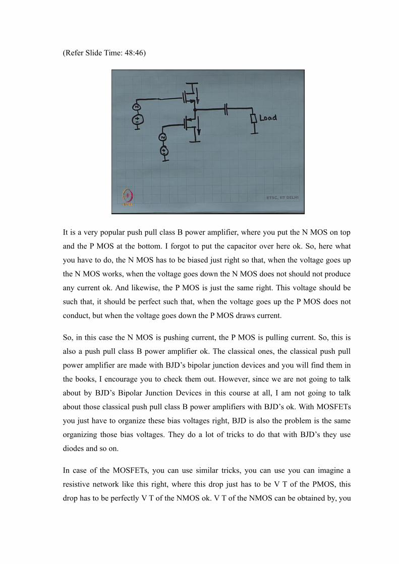
(Refer Slide Time: 48:46)
It is a very popular push pull class B power amplifier, where you put the N MOS on top
and the P MOS at the bottom. I forgot to put the capacitor over here ok. So, here what
you have to do, the N MOS has to be biased just right so that, when the voltage goes up
the N MOS works, when the voltage goes down the N MOS does not should not produce
any current ok. And likewise, the P MOS is just the same right. This voltage should be
such that, it should be perfect such that, when the voltage goes up the P MOS does not
conduct, but when the voltage goes down the P MOS draws current.
So, in this case the N MOS is pushing current, the P MOS is pulling current. So, this is
also a push pull class B power amplifier ok. The classical ones, the classical push pull
power amplifier are made with BJD’s bipolar junction devices and you will find them in
the books, I encourage you to check them out. However, since we are not going to talk
about by BJD’s Bipolar Junction Devices in this course at all, I am not going to talk
about those classical push pull class B power amplifiers with BJD’s ok. With MOSFETs
you just have to organize these bias voltages right, BJD is also the problem is the same
organizing those bias voltages. They do a lot of tricks to do that with BJD’s they use
diodes and so on.
In case of the MOSFETs, you can use similar tricks, you can use you can imagine a
resistive network like this right, where this drop just has to be V T of the PMOS, this
drop has to be perfectly V T of the NMOS ok. V T of the NMOS can be obtained by, you
can obtain a V T of the N MOS by pushing a small current through a large N channel
MOSFET. If I push a small current through a large N channel MOSFET right, V G S t
required for this MOSFET is going to be very low, which means that this is just going to
be enough, it is just going to be VT right.
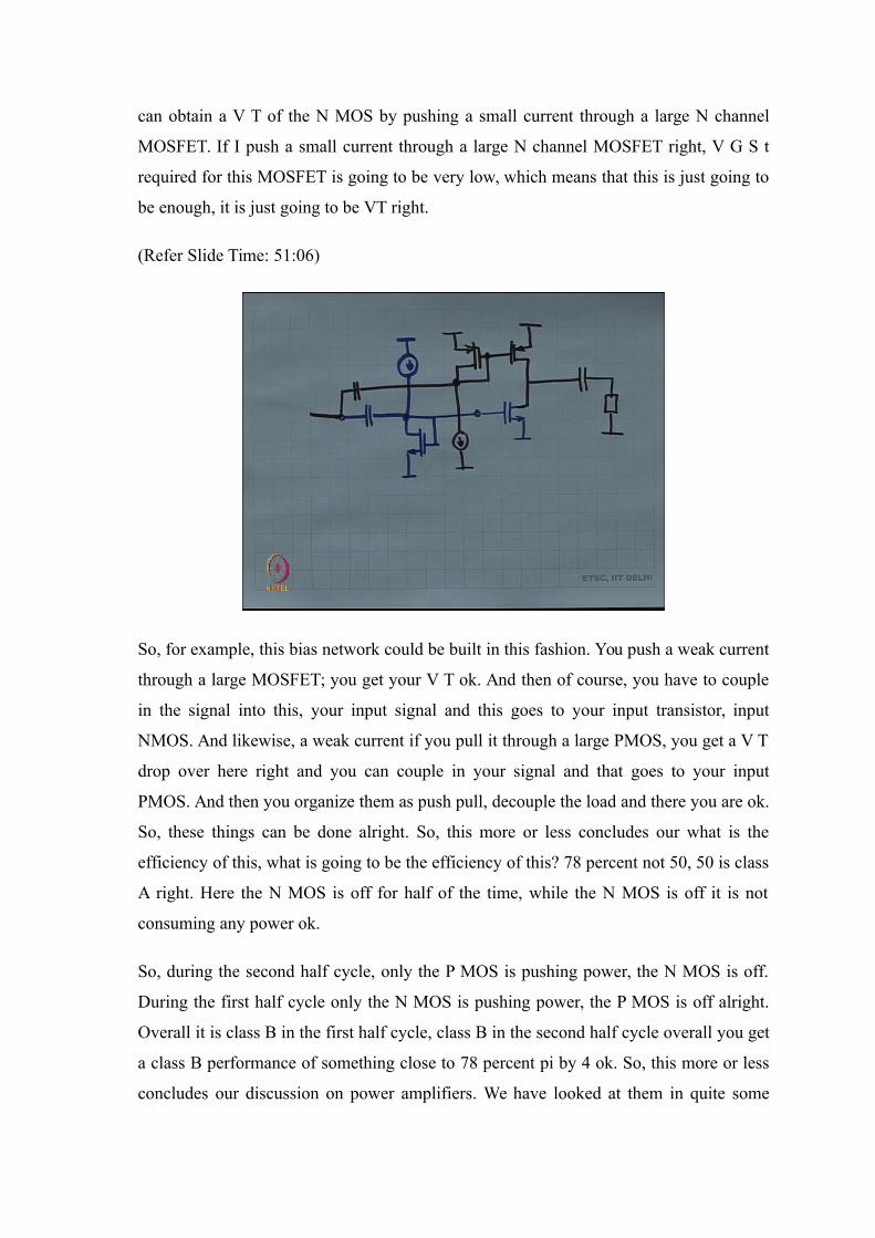
(Refer Slide Time: 51:06)
So, for example, this bias network could be built in this fashion. You push a weak current
through a large MOSFET; you get your V T ok. And then of course, you have to couple
in the signal into this, your input signal and this goes to your input transistor, input
NMOS. And likewise, a weak current if you pull it through a large PMOS, you get a V T
drop over here right and you can couple in your signal and that goes to your input
PMOS. And then you organize them as push pull, decouple the load and there you are ok.
So, these things can be done alright. So, this more or less concludes our what is the
efficiency of this, what is going to be the efficiency of this? 78 percent not 50, 50 is class
A right. Here the N MOS is off for half of the time, while the N MOS is off it is not
consuming any power ok.
So, during the second half cycle, only the P MOS is pushing power, the N MOS is off.
During the first half cycle only the N MOS is pushing power, the P MOS is off alright.
Overall it is class B in the first half cycle, class B in the second half cycle overall you get
a class B performance of something close to 78 percent pi by 4 ok. So, this more or less
concludes our discussion on power amplifiers. We have looked at them in quite some

detail right, we have not done enough to actually make real R F power amplifiers for cell
phones, but we have done quite a bit right. We have covered the basics of power
amplifiers both in terms of audio power amplifier as well in terms of cell phone power
amplifiers, which are going to drive an antenna. So, both of those we have covered.
And next we are going to look at voltage regulators in the next class.
Thank you.