analog and telecommunication electronics - polito.it · atlce - c6 20/03/2016 © 2016 ddc 2 page 2...
TRANSCRIPT
ATLCE - C6 20/03/2016
© 2016 DDC 1Page 1
20/03/2016 - 1 ATLCE - C6 - © 2016 DDC
Analog and Telecommunication Electronics
C6 - Signal synthesizers
» Integer/Fractional synthesizer» Direct digital synthesis (DDS) » Integrated PLL type 4046» Digital PLL
AY 2015-16
Politecnico di TorinoElectronic Eng. Master Degree

ATLCE - C6 20/03/2016
© 2016 DDC 2Page 2
20/03/2016 - 2 ATLCE - C6 - © 2016 DDC
Lesson C6: signal synthesizers
• Analog VCO circuits
• Frequency synthesizers– Integer and fractional synthesizers
• Direct digital synthesis (DDS and NCO)– Structures and parameters– DDS for FM, PM, AM
• Examples of integrated PLL – The 4046 family
• References– D. Del Corso: Elettronica per Telecomunicazioni: 3.7– S. Franco: Design with OA and Analog IC: 13.5

ATLCE - C6 20/03/2016
© 2016 DDC 3Page 3
20/03/2016 - 3 ATLCE - C6 - © 2016 DDC
VCO taxonomy
• Limited frequency change: < or– Low frequency (k 10 MHz)
» V-C or I-C circuits
– High frequency: LC circuits
• Wide frequency change: ≈ or– Low frequency (k 10 MHz)
» V-C or I-C circuits
– High frequency: LC circuits with beat
ωor ω0
Δωor
ωor ω0
Δωor

ATLCE - C6 20/03/2016
© 2016 DDC 4Page 4
20/03/2016 - 4 ATLCE - C6 - © 2016 DDC
I-C VCO
• Use Op.Amp., SW, analog components– Exponential (RC) or linear (constant current) charge/discharge
of a capacitor– Comparison with thresholds Vt for char/discharge switching
• Fixed threshold, variable charging current– I depends on VCO control voltage Vc– As Vc reaches Vt, current (or capacitor) is inverted– High current dynamics wide frequency change
• Fixed charging current, variable thresholds– Vt depends on VCO control voltage Vc– As Vc reaches Vt, current (or capacitor) is inverted– Low voltage dynamics (noise!) small frequency change

ATLCE - C6 20/03/2016
© 2016 DDC 5Page 5
20/03/2016 - 5 ATLCE - C6 - © 2016 DDC
I-C VCO, variable current
• Linear charge (current mirror S), I(VC), C inversion– As VA reaches the T1 threshold SWA-B toggle; I is inverted,
VA = 0; VB becomes negative and continues to raise– As VB reaches the T2 threshold SWA-B toggle; I is inverted
VB = 0; VA becomes negative and continues to raise …
VB
SWB
VA
ISWA
R1
R2 I
Vdd
VC
SWA
VO

ATLCE - C6 20/03/2016
© 2016 DDC 6Page 6
20/03/2016 - 6 ATLCE - C6 - © 2016 DDC
I-C VCO, variable threshold
• Exp charge (RC), current inversion, Vt(Vc)– Vti depends on control voltage Vc (voltage divider R1, R2)– As Vc reaches Vt1, Vo = 0, capacitor starts discharging– As Vc reaches Vt2, Vo = Val, capacitor starts charging
Vt1
Vt2
VCO in NE567 (lesson B5)
VC
VO

ATLCE - C6 20/03/2016
© 2016 DDC 7Page 7
20/03/2016 - 7 ATLCE - C6 - © 2016 DDC
VCO with tuned circuit
• Tuned circuit: ωO = SQRT(1/LC)
• Modified with changing C– Varactor diode
• Small frequency change– Direct LC VCO
• Wide frequency change– Beat with fixed referenceO = OR - OC
fixed variable
ATLCE - C6 20/03/2016
© 2016 DDC 8Page 8
20/03/2016 - 8 ATLCE - C6 - © 2016 DDC
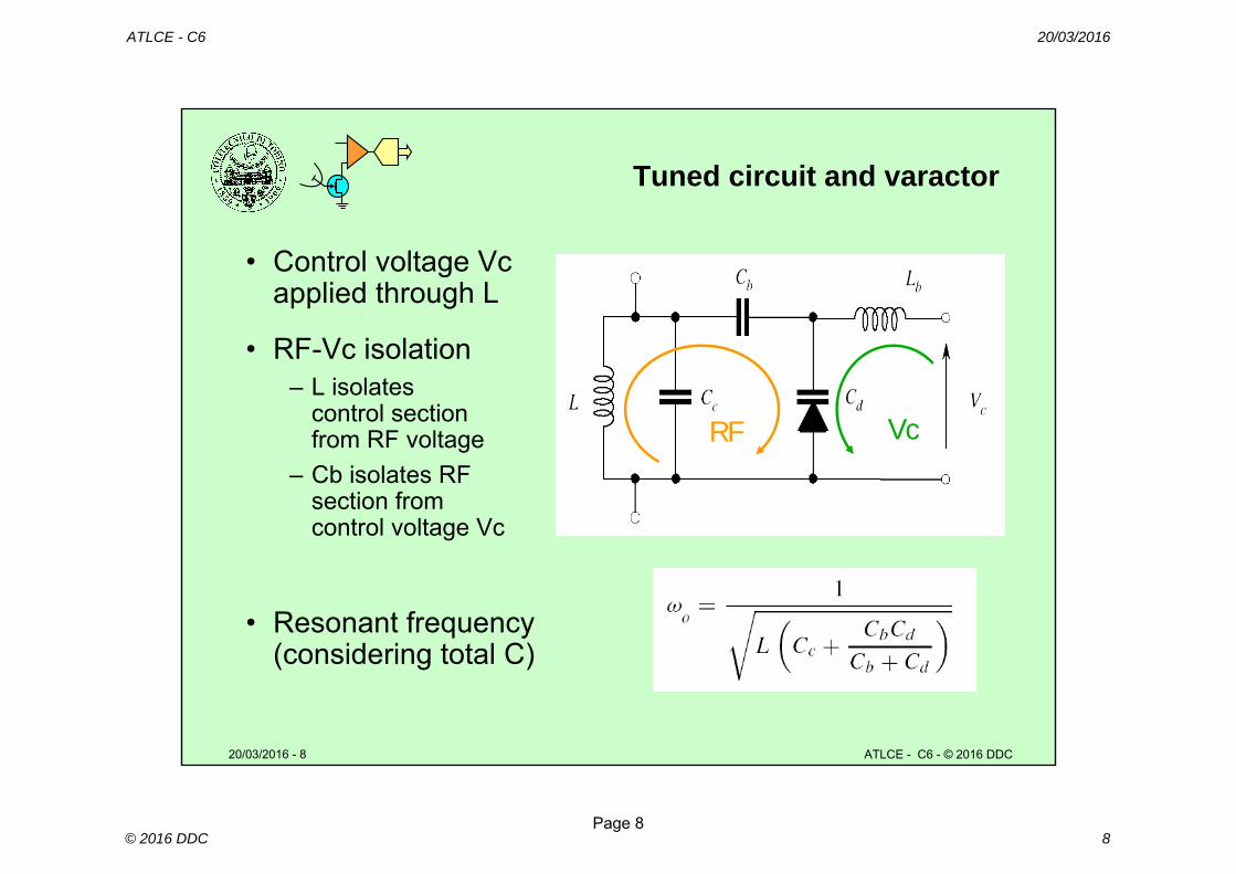
Tuned circuit and varactor
• Control voltage Vcapplied through L
• RF-Vc isolation– L isolates
control section from RF voltage
– Cb isolates RFsection from control voltage Vc
• Resonant frequency (considering total C)
RF Vc

ATLCE - C6 20/03/2016
© 2016 DDC 9Page 9
20/03/2016 - 9 ATLCE - C6 - © 2016 DDC
Phase noise and spurs
• With steady Vc the VCO generates pure signals
• Changes of Vc cause phase and frequency variations
• Noise and random changes– Phase noise– Wider Vo spectrum
• Periodic changes – new spectral lines – spurious
(carrier FM)
f
ffo
ATLCE - C6 20/03/2016
© 2016 DDC 10Page 10
20/03/2016 - 10 ATLCE - C6 - © 2016 DDC
Lesson C6: signal synthesizers
• Analog VCO circuits
• Frequency synthesizers– Integer synthesizers– Settling time – Fractional synthesizers
• Direct digital synthesis (DDS and NCO)– Structures and parameters– DDS for FM, PM, AM
• Examples of integrated PLL – The 4046 family

ATLCE - C6 20/03/2016
© 2016 DDC 11Page 11
20/03/2016 - 11 ATLCE - C6 - © 2016 DDC
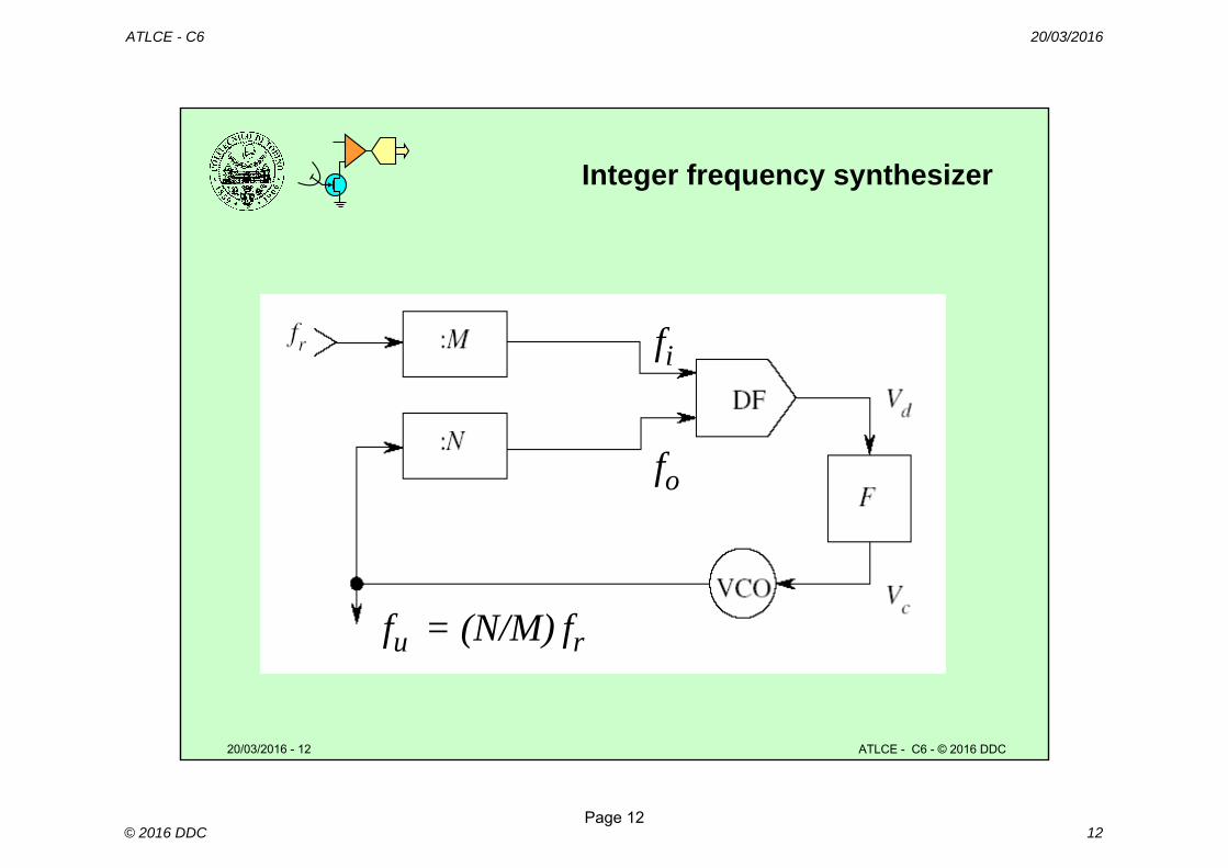
Frequency synthesizers
• Input: reference signal, frequency Fr
• Divide by N counter between VCO (Fu) and PD– Fi = Fr; Fu/N = Fo;– Output frequency Fu = N Fr
• Divide by M counter on the input (Fr)– Fi = Fr/M; Fu/N = Fr/M;– Output frequency Fu = N/M Fr
• Unique reference Fr for any output frequency – Precision signal generators– Digital tuning (synthesized LO)
ATLCE - C6 20/03/2016
© 2016 DDC 12Page 12
20/03/2016 - 12 ATLCE - C6 - © 2016 DDC
Integer frequency synthesizer
fi
fu = (N/M) fr
fo

ATLCE - C6 20/03/2016
© 2016 DDC 13Page 13
20/03/2016 - 13 ATLCE - C6 - © 2016 DDC
Settling time and resolution
• Settling time depends on F(s) and required precision– F(s): lowpass filter, cutoff about Fi /10
• Resolution: For N N+1, Fu Fu + Fo– Minimum frequency step: Fo = Fi = Fr/M
• High resolution low Fi, Fo some drawbacks:– Low cutoff in F(s)– Slow transient response– Long settling time
• Speed up the transient response– Higher Fi and Fo higher cutoff in F(s)– Increased channel spacing
ATLCE - C6 20/03/2016
© 2016 DDC 14Page 14
20/03/2016 - 14 ATLCE - C6 - © 2016 DDC
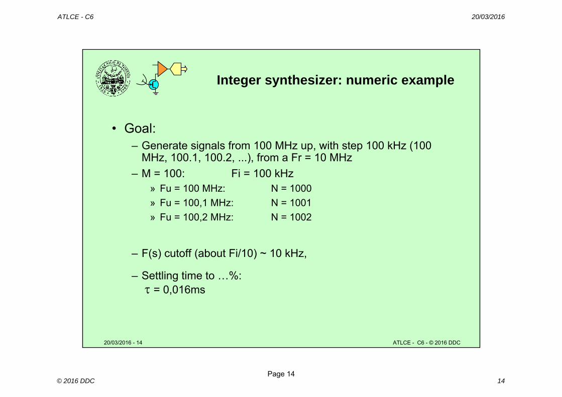
Integer synthesizer: numeric example
• Goal:– Generate signals from 100 MHz up, with step 100 kHz (100
MHz, 100.1, 100.2, ...), from a Fr = 10 MHz– M = 100: Fi = 100 kHz
» Fu = 100 MHz: N = 1000 » Fu = 100,1 MHz: N = 1001 » Fu = 100,2 MHz: N = 1002
– F(s) cutoff (about Fi/10) ~ 10 kHz,
– Settling time to …%: = 0,016ms

ATLCE - C6 20/03/2016
© 2016 DDC 15Page 15
20/03/2016 - 15 ATLCE - C6 - © 2016 DDC
Fractional synthesizer
• Conflicting parameters: high resolution, fast settling– high M and N low Fi and Fo low frequency F(s) pole slow response
• Keep N, M low divide by not-integer M, N numbers – Higher Fi, Fo– Higher cutoff for F(s)– Faster response
• Fractional synthesizer– Periodic change of the divide factor (N N+1)
» Actual divide ratio related with cycling duty cycle» Residual FM phase noise
• Known, can be corrected

ATLCE - C6 20/03/2016
© 2016 DDC 16Page 16
20/03/2016 - 16 ATLCE - C6 - © 2016 DDC
Example of fractional synthesizer
Divider ratio changes with duty cycle D
D divide by N1-D divide by N+1
Fu = Fo*N*(N+1)/(D+N)
fi
fo
fu
Average Fo = D(Fu/N) + (1-D)Fu/(N+1)
Equivalent divider ratio: N*(N+1)/(D+N)
ATLCE - C6 20/03/2016
© 2016 DDC 17Page 17
20/03/2016 - 17 ATLCE - C6 - © 2016 DDC
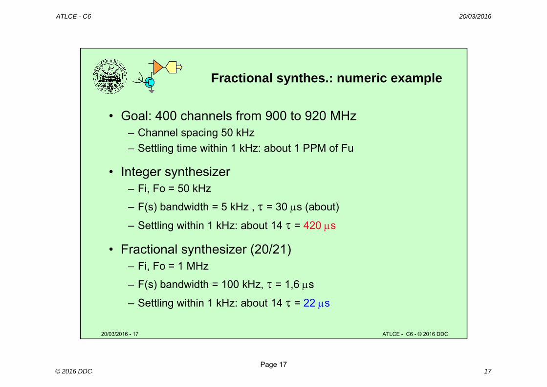
Fractional synthes.: numeric example
• Goal: 400 channels from 900 to 920 MHz– Channel spacing 50 kHz– Settling time within 1 kHz: about 1 PPM of Fu
• Integer synthesizer– Fi, Fo = 50 kHz
– F(s) bandwidth = 5 kHz , = 30 s (about)
– Settling within 1 kHz: about 14 = 420 s
• Fractional synthesizer (20/21)– Fi, Fo = 1 MHz
– F(s) bandwidth = 100 kHz, = 1,6 s
– Settling within 1 kHz: about 14 = 22 s
ATLCE - C6 20/03/2016
© 2016 DDC 18Page 18
20/03/2016 - 18 ATLCE - C6 - © 2016 DDC
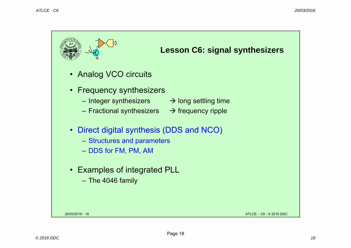
Lesson C6: signal synthesizers
• Analog VCO circuits
• Frequency synthesizers– Integer synthesizers long settling time – Fractional synthesizers frequency ripple
• Direct digital synthesis (DDS and NCO)– Structures and parameters– DDS for FM, PM, AM
• Examples of integrated PLL – The 4046 family

ATLCE - C6 20/03/2016
© 2016 DDC 19Page 19
20/03/2016 - 19 ATLCE - C6 - © 2016 DDC
Direct Digital Synthesis: DDS
• Table with signal samples– ROM, RAM filled by HW or SW algorithms
• Cyclic table scanning– Frequency change by changing
» Scan rate» Scan step
– In DDS: fixed scan rate, variable step– Analog output signal from DAC
• Pointer to samples generated by an adder– Next pointer = current pointer + scan step
• Simple example: sawtooth generator

ATLCE - C6 20/03/2016
© 2016 DDC 20Page 20
20/03/2016 - 20 ATLCE - C6 - © 2016 DDC
Basic DDS block diagram
PHASE ACCUMULATOR
SAMPLETABLE
LOWPASS
FILTERDAC
Pointer to samples
Removes harmonics caused by sampling
Δφ
Phase step (sample-to-sample phase difference)
Digital value of samples
Analog samples

ATLCE - C6 20/03/2016
© 2016 DDC 21Page 21
20/03/2016 - 21 ATLCE - C6 - © 2016 DDC
Direct digital synthesis - a
• Sawtooth signal– Full table (signal for step 1)– 0, 1, 2, 3, 4, 5, ... 9

ATLCE - C6 20/03/2016
© 2016 DDC 22Page 22
20/03/2016 - 22 ATLCE - C6 - © 2016 DDC
Direct digital synthesis - b
• Sawtooth signal– Full table (signal for step 1)– 0, 1, 2, 3, 4, 5, 6, 7, 8, 9, 0
– Samples for step 2– 0, 2, 4, 6, 8, 0, 2, 4, 6, ...

ATLCE - C6 20/03/2016
© 2016 DDC 23Page 23
20/03/2016 - 23 ATLCE - C6 - © 2016 DDC
Direct digital synthesis - c
• Sawtooth signal– Full table (signal for step 1)– 0, 1, 2, 3, 4, 5, 6, 7, 8, 9, 0
– Samples for step 2– 0, 2, 4, 6, 8, 0, 2, 4, 6, ...
– Samples for step 3– 0, 3, 6, 9, 2, 5, 8, 1, 4, ...
– Samples for step 4– 0, 4, 8, 2, 6, 0, 4, 8, 2, ...

ATLCE - C6 20/03/2016
© 2016 DDC 24Page 24
20/03/2016 - 24 ATLCE - C6 - © 2016 DDC
Example of DDS operation
• LUT with 100 samples (K = 100, full period)
• Scan rate Fs = 1 Ms/s; scan period Ts = 1μs– Step S = 1; Full scan in N=100 steps;
To = 100 μs; Fo= 10 kHz
• Output signal frequency: Fo = Fs*N/K
130 kHz7,96 μs7,9613
250 kHz4 μs425
20 kHz50 μs502
10 kHz100 μs1001
Output freq. Fo=1/To
Scan periodTo=N*Ts
Num of stepsN=K/S
Scanstep S

ATLCE - C6 20/03/2016
© 2016 DDC 25Page 25
20/03/2016 - 25 ATLCE - C6 - © 2016 DDC
Direct digital synthesis
• Can be used for any signal shape– Time compression– Not frequency translation
• Used in wavetable sound boards
• No transient in frequency change– No loop to settle
• No transient for phase jump
• Allows direct generation of FM and PM signals

ATLCE - C6 20/03/2016
© 2016 DDC 26Page 26
20/03/2016 - 26 ATLCE - C6 - © 2016 DDC
Complete DDS block diagram
PHASE ACCUMULATOR
SINETABLE
LOWPASS
FILTERDAC
Or any other waveform
Removes harmonics caused by sampling
Δφ
ATLCE - C6 20/03/2016
© 2016 DDC 27Page 27
20/03/2016 - 27 ATLCE - C6 - © 2016 DDC
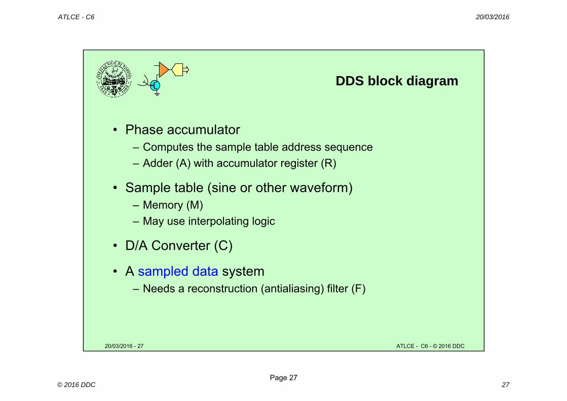
DDS block diagram
• Phase accumulator– Computes the sample table address sequence– Adder (A) with accumulator register (R)
• Sample table (sine or other waveform)– Memory (M)– May use interpolating logic
• D/A Converter (C)
• A sampled data system– Needs a reconstruction (antialiasing) filter (F)

ATLCE - C6 20/03/2016
© 2016 DDC 28Page 28
20/03/2016 - 28 ATLCE - C6 - © 2016 DDC
Modulation with DDS
• Direct modulation achieved by changing numeric parameters
• FM– Modify the scan step
• PM– Add a constant to phase accumulator during the scan
• AM– Multiply wavetable output samples – PAM/ASK: amplitude steps as power of 2 bit shift

ATLCE - C6 20/03/2016
© 2016 DDC 29Page 29
20/03/2016 - 29 ATLCE - C6 - © 2016 DDC
FM with DDS
• Modify the scan step
Frequencymodulation

ATLCE - C6 20/03/2016
© 2016 DDC 30Page 30
20/03/2016 - 30 ATLCE - C6 - © 2016 DDC
PM with DDS
• Add a constant to the pointer
+
Phasemodulation

ATLCE - C6 20/03/2016
© 2016 DDC 31Page 31
20/03/2016 - 31 ATLCE - C6 - © 2016 DDC
AM with DDS
• Multiply after the sample table(shift if by power of 2)
X
Amplitudemodulation

ATLCE - C6 20/03/2016
© 2016 DDC 32Page 32
20/03/2016 - 32 ATLCE - C6 - © 2016 DDC
Synthesizer parameters
• Structure– Table with K samples– Scan step S– K/S samples per period– Scan rate Fs, sample interval Ts = 1/Fs
• Output signal (Fo)– Period To = Ts x (K/S), Frequency Fo = Fs (S/K)
– K/S can be non-integer» Different samples selected in successive cycles
– S can be non-integer» N° bit accumulator (N) > N° bit table pointer (P)

ATLCE - C6 20/03/2016
© 2016 DDC 33Page 33
20/03/2016 - 33 ATLCE - C6 - © 2016 DDC
DDS parameters
• Frequency resolution– Phase accumulator resolution (N bit)– Minimum change in scan step: 1/(2N)– Table pointer resolution (only MSBs of phase accumulator)
• Output spectral purity (SFDR) – Quantization noise
» ROM, DAC resolution N bit SNRq = 20 N log 2 = 6 N dB– Distortion (harmonics)
» Number of available samples (wavetable size)– Output spectra aliasing
» Sample rate Fs alias at K x Fs» A sampled data system Lowpass output filtering
ATLCE - C6 20/03/2016
© 2016 DDC 34Page 34
20/03/2016 - 34 ATLCE - C6 - © 2016 DDC
Reducing the sample table
• Exploit symmetry; for sine (or odd signal):– Sign inversion between half-periods– Scan inversion at quarter-period
• Interpolation of samples– Linear– Higher order
• Nonlinear DAC– Piecewise/Segmented Vr and slope change
(as for log amp)

ATLCE - C6 20/03/2016
© 2016 DDC 35Page 35
20/03/2016 - 35 ATLCE - C6 - © 2016 DDC
Nonlinear DAC
• Sin(x) function built into the DAC
– Segment approximation
– Address from accumulator directly to DAC
– No need for LUT in ROM
– Fixed waveform
NONLINEAR DAC
PHASE ACCUMULATOR
ATLCE - C6 20/03/2016
© 2016 DDC 36Page 36
20/03/2016 - 36 ATLCE - C6 - © 2016 DDC
NCO: Numeric Controlled Oscillator
• DDS with squarewave output– Need only 1 bit
• MSB of the sample pointer – No memory, no DAC– Resolution limited by sample clock frequency
• Comparator on sine (or triangular) output– Anti-alias output filter to get smooth waves– Detect zero crossing after filtering– Can interpolate between sampling clock ticks
ATLCE - C6 20/03/2016
© 2016 DDC 37Page 37
20/03/2016 - 37 ATLCE - C6 - © 2016 DDC
Example of commercial DDS (AD7008)
• 32-bit phase accumulator• Two “frequency” internal registers (for fast switch)• Independent adder for phase modulation• 12-bit address pointer• Two channels (I/Q components) • 10-bit DAC• Direct PM-FM-AM modulation capability

ATLCE - C6 20/03/2016
© 2016 DDC 38Page 38
20/03/2016 - 38 ATLCE - C6 - © 2016 DDC
Commercial DDS (AD7008)

ATLCE - C6 20/03/2016
© 2016 DDC 39Page 39
20/03/2016 - 39 ATLCE - C6 - © 2016 DDC
Lesson C6: signal synthesizers
• Analog VCO circuits
• Frequency synthesizers– Integer synthesizers– Settling time – Fractional synthesizers
• Direct digital synthesis (DDS and NCO)– Structures and parameters– DDS for FM, PM, AM
• Examples of integrated PLL – The 4046 family

ATLCE - C6 20/03/2016
© 2016 DDC 40Page 40
20/03/2016 - 40 ATLCE - C6 - © 2016 DDC
Integrated “4046 type” PLL
• CD4046: 4000 series CMOS (1970)– Maximum frequency: K * MHz – Two Phase Detectors
• 74HC4046: 74HCxx series (1990)– Maximum frequency: K * 10 MHz– Three Phase Detectors
• Common – Wide range VCO– High input impedance– Infinite loop gain (with PD 2)– Possibility to open the loop after PD and after VCO
ATLCE - C6 20/03/2016
© 2016 DDC 41Page 41
20/03/2016 - 41 ATLCE - C6 - © 2016 DDC
Features
• PLL for analog and digital signals– Fabricated using digital technology– Accepts analog or digital input signals
• Selection of PD best suited for the application– XOR, FF, PFD + charge pump ( gain)
• External filter– Selection of R-C, R-R-C, ...
• Separate PD and VCO sections– Possible to open the loop– Insertion of frequency dividers (to build synthesizers)– Partial use (only VCO or PD)

ATLCE - C6 20/03/2016
© 2016 DDC 42Page 42
20/03/2016 - 42 ATLCE - C6 - © 2016 DDC
Block diagram
External divider between the VCO and DF
VCO devices
Selection among several PDs
External loop filter

ATLCE - C6 20/03/2016
© 2016 DDC 43Page 43
20/03/2016 - 43 ATLCE - C6 - © 2016 DDC
Input circuit
• Analog signal are changed into digital– Loss of information !!
• Comparator threshold: VT ≈ VDD/2– inverter with feedback: Vi = Vo– Operating point automatically
positioned on the threshold
• Capacitive coupling at input (external C)
– Input signal DC is shifted to the threshold VT
– Even small changesof VI cross VT
VI VO
VI
VO
VI = VO
VTVI
≈VT
C
VDD

ATLCE - C6 20/03/2016
© 2016 DDC 44Page 44
20/03/2016 - 44 ATLCE - C6 - © 2016 DDC
Phase Detectors
• XOR– Signals with DC 50%– Lock with θe = π/2
• Asynchronous sequential circuit PFD– Any duty cycle– 3-S output (charge pump), infinite loop gain– Lock with θe = 0
• Flip Flop (only 74HCxx)– Changes transitions into pulses– Any duty cycle– Lock with θe = π/2
ATLCE - C6 20/03/2016
© 2016 DDC 45Page 45
20/03/2016 - 45 ATLCE - C6 - © 2016 DDC
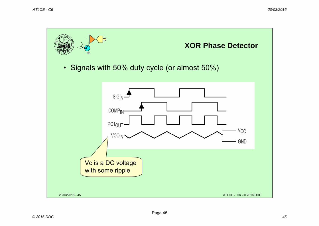
XOR Phase Detector
• Signals with 50% duty cycle (or almost 50%)
Vc is a DC voltagewith some ripple

ATLCE - C6 20/03/2016
© 2016 DDC 46Page 46
20/03/2016 - 46 ATLCE - C6 - © 2016 DDC
PFD Phase Detector
• Any duty cycle• Infinite gain (charge pump)
Vc is a constant voltage; changesonly when the phase error is ≠ 0

ATLCE - C6 20/03/2016
© 2016 DDC 47Page 47
20/03/2016 - 47 ATLCE - C6 - © 2016 DDC
SR FF Phase Detector
• Any duty cycle (PD based on transitions)
Vc is a DC voltagewith some ripple

ATLCE - C6 20/03/2016
© 2016 DDC 48Page 48
20/03/2016 - 48 ATLCE - C6 - © 2016 DDC
R1
R2
4046 VCO
• External components:– R1, R2, C
ATLCE - C6 20/03/2016
© 2016 DDC 49Page 49
20/03/2016 - 49 ATLCE - C6 - © 2016 DDC
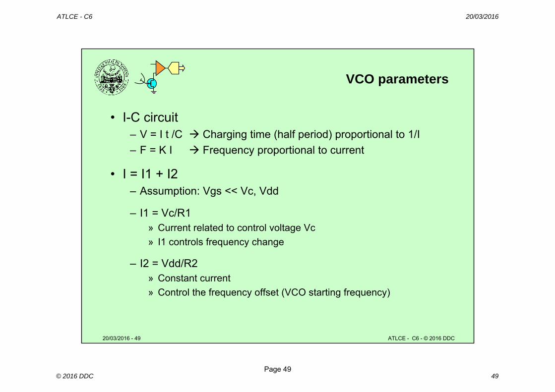
VCO parameters
• I-C circuit– V = I t /C Charging time (half period) proportional to 1/I– F = K I Frequency proportional to current
• I = I1 + I2– Assumption: Vgs << Vc, Vdd
– I1 = Vc/R1» Current related to control voltage Vc» I1 controls frequency change
– I2 = Vdd/R2» Constant current» Control the frequency offset (VCO starting frequency)

ATLCE - C6 20/03/2016
© 2016 DDC 50Page 50
20/03/2016 - 50 ATLCE - C6 - © 2016 DDC
Fo(Vc) characterisitc
• I = Vc/R1 + Vdd/R2 – Initial frequency set by R2– Slope control set by R1
Vc
f
R2R1
R1
R2I
Vdd
ATLCE - C6 20/03/2016
© 2016 DDC 51Page 51
20/03/2016 - 51 ATLCE - C6 - © 2016 DDC
Lab experiment 3
• 4046 integrated PLL:– Verification of PLL behavior and parameters– Design and test of a synthesizer
• PLL operation1) VCO Fo(Vc) characteristic2) Capture and lock ranges
• Synthesizers3) Frequency multiplication (divider using CD 4029 or FPGA)Optional:3) Synthesizer with frequency multiplication by M4) Integer synthesizer with frequency multiplication by M/N5) Fractional synthesizer

ATLCE - C6 20/03/2016
© 2016 DDC 52Page 52
20/03/2016 - 52 ATLCE - C6 - © 2016 DDC
Fully digital (or SW) solution: ADPLL
• Analog/Digital PLL: loop uses digital circuits
• Several solutions for digital processing– Wired logic– Programmable logic– Processor + SW DSPLL
• Programmable parameters, with better control
• Digital Vi ADC on Vd– Digital loop filter + Numeric Controlled Oscillator (NCO)
• Analog Vi ADC on Vi– Digital PD + Digital loop filter + NCO

ATLCE - C6 20/03/2016
© 2016 DDC 53Page 53
20/03/2016 - 53 ATLCE - C6 - © 2016 DDC
Example of DSP-PLL: Si550
• Variable frequency clock generator– Analog PD, then ADC – 10 MHz – 1,4 GHz range (Si550)
From https://www.silabs.com
VCO output (Vo)
PLL input (Vi)
control
Non volatile memory

ATLCE - C6 20/03/2016
© 2016 DDC 54Page 54
20/03/2016 - 54 ATLCE - C6 - © 2016 DDC
Lesson C6 – test questions
• Which are the circuits suitable for RF VCOs ?
• In a synthesizer the reference signal at Fr = 1 MHz is divided by 1000 towards the PD. Which is the channel step of the synthesizer ?
• Which are the benefits of “fractional” vs “integer” synthesizers ?
• Which parameter must be modified to change the output frequency of a DDS?
• How can we get phase modulation in a DDS?
• How can we get digital AM in a DDS ?
• Describe for which signal or application is best suited each of the phase demodulator (XOR, PFD, FF-SR) available in the CD 4046.