an549: the hc-5502x/4x telephone subscriber … hc-5502x/4x telephone subscriber line an549 rev 1.00...
TRANSCRIPT
The HC-5502X/4X Telephone Subscriber Line Interface Circuits (SLIC)
APPLICATION NOTE
AN549Rev 1.00
January 1997
IntroductionThe HC-5502X/4X family of telephone subscriber line interface circuits (SLIC) integrate most of the BORSCHT functions of the traditional hybrid transformer interface circuits onto one chip. The circuits are manufactured in a 200V dielectric isolation (DI) process and together with a secondary protection diode bridge give 1kV of isolation from lightning induced faults between the subscriber loop and the telephone office.
The BORSCHT functions provided are:
• Battery Feed With Loop Current Limiting
• Overvoltage Protection
• Ringing
• Supervision/Signalling
• Hybrid
The HC-5502X is intended for use in systems utilizing single ended tip (positive side) injected ringing and limits the short loop current to 30mA; the HC-5504X is intended for use in ring side (negative side) injected ringing systems and will limit the short loop current to 40mA. It should be noted that the HC-5504X can also be configured to operate in switches
employing either of the two single ended ringing methods and in balanced ringing systems.
This note will describe each subfunction of the SLIC and will discuss several system design features, including balance networks and complex impedance matching.
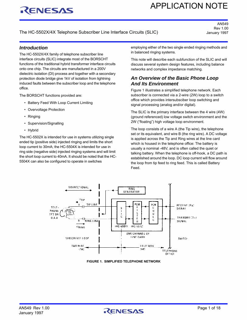
An Overview of the Basic Phone Loop And Its EnvironmentFigure 1 illustrates a simplified telephone network. Each subscriber is connected via a 2-wire (2W) loop to a switch office which provides intersubsciber loop switching and signal processing (analog and/or digital).
The SLIC is the primary interface between the 4 wire (4W) (ground referenced) low voltage switch environment and the 2W (“floating”) high voltage loop environment.
The loop consists of a wire A (the Tip wire), the telephone set or its equivalent, and wire B (the ring wire). A DC voltage is applied across the Tip and Ring wires at the line card which is housed in the telephone office: The battery is usually a nominal -48V, and is often called the quiet or talking battery. When the telephone is off-hook, a DC path is established around the loop. DC loop current will flow around the loop from tip feed to ring feed. This is called Battery Feed.
FIGURE 1. SIMPLIFIED TELEPHONE NETWORK
AN549 Rev 1.00 Page 1 of 18January 1997
The HC-5502X/4X Telephone
Subscriber Line
The SLIC must be able to sense this DC current and flag the switch controller: This is referred to as Switch Hook Detection (SHD). It tells the switch controller that the line is busy, and is a supervisory function.
The subscriber set is often located very close to the switch office. Thus, the loop resistance will be very low and the SLIC should incorporate a feedback network that will limit the loop current to a specified maximum to prevent battery power drain and minimize power dissipation at the board level. The HC-5502X/4X SLICs sense the loop current and adjust the voltage on the ring side of the line to cause line current saturation.
The telephone can be rung by switching a ring relay to connect a ring generator to the loop. The on-off switching of the relay (cadencing) is controlled by the Ring Command (RC) input which gates the relay driver output. When the user answers the telephone, the ring relay is automatically tripped, the ring command signal is inhibited and the 2W loop is made ready for voice transmission. Voice signals are transmitted onto the loop by directly modulating the DC feed. This AC voice signal is coupled to the users earpiece via a transformer in the telephone set. Voice transmission for the 2W to the 4W system is called the hybrid function. For 2W to 4W transmission, the subscriber talking into his set modulates the resistance of the telephone microphone. This causes AC current in the loop which is sensed by the SLIC and transmitted as a ground referenced voltage signal to the signal processing electronics within the switch.
Subscriber loops are usually measured in terms of loop resistance. The nominal loop length is 1200. Owing to the length of the lines and their location near power lines, common mode or longitudinal currents are often induced. The SLIC has to distinguish between these noise signals (longitudinal) and the transversal signals, and reject the unwanted longitudinal components: this is a measure of the SLIC's longitudinal balance. The primary noise sources are 60/50Hz power lines, cable cross talk, and RF transmissions. The Intersil SLICs will accommodate 15mARMS of noise currents on each side of the loop.
The line is also subjected to lightning strikes. Together with primary and secondary protection networks, the SLIC must withstand 1kV peak of lightning induced energy. In fact, the plastic encapsulated Intersil SLIC can withstand a 1kV peak strike with a small signal diode bridge providing voltage clamping and current steering.
The Intersil HC-5502X/4XThe HC-5502X/4X family of SLICs are primary intended for use within Private Branch Exchanges (PBX) although they can be used in the larger switch networks found in Central Offices (CO).
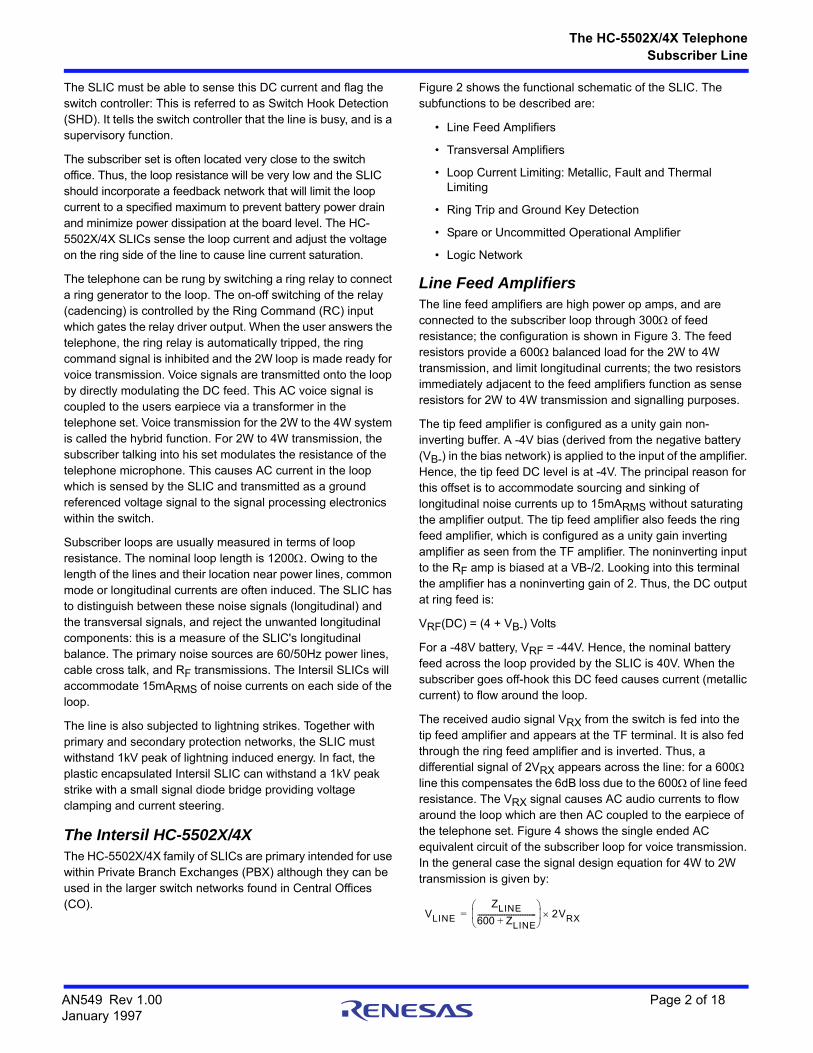
Figure 2 shows the functional schematic of the SLIC. The subfunctions to be described are:
• Line Feed Amplifiers
• Transversal Amplifiers
• Loop Current Limiting: Metallic, Fault and Thermal Limiting
• Ring Trip and Ground Key Detection
• Spare or Uncommitted Operational Amplifier
• Logic Network
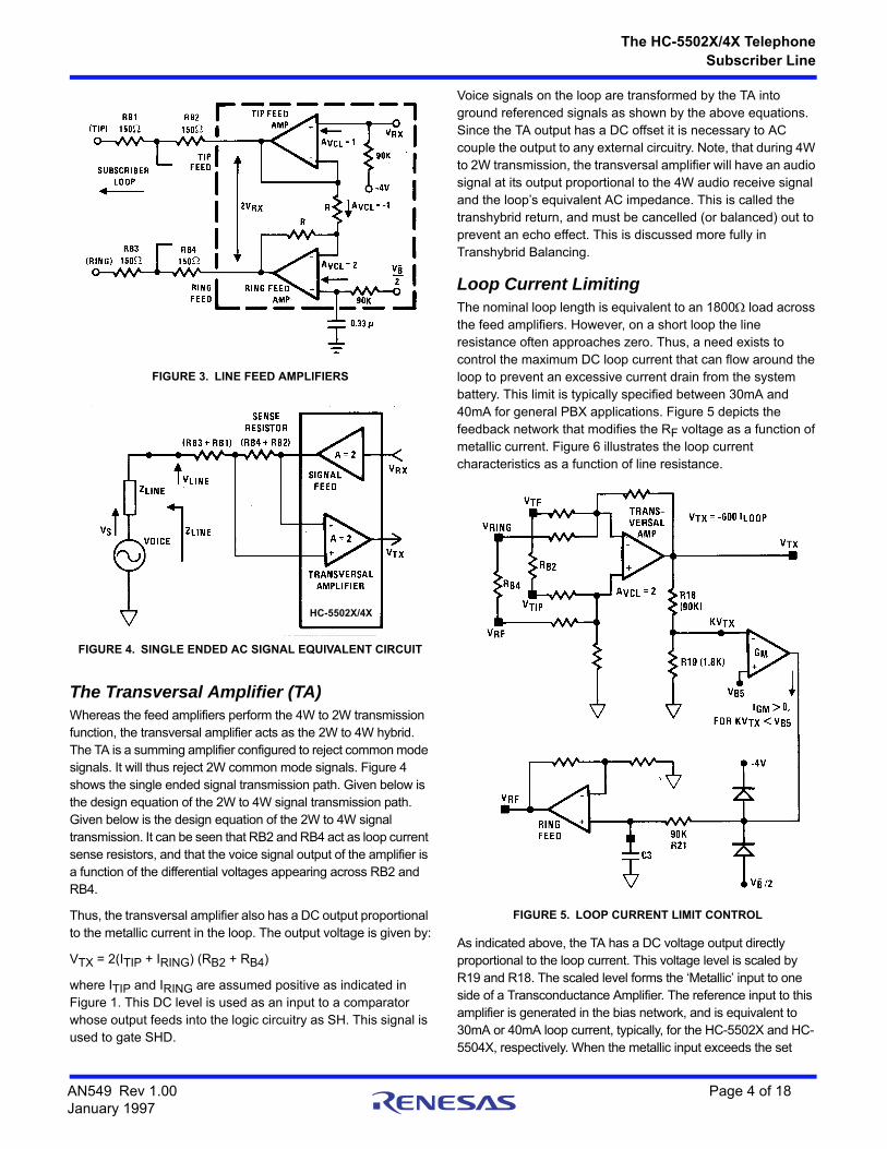
Line Feed AmplifiersThe line feed amplifiers are high power op amps, and are connected to the subscriber loop through 300 of feed resistance; the configuration is shown in Figure 3. The feed resistors provide a 600 balanced load for the 2W to 4W transmission, and limit longitudinal currents; the two resistors immediately adjacent to the feed amplifiers function as sense resistors for 2W to 4W transmission and signalling purposes.
The tip feed amplifier is configured as a unity gain non-inverting buffer. A -4V bias (derived from the negative battery (VB-) in the bias network) is applied to the input of the amplifier. Hence, the tip feed DC level is at -4V. The principal reason for this offset is to accommodate sourcing and sinking of longitudinal noise currents up to 15mARMS without saturating the amplifier output. The tip feed amplifier also feeds the ring feed amplifier, which is configured as a unity gain inverting amplifier as seen from the TF amplifier. The noninverting input to the RF amp is biased at a VB-/2. Looking into this terminal the amplifier has a noninverting gain of 2. Thus, the DC output at ring feed is:
VRF(DC) = (4 + VB-) Volts
For a -48V battery, VRF = -44V. Hence, the nominal battery feed across the loop provided by the SLIC is 40V. When the subscriber goes off-hook this DC feed causes current (metallic current) to flow around the loop.
The received audio signal VRX from the switch is fed into the tip feed amplifier and appears at the TF terminal. It is also fed through the ring feed amplifier and is inverted. Thus, a differential signal of 2VRX appears across the line: for a 600 line this compensates the 6dB loss due to the 600 of line feed resistance. The VRX signal causes AC audio currents to flow around the loop which are then AC coupled to the earpiece of the telephone set. Figure 4 shows the single ended AC equivalent circuit of the subscriber loop for voice transmission. In the general case the signal design equation for 4W to 2W transmission is given by:
VLINE
ZLINE600 ZLINE+---------------------------------
2VRX=
AN549 Rev 1.00 Page 2 of 18January 1997

The HC-5502X/4X Telephone
Subscriber Line
VB2
VB1VB2VB3VB4VB5+5V
IB1 IB2 IB3 IB4 IB5 IB6 IB7 IB8
VBAT
IB9 IB10 IB11
VB+
VB+
A-100TRANSV’LI/V AMP
-
+
IB6
R6
R5
R11
VB+
R7
R8
R10
R9
R22 R23
R3
R4
R1
R2
R16
R15
VBAT
VBAT
R12
VBAT
VB+
A-200LONG’LI/V AMP
IB7
-
+
R20
VBAT
VB+A-400
TIP FEEDAMP
IB4-
+
RINGFEED
SENSE
VBAT
VBAT
5V
VB4
IB8
RING TRIP DETECTOR
+
SWITCH HOOK
VB1IB6
+
R18
DETECTOR
VB+
QD28QD27
VBAT
- +
-
GND SHORTSCURRENTLIMITING
IB1
VB3
THERMALLIMITING
VB5
STTLAND LOGICINTERFACE
RFC
SH
GK
VB5-+
IB2
LOAD CURRENTLIMITING
R14
R13
VBAT
VBAT/2 REFERENCE
R21
VBAT
A-300RING FEED
AMP
IB5
-
+
RING
RF
TIP
TF
10
2
3
1
9
RX C4 VBATBAT ANA DIG
VB+GND GND GND
21 22 11 12 23 6 3 (4)*
+ - OUT
20 19 18
VBATIB3
VB+
VB+5V IB10
VBAT
PD
15
RC
SHD
GKD
C2
16
13
17
14
TXC3 RS RD
87245
R17
VB2
VB+
R19
VBAT
QD3 QD36
VOLTAGE AND CURRENTBIAS NETWORK
A-500OP AMP
FIGURE 2. SLIC FUNCTIONAL SCHEMATIC
C1
4*
* PIN DESIGNATION DIFFERS BETWEENHC5502X AND HC5504X
AN549 Rev 1.00 Page 3 of 18January 1997
The HC-5502X/4X Telephone
Subscriber Line
The Transversal Amplifier (TA)Whereas the feed amplifiers perform the 4W to 2W transmission function, the transversal amplifier acts as the 2W to 4W hybrid. The TA is a summing amplifier configured to reject common mode signals. It will thus reject 2W common mode signals. Figure 4 shows the single ended signal transmission path. Given below is the design equation of the 2W to 4W signal transmission path. Given below is the design equation of the 2W to 4W signal transmission. It can be seen that RB2 and RB4 act as loop current sense resistors, and that the voice signal output of the amplifier is a function of the differential voltages appearing across RB2 and RB4.
Thus, the transversal amplifier also has a DC output proportional to the metallic current in the loop. The output voltage is given by:
VTX = 2(ITIP + IRING) (RB2 + RB4)
where ITIP and IRING are assumed positive as indicated in Figure 1. This DC level is used as an input to a comparator whose output feeds into the logic circuitry as SH. This signal is used to gate SHD.
Voice signals on the loop are transformed by the TA into ground referenced signals as shown by the above equations. Since the TA output has a DC offset it is necessary to AC couple the output to any external circuitry. Note, that during 4W to 2W transmission, the transversal amplifier will have an audio signal at its output proportional to the 4W audio receive signal and the loop’s equivalent AC impedance. This is called the transhybrid return, and must be cancelled (or balanced) out to prevent an echo effect. This is discussed more fully in Transhybrid Balancing.
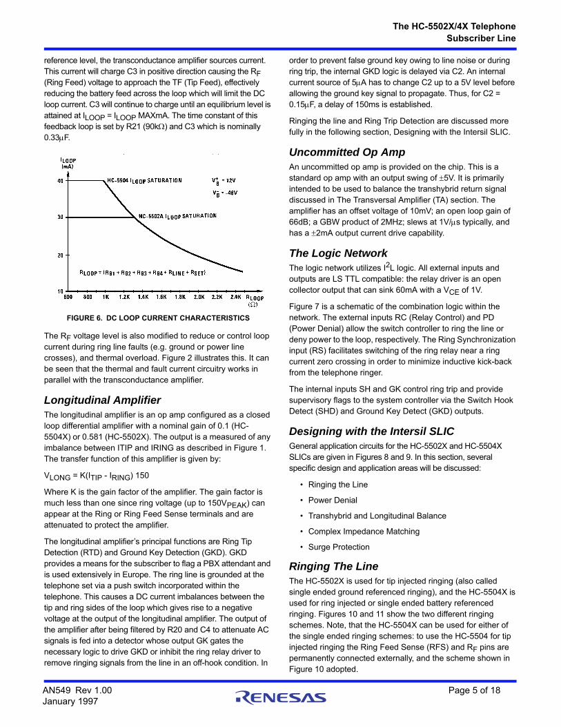
Loop Current LimitingThe nominal loop length is equivalent to an 1800 load across the feed amplifiers. However, on a short loop the line resistance often approaches zero. Thus, a need exists to control the maximum DC loop current that can flow around the loop to prevent an excessive current drain from the system battery. This limit is typically specified between 30mA and 40mA for general PBX applications. Figure 5 depicts the feedback network that modifies the RF voltage as a function of metallic current. Figure 6 illustrates the loop current characteristics as a function of line resistance.
As indicated above, the TA has a DC voltage output directly proportional to the loop current. This voltage level is scaled by R19 and R18. The scaled level forms the ‘Metallic’ input to one side of a Transconductance Amplifier. The reference input to this amplifier is generated in the bias network, and is equivalent to 30mA or 40mA loop current, typically, for the HC-5502X and HC-5504X, respectively. When the metallic input exceeds the set
FIGURE 3. LINE FEED AMPLIFIERS
FIGURE 4. SINGLE ENDED AC SIGNAL EQUIVALENT CIRCUIT
HC-5502X/4X
FIGURE 5. LOOP CURRENT LIMIT CONTROL
AN549 Rev 1.00 Page 4 of 18January 1997
The HC-5502X/4X Telephone
Subscriber Line
reference level, the transconductance amplifier sources current. This current will charge C3 in positive direction causing the RF (Ring Feed) voltage to approach the TF (Tip Feed), effectively reducing the battery feed across the loop which will limit the DC loop current. C3 will continue to charge until an equilibrium level is attained at ILOOP = ILOOP MAXmA. The time constant of this feedback loop is set by R21 (90k) and C3 which is nominally 0.33F.
The RF voltage level is also modified to reduce or control loop current during ring line faults (e.g. ground or power line crosses), and thermal overload. Figure 2 illustrates this. It can be seen that the thermal and fault current circuitry works in parallel with the transconductance amplifier.
Longitudinal AmplifierThe longitudinal amplifier is an op amp configured as a closed loop differential amplifier with a nominal gain of 0.1 (HC-5504X) or 0.581 (HC-5502X). The output is a measured of any imbalance between ITIP and IRING as described in Figure 1. The transfer function of this amplifier is given by:
VLONG = K(ITIP - IRING) 150
Where K is the gain factor of the amplifier. The gain factor is much less than one since ring voltage (up to 150VPEAK) can appear at the Ring or Ring Feed Sense terminals and are attenuated to protect the amplifier.
The longitudinal amplifier’s principal functions are Ring Tip Detection (RTD) and Ground Key Detection (GKD). GKD provides a means for the subscriber to flag a PBX attendant and is used extensively in Europe. The ring line is grounded at the telephone set via a push switch incorporated within the telephone. This causes a DC current imbalances between the tip and ring sides of the loop which gives rise to a negative voltage at the output of the longitudinal amplifier. The output of the amplifier after being filtered by R20 and C4 to attenuate AC signals is fed into a detector whose output GK gates the necessary logic to drive GKD or inhibit the ring relay driver to remove ringing signals from the line in an off-hook condition. In
order to prevent false ground key owing to line noise or during ring trip, the internal GKD logic is delayed via C2. An internal current source of 5A has to change C2 up to a 5V level before allowing the ground key signal to propagate. Thus, for C2 = 0.15F, a delay of 150ms is established.
Ringing the line and Ring Trip Detection are discussed more fully in the following section, Designing with the Intersil SLIC.
Uncommitted Op AmpAn uncommitted op amp is provided on the chip. This is a standard op amp with an output swing of 5V. It is primarily intended to be used to balance the transhybrid return signal discussed in The Transversal Amplifier (TA) section. The amplifier has an offset voltage of 10mV; an open loop gain of 66dB; a GBW product of 2MHz; slews at 1V/s typically, and has a 2mA output current drive capability.
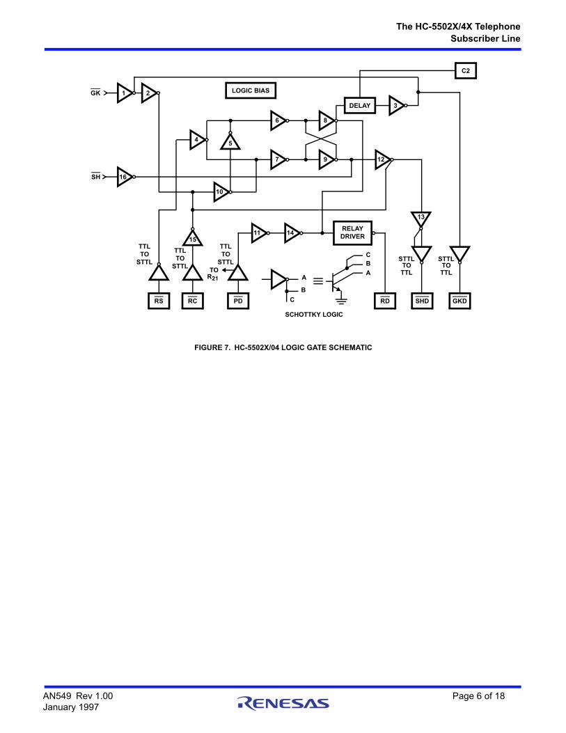
The Logic NetworkThe logic network utilizes I2L logic. All external inputs and outputs are LS TTL compatible: the relay driver is an open collector output that can sink 60mA with a VCE of 1V.
Figure 7 is a schematic of the combination logic within the network. The external inputs RC (Relay Control) and PD (Power Denial) allow the switch controller to ring the line or deny power to the loop, respectively. The Ring Synchronization input (RS) facilitates switching of the ring relay near a ring current zero crossing in order to minimize inductive kick-back from the telephone ringer.
The internal inputs SH and GK control ring trip and provide supervisory flags to the system controller via the Switch Hook Detect (SHD) and Ground Key Detect (GKD) outputs.
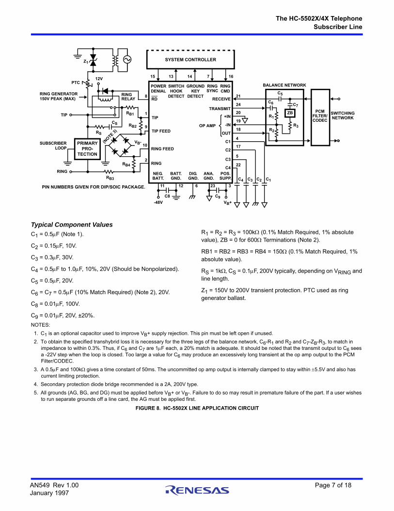
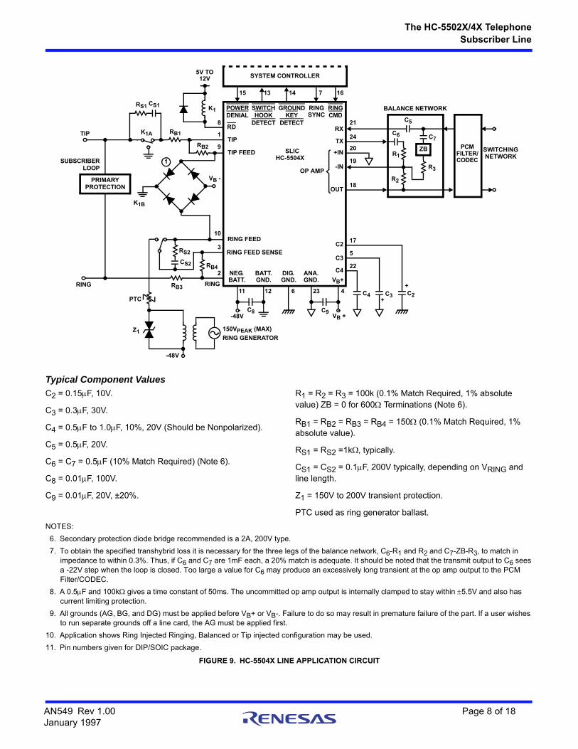
Designing with the Intersil SLICGeneral application circuits for the HC-5502X and HC-5504X SLICs are given in Figures 8 and 9. In this section, several specific design and application areas will be discussed:
• Ringing the Line
• Power Denial
• Transhybrid and Longitudinal Balance
• Complex Impedance Matching
• Surge Protection
Ringing The LineThe HC-5502X is used for tip injected ringing (also called single ended ground referenced ringing), and the HC-5504X is used for ring injected or single ended battery referenced ringing. Figures 10 and 11 show the two different ringing schemes. Note, that the HC-5504X can be used for either of the single ended ringing schemes: to use the HC-5504 for tip injected ringing the Ring Feed Sense (RFS) and RF pins are permanently connected externally, and the scheme shown in Figure 10 adopted.
FIGURE 6. DC LOOP CURRENT CHARACTERISTICS
AN549 Rev 1.00 Page 5 of 18January 1997
The HC-5502X/4X Telephone
Subscriber Line
FIGURE 7. HC-5502X/04 LOGIC GATE SCHEMATIC
15
5
6
12
4
16
13
A
B
C
CB
A
TTLTO
STTL
TTLTO
STTL
TTLTO
STTLTO
R21
GKDSHDRDPDRCRS
C2
TTLTO
STTL
TTLTO
STTL
DELAY
LOGIC BIAS
RELAYDRIVER
SH
GK
11 14
3
97
8
10
21
SCHOTTKY LOGIC
AN549 Rev 1.00 Page 6 of 18January 1997
The HC-5502X/4X Telephone
Subscriber Line
Typical Component Values
C1 = 0.5F (Note 1).
C2 = 0.15F, 10V.
C3 = 0.3F, 30V.
C4 = 0.5F to 1.0F, 10%, 20V (Should be Nonpolarized).
C5 = 0.5F, 20V.
C6 = C7 = 0.5F (10% Match Required) (Note 2), 20V.
C8 = 0.01F, 100V.
C9 = 0.01F, 20V, ±20%.
R1 = R2 = R3 = 100k (0.1% Match Required, 1% absolute value), ZB = 0 for 600 Terminations (Note 2).
RB1 = RB2 = RB3 = RB4 = 150 (0.1% Match Required, 1% absolute value).
RS = 1k, CS = 0.1F, 200V typically, depending on VRING and line length.
Z1 = 150V to 200V transient protection. PTC used as ring generator ballast.
NOTES:
1. C1 is an optional capacitor used to improve VB+ supply rejection. This pin must be left open if unused.
2. To obtain the specified transhybrid loss it is necessary for the three legs of the balance network, C6-R1 and R2 and C7-ZB-R3, to match in impedance to within 0.3%. Thus, if C6 and C7 are 1F each, a 20% match is adequate. It should be noted that the transmit output to C6 sees a -22V step when the loop is closed. Too large a value for C6 may produce an excessively long transient at the op amp output to the PCM Filter/CODEC.
3. A 0.5F and 100k gives a time constant of 50ms. The uncommitted op amp output is internally clamped to stay within 5.5V and also has current limiting protection.
4. Secondary protection diode bridge recommended is a 2A, 200V type.
5. All grounds (AG, BG, and DG) must be applied before VB+ or VB-. Failure to do so may result in premature failure of the part. If a user wishes to run separate grounds off a line card, the AG must be applied first.
FIGURE 8. HC-5502X LINE APPLICATION CIRCUIT
PRIMARYPRO-
TECTIONRING FEED
RING
8
1
9
10
2
TIP FEED
TIP
RD
OP AMP
RECEIVE
TRANSMIT
+IN
-IN
OUT
C2
C3
C4NEG.BATT.
BATT.GND.
DIG.GND.
ANA.GND.
POWERDENIAL
SWITCHHOOK
DETECT
GROUNDKEY
DETECT
RINGSYNC
RINGCMD
C1
C6
R1
R2
C7
C5
R3
BALANCE NETWORK
PCMFILTER/CODEC
SWITCHINGNETWORK
ZB
C4 C3 C2 C1
23
C9
3
VB+
POS.SUPP.
61211
C8
-48V
Z1
PTC12V
RINGRELAY
RB1
RB2
VB-
RB4
RING
RB3
RS
CS
TIP
SUBSCRIBERLOOP
150V PEAK (MAX)RING GENERATOR
SYSTEM CONTROLLER
15 13 14 7 16
21
24
20
19
18
4
17
5
22
(NOTE 3
)
PIN NUMBERS GIVEN FOR DIP/SOIC PACKAGE.
AN549 Rev 1.00 Page 7 of 18January 1997
The HC-5502X/4X Telephone
Subscriber Line
Typical Component Values
C2 = 0.15F, 10V.
C3 = 0.3F, 30V.
C4 = 0.5F to 1.0F, 10%, 20V (Should be Nonpolarized).
C5 = 0.5F, 20V.
C6 = C7 = 0.5F (10% Match Required) (Note 6).
C8 = 0.01F, 100V.
C9 = 0.01F, 20V, ±20%.
R1 = R2 = R3 = 100k (0.1% Match Required, 1% absolute value) ZB = 0 for 600 Terminations (Note 6).
RB1 = RB2 = RB3 = RB4 = 150 (0.1% Match Required, 1% absolute value).
RS1 = RS2 =1k, typically.
CS1 = CS2 = 0.1F, 200V typically, depending on VRING and line length.
Z1 = 150V to 200V transient protection.
PTC used as ring generator ballast.
NOTES:
6. Secondary protection diode bridge recommended is a 2A, 200V type.
7. To obtain the specified transhybrid loss it is necessary for the three legs of the balance network, C6-R1 and R2 and C7-ZB-R3, to match in impedance to within 0.3%. Thus, if C6 and C7 are 1mF each, a 20% match is adequate. It should be noted that the transmit output to C6 sees a -22V step when the loop is closed. Too large a value for C6 may produce an excessively long transient at the op amp output to the PCM Filter/CODEC.
8. A 0.5F and 100k gives a time constant of 50ms. The uncommitted op amp output is internally clamped to stay within 5.5V and also has current limiting protection.
9. All grounds (AG, BG, and DG) must be applied before VB+ or VB-. Failure to do so may result in premature failure of the part. If a user wishes to run separate grounds off a line card, the AG must be applied first.
10. Application shows Ring Injected Ringing, Balanced or Tip injected configuration may be used.
11. Pin numbers given for DIP/SOIC package.
FIGURE 9. HC-5504X LINE APPLICATION CIRCUIT
RB4
K1B
K1A
RING
RING FEED
RING FEED SENSE
TIP
VB -
SLICHC-5504X
RS1
RB2
RB1
PTC
Z1
-48V
150VPEAK (MAX)
RING GENERATOR
RINGRB3
RS2
CS2
SUBSCRIBERLOOP
-48V
SYSTEM CONTROLLER
K1
8
1
9
10
3
2
1
TIP FEED
TIP
RD
OP AMP
RX
TX
+IN
-IN
OUT
C2
C3
C4NEG.BATT.
BATT.GND.
DIG.GND.
ANA.GND. VB+
POWERDENIAL
SWITCHHOOK
DETECT
GROUNDKEY
DETECT
RINGSYNC
RINGCMD
15 13 14 7 16
11 12 6 23
C9
4
VB +C8
C4 C3 C2
+
+
21
24
20
19
18
17
5
22
C6
R1
R2
C7
C5
R3
BALANCE NETWORK
PCMFILTER/CODEC
SWITCHINGNETWORK
ZB
5V TO12V
PRIMARYPROTECTION
CS1
AN549 Rev 1.00 Page 8 of 18January 1997

The HC-5502X/4X Telephone
Subscriber Line
FIGURE 10. HC-5502X TIP INJECTED SINGLE ENDED RINGING
FIGURE 11. HC-5504X RING INJECTED SINGLE ENDED RINGING
HC-5502X
HC-5504X
AN549 Rev 1.00 Page 9 of 18January 1997
The HC-5502X/4X Telephone
Subscriber Line
The Ring Command (RC) input is taken low during ringing. This activates the ring relay driver (RR) output providing the telephone is not off-hook or the line is not in a power denial state. The ring relay connects the ring generator to the subscriber loop. The ring generator output is usually an 80VRMS, 20Hz signal. For use with the Intersil SLIC, the ring signal should not exceed 150V peak. Since the telephone ringer is AC coupled only ring current will flow. For the HC-5502X SLIC, the ring current is sunk by the ring feed amplifier output stage whereas for the HC-5504X the ring path flows directly into VB- via a set of relay contacts. The high impedance terminal RFS exists on the HC-5504X so that the low impedance RF node can be isolated from the hot end of the ring path in the battery referenced ring scheme.
The AC ring current flowing in the subscriber circuit will be sensed across RB4, and will give rise to an AC voltage at the output of the longitudinal amplifier. R20 and C4 attenuate this signal before it reaches the ring trip detector to prevent false ring trip. C4 is nominally set at 0.47F but can be increased towards 1F for short lines or if several telephones are connected in parallel across the line in order to prevent false or intermittent ring trip.
When the subscriber goes off-hook, a DC path is established between the output winding of the ring generator and the battery ground or VB- terminal. A DC longitudinal imbalance is established since no tip feed current is flowing through the tip feed resistors. The longitudinal amplifier output is driven negative. Once it exceeds the ring trip threshold of the ring trip detector, the logic circuitry is driven by GK to trip the ring relay
establishing an off-hook condition such that SHD will become active as loop metallic current starts to flow.
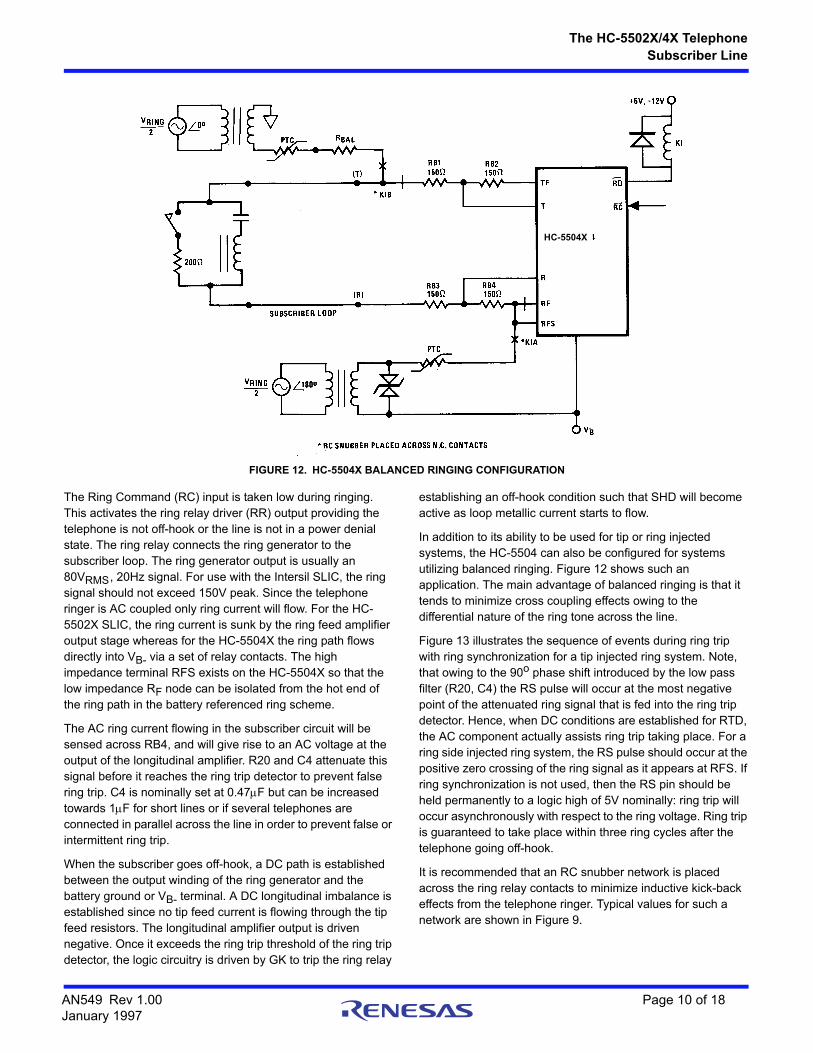
In addition to its ability to be used for tip or ring injected systems, the HC-5504 can also be configured for systems utilizing balanced ringing. Figure 12 shows such an application. The main advantage of balanced ringing is that it tends to minimize cross coupling effects owing to the differential nature of the ring tone across the line.
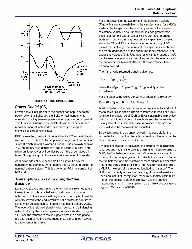
Figure 13 illustrates the sequence of events during ring trip with ring synchronization for a tip injected ring system. Note, that owing to the 90o phase shift introduced by the low pass filter (R20, C4) the RS pulse will occur at the most negative point of the attenuated ring signal that is fed into the ring trip detector. Hence, when DC conditions are established for RTD, the AC component actually assists ring trip taking place. For a ring side injected ring system, the RS pulse should occur at the positive zero crossing of the ring signal as it appears at RFS. If ring synchronization is not used, then the RS pin should be held permanently to a logic high of 5V nominally: ring trip will occur asynchronously with respect to the ring voltage. Ring trip is guaranteed to take place within three ring cycles after the telephone going off-hook.
It is recommended that an RC snubber network is placed across the ring relay contacts to minimize inductive kick-back effects from the telephone ringer. Typical values for such a network are shown in Figure 9.
FIGURE 12. HC-5504X BALANCED RINGING CONFIGURATION
HC-5504X
AN549 Rev 1.00 Page 10 of 18January 1997
The HC-5502X/4X Telephone
Subscriber Line
Power Denial (PD)Power denial limits power to the subscriber loop: it does not power down the SLIC, i.e., the SLIC will still consume its normal on-hook quiescent power during a power denial period. This function is intended to “isolate” from the battery, under processor control, selected subscriber loops during an overload or similar fault status.
If PD is selected, the logic circuitry inhabits RC and switches in a current source to C3. The capacitor charges up to a nominal -3.5V at which point it is clamped. Since TF is always biases at -4V, the battery feed across the loop is essentially zero, and minimum loop power will be dissipated if the circuit goes off-hook. No signalling functions are available during this mode.
After power denial is released (PD = 1), it will be several hundred milliseconds (300ms) before the RF output reaches its nominal battery setting. This is due to the RC time constant of R21 and C3.
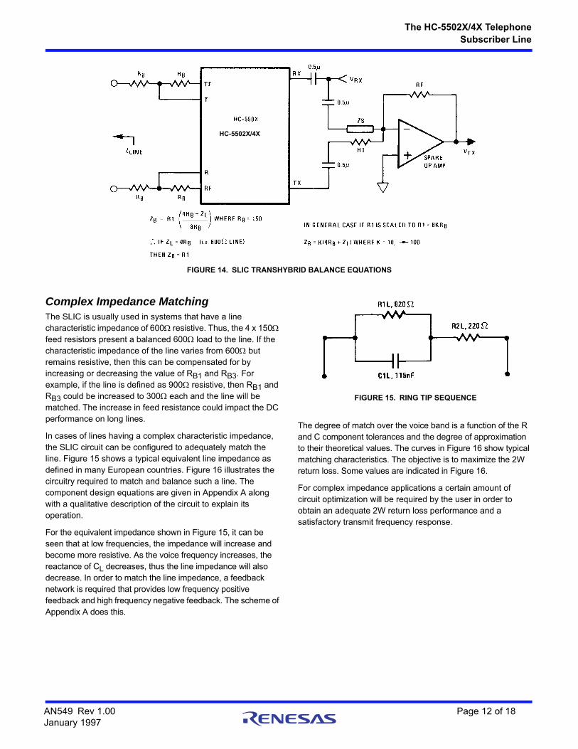
Transhybrid Loss and Longitudinal BalanceDuring 4W to 2W transmission, the 4W signal is returned to the transmit output: this is called transhybrid return: it is not a reflection from the line as it will only occur if the loop is closed. In order to prevent echo and instability in the switch, this returned signal must be balanced out before it reaches the filter/CODEC. The level of the returned signal is given below, and a balancing network utilizing the on-chip spare op amp is indicated in Figure 14. Since the returned received signal’s amplitude and phase are a function of the line’s AC impedance, the balance network is a function of the same.
For a resistive line, the two arms of the balance network (Figure 14) are also resistive. In the simplest case, for a 600 system, the two parts of the summing network have equi-resistance values. For a transhybrid balance greater than 36dB, component tolerances of 0.5% are recommended. Both arms of the summing network are capacitively coupled since the TA and TF amplifiers have output and input DC biases, respectively. The values of the capacitors are chosen to prevent degradation of the audio frequency response. For capacitive values of 0.5F, components with tolerances of 10% can be used since at voice band frequencies the reactance of the capacitor has minimal effect on the impedance of the balance network.
The transhybrid returned signal is given by:
where R = (RB1 + RB2) = (RB3 + RB4), and ZL = Line Impedance.
For the balance network, the general equation is given by:
ZB = 2R + ZL with R1 = 4R in Figure 14.
A full derivation of the balance equation is given in Appendix 1. A measure off this balance is known as transhybrid loss. For a 600 resistive line, a balance of 40dB at 1kHz is attainable. In practice owing to variations in lines and telephone sets the balance is usually lower than in the ideal case: A balance in the order of 25dB will often be measured and accepted.
By switching out the balance network, it is possible for the controller to conduct loop back tests providing the loop can be closed via a test relay in the line card.
Longitudinal balance is equivalent to common mode rejection ratio. Looking into the line card tip and ring terminals towards the SLIC, the 2W balance is a function of the impedance match between tip and ring to ground. The 4W balance is a function of the 2W balance, and the matching of the feedback resistor ratios around the transversal amplifier. (The TA itself must also exhibit a CMRR in excess of the required longitudinal balance.) The SLIC user can only control the matching of the feed resistors. For a nominal 60dB of rejection, these must match within 0.1%. The on-chip resistors are thin film SiCr resistors and are matched within 0.1%. The amplifier has a CMRR of 70dB giving a typical 4W balance of 60dB.
FIGURE 13. RING TIP SEQUENCE
VTX VRX–=4R
2R ZL+ --------------------------
AN549 Rev 1.00 Page 11 of 18January 1997
The HC-5502X/4X Telephone
Subscriber Line
Complex Impedance MatchingThe SLIC is usually used in systems that have a line characteristic impedance of 600 resistive. Thus, the 4 x 150 feed resistors present a balanced 600 load to the line. If the characteristic impedance of the line varies from 600 but remains resistive, then this can be compensated for by increasing or decreasing the value of RB1 and RB3. For example, if the line is defined as 900 resistive, then RB1 and RB3 could be increased to 300 each and the line will be matched. The increase in feed resistance could impact the DC performance on long lines.
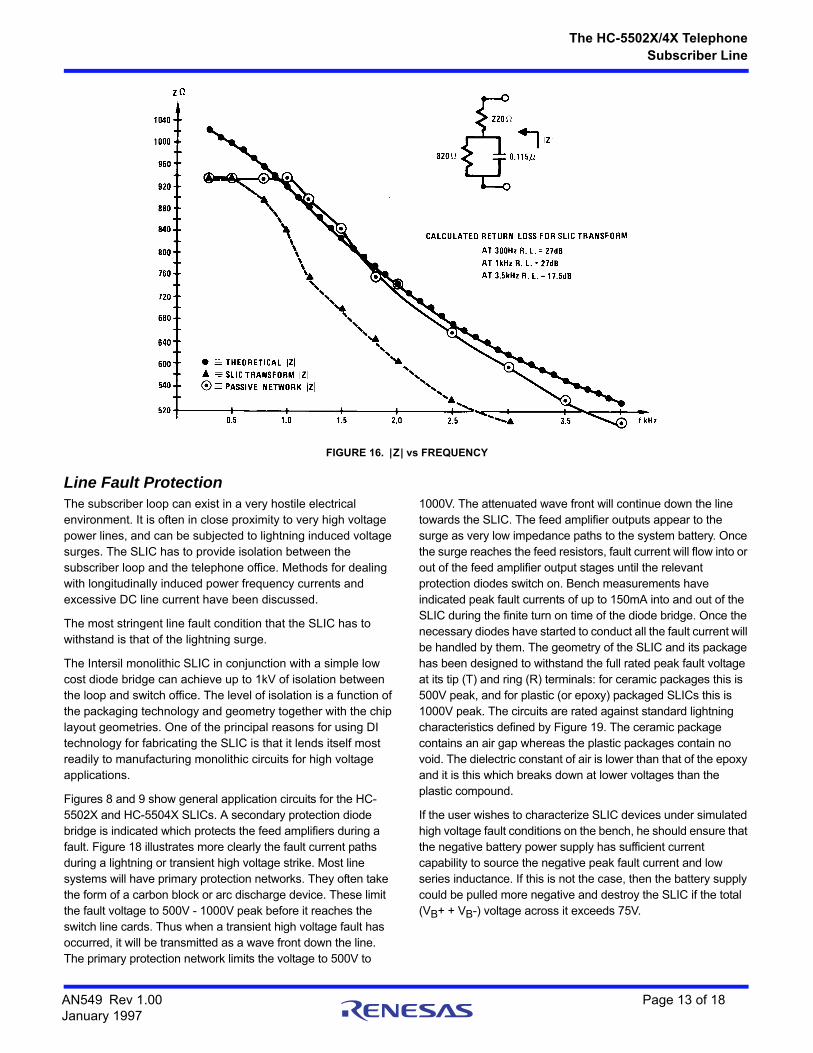
In cases of lines having a complex characteristic impedance, the SLIC circuit can be configured to adequately match the line. Figure 15 shows a typical equivalent line impedance as defined in many European countries. Figure 16 illustrates the circuitry required to match and balance such a line. The component design equations are given in Appendix A along with a qualitative description of the circuit to explain its operation.
For the equivalent impedance shown in Figure 15, it can be seen that at low frequencies, the impedance will increase and become more resistive. As the voice frequency increases, the reactance of CL decreases, thus the line impedance will also decrease. In order to match the line impedance, a feedback network is required that provides low frequency positive feedback and high frequency negative feedback. The scheme of Appendix A does this.
The degree of match over the voice band is a function of the R and C component tolerances and the degree of approximation to their theoretical values. The curves in Figure 16 show typical matching characteristics. The objective is to maximize the 2W return loss. Some values are indicated in Figure 16.
For complex impedance applications a certain amount of circuit optimization will be required by the user in order to obtain an adequate 2W return loss performance and a satisfactory transmit frequency response.
FIGURE 14. SLIC TRANSHYBRID BALANCE EQUATIONS
HC-5502X/4X
FIGURE 15. RING TIP SEQUENCE
AN549 Rev 1.00 Page 12 of 18January 1997
The HC-5502X/4X Telephone
Subscriber Line
Line Fault ProtectionThe subscriber loop can exist in a very hostile electrical environment. It is often in close proximity to very high voltage power lines, and can be subjected to lightning induced voltage surges. The SLIC has to provide isolation between the subscriber loop and the telephone office. Methods for dealing with longitudinally induced power frequency currents and excessive DC line current have been discussed.
The most stringent line fault condition that the SLIC has to withstand is that of the lightning surge.
The Intersil monolithic SLIC in conjunction with a simple low cost diode bridge can achieve up to 1kV of isolation between the loop and switch office. The level of isolation is a function of the packaging technology and geometry together with the chip layout geometries. One of the principal reasons for using DI technology for fabricating the SLIC is that it lends itself most readily to manufacturing monolithic circuits for high voltage applications.
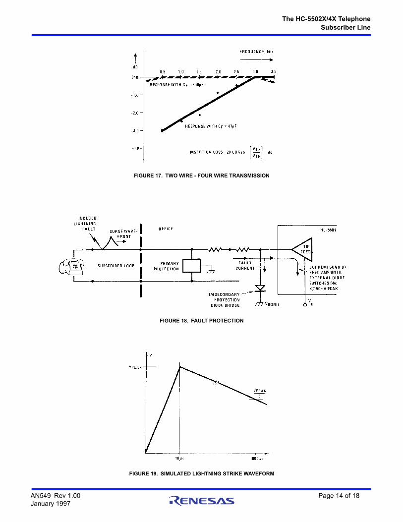
Figures 8 and 9 show general application circuits for the HC-5502X and HC-5504X SLICs. A secondary protection diode bridge is indicated which protects the feed amplifiers during a fault. Figure 18 illustrates more clearly the fault current paths during a lightning or transient high voltage strike. Most line systems will have primary protection networks. They often take the form of a carbon block or arc discharge device. These limit the fault voltage to 500V - 1000V peak before it reaches the switch line cards. Thus when a transient high voltage fault has occurred, it will be transmitted as a wave front down the line. The primary protection network limits the voltage to 500V to
1000V. The attenuated wave front will continue down the line towards the SLIC. The feed amplifier outputs appear to the surge as very low impedance paths to the system battery. Once the surge reaches the feed resistors, fault current will flow into or out of the feed amplifier output stages until the relevant protection diodes switch on. Bench measurements have indicated peak fault currents of up to 150mA into and out of the SLIC during the finite turn on time of the diode bridge. Once the necessary diodes have started to conduct all the fault current will be handled by them. The geometry of the SLIC and its package has been designed to withstand the full rated peak fault voltage at its tip (T) and ring (R) terminals: for ceramic packages this is 500V peak, and for plastic (or epoxy) packaged SLICs this is 1000V peak. The circuits are rated against standard lightning characteristics defined by Figure 19. The ceramic package contains an air gap whereas the plastic packages contain no void. The dielectric constant of air is lower than that of the epoxy and it is this which breaks down at lower voltages than the plastic compound.
If the user wishes to characterize SLIC devices under simulated high voltage fault conditions on the bench, he should ensure that the negative battery power supply has sufficient current capability to source the negative peak fault current and low series inductance. If this is not the case, then the battery supply could be pulled more negative and destroy the SLIC if the total (VB+ + VB-) voltage across it exceeds 75V.
FIGURE 16. |Z| vs FREQUENCY
AN549 Rev 1.00 Page 13 of 18January 1997
The HC-5502X/4X Telephone
Subscriber Line
FIGURE 17. TWO WIRE - FOUR WIRE TRANSMISSION
FIGURE 18. FAULT PROTECTION
FIGURE 19. SIMULATED LIGHTNING STRIKE WAVEFORM
AN549 Rev 1.00 Page 14 of 18January 1997

The HC-5502X/4X Telephone
Subscriber Line
Appendix A
Complex Line Impedance Matching with SLIC
Consider Figure A1. Assume VRX = 0.(2W to 4W transmission). At match:
This matching equation can be realized as shown in Figure A2.
FIGURE A1. TWO TO FOUR WIRE TRANSMISSION. SINGLE ENDED AC EQUIVALENT CIRCUIT OF SUBSCRIBER LOOP.
isVT
2Zo-----------
VmZo---------= =
Zo 2RF Zo'+=
Zo'Vois-------=
Vo Zo' is isZo 2isRF–==
but Vm = isZo Vo Vm 2isRF–=; (EQ. 1)
(EQ. 2)
Vs isRF VsRF
2RF Zo'+ ------------------------------- Vm=,=
Vm isRF 2RF Zo'+
RF-------------------------------=
2 in 1 for Vm, and Zo = 2RF Zo'+
Vo 2VsZo
2RF----------- 1– =
FIGURE A2. FOUR WIRE TO TWO WIRE TRANSMISSION
AN549 Rev 1.00 Page 15 of 18January 1997
The HC-5502X/4X Telephone
Subscriber Line
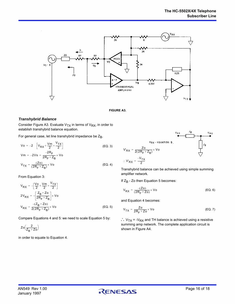
Transhybrid Balance
Consider Figure A3. Evaluate VTX in terms of VRX, in order to establish transhybrid balance equation.
For general case, let line transhybrid impedance be ZB.
From Equation 3:
Compare Equations 4 and 5: we need to scale Equation 5 by:
in order to equate to Equation 4.
Transhybrid balance can be achieved using simple summing amplifier network.
If ZB - Zo then Equation 5 becomes:
and Equation 4 becomes:
VTX = -VRX and TH balance is achieved using a resistive summing amp network. The complete application circuit is shown in Figure A4.
FIGURE A3.
Vo 2 VRXVm2---------
VTX2
-----------+ +–=
Vm 2Vs–2RF–
2RF ZB+------------------------- Vo= =
VTXZo
2RF ZB+ ------------------------------ Vo=
(EQ. 3)
(EQ. 4)
VRXVo2-------
Vm2---------
VTX2
-----------+ +–=
2VRX
ZB Zo+
2RF ZB+------------------------- Vo–=
VRX
ZB Zo+ –
2 2RF ZB+ ---------------------------------- Vo= (EQ. 5)
Zo2
ZB Zo+---------------------
V'RXZo
2 2RF ZB+ ---------------------------------- Vo=
V'RXVTX–
2--------------=
5
VRXZo –
2RF Zo+ ------------------------------ Vo= (EQ. 6)
VTXZo
2RF Zo+------------------------- Vo= (EQ. 7)
AN549 Rev 1.00 Page 16 of 18January 1997
The HC-5502X/4X Telephone
Subscriber Line
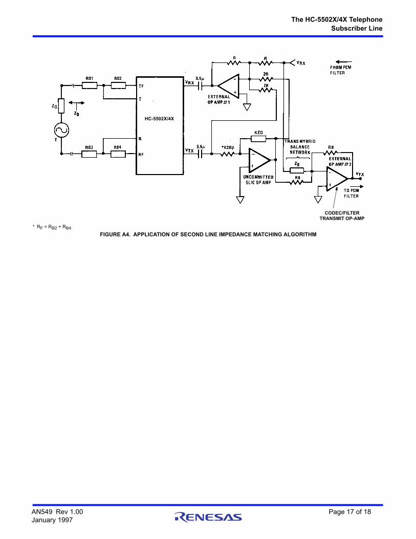
* RF = RB2 + RB4.
FIGURE A4. APPLICATION OF SECOND LINE IMPEDANCE MATCHING ALGORITHM
HC-5502X/4X
CODEC/FILTERTRANSMIT OP-AMP
AN549 Rev 1.00 Page 17 of 18January 1997

http://www.renesas.comRefer to "http://www.renesas.com/" for the latest and detailed information.
Renesas Electronics America Inc.1001 Murphy Ranch Road, Milpitas, CA 95035, U.S.A.Tel: +1-408-432-8888, Fax: +1-408-434-5351Renesas Electronics Canada Limited9251 Yonge Street, Suite 8309 Richmond Hill, Ontario Canada L4C 9T3Tel: +1-905-237-2004Renesas Electronics Europe LimitedDukes Meadow, Millboard Road, Bourne End, Buckinghamshire, SL8 5FH, U.KTel: +44-1628-651-700, Fax: +44-1628-651-804Renesas Electronics Europe GmbHArcadiastrasse 10, 40472 Düsseldorf, Germany Tel: +49-211-6503-0, Fax: +49-211-6503-1327Renesas Electronics (China) Co., Ltd.Room 1709 Quantum Plaza, No.27 ZhichunLu, Haidian District, Beijing, 100191 P. R. ChinaTel: +86-10-8235-1155, Fax: +86-10-8235-7679Renesas Electronics (Shanghai) Co., Ltd.Unit 301, Tower A, Central Towers, 555 Langao Road, Putuo District, Shanghai, 200333 P. R. China Tel: +86-21-2226-0888, Fax: +86-21-2226-0999Renesas Electronics Hong Kong LimitedUnit 1601-1611, 16/F., Tower 2, Grand Century Place, 193 Prince Edward Road West, Mongkok, Kowloon, Hong KongTel: +852-2265-6688, Fax: +852 2886-9022Renesas Electronics Taiwan Co., Ltd.13F, No. 363, Fu Shing North Road, Taipei 10543, TaiwanTel: +886-2-8175-9600, Fax: +886 2-8175-9670Renesas Electronics Singapore Pte. Ltd.80 Bendemeer Road, Unit #06-02 Hyflux Innovation Centre, Singapore 339949Tel: +65-6213-0200, Fax: +65-6213-0300Renesas Electronics Malaysia Sdn.Bhd.Unit 1207, Block B, Menara Amcorp, Amcorp Trade Centre, No. 18, Jln Persiaran Barat, 46050 Petaling Jaya, Selangor Darul Ehsan, MalaysiaTel: +60-3-7955-9390, Fax: +60-3-7955-9510Renesas Electronics India Pvt. Ltd.No.777C, 100 Feet Road, HAL 2nd Stage, Indiranagar, Bangalore 560 038, IndiaTel: +91-80-67208700, Fax: +91-80-67208777Renesas Electronics Korea Co., Ltd.17F, KAMCO Yangjae Tower, 262, Gangnam-daero, Gangnam-gu, Seoul, 06265 KoreaTel: +82-2-558-3737, Fax: +82-2-558-5338
SALES OFFICES
© 2018 Renesas Electronics Corporation. All rights reserved.Colophon 7.0
(Rev.4.0-1 November 2017)
Notice
1. Descriptions of circuits, software and other related information in this document are provided only to illustrate the operation of semiconductor products and application examples. You are fully responsible for
the incorporation or any other use of the circuits, software, and information in the design of your product or system. Renesas Electronics disclaims any and all liability for any losses and damages incurred by
you or third parties arising from the use of these circuits, software, or information.
2. Renesas Electronics hereby expressly disclaims any warranties against and liability for infringement or any other claims involving patents, copyrights, or other intellectual property rights of third parties, by or
arising from the use of Renesas Electronics products or technical information described in this document, including but not limited to, the product data, drawings, charts, programs, algorithms, and application
examples.
3. No license, express, implied or otherwise, is granted hereby under any patents, copyrights or other intellectual property rights of Renesas Electronics or others.
4. You shall not alter, modify, copy, or reverse engineer any Renesas Electronics product, whether in whole or in part. Renesas Electronics disclaims any and all liability for any losses or damages incurred by
you or third parties arising from such alteration, modification, copying or reverse engineering.
5. Renesas Electronics products are classified according to the following two quality grades: “Standard” and “High Quality”. The intended applications for each Renesas Electronics product depends on the
product’s quality grade, as indicated below.
"Standard": Computers; office equipment; communications equipment; test and measurement equipment; audio and visual equipment; home electronic appliances; machine tools; personal electronic
equipment; industrial robots; etc.
"High Quality": Transportation equipment (automobiles, trains, ships, etc.); traffic control (traffic lights); large-scale communication equipment; key financial terminal systems; safety control equipment; etc.
Unless expressly designated as a high reliability product or a product for harsh environments in a Renesas Electronics data sheet or other Renesas Electronics document, Renesas Electronics products are
not intended or authorized for use in products or systems that may pose a direct threat to human life or bodily injury (artificial life support devices or systems; surgical implantations; etc.), or may cause
serious property damage (space system; undersea repeaters; nuclear power control systems; aircraft control systems; key plant systems; military equipment; etc.). Renesas Electronics disclaims any and all
liability for any damages or losses incurred by you or any third parties arising from the use of any Renesas Electronics product that is inconsistent with any Renesas Electronics data sheet, user’s manual or
other Renesas Electronics document.
6. When using Renesas Electronics products, refer to the latest product information (data sheets, user’s manuals, application notes, “General Notes for Handling and Using Semiconductor Devices” in the
reliability handbook, etc.), and ensure that usage conditions are within the ranges specified by Renesas Electronics with respect to maximum ratings, operating power supply voltage range, heat dissipation
characteristics, installation, etc. Renesas Electronics disclaims any and all liability for any malfunctions, failure or accident arising out of the use of Renesas Electronics products outside of such specified
ranges.
7. Although Renesas Electronics endeavors to improve the quality and reliability of Renesas Electronics products, semiconductor products have specific characteristics, such as the occurrence of failure at a
certain rate and malfunctions under certain use conditions. Unless designated as a high reliability product or a product for harsh environments in a Renesas Electronics data sheet or other Renesas
Electronics document, Renesas Electronics products are not subject to radiation resistance design. You are responsible for implementing safety measures to guard against the possibility of bodily injury, injury
or damage caused by fire, and/or danger to the public in the event of a failure or malfunction of Renesas Electronics products, such as safety design for hardware and software, including but not limited to
redundancy, fire control and malfunction prevention, appropriate treatment for aging degradation or any other appropriate measures. Because the evaluation of microcomputer software alone is very difficult
and impractical, you are responsible for evaluating the safety of the final products or systems manufactured by you.
8. Please contact a Renesas Electronics sales office for details as to environmental matters such as the environmental compatibility of each Renesas Electronics product. You are responsible for carefully and
sufficiently investigating applicable laws and regulations that regulate the inclusion or use of controlled substances, including without limitation, the EU RoHS Directive, and using Renesas Electronics
products in compliance with all these applicable laws and regulations. Renesas Electronics disclaims any and all liability for damages or losses occurring as a result of your noncompliance with applicable
laws and regulations.
9. Renesas Electronics products and technologies shall not be used for or incorporated into any products or systems whose manufacture, use, or sale is prohibited under any applicable domestic or foreign laws
or regulations. You shall comply with any applicable export control laws and regulations promulgated and administered by the governments of any countries asserting jurisdiction over the parties or
transactions.
10. It is the responsibility of the buyer or distributor of Renesas Electronics products, or any other party who distributes, disposes of, or otherwise sells or transfers the product to a third party, to notify such third
party in advance of the contents and conditions set forth in this document.
11. This document shall not be reprinted, reproduced or duplicated in any form, in whole or in part, without prior written consent of Renesas Electronics.
12. Please contact a Renesas Electronics sales office if you have any questions regarding the information contained in this document or Renesas Electronics products.
(Note 1) “Renesas Electronics” as used in this document means Renesas Electronics Corporation and also includes its directly or indirectly controlled subsidiaries.
(Note 2) “Renesas Electronics product(s)” means any product developed or manufactured by or for Renesas Electronics.