an3445, migrating from e300- to e500-based … · both the powerpc architecture and the power isa...
TRANSCRIPT

Freescale SemiconductorApplication Note
© Freescale Semiconductor, Inc., 2007. All rights reserved.
This application note outlines general, high-level, architectural differences between the e300 and e500 family processors. It does not address microarchitectural differences, such as the sizes of caches, bus architecture, or instruction pipeline design. It does not attempt to describe all differences among the members of these two families of processors, but is intended as a general guideline for programmers and system designers who are assessing the efforts required in migrating to e500-based devices.
For specific details, refer to the user documents for the respective devices.
Document Number: AN3445Rev. 0, 10/2007
Contents1. The e300, the e500, and Changes to the
Architecture Definition . . . . . . . . . . . . . . . . . . . . . . . . .22. Differences between e300 and e500 Cores: Overview 43. Power Architecture Details . . . . . . . . . . . . . . . . . . . . . 64. Instruction Model . . . . . . . . . . . . . . . . . . . . . . . . . . . . 85. Register Model . . . . . . . . . . . . . . . . . . . . . . . . . . . . . 266. Interrupt Model . . . . . . . . . . . . . . . . . . . . . . . . . . . . . 387. Memory Management Unit (MMU) Model . . . . . . . 428. Revision History . . . . . . . . . . . . . . . . . . . . . . . . . . . . 46
Migrating from e300- to e500-Based Integrated Devicesby Jerry Young
Networking and Multimedia GroupFreescale Semiconductor, Inc.Austin, TX

Migrating from e300- to e500-Based Integrated Devices, Rev. 0
2 Freescale Semiconductor
The e300, the e500, and Changes to the Architecture Definition
1 The e300, the e500, and Changes to the Architecture Definition
This section describes the changes to the architectural specifications especially as they relate to the e300 and e500 processor families.
NOTEThe term ‘PowerPC™ architecture’ has come to refer strictly to the original architecture definition for desktop processors that is implemented on the e300, e600, and others and sometimes is referred to as the classic or AIM (Apple, IBM, Motorola) version of the architecture.
The term ‘Power ISA™’ refers to the current architecture specification that is implemented on e500 cores.
Both the PowerPC architecture and the Power ISA are part of the more general Power Architecture™ model, as described below.
Many of the differences between the e300 and e500 processor families exist because they were designed to somewhat different versions of the PowerPC architecture, as follows:
• The e300 family (which are based on the original 603 design) was designed to the original PowerPC architecture definition. The functionality of the e300 family cores is described in the following Freescale documents:
— The e300 Power Architecture™ Core Family Reference Manual, which describes functionality specific to the e300.
— The Programming Environments Manual for 32-Bit Implementations of the PowerPC™ architecture (referred to as the PEM), which describes the functionality common to all PowerPC devices.
• The e500v1 and e500v2 processors are designed to what was originally the PowerPC Book E architecture and Freescale’s embedded implementation standards (EIS). Together, they replaced many of the original architecture’s desktop-centered features (most notably, operating system-level features such as the MMU and interrupt models, as well as true little-endian as part of a storage model in which byte ordering is configured on a per-page basis) with features more suited to the embedded environment for which Book E was intended. The functionality of the e500 family cores is described in the following Freescale documents:
— The e500 Power Architecture™ Core Family Reference Manual, which describes functionality specific to the e500 cores.
— The EREF: a Programmer’s Reference Manual for Freescale Embedded Devices, which describes the functionality common to all Freescale Power ISA embedded devices.
Note that in this document, references to the e500 refer to all e500 devices. Any device-specific differences are noted.

Migrating from e300- to e500-Based Integrated Devices, Rev. 0
Freescale Semiconductor 3
The e300, the e500, and Changes to the Architecture Definition
NOTEFor any of the cores referenced in this document, resources that may be defined at the processor level may not be fully implemented, or implemented at all, in the system-on-a-chip (SoC) device that integrates the core. Also, in some cases, and in particular with register fields, functionality may be defined at a general level by the architecture and core reference manuals, and more specifically by the SoC. Because of such differences, it is important to consult the core register summary chapter in the reference manual for the integrated device.
Both families include many extensions to the architecture versions to which they were designed. In particular, the e300 family offered a software-based alternative to the more hardware-intensive MMU definition of the operating environment architecture (OEA, or Book III) of the original architecture. Book E and the EIS offered an architected alternative to such features as well as many architectural extensions, such as the performance monitor, cache management features, and the signal processing engine (SPE). The SPE, implemented on e500v1 and e500v2, defines an extensive set of 64-bit, two-element vector instructions and includes a set of floating-point instructions as an alternative to the one defined by the PowerPC architecture. To facilitate such special-purpose extensions, Book E introduced the concept of auxiliary processing units (APUs) and allocated resources such as instruction opcode space and SPRs that encouraged the development of such functionality.
Since the restructuring of the architecture (now referred to collectively as the Power Architecture model), most of those APUs are now a formal part of the portion of the architecture designated for embedded devices and published in the Power ISA specification, released in 2006. Figure 1 shows the relationship between the different environments. Note that the e300 family is part of the Power Architecture model; the e500 family is part of the embedded environment of the Power ISA.
It is especially important to note that, although the structure of the architecture has changed considerably, most of the functionality changes have been relegated to operating system–level features (such as the MMU and interrupt models described above). As Figure 1 illustrates, the application-level programming model, that is the base set of instructions and registers, remains consistent across the e300, e500, and all other Power Architecture devices.
Power Architecture Model
Power ISA Version
Desktop Environment(PowerPC architecture)
Server Environment(formerly PowerPCarchitecture, 2.02)
Embedded Environment(formerly Book E/EIS)
User ISA Book I (UISA) Book I (UISA) restructured and extended Book VLE (extends Books I–III)
VEA Book II (VEA) Book II (VEA) restructured and extended
OEA Book III (OEA)(Desktop environment)
Book III-S: (Server environment)
Book III-E:(Embedded environment)
Exampleimplementations
e300, e600 G5, IBM 970 e500v1, e500v2 e200
Indicates application-level features that have remained unchanged across all environments
Figure 1. Power Architecture Relationships

Migrating from e300- to e500-Based Integrated Devices, Rev. 0
4 Freescale Semiconductor
Differences between e300 and e500 Cores: Overview
The Power ISA extends the modularity of the layered architecture (Books I through III) by breaking the functionality of the architecture into components called ‘categories,’ the broadest of which define basic functionality common across computing environments, as follows:
• The base category defines all of those elements common to all Power Architecture processors. Although it includes functionality defined in all three books, the Base category preserves almost all of the user application-level resources defined in the original PowerPC Book I, the user instruction set architecture (UISA). Other features from the original UISA, such as the floating-point and move assist instructions, are treated as separate categories that are not required for every implementation.
• The embedded and server categories define mutually exclusive resources appropriate for those environments. The e500 family devices implement embedded category resources.
Other categories address more specific features, such as the signal processing engine. Some of these special features were optional in the PowerPC architecture. Others were previously defined as auxiliary processing units (APUs) and were not part of the architecture. Many of those former APUs, began life as part of Freescale’s embedded implementation standards (EIS), a layer of architecture for features common to Freescale processors, but outside of the formal architecture specification. The EIS continues to define such features.
2 Differences between e300 and e500 Cores: OverviewThis section provides an overview of differences between the e300 and e500 families and summarizes functionality specific to each; more detailed information about the instruction, register, interrupt, and MMU models is provided in the subsequent sections.
2.1 The Floating-Point Model and Signal Processing Engine (SPE)The e300 implements the floating-point instruction model defined by the PowerPC architecture, and included as a distinct category the Power ISA (not including e300c2). This floating-point model includes a separate register file of 32, 64-bit floating-point registers (FPRs) and a full suite of floating-point computational and load/store instructions that support both single- and double-precision operations. The floating-point status and control register (FPSCR) and condition register (CR) resources enable and track exception conditions.
The e500v1 and e500v2 implement the signal processing engine (SPE), a comprehensive set of 64-bit, two-element, SIMD instructions that share the UISA-defined GPRs extended by the SPE to 64 bits, as shown in Figure 2.
0 31 32 63
(upper) GPR0 (lower)
General-purpose registers (The base category defines only the lower half (bits 32–63).
GPR1
GPR2
• • •GPR31
The SPE defines the upper 32 bits of the GPRs to support 64-bit operands
e300 cores implement standard 32-bit GPRs with bits numbered 0–31
Figure 2. Extended GPRs

Migrating from e300- to e500-Based Integrated Devices, Rev. 0
Freescale Semiconductor 5
Differences between e300 and e500 Cores: Overview
The SPE definition includes three dependent embedded floating-point categories:
• Embedded scalar, single-precision (e500v1/e500v2)
• Embedded scalar, double-precision (e500v2)
• Embedded vector, single-precision (e500v1/e500v2)
For systems that do not require high-end graphics and other floating-point intensive applications, providing a floating-point instruction set that shares the integer-based GPRs rather than requiring the implementation of FPRs simplifies the design of the processor.
2.2 e500-Only FeaturesThe e500 implements the following features, not provided on the e300 and defined by the Power ISA:
• Multiple-level interrupt model. In addition to the standard set of save restore registers (SRR0 and SRR1) and the Return from Interrupt instruction (rfi), the Power ISA defines the following separate resources to shorten interrupt latency and provide greater control over interrupt behavior:
— Critical interrupts—Uses separate save and restore resources, CSSR0 and CSRR1 the Return from Critical Interrupt instruction (rfci). These resources allowed critical-type interrupts to be taken without having to save state of any concurrent non-critical interrupts. Some e300 family devices support critical interrupts using the fixed offset of 0xA00 rather than the IVOR/IVPR SPRs to determine the interrupt vector.
The following interrupts use the critical interrupt resources: critical input and watchdog timer interrupts. On the e500, machine check interrupts may be configured to use critical interrupt resources.
— Machine check interrupt—Implements save and restore registers (MCSRR0/MCSRR1) used to save the return address and machine state when machine check interrupts are taken. The rfmci instruction is used to restore state.
• Programmable interrupt vectors. The Power ISA defines the following SPRs for setting up the interrupt vector table:
— Interrupt vector prefix register (IVPR). Provides the high-order bits for placing the interrupt table in memory.
— Interrupt vector offset registers (IVORs). Provides the low-order, interrupt-specific bits for placing each interrupt handler into the interrupt table.
• Byte ordering configured on a per-page basis (the E bit in the TLBs) instead of the moded byte ordering determined by the setting of MSR[LE,ILE]. These bits are not implemented on the e500.
The Power ISA defines true little-endian byte ordering, replacing the version of little-endian byte ordering defined in the PowerPC architecture. The e300 also supports a true little-endian byte-ordering mode, configured through the MSR[LE,ILE] fields
• Cache-line locking. Allows instructions and data to be locked into their respective caches on a cache line basis. Locking is performed by a set of touch and lock set instructions.
The e300 cache locking functionality allows separate locking of the data and instruction cache by setting HID0[DLOCK,ILOCK]. The e300 provides locking on a cache-way basis using HID2[IWLCK, DWLCK].

Migrating from e300- to e500-Based Integrated Devices, Rev. 0
6 Freescale Semiconductor
Power Architecture Details
• Freescale MMU. The embedded MMU model defines page-based, software-managed address translation and memory protection using translation lookaside buffers (TLBs). It consists primarily of the storage architecture defined by Book E and the Freescale EIS.
The MMU model defines the following used to configure and update the TLBs:
— Machine state register (MSR) fields. MSR[DS] and MSR[IS] are defined as part of the address translation to designate address spaces for data and instruction storage. These bits replace MSR[DR] and MSR[IR], which the PowerPC architecture defined to enable memory translation. Note that translation is always enabled on Power ISA devices.
Unlike the PowerPC model implemented on the e300, there is no support for real mode; that is, translation is always enabled.
— MMU assist registers:
– e500v1: MAS0–MAS4 and MAS6
– e500v2: MAS0–MAS4 and MAS6–MAS7
— Process identification registers PIDn.
— The TLB configuration registers, TLB0CFG–TLB3CFG
— The MMU control and status register, MMUCSR0
— The MMU configuration register MMUCFG
• Expanded hardware and software debug functions. These include instruction and data breakpoints and program single stepping. The debug facilities include debug control registers (DBCR0–DBCR2) and address compare registers (IACs and DACs) for enabling and recording various kinds of debug events and registers that support the debug interrupt-type (DSRR0 and DSRR1).
• Alternate time base. An additional time base analogous to the standard time base defined by both the Power ISA and the PowerPC architecture (Book II). The alternate time base is implemented on the e500v2.
• Additional software-use SPRs. In the Power ISA, the base category defines SPRG0–SPRG3; the embedded category defines SPRG4–SPRG7. The PowerPC architecture defines SPRG0–SPRG3; e300 implements SPRG4–SPRG7, as described in Section 5.10, “Software-Use SPR Comparison.”
3 Power Architecture DetailsThis section provides an overview of the programming, interrupt, cache, and MMU models as they are defined by the PowerPC architecture and Power ISA architecture, noting any differences either in how the resources are defined in the different versions of the architecture or in how those definitions are structured.
The original UISA, Book I, as it was defined in the PowerPC architecture, was consistent with the Book E user-level programming model and now comprises most of the base category. This ensures binary compatibility across the 15-year legacy of applications and across the many families of desktop, embedded, and server processors.

Migrating from e300- to e500-Based Integrated Devices, Rev. 0
Freescale Semiconductor 7
Power Architecture Details
3.1 An Overview of Categories Implemented by the e500This section provides an overview of the categories defined by the Power ISA and implemented on the e500.
All devices implement the facilities defined by the base category. This largest category encompasses all components common across the computing environments; for example, these include the integer computational and load/store instructions and the GPRs. These include devices such as the e300 cores based on the PowerPC architecture. Although the base category largely consists of the features defined in Book I (the user ISA), like many categories, it extends beyond Book I to include those Book II (VEA) and Book III (OEA) features common to all Power Architecture devices, such as the machine state register (MSR), the time base, the interrupt model’s save and restore registers, and the instructions required for accessing them.
The Power ISA floating-point category consists of the resources originally defined by the PowerPC architecture to support single- and double-precision floating-point instructions. The e300c2, e500v1, and e500v2 do not implement this floating-point model. The functionality of these resources has not changed. Defining them as a separate category underscores the advantages of a modular architecture, providing greater leeway in balancing power, thermal, size, and price constraints for very specific environments.
The Integer Select instruction (isel), formerly a Freescale EIS instruction, is now part of the base category. This instruction can be used to more efficiently handle sequences with multiple conditional branches, and is not implemented on the e300.
The next largest categories are those that support the two computing environments to which the Power ISA is written, the embedded and server environments. The following section gives a high level description of the embedded category; the remaining categories are defined in the sections that follow.
3.1.1 The Embedded CategoryAs described above, the embedded category largely consists of features formerly defined by the PowerPC Book E architecture and the Freescale EIS. This section describes the components as defined by the Power ISA. Note that the high level embedded category incorporates some resources defined in Book E, including the following:
• Write MSR External Enable instructions (wrtee[i]), which is implemented on the e500 to update only MSR[EE].
• The software-use SPRs (SPRG4–SPRG9), which are implemented on the e300 as implementation-specific features.
3.1.2 Signal Processing Engine (SPE)The SPE, implemented on the e500v1 and e500v2, is a 64-bit, two-element, single-instruction multiple-data (SIMD) ISA, originally designed to accelerate signal processing applications normally suited for digital signal processing (DSP) operations. The two-element vectors fit within the GPRs, which the SPE extends to 64 bits. SPE also defines an accumulator register (ACC) to allow for back-to-back operations without loop unrolling. The SPE is primarily an extension of Book I but identifies some resources for interrupt handling in Book III-E.

Migrating from e300- to e500-Based Integrated Devices, Rev. 0
8 Freescale Semiconductor
Instruction Model
In addition to add- and subtract-accumulate operations, the SPE supports a number of multiply-accumulate operations, including negative-accumulate forms as summarized in Table 1. The SPE supports signed, unsigned, and fractional forms. For these instructions, the fractional form does not apply to unsigned forms, because integer and fractional forms are identical for unsigned operands.
Mnemonics for SPE instructions generally begin with the letters ‘ev’ (embedded vector).
3.1.2.1 SPE Embedded Vector and Scalar Floating-Point Categories
The embedded floating-point categories are dependent categories of the SPE. These include the following:
• Single-precision scalar
• Single-precision vector
• Double-precision scalar
The embedded floating-point categories, compatible with IEEE Std. 754™, provide floating-point operations to power- and space-sensitive embedded applications. As is true for all Signal Processing Engine categories, rather than implementing the FPRs defined by the PowerPC architecture, these categories share the GPRs used for integer operations, extending them to 64 bits to accommodate vector single-precision and scalar double-precision categories. These extended GPRs are described in Section 5.1, “Register File Comparison.”
4 Instruction ModelThis section describes the instructions and instruction classes as they are defined as part of the Power ISA definition. Features defined only for the PowerPC architecture are indicated as such.
The following instructions are implemented on both the e300 and e500 cores with minimal differences:
• Integer instructions—These include arithmetic, logical, and integer load/store instructions. See Section 4.2.1, “Integer Instructions.” The Power ISA defines and the e500 implements the Integer Select instruction (isel), which is neither provided by the earlier PowerPC architecture nor is implemented on the e300.
Table 1. SPE Vector Multiply Instruction Mnemonic Structure
Prefix Multiply Element Data Type Element Accumulate Element
evm
ho he hoghegwh wl whgwlgw
half odd (16x16->32)
half even (16x16->32)
half odd guarded (16x16->32)
half even guarded (16x16->32)
word high (32x32->32)
word low (32x32->32)
word high guarded (32x32->32)
word low guarded (32x32->32)
word (32x32->64)
usiumississf 1
smismf1
1 Low word versions of signed saturate and signed modulo fractional instructions are not supported.
unsigned saturate integer
unsigned modulo integer
signed saturate integer
signed saturate fractional
signed modulo integer
signed modulo fractional
aaaanaawanw
write to ACC
write to ACC & added ACC
write to ACC & negate ACC
write to ACC & ACC in words
write to ACC & negate ACC in words

Migrating from e300- to e500-Based Integrated Devices, Rev. 0
Freescale Semiconductor 9
Instruction Model
• Branch and flow control instructions—These include branching instructions, CR logical instructions, trap instructions, and other instructions that affect instruction flow. See Section 4.2.3, “Branch and Flow Control Instructions.”
The following groups of instructions are implemented on both e300 and e500 family devices, but with some differences:
• Floating-point instructions—The e300 family (excluding the e300c2) implements the base category floating-point instructions defined by the PowerPC architecture; the e500 family implements floating-point vector and scalar single-precision instructions defined as part of the SPE; the e500v2 implements the embedded double-precision instructions. See Section 4.2.2, “Floating-Point Instructions (e300),” and Section 2.1, “The Floating-Point Model and Signal Processing Engine (SPE).”
• Processor control instructions—These instructions, described in Section 4.3, “Processor Control Instructions,” include the instructions that explicitly access registers such as SPRs, MSR, CR, and others. To reduce interrupt latency, the e500 implements the Write MSR External Enable instructions (wrtee[i]), which can be used instead of mtmsr to update only MSR[EE], which enables or disables external interrupt exception conditions. The wrtee instruction has fewer serialization requirements, and therefore shorter latency, than mtmsr.
• Memory synchronization instructions—These instructions, described in Section 4.3.1, “Memory Synchronization Instructions,” ensure that accesses to memory and memory resources occur in correct order with respect to memory operations generated by other instructions or by other memory devices.
— Book E recast the PowerPC architecture–defined sync as msync. However, the Power ISA version defines msync as a simplified mnemonic for the sync instruction, configured to function as the Book E–defined msync for embedded category devices.
— The eieio instruction, Enforce In-Order Execution of I/O, which is defined by the PowerPC architecture and implemented on the e300 shares the same opcode with the mbar (Memory Barrier) instruction defined by the Power ISA embedded category.
Because eieio and mbar share the same opcode, software designed for both environments must assume that only the eieio functionality applies, because the functions provided by eieio are a subset of those provided by mbar. Refer to the EREF and PEM for details.
• Memory control instructions—These instructions provide control of caches and TLBs. See Section 4.3.2, “Memory Control Instructions.”
The standard UISA floating-point instructions use FPRs for single- and double-precision floating-point operands. The SPE embedded floating point instructions, implemented on the e500v1 and e500v2, use GPRs widened to 64 bits to support vector single-precision and scalar double-precision operands.
4.1 Simplified MnemonicsThe simplified mnemonics for instructions common to both versions of the architecture are consistent in all implementations. Note that the Power ISA defines simplified mnemonics for some new instructions.
Also the msync instruction in the e500 is a simplified mnemonic for sync instruction. See Table 8.
Migrating from e300- to e500-Based Integrated Devices, Rev. 0
10 Freescale Semiconductor
Instruction Model
Additional simplified mnemonics are provided to support access to both newly architected and implementation-specific SPRs.
4.2 Instruction Set OverviewThe tables in this section provide a general overview of the e500 instruction set, indicating those instructions that either are not supported by the e300 or whose implementations have changed.
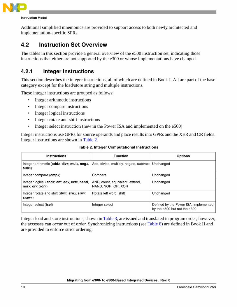
4.2.1 Integer InstructionsThis section describes the integer instructions, all of which are defined in Book I. All are part of the base category except for the load/store string and multiple instructions.
These integer instructions are grouped as follows:
• Integer arithmetic instructions
• Integer compare instructions
• Integer logical instructions
• Integer rotate and shift instructions
• Integer select instruction (new in the Power ISA and implemented on the e500)
Integer instructions use GPRs for source operands and place results into GPRs and the XER and CR fields. Integer instructions are shown in Table 2.
Integer load and store instructions, shown in Table 3, are issued and translated in program order; however, the accesses can occur out of order. Synchronizing instructions (see Table 8) are defined in Book II and are provided to enforce strict ordering.
Table 2. Integer Computational Instructions
Instructions Function Options
Integer arithmetic (addx, divx, mulx, negx, subx)
Add, divide, multiply, negate, subtract Unchanged
Integer compare (cmpx) Compare Unchanged
Integer logical (andx, cnt, eqv, extx, nand, norx, orx, xorx)
AND, count, equivalent, extend, NAND, NOR, OR, XOR
Unchanged
Integer rotate and shift (rlwx, slwx, srwx, srawx)
Rotate left word, shift Unchanged
Integer select (isel) Integer select Defined by the Power ISA, implemented by the e500 but not the e300.

Migrating from e300- to e500-Based Integrated Devices, Rev. 0
Freescale Semiconductor 11
Instruction Model
4.2.2 Floating-Point Instructions (e300)The floating-point model is written to IEEE 754, which defines conventions for single- and double-precision arithmetic. The standard requires that single-precision arithmetic be provided for single-precision operands. (Note that the floating-point instructions are not implemented on the e300c2.)
The signal processing engine (SPE), implemented on the e500v1 and e500v2, defines an alternative floating-point instruction set that uses GPRs rather than FPRs. See Section 3.1.2.1, “SPE Embedded Vector and Scalar Floating-Point Categories.”
Table 4 provides an overview of the floating-point computational instructions.
Table 3. Integer Load/Store Instructions
Instruction Function Comments
Integer load (lbx, lhx, lwx)
Load byte, word, half word, algebraic (half word), byte reverse, and zero, with update, indexed.
Note: The SPE defines instructions for loading and storing double-word operands required for SPE vector instructions and embedded floating-point single-precision vector and double-precision scalar instructions.
Integer load multiple/string word: lmw, lswi
Load multiple word Base category. Implemented on both e300 and e500 cores.
Load string word Move assist category. Implemented on the e300; not implemented on the e500.
Integer store (stbx, sthx, stwx
Store Note: Byte, word, half word, byte-reverse, with update, indexed. The SPE defines instructions for loading and storing double-word operands required for SPE vector instructions and embedded floating-point single-precision vector and double-precision scalar instructions.
Integer store multiple/string word: stmw, stswi
Store multiple word Base category. Implemented on both e300 and e500 cores.
Store string word Move assist category. Implemented on the e300; not implemented on the e500.
Table 4. Floating-Point Computational Instructions
Instructions Instruction Name Comments
Floating-point elementary arithmetic (faddx, fdivx, fmulx, fsubx, fsqrtx, fresx, fabs, fmr, fnabs, fneg)
Add, divide, multiply, reciprocal, square root, subtract, absolute value, move register, negative absolute value, negate
Not one500v1/e500v2
Floating-point multiply-add (fmaddx) Multiply-add, multiply-subtract, negative multiply-add, negative multiply-subtract
Floating-point rounding and conversion (fctix, frx)
Convert to/from integer, round to single-precision
Floating-point compare and select (fcmx) Compare, select
FPSCR (mtfx, mffx) Move to/from FPSCR

Migrating from e300- to e500-Based Integrated Devices, Rev. 0
12 Freescale Semiconductor
Instruction Model
Table 5 shows that the floating-point load and store instructions are required to transfer operands between memory and the FPRs.
4.2.3 Branch and Flow Control Instructions Branch instruction functions include the following:
• Branch instructions redirect instruction execution conditionally based on the value of bits in the CR. For branch conditional instructions, the BO operand specifies the conditions under which the branch is taken.
• CR logical instructions perform logical operations on CR contents that help determine branching conditions.
• Trap instructions test for a specified set of conditions. If any of the tested conditions are met, a system trap type interrupt is taken.
• Executing a System Call (sc) instruction lets a user program call on the system to perform a service by invoking a system call interrupt. System Call instructions can be user- or supervisor-level.
For branch conditional instructions, the BO operand specifies the conditions under which the branch is taken. The BI operand specifies which of the 32 CR bits to test.
All processors support simplified mnemonics that allow conditions specified by BO and BI to be incorporated into the mnemonic. For example, the Branch Conditional instruction, bc BO,BI, target address, can be coded to decrement the count register (CTR) and branch as long as the CTR is not zero (closure of a loop controlled by a count loaded into CTR). To specify this condition, the BO field must be coded as 16. Alternatively, a simplified mnemonic is available, bdnz, that indicates “branch while the decremented value is non-zero.” Using the simplified mnemonic eliminates the BO and BI operands, simplifying ‘bc 16,0,target’ to the more easily remembered ‘bdnz target’, which generates identical machine code.
The supervisor-level rfi instruction is used for returning from a standard interrupt handler.
The differences between the processor families are as follows:
• The rfci instruction, implemented on some e300 devices, is part of the embedded category and is used for critical interrupts on e500 cores.
• The e500 implements the Power ISA–defined rfmci for machine check interrupts. See Section 6, “Interrupt Model.”
Table 5. Floating-Point Load and Store Instructions
Instructions Instruction Name Comments
Floating-point load (lfx) Load floating-point Not on e500v1/e500v2
Floating-point store (stfx) Store floating-point

Migrating from e300- to e500-Based Integrated Devices, Rev. 0
Freescale Semiconductor 13
Instruction Model
Branch and flow control instructions are shown in Table 6.
4.3 Processor Control InstructionsProcessor control instructions are used to read and write registers other than GPRs and FPRs that can be accessed specifically. These include CR, XER, MSR, and SPRs. The time base register and some SPRs are accessible at both the user and supervisor levels; separate SPR numbers are used for each.
Differences between implementations are as follows:
• The e500 implements the Power ISA–defined Write MSR External Enable instructions (wrtee[i]), which updates only MSR[EE] with fewer serialization requirements, and therefore shorter latency, than mtmsr.
Table 7 summarizes processor control instructions.
4.3.1 Memory Synchronization InstructionsMemory synchronization instructions control the order in which memory operations execute with respect to asynchronous events and the order in which operations are seen by other mechanisms that access memory. Differences between processors are highlighted in Table 8.
Table 6. Branch and Flow Control Instructions
Instruction Name Comments
Branch (bx, bcx) Branch Unchanged
CR logical(crx, mcrx)
Condition register Unchanged
Trap (tx, twx) Trap Unchanged
System call (sc) System call Unchanged
Return (rfx) Return from Interrupt, critical, and machine check interrupts.The rfci instruction is defined by the Power ISA but is implemented on the e300.
Table 7. Processor Control Instructions
Instructions Name Comments
Move (mtx, mfx) Move to SPR, CR fields, CR from XER, time base, MSR, PMR
Note: All devices support simplified mnemonics formed by adding the abbreviated name of any SPR to the prefix ‘mf ’, for example mfmas0, mfivor3, and mfcssr1.
Move from SPR, CR fields, CR from XER, time base, MSR, PMR.
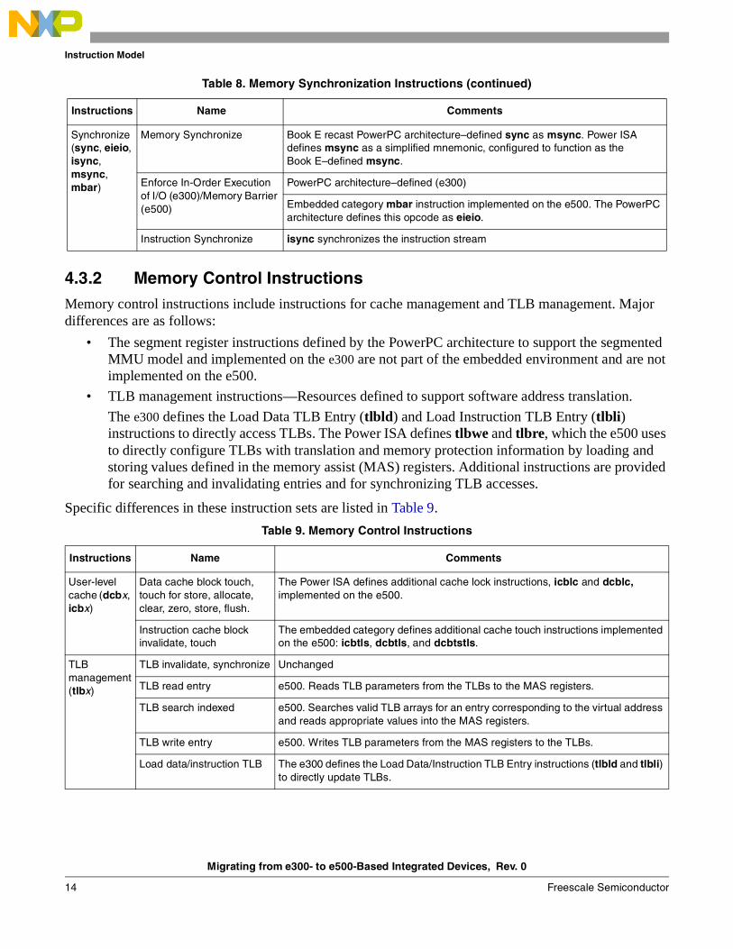
Table 8. Memory Synchronization Instructions
Instructions Name Comments
lwarx Load word and reserve index Unchanged
stwcx. Store word conditional index Unchanged
Migrating from e300- to e500-Based Integrated Devices, Rev. 0
14 Freescale Semiconductor
Instruction Model
4.3.2 Memory Control InstructionsMemory control instructions include instructions for cache management and TLB management. Major differences are as follows:
• The segment register instructions defined by the PowerPC architecture to support the segmented MMU model and implemented on the e300 are not part of the embedded environment and are not implemented on the e500.
• TLB management instructions—Resources defined to support software address translation.
The e300 defines the Load Data TLB Entry (tlbld) and Load Instruction TLB Entry (tlbli) instructions to directly access TLBs. The Power ISA defines tlbwe and tlbre, which the e500 uses to directly configure TLBs with translation and memory protection information by loading and storing values defined in the memory assist (MAS) registers. Additional instructions are provided for searching and invalidating entries and for synchronizing TLB accesses.
Specific differences in these instruction sets are listed in Table 9.
Synchronize(sync, eieio, isync, msync, mbar)
Memory Synchronize Book E recast PowerPC architecture–defined sync as msync. Power ISA defines msync as a simplified mnemonic, configured to function as the Book E–defined msync.
Enforce In-Order Execution of I/O (e300)/Memory Barrier (e500)
PowerPC architecture–defined (e300)
Embedded category mbar instruction implemented on the e500. The PowerPC architecture defines this opcode as eieio.
Instruction Synchronize isync synchronizes the instruction stream
Table 9. Memory Control Instructions
Instructions Name Comments
User-level cache (dcbx, icbx)
Data cache block touch, touch for store, allocate, clear, zero, store, flush.
The Power ISA defines additional cache lock instructions, icblc and dcblc, implemented on the e500.
Instruction cache block invalidate, touch
The embedded category defines additional cache touch instructions implemented on the e500: icbtls, dcbtls, and dcbtstls.
TLBmanagement(tlbx)
TLB invalidate, synchronize Unchanged
TLB read entry e500. Reads TLB parameters from the TLBs to the MAS registers.
TLB search indexed e500. Searches valid TLB arrays for an entry corresponding to the virtual address and reads appropriate values into the MAS registers.
TLB write entry e500. Writes TLB parameters from the MAS registers to the TLBs.
Load data/instruction TLB The e300 defines the Load Data/Instruction TLB Entry instructions (tlbld and tlbli) to directly update TLBs.
Table 8. Memory Synchronization Instructions (continued)
Instructions Name Comments

Migrating from e300- to e500-Based Integrated Devices, Rev. 0
Freescale Semiconductor 15
Instruction Model
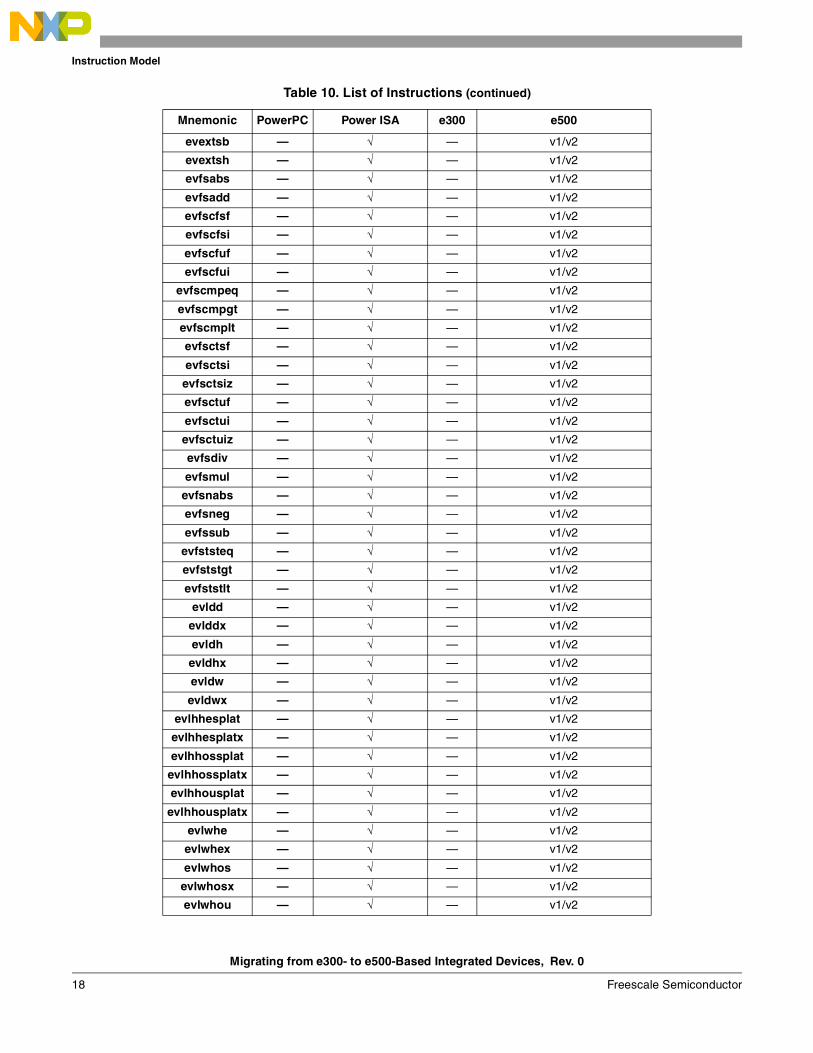
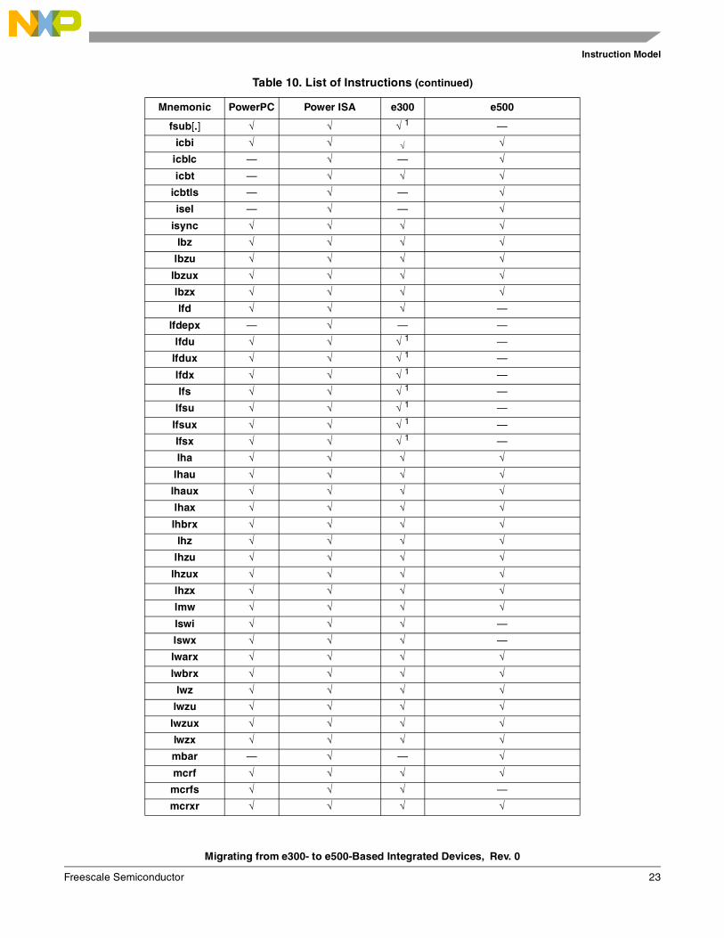
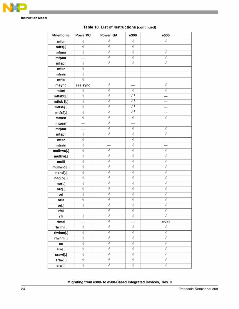
4.3.3 Instruction Set DifferencesTable 10 lists the instructions implemented in the e300 and e500 processors, where applicable, noting the architecture that defines the instruction.
Table 10. List of Instructions
Mnemonic PowerPC Power ISA e300 e500
addc[o][.] √ √ √ √adde[o][.] √ √ √ √
addi √ √ √ √addic[.] √ √ √ √addis √ √ √ √
addme[o][.] √ √ √ √addze[o][.] √ √ √ √
add[o].] √ √ √ √andc[.] √ √ √ √andi. √ √ √ √andis. √ √ √ √and[.] √ √ √ √
b √ √ √ √ba √ √ √ √
bbelr — — — √bblels — — — √
bc √ √ √ √bca √ √ √ √
bcctr √ √ √ √bcctrl √ √ √ √
bcl √ √ √ √bcla √ √ √ √bclr √ √ √ √bclrl √ √ √ √
bl √ √ √ √bla √ √ √ √
brinc — √ — v1/v2
cmp √ √ √ √cmpi √ √ √ √cmpl √ √ √ √cmpli √ √ √ √
cntlzw[.] √ √ √ √crand √ √ √ √crandc √ √ √ √creqv √ √ √ √
crnand √ √ √ √crnor √ √ √ √cror √ √ √ √

Migrating from e300- to e500-Based Integrated Devices, Rev. 0
16 Freescale Semiconductor
Instruction Model
crorc √ √ √ √crxor √ √ √ √dcba √ √ √ √dcbf √ √ √ √dcbi √ √ √ √dcblc — √ — √dcbst √ √ √ √dcbt √ √ √ √
dcbtls — √ — √dcbtst √ √ √ √
dcbtstls — √ — √dcbz √ √ √ √
divwu[o][.] √ √ √ √divw[o][.] √ √ √ √
eciwx √ — — —
ecowx √ — — —
efdabs — √ — v2
efdadd — √ — v2
efdcfs — √ — v2
efdcfsf — √ — v2
efdcfsi — √ — v2
efdcfuf — √ — v2
efdcfui — √ — v2
efdcmpeq — √ — v2
efdcmpgt — √ — v2
efdcmplt — √ — v2
efdctsf — √ — v2
efdctsi — √ — v2
efdctsiz — √ — v2
efdctuf — √ — v2
efdctui — √ — v2
efdctuiz — √ — v2
efddiv — √ — v2
efdmul — √ — v2
efdnabs — √ — v2
efdneg — √ — v2
efdsub — √ — v2
efdtsteq — √ — v2
efdtstgt — √ — v2
efdtstlt — √ — v2
efsabs — √ — v1/v2
efsadd — √ — v1/v2
Table 10. List of Instructions (continued)
Mnemonic PowerPC Power ISA e300 e500

Migrating from e300- to e500-Based Integrated Devices, Rev. 0
Freescale Semiconductor 17
Instruction Model
efscfsf — √ — v1/v2
efscfsi — √ — v1/v2
efscfuf — √ — v1/v2
efscfui — √ — v1/v2
efscmpeq — √ — v1/v2
efscmpgt — √ — v1/v2
efscmplt — √ — v1/v2
efsctsf — √ — v1/v2
efsctsi — √ — v1/v2
efsctsiz — √ — v1/v2
efsctuf — √ — v1/v2
efsctui — √ — v1/v2
efsctuiz — √ — v1/v2
efsdiv — √ — v1/v2
efsmul — √ — v1/v2
efsnabs — √ — v1/v2
efsneg — √ — v1/v2
efssub — √ — v1/v2
efststeq — √ — v1/v2
efststgt — √ — v1/v2
efststlt — √ — v1/v2
eieio √ Replaced with mbar √ mbar
eqv[.] √ √ √ √evabs — √ — v1/v2
evaddiw — √ — v1/v2
evaddsmiaaw — √ — v1/v2
evaddssiaaw — √ — v1/v2
evaddumiaaw — √ — v1/v2
evaddusiaaw — √ — v1/v2
evaddw — √ — v1/v2
evand — √ — v1/v2
evandc — √ — v1/v2
evcmpeq — √ — v1/v2
evcmpgts — √ — v1/v2
evcmpgtu — √ — v1/v2
evcmplts — √ — v1/v2
evcmpltu — √ — v1/v2
evcntlsw — √ — v1/v2
evcntlzw — √ — v1/v2
evdivws — √ — v1/v2
evdivwu — √ — v1/v2
eveqv — √ — v1/v2
Table 10. List of Instructions (continued)
Mnemonic PowerPC Power ISA e300 e500
Migrating from e300- to e500-Based Integrated Devices, Rev. 0
18 Freescale Semiconductor
Instruction Model
evextsb — √ — v1/v2
evextsh — √ — v1/v2
evfsabs — √ — v1/v2
evfsadd — √ — v1/v2
evfscfsf — √ — v1/v2
evfscfsi — √ — v1/v2
evfscfuf — √ — v1/v2
evfscfui — √ — v1/v2
evfscmpeq — √ — v1/v2
evfscmpgt — √ — v1/v2
evfscmplt — √ — v1/v2
evfsctsf — √ — v1/v2
evfsctsi — √ — v1/v2
evfsctsiz — √ — v1/v2
evfsctuf — √ — v1/v2
evfsctui — √ — v1/v2
evfsctuiz — √ — v1/v2
evfsdiv — √ — v1/v2
evfsmul — √ — v1/v2
evfsnabs — √ — v1/v2
evfsneg — √ — v1/v2
evfssub — √ — v1/v2
evfststeq — √ — v1/v2
evfststgt — √ — v1/v2
evfststlt — √ — v1/v2
evldd — √ — v1/v2
evlddx — √ — v1/v2
evldh — √ — v1/v2
evldhx — √ — v1/v2
evldw — √ — v1/v2
evldwx — √ — v1/v2
evlhhesplat — √ — v1/v2
evlhhesplatx — √ — v1/v2
evlhhossplat — √ — v1/v2
evlhhossplatx — √ — v1/v2
evlhhousplat — √ — v1/v2
evlhhousplatx — √ — v1/v2
evlwhe — √ — v1/v2
evlwhex — √ — v1/v2
evlwhos — √ — v1/v2
evlwhosx — √ — v1/v2
evlwhou — √ — v1/v2
Table 10. List of Instructions (continued)
Mnemonic PowerPC Power ISA e300 e500

Migrating from e300- to e500-Based Integrated Devices, Rev. 0
Freescale Semiconductor 19
Instruction Model
evlwhoux — √ — v1/v2
evlwhsplat — √ — v1/v2
evlwhsplatx — √ — v1/v2
evlwwsplat — √ — v1/v2
evlwwsplatx — √ — v1/v2
evmergehi — √ — v1/v2
evmergehilo — √ — v1/v2
evmergelo — √ — v1/v2
evmergelohi — √ — v1/v2
evmhegsmfaa — √ — v1/v2
evmhegsmfan — √ — v1/v2
evmhegsmiaa — √ — v1/v2
evmhegsmian — √ — v1/v2
evmhegumiaa — √ — v1/v2
evmhegumian — √ — v1/v2
evmhesmf — √ — v1/v2
evmhesmfa — √ — v1/v2
evmhesmfaaw — √ — v1/v2
evmhesmfanw — √ — v1/v2
evmhesmi — √ — v1/v2
evmhesmia — √ — v1/v2
evmhesmiaaw — √ — v1/v2
evmhesmianw — √ — v1/v2
evmhessf — √ — v1/v2
evmhessfa — √ — v1/v2
evmhessfaaw — √ — v1/v2
evmhessfanw — √ — v1/v2
evmhessiaaw — √ — v1/v2
evmhessianw — √ — v1/v2
evmheumi — √ — v1/v2
evmheumia — √ — v1/v2
evmheumiaaw — √ — v1/v2
evmheumianw — √ — v1/v2
evmheusiaaw — √ — v1/v2
evmheusianw — √ — v1/v2
evmhogsmfaa — √ — v1/v2
evmhogsmfan — √ — v1/v2
evmhogsmiaa — √ — v1/v2
evmhogsmian — √ — v1/v2
evmhogumiaa — √ — v1/v2
evmhogumian — √ — v1/v2
evmhosmf — √ — v1/v2
Table 10. List of Instructions (continued)
Mnemonic PowerPC Power ISA e300 e500

Migrating from e300- to e500-Based Integrated Devices, Rev. 0
20 Freescale Semiconductor
Instruction Model
evmhosmfa — √ — v1/v2
evmhosmfaaw — √ — v1/v2
evmhosmfanw — √ — v1/v2
evmhosmi — √ — v1/v2
evmhosmia — √ — v1/v2
evmhosmiaaw — √ — v1/v2
evmhosmianw — √ — v1/v2
evmhossf — √ — v1/v2
evmhossfa — √ — v1/v2
evmhossfaaw — √ — v1/v2
evmhossfanw — √ — v1/v2
evmhossiaaw — √ — v1/v2
evmhossianw — √ — v1/v2
evmhoumi — √ — v1/v2
evmhoumia — √ — v1/v2
evmhoumiaaw — √ — v1/v2
evmhoumianw — √ — v1/v2
evmhousiaaw — √ — v1/v2
evmhousianw — √ — v1/v2
evmra — √ — v1/v2
evmwhsmf — √ — v1/v2
evmwhsmfa — √ — v1/v2
evmwhsmi — √ — v1/v2
evmwhsmia — √ — v1/v2
evmwhssf — √ — v1/v2
evmwhssfa — √ — v1/v2
evmwhumi — √ — v1/v2
evmwhumia — √ — v1/v2
evmwlsmiaaw — √ — v1/v2
evmwlsmianw — √ — v1/v2
evmwlssiaaw — √ — v1/v2
evmwlssianw — √ — v1/v2
evmwlumi — √ — v1/v2
evmwlumia — √ — v1/v2
evmwlumiaaw — √ — v1/v2
evmwlumianw — √ — v1/v2
evmwlusiaaw — √ — v1/v2
evmwlusianw — √ — v1/v2
evmwsmf — √ — v1/v2
evmwsmfa — √ — v1/v2
evmwsmfaa — √ — v1/v2
evmwsmfan — √ — v1/v2
Table 10. List of Instructions (continued)
Mnemonic PowerPC Power ISA e300 e500

Migrating from e300- to e500-Based Integrated Devices, Rev. 0
Freescale Semiconductor 21
Instruction Model
evmwsmi — √ — v1/v2
evmwsmia — √ — v1/v2
evmwsmiaa — √ — v1/v2
evmwsmian — √ — v1/v2
evmwssf — √ — v1/v2
evmwssfa — √ — v1/v2
evmwssfaa — √ — v1/v2
evmwssfan — √ — v1/v2
evmwumi — √ — v1/v2
evmwumia — √ — v1/v2
evmwumiaa — √ — v1/v2
evmwumian — √ — v1/v2
evnand — √ — v1/v2
evneg — √ — v1/v2
evnor — √ — v1/v2
evor — √ — v1/v2
evorc — √ — v1/v2
evrlw — √ — v1/v2
evrlwi — √ — v1/v2
evrndw — √ — v1/v2
evsel — √ — v1/v2
evslw — √ — v1/v2
evslwi — √ — v1/v2
evsplatfi — √ — v1/v2
evsplati — √ — v1/v2
evsrwis — √ — v1/v2
evsrwiu — √ — v1/v2
evsrws — √ — v1/v2
evsrwu — √ — v1/v2
evstdd — √ — v1/v2
evstddx — √ — v1/v2
evstdh — √ — v1/v2
evstdhx — √ — v1/v2
evstdw — √ — v1/v2
evstdwx — √ — v1/v2
evstwhe — √ — v1/v2
evstwhex — √ — v1/v2
evstwho — √ — v1/v2
evstwhox — √ — v1/v2
evstwwex — √ — v1/v2
evstwwex — √ — v1/v2
evstwwo — √ — v1/v2
Table 10. List of Instructions (continued)
Mnemonic PowerPC Power ISA e300 e500

Migrating from e300- to e500-Based Integrated Devices, Rev. 0
22 Freescale Semiconductor
Instruction Model
evstwwox — √ — v1/v2
evsubfsmiaaw — √ — v1/v2
evsubfssiaaw — √ — v1/v2
evsubfumiaaw — √ — v1/v2
evsubfusiaaw — √ — v1/v2
evsubfw — √ — v1/v2
evsubifw — √ — v1/v2
evxor — √ — v1/v2
extsb[.] √ √ √ √extsh[.] √ √ √ √fabs[.] √ √ √ 1 —
fadds[.] √ √ √ 1 —
fadd[.] √ √ √ 1 —
fcfid[.] √ √ √ 1 —
fcmpo √ √ √ 1 —
fcmpu √ √ √ 1 —
fctidz[.] √ √ √ 1 —
fctid[.] √ √ √ 1 —
fctiwz[.] √ √ √ 1 —
fctiw[.] √ √ √ 1 —
fdivs[.] √ √ √ 1 —
fdiv[.] √ √ √ 1 —
fmadds[.] √ √ √ 1 —
fmadd[.] √ √ √ 1 —
fmr[.] √ √ √ 1 —
fmsubs[.] √ √ √ 1 —
fmsub[.] √ √ √ 1 —
fmuls[.] √ √ √ 1 —
fmul[.] √ √ √ 1 —
fnabs[.] √ √ √ 1 —
fneg[.] √ √ √ 1 —
fnmadds[.] √ √ √ 1 —
fnmadd[.] √ √ √ 1 —
fnmsubs[.] √ √ √ 1 —
fnmsub[.] √ √ √ 1 —
fres[.] √ √ √ 1 —
frsp[.] √ √ √ 1 —
frsqrte[.] √ √ √ 1 —
fsel[.] √ √ √ 1 —
fsqrts[.] √ √ √ 1 —
fsqrt[.] √ √ √ 1 —
fsubs[.] √ √ √ 1 —
Table 10. List of Instructions (continued)
Mnemonic PowerPC Power ISA e300 e500
Migrating from e300- to e500-Based Integrated Devices, Rev. 0
Freescale Semiconductor 23
Instruction Model
fsub[.] √ √ √ 1 —
icbi √ √ √ √icblc — √ — √icbt — √ √ √
icbtls — √ — √isel — √ — √
isync √ √ √ √lbz √ √ √ √
lbzu √ √ √ √lbzux √ √ √ √lbzx √ √ √ √lfd √ √ √ —
lfdepx — √ — —
lfdu √ √ √ 1 —
lfdux √ √ √ 1 —
lfdx √ √ √ 1 —
lfs √ √ √ 1 —
lfsu √ √ √ 1 —
lfsux √ √ √ 1 —
lfsx √ √ √ 1 —
lha √ √ √ √lhau √ √ √ √lhaux √ √ √ √lhax √ √ √ √lhbrx √ √ √ √lhz √ √ √ √
lhzu √ √ √ √lhzux √ √ √ √lhzx √ √ √ √lmw √ √ √ √lswi √ √ √ —
lswx √ √ √ —
lwarx √ √ √ √lwbrx √ √ √ √lwz √ √ √ √
lwzu √ √ √ √lwzux √ √ √ √lwzx √ √ √ √mbar — √ — √mcrf √ √ √ √mcrfs √ √ √ —
mcrxr √ √ √ √
Table 10. List of Instructions (continued)
Mnemonic PowerPC Power ISA e300 e500
Migrating from e300- to e500-Based Integrated Devices, Rev. 0
24 Freescale Semiconductor
Instruction Model
mfcr √ √ √ √mffs[.] √ √ √mfmsr √ √ √ √mfpmr — √ √ √mfspr √ √ √ √mfsr √
mfsrin √mftb √
msync see sync √ — √mtcrf √ √ √ √
mtfsb0[.] √ √ √ 1 —
mtfsb1[.] √ √ √ 1 —
mtfsfi[.] √ √ √ 1 —
mtfsf[.] √ √ √ 1 —
mtmsr √ √ √ √mtocrf — √ —
mtpmr — √ √ √mtspr √ √ √ √mtsr √ — √ —
mtsrin √ — √ —
mulhwu[.] √ √ √ √mulhw[.] √ √ √ √
mulli √ √ √ √mullw[o][.] √ √ √ √
nand[.] √ √ √ √neg[o][.] √ √ √ √
nor[.] √ √ √ √orc[.] √ √ √ √ori √ √ √ √oris √ √ √ √or[.] √ √ √ √rfci — √ √ √rfi √ √ √ √
rfmci — √ — e500
rlwimi[.] √ √ √ √rlwinm[.] √ √ √ √rlwnm[.] √ √ √ √
sc √ √ √ √slw[.] √ √ √ √
srawi[.] √ √ √ √sraw[.] √ √ √ √srw[.] √ √ √ √
Table 10. List of Instructions (continued)
Mnemonic PowerPC Power ISA e300 e500

Migrating from e300- to e500-Based Integrated Devices, Rev. 0
Freescale Semiconductor 25
Instruction Model
stb √ √ √ √stbu √ √ √ √
stbux √ √ √ √stbx √ √ √ √stfd √ √ √
stfdu √ √ √ 1 —
stfdux √ √ √ 1 —
stfdx √ √ √ 1 —
stfiwx √ √ √ 1 —
stfs √ √ √ 1 —
stfsu √ √ √ 1 —
stfsux √ √ √ 1 —
stfsx √ √ √ 1 —
sth √ √ √ √sthbrx √ √ √ √sthu √ √ √ √sthux √ √ √ √sthx √ √ √ √stmw √ √ √ √stswi √ √ √ —
stswx √ √ √ —
stw √ √ √ √stwbrx √ √ √ √stwcx. √ √ √ √stwu √ √ √ √stwux √ √ √ √stwx √ √ √ √
subfc[o][.] √ √ √ √subfe[o][.] √ √ √ √
subfic √ √ √ √subfme[o][.] √ √ √ √subfze[o][.] √ √ √ √subf[o][.] √ √ √ √
sync √ msync √ See Section 4.3.1, on page 13
tlbia √ — √ —
tlbie √ — √ —
tlbivax — √ — √tlbld — — √ —
tlbli — — √ —
tlbre — √ — √tlbsx √ √ √
tlbsync √ √ √ √
Table 10. List of Instructions (continued)
Mnemonic PowerPC Power ISA e300 e500
Migrating from e300- to e500-Based Integrated Devices, Rev. 0
26 Freescale Semiconductor
Register Model
5 Register ModelMost registers defined in the PowerPC architecture are unchanged in the e500 implementation of the Power Architecture model. A few have been replaced by other registers, and in some cases new fields are added, primarily to support functionality defined by categories that have been added to the architecture. Differences include the following:
• Bit numbering. 32-bit registers in the PowerPC architecture (e300) are numbered 0–31; the same registers in Power ISA (e500) are numbered 32–63. Any 32-bit registers that are defined as 64-bit registers in the Power ISA are treated as the lower word of the 64-bit versions. These include the GPRs, save/restore registers, and all registers that can hold addresses (such as the count and link registers).
• Register files. These sets of registers hold operands for computational, load, and store instructions. The architecture defines the following register files:
— General-purpose registers (GPRs). All cores implement GPRs.
The SPE uses the 32-bit GPRs extended to 64-bits. GPRs are often used to generate the effective address for instructions that access memory (because GPRs are used to hold addresses, 64-bit implementations require 64-bit GPRs). The e300 cores implement 32-bit GPRs. On the e300, these bits are numbered 0–31.
See Section 5.1, “Register File Comparison.”
— Floating-point registers (FPRs). All cores that support the Power Architecture model base category floating-point instructions implement the FPRs, but the e500v1 and e500v2 do not.
• Instruction-accessible registers—Registers such as the condition register (CR), the floating-point status and control register (FPSCR), and some SPRs are accessed as side effects of executing certain instructions. All processors implement CRs, but processors that do not support FPRs also do not support the FPSCRs or floating-point functionality defined in the CR.
• Special-purpose registers (SPRs)—On-chip registers that are part of the processor core. Although the basic set of SPRs is implemented across all cores, some SPRs may not be implemented on all cores, or may have different meanings relative to the core or to the device into which the core is integrated. Always check the register summary chapter in the SoC reference manual for the most specific information.
tlbwe — √ — √tw √ √ √ √twi √ √ √ √
wrtee — √ — √wrteei — √ — √xori[.] √ √ √ √xor[.] √ √ √ √
1 (Not including e300c2)
Table 10. List of Instructions (continued)
Mnemonic PowerPC Power ISA e300 e500
Migrating from e300- to e500-Based Integrated Devices, Rev. 0
Freescale Semiconductor 27
Register Model
Cores also include both the architecture-defined and implementation-specific SPRs required for the functionality provided. These differences are summarized at the register level in the comparison tables in the subsequent sections. Specific details are provided in the reference manuals for the cores and the integrated devices.
NOTEPerformance monitor registers, or PMRs, offer an extensive set of on-chip registers similar to SPRs. These are defined by the Power ISA and implemented on the e500 and are implementation-specific resources on e300 cores.
To optimize instruction execution, implementations typically employ duplicate space for certain heavily used registers, such as rename and shadow registers. Such microarchitectural resources vary from device to device and are not addressed here.
5.1 Register File ComparisonFigure 3 compares register files. Note that, as the GPRs in Figure 3 illustrate, bit numbering for 32-bit registers differs between the PowerPC architecture and the Power Architecture model.
Architecture-defined register files shown in Figure 3 are defined as follows:
• General-purpose registers (GPRs)—GPRs serve as the data source or destination for all integer and non–floating-point load/store instructions and provide data for generating addresses. The GPR file consists of 32 GPRs designated as GPR0–GPR31.
The e300 implements 32-bit GPRs with bits numbered 0–31.
The SPE, implemented on e500v1 and e500v2 cores, extends the GPRs to accommodate 64-bit operands; scalar double-precision embedded floating-point instructions treat the 64 bits as a single operand; SPE vector instructions break the registers into two 32-bit elements, which for some instructions are broken into half-word elements.
e300 e500
0 31 0 31 32 63
GPR0
General-purposeregisters
(upper) GPR0 (lower)
General-purpose registers (The base category defines only the lower half (bits 32–63)).
e500v1/e500v2
GPR1 GPR1
GPR2 GPR2
• • • • • •GPR31 GPR31
The SPE defines the upper 32 bits for use with 64-bit operands
0 63
Floating-pointregisters(not including the e300c2)
FPR0
FPR1
FPR2
• • •FPR31
Figure 3. Register File Comparison

Migrating from e300- to e500-Based Integrated Devices, Rev. 0
28 Freescale Semiconductor
Register Model
• Floating-point registers (FPRs)—The floating-point model defines an FPR file that consists of thirty-two 64-bit FPRs, FPR0–FPR31. The FPRs use double-precision operand format for both single- and double-precision data. See Section 4.2.2, “Floating-Point Instructions (e300).”
5.2 Instruction-Accessible RegistersFigure 4 shows a comparison of registers that may be updated as the by-product of instruction execution. For example, an overflow may update the condition register (CR), the floating-point status and control register (FPSCR), or the SPE/embedded floating-point status and control register (SPEFSCR). For some of these registers, such as the FPSCR and CR, explicit move to/move from instructions are defined to explicitly access these registers.
The differences in these register sets depend on whether SPE and floating-point instructions are supported.
The following e500 registers support SPE and embedded floating-point instructions:
• SPE floating-point status and control register (SPEFSCR). Used for status and control of SPE and embedded floating-point instructions. It controls the handling of floating-point exceptions and records status information resulting from the floating-point operations.
• Accumulator register (ACC). Holds the results of the multiply accumulate (MAC) forms of SPE integer instructions. The ACC allows back-to-back execution of dependent MAC instructions, something that is found in the inner loops of DSP code such as finite impulse response (FIR) filters. The accumulator is partially visible to the programmer in that its results do not have to be explicitly read to use them. Instead, they are always copied into a 64-bit destination GPR specified as part of the instruction. Based upon the type of instruction, this register can hold either a single 64-bit value or a vector of two 32-bit elements.
e300 e500
0 31 0 31 32 63
CR Condition register CR Condition register
Base categoryspr 1 XER Integer exception register spr 1 XER Integer exception register
spr 8 LR Link register spr 8 LR Link register; ;
spr 9 CTR Count register spr 9 CTR Count register
FPSCR Floating-point status/control (not e300c2)
spr 512 SPEFSCR SPE FP status and control SPE: e500
ACC Accumulator
Figure 4. Instruction-Accessible Registers Comparison

Migrating from e300- to e500-Based Integrated Devices, Rev. 0
Freescale Semiconductor 29
Register Model
5.3 Timer Register ComparisonFigure 5 shows a comparison of timer-related registers.
Both families implement the following registers:
• Time base (TBU and TBL). Provides timing functions for the system.
• Decrementer register (DEC). Typically used as a general-purpose software timer. It is updated at the same rate as the TB and provides a way to signal a decrementer, fixed-interval timer, or watchdog timer interrupt after a specified period.
The e500 implements Power ISA–defined registers that incorporate timing mechanisms for the fixed-interval and watchdog timer interrupts:
• Decrementer auto-reload register (DECAR). Can be used to automatically reload a programmed value into DEC. If DECAR is not used, a value has to be explicitly programmed into the DEC, as in the PowerPC architecture.
• Timer control register (TCR). Provides control information for the decrementer. It controls features such as auto-reload enable and decrementer interrupt enable.
• Timer status register (TSR). Contains status on timer events and the most recent watchdog timer-initiated processor reset. It controls features such as watchdog timer, fixed-interval interrupt enable, and watchdog timer interrupt status.
• The alternate time base registers duplicate much of the functionality of the time base, but do not support the DECAR. The alternate time base is typically clocked at a higher frequency than the standard time base to offer a finer granularity.
e300 e500
0 31 32 63
spr 268 TBL User-level time base lower/upper(read-only)
spr 268 TBL User-level time base lower/upper (read-only)
Base category
spr 269 TBU spr 269 TBU
spr 284 TBL Supervisor-level time base lower/upper
spr 284 TBL Supervisor-level time base lower/upper spr 285 TBU spr 285 TBU
spr 22 DEC Decrementer spr 22 DEC Decrementer
spr 54 DECAR Decrementer auto-reload
Embedded category spr 340 TCR Timer control
spr 336 TSR Timer status
spr 526 ATBL Alternate time base lower/upper Alternate time-base
spr 527 ATBU
Figure 5. Time/Decrementer Registers Comparison

Migrating from e300- to e500-Based Integrated Devices, Rev. 0
30 Freescale Semiconductor
Register Model
5.4 MMU Control and Status Register ComparisonBecause the original PowerPC architecture MMU specification was cumbersome for embedded applications, both the e300 and e500 defined alternate features, especially to support software-managed page tables. Both the e300 and e500 MMUs differ from the model defined in the PowerPC Book III. On the e300, these extensions are implementation specific, whereas the e500 memory model is defined by Book III-e. See Section 7, “Memory Management Unit (MMU) Model.”
Figure 6 compares the MMU registers.
e300 e500
a MMU Control and Status (Read/Write)0 31 32 63
spr 528 IBAT0U
Instruction block-address translation registers
spr 48 PID0Process IDregisters 0–2
Embedded category
spr 529 IBAT0L spr 633 PID1e500v1/e500v2
• • • spr 634 PID2
spr 534 IBAT3U MMU control and status register 0spr 1012 MMUCSR0
spr 535 IBAT3L
spr 624 MAS0
MMU assist registers 0–4 and 6
spr 536 DBAT0U
Data block-addresstranslation registers
spr 625 MAS1spr 537 DBAT0L
spr 626 MAS2• • •
Embedded categoryspr 627 MAS3spr 542 DBAT3U
spr 628 MAS4spr 543 DBAT3L
spr 630 MAS6
SR0
Segment registers
spr 944 MAS7 e500v2
SR1 MMU Control and Status (Read Only)
SR2
• • • spr 1015 MMUCFG MMU configuration
SR31 spr 688 TLB0CFG
TLB configuration 0/1 spr 25 SDR1 SDR1 spr 689 TLB1CFG
spr 560 IBAT4U
Instruction block-address translation registers
spr 561 IBAT4L
• • •
spr 566 IBAT7U
spr 567 IBAT7L
spr 568 DBAT4U
Data block-addresstranslation registers
spr 569 DBAT4L
• • •
spr 574 DBAT7U
spr 575 DBAT7L
e300–specific
Figure 6. MMU Register Comparison
spr 978 DMISSData and instruction miss
spr 979 IMISS
spr 976 HASH1 Primary and secondary hash spr 980 HASH2
spr 977 DCMP Data/instruction TLB comparespr 981 ICMP
spr 882 RPA Required physical address
Migrating from e300- to e500-Based Integrated Devices, Rev. 0
Freescale Semiconductor 31
Register Model
The e300 cores implement the following MMU registers defined by the PowerPC architecture, but not supported by the Power ISA embedded cores:
• Block address translation registers (BATs).
• SDR1
The e300 implements the following implementation-specific registers, which are not implemented on the e500:
• Instruction and data TLB miss address registers (IMISS and DMISS). When a TLB miss interrupt occurs, the IMISS or DMISS register contains the 32-bit effective address of the instruction or data access, respectively, that caused the miss.
• Primary and secondary hash address registers (HASH1 and HASH2). Contain the primary and secondary PTEG addresses that correspond to the address causing a TLB miss. These addresses are derived automatically by the core by performing the primary and secondary hashing function on the contents of IMISS or DMISS, for an ITLB or DTLB miss interrupt, respectively.
• Instruction and data PTE compare registers (ICMP and DCMP). Contain the word to be compared with the first word of a PTE in the table search software routine to determine if a PTE contains the address translation for the instruction or data access. The ICMP and DCMP contents are automatically derived by the core when a TLB miss interrupt occurs.
• Required physical address register (RPA). The system software loads a TLB entry by loading the second word of the matching PTE entry into the RPA register and then executing the tlbli or tlbld instruction (for loading the ITLB or DTLB, respectively).
The e500 implements the following Power ISA–defined SPRs to support address translation:
• Process ID registers (PID0–PID2). Provides an identifier value associated with each effective address (instruction or data) generated by the processor. The Power ISA supports as many as 16 PIDs.
• MMU control and status register 0 (MMUCSR0). Used for general MMU control, for example, to invalidate TLBs.
• MMU assist (MAS) registers. Used with the tlbwe and tlbre instructions to configure and manage MMU read/write and replacement, descriptor configuration, effective page number and page attributes, real page number and access, and hardware replacement assist configuration.
• MMU configuration register (MMUCFG). Provides configuration information for the particular MMU supplied with a version of the core. It is a read-only register that provides information on PID register size and the number of TLBs.
• TLB configuration registers (TLB0CFG–TLB1CFG). These read-only registers provide information about each TLB that is visible to the programming model. They provide configuration information for TLBs and describe aspects such as the associativity, minimum and maximum page sizes of the TLBs, and the number of entries in the TLBs.

Migrating from e300- to e500-Based Integrated Devices, Rev. 0
32 Freescale Semiconductor
Register Model
5.5 Cache Register Comparison The Freescale EIS defines the e500 L1 cache configuration and status registers, shown in Figure 7. Neither version of the architecture defines cache registers.
The e500 registers in Figure 7 are described as follows:
• L1 cache configuration registers (L1CFG0–L1CFG1). Read-only registers that provide configuration information for the particular L1 data and instruction caches supplied with a version of the core. They include a description of the cache block size, the number of ways, the cache size, and the cache replacement policy, among other features.
• L1 cache control and status registers (L1CSR0–L1CSR1). L1CSRs are used for general control and status of the L1 data and instruction caches and are read/write accessible by supervisor-level programs. They allow the programmer to enable features such as cache parity and the cache itself. They provide status on information such as cache locking and cache locking overflow.
The e300 implements the following L1 cache control bits in HID0:
• Instruction/data cache enable (ICE/DCE). Clearing the bit disables the cache; it can be neither accessed nor updated. Potential cache accesses from the bus (snoop and cache operations) are ignored and bL1 cache tag state bits are ignored and all instruction fetches are propagated to the coherent system bus (CSB) as single-beat or burst transactions, depending on the value of HID2[IFEB]. oth caches are disabled at reset.
• Data/instruction cache lock (DLOCK/ILOCK). If this bit is set, all ways of the respective cache are locked. A locked cache supplies data normally on a hit, but is treated as a cache-inhibited transaction on a miss. The e500 implements the cache locking instructions listed in Section 4.3.2, “Memory Control Instructions.”
• Instruction/data cache flash invalidate (ICFI/DCFI). Setting this bit generates an invalidate operation that marks the state of each instruction cache block as invalid. Setting ICFI clears all the valid bits of the blocks and the PLRU bits to point to way L0 of each set.
The e300 HID2 register includes the following:
• Cache way locking fields (IWLCK, DWLCK)
• Instruction cache way protection (ICWP). Used to protect locked ways in the instruction cache from being invalidated.
See the core and SoC reference manuals for details about fields within these registers.
e300 e500
e300 cores do not implement cache management registers, but provide cache locking and enablement in the HID registers, as
described below.
L1 Cache (Read/Write)32 63
spr 1010 L1CSR0L1 cache control/status 0/1
spr 1011 L1CSR1
L1 Cache (Read Only)
spr 515 L1CFG0L1 cache control/status 0/1
spr 516 L1CFG1
Figure 7. Cache Registers Comparison

Migrating from e300- to e500-Based Integrated Devices, Rev. 0
Freescale Semiconductor 33
Register Model
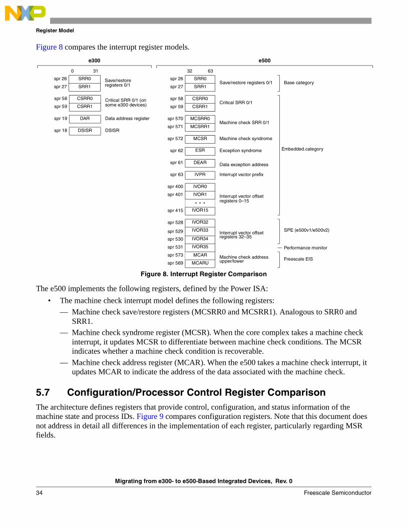
5.6 Interrupt Register ComparisonThe Power ISA embedded category optimizes the architected resources to improve responsiveness to interrupts, especially for asynchronous interrupts signaled to the core from peripheral logic within the SoC. As Figure 8 shows, these differences include the following:
• In the PowerPC architecture which is implemented on the e300, an interrupt vector consists of a fixed offset prepended with a value as determined by MSR[IP], which is not part of the Power ISA. On e500 cores, these offsets are programmed through the interrupt vector prefix register (IVPR), which places the interrupt table in memory, and the interrupt vector offset registers (IVORs), which contain the offset for individual interrupts.
IVORs hold the index from the base address provided by the IVPR for its respective interrupt type. IVORs provide storage for specific interrupts. The Power ISA definition allows implementations to define IVORs to support category- and implementation-specific interrupts. For example, the SPE defines IVOR32–IVOR35. Such IVORs are listed at the bottom of Table 11.
• To manage the increased traffic from peripheral devices, the Power ISA provides analogous resources for critical input interrupt with its own set of save and restore registers. This functionality also exists as implementation-specific functionality in some cores. The Power ISA defines similar resources for machine check interrupts implemented on e500 cores.
• Support for data related interrupts has changed, as follows:
— The e500 implements the exception syndrome register (ESR) instead of the DSI syndrome register (DSISR). The DSISR is used for data storage and alignment interrupts. The ESR is used to track exceptions for a variety of interrupts.
— The e500 implements the data exception address register (DEAR). DEAR is loaded with the effective address of a data access (caused by a load, store, or cache management instruction) that results in an alignment, data TLB miss, or DSI exception. The e300 implements the data address register (DAR) for this purpose.
Migrating from e300- to e500-Based Integrated Devices, Rev. 0
34 Freescale Semiconductor
Register Model
Figure 8 compares the interrupt register models.
The e500 implements the following registers, defined by the Power ISA:
• The machine check interrupt model defines the following registers:
— Machine check save/restore registers (MCSRR0 and MCSRR1). Analogous to SRR0 and SRR1.
— Machine check syndrome register (MCSR). When the core complex takes a machine check interrupt, it updates MCSR to differentiate between machine check conditions. The MCSR indicates whether a machine check condition is recoverable.
— Machine check address register (MCAR). When the e500 takes a machine check interrupt, it updates MCAR to indicate the address of the data associated with the machine check.
5.7 Configuration/Processor Control Register Comparison The architecture defines registers that provide control, configuration, and status information of the machine state and process IDs. Figure 9 compares configuration registers. Note that this document does not address in detail all differences in the implementation of each register, particularly regarding MSR fields.
e300 e500
0 31 32 63
spr 26 SRR0 Save/restoreregisters 0/1
spr 26 SRR0Save/restore registers 0/1 Base category
spr 27 SRR1 spr 27 SRR1
spr 58 CSRR0Critical SRR 0/1
Embedded.category
spr 59 CSRR1
spr 570 MCSRR0Machine check SRR 0/1
spr 571 MCSRR1
spr 572 MCSR Machine check syndrome
spr 62 ESR Exception syndrome
spr 61 DEAR Data exception address
spr 63 IVPR Interrupt vector prefix
spr 400 IVOR0
Interrupt vector offset registers 0–15
spr 401 IVOR1
• • •
spr 415 IVOR15
spr 528 IVOR32
Interrupt vector offset registers 32–35
SPE (e500v1/e500v2)spr 529 IVOR33
spr 530 IVOR34
spr 531 IVOR35 Performance monitor
spr 573 MCAR Machine check address upper/lower Freescale EIS
spr 569 MCARU
Figure 8. Interrupt Register Comparison
spr 58 CSRR0 Critical SRR 0/1 (on some e300 devices) spr 59 CSRR1
spr 19 DAR Data address register
spr 18 DSISR DSISR

Migrating from e300- to e500-Based Integrated Devices, Rev. 0
Freescale Semiconductor 35
Register Model
• Machine state register (MSR). Defines the state of the processor (that is, enabling and disabling of interrupts and debugging exceptions, enabling and disabling some features, and specifying whether the processor is in supervisor or user mode).
The PowerPC architecture MSR (e300) defines bits that enable data address translation (IR and DR) and modal big/little endian byte ordering (LE and ILE). On the e500 byte ordering is a page attribute configured through the MAS registers.
The MSR includes bits for enabling and disabling asynchronous interrupts: EE for external interrupts, CE for critical interrupts, and ME for machine check interrupts. The core user documentation describes the behavior of these bits when the respective interrupt is taken and how they should be treated by the interrupt handler. Note also that the Power ISA implements the Write MSR External Enable instructions (wrtee[i]), which can be used to update only MSR[EE].
MSR[LE] and MSR[ILE] on the e300are used to set configure the big- and true little-endian byte ordering; these are not implemented on the e500 and other Power ISA devices, which handle endianness on a per-page basis through the MAS registers.
The MSR[IP] value places the interrupt table in either high or low memory. This is not implemented on the e500, which uses IVPR and the IVORs to define the interrupt table and place it in memory.
• Processor ID register (PIR). Contains a value that can be used to distinguish the processor from other processors in the system. Note that the PowerPC architecture and Power ISA PIR SPR numbers differ.
• Processor version register (PVR). Contains a value identifying the version and revision level of the processor. The PVR distinguishes between processors whose attributes may affect software.
• The system version register (SVR) identifies the integrated device that implements the core.
5.8 Performance Monitor Register ComparisonThe e300c3, e300c4, and e500 cores’ performance monitor utility uses the set of registers shown in Figure 10. The e300 and e500 processors implement this functionality in performance monitor registers (PMRs), which are part of the Power ISA. PMRs are similar to the SPRs and are accessed by mtpmr and mfpmr instructions.
The counter registers, global controls, and local controls have alias names and use different PMR numbers. Accesses to PMC0–PMC15, PMGC0, PMLCa0–PMLCa15, and PMLCb0–PMLCb15 use the
e300 e500
0 31 32 63
MSR Machine state MSR Machine state
Base categoryspr 287 PVR Processor version spr 287 PVR Processor version
spr 286 1 SVR System version (e300-specific) spr 1023 1 SVR System version
spr 286 1 PIR Processor ID Freescale EIS
1 Note that the SVR is SPR 1023 on the e500 and SPR 286 on the e300. The PIR is SPR 286 on the e500.
Figure 9. Configuration Registers Comparison

Migrating from e300- to e500-Based Integrated Devices, Rev. 0
36 Freescale Semiconductor
Register Model
supervisor-level PMR number; accesses to UPMC0–UPMC15, UPMGC0, UPMLCa0–UPMLCa15, and UPMLCb0–UPMLCb15 use the user-level PMR number. User-level access is read only.
It is important to note that the events counted can differ greatly among processors; consult the user documentation. Also note that most integrated devices implement a similar performance monitor that tracks events mostly involving peripheral device activities. These events may trigger an asynchronous interrupt, typically configured as an external interrupt.
5.9 Debug Register ComparisonDebug registers are accessible to software running on the processor. These registers are intended for use by special debug tools and debug software, and not by general application or operating system code. Figure 11 compares debug registers.
The Power ISA does not implement data address breakpoint registers (DABRs) nor instruction address breakpoint registers (IABRs), but instead architects debugging support with the following registers:
• Debug control registers (DBCR0–DBCR1). Enable debug events, reset the processor, control timer operation during debug events, and set the debug mode of the processor.
e300c3, e300c4, and e500
User PMRs (Read-Only)
32 63
pmr 384 [U]PMGC0 Global control register
pmr 0–3 [U]PMC0–3 Counter registers 0–3
pmr 128–131 [U]PMLCa0–3 Local control registers a0–a3
pmr 256–259 [U]PMLCb0–3 Local control registers b0–b3
Supervisor PMRs
pmr 400 PMGC0 Global control register
pmr 16–19 PMC0–3 Counter registers 0–3
pmr 144–147 PMLCa0–3 Local control a0–a3
pmr 272–275 PMLCb0–3 Local control b0–b3
Figure 10. Performance Monitor Registers Comparison
e300 e500
0 31 32 63
spr 308 DBCR0
Debug control registers 0–2spr 309 DBCR1
spr 310 DBCR2
spr 304 DBSR Debug status register
spr 312 IAC1 Instruction address compareregisters 1 and 2spr 313 IAC2
spr 316 DAC1 Data address compare registers 1 and 2spr 317 DAC2
Figure 11. Debug Registers Comparison
spr 1013 DABR Data address breakpoint
spr 317 DABR2 Data address breakpoint 2
spr 1010 IABR Instruction address breakpoint
spr 1018 IABR2 Instruction address breakpoint 2
spr 309 IBCRInstruction/data breakpoint control
spr 310 DBCR

Migrating from e300- to e500-Based Integrated Devices, Rev. 0
Freescale Semiconductor 37
Register Model
• Debug status register (DBSR). Provides status information for debug events and for the most recent processor reset. The DBSR is set through hardware but is read and cleared through software.
• Instruction and data address compare registers (IACs and DACs). A debug event may be enabled to occur on an attempt to execute an instruction or access a data location from an address specified in an IAC or DAC, inside or outside a range specified by the IAC or DAC, or to blocks of addresses specified by the combination of the IACs and DACs.
• Note that additional enhanced embedded debug interrupt resources are described in Section 5.6, “Interrupt Register Comparison.”
5.10 Software-Use SPR ComparisonSoftware-use SPRs (SPRGs), shown in Figure 12, have no defined functionality, although many are added to the register set in conjunction with other functionality, for example the Freescale MMU architecture.
SPRGs consist of the following supervisor-level read/write registers:
• SPRG0–SPRG3—defined in both versions of the architecture.
• SPRG4–SPRG7—implementation-specific registers implemented on e300 cores, and also defined by the Power ISA.
On the e300, SPRGs are all supervisor-only, read/write registers. e500 SPRGs are defined by the Power ISA as follows:
• SPRG0–SPRG2—accessible only in supervisor mode.
• SPRG3—write-only in supervisor mode. It is readable in supervisor mode, but whether it can be read in user mode is implementation-dependent. Note that, as Figure 12 shows, the SPR numbers differ for user and supervisor accesses.
• SPRG4–SPRG7—write-only in supervisor mode but readable in supervisor or user mode. Note that, as Figure 12 shows, the SPR numbers differ for user and supervisor accesses.
• USPRG0—can be accessed in supervisor or user mode. Note that USPRG0 is a separate physical register from SPRG0.
e300 e500
Supervisor SPRGs User SPRGs
Architecture-Defined General SPRs (Read-Only)
0 31 32 63
spr 272 SPRG0
SPR general registers 0–3
spr 259 SPRG3
SPR general registers 3–7spr 273 SPRG1 spr 260 SPRG4
spr 274 SPRG2 • • •
spr 275 SPRG3 spr 263 SPRG7
e300-Specific User SPRGs (Read/Write)
spr 276 SPRG4
SPR general registers 4–7
spr 256 USPRG0 User SPR general 0spr 277 SPRG5
Supervisor SPRGs (Read/Write)spr 279 SPRG6
spr 279 SPRG7 spr 272–279 SPRG0–7 General SPRs 0–7
Figure 12. General SPRs (SPRGs)

Migrating from e300- to e500-Based Integrated Devices, Rev. 0
38 Freescale Semiconductor
Interrupt Model
5.11 Miscellaneous Implementation-Specific Register ComparisonTo handle special functions, implementations typically have SPRs not defined by the architecture, some of which may appear on multiple implementations with similar functionality. In particular, implementations define hardware implementation-dependent registers (HIDs) that typically control hardware-related functionality as shown in Figure 13.
6 Interrupt ModelBoth architecture versions of the interrupt model are similar with respect to the interrupts that are defined and the kind of exceptions that can cause them. This is especially true for those interrupts that are closely related to program execution. The Power ISA extends the interrupt model somewhat both to provide greater responsiveness and lower interrupt latency critical to an embedded environment and to accommodate changes in the MMU model. With regard to the latter, the e300 cores also extend the interrupt model to support software address translation, although the resources are not identical to those defined by the Power ISA, as shown in Table 11.
NOTENote that e300 documentation uses the terms ‘exception’ and ‘interrupt’ differently than the Power ISA and Freescale’s e500 documentation. This document uses the terms as follows:
• An exception is the event that, if enabled, causes the processor to take an interrupt. Exceptions are generated by signals from internal and external peripherals, instructions, the internal timer facility, debug events, or error conditions.
• An interrupt is the action in which the processor saves its context (typically the machine state register (MSR) and next instruction address) and begins execution at a predetermined interrupt handler address with a modified MSR.
Most of the general characteristics of the interrupt model are common across all architecture versions; the interrupt mechanism allows the processor to change to supervisor state as a result of external signals, errors, or unusual conditions arising in the execution of instructions. When interrupts occur, information about the state of the processor is saved to certain registers and the processor begins execution at an address (interrupt vector) predetermined for each interrupt.
e300 e500
0 31 32 63
spr 1008 HID0 Hardware implementation dependent registers
spr 1008 HID0Hardware implementation dependent register 0’1
spr 1009 HID1 spr 1009 HID1
spr 1009 BUCSR Branch unit control and status
spr 513 BBEAR Branch buffer entry address (e500v1/e500v2)
spr 514 BBTAR Branch buffer target address (e500v1/e500v2)
Figure 13. Implementation-Specific Registers Comparison

Migrating from e300- to e500-Based Integrated Devices, Rev. 0
Freescale Semiconductor 39
Interrupt Model
The conditions that cause exceptions can vary from processor to processor and some may be mode dependent. Consult the user documentation.
General differences between the PowerPC architecture and the Power ISA are as follows:
• The Power ISA embedded environment does not define, and e500 processors do not implement, a system reset interrupt. On Power ISA embedded cores, a system reset is typically initiated in one of the following ways:
— Assertion of a signal that resets the internal state of the core complex
— By writing a 1 to DBCR0[34], if MSR[DE] = 1
• Interrupts in the PowerPC architecture 1.10 definition—The PowerPC interrupt model uses fixed addresses as vector offsets to map to physical memory locations with the base address determined by the MSR[IP]. If IP is zero, vector offsets are added to the physical address 0x000n_nnnn. If IP is set, vector offsets are added to the physical address 0xFFFn_nnnn. Table 11 shows the vector offsets associated with each interrupt type. Finally, the PowerPC architecture includes the system reset, trace, and floating-point assist interrupts which are not part of the Power ISA.
• MSR[IR,DR] are cleared when the e300 takes an interrupt, putting it in real mode. Because Power ISA devices do not implement real mode, the e500 core is always translating effective addresses.
• Interrupts in the Power ISA embedded category. Defines interrupt vector offset registers (IVORs), interrupt vector prefix registers (IVPRs), and critical interrupts. An IVOR is assigned to each interrupt type. The IVPR provides the base address location to which the offset in the IVORs is added. Table 11 shows the IVORs associated with each interrupt type.
The save and restore resources are part of the are largely identical to those defined by the OEA. Save and restore registers (shown in Figure 8) save the return address and machine state when they are taken. A return from interrupt instruction (rfi, rfci, or rfmci) restores state at the end of the interrupt routine.
The Power ISA resources are defined as follows:
— Critical interrupts—To reduce interrupt response time to crucial interrupts, Book E defined a second interrupt type, the critical interrupt, with separate save and restore resources, CSSR0 and CSRR1 the Return from Critical Interrupt instruction (rfci). These resources allowed critical-type interrupts to be taken without having to save state of any concurrent non-critical interrupts.This interrupt is available on some e300 family devices, but using the fixed offset of 0xA00 rather than the IVOR/IVPR SPRs to determine the interrupt vector.
The Power ISA version defines the critical input, watchdog timer, and debug interrupts as critical interrupts (although debug interrupts may be implemented as separate interrupt types).
Note that some e300 family cores implement the critical input interrupt, which is analogous to the standard external interrupt, and on both the e300 and e500 cores is triggered by the assertion of the cint signal and typically managed by a programmable interrupt controller implemented as part of the SoC.
— Machine check interrupt—Analogous to critical interrupt with separate save and restore registers (MCSRR0/MCSRR1) and rfmci instruction.
Table 11 lists other differences.
• Other categories, such as the SPE and performance monitor, define non-critical interrupts to handle category-specific program interrupts.

Migrating from e300- to e500-Based Integrated Devices, Rev. 0
40 Freescale Semiconductor
Interrupt Model
Table 11 shows a comparison of the interrupt models.
Table 11. Interrupts and Conditions—Overview
Interrupt Type
Vector Offset(‘—’ Indicates not
implemented) Cause/Description
e300 e500
System reset 0x100 — Not implemented on e500
Critical input 0xA00 (on some
devices)
IVOR0 Assertion of cint typically managed by a programmable interrupt controller integrated into the SoC and enabled through MSR[CE]. Similar to external interrupt.
Machine check 0x200 IVOR1 Causes are implementation-dependent but typically related to conditions such as bus parity errors or attempts to access an invalid physical address. Typically, these interrupts are triggered by an input signal to the processor. Disabled when MSR[ME] = 0; if a machine check interrupt condition exists, the processor goes into checkstop.
e500 provides separate resources MCSRR0, MCSRR1, and rfmci. An address related to the machine check may be stored in MCAR. MCSR reports the cause of the machine check.
Data storage interrupt 0x300 IVOR2 A data memory access cannot be performed. On the e500, the ESR reports the cause and DEAR holds the EA of the data access.
e300: DSISR reports the cause; DAR is set based on DSISR settings.
Instruction storage interrupt
0x400 IVOR3 Instruction fetch cannot be performed. Causes include the following:
• The EA cannot be translated. For example, when there is a page fault for this portion of the translation, an ISI must be taken to retrieve the page (and possibly the translation), typically from a storage device.
• An attempt is made to fetch an instruction from a no-execute memory region or from guarded memory when MSR[IR] = 1.
• The fetch access violates memory protection.e500: ISI assists implementations that:
• cannot dynamically switch byte ordering between consecutive accesses • do not support the byte order for a class of accesses • do not support misaligned accesses using a specific byte order. ESR reports
the cause.
External interrupt 0x500 IVOR4 Generated only when an external interrupt is pending (typically signaled by a signal specified by the implementation) and the interrupt is enabled (MSR[EE]=1).
Alignment 0x600 IVOR5 The processor cannot perform a memory access because of one of the following:
• The operand of a load or store is not aligned. • a dcbz referenced storage that is write-through required or cannot be
established in the data cache. e500: ESR reports the interrupt cause; DEAR holds the EA of the data access.
e300: DSISR reports the cause; DAR is set based on DSISR. Implementations may vary with respect to taking interrupts for certain exception conditions. Consult the user documentation.

Migrating from e300- to e500-Based Integrated Devices, Rev. 0
Freescale Semiconductor 41
Interrupt Model
Program 0x700 IVOR6 One of the following conditions occurs during instruction execution:
• Floating-point enabled exception—Generated when MSR[FE0,FE1] ≠ 00 and FPSCR[FEX] is set. Not implemented on the e500v1 or e500v2. Caused when a floating-point instruction causes an enabled exception or by the execution of a Move to FPSCR instruction that sets both an exception condition bit and its corresponding FPSCR enable bit. DSISR reports the cause of the program interrupt; DAR is set based on DSISR settings.
• Illegal or unimplemented instruction—Generated when execution of an instruction is attempted with an illegal opcode or illegal combination of opcode and extended opcode fields, or when execution of an optional instruction not provided in the specific implementation is attempted (these do not include optional instructions treated as no-ops).
• Privileged instruction—User-level code attempts execution of a supervisor instruction.
• Trap—Any of the conditions specified in a trap instruction is met.e500: an unimplemented operation exception may occur if an unimplemented, defined instruction is encountered. Otherwise, an illegal instruction interrupt occurs. ESR reports the cause.
Floating-point unavailable
0x800 IVOR7 e300: Caused by an attempt to execute a floating-point instruction (including floating-point load, store, and move instructions) when the floating-point available bit is cleared, MSR[FP] = 0.
Decrementer 0x900 IVOR10 As defined by the PowerPC architecture: occurs when the msb of the DEC changes from 0 to 1 and MSR[EE] = 1.
e500: implements the additional Power ISA–defined resources: TSR records status on timer events. An auto-reload value in the DECAR is written to DEC when it decrements from 0x0000_0001 to 0x0000_0000.
System call 0xC00 IVOR8 Occurs when a System Call (sc) instruction is executed.
Trace 0xD00 — e300: Either MSR[SE] = 1 and almost any instruction successfully completed, or MSR[BE] = 1 and a branch instruction is completed.
e500: not implemented
Instruction translation miss
0x1000 — e300: The EA for an instruction fetch cannot be translated by the ITLB.e500: Not implemented. See instruction TLB error (IVOR14)
Data load translation miss
0x1100 — e300: The EA for a data load operation cannot be translated by the DTLB.e500: Not implemented. See data TLB error (IVOR13)
Data store translationmiss
0x1200 — e300: The effective address for a data store operation cannot be translated by the DTLB, or when a DTLB hit occurs and the change bit in the PTE must be set due to a data store operation.e500: Not implemented. See data TLB error (IVOR13)
Instruction address breakpoint
0x1300 — The address (bits 0–29) in the IABR matches the next instruction to complete in the completion unit, and IABR[30] is set. Note that the e300 core also implements IABR2, which functions identically to IABR.
System management interrupt
0x1400 — MSR[EE] = 1 and the smi input is asserted. e500: Not implemented.
Table 11. Interrupts and Conditions—Overview (continued)
Interrupt Type
Vector Offset(‘—’ Indicates not
implemented) Cause/Description
e300 e500

Migrating from e300- to e500-Based Integrated Devices, Rev. 0
42 Freescale Semiconductor
Memory Management Unit (MMU) Model
7 Memory Management Unit (MMU) ModelThe MMU, together with the interrupt-processing mechanism, makes it possible for an operating system to implement a paged virtual-memory environment and to define and enforce characteristics of that memory space, such as cache coherency and memory protection. Virtual memory management permits execution of programs larger than the size of physical memory; the term ‘demand-paged’ implies that individual pages are loaded into physical memory from backing storage only as they are accessed by an executing program.
The flow diagram in Figure 14 gives a high-level comparison of the address translation mechanisms.
Performance monitor 0x0F00 IVOR35 An interrupt-enabled event defined by the performance monitor occurred.
Fixed interval timer — IVOR11 A fixed-interval timer exception exists (TSR[FIS] = 1), and the interrupt is enabled (TCR[FIE] = 1 and MSR[EE] = 1).
Watchdog timer — IVOR12 Critical interrupt. Occurs when a watchdog timer exception exists (TSR[WIS] = 1), and the interrupt is enabled (TCR[WIE] = 1 and MSR[CE] = 1).
Data TLB error — IVOR13 A virtual address associated with an instruction fetch does not match any valid TLB entry.
Instruction TLB error — IVOR14 A virtual address associated with a fetch does not match any valid TLB entry.
Debug — IVOR15 Critical interrupt. A debug event causes a corresponding DBSR bit to be set and debug interrupts are enabled (DBCR0[IDM] = 1 and MSR[DE] = 1).
Vector (SPE/AltiVec) unavailable
— IVOR32 MSR[SPE] is cleared and an SPE or embedded floating-point instruction is executed.
Embedded floating-point data
— IVOR33 Embedded floating-point invalid operation, underflow or overflow exception
Embedded floating-point round
— IVOR34 Embedded floating-point inexact or rounding error
Table 11. Interrupts and Conditions—Overview (continued)
Interrupt Type
Vector Offset(‘—’ Indicates not
implemented) Cause/Description
e300 e500

Migrating from e300- to e500-Based Integrated Devices, Rev. 0
Freescale Semiconductor 43
Memory Management Unit (MMU) Model
Figure 14. Address Translation Types
Figure 12 outlines general differences between the PowerPC architecture 1.10 and the Power Architecture model embedded category MMU models.
Generally, the address translation mechanism is defined in terms of mapping an effective-to-physical address for memory accesses. The effective address is converted to an interim virtual address and a page table is used to translate the virtual address to a physical address.
In addition to instruction accesses and data accesses generated by load and store instructions, addresses specified by cache instructions also require address translation.
Translation lookaside buffers (TLBs) are commonly implemented to keep recently used page address translations on-chip.
The MMU models shares many general characteristics, particularly those related to memory protection and cache coherency and the general concepts of pages and TLBs. Differences are described in Section 7.1, “MMU Features in the PowerPC Architecture Definition.”
0 31
Effective Address
0 51
Virtual Address
Segment descriptor located
0 31
Physical Address
0 31
Physical Address
0 31
Physical Address
Look up in page table
Page address translation
Block addresstranslation
e300Translations
Match with BAT registers
Address space | PID | byte address
Real addressing mode Effective address = physical address
Address translation disabled(MSR[IR] = 0, or MSR[DR] = 0)
e500 Translations
The e500v2 supports 36-bit physical addresses using the same general translation mechanism.

Migrating from e300- to e500-Based Integrated Devices, Rev. 0
44 Freescale Semiconductor
Memory Management Unit (MMU) Model
7.1 MMU Features in the PowerPC Architecture DefinitionThe e300 supports three types of address translation: page-address translation, block address translation and real mode (where the hardware translation mechanism is turned off and the effective address is used as the physical address). Power ISA devices, including the e500, do not support real mode.
Page address translation is defined in terms of segment descriptors implemented as a set of 16 segment registers (SRs). The segment information translates the effective address to an interim virtual address, and the page-table information translates the virtual address to a physical address. Effective address spaces are divided into 256-Mbyte segments. Segments that correspond to memory-mapped areas are divided into 4-Kbyte pages. As shown in Section 5.4, “MMU Control and Status Register Comparison,” Power ISA devices do not support SRs.
The definition of the segment and page-table data structures provides significant flexibility for a range of computing environments. Therefore, the methods for storing segment or page-table information on-chip vary from implementation to implementation. The PowerPC architecture describes a hardware model for providing page address configuration, protection, and translation, but the flexibility of the architecture also allows implementation-specific, software-managed MMUs, such as that implemented on e300 devices. The Power ISA defines an architecture for software MMU management, which is likewise flexible and may vary somewhat among implementations, described in Section 7.2, “MMU Features in the Embedded Category Definition.”
The MMU then uses segment descriptors to generate the physical address, the protection information, and other access-control information each time an address within the page is accessed. Address descriptors for pages reside in tables (as PTEs) in physical memory; for faster accesses, the MMU often caches on-chip copies of recently used PTEs in an on-chip TLB.
The PowerPC architecture block address translation (BAT) mechanism allows the operating system to configure attributes for blocks of memory through a set of paired SPRs, described in Section 5.4, “MMU Control and Status Register Comparison.” The BATs also contain protection and memory coherency information. As Figure 6 shows, separate BATs are defined for instruction memory (IBATs) and the data memory (DBATs). Also as Figure 6 shows, BATs and block address translation are not defined by the Power ISA and not implemented on the e500.
7.2 MMU Features in the Embedded Category DefinitionNote that the Power ISA does not support the Power Architecture translation enable bits, MSR[IR,DR]; thus there is no default real mode in which the effective address (EA) is the same as the physical address. Translation is always enabled.
The embedded MMU model supports demand-paged virtual memory as well as a variety of management methods that depend on precise control of effective-to-real address translation and configurable memory protection. Address translation misses and protection faults cause precise exceptions. Sufficient information is available for system software to correct the fault and restart the faulting instruction.
Each program on a 32-bit implementation can access 232 bytes of effective address space, subject to limitations imposed by the operating system. In a typical system, each program’s EA space is a subset of a larger virtual address (VA) space managed by the operating system. Note that the e500v1 supports 32-bit effective addresses; the e500v2 supports 36-bit effective addresses.
Migrating from e300- to e500-Based Integrated Devices, Rev. 0
Freescale Semiconductor 45
Memory Management Unit (MMU) Model
Each effective (logical) address is translated to a real (physical) address before being used to access physical memory or an I/O device. The operating system manages the physically addressed resources of the system by setting up the tables used by the address translation mechanism.
The effective address space is divided into pages. The page represents the granularity of effective address translation, permission control, and memory/cache attributes. Multiple page sizes may be simultaneously supported. They can be as small as 1 Kbyte. The maximum size depends on the implementation. For an effective-to-real address translation to exist for a page, a valid entry containing the effective address must be in a translation lookaside buffer (TLB). Addresses for which no TLB entry exists cause TLB miss exceptions (instruction or data TLB error interrupts).
The MMU model defines a set of MMU assist (MAS) registers that can be programmed via the mtspr instructions to update the TLBs directly with translation and configuration information. The configuration data in the MAS registers is written to the TLBs on the execution of a TLB Write Entry (tlbwe) instruction. Likewise, TLB contents can be saved back to the MAS registers by executing a TLB Read Entry (tlbre) instruction. The TLB Search Indexed instruction (tlbsx) searches valid TLB arrays for an entry corresponding to the virtual address and reads appropriate values into the MAS registers.
The operating system can restrict access to virtual pages on a per-page basis by selectively granting permissions for user state read, write, and execute; and supervisor state read, write, and execute. These permissions can be set up for a particular system (for example, program code might be execute-only, data structures may be mapped as read/write/no-execute) and can also be changed by the operating system based on application requests and operating system policies.
Table 12. PowerPC Architecture and Power ISA Embedded MMU Models
e300 e500: Power ISA Embedded Environment
Support for block address translation, page address translation, and real mode.
Enhanced page address translation, no block address translation or real mode
Fixed 4-Kbyte pages Supports both fixed- and variable-sized page address translation mechanisms
Segmented memory model Segments not defined
Hardware page address translation definition with little architected support for software management. The e300 does not implement this features as it is defined by the architecture, but instead implements software-managed translation.
Hardware table hashing is not defined. Additional features are defined that support management of page translation and protection in TLBs in software. Two instructions, TLB Read Entry (tlbre) and TLB Write Entry (tlbwe), are defined that provide direct software access to page translation and configuration.
Byte ordering. Modal, big-endian and little-endian support provided through MSR[LE] and MSR[ILE]. The e300 supports true little endian byte ordering.
Support for big- and true little-endian byte ordering provided on a per-page basis, programmed through the TLBs
DSI and ISI interrupts taken when an address cannot be translated or a protection violation occurs
In addition to the DSI and ISI interrupts, data and instruction TLB error interrupts are taken if there is a TLB miss.
Migrating from e300- to e500-Based Integrated Devices, Rev. 0
46 Freescale Semiconductor
Revision History
The e500 processor executes the TLB Read Entry and TLB Write Entry instructions (tlbre and tlbwe) by reading or writing the contents of a set of MMU assist (MAS) SPRs into the TLBs. The MAS registers provide the translation, protection, byte-ordering, and cache characteristics for the relevant pages.
8 Revision History Table 13 provides a revision history for this application note.
Table 13. Document Revision History
Rev.Number
Date Substantive Change(s)
0 10/31/2007 Initial release.

Migrating from e300- to e500-Based Integrated Devices, Rev. 0
Freescale Semiconductor 47
Revision History
THIS PAGE INTENTIONALLY LEFT BLANK
Document Number: AN3445Rev. 010/2007
Information in this document is provided solely to enable system and software
implementers to use Freescale Semiconductor products. There are no express or
implied copyright licenses granted hereunder to design or fabricate any integrated
circuits or integrated circuits based on the information in this document.
Freescale Semiconductor reserves the right to make changes without further notice to
any products herein. Freescale Semiconductor makes no warranty, representation or
guarantee regarding the suitability of its products for any particular purpose, nor does
Freescale Semiconductor assume any liability arising out of the application or use of
any product or circuit, and specifically disclaims any and all liability, including without
limitation consequential or incidental damages. “Typical” parameters which may be
provided in Freescale Semiconductor data sheets and/or specifications can and do
vary in different applications and actual performance may vary over time. All operating
parameters, including “Typicals” must be validated for each customer application by
customer’s technical experts. Freescale Semiconductor does not convey any license
under its patent rights nor the rights of others. Freescale Semiconductor products are
not designed, intended, or authorized for use as components in systems intended for
surgical implant into the body, or other applications intended to support or sustain life,
or for any other application in which the failure of the Freescale Semiconductor product
could create a situation where personal injury or death may occur. Should Buyer
purchase or use Freescale Semiconductor products for any such unintended or
unauthorized application, Buyer shall indemnify and hold Freescale Semiconductor
and its officers, employees, subsidiaries, affiliates, and distributors harmless against all
claims, costs, damages, and expenses, and reasonable attorney fees arising out of,
directly or indirectly, any claim of personal injury or death associated with such
unintended or unauthorized use, even if such claim alleges that Freescale
Semiconductor was negligent regarding the design or manufacture of the part.
How to Reach Us:
Home Page: www.freescale.com
Web Support: http://www.freescale.com/support
USA/Europe or Locations Not Listed: Freescale Semiconductor, Inc.Technical Information Center, EL5162100 East Elliot Road Tempe, Arizona 85284 +1-800-521-6274 or+1-480-768-2130www.freescale.com/support
Europe, Middle East, and Africa:Freescale Halbleiter Deutschland GmbHTechnical Information CenterSchatzbogen 781829 Muenchen, Germany+44 1296 380 456 (English) +46 8 52200080 (English)+49 89 92103 559 (German)+33 1 69 35 48 48 (French) www.freescale.com/support
Japan: Freescale Semiconductor Japan Ltd. HeadquartersARCO Tower 15F1-8-1, Shimo-Meguro, Meguro-ku Tokyo 153-0064Japan 0120 191014 or+81 3 5437 [email protected]
Asia/Pacific: Freescale Semiconductor Hong Kong Ltd. Technical Information Center2 Dai King Street Tai Po Industrial Estate Tai Po, N.T., Hong Kong +800 2666 [email protected]
For Literature Requests Only:Freescale Semiconductor
Literature Distribution Center P.O. Box 5405Denver, Colorado 80217 +1-800 441-2447 or+1-303-675-2140Fax: +1-303-675-2150LDCForFreescaleSemiconductor
@hibbertgroup.com
Freescale™ and the Freescale logo are trademarks of Freescale Semiconductor, Inc. The Power Architecture and Power.org word marks and the Power and Power.org logos and related marks are trademarks and service marks licensed by Power.org. The PowerPC name is a trademark of IBM Corp. and is used under license. IEEE 754, is a registered trademark of the Institute of Electrical and Electronics Engineers, Inc. (IEEE). This product is not endorsed or approved by the IEEE. All other product or service names are the property of their respective owners.
© Freescale Semiconductor, Inc., 2007. Printed in the United States of America. All rights reserved.